

Page 1
7
8
9
10
11
12
13
14
15
16
17
39
38
37
36
35
34
33
32
31
30
29
I/O
I/O
I/O
GND
I/O
I/O
I/O
I/O
VCC
I/O
I/O
I/O
I/O
I/O
I/O
VCC
I/O
I/O
I/O
I/O
GND
I/O
65432
1
4443424140
1819202122232425262728
I/O
I/O
I/O
I/O
GND
VCC
I/O
I/O
I/O
I/O
I/O
I/O
I/O
I/O/PD
VCC
OE2/I
GCLR/I
OE1/I
CLK/I
GND
I/O
I/O
Features
• High-density, High-performance Electrically-erasable Complex
Programmable Logic Device
– 44-pin, 32 I/O CPLD
– 7.5 ns Maximum Pin-to-pin Delay
– Registered Operation Up To 125 MHz
– Fully Connected Input and Feedback Logic Array
– Backward Compatibility with ATF1500/L Software and Hardware
• Flexible Logic Macrocell
– D/T/Latch Configurable Flip Flops
– Global and Individual Register Control Signals
– Global and Individual Output Enable
– Programmable Output Slew Rate
• Advanced Power Management Features
– Automatic 3 mA Stand-By (ATF1500AL)
– Pin-controlled 10 mA Standby Mode
– Programmable Pin-Keeper Inputs and I/Os
• Available in Commercial and Industrial Temperature Ranges
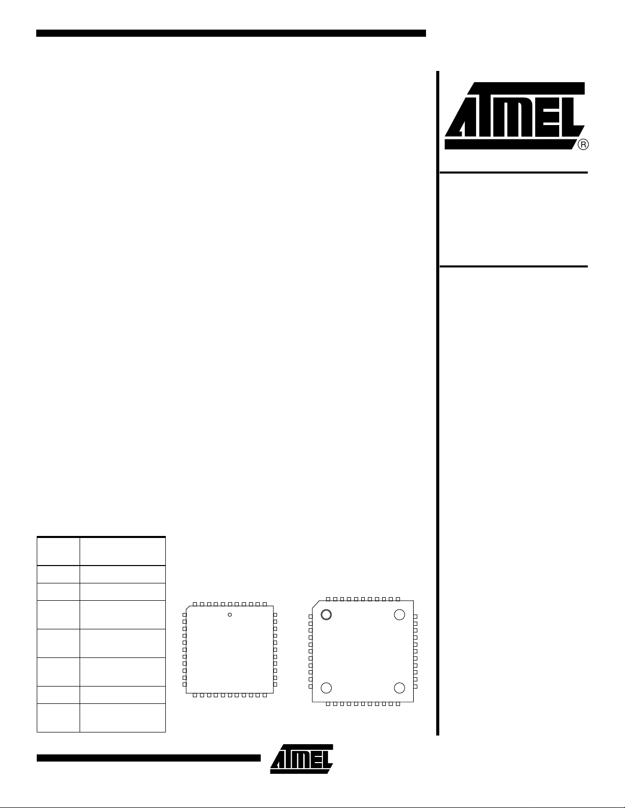
• Available in 44-pin PLCC and TQFP Packages
• Advanced Flash Technology
– 100% Tested
– Completely Reprogrammable
– 100 Program/Erase Cycles
– 20 Year Data Retention
– 2000V ESD Protection
– 200 mA Latch-up Immunity
• Supported By Popular 3rd Party Tools
• Security Fuse Feature
• Pin-compatible with the Most Commonly Used Devices
Highperformance
EPLD
ATF1500A
ATF1500AL
Description
The ATF1500A is a hig h-performance, hi gh-density complex PLD. Built on an
advanced Flash technol ogy, it has maxi mum pin to pin delay s of 7.5 ns and supports
sequential logic operati on at spee ds u p to 1 25 MHz . With 32 logic macro cell s and u p
to 36 inputs, it easily integrates logic from several TTL, SS I, MSI and classic PLDs.
The ATF1500A’s global input and feedback architecture simplifies logic placement
and eliminates pinout changes due to design changes.
Pin Configurations
Pin
Name Function
CLK Clock
I Logic Inputs
I/O
GCLR
OE1,
OE2
VCC +5V Supply
PD
Bidirectional
Buffers
Register Reset
(active low)
Output Enable
(active low)
Power Down
(active high)
PLCC
Top View
GND
VCC
I/O
I/O
4443424140393837363534
1
I/O
2
I/O
3
I/O
4
5
I/O
6
I/O
7
I/O
8
I/O
9
10
I/O
11
I/O
1213141516171819202122
I/O
I/O
(continued)
TQFP
Top View
I/O/PD
VCC
OE2/I
GCLR/I
OE1/I
I/O
I/O
I/O
VCC
GND
CLK/I
I/O
GND
I/O
I/O
I/O
33
I/O
32
I/O
31
I/O
30
I/O
29
VCC
28
I/O
27
I/O
26
I/O
25
I/O
24
GND
23
I/O
I/O
I/O
Rev. 0759E–06/99
1
Page 2
Functional Logic Diagram
(1)
Note: 1. Arrows connecting macrocells indicate direction and groupings of CASIN/CASOUT data flow.
The ATF1500A has 32 bi-directional I/O pins and 4 dedicated input pins. Eac h dedicate d input pin c an also serve
as a global control signal: register clock, register reset or
output enable. Each of these control signals can be
selected for use individually within each macrocell.
2
ATF1500A(L)
Each of the 32 logic macrocells generates a buried feedback, which goes to th e global bu s. Each inp ut and I/O pin
also feeds into the global bus. Because of this global bussing, each of these signals is always available to all 32
macrocells in the device.
Page 3
ATF1500A(L)
Each macrocell also generates a foldback logic term, which
goes to a regional bu s. Al l s ign al s wi thin a reg ion al bus are
connected to all 16 macrocells within the region.
Cascade logic between macrocells in the ATF1500A allows
fast, efficient generation of complex logic functions. Th e
ATF1500A co ntains 4 s uch lo gic ch ains, each capabl e of
creating sum term logic with a fa n in of up to 40 product
terms.
Bus Friendly Pin-Keeper Input and I/O’s
All Input and I/O pins on the ATF1500A have programma-
ble “pin keeper” circuits. If activated, when any pin is driven
high or low and then subsequently left floating, it will stay at
that previous high or low level.
This circuitry prevents unus ed Input and I/O lines from
floating to intermedi ate volta ge levels , which caus e unnecessary power consumption and system noise. The keeper
circuits eliminate the need for external pull-up resistors and
eliminate their DC power consumption.
Pin-keeper cir cuits can be disab led. Progr amming i s controlled in the logic design file. Once the pin-keeper circuits
are disabled, normal termination pr ocedures are r equired
for unused inputs and I/Os.
Speed/Power Management
The ATF1500A has seve ral built-i n spe ed and power m anagement features. The ATF1500A co ntains circuitry that
automatically puts the device into a low power stand-by
mode when no logic transitions are oc cu rrin g. Thi s not only
reduces power consumptio n during inactiv e periods, but
also provides a proportional power savings for most applications running at system speeds below 10 MHz.
All ATF1500As also have an optional pin-controlled power
down mode. In this mode, current drops to below 10 mA.
When the power down option is selected, the PD pin is
used to power down the part. The power down o ption is
selected in the desi gn source file. Whe n enabled, the
device goes into power down when the PD pin is high. In
the power down mode, all inter nal logi c si gnals ar e latche d
and held, as ar e any en abl ed out put s. Al l pin t rans itio ns ar e
ignored until the PD is brought low. When the power down
feature is enabled, the PD cannot be used as a logic input
or output. However, the PD pin's macrocell may still be
used to generate buried foldback and cascade logic s ignals.
Each output also has in divi dual sl ew rate contr ol. This may
be used to reduce system noise by slowing down o utputs
that do not need to operate at maximum speed. Outputs
default to slow switching, and may be specified as fas t
switching in the design file.
Design Software Support
ATF1500A designs are supported by several 3rd party
tools. Automated fitters allow logic synthesis using a variety
of high level description languages and formats.
Input Diagram
V
CC
INPUT
ESD
PROTECTION
CIRCUIT
100K
PROGRAMMABLE
OPTION
I/O Diagram
V
CC
OE
DATA
V
CC
100K
PROGRAMMABLE
OPTION
I/O
3
Page 4
ATF1500A(L) Macrocell
ATF1500A Macrocell
The ATF1500A macr ocell is flexible enou gh to support
highly complex logic functions operating at high speed. The
macrocell consists of five sections: product terms and product term select multiplexer; OR/XOR/CASCADE logic; a flip
flop; output select and enable; and logic array inputs.
Product Terms and Select Mux
Each ATF1500A macrocell has five pr oduct terms. Each
product term recei ve s a s its inp u ts al l s ig nal s f ro m bo th th e
global bus and regional bus.
The product term select multip lexer ( PTMUX ) alloc ates th e
five product terms as needed to the macrocell logic gates
and control signals. The PTMUX programming is determined by the design c ompiler, which se lects the opt imum
macrocell configuration.
OR/XOR/CASCADE Logic
The ATF1500A macrocell’s OR/XOR/CASCADE logic
structure is design ed to effi c ien tly su pport al l ty pes of log ic .
Within a single mac rocell, all the product term s can be
4
ATF1500A(L)
routed to the OR g ate, cr eating a fi ve input AND/OR sum
term. With the addition of the CASIN from neighboring
macrocells, this can be expanded to as many as 40 product
terms with a very small addition al del ay.
The macrocell’s XOR gate allows efficient implementation
of compare and arithmetic fun ctions. O ne input to the XOR
comes from the OR sum term. The other XOR input can be
a product term or a fixed high or low level. For combinatorial outputs, the fixed level input allows output polarity
selection. F or re gist ere d func tio ns, th e fix ed leve ls al low De
Morgan minimization of the product terms. The XOR gate is
also used to emulate T-type flip flops.
Flip Flop
The ATF1500A’s flip flop has very fle xible dat a and contro l
functions. The data input can come from either the XOR
gate or from a separate product term. Selecting the separate product term allows creation of a buried registered
feedback within a combinatorial output macrocell.
Page 5

ATF1500A(L)
In addition to D, T, JK and SR operation, the flip flop can
also be configured as a flow-through latch. In this mode,
data passes through when the clock is high and is latched
when the clock is low.
The clock itself can be e ither the global CLK pi n or an ind ividual product term. The flip flop changes state on the
clock’s rising edge. When the CLK pin is used as the clock,
one of the macrocell product terms can be selected as a
clock enable. When the cloc k enable func tion is active an d
the enable signal (produc t term) is low , all clo ck edges are
ignored.
The flip flop’s asynchronous reset signal (AR) can be either
the pin global clear (GCLR), a product term, or always off.
AR can also be a logic OR of GCLR with a product term.
The asynchronous preset (AP) can be a product term or
always off.
Output Select and Enable
The ATF1500A macro cell ou tput can be s elect ed as regi stered or combinatorial. When the outpu t is registered, the
same registered signal is fed back inte rnally to the g lobal
bus. When the output is combi nato rial , the buri ed fee dba ck
can be either the same combinatorial signal or it can be the
register output if the separate product term is chosen as
the flip flop input.
The output enable multiplexer (MOE) controls the output
enable signals . Any buffer ca n be perman ently enab led for
simple output operation. Buffers ca n also be permanently
disabled to allow use of the pin as an i nput. In this confi guration all the ma croce ll res our ces are still ava ilab le, i ncl uding the buried feedback, expander and CASCADE logic.
The output enable for each m acroce ll ca n als o be se lecte d
as either of the two OE pins or as an individual product
term.
Global/Regional Busses
The global bus contains all Input and I/O pin signals as well
as the buried feed back signal from a ll 32 macrocells.
Together with the complement of each signal, this provides
a 68 bit bus as input to every product term. Having the
entire global bus available to each macrocell eliminates
any potential routing proble ms. With this arc hitecture
designs can be modified without requiring pinout changes.
Each macrocell a lso generate s a foldbac k product ter m.
This signal goes to the regi onal bu s, and is av ailab le to 16
macrocells. The foldback is an inverse polarity of one of the
macrocell’s product terms. The 16 foldba ck terms in each
region allow generation of high fan-in sum terms (up to 21
product terms) with a small additional delay.
5
Page 6
Absolute Maximum Ratings*
Temperature Under Bias.................................. -40°C to +85°C
Storage Temperature..................................... -65°C to +150°C
Voltage on Any Pin with
Respect to Ground .........................................-2.0V to +7.0V
Voltage on Input Pins
with Respect to Ground
During Programming.....................................-2.0V to +14.0V
Programming Voltage with
Respect to Ground .......................................-2.0V to +14.0V
(1)
(1)
(1)
*NOTICE: Stresses beyond those listed under “Absolute
Maximum Ratings” may cause permanent da mage to the device . This is a st ress rating only and
functional operatio n of the dev ice at th ese or an y
other conditions beyond those indicated in the
operational sections of this specification is not
implied. Exposure to absolute maximum rating
conditions for exten ded periods may af fect device
reliability .
Note: 1. Minimum voltage is -0.6V DC, which may under-
shoot to -2.0V for pulses of less than 20 ns. Maximum output pin voltage is V
+ 0.75V DC,
CC
which may overshoot to 5.25V for pulses of less
than 20 ns.
DC and AC Operating Conditions
Commercial Industrial
Operating Temperature (ambient) 0°C - 70°C-40°C - 85°C
V
Power Supply 5V ± 5% 5V ± 10%
CC
DC Characteristics
Symbol Parameter Condition Min Typ Max Units
I
IL
I
IH
Input or I/O
Low Leakage Current
Input or I/O
High Leakage Current
≤ VIL (Max) -10 µA
0 ≤ V
IN
V
, Min ≤ VIN ≤ V
IH
CC
10 µA
Com. 70 mA
ATF1500A
I
CC1
(1)
Power Supply Current,
Standby
VCC = Max,
V
= 0, V
IN
CC
Ind. 100 mA
Com. 3 mA
ATF1500AL
Ind. 5 mA
I
I
V
V
V
V
CC2
OS
IL
IH
OL
OH
Power Supply Current,
Pin-Controlled Power
Down Mode
Output Short Circuit
Current
Input Low Voltage
Input High Voltage 2.0 VCC + 1 V
Output Low Voltage VCC = Min IOL = 12 mA 0.45 V
Output High Voltage VCC = Min
V
= Max,
CC
V
= 0, V
IN
V
OUT
VCC, Min < VCC
< VCC, Max
CC
= 0.5V -130 mA
-0.5 0.8 V
I
= -4 mA 2.4 V
OH
I
= -0.2 mA VCC - 0.2 V
OH
210mA
Note: 1. All ICC parameters measured with outputs open, and a 16-bit loadable, up/down counter programmed into each region.
6
ATF1500A(L)
Page 7

AC Waveforms
Register AC Characteristics, Input Pin Clock
-7 -10 -12 -15 -20 -25
Symbol Parameter
(1)
t
t
t
t
COS
CFS
SIS
SFS
Clock to Output 4.52526282929ns
Clock to Feedback 2 2 2 2 2 2 ns
I, I/O Setup Time 6 8 10 11 14 16 ns
Feedback Setup
Time
6 8 10 11 12 13 ns
ATF1500A(L)
UnitsMin Max Min Max Min Max Min Max Min Max Min Max
t
HS
t
PS
t
WS
Input, I/O, Feedback
Hold Time
Clock Period 6 8 9 10 11 12 ns
Clock Width3 44.555.56 ns
0 00000ns
External Feedback
+ t
+ t
COS
CFS
)
)
) 166.7 125 111 100 91 83 MHz
PS
2 33455ns
6 9 10 12 13 14 ns
F
MAXS
t
RPRS
t
RTRS
1/(t
SIS
Internal Feedback
1/(t
SFS
No Feedback 1/(t
Reset Pin Recovery
Time
Reset Term
Recovery Time
Note: 1. For slow slew outputs, add t
95 76.9 62.5 52.6 43 40 MHz
125 100 83.3 76.9 71 66 MHz
.
SSO
7
Page 8

Register AC Characteristics, Product Term Clock
-7 -10 -12 -15 -20 -25
Symbol Parameter
(1)
t
t
t
t
t
COA
CFA
SIA
SFA
HA
Clock to Output 7.5 10 12 15 18 20 ns
Clock to Feedback 5 7 7 9 12 15 ns
I, I/O Setup Time 3 3 4 4 8 10 ns
Feedback Setup
Time
Input, I/O, Feedback
Hold Time
3 3 4 4 12 15 ns
2 34455ns
UnitsMin Max Min Max Min Max Min Max Min Max Min Max
t
PA
t
WA
Clock Period 6 8 10 12 24 30 ns
Clock Width 3 4 5 6 12 15 ns
External Feedback
+ t
+ t
COA
CFA
)
)
) 166.7 125 100 83.3 41.7 33.3 MHz
PA
0000 00ns
4566 78ns
F
MAXA
t
RPRA
t
RTRA
1/(t
SIA
Internal Feedback
1/(t
SFA
No Feedback 1/(t
Reset Pin Recovery
Time
Reset Term
Recovery Time
Note: 1. For slow slew outputs, add t
95.2 76.9 62.5 52.6 38 33.3 MHz
125 100 90.9 76.9 41.7 33.3 MHz
.
SSO
8
ATF1500A(L)
Page 9

AC Characteristics
Symbol Parameter
ATF1500A(L)
-7 -10 -12 -15 -20 -25
UnitsMin Max Min Max Min Max Min Max Min Max Min Max
t
t
t
t
t
t
t
t
t
t
t
PD
PD2
PD3
PD4
EA
ER
PZX
PXZ
PF
PO
RPF
(1)
I, I/O or FB to
Non-Registered
27.5310312315320325 ns
Output
I, I/O to Feedback 5 7 8 9 12 14 ns
Feedback to
(1)
Non-Registered
27.5310312315320325 ns
Output
Feedback to
Feedback
(1)
OE Term to Output
Enable
OE Term to Output
Disable
OE Pin to Output
(1)
Enable
OE Pin to Output
Disable
1.5 5.5 1..5 7 1.5 8 1.5 9 1.5 10 1.5 11 ns
5 7 8 9 12 14 ns
27.5310312315320325 ns
27.5210212215220225 ns
25.52 7 2 8 2 9210211 ns
Preset to Feedback 6 9 9 12 18 20 ns
(1)
Preset to Registered
Output
Reset Pin to
Feedback
8.51214202325ns
34355.56ns
Reset Pin to
(1)
t
t
t
t
t
t
RPO
RTF
RTO
CAS
SSO
FLD
Registered Output
Reset Term to
Feedback
Reset Term to
(1)
Registered Output
Cascade Logic Delay 0.8 0.8 1 1 1.5 1.5 ns
Slow Slew Output
Adder
Foldback Term Delay 4 5 7 8 10 12 ns
Note: 1. For slow slew outputs, add t
5.5 7 8 11 13 15 ns
6 9 9 121520ns
8.51214202325ns
333444ns
.
SSO
9
Page 10

Power Down AC Characteristics
-7 -10 -12 -15 -20 -25
Symbol Parameter
UnitsMinMaxMinMaxMinMaxMinMaxMinMaxMinMax
t
IVDH
t
GVDH
t
CVDH
t
DHIX
t
DHGX
t
DHCX
t
DLIV
t
DLGV
t
DLCV
t
DLOV
(1)
Valid I, I/O Before
PD High
Valid OE
(2)
Before PD High
Valid Clock
(2)
Before PD High
Input Don’t Care
After PD High
OE Don’t Care
After PD High
Clock Don’t Care
After PD High
PD Low to Valid I,
I/O
PD Low to Valid
(2)
OE
PD Low to Valid
(2)
Clock
PD Low to Valid
Output
Notes: 1. For slow slew outputs, add t
2. Pin or Product Term.
7 1012152025 ns
7 1012152025 ns
7 1012152025 ns
15 20 22 25 30 35 ns
15 20 22 25 30 35 ns
15 20 22 25 30 35 ns
111111µs
111111µs
111111µs
111111µs
.
SSO
Input Test Waveforms and
Output Test Load
Measurement Levels
AC
DRIVING
LEVELS
3.0V
0.0V
1.5V
t
, tf 1.5 ns
r
AC
MEASUREMENT
LEVEL
Pin Capacitance
f = 1 MHz, T = 25°C
C
IN
C
OUT
Note: 1. Typical values for nominal supply voltage. This parameter is only sampled and is not 100% tested.
10
(1)
Typ Max Units Conditions
4.5 5.5 pF VIN = 0V
3.5 4.5 pF V
ATF1500A(L)
OUT
= 0V
Page 11

ATF1500A(L)
Power Up Reset
The ATF1500A’s registers are designed to reset during
power up. At a point delayed slightly from V
, all registers will be re set to th e low st ate. As a r esult,
V
RST
crossing
CC
the registered output state will always be low on power-up.
This feature is critical for state machine initialization. How-
ever, due to the asynchronous nature of reset and the
uncertainty of h ow V
actually rises in the sys tem, the fo l-
CC
lowing conditions are required:
1. The V
rise must be monotonic, from below 0.7 volt,
CC
2. After reset occurs, all input and feedback setup times
must be met before driving the clock signal high, and
3. Signals from which clocks are derived must remain stable during t
PR
.
Power Down Mode
The ATF1500A includes an optional pin controlled power
down feature. When this mod e is enab led, the P D pin acts
as the power down pin. When the PD pin is high, the device
supply current is reduced to less than 10 mA. During power
down, all output data and internal logic states are latched
and held. Therefore, all registered and combinatorial output
data remain valid. Any outputs which were in a HI-Z state at
the onset of power down will r emain at HI-Z. During power
down, all input signals except the power down pin are
blocked. Input an d I/O hol d latche s rema in activ e to insur e
that pins do not fl oat to inde termina te leve ls, f urther reducing system power. The power down pin feature is enabled
in the logic design file. Designs using the power down pin
may not use the PD pin logic array input. However, all other
PD pin macrocell resources may still be used, including the
buried feedback and foldback product term array inputs.
preload mode i s enab led by r aising an inp ut pin to a h igh
voltage level. Contact Atmel PLD Applications for PRELOAD pin assignments, timing and voltage requirements.
Parameter Description Typ Max Units
t
PR
V
RST
Power-Up
Reset Time
Power-Up
Reset
Voltage
210 µs
3.8 4.5 V
Output Slew Rate Control
Each ATF1500A macrocell contains a configuration bit for
each I/O to control its output slew rate. This allows selected
data paths to operate at ma ximu m th roughput while redu cing system noise from outputs that are not speed-critical.
Outputs default to slow edges, and may be individually set
to fast in the design file. O utput transitio n times for outp uts
configured as “slow” have a t
delay adder.
SSO
Register Preload
The ATF1500A’s registers are provided with circuitry to
allow loading of each register with either a high or a low.
This feature will simplify testing since an y state can be
forced into the registers to control test sequencing. A
JEDEC file with preload is generated whe n a source fil e
with preload vectors is compiled. Once downloaded, the
JEDEC file preload sequence will be done automatica lly
when vectors are run by any approved programmers. The
Security Fuse Usage
A single fuse is provided to prevent unauthoriz ed copying
of the ATF1500A fuse patterns. Once programmed, fuse
verify and preload are prohibited. However, the 160-bit
User Signature remains accessible.
The security fuse should be programmed last, as its effect
is immediate.
11
Page 12

NORMALIZED SUPPLY CURRENT
vs. INPUT FREQUENCY
(V
ATF1500A
I
CC
= 5V, TA = 25˚C)
cc
I
mA
CC
SUPPLY CURRENT
vs. FREQUENCY
ATF1500AL (V
= 5V, TA = 25˚C)
CC
NORMALIZED SUPPLY CURRENT
vs. SUPPLY VOLTAGE
ATF1500 (TA = 25˚C)
I
CC
OUTPUT SOURCE CURRENT
vs. SUPPLY VOLTAGE (V
I
OH
= 2.4V, TA = 25˚C)
OH
ICC mA
I
mA
OL
NORMALIZED SUPPLY CURRENT
vs. AMBIENT TEMPERATURE
ATF1500 (V
CC
= 5V)
OUTPUT SINK SURRENT
vs. SUPPLY VOLTAGE (TA = 25˚C, V
= 0.45V)
OL
12
vs. OUTPUT VOLTAGE (V
IOH mA
ATF1500A(L)
OUTPUT SOURCE CURRENT
= 2.4V, TA = 25˚C)
OH
I
OH
vs. OUTPUT VOLTAGE (V
OUTPUT SOURCE CURRENT
mA
= 5V, TA = 25˚C)
CC
Page 13

ATF1500A(L)
INPUT CURRENT vs. INPUT VOLTAGE
(V
CC
= 5V, TA = 25˚C)
vs. OUTPUT VOLTAGE (V
OUTPUT SINK CURRENT
I
mA
OL
= 5V, TA = 25˚C)
CC
INPUT CLAMP CURRENT
vs. INPUT VOLTAGE
t
t
COS
PD
NORMALIZED t
vs. AMBIENT TEMPERATURE (V
NORMALIZED t
vs. AMBIENT TEMPERATURE (VCC = 5V)
PD
COS
= 5V)
CC
NORMALIZED t
vs. SUPPLY VOLTAGE (TA = 25˚C)
t
COS
COS
t
COA
NORMALIZED t
vs. AMBIENT TEMPERATURE (VCC = 5V)
COA
13
Page 14

t
SIS
vs. SUPPLY VOLTAGE (TA = 25˚C)
NORMALIZED t
SIS
t
SIS
NORMALIZED t
vs. AMBIENT TEMPERATURE (VCC = 5V)
SIS
t
SIA
NORMALIZED t
vs. SUPPLY VOLTAGE (TA = 25˚C)
SIA
t
SIA
NORMALIZED t
vs. AMBIENT TEMPERATURE (VCC = 5V)
SIA
14
ATF1500A(L)
Page 15

Ordering Information
ATF1500A(L)
t
PD
(ns)
7.5 4.5 95 ATF1500A-7AC
10 5 76.9 ATF1500A-10AC
12 6 62.5 ATF1500A-12AC
15 8 52.6 ATF1500A-15AC
20 9 40 ATF1500AL-20AC
t
COS
(ns)
F
MAX
(MHz) Ordering Code Package Operation Range
ATF1500A-7JC
ATF1500A-10JC
ATF1500A-10AI
ATF1500A-10JI
ATF1500A-12JC
ATF1500A-12AI
ATF1500A-12JI
ATF1500A-15JC
ATF1500A-15AI
ATF1500A-15JI
ATF1500AL-20JC
ATF1500AL-20AI
ATF1500AL-20JI
44A
44J
44A
44J
44A
44J
44A
44J
44A
44J
44A
44J
44A
44J
44A
44J
44A
44J
Commercial
(0°C to 70°C)
Commercial
(0°C to 70°C)
Industrial
(-40°C to 85°C)
Commercial
(0°C to 70°C)
Industrial
(-40°C to 85°C)
Commercial
(0°C to 70°C)
Industrial
(-40°C to 85°C)
Commercial
(0°C to 70°C)
Industrial
(-40°C to 85°C)
25 9 43 ATF1500AL-25AC
ATF1500AL-25JC
ATF1500AL-25AI
ATF1500AL-25JI
44A
44J
44A
44J
Commercial
(0°C to 70°C)
Industrial
(-40°C to 85°C)
Using “C” Product for Industrial
To use commercial product for Industrial temperature ranges, down-grade one speed grade from the “I” to the “C” device
(7 ns “C” = 10 ns “I”) and de-rate power by 30%.
Package Type
44A 44-lead, Thin Plastic Gull Wing Quad Flatpack (TQFP)
44J 44-lead, Plastic J-leaded Chip Carrier (PLCC)
15
Page 16

Packaging Information
44A, 44-lead, Thin (1.0 mm)
Plastic Gull Wing Quad Flat Package (TQFP)
Dimensions in Millimeters and (Inches)*
12.21(0.478)
11.75(0.458)
10.10(0.394)
9.90(0.386)
0.15(0.006)
0.05(0.002)
0.80(0.031) BSC
0.20(.008)
0.09(.003)
PIN 1 ID
0
7
0.75(0.030)
0.45(0.018)
SQ
0.45(0.018)
0.30(0.012)
SQ
1.20(0.047) MAX
44J, 44-lead, Plastic J-leaded Chip Carrier (PLCC)
Dimensions in Inches and (Millimeters)
.045(1.14) X 45°
.032(.813)
.026(.660)
.050(1.27) TYP
PIN NO.1
IDENTIFY
.045(1.14) X 30° - 45°
.656(16.7)
SQ
.650(16.5)
.695(17.7)
.685(17.4)
.500(12.7) REF SQ
.022(.559) X 45° MAX (3X)
SQ
.012(.305)
.008(.203)
.630(16.0)
.590(15.0)
.021(.533)
.013(.330)
.043(1.09)
.020(.508)
.120(3.05)
.090(2.29)
.180(4.57)
.165(4.19)
*Controlling dimension: millimeters
16
ATF1500A(L)
Page 17

Atmel Headquarters Atmel Operations
Corporate Headquarters
2325 Orchard Parkway
San Jose, CA 95131
TEL (408) 441- 0311
FAX (408) 487-2600
Europe
Atmel U.K., Ltd.
Coliseum Business Centre
Riverside Way
Camberley, Surrey GU15 3YL
England
TEL (44) 1276-686-677
FAX (44) 1276-686-697
Asia
Atmel Asia, Ltd.
Room 1219
Chinachem Golden Plaza
77 Mody Road Tsimhatsui
East Kowloon
Hong Kong
TEL (852) 2721 -9778
FAX (852) 2722-1369
Japan
Atmel Japan K.K.
9F, Tonetsu Shinkawa Bldg.
1-24-8 Shink awa
Chuo-ku, Tokyo 104-0033
Japan
TEL (81) 3-3523-3551
FAX (81) 3-3523-7581
Atmel Colorado Springs
1150 E. Cheyenne Mtn. Blvd.
Colorado Springs, CO 80906
TEL (719) 576-3300
FAX (719) 540-1759
Atmel Rousset
Zone Indu strie lle
13106 Rousset Cedex
France
TEL (33) 4-4253-6000
FAX (33) 4-4253-6001
Fax-on-Demand
North America:
1-(800) 292-8635
International:
1-(408) 441-0732
e-mail
literature@atmel.com
Web Site
http://www.atmel.com
BBS
1-(408) 436-4309
© Atmel Corporation 1999.
Atmel Corporation makes no warranty for the use of its products, other than those expressly contained in the Company’s standard warranty which is detailed in Atmel’s Terms and Conditions located on the Company’s web site. The Company assumes no responsibility for
any errors which may appear in this document, reserves the right to change devices or specifications detailed herein at any time without
notice, and does not make any commitment to update the information contained herein. No licenses to patents or other intellectual property of Atmel are granted by the Company in connection with the sale of Atmel products, expressly or by implication. Atmel’s products are
not authorized for use as critical components in life support devices or systems.
Marks bearing ® and/or ™ are registered trademarks and trademarks of Atmel Corporation.
Terms and product names in this document may be trademarks of others.
Printed on recycled paper.
0759E–06/99/xM
 Loading...