

Page 1
Features
• Operates between 2.7V to 5.5V
• High-density, High-performance Electrically-erasable Complex
Programmable Logic Device
– 44-pin, 32 I/O CPLD
– 100% connected
– 12 ns Maximum Pin-to-pin Delay
– Registered Operation up to 90.9 MHz
– Fully Connected Input and Feedback Logic Array
• Flexible Logic Macrocell
– D/T/Latch Configurable Flip-flops
– Global and Individual Register Control Signals
– Global and Individual Output Enable
– Programmable Output Slew Rate
• Advanced Power Management Features
– Pin-controlled 5 µA Standby Mode (Typical)
– Programmable Pin-keeper Inputs and I/Os
• Available in Commercial and Industrial Temperature Ranges
• Available in 44-lead PLCC and TQFP Packages
• Advanced EEPROM Technology
– 100% Tested
– Completely Reprogrammable
– 10,000 Program/Erase Cycles
– 20-year Data Retention
– 2000V ESD Protection
– 200 mA Latchup Immunity
• Supported by Popular Third-party Tools
• Security Fuse Feature
Highperformance
EE PLD
ATF1500ABV
Description
The ATF1500ABV is a high-performance, high-density complex PLD. Built on an
advanced EEPROM technology, it has maximum pin-to-pin delays of 12 ns and supports sequential logic operation at speeds up to 90.9 MHz. With 32 logic macrocells
and up to 36 inputs, it easily integrates logic from several TTL, SSI, MSI and classic
PLDs.
Pin Configurations
Pin
Name Function
CLK Clock
I Logic Inputs
I/O Bi-directional
Buffers
GCLR Register Reset
(active low)
OE1,
OE2
Output Enable
(active low)
VCC (+3V to 5.25V)
Supply
PD Power-down
(active high)
I/O
I/O
65432
7
I/O
8
I/O
9
I/O
10
GND
11
I/O
12
I/O
13
I/O
14
I/O
15
VCC
16
I/O
17
I/O
1819202122232425262728
I/O
I/O
PLCC
Top View
I/O/PD
VCC
OE2/I
GCLR/I
OE1/I
1
4443424140
I/O
I/O
I/O
VCC
GND
CLK/I
I/O
GND
I/O
I/O
I/O
39
I/O
I/O
I/O
I/O
I/O
VCC
I/O
I/O
I/O
I/O
GND
I/O
GND
VCC
1
I/O
2
I/O
3
4
I/O
5
I/O
6
I/O
7
I/O
8
9
I/O
10
I/O
11
38
37
36
35
34
33
32
31
30
29
I/O
I/O
TQFP
Top View
I/O
I/O
I/O/PD
VCC
OE2/I
GCLR/I
OE1/I
CLK/I
GND
I/O
4443424140393837363534
1213141516171819202122
I/O
I/O
I/O
I/O
I/O
I/O
I/O
I/O
VCC
GND
I/O
I/O
33
I/O
32
I/O
31
I/O
30
VCC
29
I/O
28
I/O
27
I/O
26
I/O
25
GND
24
I/O
23
I/O
Rev. 0723I–08/01
1
Page 2
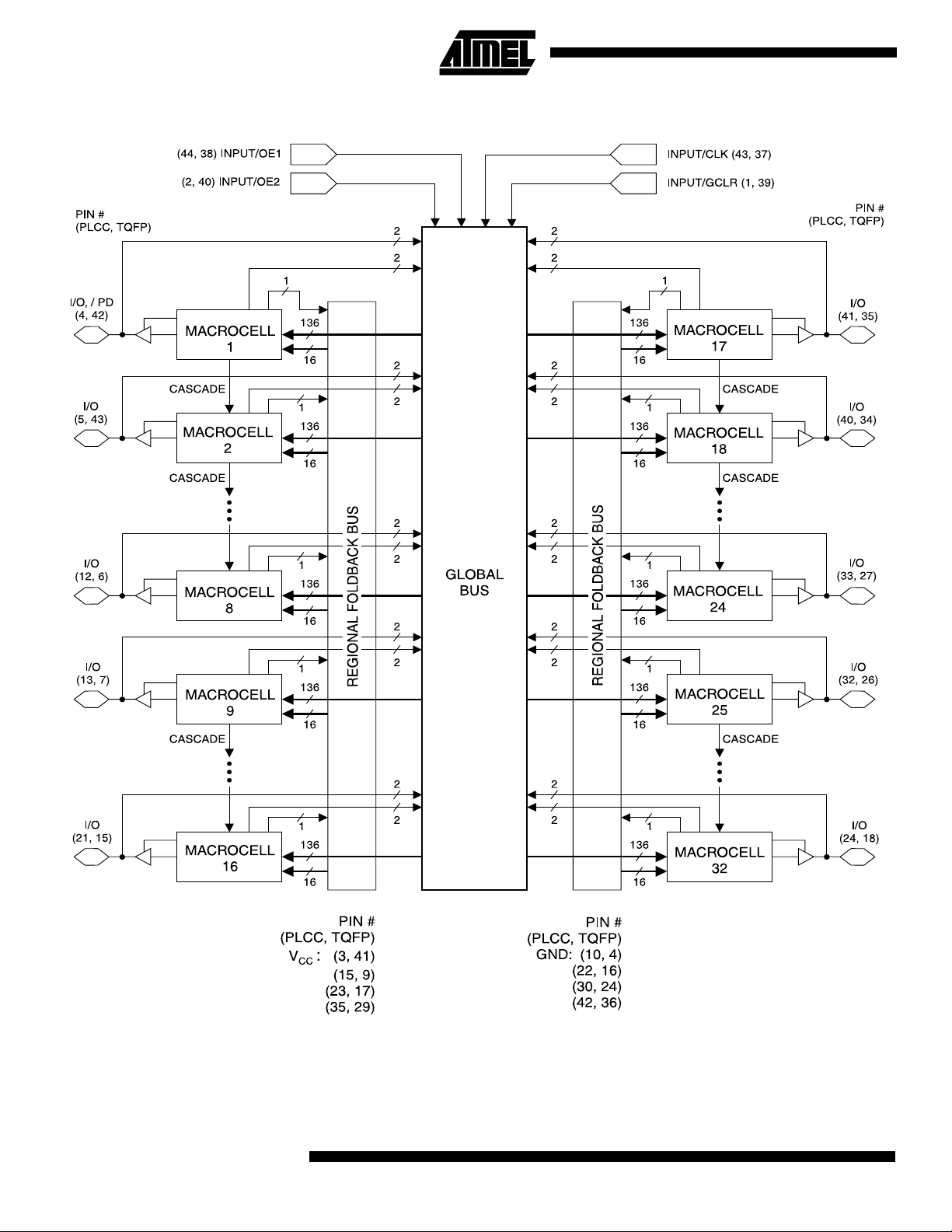
Functional Logic Diagram
(1)
Note: 1. Arrows connecting macrocells indicate direction and groupings of CASIN/CASOUT data flow.
2
ATF1500ABV
0723I–08/01
Page 3

ATF1500ABV
The ATF1500ABV’s 100% connected global input and feedback architecture simplifies logic
placement and eliminates pinout changes due to design changes. Any Macrocell may be connected to any I/O pin.
The ATF1500ABV has 32 bi-directional I/O pins and four dedicated input pins. Each dedicated
input pin can also serve as a global control signal: register clock, register reset or output
enable. Each of these control signals can be selected for use individually within each
macrocell.
Each of the 32 logic macrocells generates a buried feedback, which goes to the global bus.
Each input and I/O pin also feeds into the global bus. Because of this global busing, each of
these signals is always available to all 32 macrocells in the device.
Each macrocell also generates a foldback logic term, which goes to a regional bus. All signals
within a regional bus are connected to all 16 macrocells within the region.
Cascade logic between macrocells in the ATF1500ABV allows fast, efficient generation of
complex logic functions. The ATF1500ABV contains four such logic chains, each capable of
creating sum term logic with a fan-in of up to 40 product terms.
Bus-friendly Pin-keeper Input and I/Os
Speed/Power Management
All input and I/O pins on the ATF1500ABV have programmable “data-keeper” circuits. If acti-
vated, when any pin is driven high or low and then subsequently left floating, it will stay at that
previous high or low level.
This circuitry prevents unused input and I/O lines from floating to intermediate voltage levels
that cause unnecessary power consumption and system noise. The keeper circuits eliminate
the need for external pull-up resistors and eliminate their DC power consumption.
Pin-keeper circuits can be disabled. Programming is controlled in the logic design file. Once
the pin-keeper circuits are disabled, normal termination procedures are required for unused
inputs and I/Os.
The ATF1500ABV has several built-in speed and power management features. The
ATF1500ABV contains circuitry that automatically puts the device into a low-power standby
mode when no logic transitions are occurring. This not only reduces power consumption during inactive periods, but also provides proportional power savings for most applications
running at system speeds below 10 MHz.
All ATF1500ABVs also have an optional pin-controlled power-down mode. In this mode, current drops to typically 2 mA. When the power-down option is selected, the PD pin is used to
power-down the part. The power-down option is selected in the design source file. When
enabled, the device goes into power-down when the PD pin is high. In the power-down mode,
all internal logic signals are latched and held, as are any enabled outputs. All pin transitions
are ignored until the PD is brought low. When the power-down feature is enabled, the PD cannot be used as a logic input or output. However, the PD pin’s macrocell may still be used to
generate buried foldback and cascade logic signals.
0723I–08/01
Each output also has individual slew rate control. This may be used to reduce system noise by
slowing down outputs that do not need to operate at maximum speed. Outputs default to slow
switching, and may be specified as fast switching in the design file.
3
Page 4
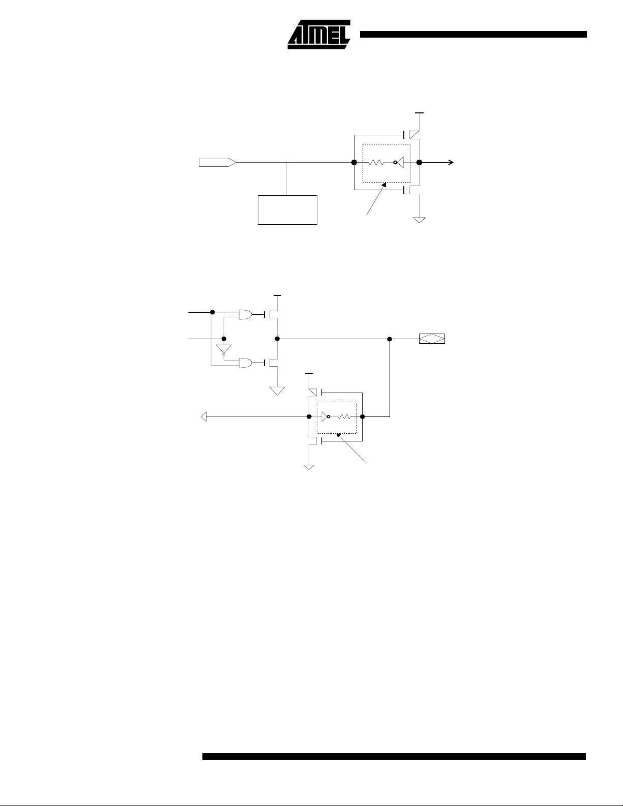
Input Diagram
I/O Diagram
INPUT
OE
ESD
PROTECTION
CIRCUIT
V
CC
100K
PROGRAMMABLE
OPTION
V
CC
Design Software Support
DATA
V
CC
100K
PROGRAMMABLE
OPTION
I/O
ATF1500ABV designs are supported by several third-party tools. Automated fitters allow logic
synthesis using a variety of high level description languages and formats.
4
ATF1500ABV
0723I–08/01
Page 5
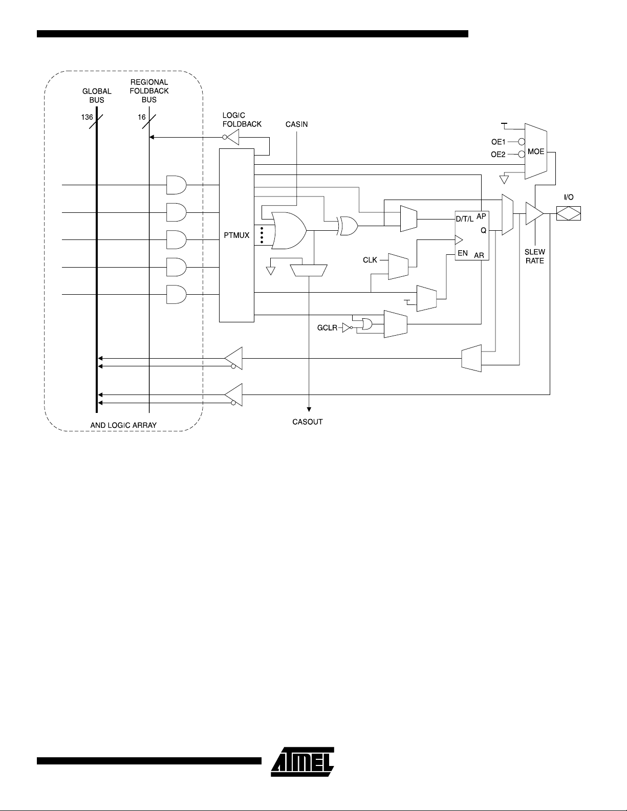
ATF1500ABV Macrocell
ATF1500ABV
ATF1500ABV Macrocell
Product Terms and Select Mux
OR/XOR/ CASCADE Logic
The ATF1500ABV macrocell is flexible enough to support highly complex logic functions operating at high speed. The macrocell consists of five sections: product terms and product term
select multiplexer; OR/XOR/CASCADE logic; a flip-flop; output select and enable; and logic
array inputs.
Each ATF1500ABV macrocell has five product terms. Each product term receives as its inputs
all signals from both the global bus and regional bus.
The product term select multiplexer (PTMUX) allocates the five product terms as needed to
the macrocell logic gates and control signals. The PTMUX programming is determined by the
design compiler, which selects the optimum macrocell configuration.
The ATF1500ABV macrocell’s OR/XOR/CASCADE logic structure is designed to efficiently
support all types of logic. Within a single macrocell, all the product terms can be routed to the
OR gate, creating a five-input AND/OR sum term. With the addition of the CASIN from neighboring macrocells, this can be expanded to as many as 40 product terms with little small
additional delay.
The macrocell’s XOR gate allows efficient implementation of compare and arithmetic functions. One input to the XOR comes from the OR sum term. The other XOR input can be a
product term or a fixed high or low level. For combinatorial outputs, the fixed-level input allows
output polarity selection. For registered functions, the fixed levels allow De Morgan minimization of the product terms. The XOR gate is also used to emulate JK-type flip-flops.
0723I–08/01
5
Page 6

Flip-flop The ATF1500ABV’s flip-flop has very flexible data and control functions. The data input can
come from either the XOR gate or from a separate product term. Selecting the separate product term allows creation of a buried registered feedback within a combinatorial output
macrocell.
In addition to D, T, JK and SR operation, the flip-flop can also be configured as a flow-through
latch. In this mode, data passes through when the clock is high and is latched when the clock
is low.
The clock itself can be either the global CLK pin or an individual product term. The flip-flop
changes state on the clock’s rising edge. When the CLK pin is used as the clock, one of the
macrocell product terms can be selected as a clock enable. When the clock enable function is
active and the enable signal (product term) is low, all clock edges are ignored.
The flip-flop’s asynchronous reset signal (AR) can be either the pin global clear (GCLR), a
product term, or always off. AR can also be a logic OR of GCLR with a product term. The
asynchronous preset (AP) can be a product term or always off.
Output Select and Enable
Global/Regional Buses
The ATF1500ABV macrocell output can be selected as registered or combinatorial. When the
output is registered, the same registered signal is fed back internally to the global bus. When
the output is combinatorial, the buried feedback can be either the same combinatorial signal or
it can be the register output if the separate product term is chosen as the flip-flop input.
The output enable multiplexer (MOE) controls the output enable signals. Any buffer can be
permanently enabled for simple output operation. Buffers can also be permanently disabled to
allow use of the pin as an input. In this configuration all the macrocell resources are still available, including the buried feedback, expander and CASCADE logic.
The output enable for each macrocell can also be selected as either of the two OE pins or as
an individual product term.
The global bus contains all input and I/O pin signals as well as the buried feedback signal from
all 32 macrocells. Together with the complement of each signal, this provides a 68-bit bus as
input to every product term. Having the entire global bus available to each macrocell eliminates any potential routing problems. With this architecture designs can be modified without
requiring pinout changes.
Each macrocell also generates a foldback product term. This signal goes to the regional bus,
and is available to 16 macrocells. The foldback is an inverse polarity of one of the macrocell’s
product terms. The 16 foldback terms in each region allow generation of high fan-in sum terms
(up to 21 product terms) with little additional delay.
6
ATF1500ABV
0723I–08/01
Page 7

ATF1500ABV
Absolute Maximum Ratings*
Temperature Under Bias................................ -55°C to +125°C
Storage Temperature..................................... -65°C to +150°C
Voltage on Any Pin with
Respect to Ground .......................................-2.0V to +5.25V
(1)
Voltage on Input Pins
with Respect to Ground
During Programming.....................................-2.0V to +14.0V
Programming Voltage with
Respect to Ground .......................................-2.0V to +14.0V
(1)
(1)
DC and AC Operating Conditions
Commercial Industrial
Operating Temperature (Ambient) 0°C - 70°C-40°C - 85°C
*NOTICE: Stresses beyond those listed under “Absolute
Maximum Ratings” may cause permanent damage to the device. This is a stress rating only and
functional operation of the device at these or any
other conditions beyond those indicated in the
operational sections of this specification is not
implied. Exposure to absolute maximum rating
conditions for extended periods may affect
device reliability.
Note: 1. Minimum voltage is -0.6V DC, which may under-
shoot to -2.0V for pulses of less than 20 ns.
Maximum out put pin voltage is V
which may overshoot to 5.25V for pulses of less
than 20 ns.
+ 0.75V DC,
CC
V
Power Supply 2.7V - 5.5V 2.7V - 5.5V
CC
DC Characteristics
Symbol Parameter Condition Min Typ Max Units
I
IL
I
IH
(1)
I
CC1
I
Power Supply Current,
CC2
I
OS
V
IL
V
IH
V
OL
V
OH
Note: 1. All ICC parameters measured with outputs open, and a 16-bit loadable, up/down counter programmed into each region.
Input or I/O
0 ≤ VIN ≤ VIL(max) -10 µA
Low Leakage Current
Input or I/O
VIH,min < VIN ≤ V
CC
10 µA
High Leakage Current
Power Supply Current,
Standby
VCC = MAX,
= 0, V
V
IN
CC
ATF1500ABV Com. 35 mA
Ind. 40 mA
ATF1500ABVL Com. 3 mA
Ind. 5 mA
Power Down Mode
Output Short Circuit
VCC = MAX,
V
= 0, V
IN
V
OUT
CC
= 0.5V -130 mA
2mA
Current
Input Low Voltage VCC, min < VCC
, max
< V
CC
-0.5 0.8 V
Input High Voltage 2.0 VCC + 1 V
Output Low Voltage VCC = MIN IOL = 4 mA 0.45 V
Output High Voltage VCC = MIN IOH = -0.1 mA VCC - .2 V
0723I–08/01
7
Page 8

AC Waveforms
Register AC Characteristics, Input Pin Clock
(1)
Symbol Parameter 2.7-volt Adder
(2)
t
COS
t
CFS
t
SIS
t
SFS
t
HS
t
PS
t
WS
f
MAXS
t
RPRS
t
RTRS
Clock to Output .5 2728 ns
Clock to Feedback 033ns
I, I/O Setup Time 11011ns
Feedback Setup Time 11011ns
Input, I/O, Feedback Hold Time 00 0 ns
Clock Period 113 14 ns
Clock Width .5 6.5 7 ns
External Feedback 1/(t
Internal Feedback 1/(t
No Feedback 1/(t
PS
+ t
SIS
SFS
) -5 58.8 52.6 MHz
COS
+ t
) -5.5 76.9 71.4 MHz
CFS
) -5.5 76.9 71.4 MHz
Reset Pin Recovery Time 13 4 ns
Reset Term Recovery Time 110 12 ns
Notes: 1. AC Characteristics are for VCC = 3.0 volts. For 2.7 volts, add the “2.7-volt adder.”
2. For slow slew outputs, add t
SSO
.
-12 -15
UnitsMin Max Min Max
= Preliminary Information
8
ATF1500ABV
0723I–08/01
Page 9

ATF1500ABV
Register AC Characteristics, Product Term Clock
(1)
Symbol Parameter 2.7-volt Adder
(2)
t
COA
t
CFA
t
SIA
t
SFA
t
HA
t
PA
t
WA
f
MAXA
Clock to Output 21215ns
Clock to Feedback 1 8 10 ns
I, I/O Setup Time 04 4 ns
Feedback Setup Time 04 4 ns
Input, I/O, Feedback Hold Time 04 4 ns
Clock Period 112 14 ns
Clock Width .5 6 7 ns
External Feedback 1/(t
Internal Feedback 1/(t
SIA
SFA
+ t
) -7 62.5 52.6 MHz
COA
+ t
) -6.4 83.3 71.4 MHz
CFA
No Feedback 1/(tPA) -6.4 83.3 71.4 MHz
t
RPRA
t
RTRA
Reset Pin Recovery Time 00 0 ns
Reset/Preset Term Recovery Time 06 6 ns
Notes: 1. AC Characteristics are for VCC = 3.0 volts. For 2.7 volts, add the “2.7-volt Adder.”
2. For slow slew outputs, add t
AC Characteristics
(1)
SSO
.
-12 -15
UnitsMin Max Min Max
Symbol Parameter 2.7-volt Adder
(2)
t
t
t
t
t
t
t
t
t
t
t
t
t
t
t
t
t
PD
PD2
PD3
PD4
EA
ER
PZX
PXZ
PF
PO
RPF
RPO
RTF
RTO
CAS
SSO
FLD
(2)
(2)
(2)
(2)
(2)
(2)
I, I/O or FB to Non-Registered Output 2 312315 ns
I, I/O to Feedback 189ns
Feedback to Non-Registered Output 2 312315 ns
Feedback to Feedback 189ns
OE Term to Output Enable 1 312315 ns
OE Term to Output Disable 1 212215 ns
OE Pin to Output Enable 12829ns
OE Pin to Output Disable 1 1.5 8 1.5 9 ns
Preset To Feedback 1912ns
Preset to Registered Output 21420ns
Reset Pin to Feedback 135ns
Reset Pin to Registered Output 1811ns
Reset Term to Feedback 1912ns
Reset Term to Registered Output 21420ns
Cascade Logic Delay 011ns
Slow Slew Output Adder 034ns
Foldback Term Delay 178ns
Notes: 1. AC Characteristics are for VCC = 3.0 volts. For 2.7 volts, add the “2.7-volt Adder.”
2. For slow slew outputs, add t
SSO
.
-12 -15
UnitsMin Max Min Max
= Preliminary Information
0723I–08/01
9
Page 10

Power-down AC Characteristics
(1)
-12 -15
Symbol Parameter 2.7-volt Adder
t
IVDH
t
GVDH
t
CVDH
t
DHIX
t
DHGX
tDHCX Clock Don't Care after PD High
t
DLIV
t
DLGV
t
DLCV
(2)
t
DLOV
Valid I, I/O before PD High 112 15 ns
Valid OE
Valid Clock
(3)
before PD High 112 15 ns
(3)
before PD High 112 15 ns
Input Don't Care after PD High 122 25 ns
OE Don't Care after PD High 122 25 ns
122 25 ns
PD Low to Valid I, I/O 011µs
PD Low to Valid OE
PD Low to Valid Clock
(3)
(3)
011µs
011µs
PD Low to Valid Output 011µs
Notes: 1. AC Characteristics are for VCC = 3.0 volts. For 2.7 volts, add the “2.7-volt Adder.”
2. For slow slew outputs, add t
SSO
.
3. Pin or Product Term.
Input Test Waveforms and Measurement Levels
UnitsMinMaxMinMax
= Preliminary Information
Output Test Load
Pin Capacitance
(f = 1 MHz, T = 25°C)
C
IN
C
OUT
Note: 1. Typical values for nominal supply voltage. This parameter is only sampled and is not 100% tested.
10
ATF1500ABV
(1)
Typ Max Units Conditions
4.5 5.5 pF VIN = 0V
3.5 4.5 pF V
OUT
= 0V
0723I–08/01
Page 11

ATF1500ABV
Power-up Reset The ATF1500ABV’s registers are designed to reset during power-up. At a point delayed
slightly from V
crossing V
CC
istered output state will always be low on power-up.
This feature is critical for state machine initialization. However, due to the asynchronous
nature of reset and the uncertainty of how V
tions are required:
1. The V
rise must be monotonic, from below 0.7 volts.
CC
2. Signals from which clocks are derived must remain stable during T
3. After T
occurs, all input and feedback setup times must be met before driving the
PR
clock signal high.
, all registers will be reset to the low state. As a result, the reg-
RST
actually rises in the system, the following condi-
CC
.
PR
Power-down Mode
Register Preload
The ATF1500ABV includes an optional pin-controlled power-down feature. When this mode is
enabled, the PD pin acts as the power-down pin. When the PD pin is high, the device supply
current is reduced to less than 10 µA. During power-down, all output data and internal logic
states are latched and held. Therefore, all registered and combinatorial output data remain
valid. Any outputs that were in a High-Z state at the onset of power-down will remain at
High-Z. During power-down, all input signals except the power-down pin are blocked. Input
and I/O hold latches remain active to ensure that pins do not float to indeterminate levels, further reducing system power. The power-down pin feature is enabled in the logic design file.
Designs using the power-down pin may not use the PD pin logic array input. However, all
other PD pin macrocell resources may still be used, including the buried feedback and foldback product term array inputs.
The ATF1500ABV’s registers are provided with circuitry to allow loading of each register with
either a high or a low. This feature will simplify testing since any state can be forced into the
registers to control test sequencing. A JEDEC file with preload is generated when a source file
with preload vectors is compiled. Once downloaded, the JEDEC file preload sequence will be
done automatically when vectors are run by any approved programmers. The preload mode is
enabled by raising an input pin to a high voltage level. Contact Atmel PLD Applications for
PRELOAD pin assignments, timing and voltage requirements.
0723I–08/01
Parameter Description Typ Max Units
Power-up
T
PR
V
RST
Reset Time
Power-up
Reset
Voltage
210 µs
2.2 2.7 V
11
Page 12

Output Slew Rate Control
Each ATF1500ABV macrocell contains a configuration bit for each I/O to control its output
slew rate. This allows selected data paths to operate at maximum throughput while reducing
system noise from outputs that are not speed-critical. Outputs default to slow edges, and may
be individually set to fast in the design file. Output transition times for outputs configured as
“slow” have a t
delay adder.
SSO
Security Fuse Usage
A single fuse is provided to prevent unauthorized copying of the ATF1500ABV fuse patterns.
Once programmed, fuse verify and preload are prohibited. However, the 160-bit User Signature remains accessible.
The security fuse should be programmed last, as its effect is immediate.
12
ATF1500ABV
0723I–08/01
Page 13

Ordering Information
ATF1500ABV
t
PD
(ns)
12 6 62.5 ATF1500ABV-12AC
15 8 52.6 ATF1500ABV-15AC
t
COS
(ns)
F
MAXS
(MHz) Ordering Code Package Operation Range
ATF1500ABV-12JC
ATF1500ABV-15JC
ATF1500ABV-15AI
ATF1500ABV-15JI
44A
44J
44A
44J
44A
44J
Commercial
(0°C to 70°C)
Commercial
(0°C to 70°C)
Industrial
(-40°C to 85°C)
Using “C” Product for Industrial
To use commercial product for Industrial temperature ranges, down-grade one speed grade from the “I” to the “C” device
(7 ns “C” = 10 ns “I”) and de-rate power by 30%.
Package Type
44A 44-lead, Thin Plastic Gull Wing Quad Flatpack (TQFP)
44J 44-lead, Plastic J-leaded Chip Carrier (PLCC)
0723I–08/01
13
Page 14

Packaging Information
1.20(0.047) MAX
10.10(0.394)
9.90(0.386)
SQ
12.21(0.478)
11.75(0.458)
SQ
0.75(0.030)
0.45(0.018)
0.15(0.006)
0.05(0.002)
0.20(.008)
0.09(.003)
0
7
0.80(0.031) BSC
PIN 1 ID
0.45(0.018)
0.30(0.012)
44A, 44-lead, Thin (1.0 mm)
Plastic Gull Wing Quad Flat Package (TQFP)
Dimensions in Millimeters and (Inches)*
*Controlling dimension: millimeters
44J, 44-lead, Plastic J-leaded Chip Carrier (PLCC)
Dimensions in Inches and (Millimeters)
.045(1.14) X 45°
.032(.813)
.026(.660)
.050(1.27) TYP
PIN NO. 1
IDENTIFY
.045(1.14) X 30° - 45°
.656(16.7)
SQ
.650(16.5)
.695(17.7)
.685(17.4)
.500(12.7) REF SQ
.022(.559) X 45° MAX (3X)
SQ
.012(.305)
.008(.203)
.630(16.0)
.590(15.0)
.021(.533)
.013(.330)
.043(1.09)
.020(.508)
.120(3.05)
.090(2.29)
.180(4.57)
.165(4.19)
14
ATF1500ABV
0723I–08/01
Page 15

Atmel Headquarters Atmel Product Operations
Corporate Headquarters
2325 Orchard Parkway
San Jose, CA 95131
TEL (408) 441-0311
FAX (408) 487-2600
Europe
Atmel SarL
Route des Arsenaux 41
Casa Postale 80
CH-1705 Fribourg
Switzerland
TEL (41) 26-426-5555
FAX (41) 26-426-5500
Asia
Atmel Asia, Ltd.
Room 1219
Chinachem Golden Plaza
77 Mody Road Tsimhatsui
East Kowloon
Hong Kong
TEL (852) 2721-9778
FAX (852) 2722-1369
Japan
Atmel Japan K.K.
9F, Tonetsu Shinkawa Bldg.
1-24-8 Shinkawa
Chuo-ku, Tokyo 104-0033
Japan
TEL (81) 3-3523-3551
FAX (81) 3-3523-7581
Atmel Colorado Springs
1150 E. Cheyenne Mtn. Blvd.
Colorado Springs, CO 80906
TEL (719) 576-3300
FAX (719) 540-1759
Atmel Grenoble
Avenue de Rochepleine
BP 123
38521 Saint-Egreve Cedex, France
TEL (33) 4-7658-3000
FAX (33) 4-7658-3480
Atmel Heilbronn
Theresienstrasse 2
POB 3535
D-74025 Heilbronn, Germany
TEL (49) 71 31 67 25 94
FAX (49) 71 31 67 24 23
Atmel Nantes
La Chantrerie
BP 70602
44306 Nantes Cedex 3, France
TEL (33) 0 2 40 18 18 18
FAX (33) 0 2 40 18 19 60
Atmel Rousset
Zone Industrielle
13106 Rousset Cedex, France
TEL (33) 4-4253-6000
FAX (33) 4-4253-6001
Atmel Smart Card ICs
Scottish Enterprise Technology Park
East Kilbride, Scotland G75 0QR
TEL (44) 1355-357-000
FAX (44) 1355-242-743
e-mail
literature@atmel.com
Web Site
http://www.atmel.com
BBS
1-(408) 436-4309
© Atmel Corporation 2001.
Atmel Corporation makes no warranty for the use of its products, other than those expressly contained in the Company’s standard warranty
which is detailed in Atmel’s Terms and Conditions located on the Company’s web site. The Company assumes no responsibility for any errors
which may appear in this document, reserves the right to change devices or specifications detailed herein at any time without notice, and does
not make any commitment to update the information contained herein. No licenses to patents or other intellectual property of Atmel are granted
by the Company in connection with the sale of Atmel products, expressly or by implication. Atmel’s products are not authorized for use as critical
components in life support devices or systems.
ATME L® is the registered trademark of Atmel.
Other terms and product names may be the trademarks of others.
Printed on recycled paper.
0723I–08/01/xM
 Loading...