

Page 1
Features
• Single Package Fully-integrated ROM Mask 4-bit Microcontroller with RF Transmitter
• Low Power Consumption in Sleep Mode (< 1 µA Typically)
• Maximum Output Power (10 dBm) with Low Supply Current (9.5 mA Typically)
• 2.0 V to 4.0 V Operation Voltage for Single Li-cell Power Supply
• -40°C to +125°C Operation Temperature
• SSO24 Package
• About Seven External Components
• Flash Controller for Application Program Available
Microcontroller
with UHF
Description
The ATAR862-4 is a single p ackage triple -chip circuit. It combines a UHF AS K/FSK
transmitter with a 4-bit microcontrol le r and a 512 -b it EEP ROM. It supp orts highly integrated solutions in car access and tire pressure monitoring applications, as well as
manifold applicatio ns in the indus tri al and c onsumer segme nt. It i s available for the
frequency range of 429 MHz to 439 MHz with data rates up to 32 kbaud.
For further frequenc y ranges s uch a s 3 10 MHz to 330 MHz and 868 MHz to 928 MHz
separate data sheets are available.
The device contains a ROM mask version microcontroller and an additional data
EEPROM.
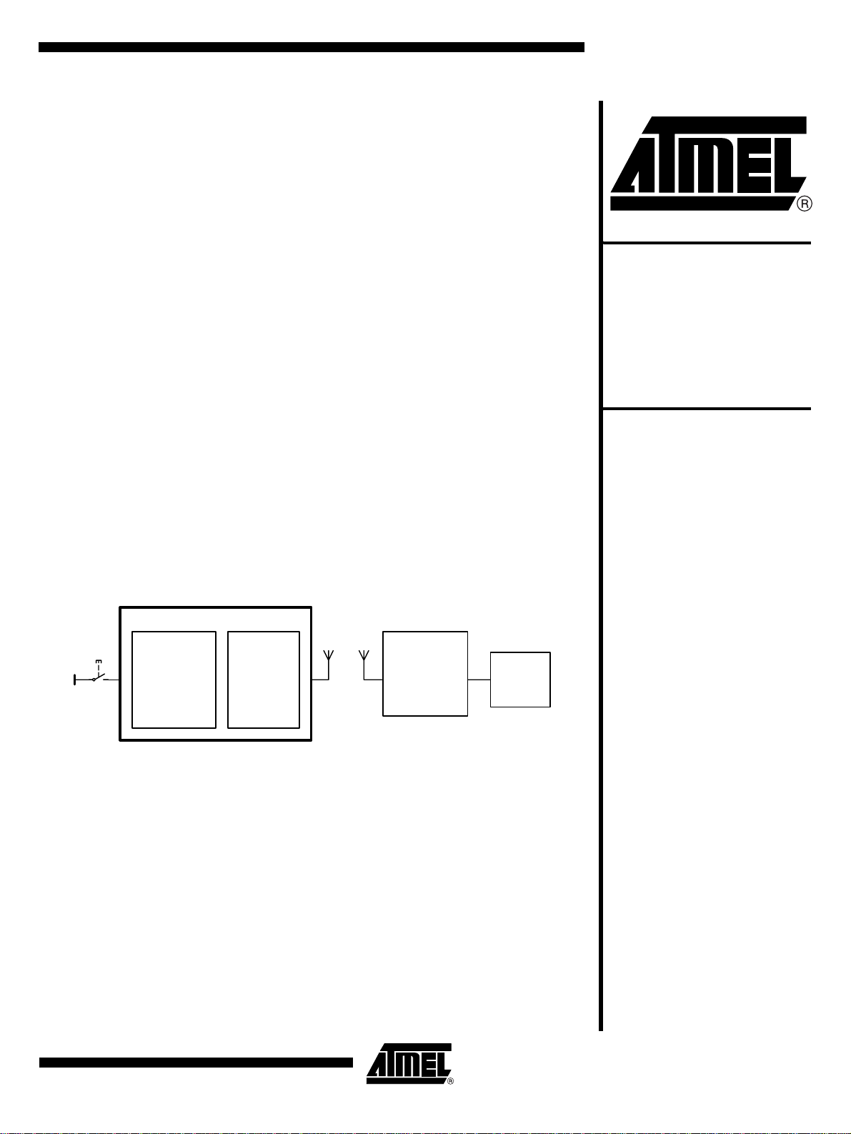
Figure 1. Application Diagram
ATAR862-4
Antenna
UHF ASK/FSK
Receiver
Micro-
controller
Keys
Micro-
controller
PLL-
Transmitter
ASK/FSK
Transmitter
ATAR862-4
Preliminary
Rev. 4552B–4BMCU–02/03
1
Page 2
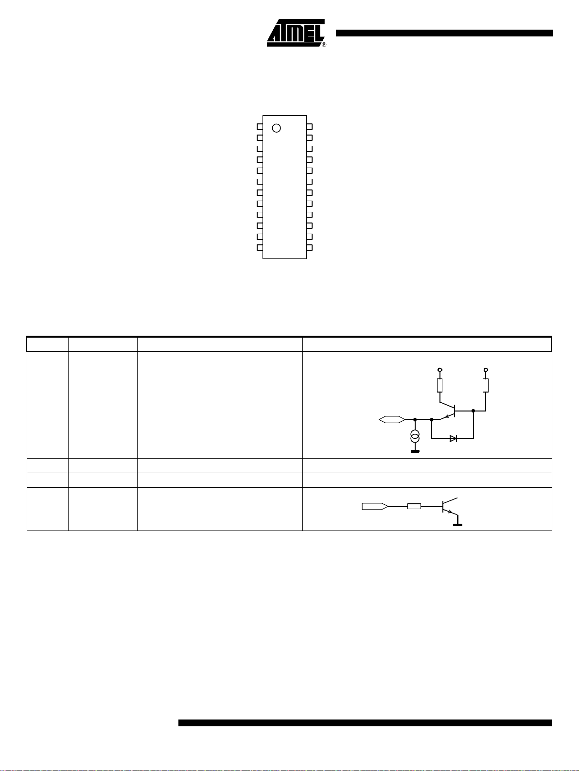
Pin Configuration
Figure 2. Pinning SSO24
XTAL
VS
GND
ENABLE
NRESET
BP63/T3I
BP20/NTE
BP23
BP41/T2I/VMI
BP42/T2O
BP43/SD/INT3
VSS
1
2
3
4
5
6
7
8
9
10
11
12
ANT1
24
ANT2
23
PA_ENABLE
22
CLK
21
BP60/T3O
20
OSC2
19
OSC1
18
BP50/INT6
17
BP52/INT1
16
BP53/INT1
15
BP40/SC/INT3
14
VDD
13
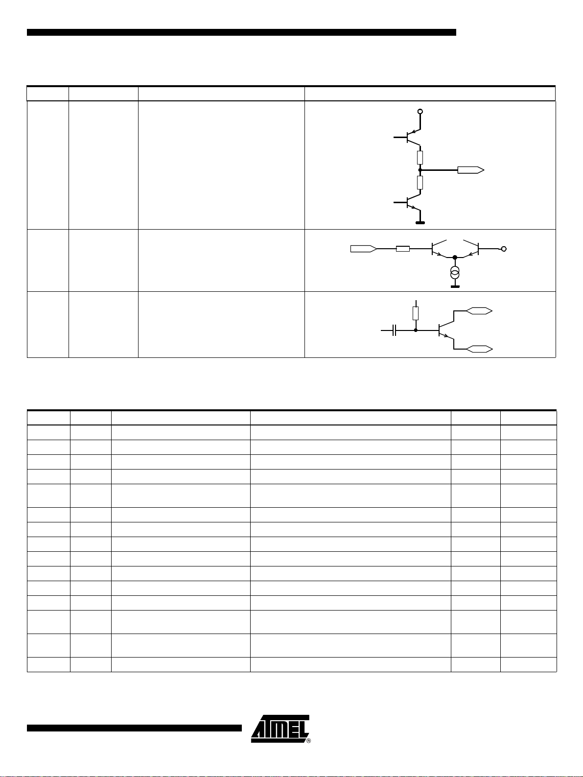
Pin Description: RF Part
Pin Symbol Function Configuration
1 XTAL Connection for crystal
1.5k
VS
VS
1.2k
XTAL
182 mA
2 VS Supply voltage ESD protection circuitry (see Figure 8)
3 GND Ground ESD protection circuitry (see Figure 8)
4 ENABLE Enable input
ENABLE
200k
2
ATAR862-4
4552B–4BMCU–02/03
Page 3
Pin Description: RF Part (Continued)
Pin Symbol Function Configuration
21 CLK Clock output signal for microcontroller
The clock output fre quency is set by the
crystal to f
XTAL
/4
ATAR862-4
VS
100
100
22 PA_ENABLE Switches on power amplifier, used for
ASK modulation
23
24
ANT2
ANT1
Emitter of antenna output stage
Open collector antenna output
PA_ENABLE
50k
20 mA
Pin Description: Microcontroller Part
Name Type Function Alternate Function Pin-No.
V
DD
V
SS
BP20 I/O Bi-directional I/O line of Port 2.0 NTE-test mode enable, see also section "Master Reset" 7
BP40 I/O Bi-directional I/O line of Port 4.0 SC-serial clock or INT3 external interrupt input 14
BP41 I/O Bi-directional I/O line of Port 4.1
BP42 I/O Bi-directional I/O line of Port 4.2 T2O Timer 2 output 10
BP43 I/O Bi-directional I/O line of Port 4.3 S D ser ial data I/O or INT3-external interrupt input 11
BP50 I/O Bi-directional I/O line of Port 5.0 I NT 6 external interrupt input 17
BP52 I/O Bi-directional I/O line of Port 5.2 I NT 1 external interrupt input 16
BP53 I/O Bi-directional I/O line of Port 5.3 I NT 1 external interrupt input 15
BP60 I/O Bi-directional I/O line of Port 6.0 T3O Timer 3 output 20
BP63 I/O Bi-directional I/O line of Port 6.3 T3I Timer 3 input 6
OSC1 I Oscillator input
OSC2 O Oscillator output
NRESET I/O Bi-directional reset pin – 5
– Supply voltage – 13
– Circuit ground – 12
VMI voltage monitor input or T2I external clock input
Timer 2
4-MHz crystal input or 32-kHz crystal input or external
clock input or external trimming resistor input
4-MHz crystal output or 32-kHz crystal output or external
clock input
CLK
ANT1
ANT2
9
18
19
Uref=1.1V
Reset State
NA
NA
Input
Input
Input
Input
Input
Input
Input
Input
Input
Input
Input
Input
I/O
4552B–4BMCU–02/03
3
Page 4

UHF ASK/FSK Transmitter Block
Features
• Integrated PLL Loop Filter
• ESD Protection (4 kV HBM/200 V MM, Except Pin 2: 4 kV HBM/100 V MM) also at ANT1/ANT2
• Maximum Output Power (10 dBm) with Low Supply Current (9.5 mA Typically)
• Modulation Scheme ASK/FSK
– FSK Modulation is Achieved by Connecting an Additional Capacitor between the XTAL Load Capacitor and the Open-
drain Output of the Modulating Microcontroller
• Easy to Design-in Due to Excellent Isolation of the PLL from the PA and Power Supply
• Supply Voltage 2.0 V to 4.0 V in the Temperature Range of -40°C to +125 °C
• Single-ended Antenna Output with High Efficient Pow er Amplifier
• External CLK Output for Clocking the Microcontroller
• 125°C Operation for Tire Pressure Systems
Description
The PLL transmitter block has been developed for the demands of RF low -cost transmission systems, at data rates up to
32 kbaud. The transmitting frequency range is 429 MHz to 439 MHz. It can be used in both FSK and ASK systems.
4
ATAR862-4
4552B–4BMCU–02/03
Page 5
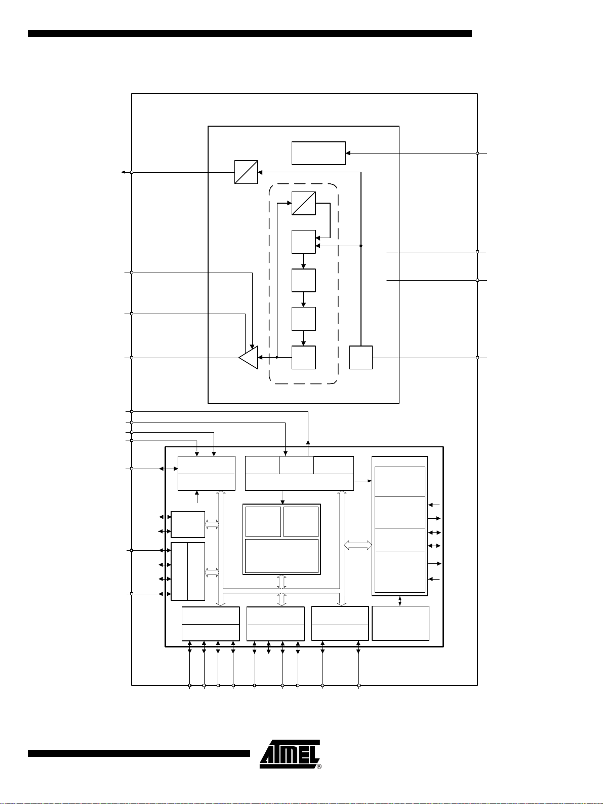
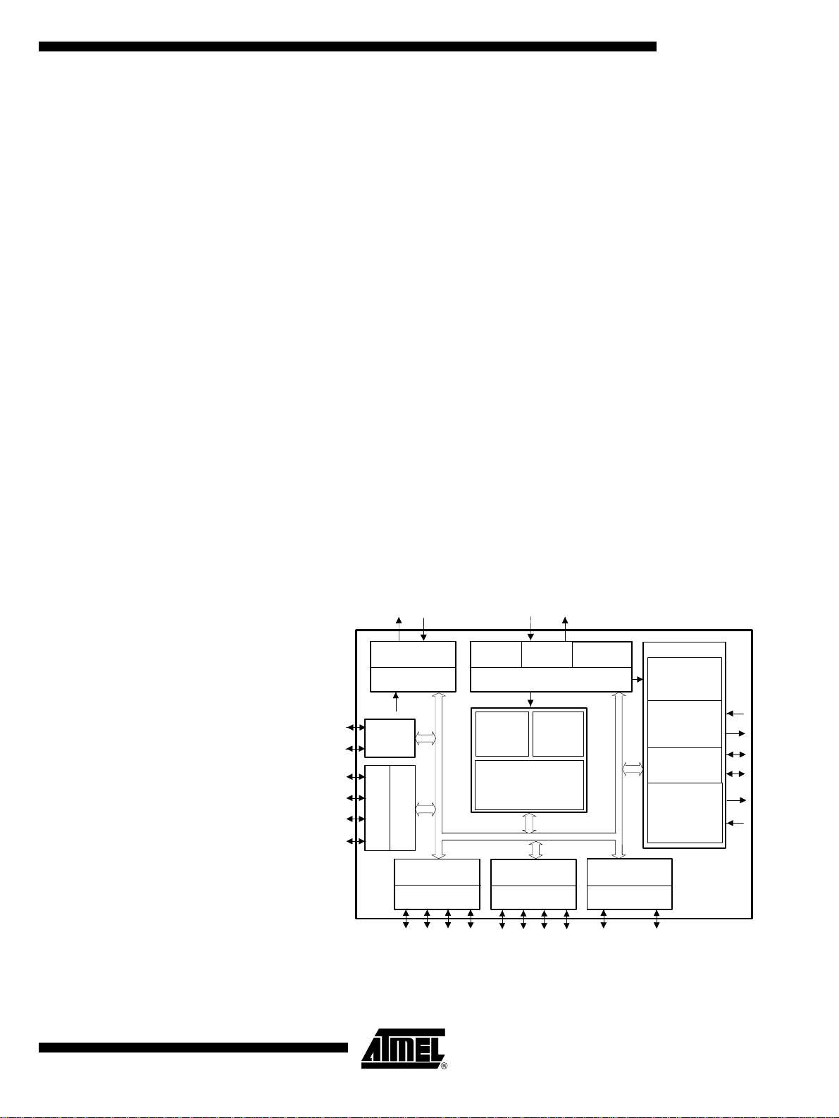
Figure 3. Block Diagram
ATAR862-4
ATAR862-4
CLK
PA_ENABLE
ANT2
ANT1
OSC2
OSC1
V
DD
V
SS
NRESET
BP20/NTE
BP23
BP10
BP13
BP21
BP22
Brown-out protect.
RESET
Voltage monitor
External input
VMI
Port 1
n
o
i
t
c
2
e
t
r
r
i
o
d
P
a
t
a
D
f
4
PA
RC
oscillators
ROM
4 K x 8 bit
4-bit CPU core
Power up /
down
f
32
PFD
CP
LF
VCO
PLL
Crystal
oscillators
Clock management
clock input
RAM
256 x 4 bit
I/O bus
External
XTO
UTCM
Timer 1
interval- and
watchdog timer
Timer 2
8/12-bit timer
with modulator
SSI
Serial interface
Timer 3
8-bit
timer / counter
with modulator
and demodulator
ENABLE
VS
GND
XTAL
µC
T2I
T2O
SD
SC
T3O
T3I
4552B–4BMCU–02/03
Data direction +
alternate function
Port 4
BP40
BP41
INT3
VMI
SC
T2I
BP42
T2O
BP43
INT3
SD
Data direction +
interrupt control
Port 5
BP51
INT6
BP52
BP50
INT1
INT6
BP53
INT1
Data direction +
alternate function
Port 6
BP60
T3O
BP63
T3I
EEPROM
32 x 16 bit
5
Page 6

General Desc ription The fully-integrated PLL transmitter that allows particularly simple, low-cost RF minia-
ture transmitters to be assembled. The VCO is locked to 32 f
crystal is needed for a 433.92 MHz transmitter. All other PLL and VCO peripheral elements are integrated.
The XTO is a series res onance oscillator so that only one capac itor together with a
crystal connected in series to GND are needed as external elements.
The crystal oscillator togethe r with the PLL nee ds maximum < 1 ms unti l the PLL is
locked and the CLK ou tput is sta ble. A wait time of ³ 1 ms until the CLK is used for the
microcontroller and the PA is switched on.
The power amplifier is an open-collector output delivering a current pulse which is nearly
independent from t he load imped ance. The del ivered ou tput power is controlle d via the
connected load impedance.
This output configuration enables a simple matching to any kind of antenna or to 50 W. A
high power efficiency of h =P
an optimized load impedance of Z
out
/(I
S,PA VS
Load
) of 36% for the power amplifier results when
= (166 + j223) W is used at 3 V supply voltage.
, thus, a 13.56 MHz
XTAL
Functional Description
If ENABLE = L and PA_ENABLE = L, the circuit is in standby mode consuming only a
very small amount o f current s o that a li thium cell u sed as po wer supply can work for
several years.
With ENABLE = H, the XTO, PLL and the CLK driver are switched on. If PA_ENABLE
remains L, only the PLL and the XT O are r unn ing and the CLK si gn al is del iver ed to the
microcontroller. The VCO locks to 32 times the XTO frequency.
With ENABLE = H and PA_ENABLE = H, the PLL, XTO, CLK driver and the power
amplifier are on. With PA_ENABLE, the power amplifier can be switched on and off,
which is used to perform the ASK modulation.
ASK Transmission The PLL transmit ter bl oc k is a ct iv ated by ENA BL E = H. PA _E NAB LE m us t r em ain L for
t ³ 1 m s, then the CLK signal can be taken to clock the microcontroller and the output
power can be modulated by means of pin PA_ENABLE. After transmission,
PA_ENABLE is switched to L and the microcontroller switches back to internal clocking.
The PLL transmitter block is switched back to standby mode with ENABLE = L.
FSK Transmission The PLL transmit ter bl oc k is a ct iv ated by ENA BL E = H. PA _E NAB LE m us t r em ain L for
t ³ 1 ms, then the CLK signal can be taken to clock the microcontroller and the power
amplifier is sw itch ed on with PA_ENA BLE = H . The ch ip is then r eady for FSK modul ation. The microcontroller starts to switch on and off the capacitor between the XTAL load
capacitor and GND with an open-drain output port, thus changing the reference frequency of the PLL. If the switch is closed, the output frequency is lower than if the switch
is open. After tra nsmission PA_E NABLE is switch ed to L and the micro controller
switches back to internal clockin g. The PLL transm itter block is switc hed back to
standby mode with ENABLE = L.
The accuracy of the frequency deviation with XTAL pulling method is about ±25% when
the following tolerances are considered.
6
ATAR862-4
4552B–4BMCU–02/03
Page 7
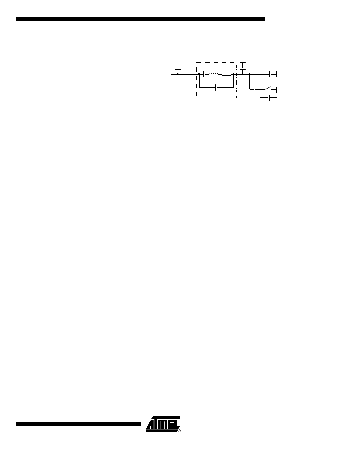
Figure 4. Tolerances of Frequency Modulation
~
V
S
C
XTAL
~
Stray1
CMLMR
Crystal equivalent circuit
C
0
ATAR862-4
C
Stray2
S
C
4
C
5
C
Switch
Using C
capacitances on each side of the crystal of C
capacitance of the crystal of C
=9.2pF ±2%, C5= 6.8 pF ±5%, a switch port with CS
4
= 3.2 pF ±10% and a crystal with CM= 13 fF ±10%, an
0
Stray1=CStray2
=3pF ±10%, stray
witch
= 1 pF ±10%, a para llel
FSK deviation of ± 21 kHz typical with worst case to leranc es of ±16.3 kHz to ±28.8 kHz
results.
CLK Output An output CLK signal is provided for a connected microcontroller. The delivered signal is
CMOS compatible if the load capacitance is lower than 10 pF.
Clock Pulse Take Over The clock of the crystal oscillator can be used for clocking the microcontroller. Atmel’s
M4xCx9x has the special feature of starting with an integrated RC-oscillator to switch on
the PLL transmitter block with ENABLE = H, and after 1 ms to assume the clock signal
of the transmission IC, so the message can be sent with crystal accuracy.
Output Matching and Power Setting
The output power is set by the l oad impe dance o f the ante nna. Th e maximum output
power is achieved with a load impe dance of Z
low resistive path to V
to deliver the DC current.
S
= (166 + j223) W. There must be a
Load,opt
The delivered current pulse of the power amplifier is 9 mA and the maximum output
power is deliver ed to a resistive load of 465 W if the 1.0 pF output capac itance of the
power amplifier is compensated by the load impedance.
An optimum load impedance of:
Z
=465W || j/(2 ´p1.0 pF) = (166 + j223) W thus results for the maximum output
Load
power of 7.5 dBm.
4552B–4BMCU–02/03
The load impedance is def ine d as th e im ped anc e s ee n from the PL L tr ans m itte r blo ck’s
ANT1, ANT2 into the ma tching network . Do not confus e this la rge si gnal load impedance with a small signal input impedance delivered as input characteristic of RF
amplifiers and me asured fr om the appl icatio n into the IC i nstead of from the IC into th e
application for a power amplifier.
Less output power is achieved by lowering the real parallel part of 465 W where the
parallel imaginary part should be kept constant.
Output power measurement can be done with the cir cuit shown in Figure 5. Note that
the component values must be changed to compensate the individual board parasitics
until the PLL transmitter block has the right load impedance Z
= (166 + j223) W.
Load,opt
Also the damping of the cable used to measure the output power must be calibrated.
7
Page 8
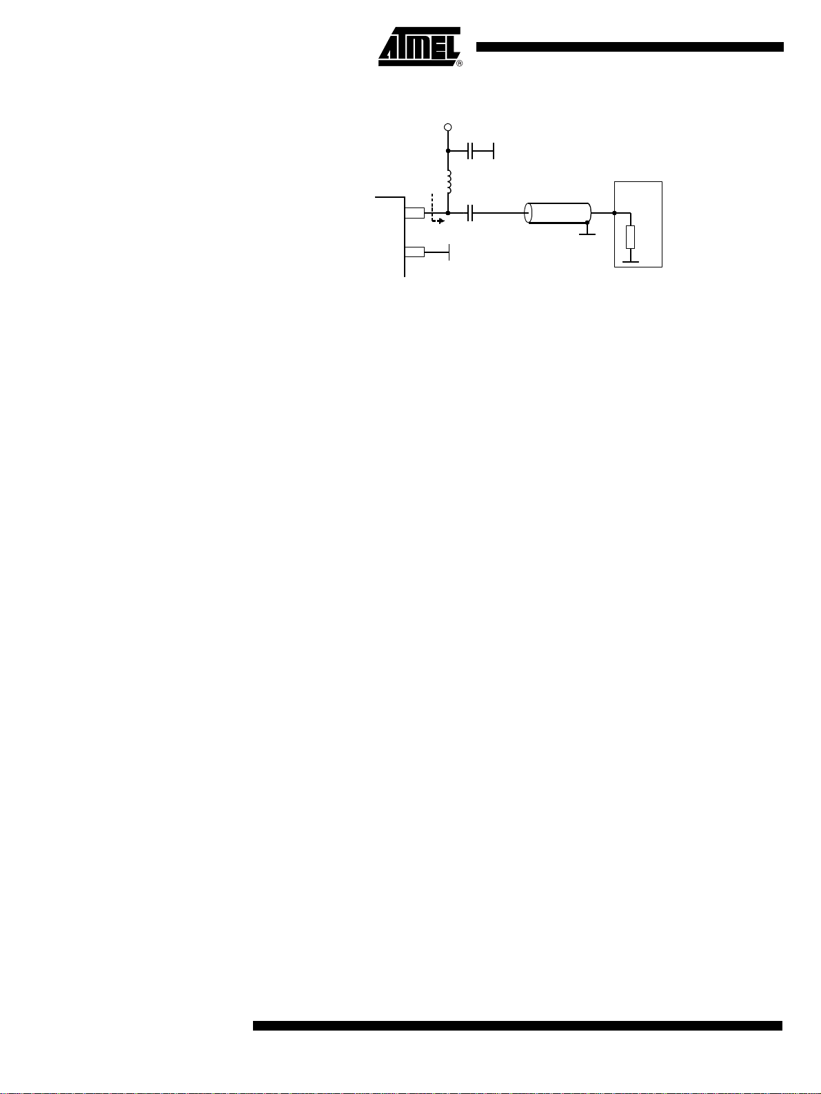
Figure 5. Output Power Measurement
V
S
C1 = 1n
= 33n
L
~
ANT1
Z
ANT2
~
1
C2 = 2.2p
Lopt
Z = 50 W
Power
meter
R
in
50 W
Application Circuit For the supply-voltage blocking capacitor C
(see Figure 6 and Figure 7). C
amplifier where C
for C
two capacitors in series should be used to achieve a better tolerance value and to
2
typically is 8.2 pF/NP0 and C2 is 6 p F/NP0 (10 pF + 15 pF in series);
1
have the possibility to realize the Z
C
forms together with the pins of PLL transmitter block and the PCB board wires a
1
series resonance lo op that supp resses the 1
PCB is important. Normally the best suppression is achieved when C
as possible to the pins ANT1 and ANT2.
The loop antenna should not exceed a width of 1.5 mm, otherwise the Q-factor of the
loop antenna is too high.
L
(50 nH to 100 nH) can be printed on PCB. C4 should be selected so the XTO runs on
1
the load resonance frequency of the crystal. Normally, a value of 12 pF results for a
15 pF load-capacitance crystal.
and C2 are used to match the loop antenna to the power
1
by using standard valued capacitors.
Load,opt
, a value of 68 nF/X7R is recommended
3
st
harmonic, thus, the position of C1 on the
is placed as close
1
8
ATAR862-4
4552B–4BMCU–02/03
Page 9
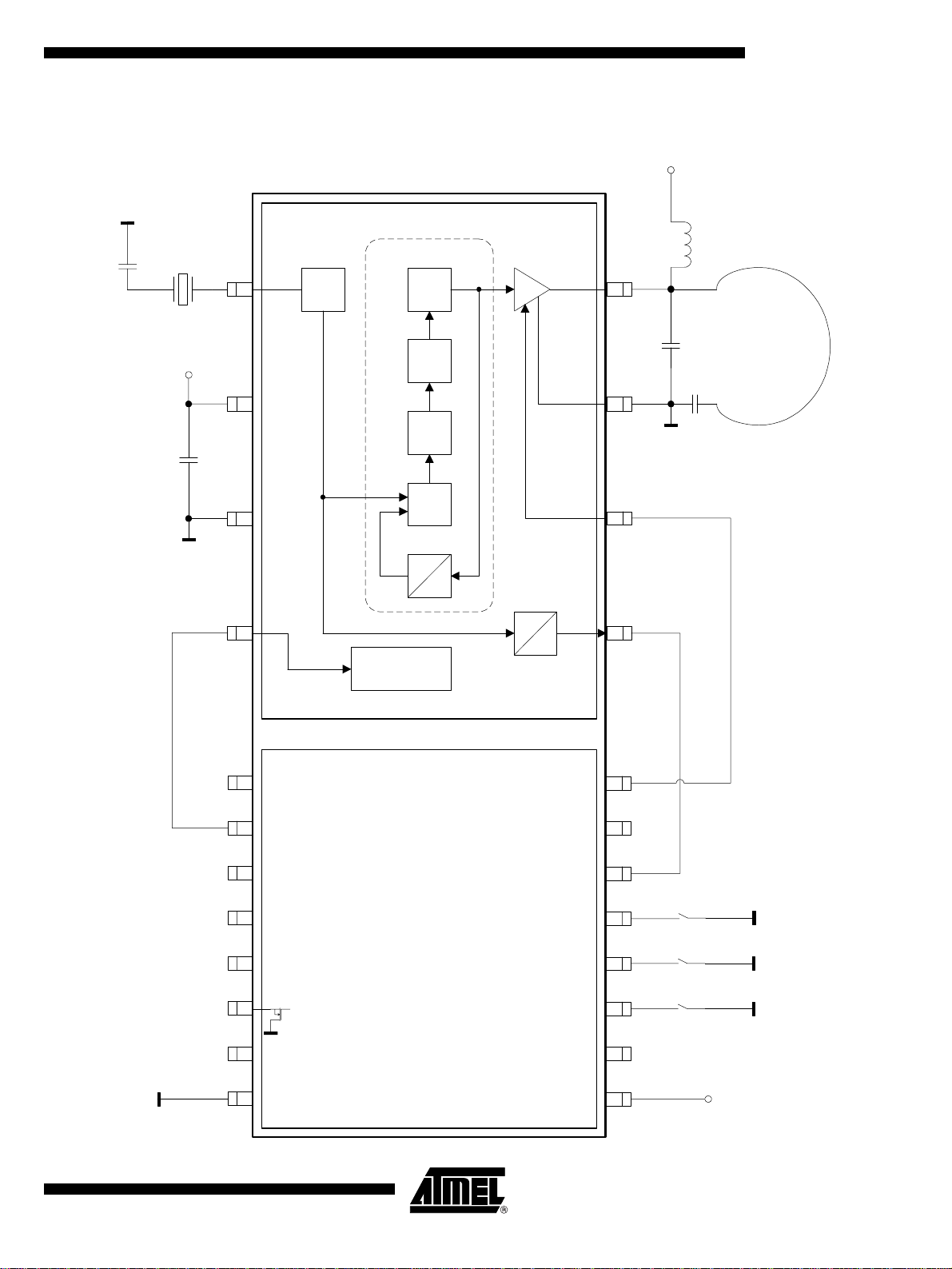
Figure 6. ASK Application Circuit
ATAR862-4
VS
C4
XTAL
VS
XTAL
VS
C3
GND
ENABLE
L1
241
ANT1
23
ANT2
22
PA_ENABLE
21
CLK
C1
Loop
Antenna
C2
PLL
VCO
LF
CP
PFD
32
PA
f
4
f
XTO
2
3
4
Power up/down
4552B–4BMCU–02/03
NRESET
BP63/T3I
BP20/NTE
BP23
BP41/T2I/VMI
BP42/T2O
BP43/SD/
INT3
VSS
10
11
12
5
6
7
8
9
BP60/T3O
20
OSC2
19
OSC1
18
BP50/INT6
17
BP52/INT1
16
BP53/INT1
15
BP40/SC/INT3
17
VDD
13
S1
S2
S3
VS
9
Page 10
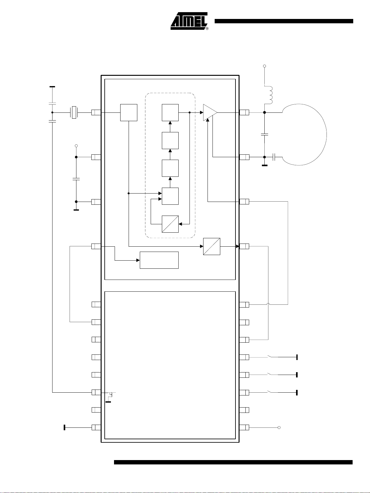
Figure 7. FSK Application Circuit
VS
C4
C5
XTAL
VS
XTAL
VS
C3
GND
ENABLE
L1
241
ANT1
23
ANT2
22
PA_ENABLE
21
CLK
C1
Loop
Antenna
C2
PLL
VCO
LF
CP
PFD
32
PA
f
4
f
XTO
2
3
4
Power up/down
10
NRESET
5
BP63/T3I
BP20/NTE
BP41/T2I/VMI
BP42/T2O
BP43/SD/
INT3
6
7
BP23
8
9
10
11
VSS
12
ATAR862-4
BP60/T3O
20
OSC2
19
OSC1
18
BP50/INT6
17
BP52/INT1
16
BP53/INT1
15
BP40/SC/INT3
17
VDD
13
S1
S2
S3
VS
4552B–4BMCU–02/03
Page 11
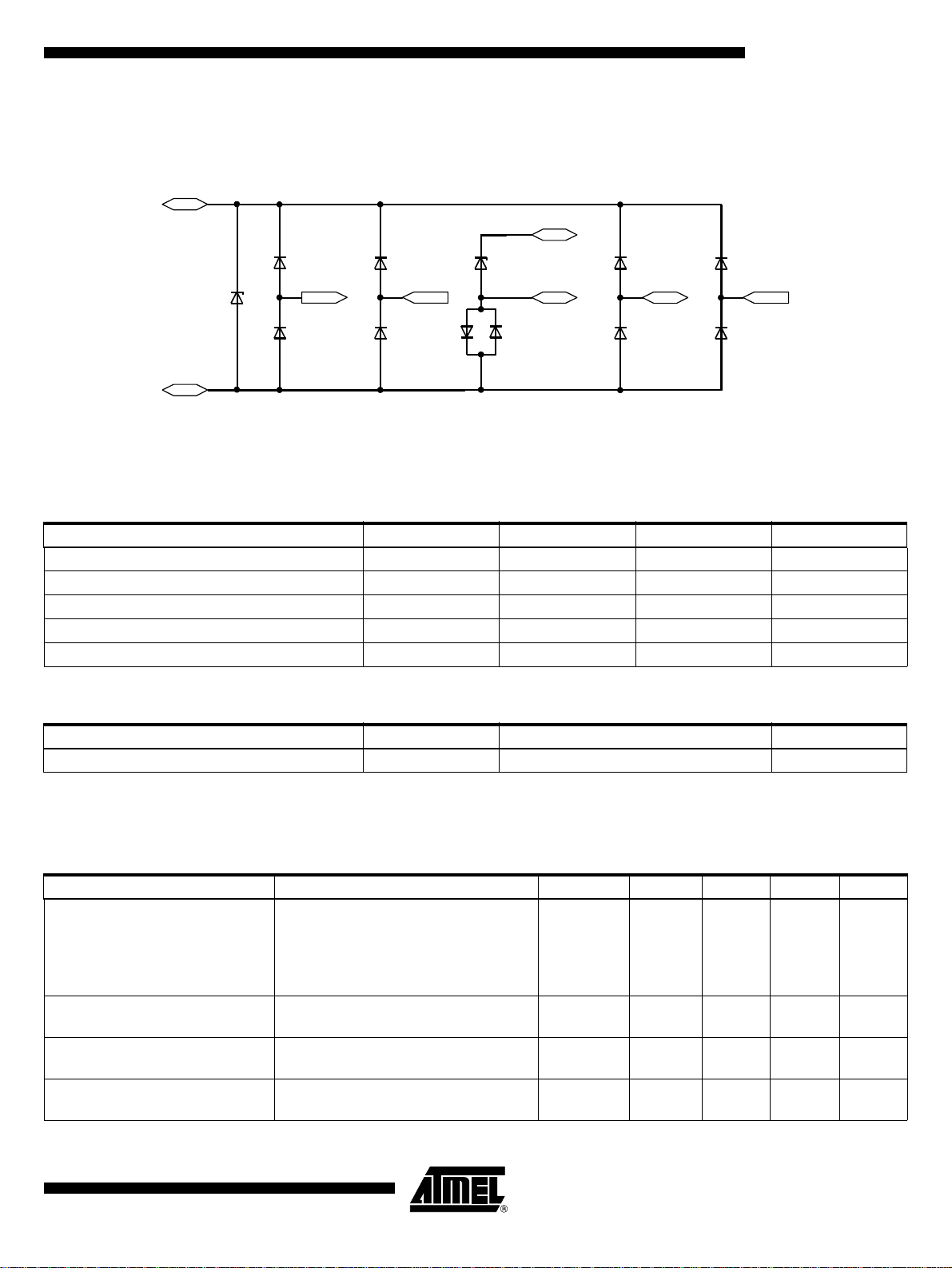
Figure 8. ESD Protection Circuit
VS
ATAR862-4
ANT1
CLK PA_ENABLE
GND
ANT2
XTAL ENABLE
Absolute Maximum Ratings
Parameters Symbol Min. Max. Unit
Supply voltage V
Power dissipation P
Junction temperature T
Storage temperature T
Ambient temperature T
tot
stg
amb
S
j
-55 125 °C
-55 125 °C
5V
100 mW
150 °C
Thermal Resistance
Parameters Symbol Value Unit
Junction ambient R
thJA
170 K/W
Electrical Characteristics
VS = 2.0 V to 4.0 V, T
Typical values are given at V
Parameters Test Conditions Symbol Min. Typ. Max. Unit
Supply current Power down,
Supply current Power up, PA off, VS= 3 V
Supply current Power up, V
Output power VS= 3.0 V, T
4552B–4BMCU–02/03
= -40°C to 125°C unless otherwise specified.
amb
= 3.0 V and T
S
V
ENABLE
V
PA-ENABLE
V
PA-ENABLE
= 25°C. All parameters are referred to GND (Pin 7).
amb
< 0.25 V , -40°C to 85°C
< 0.25 V , -85°C to +125°C
< 0.25 V, 25°C
(100% correlation tested)
ENABLE
ENABLE
> 1.7 V, V
= 3.0 V
S
> 1.7 V, V
amb
V
V
f = 433.92 MHz, Z
PA-EN ABLE
PA-EN ABLE
=25°C
Load
<0.25V
>1.7V
= (166 + j233) W
I
S_Off
I
S
I
S_Transmit
P
Ref
350
7
<10
3.7 4.8 mA
911.6mA
5.5 7.5 10 dBm
nA
µA
nA
11
Page 12

Electrical Characteristics (Continued)
VS = 2.0 V to 4.0 V, T
Typical values are given at V
= -40°C to 125°C unless otherwise specified.
amb
= 3.0 V and T
S
= 25°C. All parameters are referred to GND (Pin 7).
amb
Parameters Test Conditions Symbol Min. Typ. Max. Unit
Output power v ariation for the full
temperature range
Output power v ariation for the full
temperature range
Achievable output-power range Selectable by load impedance P
Spurious emission f
T
= -40°C to +85°C
amb
= 3.0 V
V
S
= 2.0 V
V
S
= -40°C to +125°C
T
amb
V
= 3.0 V
S
= 2.0 V
V
S
= P
P
Out
CLK
Ref
= f0/128
+ DP
Ref
DP
DP
DP
DP
Out_typ
Ref
Ref
Ref
Ref
-1.5
-4.0
-2.0
-4.5
dB
dB
dB
dB
07.5dBm
Load capacitance at Pin CLK = 10 pF
fO ± 1´ f
± 4 ´ f
f
O
CLK
CLK
-55
-52
dBc
dBc
other spurious are lower
Oscillator frequency XTO
(= phase comparator frequency)
f
= f0/32
XTO
= resonant frequency of the
f
XTAL
XTAL, C
£ 10 fF, load capacitance
M
selected accordingly
T
= -40°C to +85°C
amb
= -40°C to +125°C
T
amb
f
XTO
-30
-40
f
XTAL
+30
+40
ppm
ppm
PLL loop bandwidth 250 kHz
Phase noise of phase
comparator
Referred to f
25 kHz distance to carrier
PC
= f
XT0,
-116 -110 dBc/Hz
In loop phase noise PLL 25 kHz distance to carrier -86 -80 dBc/Hz
Phase noise VCO at 1 MHz
at 36 MHz
Frequency range of VCO f
Clock output frequen cy (CMOS
microcontroller compatible)
Voltage swing at Pin CLK C
£ 10 pF V
Load
VCO
0h
V
429 439 MHz
VS´ 0.8
0l
-94
-125
/128 MHz
f
0
V
-90
-121
´ 0.2
S
dBc/Hz
dBc/Hz
V
V
Series resonance R of the c rystal Rs 110 W
Capacitive load at Pin XT0 7pF
FSK modulation frequency rate Duty cycle of the modulation signal =
50%
ASK modulation frequency rate Duty cycle of the modulation signal =
50%
ENABLE input Low level input voltage
High level input voltage
Input current high
PA_ENABLE input Low level input voltage
High level input voltage
Input current high
V
Il
V
Ih
I
In
V
Il
V
Ih
I
In
032kHz
032kHz
0.25
1.7
20
0.25
1.7
5
V
V
µA
V
V
µA
12
ATAR862-4
4552B–4BMCU–02/03
Page 13
Microcontroller Block
ATAR862-4
Features
• Extended Temperature Range for High Temperature up to 125°C
• 4-Kbyte ROM, 256 x 4-bit RAM
• 16 Bi-directional I/Os
• Up to Seven External/Internal Interrupt Sources
• Multifunction Timer/Counter
– IR Remote Control Carrier Generator
– Biphase-, Manchester - and Pulse -w idth Mod ulato r and Demodula tor
– Phase Control Function
• Programmable System Clock with Prescaler and Five Different Clock Sources
• Supply-voltage Range (2.0 V to 4.0 V)
• Very Low Sleep Current (< 1 µA)
• 32 x 16-bit EEPROM (ATAR892 Only)
• Synchronous Serial Interface (2-wire, 3-wire)
• Watchdog, POR and Brown-out Function
• Voltage Monitoring Inclusive Lo_BAT Detect
• Flash Controller T48C862 Available (SSO24)
Description The ATAR862-4 is a member of Atmel’s fami ly of 4-bit single-chip micr ocontrollers. It
offers highest integration for IR and RF data communication, remote-control and phasecontrol applications. The ATAR862-4 is suitable for the transmitter side as well as the
receiver side. It contains ROM, RAM, parallel I/O ports, two 8-bit programmable multifunction timer/co unters with mod ulator and de modulator fun ction, voltag e supervis or,
interval timer with wat chdog fun ction and a soph istic ated on -chip cl ock gene ration with
external clock input, integrated RC-oscillator, 32-kHz and 4-MHz crystal-oscillators. The
ATAR862-4 has an EEPROM as a third chip in one package.
Figure 9. Block Diagram
V
SS
Brown-out prot ect.
RESET
Voltage monitor
External input
VMI
BP10
BP13
BP20/NTE
BP21
BP22
BP23
Port 1
n
o
i
t
c
2
e
t
r
r
i
o
d
P
a
t
a
D
Data direction +
alternate fu nc tion
BP40
INT3
SC BP41
V
DD
Port 4
BP42
T2O
BP43
VMI
T2I SD
INT3
OSC1 OSC2
RC
oscillators
Crystal
oscillators
Clock management
ROM RAM
4 K x 8 bit
MARC4
4-bit CPU core
Data direction +
interrupt control
Port 5
BP51
INT6
BP52
BP50
INT6
256 x 4 bit
INT1
clock input
I/O bus
BP53
INT1
External
Data direction +
alternate function
Port 6
BP60
T3O
UTCM
Timer 1
interval- and
watchdog timer
Timer 2
8/12-bit timer
with modulator
SSI
Serial interface
Timer 3
8-bit
timer / counter
with modulator
and demodulator
BP63
T3I
T2I
T2O
SD
SC
T3O
T3I
4552B–4BMCU–02/03
13
Page 14
Introduction The ATAR8 62-4 is a member of Atmel’s fami ly of 4-bit single-chip mi crocontrollers . It
contains ROM, RAM, parallel I /O ports, two 8-b it programmable m ultifunction
timer/counters, volt age s upervisor , inte rval ti mer wit h watch dog function and a sophi sticated on-chip clock generation with integrated RC-, 32-kHz and 4-MHz crystal
oscillators.
Table 1. Available Variants of M4xCx9x
Version Type ROM E2PROM Peripheral Packages
Flash
device
Production ATAR862 4-Kbyte Mask ROM 64-bytes SSO24
T48C862 4-Kby te EEPR OM 64-bytes SSO24
MARC4 Architecture General Desc ription
The MARC4 microcontroller consists of an advanced stack-based, 4-bit CPU core and
on-chip peripherals . The CPU i s based o n the Harvard ar chit ectur e with ph ysical ly separated program memory (ROM) and data memory (RAM). Three independent buses,
the instruction bus, the memory bus and the I/O bus, are used for parallel communication between ROM, RAM and peripherals. This enhances program execution speed by
allowing both inst ructio n pre fetchi ng, and a si multan eous commu nicat ion to the on -chip
peripheral circuitry. The extremely powerful integr ated interrupt controller with associated eight prioritized interrupt levels supports fast and efficient processing of hardware
events. The MARC4 is designed for the high-level programming language qFORTH.
The core includes both an expressi on and a return stack. This architecture e nables
high-level language programming without any loss of efficiency or code density.
Figure 10. MARC4 Core
MARC4 CORE
SP
RP
CCR
X
Y
RAM
256 x 4-bit
TOS
ALU
Reset
Clock
System
clock
Sleep
Reset
Program
memory
Instruction
bus
Instruction
decoder
Interrupt
controller
PC
Memory bus
I/O bus
Components of MARC4 Core
14
ATAR862-4
On-chip peripheral modules
The core contai ns ROM, RAM, ALU, prog ram cou nter, RAM ad dress r egiste rs, instr uction decoder and interrupt controller. The following sections describe each functional
block in more detail.
4552B–4BMCU–02/03
Page 15
ATAR862-4
ROM The program memory (ROM) is mask programmed with the customer application pro-
gram during the fabrica tion of the micro controller. The ROM is addres sed by a 12-bit
wide program cou nter, thu s pr edefin ing a max imum pr ogram bank s ize of 4 Kbyt es. A n
additional 1-Kbyte of ROM exists, which is rese rved for q ual ity control self-test software
The lowest user ROM address segment is taken up by a 512-bytes Zero page which
contains predefined st art address es for i nterrupt servi ce routines and special subroutines accessible with single byte instructions (SCALL).
The corresponding memory map is shown in Figur e 4. Look-up tab les of consta nts can
also be held in ROM and are accessed via the MARC4’s built-in table instruction.
Figure 11. ROM Map of the Microcontroller Block
1F8h
FFFh
7FFh
1FFh
000h
ROM
(4 K x 8 bit)
Zero page
1F0h
1E8h
1E0h
Zero
page
SCALL addresses
020h
018h
010h
008h
000h
1E0h
1C0h
180h
140h
100h
0C0h
080h
040h
008h
000h
INT7
INT6
INT5
INT4
INT3
INT2
INT1
INT0
$RESET
$AUTOSLEEP
RAM The microcontroller block contains 256 x 4-bit wide static random access memory
(RAM), which is used for the expression stack. The return stack and data memory are
used for variables and arrays. The RAM is addressed by any of the four 8-bit wide RAM
address registers SP, RP, X and Y.
Expression Stack The 4-bit wide expression stack is addressed with the expression stack pointer (SP). All
arithmetic, I/O and memory reference operations take their operands, and return their
results to the expression stack. The MARC4 performs the operations with the top of
stack items (TOS and TOS-1). The TOS register contains the top element of the expression stack and works in the same way as an accumulat or. This stack is als o used for
passing parameters betw een sub routi nes and as a sc ratch pad area for temporary storage of data.
Return Stack The 12-bit wide return stack is ad dr es se d by the re tu rn s tac k p oin ter ( RP ) . It i s us ed for
storing return ad dresses of subr outines, interrupt r outines and for keeping l oop index
counts. The return stack can also be used as a temporary storage area.
The MARC4 instructi on se t s up por ts th e e xc ha nge of da ta b etwe en the top el em ents of
the expression stack and the return stack. The two stacks within the RAM have a user
definable location and maximum depth.
4552B–4BMCU–02/03
15
Page 16
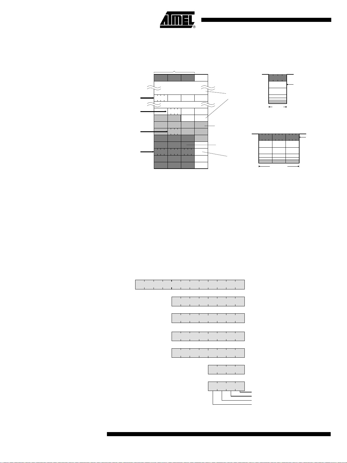
Figure 12. RAM Map
FCh
X
Y
RAM
(256 x 4-bit)
Autosleep
FFh
Global
variables
Expression stack
30
TOS
TOS-1
TOS-2
4-bit
SP
SP
RAM address register:
RP
04h
00h
TOS-1
Expression
stack
Return
stack
07h
03h
Global
v
variables
Return stack
011
RP
12-bit
Registers The microcontroll er ha s se ven p rogramm able regis ters a nd o ne co nditio n cod e reg ister
(see Figure 13).
Program Counter (PC) The program counte r is a 12 -bit reg ister which c ontains th e ad dress o f the nex t inst ruc-
tion to be fetched from the ROM. Instructions currently being executed are decoded in
the instruction decoder to determine the internal micro-operations. For linear code (no
calls or branches), the prog ram counte r is increm ented with every instructio n cycle. If a
branch-, call-, return-instruction or an interrupt is executed, the program counter is
loaded with a new address . The program co unter is also used with the tab le instruc tion
to fetch 8-bit wide ROM constants.
Figure 13. Programming Mode l
PC
11
RP
SP
X
Y
7
7
7
TOS
C
CCR
--
0
Program counter
0
00
Return stack pointer
0
Expression stack pointer
0
RAM address register (X)
07
RAM address register (Y)
03
Top of stack register
03
B
Condition code register
I
Interrupt enable
Branch
Reserved
Carry / borrow
16
ATAR862-4
4552B–4BMCU–02/03
Page 17

ATAR862-4
RAM Address Registers The RAM is addressed with the four 8-bit wide RAM address registers: SP, RP, X and Y.
These registers allow access to any of the 256 RAM nibbles.
Expression Stack Pointer (SP) The stack poi nter conta ins the add ress of the next-to-t op 4-bit it em (TOS-1 ) of the
expression stack. The pointer is automatically pre-incremented if a nibble is moved onto
the stack or post-decremented if a nibble is removed from the stack. Every post-decrement operation moves the item (TOS-1) to the TOS register before the SP is
decremented. Afte r a reset, the stac k pointer ha s to be initia lized with ">SP S0" t o allocate the start address of the expression stack area.
Return Stack Pointer (RP) The return stack pointer points to the top element of the 12-bit wide retur n stack. The
pointer automatically pre-increments if an element is moved onto the stack, or it postdecrements if an element is removed from the stack. The return stack pointer increments and decrements in steps of 4. This means that every time a 12-bit element is
stacked, a 4-bit RAM location is left unwritten. This location is used by the qFORTH
compiler to allocate 4-bit variables. After a reset the return stack pointer has to be initialized via ">RP FCh".
RAM Address Registers (X and Y)
Top of Stack (TOS) The top of stack register is the ac cumul ator of the MA RC4. Al l arit hmetic/lo gic, m emory
Condition Code Register (CCR)
Carry/Borrow (C) The carry/borrow flag indicat es that the bor rowi ng o r car ry ing out of a ri thm eti c logi c unit
Branch (B) The branch flag co ntrol s the con di tio nal progr a m br an ch ing . S hou ld the br anc h flag has
Interrupt Enable (I) The interrupt enable flag globally enables or disables the triggering of all interrupt rou-
The X and Y registers are used to add ress any 4-bit item in the RAM. A fetch ope ratio n
moves the addressed nibble onto the TOS. A store operation moves the TOS to the
addressed RAM location. By using either the pre-increment or post-decrement addressing mode arrays in the RAM can be compared, filled or moved.
reference and I/O operati ons use thi s regis ter. The TOS regis ter rec eives da ta from th e
ALU, ROM, RAM or I/O bus.
The 4-bit wide condition code register contains the branch, the carry and the interrupt
enable flag. The se bits ind icate the curren t stat e of the CPU . The CCR flags are se t or
reset by ALU oper ations. The i nstructions SET_BCF, T OG_BF, CCR! and DI allow
direct manipulation of the condition code register.
(ALU) occurred during the last arithmetic operation. During shift and rotate operations,
this bit is used as a fifth bit. Boolean operations have no effect on the C-flag.
been set by a previous instruction, a conditional branch will cause a jump. This flag is
affected by arithmetic, logic, shift, and rotate operations.
tines with the excepti on of the no n-maska ble rese t. After a rese t or while ex ecuting th e
DI instruction, the interrupt enable flag is reset, thus disabling all interrupts. The core will
not accept any further interrupt requests until the interrupt enable flag has been set
again by either executing an EI or SLEEP instruction.
4552B–4BMCU–02/03
17
Page 18
ALU The 4-bit ALU performs all the arithmetic, logical, shift and rotate operations with the top
two elements of the expression stack (TOS and TOS-1) and returns the result to the
TOS. The ALU operations affects the carry/borrow and branch flag in the condition code
register (CCR).
Figure 14. ALU Zero-address Operations
RAM
SP
TOS-1
TOS-2
TOS-3
TOS-4
TOS
ALU
CCR
I/O Bus The I/O ports and the registers of the peripheral module s ar e I/O mappe d. Al l com mun i-
cation between the c ore a nd th e on -chip per ipher als ta ke place via th e I/O bu s a nd th e
associated I/O control. With the MARC4 IN and OUT instructions, the I/O bus allows a
direct read or write access to one of the 16 primary I/O addresses. More about the I/O
access to the on-chi p pe ripher als i s de scri bed in the s ecti on “P erip heral Modul es". T he
I/O bus is internal and is not accessible by the customer on the final microcontroller
device, but it is use d as the inter face for the MA RC4 emulat ion (see als o the sectio n
“Emulation").
Instruction Set The MARC4 instruction set is optimized for the hi gh level programming language
qFORTH. Many MARC4 instructions are qFORTH words. This enables the compiler to
generate a fast and compact progr am code. The CP U has an inst ructi on pipelin e allowing the controller to prefetch an instruction from ROM at the same time as the present
instruction is being executed. The MARC4 is a zero-address machine, the instructions
contain only the oper ation to be p erfor med an d no so urce or de stina tion ad dress f ields .
The operations are impli citl y pe rf ormed on the data placed on the stack. There are oneand two-byte instructions which are executed within 1 to 4 machine cycles. A MARC4
machine cycle is made up of two system clock cycles (SYSCL). Most of the instructions
are only one byte long and are executed in a single machine cycle. For more information
refer to the “MARC4 Programmer’s Guide".
Interrupt Structure The MARC4 can handle interrupts with eight different priority levels. They can be gener-
ated from the internal and external interrup t sources or by a softwar e interrup t from the
CPU itself. Each interrupt level has a hard-wired priority and an associated vector for the
service routine in the ROM (see Table 1). The programmer can postpone the processing
of interrupts by resetting the interrupt enable flag (I) in the CCR. An interrupt occurrence
will still be registered, but the interrupt routine only started after the I-flag is set. All interrupts can be masked, and the priority individually software configured by programming
the appropriate control register of the interrupting module (see section “Peripheral
Modules").
18
ATAR862-4
4552B–4BMCU–02/03
Page 19
ATAR862-4
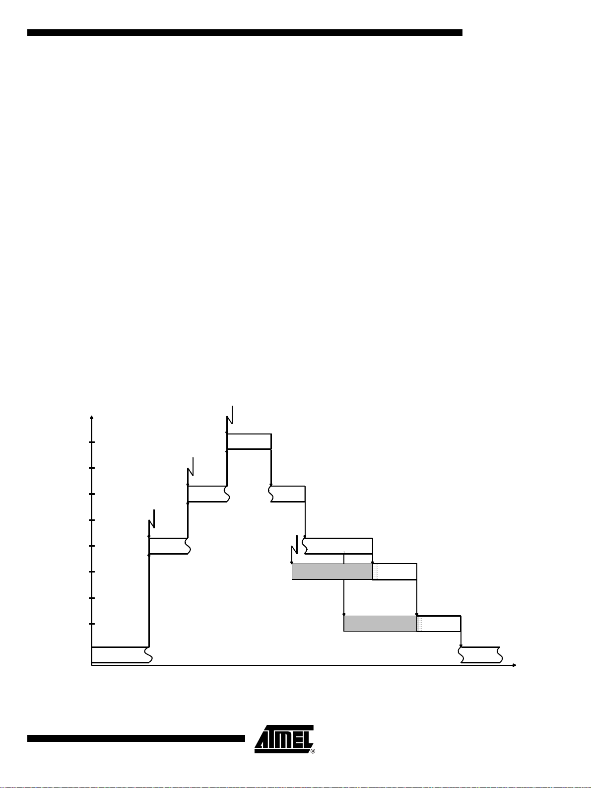
Interrupt Processing For processing the eight interrupt levels, the MARC4 includes an interrupt controller with
two 8-bit wide interrup t pending and inter rupt active registers. The interr upt control ler
samples all interrupt requests during every non-I/O instruction cycle and latches these in
the interrupt pending register. If no higher priority interrupt is present in the interrupt
active register, it signals the CPU to interrupt the current program execution. If the interrupt enable bit is set, the processor enters an interrupt acknowledge cycle. During this
cycle a short call (S CALL) ins truction to the serv ice routin e is exec uted and the current
PC is saved on the return stack. An interrupt service routine is completed with the RTI
instruction. T his inst ruct io n rese ts t he c orres pondi ng b its in t he i nterru pt pendi ng/act ive
register and fetches the return address from th e return stack to the prog ram counter .
When the interrupt enable flag is reset (triggering of interrupt routines is disabled), the
execution of new interrupt service routines is inhibited but not the logging of the interrupt
requests in the inte rrupt pe nding re giste r. The e xecution of the i nterrup t is d elayed u ntil
the interrupt enable flag is set again. Note that interrupts are only lost if an interrupt
request occurs wh ile the corre sponding bi t in the pendin g register is s till set (i.e ., the
interrupt service routine is not yet finished).
It should be noted that automatic stacking of the RBR is not carried out by the hardware
and so if ROM banking is used, the RBR must be stacked on the expression stack by
the application program and res tored before the RTI. After a mast er reset (power-o n,
brown-out or watchdog reset), the interru pt enable flag and the inter rupt pending and
interrupt active register are all reset.
Interrupt Latency The interrupt latenc y is the time from the occurrence of the inte rrup t to th e i nterr upt se r-
vice routine being activated. This is extremely short (taking between 3 to 5 machine
cycles depending on the state of the core).
Figure 15. Interrupt Handling
INT7
7
6
5
4
3
Priority level
2
1
0
Main /
Autosleep
INT5
INT5 active
INT3
INT3 active
INT7 active
RTI
INT2
RTI
INT2 pending
SWI0
INT2 active
INT0 pending
RTI
RTI
INT0 active
RTI
Main /
Autosleep
4552B–4BMCU–02/03
Time
19
Page 20
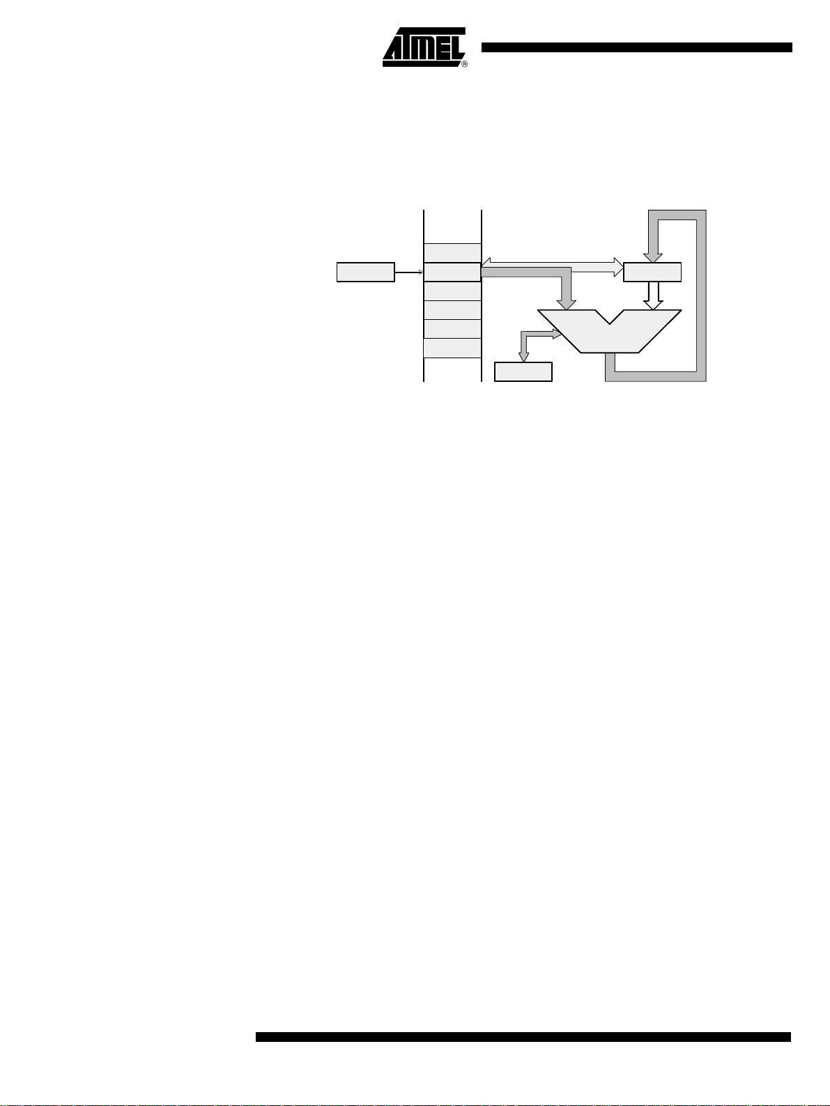
Table 2. Interrupt Priority Table
Interrupt Priority ROM Address Interrupt Opcode Function
INT0 Lowest 040h C8h (SCALL 040h) Software interrupt (SWI0)
INT1 | 080h D0h (SCALL 080h)
INT2 | 0C0h D8h (SCALL 0C0h) Timer 1 interrupt
INT3 | 100h E8h (SCALL 100h)
INT4 | 140h E8h (SCALL 140h) Timer 2 interrupt
INT5 | 180h F0h (SCALL 180h) Timer 3 interrupt
INT6 | 1C0h F8h (SCALL 1C0h)
INT7 Highest 1E0h FCh (SCALL 1E0h) Voltage monitor (VM) interrupt
External hardware interrupt, any edge at BP52 or
BP53
SSI interrupt or external hardware interrupt at BP40
or BP43
External hardware interrupt, at any edg e at BP50 or
BP51
Table 3. Hardware Interrupts
Interrupt Mask
Interrupt
INT1 P5CR
INT2 T1M T 1IM Timer 1
INT3 SISC SIM SSI buffer full/empty or BP40/BP43 interrupt
INT4 T2CM T2IM Timer 2 compare match/overflow
T3CM1
INT5
INT6 P5CR
INT7 VCM VI M External/in ternal v ol tage monitoring
T3CM2
T3C
P52M1, P52M2
P53M1, P53M2
T3IM1
T3IM2
T3EIM
P50M1, P50M2
P51M1, P51M2
Interrupt SourceRegister Bit
Any edge at BP52
any edge at BP53
Timer 3 compare register 1 match
Timer 3 compare register 2 match
Timer 3 edge event occurs (T3I)
Any edge at BP50,
any edge at BP51
Software Interrupts The programmer ca n generate interrupts by using the software interrupt ins truction
(SWI), which is supporte d in qFO RTH by pre defined m acros na med SW I0...SW I7. Th e
software triggered interrupt operates exactly like any hardware triggered interrupt. The
SWI instruction takes the top two elements from the expression stack and writes the corresponding bits via the I/O bus to th e i nter rup t pending register. Therefore, by us in g th e
SWI instruction, interrupts can be re-prioritized or lower priority processes scheduled for
later execution.
Hardware Interrupts In the microcontroller block, there are el even har dw ar e i nterr upt so ur ce s with s eve n d if-
ferent levels. Each source can be masked individually by mask bits in the corresponding
control regi sters. A n overv iew of the po ssible hardwa re conf igurat ions is shown in
Table 3.
20
ATAR862-4
4552B–4BMCU–02/03
Page 21
ATAR862-4
Master Reset The master reset forces the CPU into a well-defined condition. It is unmaskable and is
activated independent of the current program state. It can be triggered by either initial
supply power-up, a short collapse of the power supply, brown-out detection circuitry,
watchdog time-out, or an externa l input cl ock supe rvisor stage (see Figure 9). A mas ter
reset activation will rese t the i nterr upt enab le fl ag, the in ter rupt pe ndi ng r egis ter and th e
interrupt active regi ster. Durin g the power- on reset pha se, the I/O bus contr ol signals
are set to reset m ode, th ereby , init ializi ng al l on- chip periphe rals . All b i-di rection al por ts
are set to input mode.
Attention: During any reset phase, the BP20/NTE input is driven towards V
additional internal strong pull-up transistor. This pin must not be pulled down to V
by an
DD
SS
dur-
ing reset by any external circuitry representing a resistor of less than 150 kW.
Releasing the reset res ults in a sh ort call inst ructi on (opc ode C1h) to the R OM add ress
008h. This activates the initializ ation routine $RESET which in turn has to initia lize all
necessary RAM variables, stack pointers and peripheral configuration registers (see
Table 6).
Figure 16. Reset Configuration
V
DD
Pull-up
CL
NRST
Reset
timer
res
CL=SYSCL/4
Power-on
reset
Brown-out
detection
Internal
reset
V
DD
V
SS
V
DD
V
SS
Po we r-on Reset and Brown-out Detection
4552B–4BMCU–02/03
Watch-
dog
Ext. clock
supervisor
res
CWD
ExIn
The microcontrolle r bloc k has a ful ly in tegr ate d po wer -on r eset an d br own -o ut de tect io n
circuitry. For reset generation no external components are needed.
These circuits ensure that the core is held in the reset state until the minimum operating
supply voltage has been reached. A reset condition will also be generated should the
supply voltage drop momentarily below the minimum operating l evel except when a
power-down mode is activated (the core is in SLEEP mode and the peripheral clock is
stopped). In this power-down mode the brown-out detection is disabled.
Two values for the brown-out voltage threshold are programmable via the BOT-bit in the
SC-register.
21
Page 22
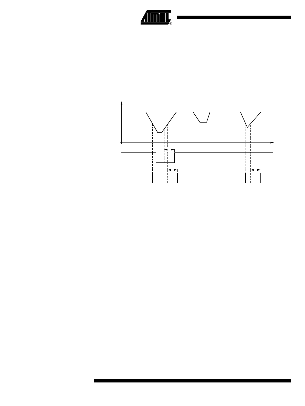
A power-on reset pulse i s generat ed by a VDD rise across the default BOT voltage level
(1.7 V). A brown-out reset pulse is generated when V
falls below the br own-o ut volt -
DD
age threshold. T wo values for t he brown-o ut volt age thres hold are programma ble via
the BOT-bit in the SC-register. When the controller runs in the upper supply voltage
range with a high system clock frequency, the high threshold must be used. When it
runs with a lower system c lock freq uency , the lo w thresho ld and a wider su pply v oltag e
range may be chosen. F or further details , see the e lectrical speci fication and the SCregister description for BOT programming.
Figure 17. Brown-out Detection
V
DD
2.0 V
1.7 V
t
CPU
Reset
CPU
Reset
BOT = '1'
BOT = '0'
d
t
d
t
t
d
td= 1.5 ms (typically)
BOT = 1, low brown-out voltage threshold 1.7 V (is reset value).
BOT = 0, high brown-out voltage threshold 2.0 V.
Watchdog Reset The watchdog’s function can be enabled at the WDC-register and triggers a reset with
every watchdog counter overflow. To suppress the watchdog reset, the watchdog
counter must be regularly reset by reading the watchdog register address (CWD). The
CPU reacts in exactly the same manner as a reset stimulus from any of the above
sources.
External Clock Supervisor The external input clock su per v isor func tion c an be enab led if the ex te rn al inpu t cl oc k is
selected within the CM- and SC-reg isters of the clock module . Th e CPU reacts in
exactly the same manner as a reset stimulus from any of the above sources.
Voltage Monitor The voltage monitor consists of a comparator with internal voltage reference. It is used
to supervise the supply voltage or an external voltage at the VMI-pin. The comparator
for the supply voltage has three internal programmable thresholds one lower threshold
(2.2 V), one middle threshold (2.6 V) and one higher threshold (3.0 V). For external voltages at the VMI-pin, the comparator threshold is set to V
indicates if the supervised voltage is below (VMS = 0) or above (VMS = 1) this threshold. An interrupt can be g enerated wh en the V MS-b it is set or res et to de tect a risin g or
falling slope. A voltage monitor interrupt (INT7) is enabled when the interrupt mask bit
(VIM) is reset in the VMC-register.
= 1.3 V. The VMS-bit
BG
22
ATAR862-4
4552B–4BMCU–02/03
Page 23
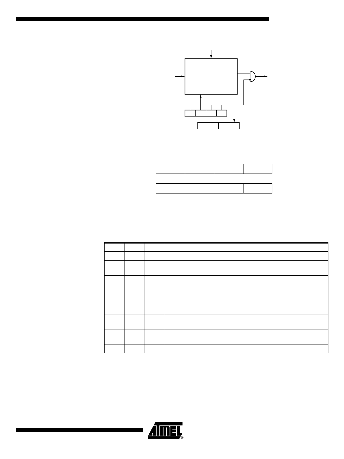
Figure 18. Voltage Monitor
BP41/
VMI
VMC :
Voltage monitor
IN
VM2
VM1 VM0 VIM
ATAR862-4
V
DD
OUT
INT7
Voltage Monitor Control/ Status Register
VMST :
- - res
VMS
Primary register address: "F’hex"
Bit 3Bit 2Bit 1Bit 0
VMC: Write VM2 VM1 VM0 VIM Reset value: 1111b
VMST: Read – – reserved VMS Reset value: xx11b
VM2: Voltage monitor Mode bit 2
VM1: Voltage monitor Mode bit 1
VM0: Voltage monitor Mode bit 0
VM2 VM1 VM0 Function
1 1 1 Disable voltage monitor
110
101Not allowed
100
011
010
001
000Not allowed
External (VIM-input), internal reference thresho ld (1.3 V), interrupt
with negative slope
External (VMI-input), internal reference thresho ld (1.3 V), interrupt
with positive slope
Internal (supply voltage), high threshold (3.0 V), interrupt with
negative slope
Internal (supply voltage), middle threshold (2.6 V), interrupt with
negative slope
Internal (supply voltage), low threshold (2.2 V), interrupt with
negative slope
4552B–4BMCU–02/03
VIM Voltage Interrupt Mask bit
VIM = 0, voltage monitor interrupt is enabled
VIM = 1, voltage monitor interrupt is disabled
VMS Voltage Monitor Status bit
VMS = 0, the voltage at the comparator input is below V
VMS = 1, the voltage at the comparator input is above V
Ref
Ref
23
Page 24

Figure 19. Internal Supply Voltage Supervisor
Low threshold
VMS = 1
V
DD
3.0 V
2.6 V
2.2 V
Middle threshold
High threshold
Low threshold
Middle threshold
High threshold
VMS = 0
Figure 20. External Input Voltage Supervisor
VMI
Negative slope
VMS = 1
1.3 V
VMS = 0
Positive slope
Internal reference level
Interrupt positive slope
VMS = 1
VMS = 0
Interrupt negative slope
t
Clock Generation
Clock Module The microcontroller block contains a clock module with 4 different internal osc illator
types: two RC-oscillators, one 4-MHz crystal oscillator and one 32-kHz crystal oscillator.
The pins OSC1 and OSC2 are the interf ace to c onnect a crysta l either to th e 4-MHz, or
to the 32-kHz crystal oscillator. OSC1 can be used as input for external clocks or to connect an external tri mming res isto r for the R C-o scill ator 2. All ne cess ary ci rcuitr y, exce pt
the crystal and the t rimm ing r esis tor, i s i nte grated on -chi p. O ne of t hes e o scil lat or ty pes
or an external input clock can be selected to generate the system clock (SYSCL).
24
ATAR862-4
In applications that do not require exact timing, it is possible to use the fully integrated
RC-oscillator 1 without any external components. The RC-oscillator 1 center frequency
tolerance is better than ± 50%. The RC-oscillator 2 is a trimmable oscillator whereby the
oscillator frequency can be trimmed with an external resistor attached between OSC1
and V
. In this configuration, the RC-oscillator 2 frequency can be maintained stable
DD
with a tolerance of ± 15% over the full operating temperature and voltage range.
The clock module is programmable via software with the clock management register
(CM) and the system configuration register (SC). The requir ed oscillator c onfiguration
can be selected with the OS1-bit and the OS0-bit in the SC-register. A programmable
4-bit divider stage allows the adjustment of the system clock speed. A special feature of
the clock management is that an external oscillator may be used and switched on and
off via a port pin for the power-down mode. Before the external clock is switched off, the
internal RC-oscillator 1 must be s elected with the CCS-bit and then the SLEE P mode
may be activated. In this state an interrupt can wake up the controller with the RC-oscillator, and the external oscillator can be activated and selected by software. A
synchronization stage avoids too short clock periods if the clock source or the clock
speed is changed. If an external input clock is selected, a supervisor circuit monitors the
external input and gen er ate s a har dwa re reset if the external clock sou rce f ail s or dr ops
below 500 kHz for more than 1 ms.
4552B–4BMCU–02/03
Page 25
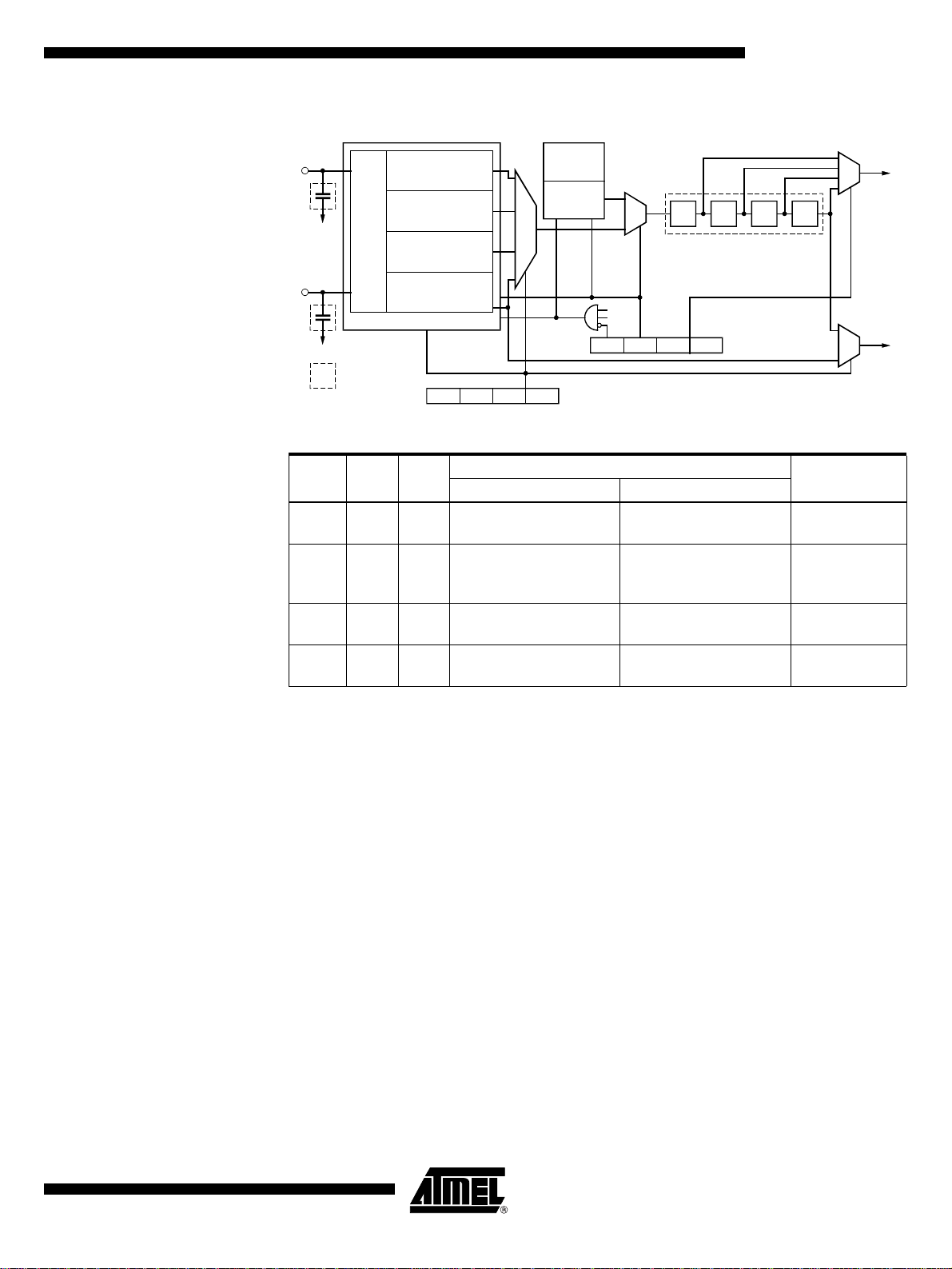
Figure 21. Clock Module
ATAR862-4
OSC1
OSC2
*
*
*
mask option
Oscin
Oscout
Ext. clock
ExIn
RC oscillator2
R
Trim
4-MHz oscillator
Oscin
Oscout
32-kHz oscillator
Oscin
Oscout
BOT - - - OS1 OS0
SC:
Table 4. Clock Modes
Mode OS1 OS0
111
201
310
400
ExOut
Stop
RCOut2
Stop
4Out
Stop
32Out
RC-oscillator 1
(internal)
RC-oscillator 1
(internal)
RC-oscillator 1
(internal)
RC-oscillator 1
(internal)
RC
oscillator 1
IN1
Osc-Stop
RCOut1
ControlStop
NSTOP CCS CSS1 CSS0CM:
IN2
Sleep
WDL
Cin
/2 /2 /2 /2
Clock Source for SYSCL
External input clock C
RC-oscillator 2 with
external trimming
resistor
4-MHz oscillator C
32-kHz oscillator 32 kHz
Divider
SYSCL
Cin/16
32 kHz
SUBCL
Clock Source
for SUBCLCCS = 1 CCS = 0
/16
in
C
/16
in
/16
in
Oscillator Circuits and External Clock Input Stage
RC-oscillator 1 Fully Integrated
The clock module generates two output clocks. One is the system clock (SYSCL) and
the other the periphery (SUBCL). The SYSCL can supply the core and the peripherals
and the SUBCL can supply only the peripherals with cloc ks. The modes for clock
sources are programmable with the OS1-bit and OS0-bit in the SC-register and the
CCS-bit in the CM-regi ste r.
The microcontroller block se ries consi sts of fou r different in ternal os cillators: t wo RCoscillators, one 4-MHz crystal oscillator, one 32-kHz crystal oscillator and one external
clock input stage.
For timing insensitive applications, it is possible to use the fully integrated RC
oscillator 1. It operates without any external components and saves additional costs.
The RC-oscillator 1 center frequency tolerance is better than ±50% over the full temperature and voltage range. The bas ic center frequency of the RC-oscillato r 1 is
f
» 3.8 MHz. The RC oscillator 1 is selected by default after power-on reset.
O
4552B–4BMCU–02/03
25
Page 26
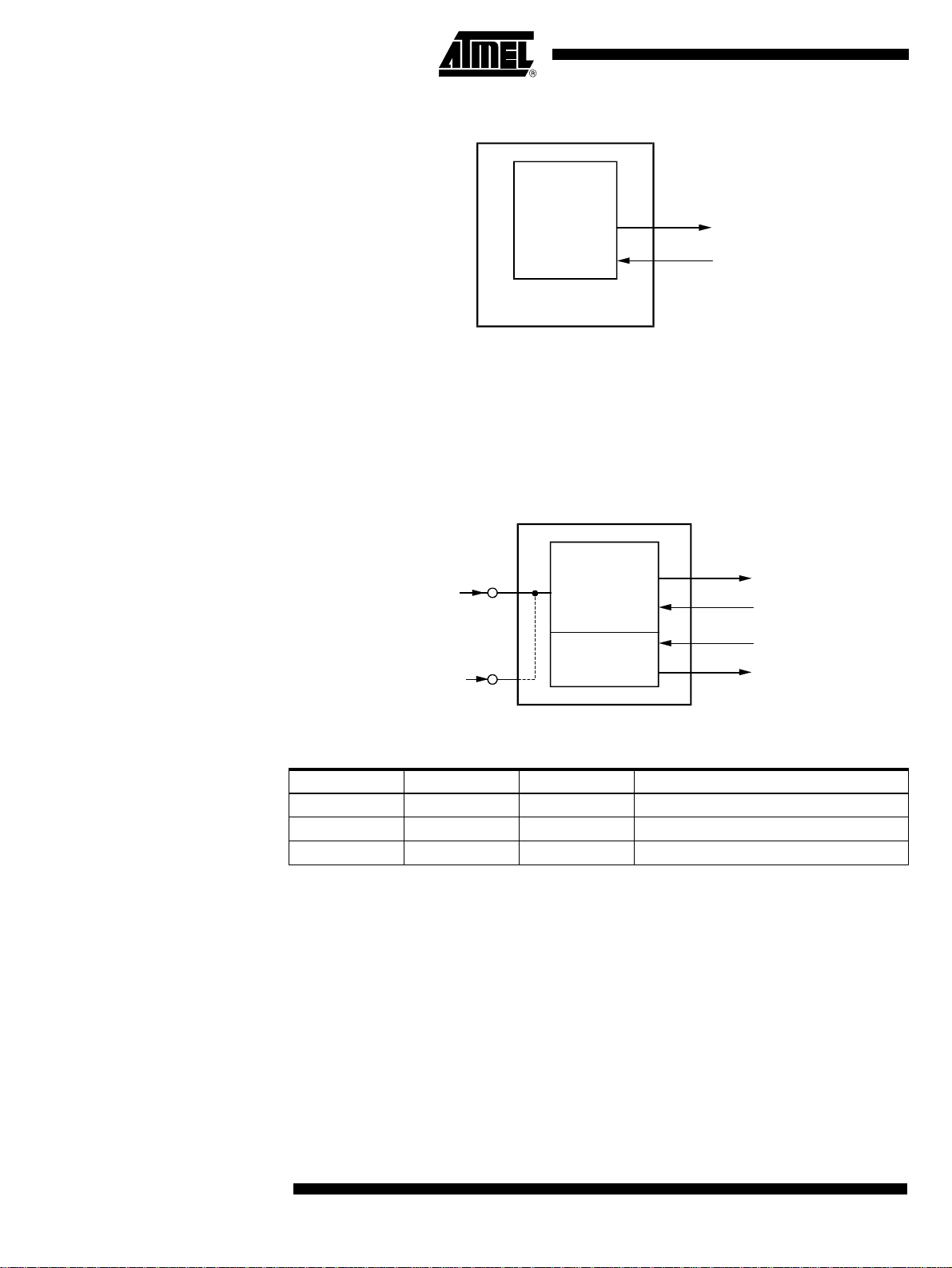
Figure 22. RC-oscillator 1
RC
oscillator 1
RcOut1
Stop
Control
RcOut1
Osc-Stop
External Input Clock The OSC1 or OSC2 (mask option) can be driven by an external clock source provided it
meets the specified duty cycle, rise and fall times and input level s. Additionally, the
external clock stage conta ins a superv isory circuit for the input clock . The supervi sor
function is controlled via the OS1, OS0-bit in the SC-register and the CCS-bit in the CMregister. If the external input clock is missing for more than 1 ms and CCS = 0 is set in
the CM-register, the supervisory circuit generates a hardware reset.
Figure 23. External Input Clock
RC-oscillator 2 with External Trimming Resistor
Ext. input clock
OSC1
Ext.
Clock
or
OSC2
Ext.
Clock
OS1 OS0 CCS Supervisor Reset Output (Res)
110 Enable
111 Disable
x 0 x Disable
ExIn
Clock monitor
ExOut
Stop
RcOut1
Osc-Stop
CCS
Res
The RC-oscillator 2 is a high resolution trimmable oscillator whereby the oscillator frequency can be tri mmed with an exte rnal resistor betw een OSC1 and V
. In this
DD
configuration, the RC-oscillator 2 frequency can be maintained stable with a tolerance of
± 10% over the full operating temperature and a voltage range V
from 2.5 V to 6.0 V.
DD
For example: An output frequency at the RC-oscillator 2 of 2 MHz can be obtained by
connecting a resistor R
=360kW (see Figure 16).
ext
26
ATAR862-4
4552B–4BMCU–02/03
Page 27
ATAR862-4
Figure 24. RC-oscillator 2
V
DD
R
ext
OSC1
OSC2
4-MHz Oscillator The microcontroller block 4-MHz oscillator options need a crystal or ceramic resonator
connected to the OSC1 and OSC2 pins to establish oscillation. All the necessary oscillator circuitry is integrated, except the actual crystal, resonator, C3 and C4.
4-MHz Crystal Oscillator
RC
oscillator 2
R
Trim
RcOut2
Stop
RcOut2
Osc-Stop
OSC1
XTAL
4 MHz
OSC2
*
mask option
Figure 25. Ceramic Resonator
C3
OSC1
OSC2
C4
*
mask option
Cer.
Res
*
C1
*
C2
*
C1
*
C2
Oscin
4-MHz
oscillator
Oscout
Oscin
oscillator
Oscout
4-MHz
4Out
Stop
4Out
Stop
4Out
Osc-Stop
4Out
Osc-Stop
32-kHz Oscillator Some appli catio ns requ ire long- term tim e kee ping o r lo w res olution t iming . In thi s c ase,
an on-chip, low power 32-kHz cr ystal oscillator can be use d to generate both the
SUBCL and the SYSCL. In this mode, power consumption is greatly reduced. The
32-kHz crystal oscillator can not be stopped while the power-down mode is in operation.
27
4552B–4BMCU–02/03
Page 28
Figure 26. 32-kHz Crystal Oscillator
OSC1
XTAL
32 kHz
OSC2
*
mask option
*
C1
*
C2
Oscin
32-kHz
oscillator
Oscout
32Out
32Out
Clock Management The clock management register controls the system clock divider and synchronization
stage. Writing to this register triggers the synchronization cycle.
Clock Management Register (CM)
Bit 3 Bit 2 Bit 1 Bit 0
CM: NSTOP CCS CSS1 CSS0 Reset value: 1111b
Auxiliary register address: "3"hex
NSTOP Not STOP peripheral clock
NSTOP = 0, stops the peripheral clock while the core is in SLEEP mode
NSTOP = 1, enables the peripheral clock while the core is in SLEEP mode
CCS Core Clock Select
CCS = 1, the internal RC-oscillator 1 generates SYSCL
CCS = 0, the 4-MHz crystal oscillator, the 32-kHz crystal oscillator, an external
clock source or the internal RC-oscillator 2 with the external resistor at OSC1
generates SYSCL dependent on the setting of OS0 and OS1 in the system
configuration register
CSS1 Core Speed Select 1
CSS0 Core Speed Select 0
CSS1 CSS0 Divider Note
0016–
1 1 8 Reset value
104–
012–
28
ATAR862-4
4552B–4BMCU–02/03
Page 29
ATAR862-4
System Configuration Register (SC)
Primary register address: "3"hex
Bit 3Bit 2Bit 1Bit 0
SC: write BOT – OS1 OS0 Reset value: 1x11b
BOT Brown-Out Threshold
BOT = 1, low brown-out voltage threshold (1.7 V)
BOT = 0, high brown-out voltage threshold (2.0 V)
OS1 Oscillator Select 1
OS0 Oscillator Select 0
Mode OS1 OS0 Input for SUBCL Selected Oscillators
111 C
201 C
310 C
400 32 kHz
Note: If bit CCS = 0 in the CM-register, the RC-oscillator 1 always stops.
16 RC-oscillator 1 and external input clock
in/
/16 RC-oscillator 1 and RC-oscillator 2
in
/16
in
RC-oscillator 1 and 4-MHz crystal
oscillator
RC-oscillator 1 and 32-kHz crystal
oscillator
Power-down Modes The sleep mode is a shut-down condition which is used to reduce the average system
power consumption in applications where the microcontroller is not fully utilized. In this
mode, the system clock is stopped. The sleep mode is entered via the SLEEP instruction. This instruction sets the interrupt enable bit (I) in the condition code register to
enable all interrup ts and stops the core. Durin g the sleep mode the periphe ral modules
remain active and are able to gene rate interrupt s. The microco ntroller exits the s leep
mode by carrying out any interrupt or a reset.
The sleep mode c an only be kept whe n none of th e interr upt pend ing or ac tive re gister
bits are set. The application of the $AUTOSLEEP routine ensures the correct function of
the sleep mode. For standard applications use the $AUTOSLEEP r outine to enter the
power-down mode. Using the S LE EP in str uc tion i ns tea d of th e $A UTO SLE E P follo win g
an I/O instruction requ ires to ins ert 3 non-I/O inst ructi on cyc les (for exam ple N OP N OP
NOP) between the IN or OUT command and the SLEEP command.
The total power consumption is directly proportional to the active time of the microcontroller. For a rough estimation of the expected average system current consumption, the
following formula should be used:
I
(VDD,f
total
IDD depends on VDD and f
syscl
) = I
syscl
+ (IDD ´ t
Sleep
active/ttotal
)
4552B–4BMCU–02/03
29
Page 30

The microcontroller block has various power-down modes. During the sleep mode the
clock for the MARC4 core is stopped. With the NSTOP-bit in the clock management register (CM), it is programmable if the clock for the on-chip peripherals is active or stopped
during the slee p mode. I f the cl ock for t he core a nd the pe ripheral s is stop ped, the
selected oscillator is switched off. An exception is the 32-kHz oscillator, if it is selected it
runs continuously independent of the NSTOP-bit. If the oscillator is stopped or the
32-kHz oscillator is selected, power consumption is extremely low.
Table 5. Power-down Modes
RC-oscillator 1
Brown-
CPU
Mode
Active RUN NO Active RUN RUN YES
Power-
down
SLEEP SLEEP YES STOP STOP RUN STOP
Note: 1. Osc-Stop = SLEEP and NSTOP and WDL
Core
SLEEP NO Active RUN RUN YES
Osc-
Stop
(1)
out
Function
RC-oscillator 2
4-MHz
Oscillator
32-kHz
Oscillator
External
Input
Clock
Peripheral Modules
Addressing Peripheral s Accessing the peripheral modules takes place via the I/O bus (see Figure 20). The IN or
OUT instructions allow direct addressing of up to 16 I/O modul es. A dual register
addressing scheme has be en ado pted to ena ble dir ect a ddressi ng of the prim ary regi ster. To address the auxiliary register, the access must be switched with an auxiliary
switching m odul e. Thu, s a si ngle IN (or OU T) to the module address will read (or write
into) the module primar y register . Accessin g the auxili ary registe r is perform ed with the
same instruction preceded by writing the module address into the auxiliary switching
module. Byte wide registers are accessed by multiple IN- (or OUT-) instructions. For
more complex peripheral modules, with a larger number of registers, extended addressing is used. In this case, a bank of up to 16 subport registers are indirectly addressed
with the subport address. The first OUT-instruction writes the subport address to the
subaddress register, the second IN- or OUT-instruction reads data from or writes data to
the addressed subport.
30
ATAR862-4
4552B–4BMCU–02/03
Page 31

Figure 27. Example of I/O Addressing
ATAR862-4
Module ASW
Auxiliary Switch
Module
Primary Reg.
Example of
qFORTH
program code
Module M1
(Address Pointer)
Subaddress Reg.
1
Indirect Subport Access
(Subport Register Write)
1 Addr. (SPort) Addr. (M1) OUT
2 SPort _Data Addr. (M1) OUT
(Subport Register Read)
1 Addr. (SPort) Addr. (M1) OUT
2 Addr. (M1) IN
(Subport Register Write Byte)
1 Addr. (SPort) Addr. (M1) OUT
2 SPort _Data(lo) Addr. (M1) OUT
2 SPort _Data(hi) Addr. (M1) OUT
(Subport Register Read Byte)
1 Addr. (SPort) Addr. (M1) OUT
2 Addr. (M1) IN (hi)
2 Addr. (M1) IN (lo)
Bank of
Primary Reg.
Subport Fh
Subport Eh
Subport 1
Subport 0
2
Module M2 Module M3
Aux. Reg.
5
Primary Reg.
3
4
I/O bus
Dual Register Access
(Primary Register Write)
3 Prim._Data Addr. (M2) OUT
(Auxiliary Register Write)
4 Addr. (M2) Addr. (ASW) OUT
5 Aux._Data Addr. (M2) OUT
(Primary Register Read)
3 Addr. (M2) IN
(Auxiliary Register Read)
4 Addr. (M2) Addr. (ASW) OUT
5 Addr. (M2) IN
(Auxiliary Register Write Byte)
4 Addr. (M2) Addr. (ASW) OUT
5 Aux._Data (lo) Addr. (M2) OUT
5 Aux._Data (hi) Addr. (M2) OUT
Primary Reg.
6
to other modules
Single Register Access
(Primary Register Write)
6 Prim._Data Addr.(M3) OUT
(Primary Register Read)
6 Addr. (M3) IN
Addr.(ASW) = Auxiliary Switch Module address
Addr.(Mx) = Module Mx address
Addr.(SPort) = Subport address
Prim._Data = Data to be written into Primary Register
Aux._Data = Data to be written into Auxiliary Register
Prim._Data(lo)= Data to be written into Auxiliary Register (low nibble)
4552B–4BMCU–02/03
Prim._Data(hi) = Data to be written into Auxiliary Register (high nibble)
SPort_Data(lo) = Data to be written into SubPort (low nibble)
SPort_Data(hi) = Data to be written into SubPort (high nibble)
(lo) = SPort_Data (low nibble)
(hi) = SPort_Data (high nibble)
31
Page 32
Table 6. Peripheral Address es
Port Address Name
1 P1DAT W/R 1xx1b Port 1 - data register/input data M3
2 P2DAT W/R 1111b Port 2 - data register/pin data M2
Auxiliary P2CR W 1111b Port 2 - control register M2
3 SC W 1x11b System configuration regist er M 3
CWD R xxxxb Watchdog reset M3
Auxiliary CM W/R 1111b Clock management register M2
4 P4DAT W/R 1111b Port 4 - data register/pin data M2
Auxiliary P4CR W 1111 1111b Port 4 - control register (byte) M2
5 P5DAT W/R 1111b Port 5 - data register/pin data M2
Auxiliary P5CR W 1111 1111b Port 5 - control register (byte) M2
6 P6DAT W/R 1xx1b Port 6 - data register/pin data M2
Auxiliary P6CR W 1111b Port 6 - control register (byte) M2
7 T12SUB W – Data to Timer 1/2 subport M1
Subport address
0 T2C W 0000b Timer 2 control register M1
1 T2M1 W 1111b Timer 2 mode register 1 M1
2 T2M2 W 1111b Timer 2 mode register 2 M1
3 T2CM W 0000b Timer 2 compare mode register M1
4 T2CO1 W 1111b T imer 2 compare regist er 1 M1
5 T2CO2 W 1111 1111b Timer 2 compare register 2 (byte) M1
6– – – Reserved –
7– – – Reserved –
8 T1C1 W 1111b Timer 1 control register 1 M1
9 T1C2 W x111b Timer 1 control register 2 M1
A WDC W 1111b Watchdog control register M1
B-F – – – Reserved –
8 ASW W 1111b Auxiliary /switch register ASW
9 STB W xxxx xxxxb Serial transmit buffer (byte) M2
SRB R xxxx xxxxb Serial receive buffer (byte) M2
Auxiliary SIC1 W 1111b Serial interface control register 1 M2
A SISC W/R 1x11b Serial interface status/control regist er M2
Auxiliary SIC2 W 1111b Serial interface control register 2 M2
B T3SUB W/R – Data to/from Timer 3 subport M1
Subport address
0 T3M W 1111b Timer 3 mode register M1
1 T3CS W 1111b Timer 3 clock select register M1
2 T3CM1 W 0000b Timer 3 compare mode register 1 M1
3 T3CM2 W 0000b Timer 3 compare mode register 2 M1
4 T3CO1 W 1111 1111b Timer 3 compare register 1 (byte) M1
4 T3CP R xxxx xxxxb Timer 3 capture register (byte) M1
5 T3CO2 W 1111 1111b Timer 3 compare register 2 (byte) M1
6-F – – – Reserved –
C T3C – W 0000b Timer 3 control register M3
T3ST – R x000b Timer 3 status regi ster M3
D – – – – Reserved –
E – – – – Reserved –
F VMC – W 1111b Voltage monitor control register M3
VMST – R xx11b Voltage monitor status register M3
Write/
Read Reset Value Register Function M odule Type
32
ATAR862-4
4552B–4BMCU–02/03
Page 33

ATAR862-4
Bi-directional Ports With the exception of Port 1 and Port 6, all other ports (2, 4 and 5) are 4 bits wide. Port 1
and Port 6 have a data width of 2 bits (bit 0 and bit 3 ). All ports may be used for data
input or output. Al l ports ar e equippe d with Schmi tt trigg er inputs an d a variet y of mask
options for open- dra in, o pen-sou rce, full- compl ement ary ou tput s, pu ll-up and p ull- down
transistors. All Port Data Registers (PxDAT) are I/O mapped to the primary address register of the respective port address and the Port Control Register (PxCR), to the
corresponding auxiliary register.
There are five different directional ports available:
Port 1 2-bit wide bi-directional port with automatic full bus width direction switching.
Port 2 4-bit wide bitwise-programmable I/O port.
Port 5 4-bit wide bitwise-programmable bi-directional port with optional strong
pull-ups and programmable interrupt logic.
Port 4 4-bit wide bitwise-programmable bi-directional port also provides the I/O
interface to Timer 2, SSI, voltage monitor input and external interrupt input.
Port 6 2-bit wide bitwise-programmable bi-directional port also provides the I/O
interface to Timer 3 and external interrupt input.
Bi-directional Port 1 In Port 1 th e data direct ion r egister is not indepe ndentl y sof tware pr ogramma ble, th e
direction of the complete port being s witched a utomatically when an I/ O instructio n
occurs (see Figure 21 ). The por t is sw itched to output mode via an OU T i ns tru ction and
to input via an IN instruction. The data written to a port will be stored into the output data
latches and appears immediately at the port pin following the OUT instruction. After
RESET all output l atches are set to "1 " and the port is switched to input mod e. An IN
instruction reads the condition of the associated pins.
Note: Care must be taken when switching the bi-directional port from output to input. The
capacitive pin loading at this port in conjunction with the high resistance pull-ups may
cause the CPU to read the contents of the output data register rather than the exter nal
input state. To avoid this, one of the following programming techniques should be used:
Use two IN-instructions and DROP the first data nibble. The first IN switches the port
from output to input and the DROP removes the first invalid nibble. The second IN reads
the valid pin state.
Use an OUT-instruction f oll o wed by an IN-instruction. Via the OUT-instruction, th e ca pac itive load is charged or discharged depending on the optional pull-up/pull-down
configurati on. W rite a "1" for pin s with pull- up res istor s and a "0" for pins with pull- down
resistors.
4552B–4BMCU–02/03
33
Page 34
Figure 28. Bi-directional Port 1
V
DD
I/O Bus
*
Static
pull-up
BP1y
Static
pull-down
OUT
IN
Master re set
(Data out)
D
P1DATy
R
Reset
(Direction)
SQQ
R
NQ
*) Mask options
Switched
*
pull-up
**
V
DD
*
Switched
pull-down
Bi-directional Port 2 As all othe r bi- direct ional ports , this por t in clud es a bitwise pro grammab le Control Reg-
ister (P2CR), which enables the individual programmi ng of each port bit as input or
output. It also opens up the possibility of reading the pin condition when in output mode.
This is a useful feature for self testing and for serial bus applications.
Port 2, however, has an increased drive capability and an additional low resistance pullup/-down transistor mask option.
Care should be taken connecting external components to BP20/NTE. During any reset
phase, the BP20/NTE input is driven towards V
transistor. This pin must not be pulled down (active or passi ve) to V
by an additional internal strong pull-up
DD
during reset by
SS
any external cir cuitry r epresen ting a res istor of l ess than 15 0 kW. This prevents the circuit from unintended switching to test mode enable through the application circuitry at
pin BP20/NTE. Resistors less than 150 kW might lead to an undefined state of the internal test logic thus disabling the application firmware.
To avoid any conflict with the optional internal pull-down transistors, BP20 handles the
pull-down options in a different way than all other ports. BP20 is the only port that
switches off the pull-down transistors during reset.
Figure 29. Bi-directional Port 2
V
I/O Bus
I/O Bus
Master reset
I/O Bus
(Data out)
D
P2DATy
S
S
D
P2CRy
(Direction)
Switched
pull-up
*
*
Q
V
*
*
Q
Mask options
*
DD
*
Switched
pull-down
Static
Pull-up
*
BP2y
Static
*
Pull-down
DD
34
ATAR862-4
4552B–4BMCU–02/03
Page 35
ATAR862-4
Port 2 Data Register (P2DAT) Primary register address: "2"hex
Bit 3 * Bit 2 Bit 1 Bit 0
P2DAT3 P2DAT2 P2DAT1 P2DAT0 Reset value: 1111b
* Bit 3 -> MSB, Bit 0 -> LSB
Port 2 Control Register (P2CR) Auxiliary register address: "2"hex
Bit 3Bit 2Bit 1Bit 0
P2CR3 P2CR2 P2CR1 P2CR0 Reset value: 1111b
Value: 1111b means all pins in input mode
Code
3 2 1 0 Function
x x x 1 BP20 in input mode
x x x 0 BP20 in output mode
x x 1 x BP21 in input mode
x x 0 x BP21 in output mode
x 1 x x BP22 in input mode
x 0 x x BP22 in output mode
1 x x x BP23 in input mode
0 x x x BP23 in output mode
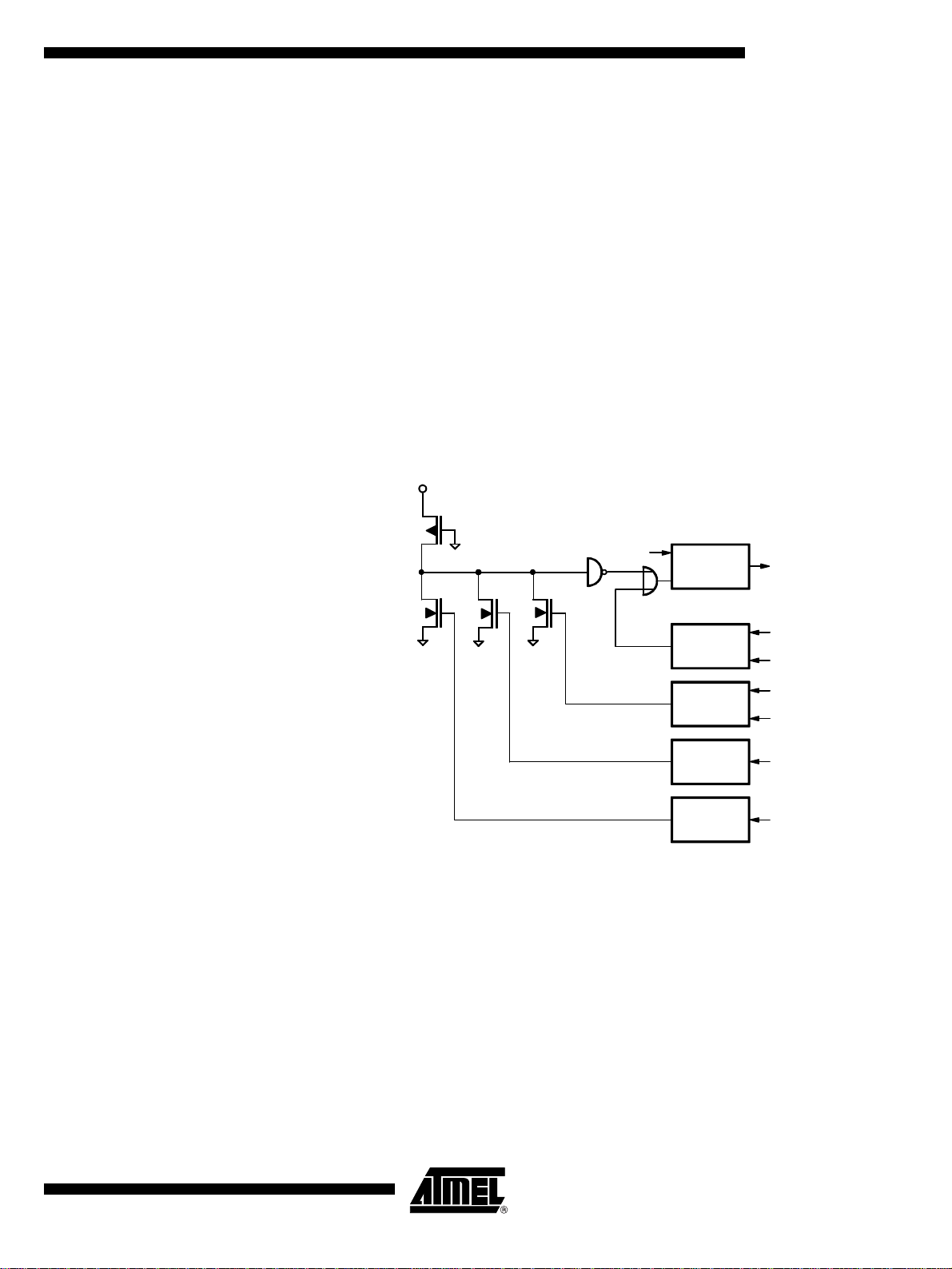
Bi-directional Port 5 As all othe r bi- direct ional ports , this por t in clud es a bitwise pro grammab le Control Reg-
ister (P5CR), which allows the individual programming of each port bit as input or
output. It also opens up the possibility of reading the pin condition when in output mode.
This is a useful feature for self testing and for serial bus applications.
The port pins can also be used as external interrupt inputs (see F igure 23 and Figure
24). The interru pts (INT1 and INT 6) can be ma sked or inde pendent ly co nfigured to trigger on either edge. The interrupt configuration and port direction is controlled by the Port
5 Control Register (P5CR). An additional low resistance pull-up/-down transistor mask
option provides an internal bus pull-up for serial bus applications.
The Port 5 Data Register (P5DAT) is I/O mapped to the primary address r egister of
address "5"h and the Port 5 Control Register (P5CR) to the corresponding auxiliary register. The P5CR is a byte-wide register and is configured by writing first the low nibble
and then the high nibble (see section "Addressing Peripherals").
35
4552B–4BMCU–02/03
Page 36

Figure 30. Bi-directional Port 5
I/O Bus
(Data out)
I/O Bus
Master reset
IN enable
D
P5DATy
S
Q
Mask options
Figure 31. Port 5 External Interrupts
BP52
Data in
Bidir. Port
IN_Enable
I/O-bus
V
DD
*
INT1 INT6
Switched
pull-up
*
*
V
DD
Static
pull-up
*
BP5y
V
*
*
DD
*
Switched
pull-down
I/O-bus
Static
*
Pull-down
Data in
Bidir. Port
IN_Enable
BP51
BP53
Data in
Bidir. Port
IN_Enable
Decoder Decoder Decoder Decoder
P53M2 P53M1 P52M2 P52M1 P51M2 P51M1 P50M2 P50M1
P5CR:
Data in
Bidir. Port
IN_Enable
BP50
Port 5 Data Register (P5DAT) Primary register address: "5"hex
Bit 3Bit 2Bit 1Bit 0
P5DAT3 P5DAT2 P5DAT1 P5DAT0 Reset value: 1111b
Port 5 Control Register (P5CR)
Auxiliary register address: "5"hex
Byte Write
Bit 3Bit 2Bit 1Bit 0
First write cycle P51M2 P51M1 P50M2 P50M1 Reset value: 1111b
Bit 7Bit 6Bit 5Bit 4
Second wr ite cycle P53M2 P53M1 P52M2 P52M1 Re set value: 1111b
36
ATAR862-4
4552B–4BMCU–02/03
Page 37

ATAR862-4
Table 7. P5xM2, P5xM1 – Port 5x Interrupt Mode/Direction Code
Auxiliary Address: "5"hex First Write Cycle Second Write Cycle
Code
3 2 1 0 Function
x x 1 1 BP50 in input mode
x x 0 1 BP50 in input mode
x x 1 0 BP50 in input mode
x x 0 0 BP50 in output mode
1 1 x x BP51 in input mode
0 1 x x BP51 in input mode
1 0 x x BP51 in input mode
0 0 x x BP51 in output mode
– interrupt disabled x x 1 1 BP52 in input mode – interrupt disabled
– rising edge interrupt x x 0 1 BP52 in input mode – rising edge interrupt
– falling edge interrupt x x 1 0 BP52 in input mode – falling edge interrupt
– interrupt disabled x x 0 0 BP52 in output mode – interrupt disabled
– interrupt disabled 1 1 x x BP53 in input mode – interrupt disabled
– rising edge interrupt 0 1 x x BP53 in input mode – rising edge interrupt
– falling edge interrupt 1 0 x x BP53 in input mode – falling edge interrupt
– interrupt disabled 0 0 x x BP53 in output mode – interrupt disabled
Bi-directional Port 4 The bi-directional Port 4 is a bitwise configurable I/O port and provides the external pins
for the Timer 2, SSI and the voltage monitor input (VMI). As a normal port, it performs in
exactly the same way as bi-directional Port 2 (see Figure ). Two additional multiplexes
allow data and port direct ion con trol to be passe d over to othe r intern al modul es (Ti mer
2, VM or SSI). The I/O - pin s f or SC and SD li ne h av e an add iti ona l m ode to g enerate an
SSI-interrupt.
Code
3 2 1 0 Function
All four Port 4 pins can be individually switched by the P4CR-register. Figure shows the
internal interfaces to bi-directional Port 4.
Figure 32. Bi-directional Port 4 and Port 6
I/O Bus
Intx
PIn
POut
I/O Bus
Master reset
I/O Bus
PDir
D
PxDATy
S
S
PxCRy
Q
(Direction)
QD
PxMRy
Mask options
*
*
V
DD
Switched
*
pull-up
*
*
*
Switched
pull-down
V
DD
Static
*
pull-up
BPxy
V
DD
Static
*
pull-down
4552B–4BMCU–02/03
37
Page 38

Port 4 Data Register (P4DAT) Primary register address: "4"hex
Bit 3 Bit 2 Bit 1 Bit 0
P4DAT3 P4DAT2 P4DAT1 P4DAT0 Reset value: 1111b
Port 4 Control Register (P4CR) Byte Write
Auxiliary register address: "4"hex
Bit 3Bit 2Bit 1Bit 0
First write cycle P41M2 P41M1 P40M2 P40M1 Reset value: 1111b
Bit 7Bit 6Bit 5Bit 4
Second wr ite cycle P43M2 P43M1 P42M2 P42M1 Re set value: 1111b
P4xM2, P4xM1 –
Auxiliary Address: "4"hex
Code
3 2 1 0 Function
x x 1 1 BP40 in input mode x x 1 1 BP42 in input mode
x x 1 0 BP40 in output mode x x 1 0 BP42 in output mode
x x 0 1 BP40 enable alternate function
x x 0 0 BP40 enable alternate function
1 1 x x BP41 in input mode 1 0 x x BP43 in output mode
1 0 x x BP41 in output mode 0 1 x x BP43 enable alternate function
0 1 x x BP41 enable alternate function
0 0 x x BP41 enable alternate function
Port 4x Interrupt mode/direction code
First Write Cycle Second Write Cycle
Code
3 2 1 0 Function
x x 0 x BP42 enable alternate function
(SC for SSI)
1 1 x x BP43 in input mode
(falling edge interrupt input for
INT3)
0 0 x x BP43 enable alternate function
(VMI for vol tag e moni tor inp ut)
––
(T2I external clock input fo r
Timer 2)
(T2O for Timer 2)
(SD for SSI)
(falling edge inter rupt input for
INT3)
Bi-directional Port 6 The bi-directional Port 6 is a bitwise configurable I/O port and provides the external pins
for the Timer 3. As a normal port, it performs in exactly the same way as bi-directional
Port 6 (see Figure ). Two additional multiplexes allow data and port direction control to
be passed over to other i ntern al mod ule (T imer 3) . The I/O-pin for T 3I lin e has an add itional mode to generate a Timer 3-interrupt.
All two Port 6 pins can be individually switched by the P6CR register . Figure shows the
internal interfaces to bi-directional Port 6.
38
ATAR862-4
4552B–4BMCU–02/03
Page 39
ATAR862-4
Port 6 Data Register (P6DAT) Primary register address: "6"hex
Bit 3 Bit 2 Bit 1 Bit 0
P6DAT3 – – P6DAT0 Reset value: 1xx1b
Port 6 Control Register (P6CR) Auxiliary register address: "6"hex
Bit 3 Bit 2 Bit 1 Bit 0
P63M2 P63M1 P60M2 P60M0 Reset value: 1111b
Universal Timer/Counter/ Communication Module (UTCM)
P6xM2, P6xM1 –
Code
3 2 1 0 Function
x x 1 1 BP60 in input mode 1 1 x x BP63 in input mode
x x 1 0 BP60 in output mode 1 0 x x BP63 in output mode
x x 0 x
Port 6x Interrupt mode/direction code
Auxiliary Address: "6"hex Write Cycle
BP60 enable alternate port
function (T3O for Timer 3)
Code
3 2 1 0 Function
0 x x x BP63 enable alternate port
function (T3I for Timer 3)
The Universal Timer/counter/Communication Module (UTCM) consi sts of three timers
(Timer 1,Timer 2, Timer 3) and a Synchronous Serial Interface (SSI).
• Timer 1 is an interval timer that can be used to generate periodical interrupts and as
prescaler for Timer 2, Timer 3, the serial interface and the watchdog function.
• Timer 2 is an 8/12-bit timer with an external clock input (T2I) and an output (T2O).
• Timer 3 is an 8-bit timer/counter with its own input (T3I) and output (T3O).
• The SSI operates as two wire serial interface or as shift register for modulation and
demodulation. The modulator and demodulator units work together with the timers
and shift the data bits into or out of the shift register.
4552B–4BMCU–02/03
There is a multitude of modes in whi ch the timers and the serial interface can wo rk
together.
39
Page 40
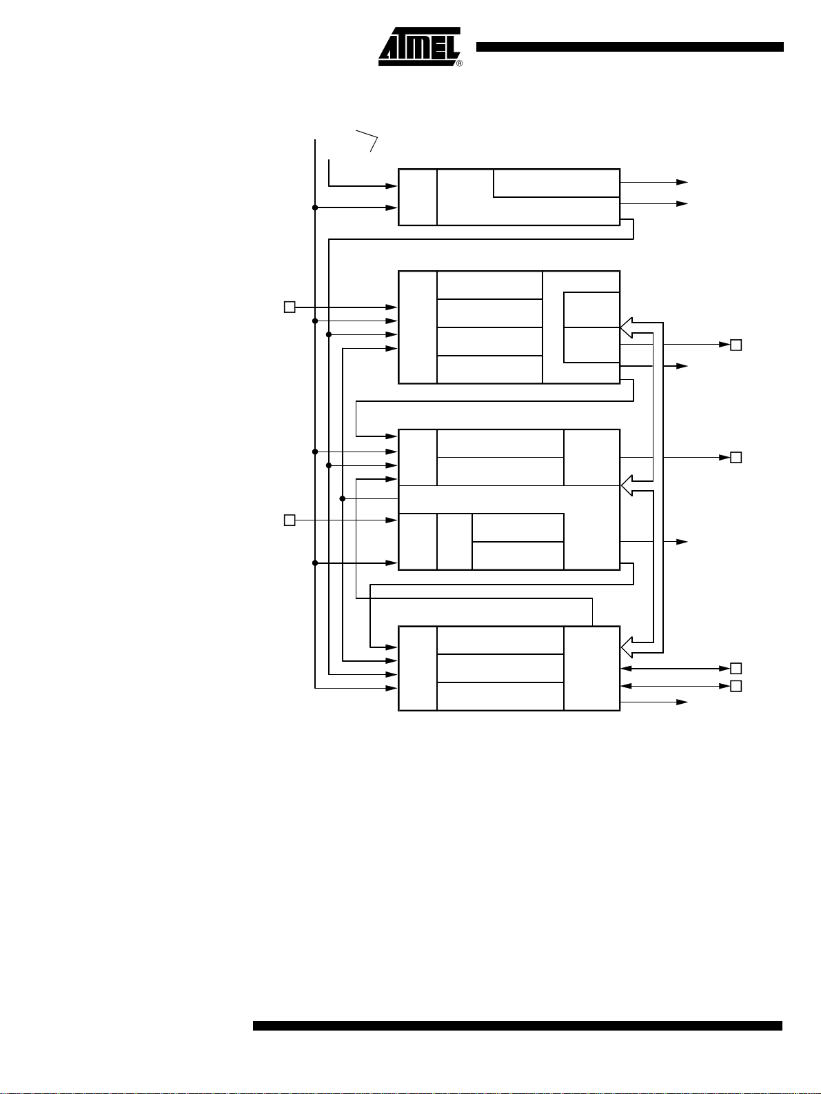
Figure 33. UTCM Block Diagram
T3I
T2I
SYSCL
SUBCL
T1OUT
from clock module
MUX
MUX
TOG3
MUX
POUT
MUX DCG
Timer 1
Interval / Prescaler
Timer 3
Capture 3
8-bit Counter 3
Compare 3/1
Compare 3/2
Timer 2
4-bit Counter 2/1
Compare 2/1
Control
8-bit Counter 2/2
Compare 2/2
Watchdog
Control
Demodu-
lator 3
Modu-
lator 3
Modulator 2
NRST
INT2
T3O
INT5
T2O
I/O bus
INT4
TOG2
MUX
SSI
Receive buffer
8-bit shift register
Transmit buffer
SCL
Control
SC
SD
INT3
Timer 1 The Timer 1 is an interval tim er whic h can be use d to gen er ate pe riod ic al inte rrup ts an d
as prescaler for Timer 2, Timer 3, the serial interface and the watchdog function.
The Timer 1 consists of a programmable 14-stage divider that is driven by either SUBCL
or SYSCL. The timer outp ut s ign al can be u sed as pres ca ler c lock or as SUB CL a nd as
source for the Timer 1 interrupt. Because of other system requirements, the Timer 1 output T1OUT is synchronized with SYSCL. Therefore, in the po wer-down mod e SLEEP
(CPU core -> slee p and OSC-S top -> yes) , the outpu t T1OUT is stopp ed (T1OU T = 0).
Nevertheless, the Timer 1 can be active in SLEEP and generate Timer 1 interrupts. The
interrupt is maskable via the T1IM bit and the SUBCL can be bypassed via the T1BP bit
of the T1C2 register. The time interval for the timer output can be programmed via the
Timer 1 control register T1C1.
40
ATAR862-4
4552B–4BMCU–02/03
Page 41
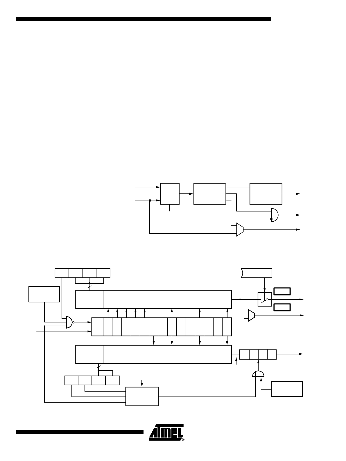
ATAR862-4
This timer starts running automatically after any power-on reset! If the watchdog function is not activated, the timer can be restarted by writing into the T1C1 register with
T1RM = 1.
Timer 1 can also be use d as a watc hdog timer to pr event a syst em from stall ing. The
watchdog timer is a 3-bit counter that is supplied by a separate output of Timer 1. It generates a system reset when the 3-bit counter overflows. To avoid this, the 3-bit counter
must be reset before it ov erflows. The ap plication soft ware has to accom plish this by
reading the CWD register.
After power-on reset t he wa tc hdog mu st be a cti va ted by so ftwar e in the $ RES E T ini tia lization routine. There are two watchdog modes, in one mode the watchdog can be
switched on and off by software, in the other mode the watchdog is active and locked.
This mode can only be stopped by carrying out a system reset.
The watchdog timer operation mode and the time interval for the watchdog reset can be
programmed via the watchdog control register (WDC).
Figure 34. Timer 1 Module
Figure 35. Timer 1 and Watchdog
T1RM T1C2 T1C1 T1C0
T1C1
Write of the
T1C1 register
CL1
3
Decoder
RES
CL
SYSCL
SUBCL
MUX
T1CS
MUX for interval timer
Q5Q1 Q2 Q3 Q4
Q6
Q8
Q8
CL1
Prescaler
14 bit
Q11
Q11
T1MUX
Q14
Q14
WDCL
T1BP
T1C2
T1MUX
SUBCL
Watchdog
4 bit
T1IM
T1BP T1IM
Watchdog
Divider / 8
T1IM=0
T1IM=1
NRST
INT2
T1OUT
INT2
T1OUT
4552B–4BMCU–02/03
Decoder
WDL WDR WDT1 WDT0
WDC
MUX for watchdog timer
2
RES
WDCL
Watchdog
Divider
RESET
CWD register
RESET
(NRST)
Read of the
mode control
41
Page 42

Timer 1 Control Register 1 (T1C1)
Address: "7"hex - Subaddress: "8"hex
Bit 3 * Bit 2 Bit 1 Bit 0
T1RM T1C2 T1C1 T1C0 Reset value: 1111b
* Bit 3 -> MSB, Bit 0 -> LSB
T1RM Timer 1 Restart Mode T1RM = 0, write access without Timer 1 restart
T1RM = 1, write access with Time r 1 restart
Note: If WDL = 0, Timer 1 restart is impossible
T1C2 Timer 1 Control bit 2
T1C1 Timer 1 Control bit 1
T1C0 Timer 1 Control bit 0
The three bits T1C[2:0] select the divider for timer 1. The resulting time interval depends
on this divider and the timer 1 input clock source. The timer input can be supplied by the
system clock, the 32-kHz oscillator or via the clock management. If the clock management generates the SUBCL, the selected input clock fr om the RC oscilla tor, 4-MHz
oscillator or an external clock is divided by 16.
T1C2 T1C1 T1C0 Divider
0 0 0 2 SUBCL/2 61 µs 1 µs/2 µs
0 0 1 4 SUBCL/4 122 µs 2 µs/4 µs
0 1 0 8 SUBCL/8 244 µs 4 µs/8 µs
0 1 1 16 SUBCL/16 488 µs 8 µs/16 µs
1 0 0 32 SUBCL/32 0.977 ms 16 µs/32 µs
1 0 1 256 SUBCL/256 7. 812 ms 128 µs/256 µs
1 1 0 2048 SUBCL/2048 62.5 ms 1024 µs/2048 µs
1 1 1 16384 SUBCL/16384 500 ms 8192 µs/16384 µs
Time Interval with
SUBCL
Time Interval with
SUBCL = 32 kHz
Time Interval with
SYSCL = 2/1 MHz
42
ATAR862-4
4552B–4BMCU–02/03
Page 43
ATAR862-4
Timer 1 Control Register 2 (T1C2)
Watchdog Control Register (WDC)
Address: "7"hex - Subaddress: "9"hex
Bit 3 * Bit 2 Bit 1 Bit 0
– T1BP T1CS T1IM Reset value: x111b
* Bit 3 -> MSB, Bit 0 -> LSB
T1BP Timer 1 SUBCL ByPassed
T1BP = 1, TIOUT = T1MUX
T1BP = 0, T1OUT = SUBCL
T1CS Timer 1 input Clock Select
T1CS = 1, CL1 = SUBCL (see Figure 26)
T1CS = 0, CL1 = SYSCL (see Figure 26)
T1IM Timer 1 Interrupt Mask
T1IM = 1, disables Timer 1 interrupt
T1IM = 0, enables Timer 1 interrupt
Address: "7"hex - Subaddress: "A"hex
Bit 3 * Bit 2 Bit 1 Bit 0
WDL WDR WDT1 WDT0 Reset value: 1111b
* Bit 3 -> MSB, Bit 0 -> LSB
WDL WatchDog Lock mode
WDL = 1, the watchdog can be enabled and disabled by using the WDR-bit
WDL = 0, the watchdog is enabled and locked. In this mode the WDR-bit has no
effect. After the WDL-bit is cleared, the watchdog is active until a
system reset or power-on reset occurs.
WDR WatchDog Run and stop mode
WDR = 1, the watchdog is stopped/disabled
WDR = 0, the watchdog is active/enabled
WDT1 WatchDog Time 1
WDT0 WatchDog Time 0
Both these bits control the time interval for the watchdog reset.
Delay Time to Reset with
WDT1 WDT0 Divider
0 0 512 15.625 ms 0.256 ms/0.512 ms
0 1 2048 62.5 ms 1.024 ms/2.048 ms
1 0 16384 0.5 s 8.2 ms/16.4 ms
1 1 131072 4 s 6 5.5 ms /13 1 ms
SUBCL = 32 kHz
Delay Time to Reset with
SYSCL = 2/1 MHz
4552B–4BMCU–02/03
43
Page 44

Timer 2 8-/12-bit Timer for:
• Interrupt, square-wave, pulse and duty cycle generation
• Baud-rate generation for the internal shift register
• Manchester and Biphase modulation together with the SSI
• Carrier frequency generation and modulation together with the SSI
Timer 2 can be used as an interval timer for inter rupt gen eration, as signal gen erato r or
as baud-rate generator and modulator for the serial interface. It consists of a 4-bit and
an 8-bit up counte r stage whi ch both have compa re regi sters. T he 4-bit c ounter s tages
of Timer 2 are cascadable as a 12-bi t ti mer or as an 8- b it timer wi th 4-bi t pres c ale r. Th e
timer can also be configured as an 8-bit timer and a separate 4-bit prescaler.
The Timer 2 input can be supplied via the system clock, the external input clock (T2I),
the Timer 1 output clock, the Timer 3 outp ut clock or the sh ift clock of the se rial interface. The external input clock T2I is not synchronized with SYSCL. Therefore, it is
possible to use Timer 2 with a higher clock speed than SYSCL. Furthermore, with that
input clock the Timer 2 operates in the power-down mode SLEEP (CPU core -> sleep
and OSC-Stop -> yes) as well as in th e PO WER-DOWN (CPU c ore -> s leep and OSCStop -> no). All other clock sources supplied no clock signal in SLEEP. The 4-bit counter
stages of Timer 2 have an additional clock output (POUT).
Its output has a modulator stage that allows the generation of pulses as well as the generation and modulation of carrier frequencies. The Timer 2 output can modulate with the
shift register data output to generate Biphase- or Manchester code.
If the serial interface is used to modulate a bitstream, the 4-bit stage of Timer 2 has a
special task. The shift register can only handle bitstream lengths divisible by 8. For other
lengths, the 4-bit counter stage can be used to stop the modulator after the right bitcount
is shifted out.
If the timer is used for c arrier f reque ncy mod ulatio n, t he 4-bit stage works togeth er with
an additional 2-bit duty cycle generator like a 6-bit prescaler to generate carrier frequency and duty cycle. The 8-bit counter is used to enable and disable the modulator
output for a programmable count of pulses.
For programming the time interval, the timer has a 4-bit and an 8-bit compare register.
For programming the timer function, it has four mode and control registers. The comparator output of stage 2 is co ntrolled by a speci al compare mode r egister (T2CM) . This
register contains mask bits for the actions (counter reset, output toggle, timer interrupt)
which can be triggered by a compare match event or the counter overflow. This architecture enables the timer function for various modes.
The Timer 2 has a 4-bit compare r egister (T2CO1) and an 8-bit com pare register
(T2CO2). Both these compare registers are cascadable as a 12-bit compare register, or
8-bit compare register and 4-bit compare register.
For 12-bit compare data value: m = x +1 0 £ x £ 4095
For 8-bit compare data value: n = y +1 0 £ y £ 255
For 4-bit compare data value: l = z +1 0 £ z £ 15
44
ATAR862-4
4552B–4BMCU–02/03
Page 45

Figure 36. Timer 2
ATAR862-4
I/O-bus
Timer 2 Modes
Mode 1: 12-bit Compare Counter
T2I
SYSCL
T1OUT
TOG3
SCL
T2C
CL2/1
4-bit Counter 2/1
RES OVF1
Compare 2/1
CM1
T2CO1
POUT
SSI POUT
Control
I/O-bus
T2M1P4CR
CL2/2
DCG
DCGO
8-bit Counter 2/2
RES OVF2
TOG2
Compare 2/2
INT4
T2CO2T2CM
SSI SSI
T2M2
OUTPUT
M2
MOUT
Biphase-,
Manchester-
modulator
SO Control
T2O
to
Modulator 3
Timer 2
modulator
output-stage
The 4-bit stag e and th e 8-bit stage w ork to gethe r as a 12-b it co mpare c ounte r. A com pare match signal of the 4-bit and the 8-bit stage generates the signal for the counter
reset, toggle flip-flop or in terr upt. Th e co mpare action is programmable via the c omp ar e
mode register (T2CM). The 4-bit counter overflow (OVF1) supplies the clock output
(POUT) with clocks. The duty cycle generator (DCG) has to be bypassed in this mode.
Figure 37. 12-bit Compare Counter
Mode 2: 8-bit Compare Counter with 4-bit Programmable Prescaler
RES
DCG
CM1
T2D1, 0
POUT (CL2/1 /16)
8-bit counter
8-bit compare
8-bit register
CL2/1
4-bit count er
4-bit compare
4-bit register
Figure 38. 8-bit Compare Counter
RES
CM1
POUT
DCG
T2D1, 0
8-bit counter
8-bit compare
8-bit register
CL2/1
4-bit counter
4-bit compare
4-bit register
RES
RES
OVF2
CM2
OVF2
CM2
T2RM
T2RM
T2OTM
T2OTM
Timer 2
output mode
and T2OTM-bit
Timer 2
output mode
and T2OTM-bit
TOG2
INT4
T2IM T2CTM
DCGO
TOG2
INT4
T2IM T2CTM
4552B–4BMCU–02/03
45
Page 46

The 4-bit stage is used as programmable pres caler for the 8 -bit counter s tage. In this
mode, a duty cycle stage is also available. This stage can be used as an additional 2-bit
prescaler or for generating duty cycles of 25%, 33% and 50%. The 4-bit compare output
(CM1) supplies the clock output (POUT) with clocks.
Mode 3/4: 8-bit Compare Counter and 4-bit Programmable Prescaler
Figure 39. 4-/8-bit Compare Counter
DCGO
T2I
SYSCL
TOG3
T1OUT
SYSCL
SCL
P41M2, 1P4CR
MUX
T2CS1, 0
CL2/2
CL2/1
DCG
T2D1, 0
8-bit counter
8-bit compare
8-bit register
4-bit counter
4-bit compare
4-bit register
RES
RES
OVF2
CM2
CM1
T2RM
T2OTM
Timer 2
output mode
and T2OTM-bit
TOG2
INT4
T2IM T2CTM
POUT
In these modes the 4-bit and the 8-bit counter stages work independently as a 4-bit
prescaler and an 8- bit tim er wi th a n 2 -b it pr es caler o r as a d uty cyc le gen erato r. O nly i n
the mode 3 and mode 4, can the 8-bit counter be supplied via the external clock input
(T2I) which is selected via the P4CR register. The 4-bit prescaler is started via activating
of mode 3 and stopped and reset in mode 4. Changing mode 3 and 4 has no effect for
the 8-bit timer stage. The 4-bit stage can be used as prescaler for Timer 3, the SSI or to
generate the stop signal for modulator 2 and modulator 3.
Timer 2 Output Modes The signal at the timer output is generated via modulator 2. In the toggle mode, the com-
pare match event toggles the output T2O. For high resolution duty cycle modulation 8
46
bits or 12 bits can be used to toggle the output. In the duty cycle burst
the DCG output is connected to T2O and switched on and off either by the toggle flipflop
output or the serial data line of the SSI. Modulator 2 also has two modes to output the
content of the serial interface as Biphase or Manchester code.
The modulator ou tput stage ca n be configu red by the outp ut control b its in the T2M 2
register. The modulator is started with the start of the s hift register (SIR = 0) and
stopped either by car rying o ut a s hift regi ster stop ( SIR = 1) or c ompar e match event of
stage 1 (CM1) of Timer 2. For this task, Timer 2 mode 3 must be used and the prescaler
has to be supplied with the internal shift clock (SCL).
ATAR862-4
modulator modes
4552B–4BMCU–02/03
Page 47

Figure 40. Timer 2 Modulator Output Stage
DCGO
SO
TOG2
ATAR862-4
T2O
S3
Modulator3
SSI
CONTROL
RE
FE
OMSK
Biphase/
Manchester
modulator
S1
Toggle
RES/SET
T2TOPT2OS2, 1, 0T2M2
M2
S2
M2
Timer 2 Output Signals
Timer 2 Output Mode 1 Toggle Mode A: A Timer 2 compare match toggles the output flip-flop (M2) -> T2O
Figure 41. Interrupt Timer/Square Wave Generator – the Output Toggles with Each
Edge Compare Match Event
Input
Counter 2
T2R
Counter 2
CMx
4000123 40123 40123 01
INT4
T2O
Toggle Mode B: A Timer 2 compare match toggles the output flip-flop (M2) -> T2O
Figure 42. Pulse Generator – the Timer Outp ut Toggles with th e Timer Start if the
T2TS-bit Is Set
Input
Counter 2
T2R
Counter 2
CMx
INT4
T2O
T2O
Toggle
by start
4000123 567 40123 56
4095/
255
4552B–4BMCU–02/03
47
Page 48
Toggle Mode C: A Timer 2 compare match toggles the output flip-flop (M2) -> T2O
Figure 43. Pulse Generator – the Timer Toggles with Timer Overflow and Compare
Match
Input
Counter 2
T2R
Counter 2
CMx
OVF2
INT4
T2O
4000123 567 40123 56
4095/
255
Timer 2 Output Mode 2 Duty Cycle Burst Generator 1: The DCG output signal (DCGO) is given to the output,
and gated by the output flip-flop (M2)
Figure 44. Carrier Frequency Burst Modulation with Timer 2 Toggle Flip-flop Output
DCGO
Counter 2
TOG2
M2
1 2012012345012012345678012345678910012345
T2O
Counter = compare register (=2)
Timer 2 Output Mode 3 Duty Cycle Burst Generator 2: The DCG output signal (DCGO) is given to the output,
and gated by the SSI internal data output (SO)
Figure 45. Carrier Frequency Burst Modulation with the SSI Data Output
DCGO
1 201201201201201201201201201201201201201
Counter = compare register (=2)
Bit 0 Bit 1 Bit 2 Bit 3 Bit 4 Bit 5 Bit 6 Bit 7 Bit 8 Bit 9 Bit 10 Bit 11 Bit 12 Bit 13
4552B–4BMCU–02/03
48
Counter 2
TOG2
SO
T2O
ATAR862-4
Page 49

ATAR862-4
Timer 2 Output Mode 4 Biphase Modulator: Timer 2 Modulates the SSI Internal Data Output (SO) to Biphase
Code.
Figure 46. Biphase Modulation
TOG2
SC
SO
T2O
00110101
Bit 7 Bit 0
0000
Data: 00110101
11 1 1
8-bit SR-Data
Timer 2 Output Mode 5 Manchester Modulator: Timer 2 Modulates t he SSI interna l data output (SO) to
Manchester code
Figure 47. Manchester Modulation
TOG2
SC
SO
T2O
00110101
Bit 7 Bit 0
0
Bit 7 Bit 0
Data: 00110101
11 1 1
8-bit SR-Data
000
Timer 2 Output Mode 7 In t his mo de the timer overfl ow defi nes the per iod and th e comp are regi ster defines th e
duty cycle. During one period only the first comp are ma tch occurrence is used to to ggl e
the timer output flip-flop, until the overflow all further compare match are ignored. This
avoids the situation that changing the compare register causes the occurrence of several compare match during one period. The resolution at the pulse-width modulation
Timer 2 mode 1 is 12-bit and all other Timer 2 modes are 8-bit.
49
4552B–4BMCU–02/03
Page 50

PWM Mode: Pulse-width modulation output on Timer 2 output pin (T2O)
Figure 48. PWM Modulation
Input clock
Counter 2/2
T2R
Counter 2/2
CM2
0 0 50 255 1000 255 0 150 255 0 50 255 0 100
OVF2
INT4
T2O
load the next
compare value
T1 T2 T3 T1 T2
TTT T
T2CO2=150 load load
T
Timer 2 Registers Timer 2 has 6 co ntrol regist ers t o confi gure t he time r mode , the tim e inte rval, the in put
clock and its output function. All registers are indirectly addressed using extended
addressing as descr ibed in s ection "Addr essin g Periph erals ". The a lternate fu nctio ns of
the Ports BP41 or BP42 must be selected with the Port 4 control register P4CR, if one of
the Timer 2 modes require an input at T2I/BP41 or an output at T2O/BP42.
Timer 2 Control Register (T2C) Address: "7"hex - Subaddress: "0"hex
Bit 3Bit 2Bit 1Bit 0
T2CS1 T2CS0 T2TS T2R Reset value: 0000b
T2CS1 Timer 2 Clock Select bit 1
T2CS0 Timer 2 Clock Select bit 0
50
T2CS1 T2CS0 Input Clock (CL 2/1) of Counter Stage 2/1
0 0 Sy stem clock (SYSCL)
0 1 Output signal of Timer 1 (T1OUT)
1 0 Internal shift clock of SSI (SCL)
1 1 Output signal of Timer 3 (TOG3)
T2TS Timer 2 Togg le with Start
T2TS = 0, the output flip-flop of Timer 2 is not toggled with the timer start
T2TS = 1, the output flip-flop of Timer 2 is toggled when the timer is started with
T2R
T2R Timer 2 Run
T2R = 0, Timer 2 stop and reset
T2R = 1, Timer 2 run
ATAR862-4
4552B–4BMCU–02/03
Page 51

ATAR862-4
Timer 2 Mode Register 1 (T2M1)
Address: "7"hex - Subaddress: "1"hex
Bit 3Bit 2Bit 1Bit 0
T2D1 T2D0 T2MS1 T2MS0 Reset value: 1111b
T2D1 Timer 2 Duty cycle bit 1
T2D0 Timer 2 Duty cycle bit 0
Function of Duty Cycle Generator
T2D1 T2D0
1 1 Bypassed (DCGO0) /1
1 0 Duty cycle 1/1 (DCGO1) /2
0 1 Duty cycle 1/2 (DCGO2) /3
0 0 Duty cycle 1/3 (DCGO3) /4
T2MS1 Timer 2 Mode Select bit 1
T2MS0 Timer 2 Mode Select bit 0
(DCG) Additional Divider Effect
Mode T2MS1 T2MS0 Clock Output (POUT) Timer 2 Modes
1 1 1 4-bit counter overflow (OVF1) 12-bit compare counter; the
DCG has to be bypassed in
this mode
2 1 0 4-bit compare output (CM1) 8-bit compar e counter with 4-
bit programmable prescaler
and duty cycle generator
3 0 1 4-bit compare output (CM1) 8-bit compare counter clocked
by SYSCL or the external clock
input T2I, 4-bit prescaler run,
the counter 2/1 starts after
writing mode 3
4 0 0 4-bit compare output (CM1) 8-bit compare counter clocked
by SYSCL or the external clock
input T2I, 4-bit prescaler stop
and resets
Duty Cycle Generator The duty cycle generator generat es duty c ycles o f 25%, 33% o r 50%. The frequ ency at
the duty cycle generator output depends on the duty cycle and the Timer 2 prescaler
setting. The DCG-stage can also be used as additional programmable prescaler for
Timer 2.
4552B–4BMCU–02/03
51
Page 52
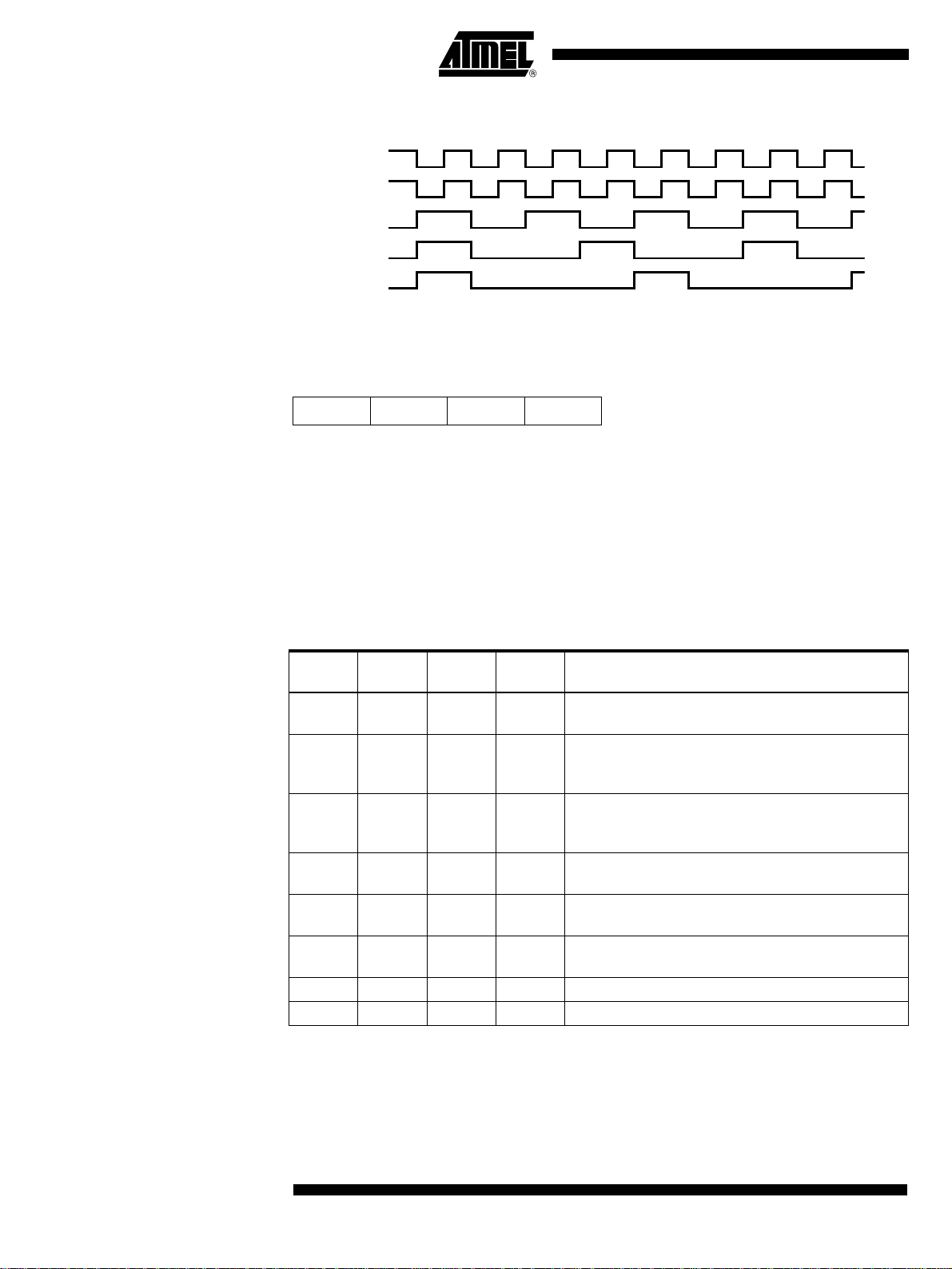
Figure 49. DCG Output Signals
DCGIN
DCGO0
DCGO1
DCGO2
DCGO3
Timer 2 Mode Register 2 (T2M2)
Address: "7"hex - Subaddress: "2"hex
Bit 3Bit 2Bit 1Bit 0
T2TOP T2OS2 T2OS1 T2OS0 Reset value: 1111b
T2TOP Timer 2 Toggle Output Preset
This bit allows the programmer to preset the Timer 2 output T2O.
T2TOP = 0, resets the toggle outputs with the write cycle (M2 = 0)
T2TOP = 1, sets toggle outputs with the write cycle (M2 = 1)
Note: If T2R = 1, no output preset is possible
T2OS2 Timer 2 Output Select bit 2
T2OS1 Timer 2 Output Select bit 1
T2OS0 Timer 2 Output Select bit 0
Output
Mode T2OS2 T2OS1 T2OS0 Clock Output (POUT)
1111Toggle mode: a Timer 2 compare match toggles
the output flip-flop (M2) -> T2O
2110Duty cycle burst generator 1: the DCG output
signal (DCG0) is given to the output and gated by
the output flip-flop (M2)
3101Duty cycle burst generator 2: the DCG output
signal (DCGO) is given to the output and gated by
the SSI internal data output (SO)
4100Biphase modulator: Timer 2 modulates the SSI
internal data output (SO) to Biphase code
5011Manchester modulator: Timer 2 modulates the SSI
internal data output (SO) to Manchester code
6010SSI output: T2O is used directly as SSI internal
data output (SO)
7001PWM mode: an 8/12-bit PWM mode
8000Not allowed
52
If one of these output modes is used the T2O alternate function of Port 4 must also be
activated.
ATAR862-4
4552B–4BMCU–02/03
Page 53

ATAR862-4
Timer 2 Compare and Compare Mode Registers
Timer 2 Compare Mode Register (T2CM)
Timer 2 has two s eparate com pare r egister s, T2 CO1 for the 4-bit stage and T2CO2 for
the 8-bit stage of Timer 2. The timer compares the contents of the compare register current counter value and if it matches it generates an output signal. Dependent on the
timer mode, this signal is used to generate a timer interrupt, to toggle the output flip-flop
as SSI clock or as a clock for the next counter stage.
In the 12-bit timer mode, T2CO1 contains bits 0 to 3 and T2CO2 bits 4 to 11 of the 12-bit
compare value. In all other modes, the two compare registers work independently as a
4- and 8-bit compare register.
When asigned to the compare register a compare event will be suppressed.
Address: "7"hex - Subaddress: "3"hex
Bit 3Bit 2Bit 1Bit 0
T2OTM T2CTM T2RM T2IM Reset value: 0000b
T2OTM Timer 2 Overflow Toggle Mask bit
T2OTM = 0, disable overflow toggle
T2OTM = 1, enable overflow toggle, a counter overflow (OVF2) toggles output
flip-flop (TOG2). If the T2OTM-bit is set, only a counter overflow can
generate an interrupt except on the Timer 2 output mode 7.
T2CTM Timer 2 Compare Toggle Mask bit
T2CTM = 0, disable compare toggle
T2CTM = 1, enable compare toggle, a match of the counter with the compare
register toggles output flip-flop (TOG2). In Timer 2 output mode 7 and
when the T2CTM-bit is set, only a match of the counter with the
compare register can generate an interrupt.
Timer 2 COmpare Register 1 (T2CO1)
T2RM Timer 2 Reset Mask bit
T2RM = 0, disable counter reset
T2RM = 1, enable counter reset, a match of the counter with the compare register
resets the counter
T2IM Timer 2 Interrupt Mask bit
T2IM = 0, disable Timer 2 interrupt
T2IM = 1, enable Timer 2 interrupt
Timer 2 Output Mode T2OTM T2CTM Timer 2 Interrupt Source
1, 2, 3, 4, 5 and 6 0 x Compare match (CM2)
1, 2, 3, 4, 5 and 6 1 x Overflow (OVF2)
7 x 1 Compare match (CM2)
Address: "7"hex - Subaddress: "4"hex
Write cycle Bit 3 Bit 2 Bit 1 Bit 0 Reset value: 1111b
In prescaler mode the clock is bypassed if the compare register T2CO1 contains 0.
4552B–4BMCU–02/03
53
Page 54

Timer 2 COmpare Register 2 (T2CO2) Byte Write
First write cycle Bit 3 Bit 2 Bit 1 Bit 0 Reset value: 1111b
Second write cycle Bit 7 Bit 6 Bit 5 Bit 4 Reset value: 1111b
Timer 3
Features • Two Compa re Reg iste rs
• Capture Register
• Edge Sensitive Input with Zero Cross Detection Capability
• Trigger and Single Action Modes
• Output Control Modes
• Automatically Modulation and Demodulation Modes
• FSK Modulation
• Pulse Width Modulation (PWM)
• Manchester Demodulation Together with SSI
• Biphase Demodulation Together with SSI
• Pulse-width Demodulation Together with SSI
Address: "7"hex - Subaddress: "5"hex
Figure 50. Timer 3
Capture register
CL3
8-bit counter
8-bit comparator
Compare register 1
Compare register 2
TOG2 T3I
Control
RES
Control
C31
C32
NQ
NQ
T3EIM
INT5
D
T3SM1
CM31
CM32
D
T3RM1 T3IM1 T3TM1
T3TM2T3IM2T3RM2T3SM2
: T3M1
TOG3
: T3M2
54
ATAR862-4
4552B–4BMCU–02/03
Page 55

ATAR862-4
Timer 3 consists of an 8-bit up-counter with two compare registers and one capture register. The timer can be used as event counter, timer and signal generator. Its output can
be programmed as modulator and d emodulator for the s erial i nterface. The two compare registers enable various modes of signal generation, modulation and
demodulation. The counter can be driven by internal and external clock sources. For
external clock sources, it has a programmable edge-sensitive input which can be used
as counter input, capture signal input or trigger input. This timer input is synchronized
with SYSCL. Therefore, in the power-down mode SLEEP (CPU core -> sleep and OSCStop -> yes), this ti mer i npu t is s topp ed t oo. T h e coun ter is read abl e v ia its captu r e r egister while it is running. In capture mode, the cou nter value can be captured by a
programmable capture event from the Timer 3 input or Timer 2 output.
A special feature of this timer is the trigger- and single-action mode. In trigger mode, the
counter starts counting triggered by the external signal at its input. In single-action
mode, the counter counts only one time up to the programmed compare match event.
These modes are very usef ul for modulat ion, demodula tion, signal gene ration, signa l
measurement and phase controlling. For phase controlling, the timer input is protected
against negative voltages and has zero-cross detection capability.
Timer 3 has a modulator output stage and input functions for demodulation. As modulator it works together wi th Timer 2 or the serial int erface. W hen the sh ift regist er is used
for modulation the data shifted out of the register is encoded bitwise. In all demodulation
modes, the decoded data bits are shifted automatically into the shift register.
Timer/Counter Modes Timer 3 has 6 timer modes and 6 modulator/demodulator modes. The mode is set via
the Timer 3 Mode Register T3M.
In all these modes, the co mpa re r egi st er and the compare-mode register bel ong ing to i t
define the counter value for a compare match and the action of a compare match. A
match of the current counter value with the content of one compare register triggers a
counter reset, a Timer 3 interrupt or the toggling of the output flip-flop. The compare
mode registers T3M1 an d T3M2 cont ain the mask bi ts for enabl ing or disabl ing these
actions.
The counter can al so be e nabled to execut e single a ctions with one or both compare
registers. If thi s mo de i s set t he cor resp ondin g c ompar e m atch ev ent i s g enerate d on ly
once after the counter start.
Most of the timer modes use their compare registers alternately. After the start has been
activated, the first comparison is carried out via th e compare register 1, the second is
carried out via the compare register 2, the third is carried out again via the compare register 1 and so on. This makes it easy to generate signals with cons tant periods and
variable duty cycle or to generate signals with variable pulse and space widths.
If single-action mode is set for one compare register, the comparison is always carried
out after the first cycle via the other compare register.
The counter can be st arted an d stoppe d via the con trol reg ister T3C. T his regis ter also
controls the initia l level of the output bef ore start. T 3C contains th e interrupt mask for a
T3I input interrupt.
Via the Timer 3 clock-s elect register, the i nternal or external cloc k source can be
selected. This regi ster sele ct s also th e active edge of the exter nal inp ut. An edge at the
external input T 3I c an ge nerat e also an i nterrup t if the T 3EIM -bit is se t and the T imer 3
is stopped (T3R = 0) in the T3C-register.
4552B–4BMCU–02/03
55
Page 56

Figure 51. Counter 3 Stage
CL3
Compare register 1
Compare register 2
Capture register
8-bit counter
8-bit comparator
TOG2 T3I
Control
RES
Control
C31
C32
NQ
NQ
D
T3SM1
CM31
CM32
D
T3EIM
T3RM1 T3IM1 T3TM1
T3TM2T3IM2T3RM2T3SM2
INT5
: T3M1
TOG3
: T3M2
The status of the timer as well as the occurrence of a compare match or an edge detect
of the input signal is indicated by the status register T2ST. This allows identification of
the interrupt source because all these events share only one timer interrupt.
Timer 3 – Mode 1: Timer/Counter
Timer 3 compares data values.
The Timer 3 has two 8-bit compare registers (T3CO1, T3CO2). The compare data value
can be ‘m’ for each of the Timer 3 compare registers.
The compare data value for the compare registers is: m = x +1 0 £ x £ 255
The selected clock from an internal or external source increments the 8-bit counter. In
this mode, the timer ca n be use d as ev ent co unter for external clock s at T3I or as timer
for generating interrupts and puls es at T3O . The co unter val ue can be read by th e software via the capture register.
56
ATAR862-4
4552B–4BMCU–02/03
Page 57

ATAR862-4
Figure 52. Counter Reset with Each Compare Match
T3R
Counter 3
CM31
CM32
INT5
T3O
Figure 53. Counter Reset with Compare Register 2 and Toggle with Start
CL3
T3R
Counter 3
0000123 51234 00123 12
4000123 567 40123 56
89
3
CM31
CM32
INT5
T3O
Toggle
T3O
by start
Figure 54. Single Action of Compare Register 1
T3R
Counter 3
CM31
CM32
T3O
0 012345678910012
Toggle by start
01201201201201201201201201
Timer 3 – Mode 2: Timer/Counter, External Trigger Restart and External Capture (with T3I Input)
4552B–4BMCU–02/03
The counter is driven b y an internal cl ock source. After starti ng with T3R, the fir st edge
from the external input T3I starts the counter. The following edges at T3I load the current counter value into the ca pture register, res et the counter and r estart it. The ed ge
can be selected by the programmable edge decoder of the timer input stage. If singleaction mode is activated for one or both compare registers the trigger signal restarts the
single action.
57
Page 58

Figure 55. Externally Trigge red Cou nter Res et and S tart Com bined wi th Sing le-act ion
Mode
T3R
Counter 3
T3EX
CM31
CM32
T3O
00000000123456
78910012XXX012345678910012XX
XX
Timer 3 – Mode 3: Timer/Counter, Internal Trigger Restart and Internal Capture (with TOG2)
Timer 3 – Mode 4: Timer/Counter
Timer 3 – Mode 5: Timer/Counter, External Trigger Restart and External Capture (with T3I Input)
The counter is driven by an internal or external (T3I) clock source. The output toggle signal of Timer 2 resets the counter. The counter value before the reset is saved in the
capture register. If single-action mode is activated for one or both compare registers, the
trigger signal restarts the single actions. This mode can be used for frequency measurements or as event counter with time gate (see combination mode 10).
Figure 56. Event Counter with Time Gate
T3R
T3I
Counter 3
TOG2
T3CP-
Register
0012345678910
Capture value = 0 Capture value = 11
11 0 1 2 401
3
2
Capture
value = 4
The timer runs as timer/counter in mode 1, but its output T3O is used as output for the
Timer 2 output signal.
The Timer 3 runs as timer/counter in mode 2, but its output T3O is used as output for the
Timer 2 output signal.
Timer 3 Modulator/Demodulator Modes
Timer 3 – Mode 6:
Carrier Frequency Burst
Modulation Controlled by
Timer 2 Output T oggle FlipFlop (M2)
58
ATAR862-4
The Timer 3 counter is drive n by an inte rnal or ex ternal cl ock sour ce. Its comp are- an d
compare mode registers must be programmed to generate the car rier freque ncy vi a the
output toggle flip-flop. The out put toggle flip-fl op of Timer 2 is used to enable or disable
the Timer 3 output. Time r 2 can be driven by the toggl e output signa l of Timer 3 or any
other clock source (see combination mode 11).
4552B–4BMCU–02/03
Page 59
ATAR862-4
Timer 3 – Mode 7: Carrier Frequency Burst Modulation Controlled by SSI Internal Output (SO)
Timer 3 – Mode 8: FSK Modulation with Shift Register D ata (SO)
The Timer 3 counter is drive n by an inte rnal or ex ternal cl ock sour ce. Its comp are- an d
compare mode registers must be programmed to generate the car rier freque ncy vi a the
output toggle flip-flop. T he ou tput (SO ) of the S SI is us ed to en abl e or disabl e the Timer
3 output. The SSI should be supplied with the toggle signal of Timer 2 (see combination
mode 12).
The two compare registers are used for generating two di fferent time intervals . The SSI
internal data out put (SO) sel ects which compare r egister is u sed for the output frequency generation. A "0" level at the SSI data outpu t ena ble s t he c om par e register 1. A
"1" level enables compare register 2. The compare- and compare-mode registers must
be programmed t o gen erate the two fr eque ncie s vi a th e outp ut tog gle flip-fl op. T he SSI
can be supplied with the toggle signal of Timer 2. The Timer 3 counter is driven by an
internal or external clock source. The Timer 2 counter is driven by the Counter 3 (TOG3)
(see also combination mode 13).
Figure 57. FSK Modulation
T3R
Counter 3
CM31
CM32
01234012340123
40120120120120120120120123
40
1
Timer 3 – Mode 9: Pulse-width Modulation with the Shift Regis ter
SO
T3O
01 0
The two compare registers are used for generating two di fferent time intervals . The SSI
internal data output (SO) selects which compare register is used for the output pulse
generation. In this mode both compare- an d compare-m ode regist ers must be pr ogrammed for generating the two pulse widths. It is also useful to enable the single-action
mode for extreme duty cycles. Timer 2 is used as baudrate generator and for the trigger
restart of Timer 3. The SSI must be supplied with a toggle signal of Timer 2. The counter
is driven by an internal or external clock source (see combination mode 7).
Figure 58. Pulse-width Modulation
TOG2
SIR
SO
SCO
T3R
Counter 3
CM31
000000000 0000
00000123456789101112131415012345
00 1
67819111210 1413 0 2 314150
4552B–4BMCU–02/03
CM32
T3O
59
Page 60

Timer 3 – Mode 10: Manchester Demodulation/ Pulse-width Demodulation
For Manchester demodula tion , the edge detec ti on sta ge mus t be progr am me d to detec t
each edge at the input. These edges are evaluated by the demodulator stage. The timer
stage is used to generate the shift clock for the SSI. The com pare register 1 match
event defines the correct moment for shifting the state from the input T3I as the decoded
bit into shift register – after that the demo dulator waits for the ne xt edge to synchr onize
the timer by a reset for the next bit. The compare register 2 can also be used to detect a
time-out error and handle it with an interrupt routine (see also combination mode 8).
Figure 59. Manchester Demodulation
Timer 3 – Mode 11: Biphase Demodulation
Timer 3
mode
T3I
T3EX
SI
CM31=SCI
SR-DATA
Synchronize Manchester demodulation mode
1011100110
11
BIT 0 BIT 1 BIT 2 BIT 3 BIT 4
100110
BIT 5
BIT 6
In the Biphase demodulation mode, the timer operates like in Manchester demodulation
mode. The difference is that the bits are decoded via a toggle flip-flop. This flip-flop samples the edge in the middle of the bitframe and the compare register 1 match ev ent
shifts the toggle flip-flop output into shift register (see also combined mode 9).
Figure 60. Biphase Demodulation
Timer 3
mode
T3I
Synchronize Biphase demodulation mode
011 1 1
0000
60
ATAR862-4
T3EX
Q1=SI
CM31=SCI
Reset
Counter 3
SR-DATA
01
BIT 0 BIT 1 BIT 2 BIT 3 BIT 4 BIT 5 BIT 6
101010
4552B–4BMCU–02/03
Page 61

ATAR862-4
Timer 3 – Mode 12: Timer/Counter with External Capture Mode (T3I)
Timer 3 Modulator for Carrier Frequency Burst Modulation
The counter is driven by an internal clock source and an edge at the external input T3I
loads the counter value into the capture register. The edge can be selected with the programmable edge detector of the timer input stage. This mode can be used for signal and
pulse measurements.
Figure 61. External Captur e Mode
T3R
T3I
Counter 3
T3CP-
Register
01234567891011
0 121314 16 20171819 2221 23 27242526 2928 30 34313233 3635 37 41383940
Capture value = X
15
Capture value = 17
Capture
value = 35
If the output stage operates as puls e-width modulato r for the sh ift register , the output
can be stopped with stage 1 of T imer 2. For this task, the timer mode 3 must be used
and the prescaler must be supplied by the internal shift clock of the shift register.
The modulator can be started with the start of the shift register (SIR = 0) and stopped
either by a shift register stop (SIR = 1) or compare match event of stage 1 of Timer 2.
For this task, the Timer 2 must be used in mode 3 and the prescaler stage must be supplied by the internal shift clock of the shift register.
Figure 62. Modulator 3
Timer 3 Demodulator for Biphase, Manchester and Pulse-width-modulated Signals
0
T3
TOG3
SO
M2
SSI/
Control
Set
T3TOP
Res
M3
OMSK
1
2
MUX
3
T3M
T3O
Timer 3 Mode T3O
6 MUX 1
7 MUX 2
9 MUX 3
other MUX 0
The demodulator stage of Timer 3 can be used to decode Biphase, Manchester and
pulse-width-coded signals.
Figure 63. Timer 3 Demodulator 3
T3M
T3I
T3EX
Demodulator 3
CM31
Counter 3
Counter 3
Control
Res
Reset
SCI
SI
4552B–4BMCU–02/03
61
Page 62

Timer 3 Registers
Timer 3 Mode Register (T3M) Address: "B"hex - Subaddress: "0"hex
Bit 3Bit 2Bit 1Bit 0
T3M3 T3M2 T3M1 T3M0 Reset value: 1111b
T3M3 Timer 3 Mode select bit 3
T3M2 Timer 3 Mode select bit 2
T3M1 Timer 3 Mode select bit 1
T3M0 Timer 3 Mode select bit 0
Mode T3M3 T3M2 T3M1 T3M0 Timer 3 Modes
11111Timer/counter with a read access
21110Timer/counter, external capture and external
trigger restart mode (T3I)
31101Timer/counter, internal capture and internal
trigger restart mode (TOG2)
41100Timer/counter mode 1 without output (T2O ->
T3O)
51011Timer/counter mode 2 without output (T2O ->
T3O)
61010Burst modulation with Timer 2 (M2)
71001Burst modulation with shift register (SO)
81000FSK modulation with shift register (SO)
90111Pulse-width modulation with shift register (SO)
and Timer 2 (TOG2), internal trigger restart
(SCO) -> counter reset
100110Manchester demodulation/pulse-width
demodulation
110101Biphase demodulation (T2O -> T3O)
120100Timer/counter with external capture mode (T3I)
130011Not allowed
140010Not allowed
150001Not allowed
160000Not allowed
Note: 1. In this mode, the SSI can be used only as demodulator (8-bit NRZ rising edge). All
other SSI modes are not allowed.
(1)
(T2O -> T3O)
62
ATAR862-4
4552B–4BMCU–02/03
Page 63

ATAR862-4
Timer 3 Control Register 1 (T3C) Write
Timer 3 Status Register 1 (T3ST) Read
Primary register address: "C"hex - Write
Bit 3 Bit 2 Bit 1 Bit 0
Write T3EIM T3TOP T3TS T3R Reset value: 0000b
T3EIM Timer 3 Edge Interrupt Mask
T3EIM = 0, disables the interrupt when an edge event for Timer 3 occurs (T3I)
T3EIM = 1, enables the interrupt when an edge event for Timer 3 occurs (T3I)
T3TOP Timer 3 Toggle Output Preset T3TOP = 0, sets toggle output (M3) to "0"
T3TOP = 1, sets toggle output (M3) to "1"
Note: If T3R = 1, no output preset is possible
T3TS Timer 3 Toggle with Start T3TS = 0, Timer 3 output is not toggled during the start
T3TS = 1, Timer 3 output is toggled if started with T3R
T3R Timer 3 Run T3R = 0, Timer 3 stop and reset
T3R = 1, Timer 3 run
Primary register address: "C"hex - Read
Bit 3 Bit 2 Bit 1 Bit 0
Timer 3 Clock Select Register (T3CS)
Read - - - T3ED T3C2 T3C1 Reset value: x000b
T3ED Timer 3 Edge Detect
This bit will be set by the edge-detect logic of Timer 3 input (T3I)
T3C2 Timer 3 Compare 2
This bit will be set when a match occurs between Counter 3 and T3CO2
T3C1 Timer 3 Compare 1
This bit will be set when a match occurs between Counter 3 and T3CO1
Note: The status bits T3C1, T3C2 and T3ED will be reset after a READ access to T3ST.
Address: "B"hex - Subaddress: "1"hex
Bit 3 Bit 2 Bit 1 Bit 0
T3CS T3E1 T3E0 T3CS1 T3CS0 Reset value: 1111b
T3E1 Timer 3 Edge select bit 1 T3E1 T3E0 Timer 3 Input Edge Select (T3I)
T3E0 Timer 3 Edge select bit 0 11–
1 0 Positive edge at T3I pin
0 1 Negative edge at T3I pin
4552B–4BMCU–02/03
0 0 Each edge at T3I pin
63
Page 64

T3CS1 Timer 3 Clock Source select bi t 1 T3CS1 TCS0 Counter 3 Input Signal (CL3)
T3CS0 Timer 3 Clock Source select bi t 0 1 1 System clock (SYSCL)
1 0 Output signal of Timer 2 (POUT)
0 1 Output signal of Timer 1 (T1OUT)
0 0 External input signal from T3I edge
detect
Timer 3 Compare- and Compare-mode Register
Timer 3 Compare-Mode Register 1 (T3CM1)
Timer 3 has two separate compare registers T3CO1 and T3CO2 for the 8-bit stage of
Timer 3. The timer compares the content of the comp are register with the current
counter value. If both match, it generates a signal. This signal can be used for the
counter reset, to gene ra te a ti me r interrupt, for toggling the outp ut flip-flop, as SSI clock
or as clock for the next counter stage. For each compare register, a compare-mode register exists. These registe rs contain mas k bits to enable or disabl e the generati on of an
interrupt, a counter reset, or an output toggling with the occurrence of a compare match
of the corresponding compare register. The mask bits for activating the single-action
mode can also be located in the compare mode registers. When assigned to the compare register a compare event will be suppressed.
Address: "B"hex - Subaddress: "2"hex
Bit 3Bit 2Bit 1Bit 0
T3CM1 T3SM1 T3TM1 T3RM1 T3IM1 Reset value: 0000b
T3SM1 Timer 3 Single action Mask bit 1
T3SM1 = 0, disables single-action compare mode
T3SM1 = 1, enables single-compare mode. After this bit is set, the compare
register (T3CO1) is used until the next compare match.
T3TM1 Timer 3 compare Toggle action Mask bit 1
T3TM1 = 0, disables compare toggle
T3TM1 = 1, enables compare toggle. A match of Counter 3 with the compare
register (T3CO1) toggles the output flip-flop (TOG3).
T3RM1 Timer 3 Reset Mask bit 1
T3RM1 = 0, disables counter reset
T3RM1 = 1, enables counter reset. A match of Counter 3 with the compare
register (T3CO1) resets the Counter 3.
64
T3IM1 Timer 3 Interrupt Mas k bit 1
T3RM1 = 0, disables Timer 3 inte rrupt for T3CO1 register.
T3RM1 = 1, enables Timer 3 interrupt for T3CO1 register.
T3CM1 contains the mask bits for the match event of the Counter 3 compare re gister 1
ATAR862-4
4552B–4BMCU–02/03
Page 65

ATAR862-4
Timer 3 Compare Mode Register 2 (T3CM2)
Address: "B"hex - Subaddress: "3"hex
Bit 3Bit 2Bit 1Bit 0
T3CM2 T3SM2 T3TM2 T3RM2 T3IM2 Reset value: 0000b
T3SM2 Timer 3 Single action Mask bit 2
T3SM2 = 0, disables single-action compare mode
T3SM2 = 1, enables single-compare mode. After this bit is set, the compare
register (T3CO2) is used until the next compare match.
T3TM2 Timer 3 compare Toggle action Mask bit 2
T3TM2 = 0, disables compare toggle
T3TM2 = 1, enables compare toggle. A match of Counter 3 with the compare
register (T3CO2) toggles the output flip-flop (TOG3).
T3RM2 Timer 3 Reset Mask bit 2
T3RM2 = 0, disables counter reset
T3RM2 = 1, enables counter reset. A match of Counter 3 with the compare
register (T3CO2) resets the Counter 3.
T3IM2 Timer 3 Interrupt Mas k bit 2
T3RM2 = 0, disables Timer 3 inte rrupt for T3CO2 register.
T3RM2 = 1, enables Timer 3 interrupt for T3CO2 register.
T3CM2 contains the mask bits for the match event of Counter 3 compare register 2
The compare registers and corresponding counter reset masks can be used to program
the counter time intervals and the toggle masks can be used to program output signal.
The single-action m as k ca n also be used in this mode. It s ta rts o per at ing aft er the ti mer
started with T3R.
Timer 3 COmpare Register 1 (T3CO1) Byte Write
Timer 3 COmpare Register 2 (T3CO2) Byte Write
Address: "B"hex - Subaddress: "4"hex
High Nibble
Second write cycle Bit 7 Bit 6 Bit 5 Bit 4 Reset value: 1111b
Low Nibble
First write cycle Bit 3 Bit 2 Bit 15 Bit 0 Reset value: 1111b
Address: "B"hex - Subaddress: "5"hex
High Nibble
Second write cycle Bit 7 Bit 6 Bit 5 Bit 4 Reset value: 1111b
Low Nibble
First write cycle Bit 3 Bit 2 Bit 15 Bit 0 Reset value: 1111b
4552B–4BMCU–02/03
65
Page 66

Timer 3 Capture Register The counter content can be read via the capture register. There are two ways to use the
capture register. In modes 1 and 4, it is possible to read the current counter value
directly out of the capture reg ister . In the capt ure mod es 2, 3, 5 and 12, a c aptu re eve nt
like an edge at the Timer 3 input or a signal from Timer 2 stores the current counter
value into the capture register. This counter value can be read from the capture register.
Timer 3 CaPture Register (T3CP) Byte Read
Synchronous Serial Interface (SSI)
Address: "B"hex - Subaddress: "4"hex
High Nibble
First read cycle Bit 7 Bit 6 Bit 5 Bit 4 Reset value: xxxxb
Low Nibble
Second read cycle Bit 3 Bit 2 Bit 15 Bit 0 Reset value: xxxxb
SSI Features
– 2- and 3-wire NRZ
– 2-wire multi-chip link mode (MCL), additional internal 2-wire link for multi-
chip packaging solutions
• With Timer 2:
– Biphase mod ula tio n
– Manchester modulation
– Pulse-width demodulation
– Burst modulation
• With Timer 3:
– Pulse-width modulation (PWM)
– FSK modulation
– Biphase demodulation
– Manchester demodulation
– Pulse-width demodulation
– Pulse position Demodulation
SSI Peripheral Configuration The synchronous serial interfac e (SS I ) can be used either for serial communication with
external devices such as EEPROM s, shift regis ters, di splay dri vers, oth er microcont rollers, or as a means for generating and capturing on-chip serial streams of data. External
data communication takes place via the Port 4 (BP4),a multi-functional port which can
be software configured by writing the appropriate control word into the P4CR register.
The SSI can be configured in any of the following ways:
1. 2-wire external interface for bi-directional data communication with one data terminal and one shift clock. The SSI uses the Port BP43 as a bi-directional serial
data line (SD) and BP40 as shift clock line (SC).
2. 3-wire external interface for simultaneous input and output of serial data, with a
serial input data terminal (SI), a serial output data terminal (SO) and a shift clock
(SC). The SSI uses BP40 as shift clock (SC), while the serial data input (SI) is
applied to BP43 (configured in P4CR as input!). Serial output data (SO) in this
case is passed through to BP42 (configured in P4CR to T2O) via the Timer 2
output stage (T2M2 configured in mode 6).
66
ATAR862-4
4552B–4BMCU–02/03
Page 67

ATAR862-4
3. Timer/SSI combined modes – the SSI used together with Timer 2 or Timer 3 is
capable of performing a variety of data modulation and demodulation functions
(see Timer Section). The modulating data is converted by the SSI into a continuous serial stream of data which is in turn modulated in one of the timer functional
blocks. Serial demodulated data can be serially captured in the SSI and read by
the controller. In the Timer 3 modes 10 and 11 (demodulation modes) the SSI
can only be used as demodulator.
4. Internal Multi-Chip Link pads (MCL) – the SSI can also be used as an interchip
data interface for use in single package multi-chip modules or hybrids. For such
applications, the SSI is provided with two dedicated pads (MCL_SD and
MCL_SC) which act as a two-wire chip-to-chip link. The internal MCL can be
activated by the MCL control bit. Should these MCL pads be used by the SSI, the
standard SD and SC pins are not required and the corresponding Port 4 ports
are available as conventional data ports.
Figure 64. Block Diagram of the Synchronous Serial Interface
I/O-bus
Timer 2 / Timer 3
SIC1 SIC2 SISC
SCI
SI
TOG2
POUT
T1OUT
SYSCL
Control
SC
/2
SO
Shift_CL
SSI-Control
8-bit Shift Register
MSB LSB
SI
SO
INT3
SC
MCL_SC
Output
MCL_SD
SD
Transmit
Buffer
STB
I/O-bus
SRB
Receive
Buffer
General SSI Operation The SSI is c ompri sed e ssent ially of an 8-bit shift regi ster wi th tw o assoc iated 8-bit b uff-
ers –
the receive buffer (SRB) for capturing the inc oming serial data and a transmit
buffer (STB) for inter mediate storag e of data to be seria lly output. Both buf fers are
directly accessa ble by software. T ransferri ng the parall el buffer data in to and out of the
shift register is controlled automatically by the SSI control, so that both single byte transfers or continuous bit streams can be supported.
The SSI can generate the shift clock (SC) either from one of several on-chip clock
sources or accept an external clock. The external shift clock is output on, or applied to
the Port BP40. Selection of an external clock source is per formed by the Ser ial Clock
Direction control bit (SCD). In the combinational modes, the required clock is selected
by the corresponding timer mode.
The SSI can opera te in thr ee data tra nsfer modes –
synchronous 8-bit shift mode, a 9-
bit Multi-Chip Link Mode (MCL), containing 8-bit data and 1-bit acknowledge, and a corresponding 8-bit MCL mode without acknowledge. In both MCL mod es the data
transmission begins after a valid start condition and ends with a valid stop condition.
External SSI clocking is not supported in these modes. The SSI should thus generate
and has full control over the shift clock so that it can always be regarded as an MCL Bus
Master device.
4552B–4BMCU–02/03
67
Page 68

All directional contr ol of the external data port used by the SSI is handled automatical ly
and is dependent on the transmission direction set by the Serial Data Direction (SDD)
control bit. This control bit defines whether the SSI is currently operating in Transmit
(TX) mode or Receive (RX) mode.
Serial data is orga nize d in 8-bi t telegram s w hich a re sh ifted wi th the m ost si gnifica nt bit
first. In the 9-bit MCL mode, an additional acknowledge bit is appended to the end of the
telegram for handshaking purposes (see MCL protocol).
At the beginning of every telegram, the SSI control loads the transmit buffer into the shift
register and proceed s immed iately to shift data serial ly ou t. At th e sam e time, inco ming
data is shifted into the shift register input. This inc oming data is automatical ly loaded
into the receive buffer when the complete telegram has been received. Thus, data can
be simultaneously rece iv ed and tra ns mi tted if require d.
Before data can be transferred, the SSI must first be activated. This is performed by
means of the SSI reset control (SIR) bit. Al l further operati on then depends on the data
directional mode (TX/RX) and the p resent status of the SSI buffer reg isters shown by
the Serial Inte rface Ready Status Flag (SRDY). This SRDY flag indicate s the
(empty/full) status of either the transmit buffer (in TX mode), or the receive buffer (in RX
mode). The control logic ensures that data shifting is temporarily halted at any time, if
the appropriate receive/transmit buffer is not ready (SRDY = 0). The SRDY status will
then automatica lly be set bac k to ‘1’ an d data shi fting resu med as so on as the ap plication software loads the new data into the transmit register (in TX mode) or frees the shift
register by reading it into the receive buffer (in RX mode).
A further activity status (ACT) bit indicates the present status of the serial communication. The ACT bit remains high for the duration of the serial telegram or if MCL stop or
start conditions are currently being generated. Both the current SRDY and ACT status
can be read in the SSI status register. To deactivate the SSI, the SIR bit must be set
high.
8-bit Synchronous Mode Figure 65. 8-bit Synchronous Mode
SC
(Rising edge)
SC
(Falling edge)
DATA
SD/TO2
00
Bit 7 Bit 0
00
Bit 7 Bit 0
Data: 00110101
In the 8-bit sync hronous mode, the SSI can operat e as e ither a 2 - or 3-wir e inte rface
(see SSI peripheral configuration). The serial data (SD) is received or transmitted in
NRZ format, synchronized to either the risin g or fallin g edge of the sh ift clo ck (SC). The
choice of clock edge is defined by the Serial Mode Control bits (SM0,SM1). It should be
noted that
the transmission edge refers to the SC clock edge with which the SD
changes. To avoid clo ck s ke w prob lems, the incoming serial input d a ta is sh ifte d i n wi th
the opposite edge.
When used together with one of the timer modulator or demodulator stages, the SSI
must be set in the 8-bit synchronous mode 1.
110101
110101
68
ATAR862-4
4552B–4BMCU–02/03
Page 69

ATAR862-4
In RX mode, as soon as the SS I is activ at ed ( SI R = 0 ), 8 sh ift c lock s are ge ner ate d an d
the incoming serial data is shifted into the shift register. This first telegram is automatically transferred into the receive buffer and the SRDY set to 0 indicating that the receive
buffer contains valid data. At the same time an interrupt (if enabled) is generated. The
SSI then continues shifting in the fo llowing 8- bit telegram . If, during this t ime the first
telegram has been read by the controller, the second telegram will also be transferred in
the same way into th e receive buffer a nd the SSI wil l contin ue cl ocking in th e next tel egram. Should, however, the first telegram not have been read (SRDY = 1), then the SSI
will stop, temporarily holding the second telegram in the shift register until a certain point
of time when the controller is able to service the receive buffer. In this way no data is lost
or overwritten.
Deactivating t he S SI (SI R = 1) in mid- tele gram will i mmed iatel y s top th e sh ift c loc k an d
latch the present contents of the shift register into the receive buffer. This can be used
for clocking in a data telegram of less than 8 bits in length. Care should be taken to read
out the final co mplet e 8-bi t data tele gram of a mul tiple word m ess age b efore d eacti vating the SSI (SIR = 1) and terminating the reception. After termination, the shift register
contents will overwrite the receiv e buffer .
Figure 66. Example of 8-bit Synchronous Transmit Operation
SC
SIR
SRDY
ACT
Interrupt
(IFN = 0)
Interrupt
(IFN = 1)
SD
msb lsb
7654321 0 765432107654321 0
tx data 1 tx data 2 tx data 3
Write STB
(tx data 1)
msb ls b msb lsb
Write STB
(tx data 2)
Write STB
(tx data 3)
4552B–4BMCU–02/03
69
Page 70
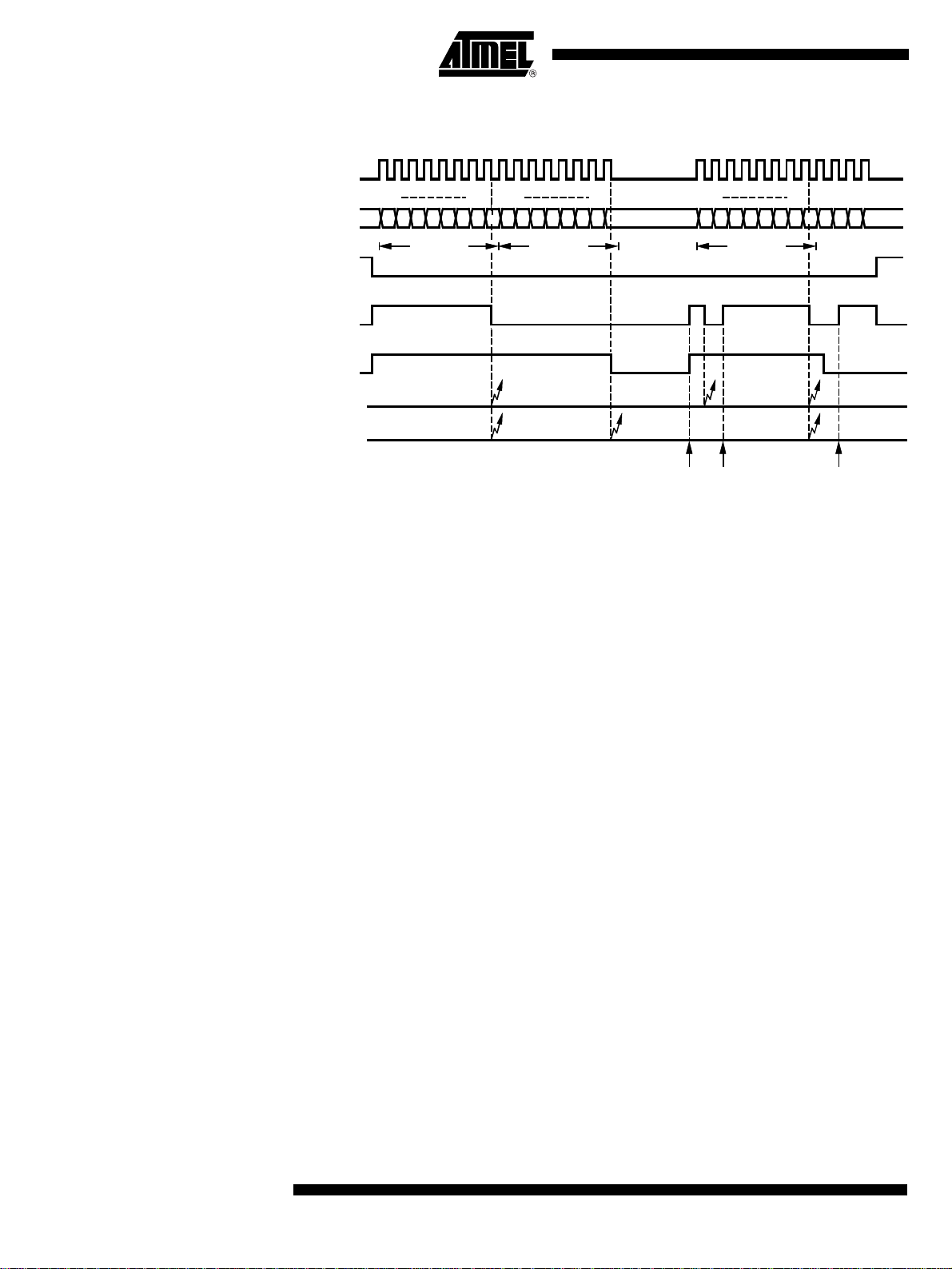
Figure 67. Example of 8-bit Synchronous Receive Operation
SC
SRDY
ACT
Interrupt
(IFN = 0)
Interrupt
(IFN = 1)
SD
SIR
msb
765 43210765 7654
rx data 1 rx data 2 rx data 3
lsb
msb lsb msb lsb
43210 76543210
Read SRB
(rx data 1)
Read SRB
(rx data 2)
Read SRB
(rx data 3)
9-bit Shift Mode (MCL) In the 9-bit shi ft mode, the SSI is able to han dle the MCL protocol described below. It
always operates as an MCL ma ster d evice, i.e ., SC is alw ays gene rated a nd outpu t by
the SSI. Both the MCL sta rt a nd s top co nditi ons are auto matical ly genera ted w hen ever
the SSI is activa ted or d eac tiv at ed by the SI R-bit . In ac c ordanc e wit h th e MCL protocol,
the output data is always changed in the clock low phase and shifted in on the high
phase.
Before activati ng the SSI (S IR = 0) and com mencing an MCL dialog , the appropr iate
data direction for the first word must be set using the SDD control bit. The state of this
bit controls the direction of the data port (BP43 or MCL_SD). Once started, the 8 data
bits are, depending on the selected direction, either clocked into or out of the shift register. During the 9th clock period, the por t direct ion is automa tical ly switc hed ov er so th at
the corresponding acknowledge bit can be shifted out or read in. In transmit mode, the
acknowledge bit received from the device is captured in the SSI Status Register (TACK)
where it can be read by the controller. In receive mode, the state of the acknowledge bit
to be returned to the device is predetermined by the SSI Status Register (RACK).
Changing the directional mode (TX/RX) should not be performed during the transfer of
an MCL telegram. One should wait u ntil the en d of t he telegram whic h ca n be d etecte d
using the SSI interrupt (IFN = 1) or by interrogating the ACT status.
Once started, a 9-bit te legram wi ll al ways run to c ompl etion a nd will not be pre maturely
terminated by the SIR bit. So, if the SIR-bit is set to "1" in telegram, the SSI will complete
the current transfer and terminate the dialog with an MCL stop condition.
70
ATAR862-4
4552B–4BMCU–02/03
Page 71
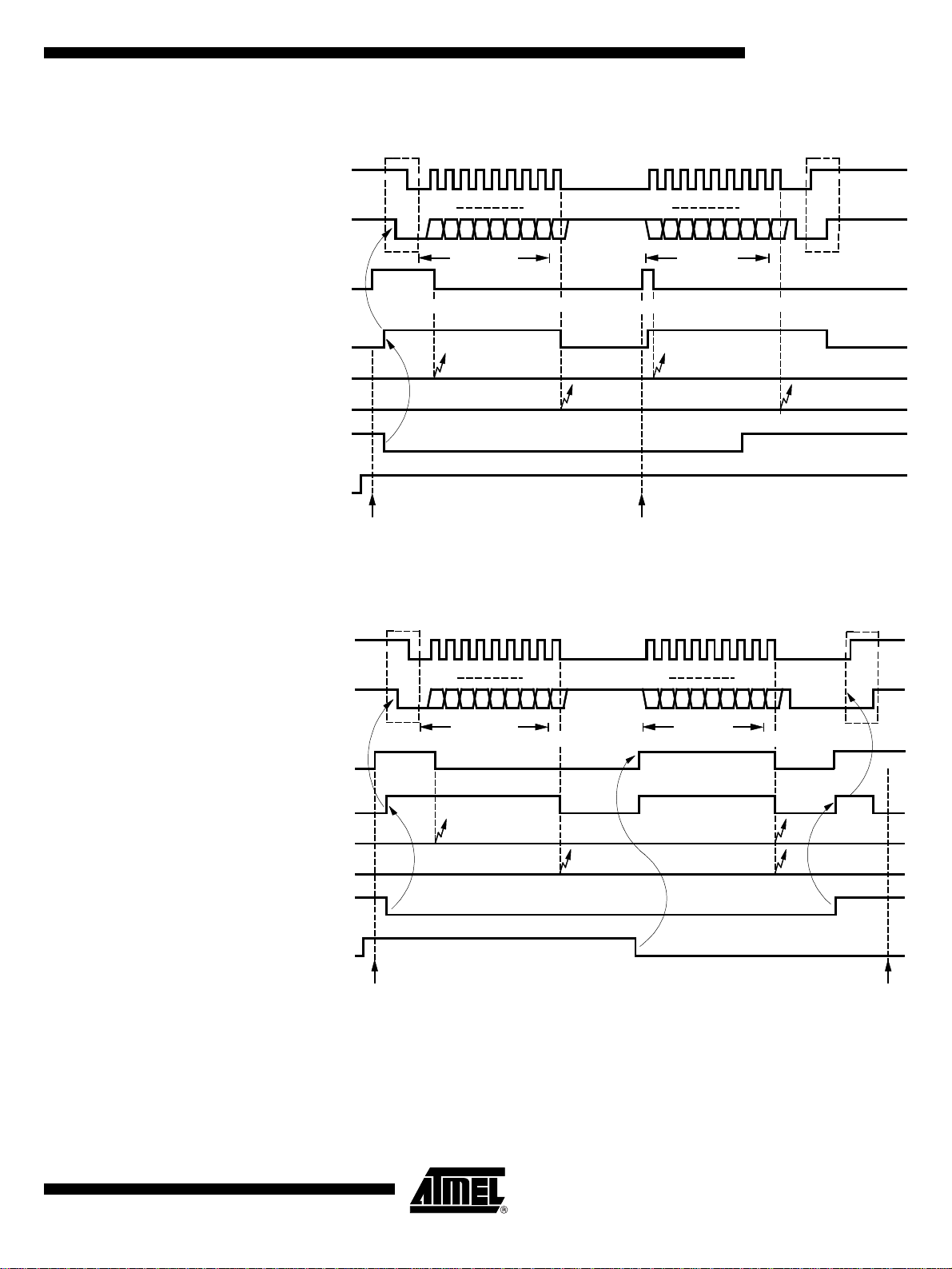
Figure 68. Example of MCL Transmit Dialog
Start Stop
SC
ATAR862-4
lsb
0A
SRDY
ACT
Interrupt
IFN = 0)
Interrupt
IFN = 1)
SDD
SD
SIR
msb
7654321 76543210A
tx data 1 tx data 2
Write STB
(tx data 1)
Figure 69. Example of MCL Receive Dialog
Start
SC
msb lsb
Write STB
(tx data 2)
Stop
SRDY
ACT
Interrupt
(IFN = 0)
Interrupt
(IFN = 1)
SDD
SD
SIR
Write STB
(tx data 1)
msb
7654321 76543210
tx data 1 rx data 2
lsb
0A
msb lsb
A
Read SRB
(rx data 2)
8-bit Pseudo MCL Mode In this mode, the SSI exhibits all the typical MCL operational features except for the
acknowledge-bit which is never expected or transmitted.
4552B–4BMCU–02/03
71
Page 72

MCL Bus Protocol The MCL protoco l constitu tes a simple 2-wir e bi-direc tional com munication hig hway via
which devices can commu nica te cont rol a nd data i nform ation. Altho ugh the M CL pro tocol can support multi-master bu s configurations, the S SI in MCL mode is in tended for
use purely as a master controller on a single master bus system. So all reference to
multiple bus control and bus contention will be omitted at this point.
All data is packaged into 8-bit telegrams plus a trailing handshaking or acknowledge-bit.
Normally the communication channel is opened with a so-called start condition, which
initializes all devices connected to the bus. This is then followed by a data telegram,
transmitted by the m aster controller device. T his telegram u sually co ntains an 8-bi t
address code to activate a single slave device connected onto the MCL bus. Each slave
receives this addr ess and com pares it with its own unique add ress. The addr essed
slave device, if read y to receiv e data, will re spond by pul ling the SD line low during the
9th clock pulse. This represents a so-called MCL acknowledge. The controller detecting
this affirmative acknowledge then opens a connection to the required slave. Data can
then be passed back and forth by the master controller, each 8-bit telegram being
acknowledged by the respective recipient. The communication is finally closed by the
master device and the slave device put back into standby by applying a stop condition
onto the bus.
Figure 70. MCL Bus Protocol 1
(2)(1) (4) (4) (3) (1)
SC
SD
Start
condition
Data
valid
Data
change
Data
valid
Stop
condition
Bus not busy (1) Both data and clock lines remain HIGH.
Start data transfer (2) A HIGH to LOW transition of the SD line while the clock (SC)
is HIGH defines a START condition
Stop data transfer (3) A LOW to HIGH transition of the SD line while the clock (SC)
is HIGH defines a STOP condition.
Data valid (4) The state of the data line represents valid data when,
after START condition, the data line is stable for the
duration of the HIGH period of the clock signal.
Acknowledge All address and data words are serially transmitted to and
from the device in eight-bit words. The receiving device
returns a zero on the data line during the ninth clock cycle to
acknowledge word receipt.
72
ATAR862-4
4552B–4BMCU–02/03
Page 73

Figure 71. MCL Bus Protocol 2
SC
ATAR862-4
1n89
SD
Start
1st Bit 8th Bit ACK Stop
SSI Interrupt The SSI interrupt INT3 can be generated either by an SSI buffer register status (i.e.,
transmit buffer emp ty or receiv e buffer full), th e end of SSI dat a telegra m or on the falling edge of the SC/SD pins on Port 4 (see P4CR). SSI interrupt selection is performed
by the Interrupt F unctioN contr ol bi t (IFN) . Th e SSI in terr upt is u suall y used to synchr onize the software control of the SSI and inform the controller of the present SSI status.
The Port 4 in terrupts can be used to gether with the SSI or, i f the SSI its elf is not
required, as additiona l external inter rupt so urces. In ei ther c ase this interru pt is cap able
of waking the controller out of sleep mode.
To enable and select the SSI relevant interrupts use the SSI interrupt mask (SIM) and
the Interrupt Functi on (IF N) while the Port 4 interr upts ar e enab led by s etting ap prop riate control bits in P4CR register.
Modulation and Demodulation If the shift register is used together with Timer 2 or Timer 3 for modulation or demodula-
tion purposes, the 8-bi t synchron ous mo de mus t be used. In this cas e, the un used P ort
4 pins can be used as conventional bi-directional ports.
The modulation and demodulation stages, if enabled, operate as soon as the SSI is activated (SIR = 0) and cease when deactivated (SIR = 1).
Due to the byte-orientated data control, the SSI (when running normally) generates
serial bit streams which are submultiples of 8 bits. An SSI output masking (OMSK) function permits; h owever, the gener ation of b it stream s of any length . The OMS K signal is
derived indirectly from the 4-bit prescaler of the Timer 2 and masks out a programmable
number of unrequired trailing data bits during the shifting out of the final data word in the
bit stream. The number of non-masked data bits is defined by the value pre-programmed in the presca ler c omp ar e regi ste r. To use outp ut ma sk in g, the modu la tor sto p
mode bit (MSM) must be set to "0" be fore prog rammi ng the final data wor d into th e SSI
transmit buffer. This in tu rn, enabl es shif t clock s to the p rescal er when th is final word is
shifted out. On reaching the compare value, the prescaler triggers the OMSK signal and
all following data bits are blanked.
Internal 2-wire Multi-chip Link Two additional on-chip pads (MCL_SC and MCL_SD) for the SC and the SD line can be
used as chip-to-chip link for multi-chip applications. These pads can be activated by setting the MCL-bit in the SISC-register.
73
4552B–4BMCU–02/03
Page 74

Figure 72. Multi-chip Link
SCL SDA
MCL_SC MCL_SD
V
DD
BP40/SC
Microcontroller
BP10
Figure 73. SSI Output Masking Function
U505M
Multi chip link
V
SS
BP43/SD
BP13
Serial Inte rface Registers
Serial Interface Control Register 1 (SIC1)
TOG2
POUT
T1OUT
SYSCL
SCL
CL2/1
SC
/2
4-bit counter 2/1
Compare 2/1
SO
Shift_CL
CM1
SSI-control
MSB LSB
8-bit shift register
Timer 2
OMSK
Control
SI
Auxiliary register address: "9"hex
Bit 3 Bit 2 Bit 1 Bit 0
SIR SCD SCS1 SCS0 Reset value: 1111b
SIR S
erial Interface Reset
SIR = 1, SSI inactive
SIR = 0, SSI active
SO
Output
74
ATAR862-4
SCD Serial Clock Direction
SCD = 1, SC line used as output
SCD = 0, SC line used as input
Note: This bit has to be set to "1" during the MCL mode and the Timer 3 mode 10 or 11
SCS1 Serial Clock source Select bit 1 SCS1 SCS0 Internal Clock for SSI
SCS0 S
erial Clock source Select bit 0 1 1 SYSCL/2
1 0 T1OUT/2
Note: with SCD = "0" the bits SCS1 0 1 POUT/2
and SCS0 are insignificant 0 0 TOG2/2
4552B–4BMCU–02/03
Page 75
ATAR862-4
• In Transmit mode (SDD = 1) shifting starts only if the transmit buffer has been
loaded (SRDY = 1).
• Setting SIR-bit loads the contents of the shift register into the receive buffer
(synchronous 8-bit mode only).
• In MCL modes, writing a 0 to SIR generates a start condition and writing a 1
generates a stop condi tion.
Serial Interface Control Register 2 (SIC2)
Auxiliary register address: "A"hex
Bit 3Bit 2Bit 1Bit 0
MSM SM1 SM0 SDD Reset value: 1111b
MSM M
SM1 Serial Mode control bit 1
SM0 S
Mode SM1 SM0 SSI Mode
1 1 1 8-bit NRZ-Data changes with the rising edge of SC
2 1 0 8-bit NRZ-Data changes with the falling edge of SC
3 0 1 9-bit tw o-wire MCL mode
4 0 0 8-bit two-wire MCL mode (no acknowledge)
SDD Serial Data Direction
Note: SDD controls port directional control and defines the reset function for the SRDY-flag
odular Stop Mode
MSM = 1, modulator stop mode disabled (output masking off)
MSM = 0, modulator stop mode enabled (output masking on) - used in
modulation modes for generating bit streams which are not sub–multiples of 8
bits.
erial Mode control bit 0
SDD = 1, transmit mode
SDD = 0, receive mode
– SD line used as output (transmit data). SRDY is set
by a transmit buffer write access.
– SD line used as input (receive data). SRDY is set
by a receive buffer read access
4552B–4BMCU–02/03
75
Page 76

Serial Interface Status and Control Register (SISC)
Primary register address: "A"hex
Bit 3 Bit 2 Bit 1 Bit 0
Write MCL RACK SIM IFN Reset value: 1111b
Read - - - TACK ACT SRDY Reset value: xxxxb
MCL M
RACK Receive ACKnowledge status/control bit for MCLmode
TACK Transmit ACKnowledge status/control bit for MCL mode
SIM Serial Interrupt Mask
IFN Interrupt FuNction
SRDY Serial interface buffer ReaDY status flag
ACT Transmission ACTive status flag
ulti-Chip Link activation
MCL = 1,multi-chip link d isa bled.
transactions to/from EEPR OM of the M44C892
MCL = 0, connects SC and SD additionally to the internal multi-chip link pads
RACK = 0, transmit acknowledge in next receive telegram
RACK = 1, transmit no acknowledge in last receive telegram
TACK = 0, acknowledge received in last transmit telegram
TACK = 1, no acknowledge received in last transmit telegram
SIM = 1, disable interrupts
SIM = 0, enable serial interrupt. An interrupt is generated.
IFN = 1, the serial interrupt is generated at the end of telegram
IFN = 0, the serial interrupt is generated when the SRDY goes low (i.e., buffer
becomes empty/full in transmit/receive mode)
SRDY = 1, in receive mode: receive buffer empty
in transmit mode: tran smit buf fer full
SRDY = 0, in receive mode: receive buffer full
in transmit mode: trans mi t b uffer empty
ACT = 1, transmission is active, i.e., serial data transfer. Stop or start conditions
are currently in progress.
ACT = 0, transmission is inactive
This bit has to be set to "0" during
Serial Transmit Buffer (STB) – Byte Write
Serial Receive Buffer (SRB) – Byte Read
76
ATAR862-4
Primary register address: "9"hex
First write cycle Bit 3 Bit 2 Bit 1 Bit 0 Reset value: xxxxb
Second write cycle Bit 7 Bit 6 Bit 5 Bit 4 Reset value: xxxxb
T
he STB is the transmit buffe r of th e SSI. T he SSI t r ansfers the tran sm it b uffe r into the shift regis-
ter and star
ts shifting with the most significant bit.
Primary register address: "9"hex
First read cycle Bit 7 Bit 6 Bit 5 Bit 4 Reset value: xxxxb
Second read cycle B it 3 Bit 2 B it 1 Bit 0 Reset value: xxxxb
he SRB is the receive buffer of the SSI. The shift register clocks serial data in (most significant
T
bit first) and loads content into the receive buffer when complete telegram has been received.
4552B–4BMCU–02/03
Page 77

ATAR862-4
Combination Modes The UTCM consists of two timers (Timer 2 an d Timer 3) and a ser ial interfa ce. Th ere is
a multitude of modes in which the timers and serial interface can work together.
The 8-bit wide serial interface operates as shift register for modulation and demodula-
tion. The modulator and demodulator units work together with the timers and shi ft the
data bits into or out of the shift register.
Combination Mode Timer 2 and SSI
Figure 74. Combination Timer 2 and SSI
I/O-bus
T2I
SYSCL
T1OUT
TOG3
SCL
T2C
CL2/1
I/O-bus
4-bit counter 2/1
RES OVF1
Compare 2/1
T2CO1
POUT
Timer 2 - control
POUT
TOG2
CM1
T2M1P4CR
CL2/2
DCG
DCGO
8-bit counter 2/2
RES OVF2
TOG2
Compare 2/2
INT4
T2CO2T2CM
T2M2
Output
MOUT
Biphase-,
Manchester-
modulator
SO Control
T2O
Timer 2
modulator
output-stage
POUT
T1OUT
SYSCL
SIC1 SIC2 SISC
TOG2
SCLI
SCL
Shift_CL
SSI-control
SO
MSB LSB
STB SRB
Transmit
buffer
8-bit shift register
I/O-bus
Control
Receive
buffer
SI
INT3
Output
SO
MCL_SC
MCL_SD
SC
SD
4552B–4BMCU–02/03
77
Page 78

Combination Mode 1: Burst Modulation
SSI mode 1: 8-bit NRZ and internal data SO output to the Timer 2
modulator stage
Timer 2 mode 1, 2, 3 or 4: 8-bit compare counter with 4-bit programmable prescaler
and DCG
Timer 2 output mode 3: Duty cycle burst generator
Figure 75. Carrier Frequency Burst Modulation with the SSI Internal Data Output
DCGO
Counter 2
TOG2
1 201201201201201201201201201201201201201
Counter = compare register (=2)
Combination Mode 2: Biphase Modulation 1
SO
T2O
Bit 0 Bit 1 Bit 2 Bit 3 Bit 4 Bit 5 Bit 6 Bit 7 Bit 8 Bit 9 Bit 10 Bit 11 Bit 12 Bit 13
SSI mode 1: 8-bit shift register internal data output (SO) to the Timer 2
modulator stage
Timer 2 mode 1, 2, 3 or 4: 8-bit compare counter with 4-bit programmable prescaler
Timer 2 output mode 4: The modulator 2 of Timer 2 modulates the SSI internal
data output to Biphase code
Figure 76. Biphase Modulation 1
TOG2
SC
SO
T2O
00110101
Bit 7 Bit 0
0000
Data: 00110101
1111
8-bit SR-data
78
ATAR862-4
4552B–4BMCU–02/03
Page 79

ATAR862-4
Combination Mode 3: Manchester Modulation 1
Combination Mode 4: Manchester Modulation 2
SSI mode 1: 8-bit shift register internal data output (SO) to the Timer 2
modulator stage
Timer 2 mode 1, 2, 3 or 4: 8-bit compare counter with 4-bit programmable prescaler
Timer 2 output mode 5: The modulator 2 of Timer 2 modulates the SSI internal
data output to Manchester code
Figure 77. Manchester Modulation 1
TOG2
SC
SO
T2O
00110101
Bit 7 Bit 0
0
Bit 7 Bit 0
Data: 00110101
11 1 1
8-bit SR-data
000
SSI mode 1: 8-bit shift register internal data output (SO) to the Timer 2
modulator stage
Timer 2 mode 3: 8-bit compare counter and 4-bit prescaler
Timer 2 output mode 5: The modulator 2 of Timer 2 modulates the SSI data output
to Manchester code
The 4-bit stage can be used as prescaler for the SSI to generate the stop signal for modulator 2. The SSI has a s pecial mode to supply the pr escaler with th e shift clock. The
control output signal ( OMSK ) of th e SSI i s us ed as sto p s ign al for the mod ula tor . F igur e
70 shows an example for a 12-bit Manchester telegram.
Figure 78. Manchester Modulation 2
SCLI
Buffer full
SIR
Bit 7 Bit 6 Bit 5 Bit 4 Bit 3 Bit 2 Bit 1 Bit 0 Bit 7 Bit 6 Bit 5 Bit 4 Bit 3 Bit 2 Bit 1 Bit 0
0000000012340120
Counter 2/1 = Compare Register 2/ 1 (= 4)
3
Counter
SO
SC
MSM
Timer 2
Mode 3
SCL
2/1
OMSK
T2O
4552B–4BMCU–02/03
79
Page 80

Combination Mode 5: Biphase Modulation 2
SSI mode 1: 8-bit shift register internal data output (SO) to the Timer 2
modulator stage
Timer 2 mode 3: 8-bit compare counter and 4-bit prescaler
Timer 2 output mode 4: The modulator 2 of Timer 2 modulates the SSI data output
to Biphase code
The 4-bit stage can be used as prescaler for the SSI to generate the stop signal for modulator 2. The SSI has a special mode to supply the prescaler via the shift clock. The
control output signal ( OMSK ) of th e SSI i s us ed as sto p s ign al for the mod ula tor . F igur e
71 shows an example for a 13-bit Biphase telegram.
Figure 79. Biphase Modulation
SCLI
Buffer full
SIR
Bit 7 Bit 6 Bit 5 Bit 4 Bit 3 Bit 2 Bit 1 Bit 0 Bit 7 Bit 6 Bit 5 Bit 4 Bit 3 Bit 2 Bit 1 Bit 0
00000000123450
Counter 2/1 = Compare Register 2/ 1 (= 5)
012
Counter
SO
SC
MSM
Timer 2
Mode 3
SCL
2/1
OMSK
T2O
80
ATAR862-4
4552B–4BMCU–02/03
Page 81
Combination Mode Timer 3 and SSI
Figure 80. Combination Timer 3 and SSI
ATAR862-4
I/O-bus
T3MT3CS
T3I
T3EX
SYSCL
T1OUT
POUT
CL3
RES
Compare 3/1
T3CO1
T3CP
8-bit counter 3
TOG2
POUT
T1OUT
SYSCL
CP3
Compare 3/2
T3CO2
SIC1 SIC2
SCLI
Shift_CL
Transmit buffer Receive buffer
T3C T3ST
Timer 3 - control
T3CM1 T3CM2
SSI-control
SO
8-bit shift register
MSB LSB
STB SRB
I/O-bus
SISC
Control
INT3
SI
T3EX
T3I
CM31
RES
INT5
TOG3
SO
Control
M2
SI
Output
SC
Demodu-
lator 3
Modulator 3
MCL_SC
MCL_SD
SC
SI
T3O
SC
SI
Combination Mode 6: FSK Modulation
4552B–4BMCU–02/03
SSI mode 1: 8-bit shift register internal data output (SO) to the Timer 3
Timer 3 mode 8: FSK modulation with shift register data (SO)
The two compare registers are used to generate two varied time intervals. The SSI data
output selects which compare register is used for the output frequency generation. A "0"
level at the SSI data output enab les the compare r egister 1 an d a "1" lev el enable s the
compare register 2. The compare and compare mode registers must be programmed to
generate the two frequencies via the output toggle flip-lop. The SSI can be supplied with
the toggle signal of Tim er 2 or any other clock source. The T imer 3 c ounter is driven by
an internal or external clock source.
81
Page 82

Figure 81. FSK Modulation
T3R
Counter 3
CM31
CM32
01234012340120
12012012012012012012012340
12
3
40
Combination Mode 7: Pulse-width Modulation (PWM)
SO
T3O
01 0
SSI mode 1: 8-bit shift register internal data output (SO) to the Timer 3
Timer 3 mode 9: Pulse-width modulation with the shift register data (SO)
The two compare registers are used to generate two varied time intervals. The SSI data
output selects wh ich comp are regi ster i s used fo r the o utput puls e gener ation. In th is
mode, both compare and compare mode registers must be programmed to generate the
two pulse width. It is a lso useful to enabl e the sing le-action mode for extreme d uty
cycles. Timer 2 is used as baudrate generator and for the triggered restart of Timer 3.
The SSI must be supplied with the toggle si gnal of Tim er 2. The counter is driven by an
internal or external clock source.
Figure 82. Pulse-width Modulation
TOG2
SIR
SO
SCO
T3R
Counter 3
000000000 0000
00000123456789101112131415012345
00 1
67819111210 1413 0 2 314150
Combination Mode 8: Manchester Demodulation/ Pulse-width Demodulation
82
ATAR862-4
CM31
CM32
T3O
SSI mode 1: 8-bit shift register internal data input (SI) and the internal shift clock
(SCI) from the Timer 3
Timer 3 mode 10: Manchester demodulation/pulse-width demodulation with Timer 3
For Manchester demodula tion , the edge detec ti on sta ge mus t be progr am me d to detec t
each edge at the input. These edges are evaluated by the demodulator stage. The timer
stage is used to gene rate the sh ift clock for the SSI. A compare r egister 1 match even t
defines the correct moment for shifting the state from the input T3I as the decoded bit
into shift register. Af ter that, the dem odulat or waits for the next ed ge to syn chroni ze the
timer by a reset for the next bit. The c ompare reg ister 2 ca n be used to detec t a time
error and handle it with an interrupt routine.
4552B–4BMCU–02/03
Page 83
ATAR862-4
Before activating the demodulator mode the timer and the demodulator stage must be
synchronized with t he bits tream. T he M ancheste r co de tim ing c onsists o f p arts wit h th e
half bitlength and the complete bitlength. A synchronization routine must start the
demodulator after an interval with the complete bitlength.
The counter can be driven by any internal clock source. The output T3O can be used by
Timer 2 in this mode. The Manchester decoder can also be used for pulse-width demodulation. The input must programmed to detect the positive edge. The demodulator and
timer must be synchroni zed with the lea ding edge of the pulse. After that a counter
match with the compare register 1 shifts the state at the inp ut T3I into the shift reg ister.
The next positive edge at the input restarts the timer.
Figure 83. Manchester Demodulation
Combination Mode 9: Biphase Demodulation
Timer 3
mode
T3I
T3EX
SI
CM31=SCI
SR-DATA
Synchronize Manchester demodulation mode
1011100110
11
Bit 7 Bit 6 Bit 5 Bit 4 Bit 3
100110
Bit 2 Bit 1
Bit 0
SSI mode 1: 8-bit shift register internal data input (SI) and the internal shift clock
(SCI) from the Timer 3
Timer 3 mode 11: Biphase demodulation with Timer 3
In the Biphase demodulation mode the timer works like in the Manchester demodulation
mode. The difference is that the bits are decoded with the toggle flip-flop. This flip-flop
samples the edge in the middle of the bi tframe and the compar e registe r 1 match event
shifts the toggle flip-flop output into shift register. Before activating the demodulation the
timer and the demodulation stage must be synchronized with the bitstream. The
Biphase code timing c onsists of parts wit h the half bitleng th and the c omple te bitle ngth.
The synchronization routine must start the demodulator after an interval with the complete bitlength.
4552B–4BMCU–02/03
The counter can be driven by any internal clock source and the output T3O can be used
by Timer 2 in this mode.
83
Page 84

Figure 84. Biphase Demodulation
Timer 3
mode
T3I
T3EX
Q1=SI
CM31=SCI
Reset
Counter 3
SR-DATA
Combination Mode Timer 2 and Timer 3
Figure 85. Combination Timer 3 and Timer 2
I/O-bus
T3CS T3M
Synchronize Biphase demodulation mode
011 1 1
0000
01
101010
Bit 7 Bit 6 Bit 5 Bit 4 Bit 3 Bit 2 Bit 1
Bit 0
T3I
T2I
T3EX
SYSCL
T1OUT
POUT
TOG3
SYSCL
T1OUT
SCL
T2C
CL3
RES
Compare 3/1
CL2/1
I/O-bus
T3CP
8-bit counter 3
Compare 3/2
T3CO1
4-bit counter 2/1
RES OVF1
Compare 2/1
T2CO1
CM1
T3CO2
SSI
CP3
POUT
Timer 2 - control
POUT
T3C T3ST
Timer 3 - control
T3CM1 T3CM2
T2M1P4CR
CL2/2
DCG
DCGO
8-bit counter 2/2
RES OVF2
Compare 2/2
T2CO2T2CM
TOG2
I/O-bus
TOG2
INT4
T3EX
T3I
CM31
RES
INT5
TOG3
Control
SO
M2
SO
Control
(RE, FE, SCO, OMSK)
SSI
Demodu-
lator 3
Modulator 3
T2M2
OUTPUT
MOUT
Biphase-,
Manchester-
modulator
SCI
SI
SSI
M2
modulator 2
output-stage
T3O
T2O
Timer 2
84
ATAR862-4
4552B–4BMCU–02/03
Page 85

ATAR862-4
Combination Mode 10: Frequency Measurement or Event Counter with Time Gate
Timer 2 mode 1/2: 12-bit compare counter/8-bit compare counter and
4-bit prescaler
Timer 2 output mode 1/6: Timer 2 compare match toggles (TOG2) to the Timer 3
Timer 3 mode 3: Timer/Counter; internal trigger restart and internal
capture (with Timer 2 TOG2-signal)
The counter is driven by an external (T3I) clock source. The output signal (TOG2) of
Timer 2 resets the counter. The counter value before reset is saved in the capture register. If single-action mode is ac tivated for on e or both comp are register s, the trigger
signal restarts also the single actions. This mode can be used for frequency measurements or as event counter with time gate.
Figure 86. Frequency Measurement
T3R
T3I
ounter 3
TOG2
T3CP-
Register
0012345678910
Capture value = 0 Capture value = 17
11121314151617 1234567891011121314151617180 012345
Capt. value = 18
Figure 87. Event Counter with Time Gate
Combination Mode 11: Burst Modulation 1
T3R
T3I
Counter 3
TOG2
T3CP-
Register
0012345678910
Capture value = 0 Capture value = 11
11 0 1 2 401
3
2
Cap. val. = 4
Timer 2 mode 1/2: 12-bit compare counter/8-bit compare counter and
4-bit prescaler
Timer 2 output mode 1/6: Timer 2 compare match toggles the output flip-flop (M2)
to the Timer 3
Timer 3 mode 6: Carrier frequency burst modulation controlled by Timer 2
output (M2)
The Timer 3 counter is driven by an internal or external clock source. Its compare and
compare mode register s must be program med to generate the carrier freq uency with
the output toggle flip-flop. The output toggle flip-flop (M2) of Timer 2 is used to enable
and disable the Timer 3 output. The Timer 2 can be driven by the toggle output signal of
Timer 3 (TOG3) or any other clock source.
4552B–4BMCU–02/03
85
Page 86

Figure 88. Burst Modulation 1
CL3
Counter 3
Counter 2/2
0101234501012345010 123 450101 50101 50101 50101 50101 50101 50101 50101 50101 50101
CM1
CM2
TOG3
M3
30 1 2 3 3 0 1 32
TOG2
M2
T3O
86
ATAR862-4
4552B–4BMCU–02/03
Page 87

Combination Mode Timer 2, Timer 3 and SSI
Figure 89. Combination Timer 2, Timer 3 and SSI
I/O-bus
T3CS T3M
ATAR862-4
T3I
T2I
T3EX
SYSCL
T1OUT
POUT
TOG3
SYSCL
T1OUT
SCL
T2C
CL3
RES
Compare 3/1
T3CO1
CL2/1
RES OVF1
I/O-bus
T3CP
8-bit Counter 3
4-bit Counter 2/1
Compare 2/1
T2CO1
TOG2
POUT
T1OUT
SYSCL
CP3
T3C T3ST
Compare 3/2
T3CO2
CL2/2
POUT
Timer 3 - control
T3CM1 T3CM2
T2M1P4CR
DCG
Timer 2 - control
CM1
POUT
T2CM
SIC1 SIC2 SISC
SCLI
SCL
SO
Shift_CL
SSI-control
8-bit shift register
MSB LSB
DCGO
8-bit Counter 2/2
RES OVF2
Compare 2/2
T2CO2
TOG2
I/O-bus
TOG2
INT4
Control
(RE, FE,
SCO, OMSK)
SI
INT3
TOG3
Control
T3EX
T3I
CM31
RES
INT5
Output
SO
SO
Control
M2
Demodu-
lator 3
Modulator 3
T2M2
OUTPUT
MOUT
M2
Biphase-,
Manchester-
modulator
Timer 2
modulator 2
output-stage
MCL_SC
MCL_SD
SCI
SI
T3O
SSI
T2O
SC
SI
4552B–4BMCU–02/03
Transmit buffer
STB
I/O-bus
SRB
Receive buffer
87
Page 88

Combination Mode 12: Burst Modulation 2
Figure 90. Burst Modulation 2
CL3
Counter 3
Counter 2/2
0101234501012345010123450101 50101 50101 50101 50101 50101 50101 50101 50101 50101
CM31
CM32
TOG3
M3
30 1 2 3 3 0 1 32
TOG2
SO
T3O
SSI mode 1: 8-bit shift register internal data output (SO) to the Timer 3
Timer 2 output mode 2: 8-bit compare counter and 4-bit prescaler
Timer 2 output mode 1/6: Timer 2 compare match toggles (TOG2) to the SSI
Timer 3 mode 7: Carrier frequency burst modulation controlled by the internal
output (SO) of SSI
The Timer 3 counter is driven by an internal or external clock source. Its compare and
compare mode register s must be program med to generate the carrier freq uency with
the output toggle flip-flop (M3). The internal data output (SO) of the SSI is used to
enable and disable the Timer 3 output. The SSI can be supplied with the toggle signal of
Timer 2.
Combination Mode 13: FSK Modulation
SSI mode 1: 8-bit shift register internal data output (SO) to the Timer 3
Timer 2 output mode 3: 8-bit compare counter and 4-bit prescaler
Timer 2 output mode 1/6: Timer 2 4-bit compare match signal (POUT) to the SSI
Timer 3 mode 8: FSK modulation with shift register data output (SO)
The two compare registers are used to generat e two different time interval s. The SSI
data output selects wh ic h c om pare r e gis ter i s us ed f or the outp ut f re que ncy generation.
A "0" level at the SSI data output enables the compare register 1 and a "1" level enables
the compare reg ister 2. The c ompare- and com pare mode r egisters must be programmed to generate the two frequencies via the output toggle flip-flop. The SSI can be
supplied with the toggle signal of Timer 2 or any other clock source. The Timer 3 counter
is driven by an internal or external clock source.
88
ATAR862-4
4552B–4BMCU–02/03
Page 89
Figure 91. FSK Modulation
T3R
Counter 3
CM31
CM32
01234012340123
ATAR862-4
40120120120120120120120123
40
1
SO
T3O
01 0
Microcontroller Block The microc ont ro ll er bl ock i s a mu lti ch ip devic e whi ch offe rs a com bi nati on of a MA RC4-
based microcontroller and a serial E2PROM data memory in a single package. A microcontroller is used and as s erial E2 PRO M the U 505M . T wo i nte rnal l in es ca n be u se d as
chip-to-ch ip link in a s ingle pa ckage. Th e maximum i nternal data comm unicati on frequency between the microcontroller block and the U505M over the chip link (MCL_SC
and MCL_SD) is f
The microcontroller and the EEPROM portions of this multi-chip device are equivalent to
their respective individual component chips, except for the electrical specification.
Internal 2-wire Multi-chip Link Two additional on-chip pads (MCL_SC and MCL_SD) for the SC and the SD line can be
used as chip-to-chip link for multi-chip applications. These pads can be activated by setting the MCL-bit in the SISC-register.
Figure 92. Link between the Microcontroller Bloc k and U505 M
SC_MCL
= 500 kHz.
MCL_SC MCL_SD
V
DD
BP40/SC
BP10
U505M
SCL SDA
Microcontroller
Multi chip link
V
SS
BP43/SD
BP13
U505M EEPROM The U505M is a 5 12-bit E EPROM internal ly orga nized as 32 x 16-bi ts. The progra m-
ming voltage as well as the write-cycle timing is generated on-chip. The U505M features
a serial interface allo wing oper ation on a sim ple two-w ire bus with an MCL protocol . Its
low power consumption makes it well suited for battery applications.
89
4552B–4BMCU–02/03
Page 90

Figure 93. Block Diagram EEPROM
V
DD
V
SS
Address
control
HV-generatorTiming control
EEPROM
32 x 16
Mode
control
SCL
I/O
control
SDA
16-bit read/write buffer
8-bit data register
Serial Interface The U505M has a two-wire serial interface (TWI) to the microcontroller for read and
write accesses to the EEPROM. The U505M is considered to be a slave in all these
applications. That mean s, the controller has to be the mas ter that initiates the data
transfer and provides the clock for transmit and receive operations.
The serial interface is contr olled by the mic rocont roller block whi ch ge nerates th e seria l
clock and controls the access via the SCL-line and SDA-line. SCL is used to clock the
data into and out of the device. SDA is a bi-directional line that is used to transfer data
into and out of the device. The following protocol is used for the data transfers.
Serial Protocol • Data states on the SDA-line changing only while SCL is low.
• Changes on the SDA-line while SCL is high are interpreted as START or STOP
condition.
• A START condition is defined as high to low transition on the SDA-line while the
SCL-line is high.
• A STOP condition is defined as low to high transition on the SDA-line while the SCLline is high.
• Each data transfer must be initialized with a STAR T condition and terminated with a
STOP condition. The STAR T condition wakes the device from standby mode and the
STOP condition returns the device to standby mode.
• A receiving device generates an acknowledge (A) after the reception of each byte.
This requires an additional clock pulse, generated by the master. If the reception
was successful the receiving master or slave device pulls down the SDA-line during
that clock cycle. If an acknowledge is not detected (N) by the interface in transmit
mode, it will terminate further data transmissions and go into receive mode. A
master device must finish its read operation by a non-acknowledge and then send a
stop condition to bring the device into a known state.
90
ATAR862-4
4552B–4BMCU–02/03
Page 91
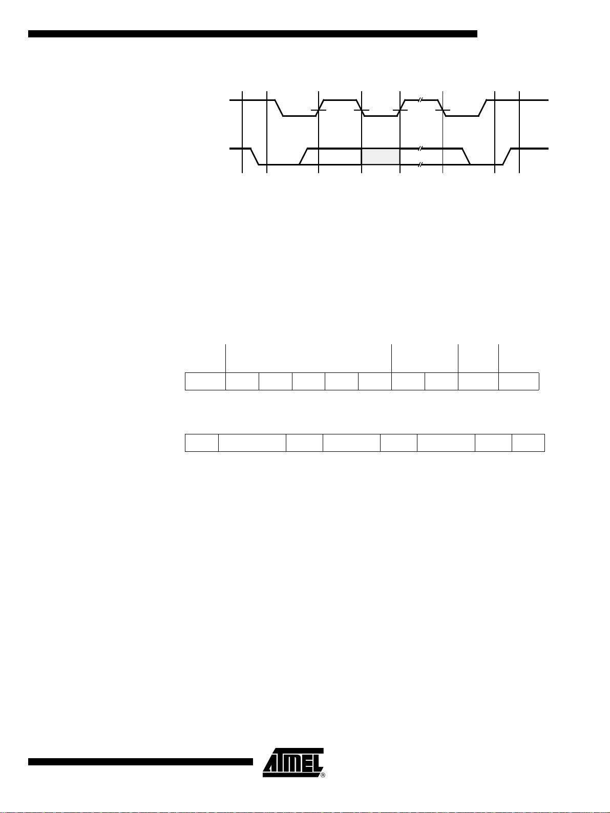
Figure 94. MCL Protocol
SCL
SDA
ATAR862-4
Control Byte Format
Stand
by
Start
condition
Data
valid
Data
change
Data/
acknowledge
valid
Stop
condition
Stand-
by
• Before the START condition and after the STOP condition the device is in standby
mode and the SDA line is switched as input with pull-up resistor.
• The control byte that follows the START condition determines the following
operation. It consists of the 5-bit row address, 2 mode control bits and the
READ/NWRITE bit that is used to control the direction of the following transfer . A "0"
defines a write access and a "1" a read access.
EEPROM Address Mode
Control Bits
StartA4A3A2A1A0C1C0R/NWAckn
Start Control byte Ac kn Data byte Ackn Data by te Ackn Stop
Read/
NWrite
EEPROM The EEPROM has a size of 512 bits and is organized as 32 x 16-bit matrix. To read and
write data to and from the EEPROM the serial interface must be used. The interface
supports one and two byte write accesses and one to n-byte read accesses to the
EEPROM.
EEPROM – Operating Modes The operatin g modes of the EEPROM are defined via the control b yt e. The control byte
contains the row address, the mode control bits and the read/not-write bit that is used to
control the direction of the following transfer . A "0" defines a write acc ess and a "1" a
read access. The five address bits select one of the 32 rows of the EEPROM memory to
be accessed. For all accesses the c omplete 16-bit word of the se lected row is loaded
into a buffer. The buffer must be read or overwritten via the serial interface. The two
mode control bits C1 and C2 define in which order the accesses to the buffer are performed: High byte – low byte or low byte – high byte. The EEPROM also supports
autoincrement and autodecrement read operations. After sending the start address with
the corresponding mode, consecutive memory cells can be read row by row without
transmission of the row addresses.
Two special con trol bytes enable the complete i nitializat ion of EEP ROM with " 0" or
with "1".
91
4552B–4BMCU–02/03
Page 92

Write Operations The EEPROM permits 8-bit and 16-bit write operations. A write acces s starts with the
START conditio n followed by a writ e control byte an d one or two data by tes from the
master. It is completed via the STOP condition from the master after the acknowledge
cycle.
The programming cycle consists of an erase cycle (write "zeros") and the write cycle
(write "ones"). Both cycles together take about 10 ms.
Acknowledge Polling If the EEPROM is busy with an internal write cycle, all inputs are disabled and the
EEPROM will not acknowle dge until the write cyc le is finished. T his can be used to
detect the end of the write cycle. The maste r must perform acknowledge polling by
sending a start condition followed by the control byte. If the device is still busy with the
write cycle, it will not return an acknowledge and the master has to generate a stop condition or perform further acknowledge polling sequences. If the cy cle is complete, it
returns an acknowledge and the master can proceed with the next read or write cycle.
Write One Data Byte
Start Control byte A Data byte 1 A Stop
Write Tw o Data Bytes
Start Control byte A Data byte 1 A Data byte 2 A Stop
Write Control Byte Only
Start Control byte A Stop
Write Control Bytes
MSB LSB
Write low byte first A4 A3 A2 A1 A0 C1 C0 R/NW
Row address 0 1 0
Byte order LB(R) HB(R)
MSB LSB
Write high byte first A4 A3 A2 A1 A0 C1 C0 R/NW
Row address 1 0 0
Byte order HB(R) LB(R)
A -> acknowledge; HB -> high byte; LB -> low byte; R -> row address
Read Operations The EEP ROM allows byte- , word- and cu rren t address read opera tions . The read ope r-
ations are initiated in the same way as write operations. Every read access is initiated by
sending the START condition followed by the control byte which contains the address
and the read mode. When the device has received a read command, it returns an
acknowledge, l oads the addresse d word into the rea d/write buffer an d sends the
selected data byte to the m aster . The ma ster has to acknow ledge th e rec eived byt e if it
wants to proceed the read operation. If two bytes are read out from the buffer the device
increments respectively decrements the word address automatically and loads the
buffer with the next wo rd. The read mod e bits de termi nes if th e low o r high b yte is r ead
first from the buffer and if t he word address is increm ented or decrem ented for the next
92
ATAR862-4
4552B–4BMCU–02/03
Page 93

Read One Data Byte
Read Two Data Bytes
Read n Data Bytes
Read Control Bytes
ATAR862-4
read access. If the memory address limit is reached, the data word address will roll over
and the sequential read will continue. The master can terminate the read operation after
every byte by not responding with an acknowledge (N) and by issuing a stop condition.
Start Control byte A Data byte 1 N Stop
Start Control byte A Data byte 1 A Data byte 2 N Stop
Start Control byte A Data byte 1 A Data byte 2 A – Data byte n N Stop
MSB LSB
Initialization After a Reset Condition
Read low byte first,
address increment
Byte order LB(R) HB(R) LB(R+1) HB(R+1) - - - LB(R+n) HB(R+n)
Read high byte first,
address decrement
Byte order HB(R) LB(R) HB(R-1) LB(R-1) - - - HB(R-n) LB(R-n)
A4 A3 A2 A1 A0 C1 C0 R/NW
Row address 0 1 1
MSB LSB
A4 A3 A2 A1 A0 C1 C0 R/NW
Row address 1 0 1
A -> acknowledge, N -> no acknowledge; HB -> high byte; LB -> low byte,
R -> row address
The EEPROM with the serial interface has its own reset circuitry. In systems with microcontrollers that have their own rese t circuitry for power -on reset, watc hdog reset or
brown-out reset, it may be necessary to bring the U505M into a known state independent of its internal reset. This is performed by writing:
4552B–4BMCU–02/03
Start Control byte A Data byte 1 N Stop
to the serial interface. If the U505 M ac knowl edg es thi s seq uenc e i t is i n a de fin ed s tat e.
Maybe it is necessary to perform this sequence twice.
93
Page 94

Absolute Maximum Ratings
Voltages are given relative to V
SS
Parameters Symb ol Value Unit
Supply voltage V
Input voltage (on any pin) V
Output short circuit duration t
Operating temperature range T
Storage temperature range T
Soldering temperature (t £ 10 s) T
DD
IN
short
amb
stg
sld
-0.3 to +4.0 V
VSS -0.3 £ VIN £ VDD +0.3 V
Indefinite s
-40 to +125 °C
-40 to +130 °C
260 °C
Note: Stresses greater than those listed under absolute maximum ratings may cause permanent damage to the device. This is a
stress rating only and functional operation of the device at any condition above those indicated in the operational section of this
specification is not implied. Exposure to absolute maximum rating condition for an extended period may affect device reliability.
All inputs and outputs are protected against high electrostatic voltages or electric fields. However, precautions to minimize the
build-up of electrostatic charges during handling are recommended. Reliability of operation is enhanced if unused inputs are
connected to an appropriate logic voltage level (e.g., V
DD
).
Thermal Resistance
Parameter Symbol V alue Unit
Thermal resistance (SSO20) R
thJA
140 K/W
DC Operating Characteristics
V
= 0 V, T
SS
Parameters Test Conditions Symbol Min. Typ. Max. Unit
Power Supply
Operating voltage at V
Active current
CPU active
Power down current
(CPU sleep,
RC oscillator active,
4-MHz quartz oscillator active)
Sleep current
(CPU sleep,
32-kHz quartz oscillator active
4-MHz quartz oscillator inactive)
Sleep current
(CPU sleep,
32-kHz quartz oscillator inactive
4-MHz quartz oscillator inactive)
Pin capacitance Any pin to V
= -40°C to +125°C unless otherwise specified.
amb
DD
= 1 MHz
f
SYSCL
V
= 1.8 V
DD
= 3.0 V
V
DD
f
= 1 MHz
SYSCL
= 1.8 V
V
DD
V
= 3.0 V
DD
VDD = 1.8 V
= 3.0 V
V
DD
= 1.8 V
V
DD
= 3.0 V
V
DD
SS
V
I
DD
I
PD
I
Sleep
I
Sleep
C
DD
V
POR
4.0 V
200
300 450
40
70 180
0.4
0.6 2.3
0.1
0.3 1.5
L
710pF
µA
µA
µA
µA
µA
µA
µA
µA
94
ATAR862-4
4552B–4BMCU–02/03
Page 95

ATAR862-4
DC Operating Characteristics (Continued)
V
= 0 V, T
SS
Parameters Test Conditions Symbol Min. Typ. Max. Unit
Power-on Reset Threshold Voltage
POR threshold voltage BOT = 1 V
POR threshold voltage BOT = 0 V
POR hysteresis V
Voltage Monitor Threshold Voltage
VM high threshold voltage VDD > VM, VMS = 1 V
VM high threshold voltage V
VM middle threshold voltage V
VM middle threshold voltage V
VM low threshold voltage V
VM low threshold voltage V
External Input Voltage
VMI VDD = 3 V, VMS = 1 V
VMI V
All Bi-directional P orts
Input voltage LOW VDD = 1.8 to 6.5 V V
Input voltage HIGH V
Input LOW current
(switched pull-up)
Input HIGH current
(switched pull-down)
Input LOW current
(static pull-up)
Input LOW current
(static pull-down)
Input leakage current V
Input leakage current V
Output LOW current V
Output HIGH current V
Note: The Pin BP20/NTE has a static pull-up resistor during the reset-phase of the microcontroller.
= -40°C to +125°C unless otherwise specified.
amb
< VM, VMS = 0 V
DD
> VM, VMS = 1 V
DD
< VM, VMS = 0 V
DD
> VM, VMS = 1 V
DD
< VM, VMS = 0 V
DD
= 3 V, VMS = 0 V
DD
= 1.8 to 6.5 V V
DD
V
= 2.0 V,
DD
= 3.0 V, VIL= V
V
DD
= 2.0 V,
V
DD
V
= 3.0 V, VIH = V
DD
V
= 2.0 V
DD
= 3.0 V, VIL= V
V
DD
= 2.0 V
V
DD
= 3.0 V, VIH= V
V
DD
= V
IL
SS
= V
IH
DD
= 0.2 ´ V
OL
V
= 2.0 V
DD
= 3.0 V
V
DD
= 0.8 ´ V
OH
V
= 2.0 V
DD
V
= 3.0 V
DD
SS
DD
DD
SS
DD
DD
POR
POR
POR
MThh
MThh
MThm
MThm
MThl
MThl
VMI
VMI
IL
IH
I
IL
I
IH
I
IL
I
IH
I
IL
I
IH
I
OL
I
OH
1.6 1.7 1.8 V
1.85 2.0 2.15 V
50 mV
2.75 3.0 3.25 V
3.0 V
2.36 2.6 2.8 V
2.6 V
1.97 2.2 2.4 V
2.2 V
1.3 1.4 V
1.2 1.3 V
V
SS
0.8 ´
V
DD
-1.4
-7
1.4
7
-14
-60
14
60
-4
-20
4
20
-50
-160
50
160
0.2 ´
V
DD
V
DD
-12
-40
12
40
-100
-320
100
320
100 nA
100 nA
0.5
2
-0.5
-2
1.2
5
-1.2
-5
2.5
8
-2.5
-8
V
V
µA
µA
µA
µA
µA
µA
µA
µA
mA
mA
mA
mA
4552B–4BMCU–02/03
95
Page 96

AC Characteristics
Supply Voltage VDD = 2.0 V to 4.0 V, V
= 0 V, T
SS
= 25°C unless otherwise specified.
amb
Parameter s Test Conditions Symbol Min. Typ. Max. Unit
Operation Cycle Time
System clock cycle VDD = 2.0 V to 4.0 V
= -40°C to +125°C
T
amb
V
= 2.4 V to 4.0 V
DD
= -40°C to +125°C
T
amb
t
SYSCL
t
SYSCL
500 4000 ns
250 4000 ns
Timer 2 input Timing Pin T2I
Timer 2 input clock f
Timer 2 input LOW time Rise/fall time < 10 ns t
Timer 2 input HIGH time Rise/fall time < 10 ns t
T2I
T2IL
T2IH
100 ns
100 ns
5MHz
Timer 3 Input Timing Pin T3I
Timer 3 input clock f
Timer 3 input LOW time Rise/fall time < 10 ns t
Timer 3 input HIGH time Rise/fall time < 10 ns t
T3I
T3IL
T3IH
2t
2t
SYSCL
SYSCL
SYSCL/2 MHz
ns
ns
Interrupt Request Input Timing
Interrupt request LOW time Rise/fall time < 10 ns t
Interrupt request HIGH time Rise/fall time < 10 ns t
IRL
IRH
100 ns
100 ns
External System Clock
EXSCL at OSC1, ECM = EN Rise/fall time < 10 ns f
EXSCL at OSC1, ECM = DI Rise/fall time < 10 ns f
Input HIGH time Rise/fall time < 10 ns t
EXSCL
EXSCL
IH
0.5 4 MHz
0.02 4 MHz
0.1 µs
Reset Timing
Power-on reset time VDD > V
POR
t
POR
1.5 5 ms
RC Oscillator 1
Frequency f
Stability V
= 2.0 V to 4.0 V
DD
= -40°C to +105°C
T
amb
RcOut1
Df/f ±50 %
3.8 MHz
RC Oscillator 2 – External Resistor
Frequency R
Stability V
Stabilization time t
= 170 kW f
ext
= 2.0 V to 4.0 V
DD
T
= -40°C to +105°C
amb
RcOut2
4MHz
Df/f ±15 %
S
10 µs
4-MHz Crystal Oscillator (Operating Range VDD = 2.2 V to 4.0 V)
Frequency f
Start-up time t
X
SQ
4MHz
5ms
Stability Df/f -10 10 ppm
Integrated input/output capacitances
(mask programmable)
C
IN/COUT
2pF
programmable in steps of
C
IN
C
OUT
0
0
20
20
pF
pF
96
ATAR862-4
4552B–4BMCU–02/03
Page 97

AC Characteristics (Continued)
ATAR862-4
Supply Voltage VDD = 2.0 V to 4.0 V, V
= 0 V, T
SS
= 25°C unless otherwise specified.
amb
Parameter s Test Conditions Symbol Min. Typ. Max. Unit
32-kHz Crystal Oscillator (Operating Range VDD = 2.0 V to 4.0 V)
Frequency f
Start-up time t
X
SQ
32.768 kHz
0.5 s
Stability Df/f -10 10 ppm
Integrated input/output capacitances
(mask programmable)
C
IN/COUT
2pF
programmable in steps of
C
IN
C
OUT
0
0
20
20
pF
pF
External 32-kHz Crystal Parameters
Crystal frequency f
X
32.768 kHz
Serial resistance RS 30 50 kW
Static capacitance C0 1.5 pF
Dynamic capacitance C1 3 fF
External 4-MHz Crystal Parameters
Crystal frequency f
X
4.0 MHz
Serial resistance RS 40 150 W
Static capacitance C0 1.4 3 p F
Dynamic capacitance C1 3 fF
EEPROM
Operating current during er as e/w rit e
I
WR
600 1300 µA
cycle
Endurance Erase-/write cycles
T
= 105°C
amb
Data erase/write cycle time For 16-bit access t
Data retention time
T
= 105°C
amb
Power-up to read operation t
Power-up to write operation t
E
E
DEW
t
DR
t
DR
PUR
PUW
D
D
500,000
50,000
100
1,000,000
100,000
Cycles
Cycles
912ms
Years
1
Years
0.2 ms
0.2 ms
Serial Interface
SCL clock frequency f
SC_MCL
100 500 kHz
Crystal Characteristics
4552B–4BMCU–02/03
Figure 95. Crystal Equivalent Circuit
OSCIN
SCLIN SCLOUT
OSCOUT
Equivalent
circuit
C1
L
RS
C0
97
Page 98

Ordering Information
Please select the option settings from the list below and insert ROM CRC.
Output Input Output Input
Port 1 Port 5
BP10 [ ] CMOS [ ] Switched pull-up BP50 [ ] CMOS [ ] Switched pull-up
[ ] Open drain [N] [ ] Switched pull-down [ ] Open drain [N] [ ] Switched pull-down
[ ] Open drain [P] [ ] Static pull-up [ ] Open drain [P] [ ] Static pull-up
[]Static pull-down []Static pull-down
BP13 [ ] CMOS [ ] Switched pull-up BP51 [ ] CMOS [ ] Switched pull-up
[ ] Open drain [N] [ ] Switched pull-down [ ] Open drain [N] [ ] Switched pull-down
[ ] Open drain [P] [ ] Static pull-up [ ] Open drain [P] [ ] Static pull-up
[]Static pull-down []Static pull-down
Port 2 BP52 [ ] CMOS [ ] Switched pull-up
BP20 [ ] CMOS [ ] Switched pull-up [ ] Open drain [N] [ ] Switched pull-down
[ ] Open drain [N] [ ] Switched pull-down [ ] Open drain [P] [ ] Static pull-up
[ ] Open drain [P] [ ] Static pull-up [ ] Static pull-down
BP53 [ ] CMOS [ ] Switched pull-up
BP21 [ ] CMOS [ ] Switched pull-up [ ] Open drain [N] [ ] Switched pull-down
[ ] Open drain [N] [ ] Switched pull-down [ ] Open drain [P] [ ] Static pull-up
[ ] Open drain [P] [ ] Static pull-up [ ] Static pull-down
[ ] Static pull-down
BP22 [ ] CMOS [ ] Switched pull-up BP60 [ ] CMOS [ ] Switched pull-up
[ ] Open drain [N] [ ] Switched pull-down [ ] Open drain [N] [ ] Switched pull-down
[ ] Open drain [P] [ ] Static pull-up [ ] Open drain [P] [ ] Static pull-up
[]Static pull-down []Static pull-down
BP23 [ ] CMOS [ ] Switched pull-up BP63 [ ] CMOS [ ] Switched pull-up
[ ] Open drain [N] [ ] Switched pull-down [ ] Open drain [N] [ ] Switched pull-down
[ ] Open drain [P] [ ] Static pull-up [ ] Open drain [P] [ ] Static pull-up
[]Static pull-down []Static pull-down
Port 4
BP40 [ ] CMOS [ ] Switched pull-up OSC1
[ ] Open drain [N] [ ] Switched pull-down [ ] No integrated capacitance
[ ] Open drain [P] [ ] Static pull-up [ ] Internal capacitance (0 to 20 pF) [ _____pF]
[ ] Static pull-down
BP41 [ ] CMOS [ ] Switched pull-up [ ] No integrated capacitance
[ ] Open drain [N] [ ] Switched pull-down [ ] Internal capacit ance (0 to 20 pF) [ _____pF]
[ ] Open drain [P] [ ] Static pull-up
[ ] Static pull-down
BP42 [ ] CMOS [ ] Switched pull-up [ ] External resistor
[ ] Open drain [N] [ ] Switched pull-down [ ] Extern al clock
[ ] Open drain [P] [ ] Static pull-up [ ] 32-kHz crystal
[]Static pull-down []4-MHz crystal
BP43 [ ] CMOS [ ] Switched pull-up
[ ] Open drain [N] [ ] Switched pull-down
[ ] Open drain [P] [ ] Static pull-up [ ] Enable
[ ] Static pu ll-d own [ ] Disable
Port 6
OSC2
Clock Used
ECM (External Clock Monitor)
File: _____________________ . HEX CRC: ____________________ . HEX
Aproval Date: _________________ Signature: _________________________
98
ATAR862-4
4552B–4BMCU–02/03
Page 99

Ordering Information
Extended Type Number Package Remarks
ATAR862M-xxxR4-TNQ SSO24 429 MHz to 439 MHz
Package Information
ATAR862-4
Package SSO24
Dimensions in mm
0.25
0.65
24 13
112
8.05
7.80
7.15
1.30
0.15
0.05
technical drawings
according to DIN
specifications
5.7
5.3
4.5
4.3
0.15
6.6
6.3
4552B–4BMCU–02/03
99
Page 100

Table of Contents Features .................................................................................................1
Description ............................................................................................ 1
Pin Configuration ..................................................................................2
Pin Description: RF Part ......................................................................2
Pin Description: Microcontroller Part .................................................3
UHF ASK/FSK Transmitter Block ........................................................4
Features .................................................................................................4
Description ............................................................................................ 4
General Description ..............................................................................6
Functional Description .........................................................................6
ASK Transmission ................................................................................................6
FSK Transmission ................................................................................................6
CLK Output ...........................................................................................................7
Clock Pulse Take Over ...................................................................................7
Output Matching and Power Setting ...............................................................7
Application Circuit .................................................................................................8
Absolute Maximum Ratings ...............................................................11
Thermal Resistance ................. ..... .... ............................ ..... ..... ............11
Electrical Characteristics ...................................................................11
Microcontroller Block .........................................................................13
Features ...............................................................................................13
Description .......................................................................................... 13
Introduction .........................................................................................14
MARC4 Architecture General Description ........................................14
Components of MARC4 Core ............................................................14
ROM ...................................................................................................................15
RAM ............................ ....................................... ....................................... .......... 15
Expression Stack ..........................................................................................15
100
ATAR862-4
4552B–4BMCU–02/03
 Loading...