

Page 1
Features
• Integrated PLL Loop Filter
• ESD Protection also at ANT1/ANT2
(4 kV HBM/200V MM; Except Pin 2: 4 kV HBM/100V MM)
• High Output Power (5.5 dBm) with Low Supply Current (8.5 mA)
• Modulation Scheme ASK/FSK
– FSK Modulation is Achieved by Connecting an Additional Capacitor Between the
XTAL Load Capacitor and the Open Drain Output of the Modulating Microcontroller
• Easy to Design-in Due to Excellent Isolation of the PLL from the PA and Power Supply
• Single Li-cell for Power Supply
• Supply Voltage 2.0V to 4.0V in the Temperature Range of –40°C to +85°C
• Package TSSOP8L
• Single-ended Antenna Output with High Efficient Power Amplifier
• CLK Output for Clocking the Microcontroller
• One-chip Solution with Minimum External Circuitry
UHF ASK/FSK
Industrial
Transmitter
Applications
• Industrial/Aftermarket Remote Keyless Entry Systems
• Alarm, Telemetering, and Energy Metering Systems
• Remote Control Systems for Consumer and Industrial Markets
• Access Control Systems
• Home Automation
• Home Entertainment
• Toy s
1. Description
The ATA8403 is a PLL transmitter IC, which has been developed for the demands of
RF low-cost transmission systems for industrial applications at data rates up to
50 kBaud ASK and 32 kBaud FSK modulation scheme. The transmitting frequency
range is 868 MHz to 928 MHz. It can be used in both FSK and ASK systems.
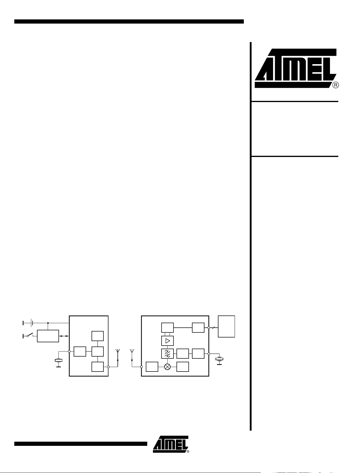
Figure 1-1. System Block Diagram
UHF ASK/FSK
Remote control receiver
Demod Control
PLL XTO
1 to 3
Micro-
controller
1 Li cell
Keys
Encoder
ATARx9x
UHF ASK/FSK
Remote control transmitter
ATA8403 ATA5760/
PLL
XTO
Antenna
VCO
ATA5761
Antenna
ATA8403
LNA
LNA VCO
4983A–IND–02/07
Page 2
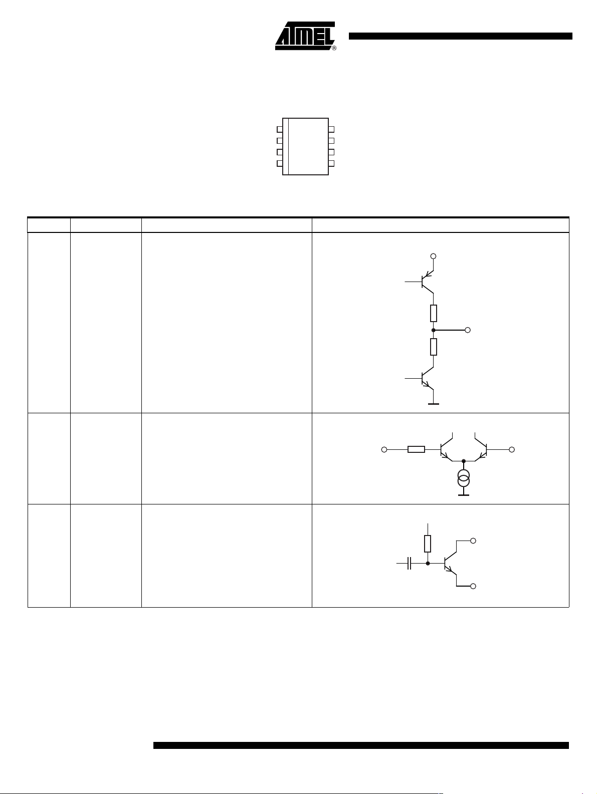
2. Pin Configuration
Figure 2-1. Pinning TSSOP8L
CLK
PA_ENABLE
ANT2
ANT1
1
8
ENABLE
2
3
4
GND
7
VS
6
XTAL
5
Table 2-1. Pin Description
Pin Symbol Function Configuration
Clock output signal for microconroller
1CLK
The clock output frequency is set by the
crystal to f
XTAL
/4
100Ω
100Ω
VS
CLK
2 PA_ENABLE
3
4
ANT2
ANT1
Switches on power amplifier, which is
used for ASK modulation
Emitter of antenna output stage
Open collector antenna output
50 kΩ
20 µA
ANT1
ANT2
U
= 1.1V PA_ENABLE
REF
2
ATA8403
4983A–IND–02/07
Page 3
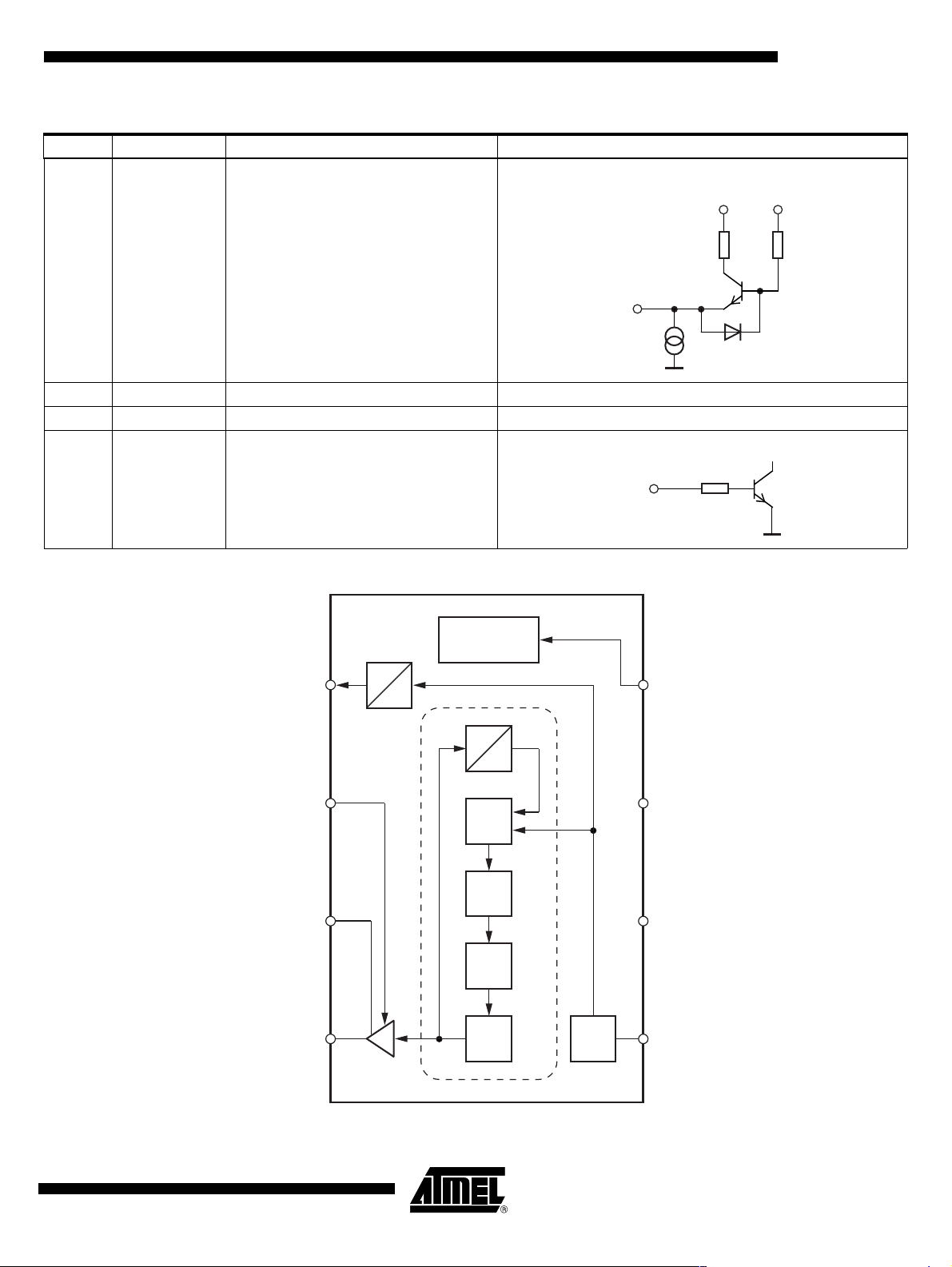
Table 2-1. Pin Description (Continued)
Pin Symbol Function Configuration
ATA8403
VS
1.5 kΩ 1.2 kΩ
VS
5 XTAL Connection for crystal
XTAL
182 µA
6 VS Supply voltage See ESD protection circuitry (see Figure 4-5 on page 9)
7 GND Ground See ESD protection circuitry (see Figure 4-5 on page 9)
ENABLE
200 kΩ
8 ENABLE Enable input
Figure 2-2. Block Diagram
ATA8403
Power up/down
CLK
PA_ENABLE
ANT2
ANT1
f
1
2
3
4
4
PA VCO
PLL
f
PDF
CP
LF
64
XTO
8
7
6
5
ENABLE
GND
VS
XTAL
4983A–IND–02/07
3
Page 4

3. General Description
This fully integrated PLL transmitter allows particularly simple, low-cost RF miniature transmitters to be assembled. The VCO is locked to 64 × f
needed for a 868.3 MHz transmitter and a 14.2969 MHz crystal for a 915 MHz transmitter. All
other PLL and VCO peripheral elements are integrated.
The XTO is a series resonance oscillator so that only one capacitor together with a crystal connected in series to GND are needed as external elements.
The crystal oscillator together with the PLL typically needs < 1 ms until the PLL is locked and the
CLK output is stable. There is a wait time of ≥ 4 ms must be used until the CLK is used for the
microcontroller and the PA is switched on.
The power amplifier is an open-collector output delivering a current pulse, which is nearly independent from the load impedance. The delivered output power is therefore controllable via the
connected load impedance.
This output configuration enables a simple matching to any kind of antenna or to 50Ω. A high
power efficiency of η=P
an optimized load impedance of Z
4. Functional Description
If ENABLE = L and the PA_ENABLE = L, the circuit is in standby mode, consuming only a very
small amount of current, so that a lithium cell used as power supply can work for several years.
out
, and therefore a 13.5672 MHz crystal is
XTAL
/(I
× VS) of 24% for the power amplifier at 868.3 MHz results when
S,PA
= (166 + j226)Ω is used at 3V supply voltage.
Load
With ENABLE = H the XTO, PLL, and the CLK driver are switched on. If PA_ENABLE remains
L, only the PLL and the XTO are running and the CLK signal is delivered to the microcontroller.
The VCO locks to 64 times the XTO frequency.
With ENABLE = H and PA_ENABLE = H the PLL, XTO, CLK driver, and the power amplifier are
on. The power amplifier can be switched on and off with PA_ENABLE. This is used to perform
the ASK modulation.
4.1 ASK Transmission
The ATA8403 is activated by ENABLE = H. PA_ENABLE must remain L for t ≥ 4 ms, then the
CLK signal can be taken to clock the microcontroller, and the output power can be modulated by
means of the PA_ENABLE pin. After transmission, PA_ENABLE is switched to L, and the microcontroller switches back to internal clocking. The ATA8403 is switched back to standby mode
with ENABLE = L.
4.2 FSK Transmission
The ATA8403 is activated by ENABLE = H. PA_ENABLE must remain L for t ≥ 4 ms, then the
CLK signal can be taken to clock the microcontroller and the power amplifier is switched on with
PA_ENABLE = H. The chip is then ready for FSK modulation. The microcontroller starts to
switch on and off the capacitor between the XTAL load capacitor and GND with an open-drain
output port, thus changing the reference frequency of the PLL. If the switch is closed, the output
frequency is lower than if the switch is open. After transmission PA_ENABLE is switched to L
and the microcontroller switches back to internal clocking. The ATA8403 is switched back to
standby mode with ENABLE = L.
The accuracy of the frequency deviation with XTAL pulling method is about ±25% when the following tolerances are considered.
4
ATA8403
4983A–IND–02/07
Page 5

Figure 4-1. Tolerances of Frequency Modulation
V
S
XTAL
C
Stray1
L
M
C
M
ATA8403
C
Stray2
R
S
C
4
Using C
=9.2pF±2%, C5= 6.8 pF ±5%, a switch port with C
4
tances on each side of the crystal of C
crystal of C
= 3.2 pF ±10% and a crystal with CM= 13 fF ±10%, typically results in an FSK devi-
0
ation of ±21.5 kHz with worst case tolerances of ±16.8 kHz to ±28.0 kHz.
4.3 CLK Output
An output CLK signal is provided for a connected microcontroller. The delivered signal is CMOS
compatible if the load capacitance is lower than 10 pF.
4.3.1 Clock Pulse Take-over
The clock of the crystal oscillator can be used for clocking the microcontroller. A special feature
of Atmel
with ENABLE = H, and after 4 ms assumes the clock signal of the transmission IC, so that the
message can be sent with crystal accuracy.
4.3.2 Output Matching and Power Setting
The output power is set by the load impedance of the antenna. The maximum output power is
achieved with a load impedance of Z
resistive path to V
The delivered current pulse of the power amplifier is 7.7 mA. The maximum output power is
delivered to a resistive load of 475Ω if the 0.53 pF output capacitance of the power amplifier is
compensated by the load impedance.
®
’s ATARx9x is that it starts with an integrated RC-oscillator to switch on the ATA8403
to deliver the DC current.
S
C
0
Stray1=CStray2
= (166 + j226)Ω at 868.3 MHz. There must be a low
Load,opt
= 1 pF ±10%, a parallel capacitance of the
C
5
C
Switch
= 3 pF ±10%, stray capaci-
Switch
4983A–IND–02/07
An optimum load impedance of:
Z
=475Ω|| j/(2 × p × f × 0.53 pF) = (166 + j226)Ω thus results in the maximum output power
Load
of 5.5 dBm.
The load impedance is defined as the impedance seen from the ATA8403’s ANT1, ANT2 into
the matching network. Do not confuse this large signal load impedance with a small signal input
impedance delivered as input characteristic of RF amplifiers and measured from the application
into the IC instead of from the IC into the application for a power amplifier.
Less output power is achieved by lowering the real parallel part of 475Ω where the parallel imag-
inary part should be kept constant.
Output power measurement can be done with the circuit shown in Figure 4-2 on page 6. Note
that the component values must be changed to compensate for the individual board parasitics
until the ATA8403 has the right load impedance Z
= (166 + j226)Ω at 868.3 MHz. Also the
Load,opt
damping of the cable used to measure the output power must be calibrated out.
5
Page 6

Figure 4-2. Output Power Measurement
4.4 Application Circuit
A value of 68 nF/X7R is recommended for the supply-voltage blocking capacitor C3 (see Figure
4-3 on page 7 and Figure 4-4 on page 8). C
power amplifier where C
series should be used to achieve a better tolerance value and to have the possibility of realizing
the Z
C
, together with the pins of ATA8403 and the PCB board wires, forms a series resonance loop
1
that suppresses the 1
mally the best suppression is achieved when C
and ANT2.
ANT1
Z
ANT2
typically is 3.9 pF/NP0 and C2 is 1 pF/NP0. For C2, two capacitors in
1
using standard valued capacitors.
Load,opt
st
harmonic. Therefore, the position of C1 on the PCB is important. Nor-
V
Lopt
S
C
1
1 nF
10 nH
L
1
C
2
1.5 pF
C
3
and C2 are used to match the loop antenna to the
1
Z = 50Ω
2.7 pF
is placed as close as possible to the pins ANT1
1
Power
meter
R
50Ω
in
The loop antenna should not exceed a width of 1.5 mm, otherwise the Q-factor of the loop
antenna is too high.
L
(≈ 50 nH to 100 nH) can be printed on PCB. C4 should be selected so that the XTO runs on
1
the load resonance frequency of the crystal. Normally, a 15 pF load-capacitance crystal results
in a value of 12 pF.
6
ATA8403
4983A–IND–02/07
Page 7

Figure 4-3. ASK Application Circuit
ATA8403
S1
BPXY
S2
BPXY
BPXY
OSC1
CLK
PA_ENABLE
ATARx9x
7
ATA8403
1
VDD
1
VSS
20
BPXY
Power up/down
f
4
f
64
ENABLE
8
GND
VS
Loop
Antenna
C2
L1
C1
VS
ANT2
ANT1
2
3
PA VCO
4
PLL
PDF
CP
LF
XTO
7
C3
VS
6
VS
XTAL XTAL
5
C4
4983A–IND–02/07
7
Page 8
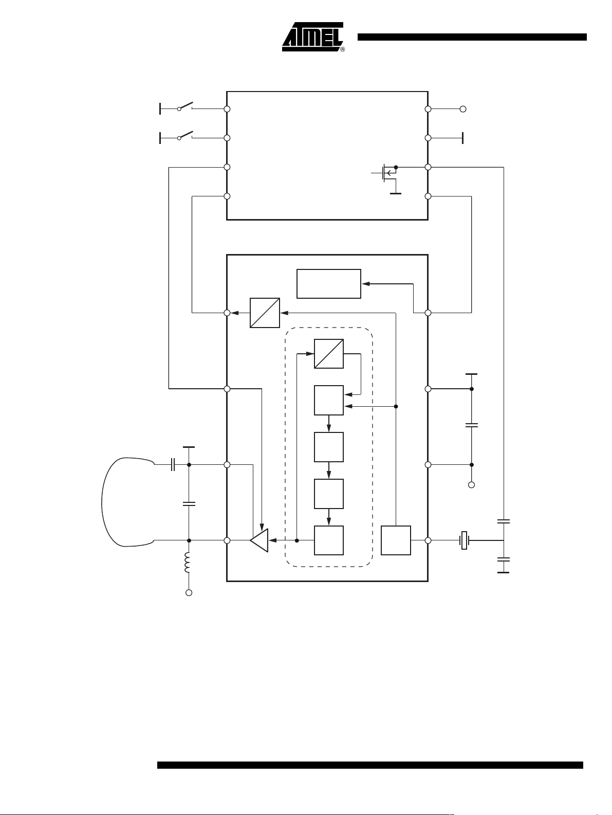
Figure 4-4. FSK Application Circuit
S1
BPXY
S2
BPXY
BPXY
OSC1
CLK
PA_ENABLE
ATARx9x
7
ATA8403
1
VDD
1
VSS
20
BP42/T2O
18
BPXY
Power up/down
f
4
f
64
ENABLE
8
GND
VS
Loop
Antenna
C2
C1
L1
VS
ANT2
ANT1
2
3
PA VCO
4
PLL
PDF
CP
LF
XTO
7
C3
VS
6
VS
C5
XTAL XTAL
5
C4
8
ATA8403
4983A–IND–02/07
Page 9

Figure 4-5. ESD Protection Circuit
VS
ATA8403
ANT1
CLK
GND
PA_ENABLE XTALANT2 ENABLE
5. Absolute Maximum Ratings
Stresses beyond those listed under “Absolute Maximum Ratings” may cause permanent damage to the device. This is a stress rating
only and functional operation of the device at these or any other conditions beyond those indicated in the operational sections of this
specification is not implied. Exposure to absolute maximum rating conditions for extended periods may affect device reliability.
Parameters Symbol Minimum Maximum Unit
Supply voltage V
Power dissipation P
Junction temperature T
Storage temperature T
Ambient temperature T
Input voltage V
Note: 1. If V
+ 0.3 is higher than 3.7V, the maximum voltage will be reduced to 3.7V.
S
maxPA_ENABLE
S
tot
stg
amb
j
–55 +85 °C
–55 +85 °C
–0.3 (VS + 0.3)
5V
100 mW
150 °C
(1)
V
6. Thermal Resistance
Parameters Symbol Value Unit
Junction ambient R
thJA
170 K/W
7. Electrical Characteristics
VS = 2.0V to 4.0V, T
Typical values are given at V
Parameters Test Conditions Symbol Min. Typ. Max. Unit
Supply current
Supply current
Output power
Note: 1. If V
= 25°C unless otherwise specified.
amb
= 3.0V and T
S
= 25°C. All parameters are referred to GND (pin 7).
amb
Power down,
V
V
< 0.25V, –40°C to 85°C
ENABLE
PA_ENABLE
< 0.25V, 25°C
(100% correlation tested)
Power up, PA off, V
V
Power up, V
V
VS= 3.0V, T
ENABLE
ENABLE
>1.7V, V
S
>1.7V, V
amb
f = 868.3 MHz, Z
is higher than 3.6V, the maximum voltage will be reduced to 3.6V.
S
= 3V,
S
PA_ENABLE
= 3.0,
PA_ENABLE
=25°C,
= (166 + j226)Ω
Load
<0.25V
>1.7V
I
S_Off
I
S
I
S_Transmit
P
Ref
350 nA
< 10
nA
3.6 4.6 mA
8.5 11 mA
3.5 5.5 8 dBm
4983A–IND–02/07
9
Page 10
7. Electrical Characteristics (Continued)
VS = 2.0V to 4.0V, T
Typical values are given at VS = 3.0V and T
Parameters Test Conditions Symbol Min. Typ. Max. Unit
Output power variation for the full
temperature range
Output power variation for the full
temperature range
Achievable output-power range Selectable by load impedance P
Spurious emission
Oscillator frequency XTO
(= phase comparator frequency)
PLL loop bandwidth 250 kHz
Phase noise of phase comparator
In-loop phase noise PLL 25 kHz distance to carrier –80 –74 dBc/Hz
Phase noise VCO
Frequency range of VCO f
Clock output frequency (CMOS
microcontroller compatible)
Voltage swing at pin CLK C
Series resonance R of the crystal Rs 110 Ω
Capacitive load at pin XT0 7pF
FSK modulation frequency rate Duty cycle of the modulation signal = 50% 0 32 kHz
ASK modulation frequency rate Duty cycle of the modulation signal = 50% 0 50 kHz
ENABLE input
PA_ENABLE input
Note: 1. If VS is higher than 3.6V, the maximum voltage will be reduced to 3.6V.
= 25°C unless otherwise specified.
amb
T
amb
= 25°C. All parameters are referred to GND (pin 7).
amb
= 25°C,
VS = 3.0V
= 2.0V
V
S
= 25°C,
T
amb
VS = 3.0V
VS = 2.0V,
= P
P
f
Out
CLK
Ref
= f0/128
+ ∆P
Load capacitance at pin CLK = 10 pF
f
±1 × f
O
±4 × f
f
O
CLK
CLK
Other spurious are lower
= f0/32
f
XTO
f
= resonant frequency of the XTAL,
XTAL
≤ 10 fF, load capacitance selected
C
M
accordingly
T
= 25°C
amb
Referred to f
PC
25 kHz distance to carrier
At 1 MHz
At 36 MHz
≤ 10 pF
Load
Low level input voltage
High level input voltage
Input current high
Low level input voltage
High level input voltage
Input current high
= f
Ref
XT0,
∆P
Ref
∆P
Ref
∆P
Ref
∆P
Ref
Out_typ
f
XTO
VCO
V
0h
V
0l
V
V
Ih
I
In
V
V
Ih
I
In
–1.5
–4.0
–2.0
–4.5
dB
dB
dB
dB
–3 +5.5 dBm
–52
–52
f
XTAL
dBc
dBc
ppm
–116 –110 dBc/Hz
–89
–120
–86
–117
dBc/Hz
dBc/Hz
868 928 MHz
/256 MHz
f
0
VS× 0.8
× 0.2
V
S
Il
0.25
1.7
20
Il
1.7
0.25
V
S
(1)
5
V
V
V
V
µA
V
V
µA
10
ATA8403
4983A–IND–02/07
Page 11
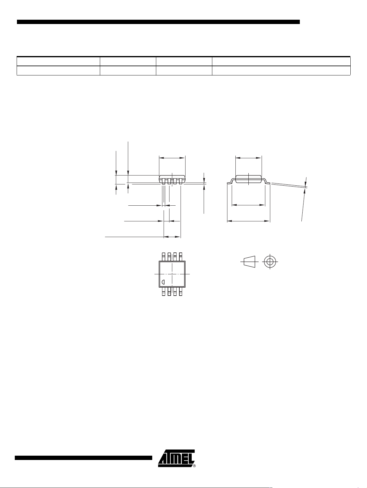
8. Ordering Information
Extended Type Number Package MOQ Remarks
ATA8403-6AQY TSSOP8L 5000 pcs Taped and reeled, Pb-free
9. Package Information
Package: TSSOP 8L
Dimensions in mm
ATA8403
+0.05
0.85±0.05
1-0.15
0.31
0.65 nom.
3 x 0.65 = 1.95 nom.
Drawing-No.: 6.543-5083.01-4
Issue: 2; 15.03.04
+0.06
-0.07
3±0.1
85
14
0.1±0.05
3±0.1
3.8±0.3
4.9±0.1
technical drawings
according to DIN
specifications
-0.02
+0.05
0.15
4983A–IND–02/07
11
Page 12

Atmel Corporation Atmel Operations
2325 Orchard Parkway
San Jose, CA 95131, USA
Tel: 1(408) 441-0311
Fax: 1(408) 487-2600
Regional Headquarters
Europe
Atmel Sarl
Route des Arsenaux 41
Case Postale 80
CH-1705 Fribourg
Switzerland
Tel: (41) 26-426-5555
Fax: (41) 26-426-5500
Asia
Room 1219
Chinachem Golden Plaza
77 Mody Road Tsimshatsui
East Kowloon
Hong Kong
Tel: (852) 2721-9778
Fax: (852) 2722-1369
Japan
9F, Tonetsu Shinkawa Bldg.
1-24-8 Shinkawa
Chuo-ku, Tokyo 104-0033
Japan
Tel: (81) 3-3523-3551
Fax: (81) 3-3523-7581
Memory
2325 Orchard Parkway
San Jose, CA 95131, USA
Tel: 1(408) 441-0311
Fax: 1(408) 436-4314
Microcontrollers
2325 Orchard Parkway
San Jose, CA 95131, USA
Tel: 1(408) 441-0311
Fax: 1(408) 436-4314
La Chantrerie
BP 70602
44306 Nantes Cedex 3, France
Tel: (33) 2-40-18-18-18
Fax: (33) 2-40-18-19-60
ASIC/ASSP/Smart Cards
Zone Industrielle
13106 Rousset Cedex, France
Tel: (33) 4-42-53-60-00
Fax: (33) 4-42-53-60-01
1150 East Cheyenne Mtn. Blvd.
Colorado Springs, CO 80906, USA
Tel: 1(719) 576-3300
Fax: 1(719) 540-1759
Scottish Enterprise Technology Park
Maxwell Building
East Kilbride G75 0QR, Scotland
Tel: (44) 1355-803-000
Fax: (44) 1355-242-743
RF/Automotive
Theresienstrasse 2
Postfach 3535
74025 Heilbronn, Germany
Tel: (49) 71-31-67-0
Fax: (49) 71-31-67-2340
1150 East Cheyenne Mtn. Blvd.
Colorado Springs, CO 80906, USA
Tel: 1(719) 576-3300
Fax: 1(719) 540-1759
Biometrics
Avenue de Rochepleine
BP 123
38521 Saint-Egreve Cedex, France
Tel: (33) 4-76-58-47-50
Fax: (33) 4-76-58-47-60
Literature Requests
www.atmel.com/literature
Disclaimer: The information in this document is provided in connection with Atmel products. No license, express or implied, by estoppel or otherwise, to any
intellectual property right is granted by this document or in connection with the sale of Atmel products. EXCEPT AS SET FORTH IN ATMEL’S TERMS AND CONDI-
TIONS OF SALE LOCATED ON ATMEL’S WEB SITE, ATMEL ASSUMES NO LIABILITY WHATSOEVER AND DISCLAIMS ANY EXPRESS, IMPLIED OR STATUTORY
WARRANTY RELATING TO ITS PRODUCTS INCLUDING, BUT NOT LIMITED TO, THE IMPLIED WARRANTY OF MERCHANTABILITY, FITNESS FOR A PARTICULAR
PURPOSE, OR NON-INFRINGEMENT. IN NO EVENT SHALL ATMEL BE LIABLE FOR ANY DIRECT, INDIRECT, CONSEQUENTIAL, PUNITIVE, SPECIAL OR INCIDENTAL DAMAGES (INCLUDING, WITHOUT LIMITATION, DAMAGES FOR LOSS OF PROFITS, BUSINESS INTERRUPTION, OR LOSS OF INFORMATION) ARISING OUT
OF THE USE OR INABILITY TO USE THIS DOCUMENT, EVEN IF ATMEL HAS BEEN ADVISED OF THE POSSIBILITY OF SUCH DAMAGES. Atmel makes no
representations or warranties with respect to the accuracy or completeness of the contents of this document and reserves the right to make changes to specifications
and product descriptions at any time without notice. Atmel does not make any commitment to update the information contained herein. Unless specifically provided
otherwise, Atmel products are not suitable for, and shall not be used in, automotive applications. Atmel’s products are not intended, authorized, or warranted for use
as components in applications intended to support or sustain life.
© 2007 Atmel Corporation. All rights reserved. Atmel®, logo and combinations thereof, Everywhere You Are® and others are registered trade-
marks or trademarks of Atmel Corporation or its subsidiaries. Other terms and product names may be trademarks of others.
4983A–IND–02/07
 Loading...