

Page 1

Features
• Six Half-bridge Outputs Formed by Six High-side and Six Low-side Drivers
• Capable of Switching all Kinds of Loads (Such as DC Motors, Bulbs, Resistors,
Capacitors and Inductors)
• R
• Up to 650-mA Output Current
• Very Low Quiescent Current I
• Outputs Short-circuit Protected
• Overtemperature Prewarning and Protection
• Undervoltage Protection
• Various Diagnosis Functions Such as Shorted Output, Open Load, Overtemperature
• Serial Data Interface
• Operation Voltage up to 40V
• Daisy Chaining Possible
• Serial Interface 5V and 3.3V Compatible, up to 2 MHz Clock Frequency
• QFN24 Package
Typically 1.0Ω at 25°C, Maximum 2.2Ω at 200°C
DSon
< 20 µA in Standby Mode
S
and Power Supply Fail
High
Temperature
Hex Half-bridge
Driver with
Serial Input
1. Description
The ATA6837 is designed for high-temperature applications. In mechatronic solutions,
for example, turbo charger or exhaust gas recirculation systems, many flaps have to
be controlled by DC motor driver ICs which are located very close to the hot engine or
actuator and where ambient temperatures up to 150°C are usual. Due to the advantages of SOI technology, junction temperatures up to 200°C are allowed. This enables
new cost-effective board design possibilities to achieve complex mechatronic
solutions.
The ATA6837 is a fully protected hex half-bridge driver, used to control up to 6 different loads by a microcontroller in automotive and industrial applications.
Each of the six high-side and six low-side drivers is capable of driving currents up to
650 mA. The drivers are internally connected to form 6 half-bridges and can be controlled separately from a standard serial data interface. Therefore, all kinds of loads,
such as bulbs, resistors, capacitors and inductors, can be combined. The IC especially supports the application of H-bridges to drive DC motors.
Protection is guaranteed in terms of short-circuit conditions, overtemperature and
undervoltage. Various diagnosis functions and a very low quiescent current in standby
mode make a wide range of applications possible.
Automotive qualification referring to conducted interferences, EMC protection and
ESD protection gives added value and enhanced quality for the exacting requirements
of automotive applications.
Control
ATA6837
Preliminary
4953C–AUTO–09/07
Page 2
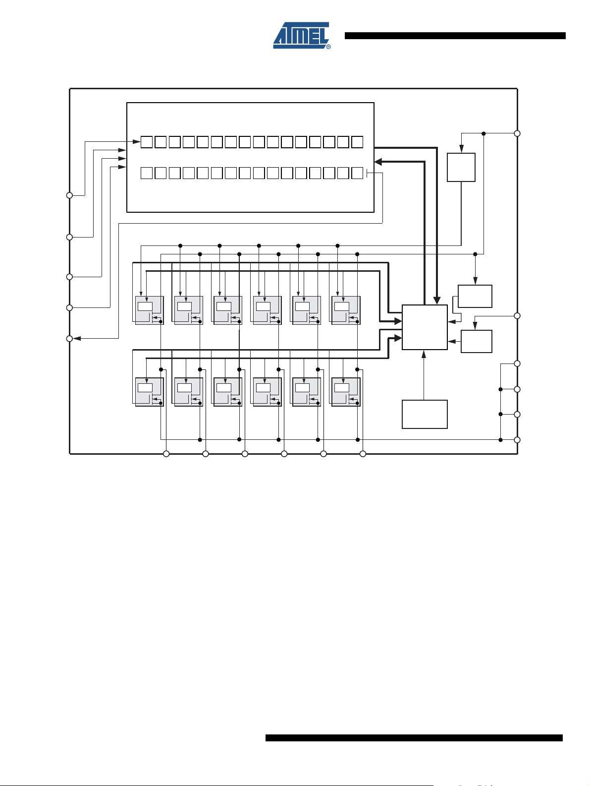
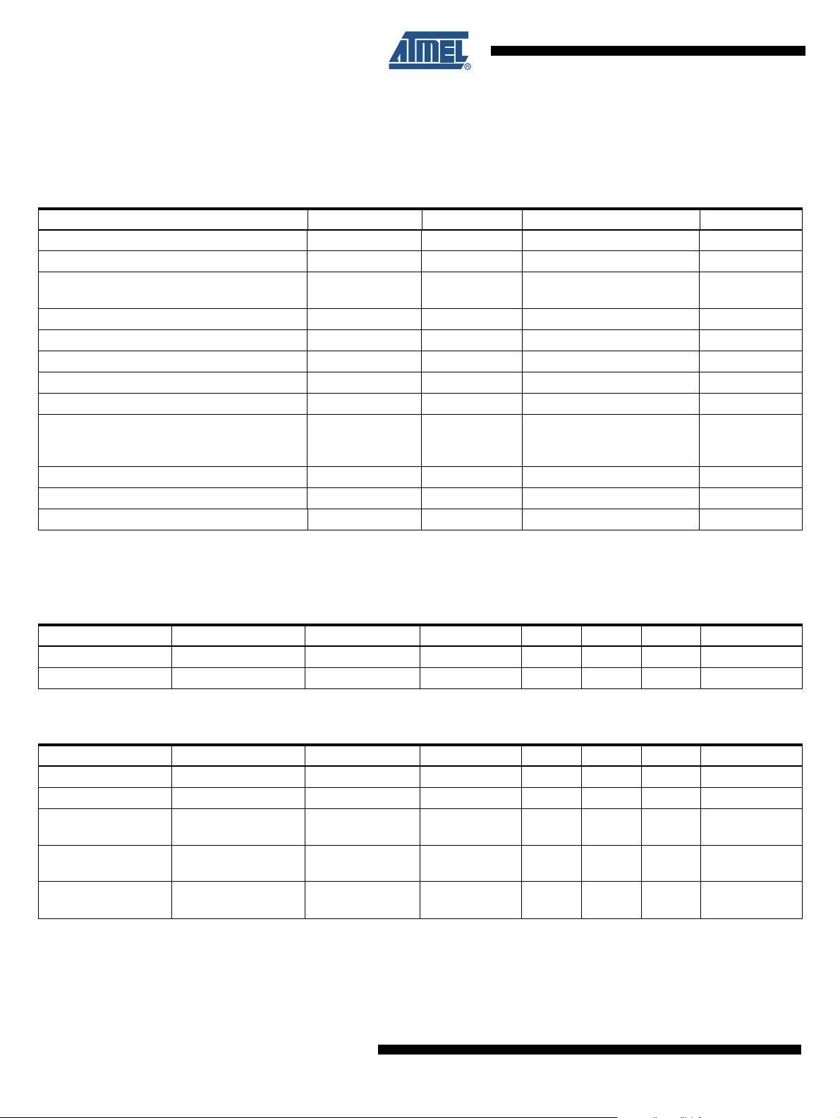
Figure 1-1. Block Diagram QFN24
O
S
L
S
C
D
I
T
Input register
Ouput register
P
I
S
S
N
C
F
H
D
Fault
Detect
Fault
Detect
11
OUT1
CLK
CS
INH
DO
DI
19
18
17
Fault
Detect
12
13
Fault
Detect
H
L
H
L
H
H
L
H
L
S
S
6
6
H
S
S
S
5
5
4
L
L
S
4
S
S
3
S
S
2
2
3
S
S
S
R
1
1
R
Serial interface
H
H
L
S
S
6
6
823
OUT2
H
S
5
Fault
Detect
Fault
Detect
L
S
5
H
S
4
5
OUT3
L
L
S
4
Fault
Detect
Fault
Detect
H
L
S
2
Fault
Detect
Fault
Detect
H
S
S
2
1
S
S
3
3
2
OUT4 OUT5 OUT6
Fault
Detect
Fault
Detect
T
L
P
S
1
20
Control
logic
Thermal
protection
3, 4
VS
Charge
pump
UV
protection
14
VCC
Power on
reset
24
GND
16
GND
15
GND
7
GND
2
ATA6837 [Preliminary]
4953C–AUTO–09/07
Page 3
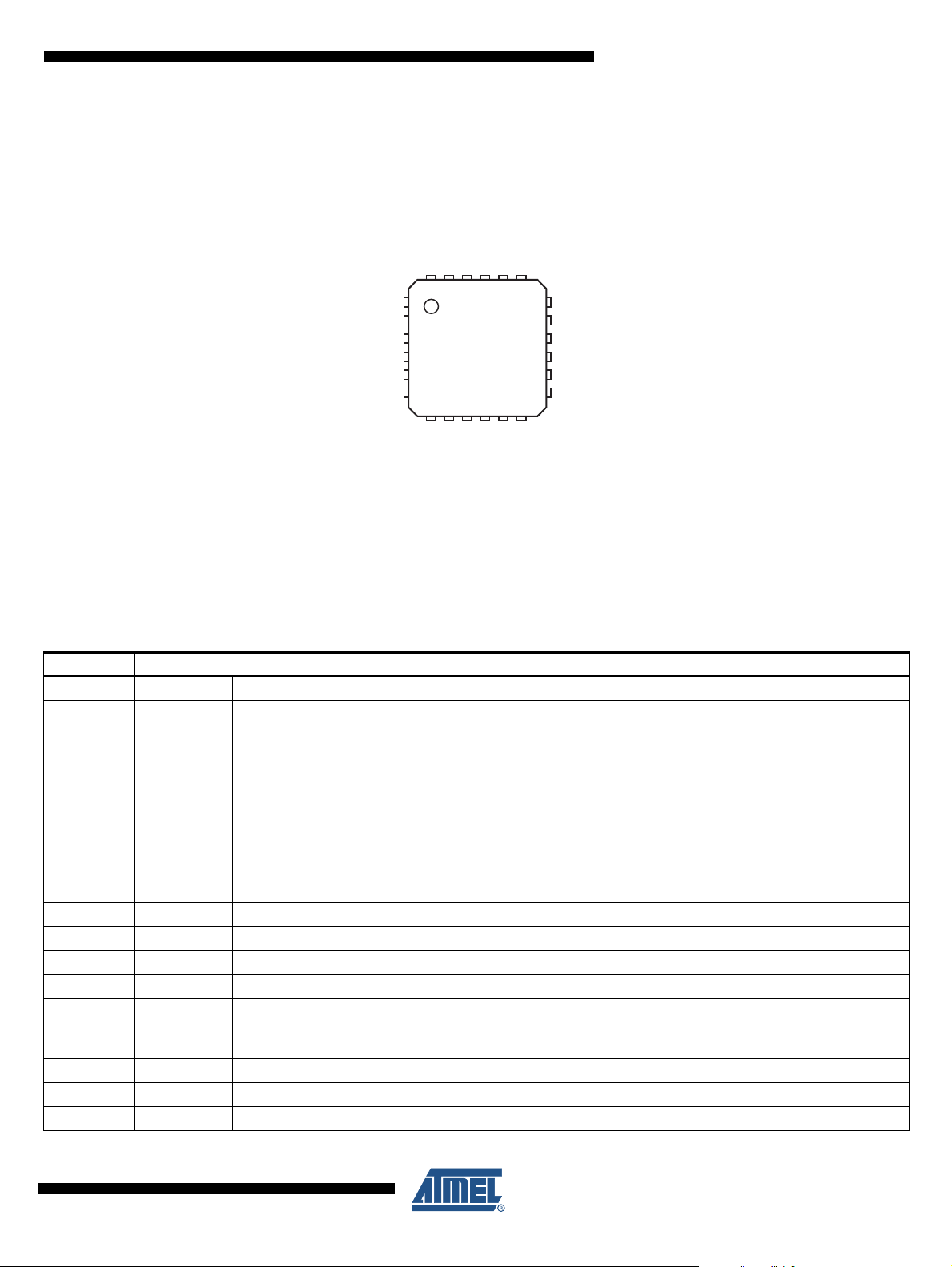
2. Pin Configuration
Figure 2-1. Pinning QFN 24, 5 × 5, 0.65 mm pitch
OUT4 SENSE
OUT4
VS
VS
OUT3
OUT3 SENSE
NC
OUT5
OUT5 SENSE
24 23 22 21 1920
1
2
3
4
5
6
78910 1211
OUT6 SENSE
OUT6
DI
CLK
18
17
CS
16
GND SENSE
NC
15
14
VCC
13
DO
ATA6837 [Preliminary]
NC
OUT2
OUT2 SENSE
INH
OUT1
OUT1 SENSE
Note: YWW Date code (Y = Year above 2000, WW = week number)
ATAxyz Product name
ZZZZZ Wafer lot number
AL Assembly sub-lot number
Table 2-1. Pin Description QFN24
Pin Symbol Function
1 OUT4 SENSE Only for testability in final test
Half-bridge output 4; formed by internally connected power MOS high-side switch 4 and low-side switch 4
2OUT4
3 VS Power supply output stages HS4, HS5 and HS6
4 VS Power supply output stages HS1, HS2 and HS3
5 OUT3 Output 3; see pin 1
6 OUT3 SENSE Only for testability in final test
7 NC Internal bond to GND
8 OUT2 Output 2; see pin 1
9 OUT2 SENSE Only for testability in final test
10 OUT1 SENSE Only for testability in final test
11 OUT1 Output 1; see pin 1
12 INH Inhibit input; 5V/3.3V logic input with internal pull down; low = standby, high = normal operation
13 DO
14 VCC Logic supply voltage (5V/3.3V)
15 NC Internal bond to GND
16 GND SENSE Ground; reference potential; internal connection to the lead frame; cooling tab
with internal reverse diodes; short circuit protection; overtemperature protection; diagnosis for short and
open load
Serial data output; 5V/3.3V CMOS logic level tri-state output for output (status) register data; sends 16-bit
status information to the microcontroller (LSB is transferred first). Output will remain tri-stated unless
device is selected by CS = low, therefore, several ICs can operate on one data output line only
4953C–AUTO–09/07
3
Page 4
Table 2-1. Pin Description QFN24 (Continued)
Pin Symbol Function
17 CS
18 CLK
19 DI
20 OUT6 Output 6; see pin 1
21 OUT6 SENSE Only for testability in final test
22 OUT5 SENSE Only for testability in final test
23 OUT5 Output 5; see pin 1
24 NC Internal bond to GND
Chip select input; 5V/3.3V CMOS logic level input with internal pull up;
low = serial communication is enabled, high = disabled
Serial clock input; 5V/3.3V CMOS logic level input with internal pull down;
controls serial data input interface and internal shift register (f
Serial data input; 5V/3.3V CMOS logic level input with internal pull down; receives serial data from the
control device; DI expects a 16-bit control word with LSB being transferred first
= 2 MHz)
max
4
ATA6837 [Preliminary]
4953C–AUTO–09/07
Page 5
3. Functional Description
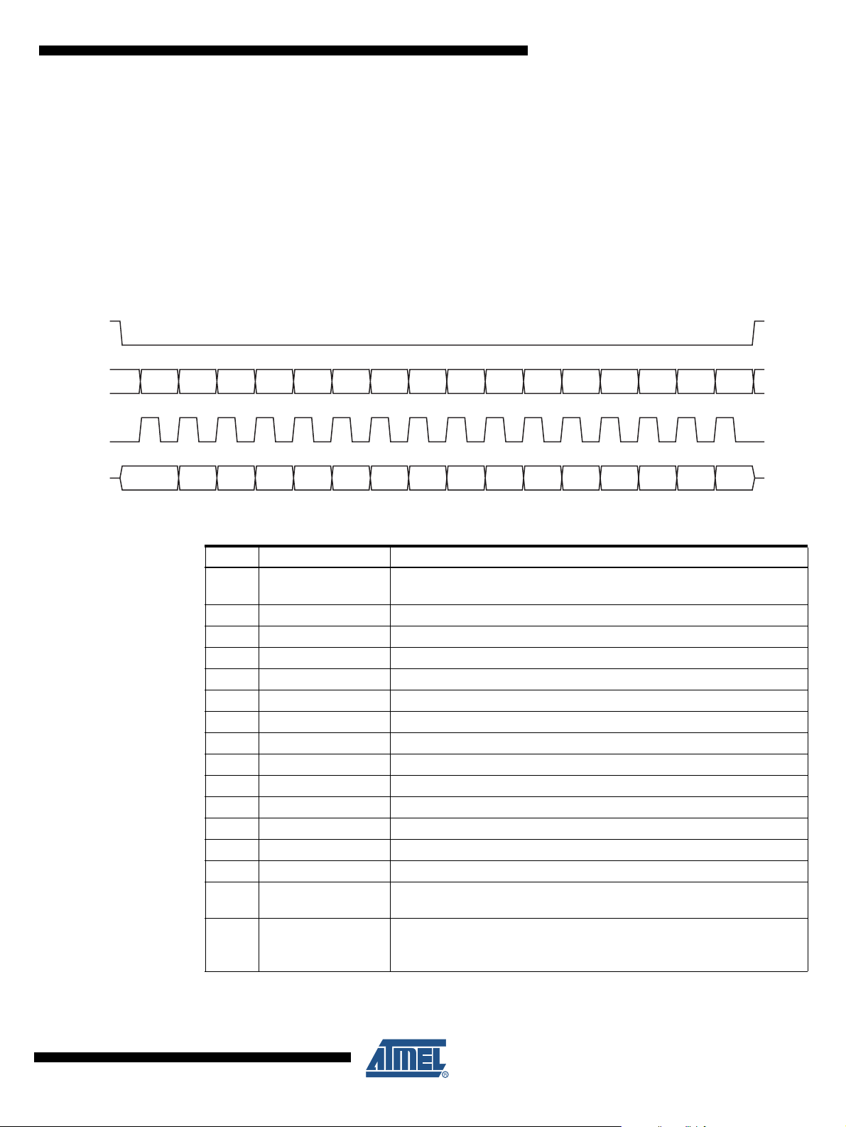
3.1 Serial Interface
Data transfer starts with the falling edge of the CS signal. Data must appear at DI synchronized
to CLK and is accepted on the falling edge of the CLK signal. LSB (bit 0, SRR) has to be transferred first. Execution of new input data is enabled on the rising edge of the CS signal. When CS
is high, pin DO is in a tri-state condition. This output is enabled on the falling edge of CS. Output
data will change their state with the rising edge of CLK and stay stable until the next rising edge
of CLK appears. LSB (bit 0, TP) is transferred first.
Figure 3-1. Data Transfer Input Data Protocol
CS
ATA6837 [Preliminary]
CLK
DO
DI
SRR LS1 HS1 LS2 HS2 LS3
0 1 2 3 4 5 6 7 8 9 10 11 12 13 14 15
TP SLS1 SHS1 SLS2 SHS2 SLS3 SHS3 SLS4
HS3
LS4
HS4 LS5 HS5 LS6 HS6
SHS4 SLS5 SHS5 SLS6 SHS6 SCD INH PSF
OLD
SCT SI
Table 3-1. Input Data Protocol
Bit Input Register Function
0SRR
1 LS1 Controls output LS1 (high = switch output LS1 on)
2 HS1 Controls output HS1 (high = switch output HS1 on)
3 LS2 See LS1
4 HS2 See HS1
5 LS3 See LS1
6 HS3 See HS1
7 LS4 See LS1
8 HS4 See HS1
9 LS5 See LS1
10 HS5 See HS1
11 LS6 See LS1
12 HS6 See HS1
13 OLD Open load detection (low = on)
14 SCT
15 SI
Status register reset (high = reset; the bits PSF, SCD and
overtemperature shutdown in the output data register are set to low)
Programmable time delay for short circuit
(shutdown delay high/low = 12 ms/1.5 ms)
Software inhibit; low = standby, high = normal operation
(data transfer is not affected by standby function because the digital
part is still powered)
4953C–AUTO–09/07
5
Page 6
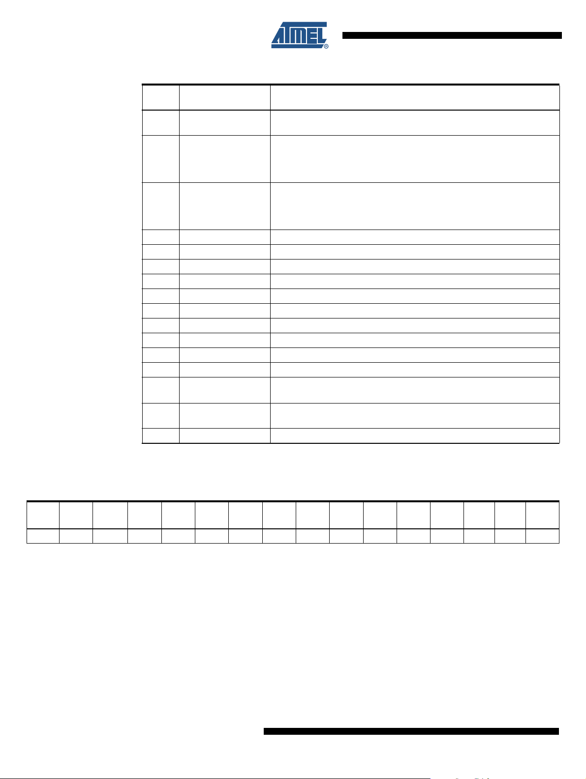
Table 3-2. Output Data Protocol
Output (Status)
Bit
0TP
1 Status LS1
2 Status HS1
3 Status LS2 Description see LS1
4 Status HS2 Description see HS1
5 Status LS3 Description see LS1
6 Status HS3 Description see HS1
7 Status LS4 Description see LS1
8 Status HS4 Description see HS1
9 Status LS5 Description see LS1
10 Status HS5 Description see HS1
11 Status LS6 Description see LS1
12 Status HS6 Description see HS1
13 SCD
14 INH
15 PSF Power supply fail: undervoltage at pin VS detected
Note: Bit 0 to 15 = high: overtemperature shutdown
Register Function
Temperature prewarning: high = warning
(overtemperature shutdown see remark below)
Normal operation: high = output is on, low = output is off
Open-load detection: high = open load, low = no open load
(correct load condition is detected if the corresponding output is
switched off)
Normal operation: high = output is on, low = output is off
Open-load detection: high = open load, low = no open load
(correct load condition is detected if the corresponding output is
switched off)
Short circuit detected: set high, when at least one output is switched off
by a short circuit condition
Inhibit: this bit is controlled by software (bit SI in input register) and
hardware inhibit (pin INH). High = standby, low = normal operation
Table 3-3. Status of the Input Register After Power on Reset
Bit 15
6
Bit 14
(SI)
(SCT)
HHHLLLLLLLLLLLLL
Bit 13
(OLD)
Bit 12
(HS6)
Bit 11
(LS6)
Bit 10
(HS5)
Bit 9
(LS5)
Bit 8
(HS4)
Bit 7
(LS4)
Bit 6
(HS3)
Bit 5
(LS3)
Bit 4
(HS2)
Bit 3
(LS2)
Bit 2
(HS1)
Bit 1
(LS1)
Bit 0
(SRR)
ATA6837 [Preliminary]
4953C–AUTO–09/07
Page 7

3.2 Power-supply Fail
In case of undervoltage at pin VS, an internal timer is started. When during a permanent undervoltage the delay time (t
set and all outputs are disabled. When normal voltage is present again, the outputs are enabled
immediately. The PSF bit remains high until it is reset by the SRR bit in the input register.
3.3 Open-load Detection
If the open-load detection bit (OLD) is set to low, a pull-up current for each high-side switch and
a pull-down current for each low-side switch is turned on (open-load detection current I
I
). If VVS–V
LS1-6
tion), the corresponding bit of the output in the output register is set to high. Switching on an
output stage with OLD bit set to low disables the open load function for this output.
3.4 Overtemperature Protection
If the junction temperature exceeds the thermal prewarning threshold, T
prewarning bit (TP) in the output register is set. When the temperature falls below the thermal
prewarning threshold, T
a complete 16-bit data word: with CS = high to low, the state of TP appears at pin DO. After the
microcontroller has read this information, CS is set high and the data transfer is interrupted without affecting the state of the input and output registers.
HS1-6
ATA6837 [Preliminary]
) is reached, the power supply fail bit (PSF) in the output register is
dUV
or V
is lower than the open-load detection threshold (open-load condi-
LS1-6
set, the temperature
jPW
reset, the bit TP is reset. The TP bit can be read without transferring
jPW
HS1-6
,
If the junction temperature exceeds the thermal shutdown threshold, T
disabled and all bits in the output register are set high. The outputs can be enabled again when
the temperature falls below the thermal shutdown threshold, T
been written to the SRR bit in the input register. Thermal prewarning and shutdown threshold
have hysteresis.
3.5 Short-circuit Protection
The output currents are limited by a current regulator. Current limitation takes place when the
overcurrent limitation and shutdown threshold (I
internal timer is started. The shorted output is disabled when during a permanent short the delay
time (t
) programmed by the short-circuit timer bit (SCT) is reached. Additionally, the short-cir-
dSd
cuit detection bit (SCD) is set. If the temperature prewarning bit TP in the output register is set
during a short, the shorted output is disabled immediately and SCD bit is set. By writing a high to
the SRR bit in the input register, the SCD bit is reset and the disabled outputs are enabled.
3.6 Inhibit
There are two ways to inhibit the ATA6837:
• Set bit SI in the input register to 0
• Switch pin INH to 0V
In both cases, all output stages are turned off but the serial interface stays active. The output
stages can be activated again by bit SI = 1 (when INH = VCC) or by pin INH switched back to
VCC (when SI = 1).
HS1-6
j switch off
j switch on
, I
) are reached. Simultaneously, an
LS1-6
, the outputs are
, and when a high has
4953C–AUTO–09/07
7
Page 8
4. Absolute Maximum Ratings
Stresses beyond those listed under “Absolute Maximum Ratings” may cause permanent damage to the device. This is a stress rating
only and functional operation of the device at these or any other conditions beyond those indicated in the operational sections of this
specification is not implied. Exposure to absolute maximum rating conditions for extended periods may affect device reliability.
All values refer to GND pins.
Parameters Pin Symbol Value Unit
Supply voltage V
Supply voltage t < 0.5s; I
Supply voltage difference
⏐ V
S_pin5–VS_pin10
>–2A V
S
⏐
∆V
Logic supply voltage V
Logic input voltage V
DI, VCLK, VCS
Logic output voltage V
Input current I
INH, IDI, ICLK, ICS
Output current I
Output current I
OUT1
Junction temperature range T
Storage temperature range T
Ambient temperature range
VS
VS
VCC
DO
DO
to I
STG
T
VS
OUT6
j
a
–0.3 to +40 V
–1 V
150 mV
–0.3 to +7 V
–0.3 to V
–0.3 to V
+0.3 V
VCC
+0.3 V
VCC
–10 to +10 mA
–10 to +10 mA
Internally limited, see
“Output Specification” in
Section 7. on page 9
–40 to +200 °C
–55 to +200 °C
–40 to +150 °C
5. Thermal Resistance
Table 5-1. QFN24: Depends on the PCB-board
Parameter Test Conditions Pin Symbol Min. Typ. Max. Unit
Junction pin R
Junction ambient R
thJP
thJA
< 5 K/W
35 K/W
6. Operating Range
Parameter Test Conditions Pin Symbol Min. Typ. Max. Unit
(1)
Supply voltage V
Logic supply voltage V
V
Logic input voltage
INH, VDI, VCLK,
Serial interface clock
frequency
Junction temperature
range
V
f
VS
VCC
CS
CLK
T
V
UV
35.5V
–0.3 V
j
–40 +200 °C
40 V
VCC
2MHz
V
8
ATA6837 [Preliminary]
4953C–AUTO–09/07
Page 9
ATA6837 [Preliminary]
7. Electrical Characteristics
7.5V < VS < 40V; 3V < VCC < 5.5V; INH = High; –40°C < Tj < 200°C, Ta≤ 150°C; unless otherwise specified, all values refer to GND pins.
No. Parameters Test Conditions
Pin
1 Current Consumption
< 28V,
V
1.1 Quiescent current (VS)
Quiescent current
1.2
(VCC)
VS
INH or bit SI = low
VCC
< 5.5V,
3V < V
INH or bit SI = low
VVS < 28V normal
1.3 Supply current (VS)
operation, all output
stages off
V
< 28V normal
1.4 Supply current (VS)
VS
operation, all output low
stages on, no load
< 28V normal
V
VS
1.5 Supply current (VS)
operation, all output
high stages on, no load
1.6 Supply current (VCC)
3V < V
normal operation
VCC
< 5.5V,
2 Internal Oscillator Frequency
Frequency (time base
2.1
for delay timers)
3 Undervoltage Detection, Power-on Reset
Power-on reset
3.1
threshold
Power-on reset delay
3.2
time
Undervoltage detection
3.3
threshold
Undervoltage detection
3.4
hysteresis
Undervoltage detection
3.5
delay
After switching on V
VCC
4 Thermal Prewarning and Shutdown
4.1 Thermal prewarning T
4.2 Thermal prewarning T
Thermal prewarning
4.3
hysteresis
4.4 Thermal shutdown T
4.5 Thermal shutdown T
Thermal shutdown
4.6
hysteresis
Ratio thermal
4.7
shutdown/thermal
prewarning
*) Type means: A = 100% tested, B = 100% correlation tested, C = Characterized on samples, D = Design parameter
Notes: 1. Delay time between rising edge of input signal at pin CS after data transmission and switch on/off output stages to 90% of
final level. Device not in standby for t > 1 ms.
Symbol Min. Typ. Max. Unit Type*
I
VS
I
VCC
I
VS
I
VS
I
VS
I
VCC
f
OSC
V
VCC
t
dPor
V
UV
∆V
t
dUV
jPWset
jPWreset
T
jPW
j switch off
j switch on
T
j switch off
T
j switch off/
TjPW set
UV
0.8 1.2 mA A
19 45 kHz A
2.3 2.7 3.0 V A
20 95 180 µs A
5.5 7.0 V A
0.4 V A
721msA
170 195 220 °C A
155 180 205 °C A
15 K A
200 225 250 °C A
185 210 235 °C A
15 K A
1.05 1.2 A
80 µA A
40 µA A
10 mA A
16 mA A
200 µA A
4953C–AUTO–09/07
9
Page 10

7. Electrical Characteristics (Continued)
7.5V < VS < 40V; 3V < VCC < 5.5V; INH = High; –40°C < Tj < 200°C, Ta≤ 150°C; unless otherwise specified, all values refer to GND pins.
No. Parameters Test Conditions
Pin
Ratio thermal
4.8
shutdown/thermal
prewarning
5 Output Specification (LS1-LS6, HS1-HS6) 7.5V < V
5.1 On resistance I
5.2 On resistance I
High-side output
5.3
leakage current
Low-side output
5.4
leakage current
Inductive shutdown
5.5
energy
Overcurrent limitation
5.6
and shutdown threshold
Overcurrent limitation
5.7
and shutdown threshold
Overcurrent limitation
5.8
and shutdown threshold
Overcurrent limitation
5.9
and shutdown threshold
Overcurrent shutdown
5.10
delay time
Overcurrent shutdown
5.11
delay time
High-side open load
5.12
detection current
Low-side open load
5.13
detection current
Open load detection
5.14
current ratio
High-side open load
5.15
detection voltage
Low-side open load
5.16
detection voltage
High-side output switch
5.17
on delay
Low-side output switch
5.18
on delay
High-side output switch
5.19
off delay
Low-side output switch
5.20
off delay
(1)
(1)
(1)
(1)
Dead time between
5.21
corresponding highand low-side switches
= 600 mA R
Out
= –600 mA R
Out
= 0V
V
Out1-6
all output stages off
= VS
V
Out1-6
all output stages off
7.5V < V
7.5V < V
20V < V
20V < V
≤ 20V I
VS
≤ 20V I
VS
< 40V I
VS
< 40V I
VS
Input register
bit 14 (SCT) = low
Input register
bit 14 (SCT) =High
Input register bit 13
(OLD) = low, output off
Input register bit 13
(OLD) = low, output off
Input register bit 13
(OLD) = low, output off
Input register bit 13
(OLD) = low, output off
VVS = 13V
R
=30Ω
Load
VVS = 13V
=30Ω
R
Load
VVS =13V
R
= 30Ω
Load
VVS =13V
R
= 30Ω
Load
=13V
V
VS
R
= 30Ω
Load
VS
*) Type means: A = 100% tested, B = 100% correlation tested, C = Characterized on samples, D = Design parameter
Notes: 1. Delay time between rising edge of input signal at pin CS after data transmission and switch on/off output stages to 90% of
final level. Device not in standby for t > 1 ms.
Symbol Min. Typ. Max. Unit Type*
T
j switch on/
T
jPW reset
1.05 1.2 A
< 40V
2.2 Ω A
2.2 Ω A
250 µA A
15 mJ D
20 µs A
20 µs A
20 µs A
3 µsA
I
I
W
I
Out1-3H
I
Out1-3L
I
OLoutLX/
I
OLoutHX
V
V
t
don
DS OnL
DS OnH
Out1-6
Out1-6
outx
LS1-6
HS1-6
LS1-6
HS1-6
t
dSd
t
dSd
Out1-3H
Out1-3L
t
don
t
don
t
doff
t
doff
– t
–60 µA A
650 950 1400 mA A
–1400 –950 –650 mA A
650 950 1600 mA A
–1600 –950 –650 mA A
0.9 1.5 2.1 ms A
71217msA
–1.6 –0.3 mA A
0.3 1.6 mA A
1.05 1.2 2
0.5 2.5 V A
0.5 2.2 V A
doff
1 µsA
10
ATA6837 [Preliminary]
4953C–AUTO–09/07
Page 11

ATA6837 [Preliminary]
7. Electrical Characteristics (Continued)
7.5V < VS < 40V; 3V < VCC < 5.5V; INH = High; –40°C < Tj < 200°C, Ta≤ 150°C; unless otherwise specified, all values refer to GND pins.
No. Parameters Test Conditions
Pin
6 Inhibit Input
Input voltage low-level
6.1
threshold
Input voltage high-level
6.2
threshold
Hysteresis of input
6.3
voltage
6.4 Pull-down current V
INH
= V
VCC
7 Serial Interface: Logic Inputs DI, CLK, CS
Input voltage low-level
7.1
threshold
Input voltage high-level
7.2
threshold
Hysteresis of input
7.3
voltage
Pull-down current pin
7.4
DI, CLK
, V
CLK
= V
VCC
V
DI
7.5 Pull-up current pin CS VCS= 0V I
8 Serial Interface: Logic Output DO
8.1 Output voltage low level I
Output voltage high
8.2
level
Leakage current
8.3
(tri-state)
= 3 mA V
OL
I
= –1 mA V
OL
= V
V
CS
VCC,
0V < VDO < V
VCC
*) Type means: A = 100% tested, B = 100% correlation tested, C = Characterized on samples, D = Design parameter
Notes: 1. Delay time between rising edge of input signal at pin CS after data transmission and switch on/off output stages to 90% of
final level. Device not in standby for t > 1 ms.
Symbol Min. Typ. Max. Unit Type*
V
V
∆V
I
V
V
∆V
I
PDSI
PUSI
I
IL
IH
PD
IL
IH
DOL
DOH
DO
0.3 ×
V
VCC
0.7 ×
V
VCC
I
100 700 mV A
10 80 µA A
0.3 ×
V
VCC
0.7 ×
V
VCC
I
50 500 mV A
250 µAA
–50 –2 µA A
0.5 V A
V
–
VCC
0.7V
–10 10 µA A
VA
VA
VA
VA
VA
4953C–AUTO–09/07
11
Page 12
8. Serial Interface: Timing
Parameters Test Conditions Timing Chart No. Symbol Min. Typ. Max. Unit
DO enable after CS falling edge C
DO disable after CS rising edge C
DO fall time C
DO rise time C
DO valid time C
CS setup time 4t
CS setup time 8t
CS high time Input register bit 14 (SCT) = high 9 t
CS high time Input register bit 14 (SCT) = low 9 t
CLK high time 5t
CLK low time 6t
CLK period time - t
CLK setup time 7 t
CLK setup time 3 t
DI setup time 11 t
DI hold time 12 t
= 100 pF 1 t
DO
= 100 pF 2 t
DO
= 100 pF - t
DO
= 100 pF - t
DO
= 100 pF 10 t
DO
ENDO
DISDO
DOf
DOr
DOVal
CSSethl
CSSetlh
CSh
CSh
CLKh
CLKl
CLKp
CLKSethl
CLKSetlh
DIset
DIHold
225 ns
225 ns
17 ms
2.1 ms
225 ns
225 ns
500 ns
225 ns
225 ns
40 ns
40 ns
200 ns
200 ns
100 ns
100 ns
200 ns
12
ATA6837 [Preliminary]
4953C–AUTO–09/07
Page 13
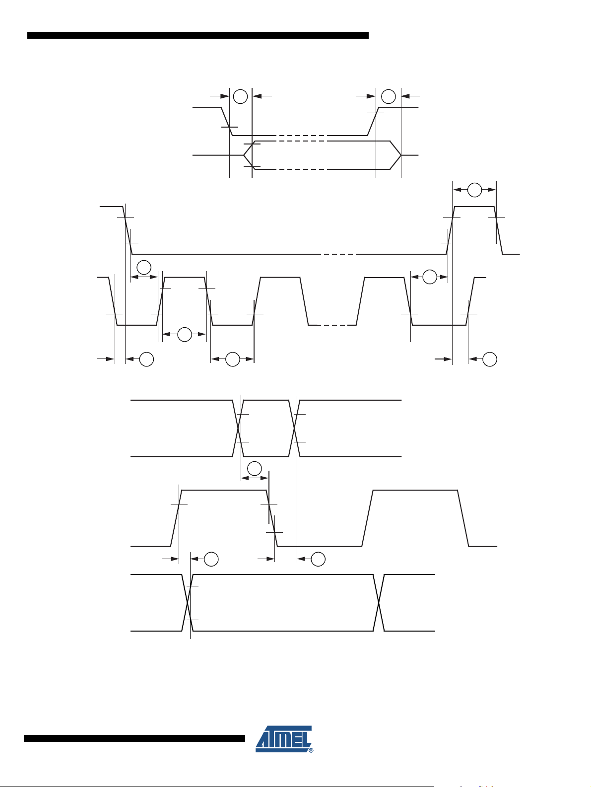
Figure 8-1. Serial Interface Timing Diagram with Chart Numbers
ATA6837 [Preliminary]
CS
CLK
1
CS
DO
4
5
3
6 8
2
9
7
DI
11
CLK
10 12
DO
Inputs DI, CLK, CS: High level = 0.7 × VCC, low level = 0.2 × V
Output DO: High level = 0.8 × V
, low level = 0.2 × V
CC
CC
CC
4953C–AUTO–09/07
13
Page 14

9. Noise and Surge Immunity
Parameters Test Conditions Value
Conducted interferences ISO 7637-1 Level 4
Interference suppression VDE 0879 Part 2 Level 5
ESD (Human Body Model) ESD S 5.1 4 kV
CDM (Charge Device Model) ESD STM5.3. 500V
Note: 1. Test pulse 5: V
vbmax
= 40V
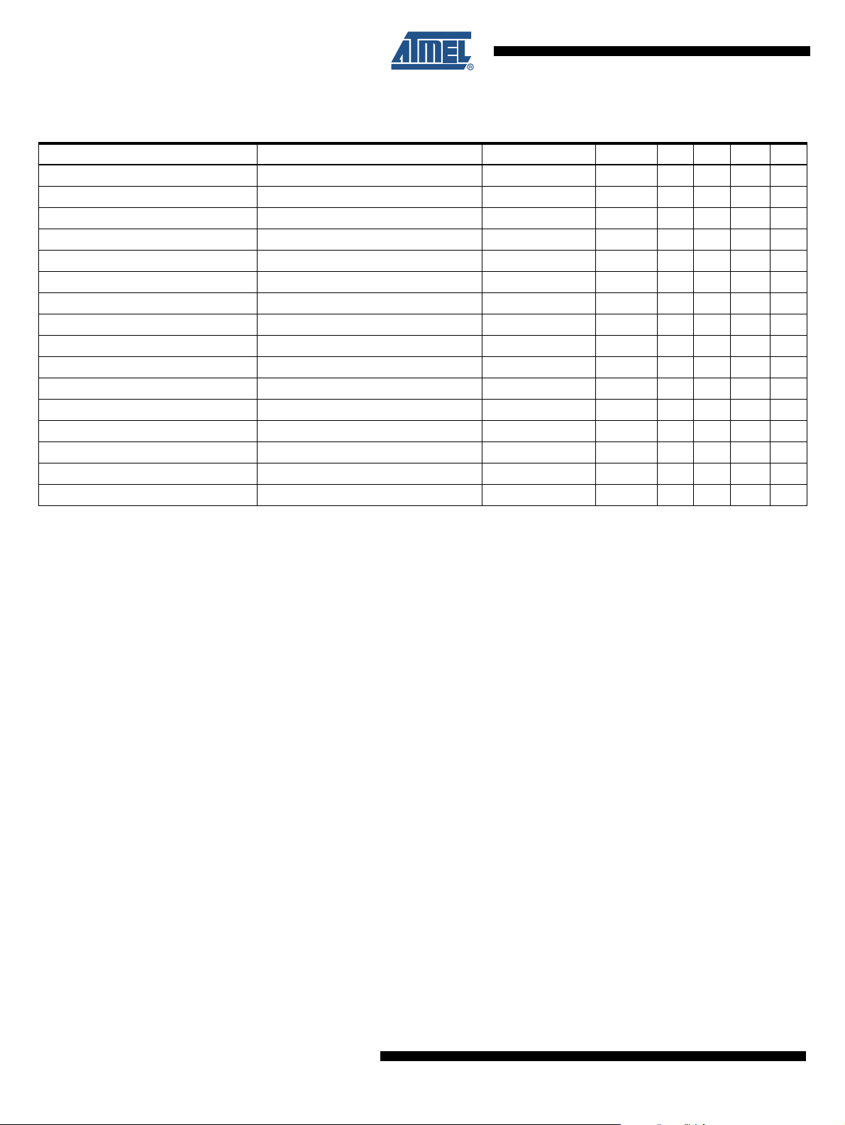
10. Application Circuit
Figure 10-1. Application Circuit
(1)
VCC
U5021M
Watchdog
Reset
Microcontroller
Trigger
Enable
VCC
CLK
CS
INH
DO
VS
GND
GND
VS
BYT41D
+
Vbatt
24V
S
O
C
L
S
T
D
I
Input register
Ouput register
P
I
S
S
N
DI
C
F
H
D
H
L
H
H
L
S
S
S
5
6
6
H
L
H
S
S
S
6
6
5
L
S
S
S
5
4
4
H
L
L
S
S
S
4
4
5
H
L
S
S
3
3
Serial interface
H
L
S
S
3
3
H
L
H
L
S
S
2
2
H
L
S
S
2
2
S
S
S
R
1
1
R
Charge
pump
H
L
T
S
S
P
1
1
GND
GND
VCC
VCC
VCC
5V
+
Fault
Detect
Fault
Detect
Fault
Detect
Fault
Detect
Fault
Detect
Fault
Detect
Control
logic
UV
protection
Power on
reset
GND
Fault
Detect
Fault
Detect
Fault
Detect
Fault
Detect
Fault
Detect
Fault
Detect
Thermal
protection
GND
GND
14
GND
OUT1 OUT3OUT2 OUT4 OUT5 OUT6
M M M M M
ATA6837 [Preliminary]
4953C–AUTO–09/07
Page 15

10.1 Application Notes
• Connect the blocking capacitors at VCC and VS as close as possible to the power supply and
• Recommended value for capacitors at V
• Recommended value for capacitors at VCC:
• To reduce thermal resistance, place cooling areas on the PCB as close as possible to GND
ATA6837 [Preliminary]
GND pins.
:
S
Electrolytic capacitor C > 22 µF in parallel with a ceramic capacitor C = 100 nF. Value for
electrolytic capacitor depends on external loads, conducted interferences and
reverse-conducting current I
Electrolytic capacitor C > 10 µF in parallel with a ceramic capacitor C = 100 nF.
pins and to the die paddle in QFN24.
(see Section 4. “Absolute Maximum Ratings” on page 8).
HSX
4953C–AUTO–09/07
15
Page 16

11. Ordering Information
Extended Type Number Package Remarks
ATA6837-PJQW QFN24 Taped and reeled, Pb-free
12. Package Information
Package: QFN 24 - 5 x 5
Exposed pad 3.6 x 3.6
(acc. JEDEC OUTLINE No. MO-220)
Dimensions in mm
Not indicated tolerances ±0.05
0.9±0.1
5
Drawing-No.: 6.543-5122.01-4
Issue: 1; 15.11.05
13. Revision History
Please note that the following page numbers referred to in this section refer to the specific revision
mentioned, not to this document.
Revision No. History
4953C-AUTO-09/07
4953B-AUTO-07/07
+0
0.05
-0.05
24
1
6
0.3
18
0.4
13
12 7
3.6
19 24
1
technical drawings
according to DIN
specifications
6
0.65 nom.
3.25
• Section 7 “Electrical Characteristics” numbers 5.15 and 5.16 on page 10
changed
• Section 9 “Noise and Surge Immunity” on page 14 changed
• Put datasheet in a new template
• Section 7 “Electrical Characteristics” numbers 1.5, 3.1, 5.15 and 8.2 on
pages 9 to 11 changed
16
ATA6837 [Preliminary]
4953C–AUTO–09/07
Page 17

Headquarters International
Atmel Corporation
2325 Orchard Parkway
San Jose, CA 95131
USA
Tel: 1(408) 441-0311
Fax: 1(408) 487-2600
Atmel Asia
Room 1219
Chinachem Golden Plaza
77 Mody Road Tsimshatsui
East Kowloon
Hong Kong
Tel: (852) 2721-9778
Fax: (852) 2722-1369
Product Contact
Web Site
www.atmel.com
Literature Requests
www.atmel.com/literature
Atmel Europe
Le Krebs
8, Rue Jean-Pierre Timbaud
BP 309
78054
Saint-Quentin-en-Yvelines Cedex
France
Tel: (33) 1-30-60-70-00
Fax: (33) 1-30-60-71-11
Technical Support
auto_control@atmel.com
Atmel Japan
9F, Tonetsu Shinkawa Bldg.
1-24-8 Shinkawa
Chuo-ku, Tokyo 104-0033
Japan
Tel: (81) 3-3523-3551
Fax: (81) 3-3523-7581
Sales Contact
www.atmel.com/contacts
Disclaimer: The information in this document is provided in connection with Atmel products. No license, express or implied, by estoppel or otherwise, to any
intellectual property right is granted by this document or in connection with the sale of Atmel products. EXCEPT AS SET FORTH IN ATMEL’S TERMS AND CONDI-
TIONS OF SALE LOCATED ON ATMEL’S WEB SITE, ATMEL ASSUMES NO LIABILITY WHATSOEVER AND DISCLAIMS ANY EXPRESS, IMPLIED OR STATUTORY
WARRANTY RELATING TO ITS PRODUCTS INCLUDING, BUT NOT LIMITED TO, THE IMPLIED WARRANTY OF MERCHANTABILITY, FITNESS FOR A PARTICULAR
PURPOSE, OR NON-INFRINGEMENT. IN NO EVENT SHALL ATMEL BE LIABLE FOR ANY DIRECT, INDIRECT, CONSEQUENTIAL, PUNITIVE, SPECIAL OR INCIDENTAL DAMAGES (INCLUDING, WITHOUT LIMITATION, DAMAGES FOR LOSS OF PROFITS, BUSINESS INTERRUPTION, OR LOSS OF INFORMATION) ARISING OUT OF
THE USE OR INABILITY TO USE THIS DOCUMENT, EVEN IF ATMEL HAS BEEN ADVISED OF THE POSSIBILITY OF SUCH DAMAGES. Atmel makes no
representations or warranties with respect to the accuracy or completeness of the contents of this document and reserves the right to make changes to specifications
and product descriptions at any time without notice. Atmel does not make any commitment to update the information contained herein. Unless specifically provided
otherwise, Atmel products are not suitable for, and shall not be used in, automotive applications. Atmel’s products are not intended, authorized, or warranted for use
as components in applications intended to support or sustain life.
© 2007 Atmel Corporation. All rights reserved. Atmel®, logo and combinations thereof, and others are registered trademarks or trademarks of
Atmel Corporation or its subsidiaries. Other terms and product names may be trademarks of others.
4953C–AUTO–09/07
 Loading...