

Page 1
Features
• ATA6833 Temperature Range T
• ATA6834 Extended Temperature Range T
• Direct Driving of 6 External NMOS Transistors with a Maximum Switching Frequency of
50 kHz
• Integrated Charge Pump to Provide Gate Voltages for High-side Drivers and to Supply
the Gate of the External Battery Reverse Protection NMOS
• Built-in 5V/3.3V Voltage Regulator with Current Limitation
• Reset Signal for the Microcontroller
• Sleep Mode with Supply Current of typically < 45 µA
• Wake-up via LIN Bus or High Voltage Input
• Programmable Window Watchdog
• Battery Overvoltage Protection and Battery Undervoltage Management
• Overtemperature Warning and Protection (Shutdown)
• 200 mA Peak Current for Each Output Driver
• LIN Transceiver Conformal to LIN 2.1 and SAEJ2602-2 with Outstanding EMC and ESD
Performance
• QFN48 Package 7 mm × 7 mm
= 125°C, TJ = 150°C
A
= 150°C, TJ = 200°C
A
BLDC Motor
Driver and LIN
System Basis
Chip
ATA6833
1. Description
The ATA6833 and ATA6834 are system basis chips for three-phase brushless DC
motor controllers designed in Atmel
SMART-I.S.
FETs, the system basis chip forms a BLDC motor control unit for automotive
applications. In addition, the circuits provide a 3.3V/5V linear regulator and a window
watchdog.
The circuit includes various control and protection functions like overvoltage and overtemperature protection, short circuit detection, and undervoltage management.
Thanks to these function blocks, the driver fulfils a maximum of safety requirements
and offers a high integration level to save cost and space in various applications. The
target applications are most suitable for the automotive market due to the robust technology and the high qualification level. ATA6834, in particular, is designed for
applications in a high-temperature environment.
™
1. In combination with a microcontroller and six discrete power MOS-
®
’s state-of-the-art 0.8 µm SOI technology
ATA6834
Preliminary
9122B–AUTO–10/08
Page 2
Figure 1-1. Block Diagram
Supervisor:
Short Circuit
Overtemperature
Undervoltage
CP
VBATSW VINTVBAT
VBAT
PBAT
VG
LIN EN1
CPLO2CPLO1
CPOUTCPHI2CPHI1
CC
Timer
WD
Timer
VBG
LIN
Hall A
Hall B
Hall C
ATA6833/34
Logic Control
Oscillator
VINT 5V
Regulator
13V
Regulator
Microcontroller
High-side
Driver 1
High-side
Driver 2
High-side
Driver 3
3.3/5V VCC
Regulator
Low-side
Driver 3
Low-side
Driver 2
Low-side
Driver 1
L2
L1
L3
VMODE
H2
H3
DG3
/RESET
DG2
DG1
WD
IH1-3
IL1-3
TX
RX
VCC
H1
S2
S3
S1
RWD WDDGNDEN2 PGND
M
Hall A
Hall C
Hall B
CC
2
ATA6833/ATA6834 [Preliminary]
9122B–AUTO–10/08
Page 3
2. Pin Configuration
Figure 2-1. Pinning QFN48
VMODE
VINT
RWD
CC
/RESET
WD
WDD
EN1
NC
NC
GND
NC
ATA6833/ATA6834 [Preliminary]
VG
L1
L2
L3
VBAT
EN2
VBATSW
48 47 46 45 44 43 42 41 40 39 38 37
1
2
3
4
5
6
ATA6833/ATA6834
7
8
9
10
11
12
13 14 15 16 17 18 19 20 21 22 23 24
NC
LIN
TXD
PGND
NC
VCC
Atmel YWW
ZZZZZ-AL
IL2
IL3
IH3
IH2
IL1
IH1
RXD
NC
PBAT
36
35
34
33
32
31
30
29
28
27
26
25
DG1
CPLO1
CPHI1
CPLO2
CPHI2
CPOUT
S1
H1
S2
H2
S3
H3
DG3
DG2
Note: YWW Date code (Y = Year - above 2000, WW = week number)
ATA683x Product name
ZZZZZ Wafer lot number
AL Assembly sub-lot number
Table 2-1. Pin Description
Pin Symbol I/O Function
1 VMODE I Selector for V
2 VINT I/O Blocking capacitor
3 RWD I Resistor defining the watchdog interval
4 CC I/O RC combination to adjust cross conduction time
5 /RESET O Reset signal for microcontroller
6 WD I Watchdog trigger signal
7 WDD I Enable and disable the watchdog
8 EN1 I Microcontroller output to switch system in Sleep Mode
9 N.C. Connect to GND
10 N.C. Connect to GND
11 GND I Ground
12 NC Connect to GND
13 LIN I/O LIN-bus terminal
14 NC Connect to GND
15 TXD I Transmit signal to LIN bus from microcontroller
16 IL3 I Control Input for output L3
17 IH3 I Control Input for output H3
and interface logic voltage level
CC
9122B–AUTO–10/08
3
Page 4
Table 2-1. Pin Description
Pin Symbol I/O Function
18 IL2 I Control Input for output L2
19 IH2 I Control Input for output H2
20 IL1 I Control Input for output L1
21 IH1 I Control Input for output H1
22 RXD O Receive signal from LIN bus for microcontroller
23 DG1 O Diagnostic output 1
24 DG2 O Diagnostic output 2
25 DG3 O Diagnostic output 3
26 H3 O Gate voltage high-side 3
27 S3 I/O Voltage at half bridge 3
28 H2 O Gate voltage high-side 2
29 S2 I/O Voltage at half bridge 2
30 H1 O Gate voltage high-side 1
31 S1 I/O Voltage at half bridge 1
32 CPOUT I/O Charge pump output capacitor
33 CPHI2 I Charge pump capacitor 2
34 CPLO2 O Charge pump capacitor 2
35 CPHI1 I Charge pump capacitor 1
36 CPLO1 O Charge pump capacitor 1
37 NC Connect to GND
38 PBAT I Power supply (after reverse protection) for charge pump and gate drivers
39 VG I/O Blocking capacitor
40 L1 O Gate voltage H-bridge, low-side 1
41 L2 O Gate voltage H-bridge, low-side 2
42 L3 O Gate voltage H-bridge, low-side 3
43 PGND I Power ground for H-bridge and charge pump
44 VCC O 5V/100 mA supply for microcontroller
45 NC Connect to GND
46 VBAT I Supply voltage for IC core (after reverse protection)
47 EN2 I High voltage enable input
48 VBATSW O 100Ω PMOS switch from V
BAT
4
ATA6833/ATA6834 [Preliminary]
9122B–AUTO–10/08
Page 5

ATA6833/ATA6834 [Preliminary]
3. Functional Description
3.1 Power Supply Unit with Supervisor Functions
3.1.1 Power Supply
The IC has to be supplied by a reverse-protected battery voltage. To prevent damage to the IC,
proper external protection circuitry has to be added. It is recommended to use at least one
capacitor combination of storage and RF capacitors behind the reverse protection circuitry,
which is connected close to the VBAT and GND pins of the IC.
A fully integrated low-power and low-drop regulator (VINT regulator), stabilized by an external
blocking capacitor, provides the necessary low-voltage supply needed for the wake-up process.
A trimmed low-power band gap is used as reference for the VINT regulator as well as for the
VCC regulator. All internal blocks are supplied by VINT regulator. VINT regulator must not be
used for any external supply purposes.
Nothing inside the IC except the logic interface to the external microcontroller is supplied by the
5V/3.3V VCC regulator.
Both voltage regulators are checked by a “power-good comparator”, which keeps the whole chip
in reset as long as the internal supply voltage (VINT regulator output) is too low and generates a
reset for the external microcontroller if the output voltage of the VCC regulator is not sufficient.
3.1.2 VBatt Switch
This high-voltage switch provides the battery voltage at pin VBATSW for various purposes. It is
switched ON after power on reset when the IC transits to Active Mode and it will only turn OFF
when the IC changes to Sleep Mode. Watchdog resets do not have an effect on the switch. The
switch can be used for measuring purposes as well as to switch on external voltage regulators.
3.1.3 Voltage Supervisor
This function is implemented to protect the IC and the external power MOS transistors from
damage due to overvoltage on PBAT input. In the event of overvoltage (V
(V
), the external NMOS motor driver transistors will be switched off. The failure state will be
THUV
flagged on DG2 pin. It is recommended to block PBAT with an external RF capacitor to suppress
high frequency disturbances.
3.1.4 Temperature Supervisor
An integrated temperature sensor prevents the IC from overheating. If the temperature is above
the overtemperature pre-warning threshold T
HIGH to signal this event to the external microcontroller. The microcontroller should take actions
to reduce the power dissipation in the IC. If the temperature rises above the overtemperature
shutdown threshold T
transceiver will be switched OFF immediately and the /RESET signal will go LOW. Both thresholds have a built-in hysteresis to avoid oscillations. The IC will return to normal operation (Active
Mode) when it has cooled down below the shutdown threshold. When the junction temperature
drops below the pre-warning threshold, bit DG3 will be switched LOW.
J switch off
) or undervoltage
THOV
, the diagnostic pin DG3 will be switched to
JPW set
, the VCC regulator and all output drivers together with the LIN
9122B–AUTO–10/08
5
Page 6
3.2 Active Mode and Sleep Mode
Sleep Mode
LIN
VCC
EN1
Active ModeActive Mode
T
bus
= 90 µs Regulator Wake-up Time = 4 × T
OSC
T
gotosleep
= 10 µs
T
debounce
The IC has two modes: Sleep Mode and Active Mode. Switching between the modes is
described below. By default the IC starts in Active Mode (which means normal operation) after
power-on. A Go to Sleep procedure switches the IC from Active Mode to Sleep Mode (standby).
A Go to Active procedure brings the IC back from Sleep Mode to Active Mode. When in Sleep
Mode the internal 5V supply (VINT regulator), the EN2 pin input structure, and a certain part of
the LIN receiver remain active to ensure a proper startup of the system. The VCC regulator is
turned off.
The Go to Sleep and Go to Active procedures are implemented as follows:
Go to Sleep:
Pin EN1 is a low-voltage input supplied by the VCC regulator. It is ESD protected by diodes
against VCC and GND. Thus the input voltage at pin EN1 must not go below GND or exceed the
output voltage of the VCC regulator. A transition from HIGH to LOW followed by a permanent
LOW signal for a minimum time period t
Sleep Mode as the EN1 is edge triggered. V
to keep EN1 LOW during normal operation.
Go to Active Using Pin EN2:
Pin EN2 is a high-voltage input for external wake-up signals. Its input structure consists of a
comparator with a built-in hysteresis. It is ESD-protected by diodes against GND and V
and for this reason the applied input voltage must not go below GND or exceed V
EN2 up to V
Go to Active Using the LIN Interface:
switches the IC to Active Mode. EN2 is debounced and edge triggered.
BAT
gotosleep
(typical 10 µs) at pin EN1 switches the IC to
is switched off in Sleep Mode. It is recommended
CC
BAT
, B,
BAT
. Pulling
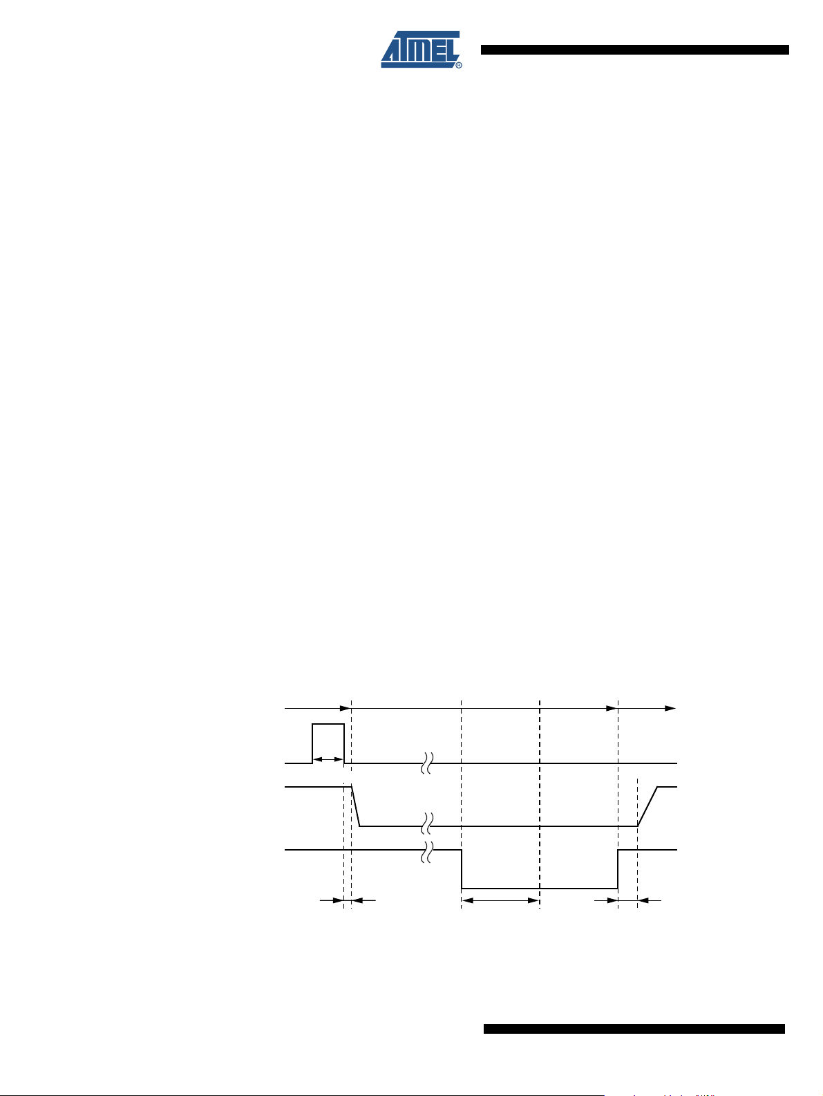
Using the LIN interface provides a second possibility to wake-up the IC (see Figure 3-1). A falling edge at pin LIN followed by a dominant bus level maintained for a minimum time period
(T
) and ending with a rising edge leads to a remote wake-up request. The device switches
bus
from Sleep Mode to Active Mode. The VCC regulator is activated and the internal LIN slave termination resistor is switched on.
Figure 3-1. Wake-up Using the LIN Interface
6
ATA6833/ATA6834 [Preliminary]
9122B–AUTO–10/08
Page 7
ATA6833/ATA6834 [Preliminary]
0
5
10
15
20
25
30
35
40
0255075100125150
Load Current (mA)
ESR (Ω)
ESR versus Load Current at Pin VCC
ESR
min
(C
VCC
= 2.2 µF)
ESR
max
(C
VCC
= 2.2 µF)
0
5
10
15
20
25
0255075100125150
ESR (Ω)
Load Current (mA)
ESR versus Load Current at Pin VCC
ESR
max
(C
VCC
= 10 µF)
ESR
min
(C
VCC
= 10 µF)
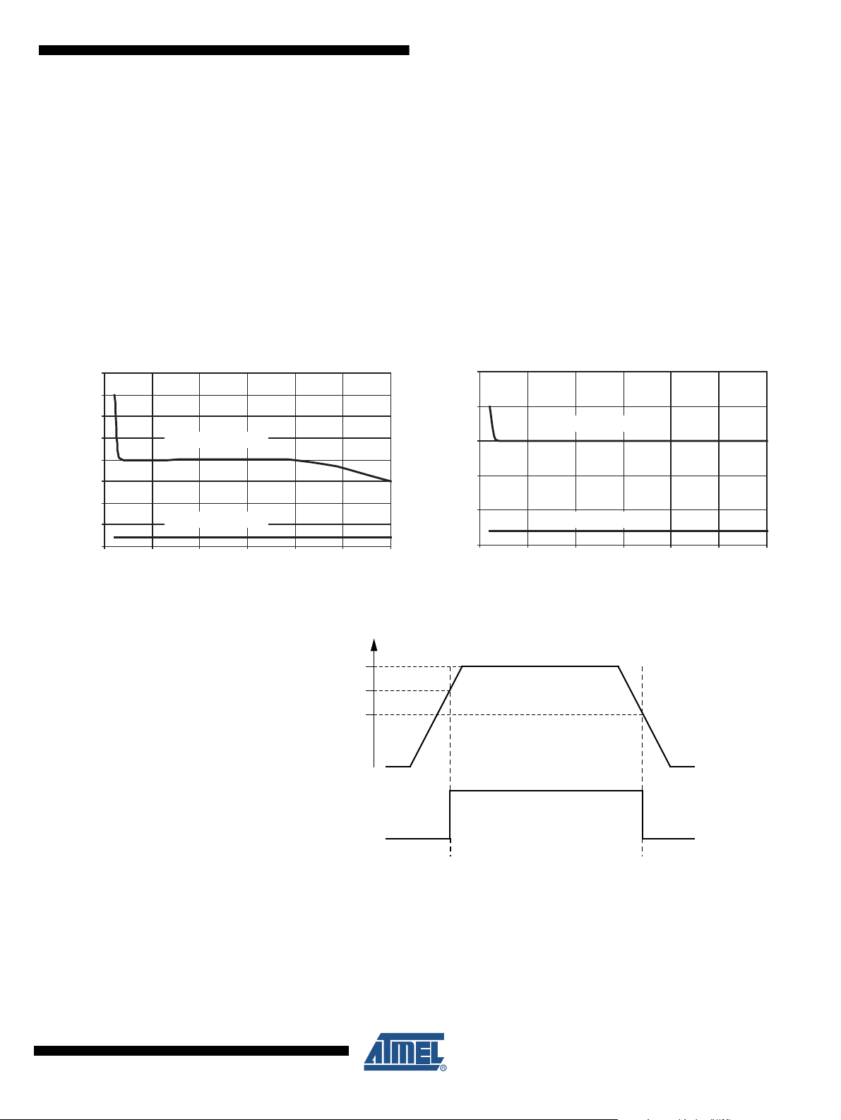
3.3 5V/3.3V VCC Regulator
The 5V/3.3V regulator is fully integrated. It requires an external electrolytic capacitor in the range
of 2.2 µF up to 10 µF and with an ESR in the range from 2Ω to 15Ω for stability (see Figure 3-2).
The output voltage can be configured as either 5V or 3.3V by connecting pin VMODE to either
pin VINT or GND. Since the regulator is not designed to be switched between both output voltages during operation, it is advisable to hard-wire VMODE pin. The logic levels of the
microcontroller interface are adapted to the VCC regulator output voltage. The maximum output
current (I
80 mA. The VCC regulator has a built-in short circuit protection. A comparator checks the output
voltage of the VCC regulator and keeps the external microcontroller in reset as long as the voltage is below the lower operation minimum (shown in Figure 3-33).
Figure 3-2. ESR versus Load Current for External Capacitors with Different Values
) of the regulator is 100 mA. For TJ> 150°C the I
OS1
of ATA6834 is reduced to
OS1
Figure 3-3. /RESET as Function of the VCC Output Voltage
100% VCC
9122B–AUTO–10/08
VCC
88% VCC
80% VCC
/RESET
0V
7
Page 8
3.4 Reset and Watchdog Management
Watchdog
trigger edge
Reset and lead
time, no trigger
Watchdog cycle,
no trigger
Watchdog cycle, trigger
during t
2
window
Reset and lead time,
trigger during lead time
t
resshort
t
1
t
2
t
1
t
d
t
res
t
d
t
1
t
res
t
2
Watchdog trigger
in t
2
window
88% VCC
VCC
WD
/RESET
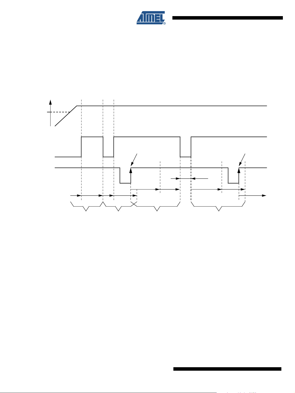
The watchdog timing is based on the trimmed internal watchdog oscillator. Its period time T
is determined by the external resistor RWD. A HIGH signal on WDD pin enables the watchdog
function; a LOW signal disables it. Since WDD pin is equipped with an internal pull-up resistor
the watchdog is enabled by default. In order to keep the current consumption as low as possible
the watchdog is switched off during Sleep Mode.
The timing diagram in Figure 3-4 shows the watchdog and external reset timing.
Figure 3-4. Timing Diagram of the Watchdog in Conjunction with the /RESET Signal
OSC
8
After power-up of the VCC regulator (VCC output exceeds 88% of its nominal value) /RESET
output stays LOW for the timeout period t
res
switches to HIGH. During the following time t
expected otherwise another external reset will be triggered.
When the watchdog has been correctly triggered for the first time, normal watch-dog operation
begins. A normal watchdog cycle consists of two time sections t
for the time t
edges on WD pin during t
at /RESET if no valid trigger has been applied at pin WD during t2. Rising
resshort
also cause a short pulse on /RESET. Start for such a cycle is always
1
the time of the last rising edge either on WD pin or on /RESET pin.
If the watchdog is disabled (WDD = LOW), only the initial reset for the time t
will be generated.
Additional resets will be generated if the VCC output voltage drops below 80% of its nominal
value.
The following example demonstrates how to calculate the timing scheme for valid watchdog trigger pulses, which the external microcontroller has to provide in order to prevent undesired
resets.
ATA6833/ATA6834 [Preliminary]
(typical 10 ms). Subsequently /RESET output
(typical 500 ms) a rising edge at the input WD is
d
and t2 followed by a short pulse
1
after power-up
res
9122B–AUTO–10/08
Page 9

Example:
)
ATA6833/ATA6834 [Preliminary]
Using an external resistor R
T
= 12.32 µs
OSC
t
=980 × T
1
t
=780 × T
2
t
+ t2 = 21.68 ms ±10%
1
= 12.07 ms ±10%
OSC
= 9.609 ms ±10%
OSC
=33kΩ ±1% results in typical parameters as follows:
WD
Hence, the minimum time the external microcontroller has to wait before pin WD can be triggered is in worst case t
WD pin is t
t
max–tmin
=0.9× (t1+t2) = 19.51 ms. Thus watchdog trigger input must remain within
max
= 6.23 ms.
Other values can be set up by picking a different resistor value for R
=1.1× t1= 13.28 ms. The maximum time for the watchdog trigger on
min
. The dependency of T
WD
OSC
on the value of RWD is shown in Figure 3-5.
Figure 3-5. T
versus R
OSC
(µs)
OSC
T
WD
45
40
35
30
25
20
15
10
5
0
10 20 30 40 50 60 70 80 90 100
T
(µs)
OSCmax
RWD (kΩ)
T
OSCmin
(µs)
T
(µs
OSC
3.5 Charge Pump
9122B–AUTO–10/08
A charge pump has been implemented in order to provide sufficient voltage to operate the external high-side power-NMOS transistors and the VG regulator, which drives the low-side
Power-NMOS transistors. The charge pump output voltage at CPOUT pin is controlled to settle
typically about 15V above the voltage at pin PBAT. A built-in supervisor circuit checks if the output voltage is sufficient to operate the VG regulator and external Power-NMOS transistors. The
output voltage is accepted as good when it rises above VCP
CPGOOD
. A charge pump failure is
flagged at DG2 if this minimum can not be reached or if the output voltage drops below the lower
threshold of VCP
CPGOOD
due to overloading.
The two shuffle capacitors should have the same value. The value of the reservoir capacitor
should be at least twice the value of one shuffle capacitor. Two external shuffle capacitors and
an external reservoir capacitor have to be provided. The typical values for the two shuffle capacitor is 100F, and for the reservoir capacitor is 470 nF. All capacitors should be ceramic. It is
advisable to pick a reservoir capacitor with twice or three-times the size of the two equally-sized
shuffle capacitors. The greater the capacitors, the greater the output current capability.
9
Page 10

3.6 VG Regulator
The VG regulator provides a stable voltage to supply the low-side gate drivers and to deliver sufficient voltage for the external low-side Power-NMOS transistors. Typically the output voltage is
12V. In order to guarantee reliable operation even with a low battery voltage, the VG regulator is
supplied by the charge pump output. For stability, an external ceramic capacitor of typically
470 nF has to be provided. There is no internal supervision of the VG output voltage.
3.7 Output Drivers and Control Inputs IL1-IL3, IH1-IH3
This IC offers six push-pull output drivers for the external low-side and high-side power-NMOS
transistors. To guarantee reliable operation, the low-side drivers are supplied by the VG regulator while the high-side drivers are supplied directly by the charge pump. All drivers are designed
to operate at switching frequencies in the range of DC up to 50 kHz. The maximum gate charge
that can be delivered to each external Power-NMOS transistor at 50 kHz is 100 nC.
The output drivers are directly controlled by the digital input pins IL1 to IL3 and IH1 to IH3 (see
Table 3-1). All pins are equipped with an internal pull-down resistor. To operate the output driv-
ers properly the following requirements have to be fulfilled:
1. Device is in Active Mode.
2. In case of watchdog is enabled, at least one valid watchdog trigger has been accepted.
3. The voltage at pin PBAT lies within its operation range. Neither undervoltage nor overvoltage is present.
4. The charge pump output voltage has been accepted as good, thus it exceeded
VCP
CPGOOD
5. No overtemperature shutdown has occurred.
If a short circuit is detected by one of the sense inputs S1 to S3, the output drivers will be
switched off after a debounce time of 6 µs and the output DG1 will be flagged (see also Section
3.8 “Short Circuit Detection” on page 11). The output drivers will be enabled again and DG1 will
be cleared with a rising edge at one of the control inputs (IL1 to IL3, IH1 to IH3).
.
10
Additional logic prevents short circuits due to switching on one power-NMOS transistor while the
opposite one in the same branch is switched on already.
Table 3-1. Status of the Output Drivers Depending on the Control Inputs
Control
Inputs
Mode
Sleep X X OFF Sleep Mode
Active 0 0 OFF
Active 1 0 L[1..3] ON, H[1..3] OFF
Active 0 1 H[1..3] ON, L[1..3] OFF
Active 1 1 OFF Shoot-through protection
IL[1..3]
Control
Inputs
IH[1..3]
Driver Stage for External
ATA6833/ATA6834 [Preliminary]
Power MOS
L[1..3], H[1..3] Comments
9122B–AUTO–10/08
Page 11

3.8 Short Circuit Detection
Short circuits in the motor bridge circuitry are sensed by S1 to S3 inputs. Internal comparators
monitor the voltage differences between the drain and the source terminals of the external
power-NMOS transistors. If one transistor switches on and the voltage drop from its drain to
source stays higher than the threshold V
a short circuit in this branch is detected. In this case, all output drivers are switched off immediately and DG1 pin will be set to HIGH. With a rising edge at any of the pins IL1 to IL3 or IH1 to
IH3, the diagnostic output DG1will be reset and the drivers can be switched on again.
3.9 Cross Conduction Timer
In order to prevent damage of the motor bridge due to peak currents a non-overlapping phase
for switching the power-NMOS transistors is mandatory. Therefore, a cross conduction timer has
been implemented to prevent switching on any output driver for a time t
has been switched off. This also accounts for toggling any other driver after a short circuit was
detected. An external RC parallel combination defines the value for t
follows:
t
= KCC × RCC [kΩ] × CCC [nF], KCC is specified in Section 8. “Electrical Characteristics” on
CC
page 15.
ATA6833/ATA6834 [Preliminary]
(typical 4V) for a longer time than tSC (typically 6 µs),
SC
after any other driver
CC
and can be estimated as
CC
The RC combination is connected between CC and GND pins. When one of the drivers has
been switched off the RC combination is charged to 5V (VINT) and discharged with its time constant. Any low to high transition at the control inputs will be masked out at the driver outputs until
the voltage at CC pin drops below 67% of its initial value (VINT). The timer will be re-triggered at
any time by any falling edge at the control inputs. This is shown in the following figure.
Figure 3-6. Timing Scheme of the Cross Conduction Timer
IL1
L1
IH1
H1
IL3
L3
V
= V
CC
VINT
CC
V
= 67% V
CC
VINT
t
cc
t
cc
t
cc
9122B–AUTO–10/08
At least 5 kΩ minimum and 5 nF at maximum should be used as values for the RC combination.
10 kΩ is recommended. If the non-overlapping phase is controlled by the external microcon-
troller, it is possible to do without the external capacitor. The minimum time t
is defined by the
CC
parasitic capacitance at CC pin.
11
Page 12

3.10 Diagnostic Outputs D1 - D3
As mentioned in the sections above, the diagnostic outputs DG1 to DG3 are used to signal failures. This is summarized in the following table.
Table 3-2. Status of the Diagnostic Outputs (Normal Operation)
Device Status Diagnostic Outputs Comments
CPOK OT1 OV UV SC DG1 DG2 DG3
0 X X X X – 1 – Charge pump failure
X 1 X X X – – 1 Overtemperature prewarning
X X 1 X X – 1 – Overvoltage
X X X 1 X – 1 – Undervoltage
X X X X 1 1 – – Short circuit
Note: X represents: no effect)
OT1: overtemperature warning
OV: overvoltage of PBAT
UV: undervoltage of PBAT
SC: short circuit
CPOK: charge pump OK
In order to differentiate between LIN and EN2 wake-up, DG1 output will be set to LOW or HIGH
respectively. LOW indicates wake-up by LIN, HIGH indicates wake-up by EN2. DG1 output will
be cleared by the first valid watchdog trigger after wake-up or by the first rising edge at one of
the control inputs (IL1 to IL3 and IH1 toIH3) if the watchdog is disabled.
3.11 LIN Transceiver
Table 3-3. Indicating Wake-up Source
Diagnostic Outputs
Wake-up SourceDG1 DG2 DG3
1–– EN2
0–– LIN
ATA6833 and ATA6834 include a fully integrated LIN transceiver complying with LIN specification 2.1 and SAEJ2602 2. The transceiver consists of a low-side driver with slew rate control,
wave shaping, current limiting, and a high voltage comparator followed by a debouncing unit in
the receiver.
During transmission, the data applied at pin TXD will be transferred to the bus driver to generate
a bus signal on LIN pin. TXD input has an internal pull-up resistor.
To minimize the electromagnetic emission of the bus line, the bus driver has a built-in slew rate
control and wave-shaping unit. The transmission will be aborted by a thermal shutdown or by a
transition to Sleep Mode.
12
ATA6833/ATA6834 [Preliminary]
9122B–AUTO–10/08
Page 13

Figure 3-7. Definition of Bus Timing Parameters
ATA6833/ATA6834 [Preliminary]
(Input to transmitting node)
TXD
VS
(Transceiver supply
of transmitting node)
RXD
(Output of receiving node1)
TH
TH
TH
TH
Rec(max)
Dom(max)
Rec(min)
Dom(min)
t
rx_pdf(1)
t
Bit
t
Bus_dom(max)
LIN Bus Signal
t
Bus_dom(min)
t
Bit
t
Bus_rec(min)
t
Bit
Thresholds of
receiving node1
Thresholds of
receiving node2
t
Bus_rec(max)
t
rx_pdr(1)
(Output of receiving node2)
RXD
The recessive BUS level is generated from the integrated 30 kΩ pull-up resistor in series with an
active diode. This diode protects against reverse currents on the bus line in case of a voltage difference between the bus line and VSUP (V
necessary to use the IC as a LIN slave. If this IC is used as a LIN master, the LIN pin is terminated by an external 1 kΩ resistor in series with a diode to VBAT.
As PWM communication directly over the LIN transceiver in both directions is possible, there is
no TXD timeout feature implemented in the LIN transceiver.
t
rx_pdr(2)
BUS
> V
t
rx_pdf(2)
). No additional termination resistor is
SUP
9122B–AUTO–10/08
13
Page 14

4. Absolute Maximum Ratings
Stresses beyond those listed under “Absolute Maximum Ratings” may cause permanent damage to the device. This is a stress rating
only and functional operation of the device at these or any other conditions beyond those indicated in the operational sections of this
specification is not implied. Exposure to absolute maximum rating conditions for extended periods may affect device reliability.
All voltages are referenced to pin GND. [xxx] Values for the ATA6834.
Parameters Pin Symbol Min. Max. Unit
Input voltage PGND V
PGND
Negative input current VBAT IVBAT TBD TBD mA
Negative input current PBAT IPBAT TBD TBD mA
Supply voltage VBAT V
Supply voltage PBAT V
Logic output voltage
Logic input voltage
/RESET, DG1,
DG2, DG3, RXD
IL1-3, IH1-3, WD,
WDD, EN1, TXD
V
V
Output voltage VINT, VCC V
Analog input voltage RWD, CC V
Digital input voltage EN2 V
Digital input voltage VMODE V
Output voltage VG V
Input voltage LIN V
Output voltage S1, S2, S3 V
Output voltage L1, L2, L3 V
Output voltage H1, H2, L3 V
Charge pump CPLO1, 2 V
Charge pump CPHI1, 2 V
Output voltage CPOUT V
Output voltage VBATSW V
Storage temperature T
/RESET
V
IL1-3
V
S1
L1
H1
CPLO1
CPHO1
VBAT
PBAT
, V
DG1
, V
DG3
, V
IH1-3
, V
EN1
, V
INT
RWD
EN2
VMODE
VG
VLIN
, VS2, V
, VL2, V
, VH2, V
, V
, V
CPOUT
VBATSW
Storage
, V
RXD
, VWD,
TXD
VVCC
CPLO2
CPHO2
S3
L3
H3
DG2
,
–0.3 +0.3 V
–0.3 +40 (500 ms) V
–0.3 +40 (500 ms) V
–0.3 V
–0.3 V
+ 0.3 V
VCC
+ 0.3 V
VCC
–0.3 +5.5 V
–0.3 V
–0.3 V
–0.3 V
+ 0.3 V
VCC
+ 0.3 V
VBAT
+ 0.3 V
VINT
–0.3 +16 V
–27 V
+ 2 V
VBAT
–6 +30 V
V
– 0.3 V
PGND
V
– 1 V
S1, 2, 3
–0.3 V
–0.3 V
+ 0.3 V
VG
+ 16 V
S1, 2, 3
+ 0.3 V
PBAT
+ 0.3 V
CPOUT
–0.3 +40 V
–0.3 V
+ 0.3 V
VBAT
–55 +150 °C
5. Thermal Resistance
Parameters Symbol Value Unit
Thermal resistance junction to heat slug R
Thermal resistance junction to ambient when heat slug
is soldered to PCB
14
ATA6833/ATA6834 [Preliminary]
thjc
R
thja
<5 K/W
25 K/W
9122B–AUTO–10/08
Page 15

ATA6833/ATA6834 [Preliminary]
6. Operating Range
The operating conditions define the limits for functional operation and parametric characteristics of the device. Functionality outside these
limits is not implied unless otherwise stated explicitly. [xxx] Values for the ATA6834
Parameters Symbol Min Max Unit
Operating supply voltage
Operating supply voltage
Operating supply voltage
(1)
(2)
(3)
(t = 500 ms) V
Ambient temperature range T
Junction temperature range T
V
V
VBAT
VBAT
VBAT
A
J
5.5 V
4.3 5.5 V
(4)
V
THOV
–40 +150 °C
–40 +150 (200) °C
Notes: 1. Full functionality
2. Output drivers are switched off, extended range for parameters for voltage regulators
3. Output drivers and charge pump are switched off
4. Voltages higher V
for maximum 500 ms
THOV
7. Noise and Surge Immunity
Parameters Standard and Test Conditions Value
Conducted interferences ISO 7637-1 Level 4
Conducted disturbances CISP25 Level 5
ESD (Human Body Model) ESD S 5.1 ±2 kV
ESD (Human Body Model) DIN EN61000-4-2, Pin LIN, VBAT, PBAT to GND ±6 kV
Latch-up immunity JESD78, AEL-Q100 (004) Class II, level A
Note: 1. Test pulse 5: V
bat max
= 40V
(4)
THOV
40 V
(1)
V
8. Electrical Characteristics
All parameters given are valid for 5.5V ≤V
GND. [xxx] Values for the ATA6834.
No. Parameters Test Conditions Pin Symbol Min. Typ. Max. Unit Type*
1 Power Supply and Supervisor Functions
1.1 Current consumption V
Current consumption V
1.3
in Standby Mode
Current consumption V
1.4
in Standby Mode
1.5 Internal power supply V
VBATVVBAT
VBAT
V
VBAT
VBAT
V
PBAT
VBAT
1.6 Overvoltage threshold PBAT V
Overvoltage threshold
1.7
hysteresis
1.8 Undervoltage threshold PBAT V
Undervoltage threshold
1.9
hysteresis
V
1.10 R
VBAT-Switch switch
DSON
VBAT
I
VBATSW
*) Type means: A = 100% tested, B = 100% correlation tested, C = Characterized on samples, D = Design parameter
≤ 18V and for –40°C ≤ TJ ≤ 150°C (200°C) unless stated otherwise. All values refer to PIN
VBAT
= 13.5V
= 13.5V VBAT I
= 13.5V PBAT I
> 7V VINT V
= 13.5V,
(1)
= –15 mA
VBAT I
PBAT V
PBAT V
VBATSW R
VBAT
VBAT
VPBAT
VINT
THOV
TOVhys
THUV
TUVhys
ON_VBATSW
7mAA
65 µA A
TBD µA A
4.7 5.0 5.3 V A
19.8 22.3 V A
11.5VA
5.0 5.5 V A
0.2 0.4 V A
100 Ω A
9122B–AUTO–10/08
15
Page 16

8. Electrical Characteristics (Continued)
All parameters given are valid for 5.5V ≤V
GND. [xxx] Values for the ATA6834.
No. Parameters Test Conditions Pin Symbol Min. Typ. Max. Unit Type*
1.11 Thermal prewarning set T
1.12 Thermal prewarning reset T
Thermal prewarning
1.13
hysteresis
1.14 Thermal shutdown off T
1.15 Thermal shutdown on T
Thermal shutdown
1.16
hysteresis
Ratio thermal shutdown
1.17
off/thermal prewarning set
Ratio thermal shutdown
1.18
on/thermal prewarning
reset
2 5V/3.3V Regulator
V
MODE=VINT
2.1 Regulated output voltage
2.2 Regulated output voltage
V
MODE
I
Load
V
MODE=VINT
V
MODE
I
Load
150°C < TJ<200°C
V
2.3 Regulated output voltage
2.4 Regulated output voltage
MODE=VINT
V
MODE
I
Load
V
MODE=VINT
V
MODE
I
Load
150°C < T
V
2.5 Line regulation
2.6 Load regulation
MODE=VINT
V
MODE
I
Load
V
MODE=VINT
V
MODE
I
Load
I
Load
150°C < T
V
2.7 Output current limit
MODE=VINT
V
MODE
I
Load
*) Type means: A = 100% tested, B = 100% correlation tested, C = Characterized on samples, D = Design parameter
≤ 18V and for –40°C ≤ TJ ≤ 150°C (200°C) unless stated otherwise. All values refer to PIN
VBAT
, 7V < V
BAT
= GND, 5.5V < V
< 40V
<40V
BAT
JPW set
JPW reset
ΔT
J switch off
J switch on
ΔT
J switch off
T
J switch off
T
JPW set
T
J switch on
T
JPW reset
JPW
120
(170)
105
(155)
150
(200)
135
(185)
/
1.05 1.15 B
/
1.05 1.15 B
4.85
V
CC
V
VCC
3.20
145
(195)
130
(180)
170
(220)
155
(205)
15 °C B
175
(225)
160
(210)
200
(250)
185
(235)
15 °C B
5.15
3.40 V A
= 0 to 100 mA
, 7V < V
= GND, 5.5V < V
=0to80mA
, 5.5V < V
=GND, 5V<V
BAT
BAT
BAT
< 40V
<40V
BAT
<7V
<5.5V
4.85
V
CC
V
VCC
3.20
4.50
V
CC
V
VCC
2.97
5.15
3.40
5.15
3.40 V A
=0to60mA
, 5.5V < V
=GND, 5V<V
=0to50mA
<200°C
J
, 7V < V
= GND, 5.5V < V
BAT
BAT
BAT
<7V
<5.5V
< 40V
<40V
BAT
4.50
V
CC
V
VCC
2.97
5.15
3.40
50
V
CC
50 mV A
= 50 mA, –40°C < TJ< 150°C
, V
=GND, V
BAT
BAT
= 0 to 100 mA
>7V
>5.5V
V
CC
50
50
=0to80mA,
<200°C
J
, V
=GND, V
BAT
BAT
>7V
>5.5V
V
CC
I
OS1
100
100
320
320 mA C
@ RESET
°C B
°C B
°C B
°C B
VA
VA
mV A
16
ATA6833/ATA6834 [Preliminary]
9122B–AUTO–10/08
Page 17

ATA6833/ATA6834 [Preliminary]
8. Electrical Characteristics (Continued)
All parameters given are valid for 5.5V ≤V
GND. [xxx] Values for the ATA6834.
No. Parameters Test Conditions Pin Symbol Min. Typ. Max. Unit Type*
V
MODE=VINT
V
2.8 Output current limit
I
Load
MODE
150°C < TJ<200°C
2.12 HIGH threshold VMODE V
2.13 LOW threshold VMODE V
3 Reset and Watchdog
3.1
threshold voltage level
V
CC
for /RESET
VMODE = VINT
(VMODE = GND)
3.2 Hysteresis of /RESET level HYS
3.3 Length of pulse at /RESET t
Length of short pulse at
3.4
/RESET
3.5 Wait for the first WD trigger t
Time for VCC < V
3.6
before activating /RESET
3.8 Watchdog oscillator period R
tHRESL
RWD
3.12 Close window t1
3.13 Open window t2
Output low-level at pin
3.14
/RESET
Internal pull-up resistor at
3.15
pin /RESET
I
OLRES
4 LIN Transceiver
4.1 Low-level output current
4.2 High-level output current
Driver recessive output
4.3
voltage
Driver dominant voltage
4.4
V
BUSdom_DRV_LoSUP
Driver dominant voltage
4.5
V
BUSdom_DRV_HiSUP
Driver dominant voltage
4.6
V
BUSdom_DRV_LoSUP
Driver dominant voltage
4.7
V
BUSdom_DRV_HiSUP
Normal mode;
V
LIN
Normal mode; V
V
RXD=VCC
V
TXD=VCC
V
VBAT
R
load
V
VBAT
R
load
V
VBAT
R
load
V
VBAT
R
load
4.8 Pull up resistor to VS serial diode required R
4.9 Current limitation V
BUS
*) Type means: A = 100% tested, B = 100% correlation tested, C = Characterized on samples, D = Design parameter
≤ 18V and for –40°C ≤ TJ ≤ 150°C (200°C) unless stated otherwise. All values refer to PIN
VBAT
, V
>7V
=GND, V
@ RESET,
BAT
BAT
>5.5V
VCC I
= 33 kΩ T
OS1
VMODE H
VMODE L
V
tHRESH
RESth
res
t
resshort
d
t
delayRESL
OSC
70
70
320
320
4.0 V A
0.7 V A
4.1
(2.7)
4.7
(3.0)
0.2 V A
812msA
1.8 2.2 ms A
400 600 ms A
2 µsC
11.09 13.55 µs A
980 ×
T
OSC
780 ×
T
OSC
= 1 mA V
=0V, V
RXD
=0.4V
LIN=VBAT
–0.4V
; I
=0mA V
LIN
= 7.3V
= 500Ω
= 18V
= 500Ω
= 7.3V
= 1000Ω
= 18V
= 1000Ω
= V
BAT_max
OLRES
R
PURES
IL
RXD
IH
RXD
BUSrec
V
_LoSUP
V
_HiSUP
V
_LoSUP_1k
V
_HiSUP_1k_
LIN
I
BUS_LIM
5 10 15 kΩ D
2mAD
0.9 ×
VBAT
0.6 V A
0.8 V A
20 47 kΩ A
50 200 mA A
0.4 V A
–2 mA D
1.2 V A
2VA
mA C
VA
VA
A
A
9122B–AUTO–10/08
17
Page 18

8. Electrical Characteristics (Continued)
All parameters given are valid for 5.5V ≤V
GND. [xxx] Values for the ATA6834.
No. Parameters Test Conditions Pin Symbol Min. Typ. Max. Unit Type*
Input leakage current at the
4.10
receiver including pull-up
resistor as specified
Input leakage current
driver off
V
BUS
V
BAT
Driver off
Leakage current LIN
4.11
recessive
8V < V
8V < V
V
BUS
Leakage current at ground
loss
Control unit disconnected
4.12
from ground
Loss of local ground must
GND
V
BAT
0V < V
not affect communication in
the residual network
Node has to sustain the
current that can flow under
4.13
this condition. Bus must
remain operational under
V
BAT
V
SUP_Device
0V < V
this condition
V
4.14 Center of receiver threshold
4.15 Receiver dominant state V
4.16 Receiver recessive state V
4.17 Receiver input hysteresis V
BUS_CNT
(V
th_dom+Vth_rec
EN
EN
HYS
7V < V
TH
rec(max)
TH
Dom(max)
t
4.18 Duty cycle 1
= 50 µs
Bit
D1 = t
Load1: 1 nF + 1 kΩ
Load2: 10 nF + 500Ω
7V < V
TH
rec(min)
TH
4.19 Duty cycle 2
Dom(min)
t
= 50 µs
Bit
D2 = t
Load1: 1 nF + 1 kΩ
Load2: 10 nF + 500Ω
4.20 Receiver propagation delay
Symmetry of receiver
4.21
propagation delay rising
edge minus falling edge
7V < V
t
rec_pd
7V < V
t
rx_sym
*) Type means: A = 100% tested, B = 100% correlation tested, C = Characterized on samples, D = Design parameter
≤ 18V and for –40°C ≤ TJ ≤ 150°C (200°C) unless stated otherwise. All values refer to PIN
VBAT
= 0V
I
BUS_PAS_dom
–1 mA A
= 12V
< 18V
BAT
BUS
= V
BAT
Device
= 12V
BUS
< 18V
= VS
< 18V
I
BUS_PAS_rec
I
BUS_NO_gnd
20 µA A
–1 +1 mA A
disconnected
= GND
< 18V
BUS
=
)/2
= 5V V
= 5V V
= V
– V
th_rec
< 18V
VBAT
=0.744× V
=0.581× V
th_dom
VBAT
VBAT
I
BUS
V
BUS_CNT
BUSdom
BUSrec
V
BUShys
0.475 ×
V
VBAT
0.6 ×
V
VBAT
0.5 ×
V
VBAT
100 µA A
0.525 ×
V
VBAT
0.4 ×
V
VBAT
0.175 ×
V
VBAT
D1 0.396 A
Bus_rec(min)
< 18V
VBAT
=0.422× V
=0.284× V
/(2 × t
Bit
VBAT
VBAT
)
D2 0.581 A
/(2×t
, t
rx_pdf
Bit
rx_pdf
)
t
)
rx_pd
t
rx_sym
–2 +2 µs
6µsA
Bus_rec(max)
< 18V
VBAT
= max(t
rx_pdr
< 18V
VBAT
= t
– t
rx_pdr
VA
VA
VA
VA
18
ATA6833/ATA6834 [Preliminary]
9122B–AUTO–10/08
Page 19

ATA6833/ATA6834 [Preliminary]
8. Electrical Characteristics (Continued)
All parameters given are valid for 5.5V ≤V
GND. [xxx] Values for the ATA6834.
No. Parameters Test Conditions Pin Symbol Min. Typ. Max. Unit Type*
Dominant time for wake-up
4.22
via LIN-bus
V
LIN
5 Control Inputs EN1, IL1-3, IH1-3, WD, TX, WDD
5.1 Input low-level threshold V
5.2 Input high-level threshold V
5.3 Hysteresis HYS 0.3 C
5.4 Pull-down resistor EN1, IL1-3, IH1-3, WD R
5.5 Pull-up resistor TXD, WDD R
5.7 Debounce time EN1 t
6Charge Pump
V
VBAT
I
6.1 Charge pump voltage
6.2 Charge pump voltage
Period charge pump
6.3
oscillator
Charge pump output
6.4
voltage for active drivers
LoadCPOUT
I
LoadVG
C
CP1,2
C
CPOUT
V
VBAT
I
LoadCPOUT
I
LoadVG
C
CP1,2
C
CPOUT
7 VG Regulator
V
VG Regulator Output
7.1
Voltage
VG Regulator Line
7.2
Regulation
VG Regulator Load
7.3
Regulation
BAT
V
CPOUT
I
LoadVG
V
BAT
V
CPOUT1
I
LoadVG
V
BAT
V
CPOUT
I
LoadVG1
8 H-bridge Driver
Low-side driver HIGH
8.1
output voltage
ON-resistance of sink stage
8.2
of pins Lx
ON-resistance of source
8.3
stage of pins Lx
ILX = 100 mA R
ILX = 100 mA R
*) Type means: A = 100% tested, B = 100% correlation tested, C = Characterized on samples, D = Design parameter
≤ 18V and for –40°C ≤ TJ ≤ 150°C (200°C) unless stated otherwise. All values refer to PIN
VBAT
= 0V T
gotosleep
BUS
IL
IH
PD
PU
30 90 150 µs A
0.3 ×
V
VCC
0.7 ×
V
VCC
25 50 100 kΩ A
25 50 100 kΩ A
91011 µsA
> 7V
= 0A
= 0A
= 47 nF
CPOUT V
CPOUT
V
VBAT
+ 11V
V
VBAT
+ 18
= 220 nF
> 7V
= 7.5 mA,
= 0A
= 47 nF
CPOUT V
CPOUT
V
VBAT
+10V
= 220 nF
2.5 µs B
CPOUT VCP
T
CP
CPGOOD
TBD 7.5 TBD V A
= 13.5V
= 20V
VG V
VG
11 12.5 14 V A
= 7.5 mA
= 13.5V
= 20V, V
CPOUT2
= 35V
VG ΔV
VG_Line
100 mV A
= 7.5 mA
= 13.5V
= 25V
=1mA, I
LoadVG2
=60mA
VG ΔV
VG_Load
V
LxH
DSON_LxL
DSON_LxH
100 mV A
V
VG
20 Ω A
20 Ω A
VA
VA
VA
VA
VD
9122B–AUTO–10/08
19
Page 20

8. Electrical Characteristics (Continued)
All parameters given are valid for 5.5V ≤V
GND. [xxx] Values for the ATA6834.
No. Parameters Test Conditions Pin Symbol Min. Typ. Max. Unit Type*
Output peak current at pins
8.4
Lx switched to LOW
Output peak current at pins
8.5
Lx switched to HIGH
Sink resistance between Lx
8.6
and GND
ON-resistance of sink stage
8.7
of pins Hx
ON-resistance of source
8.8
stage of pins Hx
Output peak current at pins
8.9
Hx (switched from low to
high
Output peak current at pins
8.10
Hx (switched from high to
low)
Output peak current at pins
8.11
Hx (switched from low to
high
Output peak current at pins
8.12
Hx (switched from high to
low)
Output voltage low level
8.13
pins Hx
Output voltage high level
8.14
pins Hx
Sink resistance between Hx
8.15
and Sx
Sink resistance between Sx
8.16
and GND
V
= 3V I
Lx
= 3V I
V
Lx
V
= 0V R
Sx
= V
V
Sx
IHx = 100 mA
VHx – VSx = 0V;
V
VBAT
C = 10 nF
R = 1Ω
V
Hx
V
VBAT
C = 10 nF
R = 1Ω
V
= 0V;
Lx
V
VBAT
C = 10 nF
R = 1Ω
V
LX
V
VBAT
C = 10 nF
R = 1Ω
V
Sx
= 1 mA
I
Hx
= –100 µA V
I
Hx
Dynamic Parameters
Propagation delay time,
8.17
low-side driver from high to
low
Propagation delay time,
8.18
low-side driver from low to
high
V
8.19 Fall time low-side driver
8.20 Rise time low-side driver
VBAT
CGx = 5 nF
V
VBAT
CGx = 5 nF
*) Type means: A = 100% tested, B = 100% correlation tested, C = Characterized on samples, D = Design parameter
≤ 18V and for –40°C ≤ TJ ≤ 150°C (200°C) unless stated otherwise. All values refer to PIN
VBAT
–100 mA D
100 mA D
45 75 115 kΩ A
20 Ω A
20 Ω A
–200 mA C
VBAT
= 7V – 20V
Lx to
GND
LxL
LxH
R
Lxsink
DSON_HxL
R
DSON_HxH
I
HxH,
– VSx = 10V;
= 7 – 20V
= 7 – 20V
I
I
LxH,
HxL
200 mA C
–200 mA C
= 10V;
= 7 – 20V
= 0V
= 13.5V
= 13.5V
Sx to
GND
I
LxL
V
HxHstat
R
Hxsink
R
Sxsink
t
LxHL
t
LxLH
t
t
HxL
Lxf
Lxr
200 mA C
0.3 V A
V
VCPOUT
– 1V
V
VCPOUT
45 75 115 kΩ A
1MΩ D
0.9 µs A
0.9 µs A
TBD µs A
TBD µs A
VA
20
ATA6833/ATA6834 [Preliminary]
9122B–AUTO–10/08
Page 21

ATA6833/ATA6834 [Preliminary]
8. Electrical Characteristics (Continued)
All parameters given are valid for 5.5V ≤V
GND. [xxx] Values for the ATA6834.
No. Parameters Test Conditions Pin Symbol Min. Typ. Max. Unit Type*
Propagation delay time,
8.21
high-side driver from high
to low
Propagation delay time,
8.22
high-side driver from low to
high
V
8.23 Fall time high-side driver
8.24 Rise time high-side driver
Short circuit detection
8.25
voltage
C
V
C
VBAT
Gx
VBAT
Gx
8.26 Short circuit detection time t
Cross Conduction Timer
Cross conduction time
8.27
constant
9 Input EN2
9.1 Input low level threshold V
9.2 Input high level threshold V
9.3 Hysteresis HYS 0.47 V C
9.4 Pull-down resistor R
9.5 Debounce time t
10 Diagnostic Outputs DG1, DG2, DG3
10.1 Low level output current V
10.2 High level output current V
DG
DG
*) Type means: A = 100% tested, B = 100% correlation tested, C = Characterized on samples, D = Design parameter
≤ 18V and for –40°C ≤ TJ ≤ 150°C (200°C) unless stated otherwise. All values refer to PIN
VBAT
= 13.5V,
= 5 nF
= 13.5V,
= 5 nF
t
HxHL
t
HxLH
t
t
V
K
Hxf
Hxr
SC
db
SC
CC
IH
PD
3.5 4 4.5 V A
5.4 6 6.6 µs A
TBD 0.41 TBD B
IL
2.3 3.6 V A
2.8 4.0 V A
50 100 200 kΩ A
10 20 25 µs A
0.9 µs A
0.9 µs A
TBD µs A
TBD µs A
= 0.4V IL 2 mA A
= VCC – 0.4V IH –2 mA A
9122B–AUTO–10/08
21
Page 22

9. Application
This section describes the principal application for which the ATA6833/ATA6834 was designed.
Figure 9-1. Typical Application
Battery
+
C
CPOUT
ADC
C
VCC
VMODE
/RESET
IH1-3
IL1-3
Microcontroller
VCC
DG1
DG2
DG3
WD
EN1
RX
TX
C
VBAT
3.3/5V VCC
Regulator
Supervisor:
Short Circuit
Overtemperature
Undervoltage
Logic Control
LIN
LIN
VINT
VBATSW
VINT
C
VG
VG
13V
Regulator
VINT 5V
Regulator
EN2
GND
C
CP1
CPHI1
CPLO1
VBG
ATA6833/34
WD
Timer
RWD
WDD
CPLO2
CP
C
CP2
CPHI2
CPOUT
Oscillator
CC
Timer
CC
PBAT
High-side
Driver 3
High-side
Driver 2
High-side
Driver 1
Low-side
Driver 1
Low-side
Driver 2
Low-side
Driver 3
PGND
H3
H2
H1
S1
S2
S3
L1
L2
L3
22
Hall C
Hall B
Hall A
LIN
KL 15
R
WD
R
CC
ATA6833/ATA6834 [Preliminary]
C
CC
9122B–AUTO–10/08
Page 23

ATA6833/ATA6834 [Preliminary]
Table 9-1. Typical External Components
Component Function Min. Typical Max.
CVINT Blocking capacitor at VINT 100 nF 220 nF/10V 470 nF
C
VCC
ESL (C
VCC
ESR (C
VCC
CVG Blocking capacitor at VG 220 nF 470 nF, 25V 1 µF
CCP1 Charge pump shuffle capacitor 47 nF 220 nF/25V 470 nF
CCP2 Charge pump shuffle capacitor 47 nF 220 nF/25V 470 nF
CCPOUT Charge pump reservoir capacitor 220 nF 470 nF, 25V 1 µF
RRWD
RCC
CCC
Blocking capacitor at VCC 1.5 µF 10 µF
Serial inductance to C
)
PCB
Serial resistance to C
)
PCB
Resistor defining internal bias currents
for watchdog oscillator
Cross conduction time definition
resistor
Cross conduction time definition
capacitor
including
VCC
including
VCC
1nH 20nH
2Ω 15Ω
10 kΩ 33 kΩ 91 kΩ
5kΩ 10 kΩ
330 pF 5 nF
9122B–AUTO–10/08
23
Page 24

10. Ordering Information
specifications
according to DIN
technical drawings
Issue: 1; 19.10.06
Drawing-No.: 6.543-5137.01-4
0.5 nom.
5.5
24 13
37 48
36
25
1
12
Z
4.5
±0.15
Bottom
7
48
1
12
Pin 1 identification
Top
Package: VQFN_7 x 7_48L
Exposed pad 4.5 x 4.5
Dimensions in mm
Not indicated tolerances ±0.05
0.2
0.9
±0.1
0.4±0.1
Z 10:1
0.23
±0.07
Extended Type Number Package Remarks
ATA6833-PLQW QFN48
ATA6834-PLQW QFN48
11. Package Information
12. Revision History
24
ATA6833/ATA6834 [Preliminary]
Please note that the following page numbers referred to in this section refer to the specific revision
mentioned, not to this document.
Revision No. History
9122B-AUTO-10/08
• Put datasheet in the latest template
• Section 8 “Electrical Characteristics” on pages 15 to 21 changed
9122B–AUTO–10/08
Page 25

Headquarters International
Atmel Corporation
2325 Orchard Parkway
San Jose, CA 95131
USA
Tel: 1(408) 441-0311
Fax: 1(408) 487-2600
Atmel Asia
Room 1219
Chinachem Golden Plaza
77 Mody Road Tsimshatsui
East Kowloon
Hong Kong
Tel: (852) 2721-9778
Fax: (852) 2722-1369
Product Contact
Web Site
www.atmel.com
Literature Requests
www.atmel.com/literature
Atmel Europe
Le Krebs
8, Rue Jean-Pierre Timbaud
BP 309
78054
Saint-Quentin-en-Yvelines Cedex
France
Tel: (33) 1-30-60-70-00
Fax: (33) 1-30-60-71-11
Technical Support
auto_control@atmel.com
Atmel Japan
9F, Tonetsu Shinkawa Bldg.
1-24-8 Shinkawa
Chuo-ku, Tokyo 104-0033
Japan
Tel: (81) 3-3523-3551
Fax: (81) 3-3523-7581
Sales Contact
www.atmel.com/contacts
Disclaimer: The information in this document is provided in connection with Atmel products. No license, express or implied, by estoppel or otherwise, to any
intellectual property right is granted by this document or in connection with the sale of Atmel products. EXCEPT AS SET FORTH IN ATMEL’S TERMS AND CONDI-
TIONS OF SALE LOCATED ON ATMEL’S WEB SITE, ATMEL ASSUMES NO LIABILITY WHATSOEVER AND DISCLAIMS ANY EXPRESS, IMPLIED OR STATUTORY
WARRANTY RELATING TO ITS PRODUCTS INCLUDING, BUT NOT LIMITED TO, THE IMPLIED WARRANTY OF MERCHANTABILITY, FITNESS FOR A PARTICULAR
PURPOSE, OR NON-INFRINGEMENT. IN NO EVENT SHALL ATMEL BE LIABLE FOR ANY DIRECT, INDIRECT, CONSEQUENTIAL, PUNITIVE, SPECIAL OR INCIDENTAL DAMAGES (INCLUDING, WITHOUT LIMITATION, DAMAGES FOR LOSS OF PROFITS, BUSINESS INTERRUPTION, OR LOSS OF INFORMATION) ARISING OUT OF
THE USE OR INABILITY TO USE THIS DOCUMENT, EVEN IF ATMEL HAS BEEN ADVISED OF THE POSSIBILITY OF SUCH DAMAGES. Atmel makes no
representations or warranties with respect to the accuracy or completeness of the contents of this document and reserves the right to make changes to specifications
and product descriptions at any time without notice. Atmel does not make any commitment to update the information contained herein. Unless specifically provided
otherwise, Atmel products are not suitable for, and shall not be used in, automotive applications. Atmel’s products are not intended, authorized, or warranted for use
as components in applications intended to support or sustain life.
© 2008 Atmel Corporation. All rights reserved. Atmel®, Atmel logo and combinations thereof, and others are registered trademarks,
SMART-I.S.
™
and others are trademarks of Atmel Corporation or its subsidiaries. Other terms and product names may be trademarks of others.
9122B–AUTO–10/08
 Loading...