

Page 1

Features
• Supply Voltage up to 40V
• R
• Up to 1.0A Output Current
• Three Half-bridge Outputs Formed by Three High-side and Three Low-side Drivers
• Capable to Switch all Kinds of Loads Such as DC Motors, Bulbs, Resistors, Capacitors
• No Shoot-through Current
• Outputs Short-circuit Protected
• Overtemperature Protection for Each Switch and Overtemperature Prewarning
• Undervoltage Protection
• Various Diagnostic Functions Such as Shorted Output, Open-load, Overtemperature
• Serial Data Interface, Daisy Chain Capable, up to 2 MHz Clock Frequency
• QFN18 Package
Typically 0.8Ω at 25°C, Maximum 1.8Ω at 200°C
DSon
and Inductors
and Power-supply Fail Detection
High
Temperature
Triple
Half-bridge
1. Description
The ATA6827 is a fully protected driver IC specially designed for high temperature
applications. In mechatronic solutions, for example turbo charger or exhaust gas recirculation systems, many flaps have to be controlled by DC motor driver ICs which are
located very close to the hot engine or actuator where ambient temperatures up to
150°C are usual. Due to the advantages of SOI technology junction temperatures up
to 200°C are allowed. This enables new cost effective board design possibilities to
achieve complex mechatronic solutions.
The ATA6827 is a fully protected Triple Half-Bridge to control up to 3 different loads by
a microcontroller in automotive and industrial applications. Each of the 3 high-side and
3 low-side drivers is capable to drive currents up to 1.0A. The drivers are internally
connected to form 3 half-bridges and can be controlled separately from a standard
serial data interface. Therefore, all kinds of loads such as bulbs, resistors, capacitors
and inductors can be combined. The IC design especially supports the application of
H-bridges to drive DC motors.
Protection is guaranteed regarding short-circuit conditions, overtemperature and undervoltage. Various diagnostic functions and a very low quiescent current in standby
mode opens a wide range of applications. Automotive qualification gives added value
and enhanced quality for exacting requirements of automotive applications.
Driver with
Serial Input
Control
ATA6827
Preliminary
4912C–AUTO–10/06
Page 2
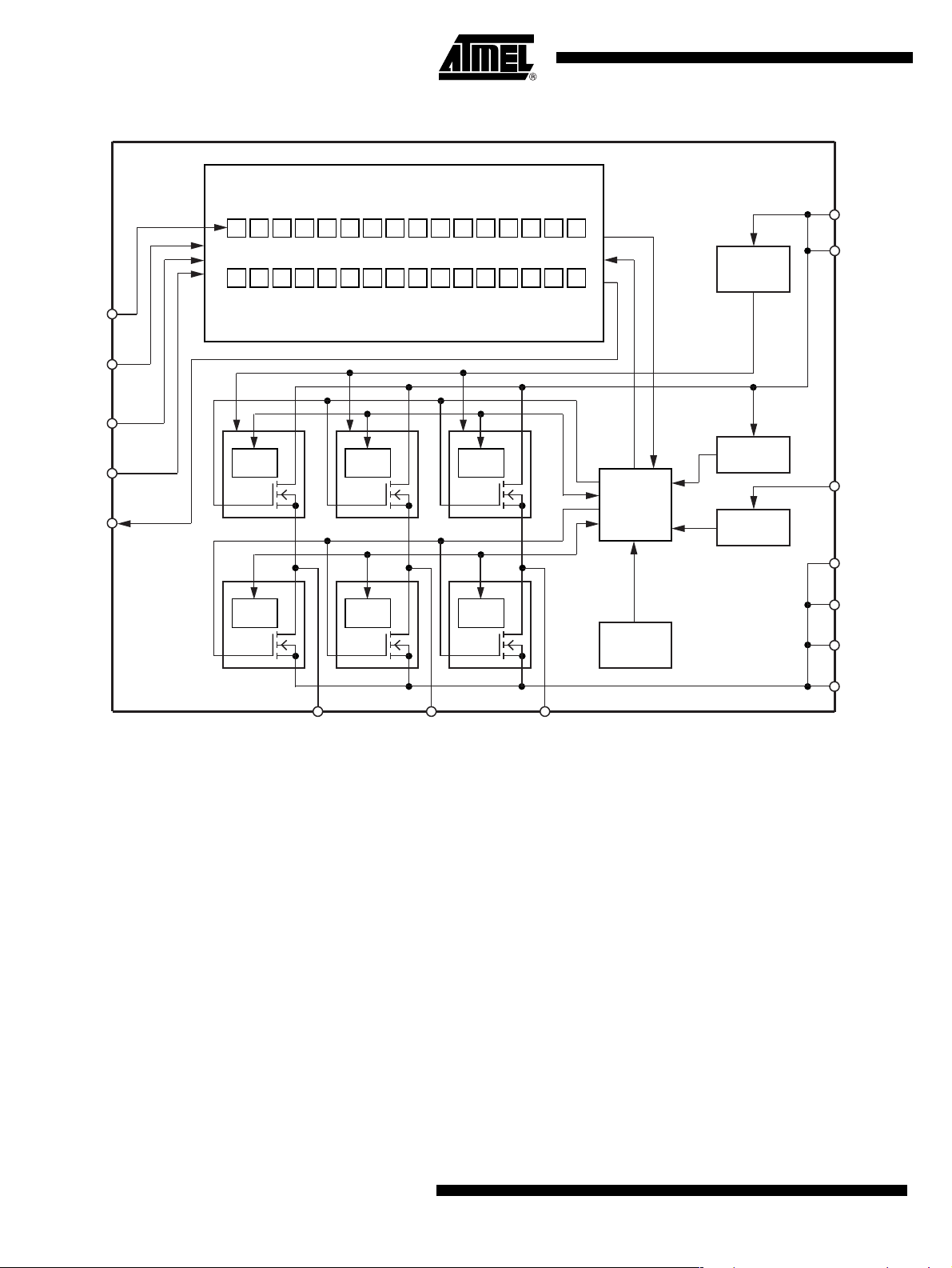
Figure 1-1. Block Diagram
n.u.n.
Input register
Ouput register
DI
4
CLK
5
CS
3
INH
8
DO
7
P
S
F
detector
detector
Faul t
Faul t
H
L
H
L
H
O
S
C
u.
O
S
P
C
L
D
1/2
n.u.n.
n.u.n.
n.u.n.u.n.u.n.
u.
n.u.n.
u.
Faul t
detector
Faul t
detector
OUT3
n.
u.
u.
12/13
L
S
S
3
u.
H
n.
S
u.
3
OUT2
S
S
2
2
3
Serial interface
L
H
L
S
S
S
3
2
2
Faul t
detector
Faul t
detector
15/16
S
S
S
R
1
1
R
Charge
pump
L
S
1
OUT1
T
P
Control
logic
Thermal
protection
UV
protection
Power on
reset
H
S
1
10
VS
11
VS
9
VCC
14
GND
17
GND
18
GND
6
GND
2
ATA6827 [Preliminary]
4912C–AUTO–10/06
Page 3
ATA6827 [Preliminary]
2. Pin Configuration
Figure 2-1. Pinning QFN18
PGND3
PGND1
OUT1S
OUT1F
PGND2
OUT2S
CS
DI
18 17 16 15 1314
1
2
3
4
5
6
OUT3S
OUT3
CLK
GND
Table 2-1. Pin Description
Pin Symbol Function
1 OUT3S Sense OUT3, internal connected to pin 2 via lead
2 OUT3 Half-bridge output 3
3 CS
4 DI
5 CLK
6 GND Ground; reference potential
7 DO
8 INH Inhibit input; 5-V logic input with internal pull down; low = standby, high = normal operation
9 VCC Logic supply voltage (5 V)
10 VS Power supply for output stages OUT1, OUT2 and OUT3, internal supply
11 VS Power supply for output stages OUT1, OUT2 and OUT3, internal supply
12 OUT2 Half-bridge output 2
13
OUT2S
14 PGND2 Power Ground OUT2
15 OUT1F Half-bridge output 1
16 OUT1S Sense OUT1, internal connected to pin 15 via lead
17
18
PGND1
PGND3
PGND1
PGND3
Chip select input; 5-V CMOS logic level input with internal pull up;
low = serial communication is enabled, high = disabled
Serial data input; 5-V CMOS logic level input with internal pull down; receives serial data from the control
device; DI expects a 16-bit control word with LSB being transferred first
Serial clock input; 5-V CMOS logic level input with internal pull down;
controls serial data input interface and internal shift register (f
Serial data output; 5-V CMOS logic level tri-state output for output (status) register data; sends 16-bit
status information to the microcontroller (LSB is transferred first); output will remain tri-stated unless
device is selected by CS = low, therefore, several ICs can operate on one data output line only.
Sense OUT2, internal connected to pin 12 via bond; OUT2 controlled loads have to be connected to pin
12 OUT2F
Power Ground OUT1 and OUT3
Power Ground OUT1 and OUT3
12
11
10
OUT2
VS
VS
VCC
9
INH
8
DO
7
= 2 MHz)
max
4912C–AUTO–10/06
3
Page 4
3. Functional Description
3.1 Serial Interface
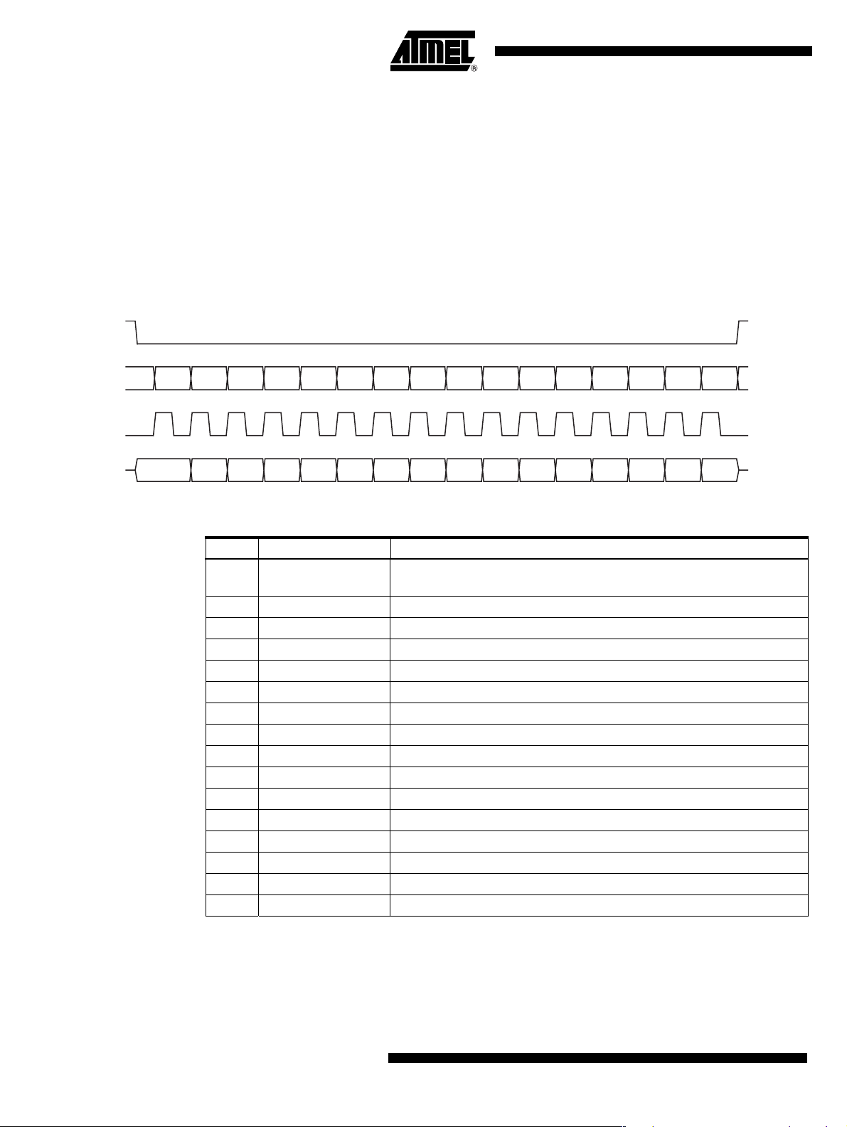
Data transfer starts with the falling edge of the CS signal. Data must appear at DI synchronized
to CLK and are accepted on the falling edge of the CLK signal. LSB (bit 0, SRR) has to be transferred first. Execution of new input data is enabled on the rising edge of the CS signal. When CS
is high, pin DO is in tri-state condition. This output is enabled on the falling edge of CS. Output
data will change their state with the rising edge of CLK and stay stable until the next rising edge
of CLK appears. LSB (bit 0, TP) is transferred first.
Figure 3-1. Data Transfer
CS
CLK
DO
DI
SRR LS1 HS1 LS2 HS2 LS3
0 1 2 3 4 5 6 7 8 9 10 11 12 13 14 15
TP S1L S1H S2L S2H S3L S3H n. u.
HS3
n. u.
n. u. n. u. n. u. n. u. n. u.
n. u. n. u. n. u. n. u. n. u. SCD OPL PSF
OCS
n. u. n. u.
Table 3-1. Input Data Protocol
Bit Input Register Function
0SRR
1
2
3
4
5
6
7
8
9
10
11
12
13
14
15
LS1 Controls output LS1 (high = switch output LS1 on)
HS1 Controls output HS1 (high = switch output HS1 on)
LS2 See LS1
HS2 See HS1
LS3 See LS1
HS3 See HS1
n. u. Not used
n. u. Not used
n. u. Not used
n. u. Not used
n. u. Not used
n. u. Not used
OCS Overcurrent shutdown (high = overcurrent shutdown is active)
n. u. Not used
n. u. Not used
Status register reset (high = reset; the bits PSF, OPL and SCD in the
output data register are set to low)
4
ATA6827 [Preliminary]
4912C–AUTO–10/06
Page 5
ATA6827 [Preliminary]
Table 3-2. Output Data Protocol
Output (Status)
Bit
0 TP Temperature prewarning: high = warning
1
2
3
4
5
6
7
8
9
10
11
12
13
14
15
Register Function
Status LS1 High = output is on, low = output is off; not affected by SRR
Status HS1 High = output is on, low = output is off; not affected by SRR
Status LS2 Description see LS1
Status HS2 Description see HS1
Status LS3 Description see LS1
Status HS3 Description see HS1
n. u. Not used
n. u. Not used
n. u. Not used
n. u. Not used
n. u. Not used
n. u. Not used
Short circuit detected: set high when at least one high-side or low-side
SCD
OPL
PSF Power-supply fail: undervoltage at pin VS detected
switch is switched off by a short-circuit condition. Bits 1 to 6 can be used
to detect the shorted switch.
Open load detected: set high, when at least one active high-side or
low-side switch sinks/sources a current below the open load threshold
current.
After power-on reset, the input register has the following status:
Bit 15 Bit 14 Bit 13
(OCS)
xxHxxxxxxLLLLLLL
Bit 12 Bit 11 Bit 10 Bit 9 Bit 8 Bit 7 Bit 6
(HS3)
Bit 5
(LS3)
Bit 4
(HS2)
Bit 3
(LS2)
Bit 2
(HS1)
Bit 1
(LS1)
Bit 0
(SRR)
The following patterns are used to enable internal test modes of the IC. It is not recommended to use these patterns during
normal operation.
Bit 15 Bit 14 Bit 13
(OCS)
HHHHHLLLLLLLLLLL
HHHLLHHLLLLLLLLL
HHHLLLLHHLLLLLLL
Bit 12 Bit 11 Bit 10 Bit 9 Bit 8 Bit 7 Bit 6
(HS3)
Bit 5
(LS3)
Bit 4
(HS2)
Bit 3
(LS2)
Bit 2
(HS1)
Bit 1
(LS1)
Bit 0
(SRR)
4912C–AUTO–10/06
5
Page 6

3.2 Power-supply Fail
In case of undervoltage at pin VS, the Power-Supply Fail bit (PSF) in the output register is set
and all outputs are disabled. To detect an undervoltage, its duration has to be longer than the
undervoltage detection delay time t
age recovers to a normal operating value. The PSF bit stays high until it is reset by the SRR
(Status Register Reset) bit in the input register.
3.3 Open-load Detection
If the current through a high-side or low-side switch in the ON-state stays below the open-load
detection threshold, the open-load detection bit (OPL) in the output register is set.
The OPL bit stays high until it is reset by the SRR bit in the input register. To detect an open
load, its duration has to be longer than the open-load detection delay time t
3.4 Overtemperature Protection
If the junction temperature of one or more output stages exceeds the thermal prewarning threshold, T
temperature falls below the thermal prewarning threshold, T
bit can be read without transferring a complete 16-bit data word. The status of TP is available at
pin DO with the falling edge of CS. After the microcontroller has read this information, CS is set
high and the data transfer is interrupted without affecting the status of input and output registers.
If the junction temperature of one or more output stages exceeds the thermal shutdown threshold, T
j switch off
low. The outputs can be enabled again when the temperature falls below the thermal shutdown
threshold, T
warning and shutdown threshold avoids oscillations.
, the temperature prewarning bit (TP) in the output register is set. When the
jPW set
, all outputs are disabled and the corresponding bits in the output register are set to
jswitch on
. The outputs are enabled immediately when supply volt-
dUV
.
dSd
jPW reset
, the bit TP is reset. The TP
and the SRR bit in the input register is set to high. Hysteresis of thermal pre-
3.5 Short-circuit Protection
The output currents are limited by a current regulator. Overcurrent detection is activated by writing a high to the OCS (Overcurrent Shutdown) bit in the input register. When the current in an
output stage exceeds the overcurrent limitation and shutdown threshold, it is switched off after a
delay time (t
the output register is set to low. For OCS = low the overcurrent shutdown is inactive. The SCD
bit is also set if the current exceeds the overcurrent limitation and shutdown threshold, but the
outputs are not affected. By writing a high to the SRR bit in the input register the SCD bit is reset
and the disabled outputs are enabled.
3.6 Inhibit
Applying 0V to pin 8 (INH) inhibits the ATA6827.
All output switches are then turned off and switched to tri-state. The data in the output register is
deleted. The output switches can be activated again by switching pin 8 (INH) to 5V which initiates an internal power-on reset.
). The short-circuit detection bit (SCD) is set and the corresponding status bit in
dSd
6
ATA6827 [Preliminary]
4912C–AUTO–10/06
Page 7
ATA6827 [Preliminary]
4. Absolute Maximum Ratings
Stresses beyond those listed under “Absolute Maximum Ratings” may cause permanent damage to the device. This is a stress rating
only and functional operation of the device at these or any other conditions beyond those indicated in the operational sections of this
specification is not implied. Exposure to absolute maximum rating conditions for extended periods may affect device reliability.
All values refer to GND pins.
Parameters Pin Symbol Value Unit
Supply voltage 10, 11 V
Supply voltage
t < 0.5s; I
> –2A
S
10, 11
Logic supply voltage 9 V
Logic input voltage 3, 4, 5, 8
VCS,VDI, V
Logic output voltage 7
Input current 3, 4, 5, 8
ICS, IDI, I
Output current 7
I
I
Out3
Out3
Out3
, I
, I
, I
Output current 2, 12, 15
Output voltage 2, 12, 15 I
Reverse conducting current
=150 µs)
(t
pulse
2, 12, 15
Junction temperature range
Storage temperature range
T
Ambient temperature range
VS
V
VS
VCC
, V
CLK
V
DO
CLK, IINH
I
DO
Out2, IOut1
Out2, IOut1
Out2, IOut1
T
j
STG
T
a
INH
Internally limited, see output specification
–0.3 to +40 V
–1 V
–0.3 to +7 V
–0.3 to V
–0.3 to V
+ 0.3 V
VCC
+ 0.3 V
VCC
–10 to +10 mA
–10 to +10 mA
–0.3 to +40 V
17 A
–40 to +200 °C
–55 to +200 °C
–40 to +150 °C
5. Thermal Resistance
Parameters Test Conditions Symbol Value Unit
Junction case R
Junction ambient
(1)
thjc
R
thJA
maximum 15 K/W
40 K/W
Notes: 1. Depends on PCB board design
6. Operating Range
Parameters Symbol Value Unit
(2)
V
Supply voltage V
Logic supply voltage V
Logic input voltage VCS,VDI, V
Serial interface clock frequency f
CLK
Junction temperature range T
Note: Threshold for undervoltage detection
VS
VCC
CLK, VINH
j
to 40 V
UV
4.75 to 5.25 V
–0.3 to V
VCC
2 MHz
–40 to +200 °C
V
4912C–AUTO–10/06
7
Page 8

7. Noise and Surge Immunity
Parameters Test Conditions Value
Conducted interferences ISO 7637-1 Level 4
(1)
Interference suppression VDE 0879 Part 2 Level 5
ESD (Human Body Model) ESD S 5.1 2 kV
CDM (Charged Device Model) ESD STM 5.3.1-1999 all pins 500V
Note: Test pulse 5: V
smax
= 40V
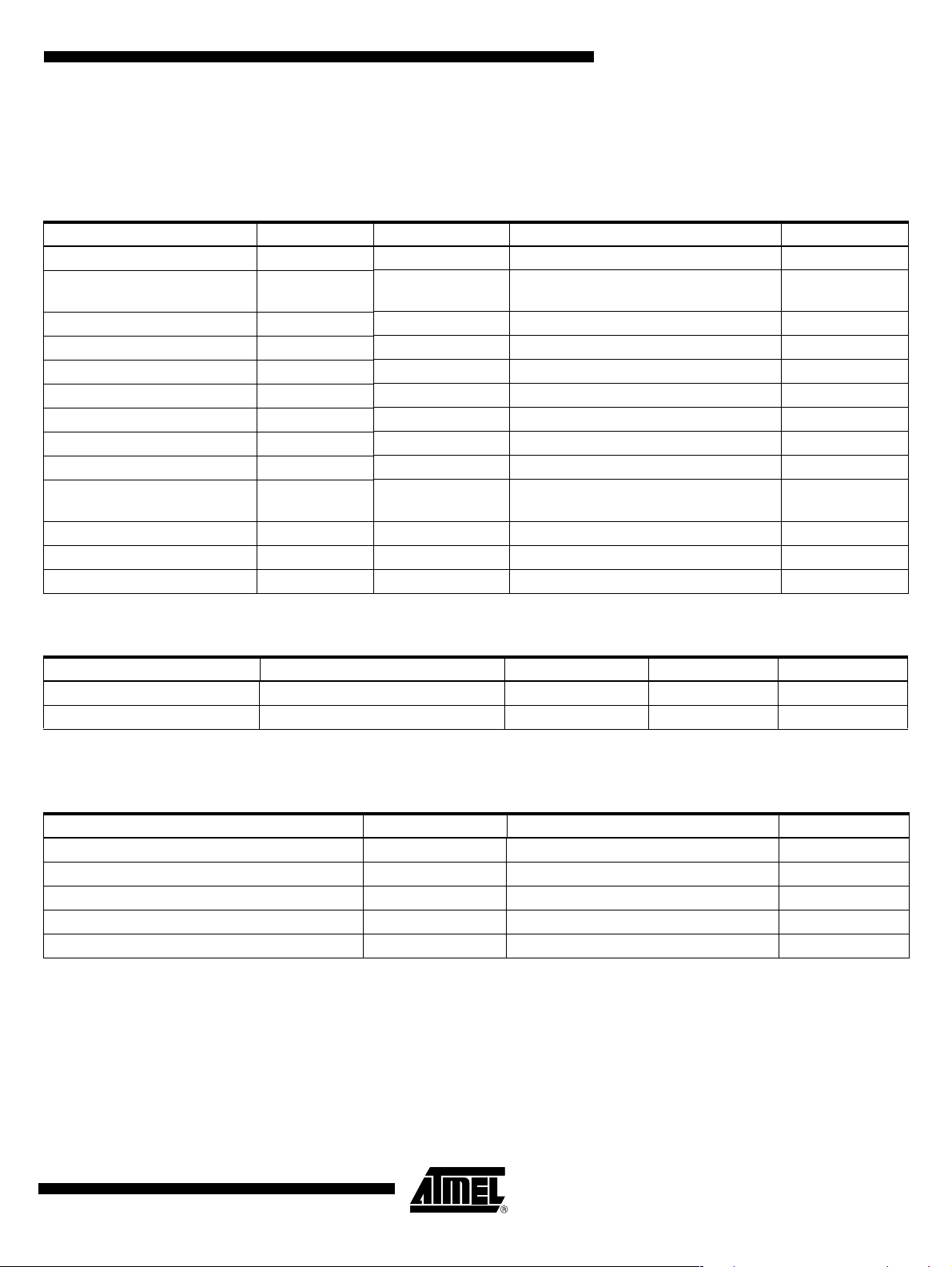
8. Electrical Characteristics
7.5V < VVS < 40V; 4.75V < V
GND pins.
No. Parameters Test Conditions Pin Symbol Min. Typ. Max. Unit Type*
1 Current Consumption
1.1 Quiescent current VS VVS < 20V, INH = low 10, 11 I
1.2 Quiescent current VCC
1.3 Supply current VS
1.4 Supply current VCC
1.5 Discharge current VS
1.6 Discharge current VS
2 Undervoltage Detection, Power-on Reset
Power-on reset
2.1
threshold
Power-on reset
2.2
delay time
Undervoltage-detection
2.3
threshold
Undervoltage-detection
2.4
hysteresis
Undervoltage-detection
2.5
delay time
3 Thermal Prewarning and Shutdown
3.1 Thermal prewarning set T
Thermal prewarning
3.2
reset
Thermal prewarning
3.3
hysteresis
3.4 Thermal shutdown off T
3.5 Thermal shutdown on T
*) Type means: A =100% tested, B = 100% correlation tested, C = Characterized on samples, D = Design parameter
Note: 1. Delay time between rising edge of the input signal at pin CS after data transmission and switch on output stages to 90% of
final level. Device not in standby for t > 1 ms
< 5.25 V; INH = High; –40°C ≤ Tj≤ 200°C; Ta≤ 150°C; unless otherwise specified, all values refer to
VCC
1 60 µA A
15 40 µA A
4 6 mA A
350 500 µA A
0.6 V A
15 °C B
4.75 V < V
INH = low
VVS< 20V normal
operating, all outputs off
4.75V < V
normal operating
VVS = 32.5V,
INH = low
VVS = 40V,
INH = low
< 5.25V,
VCC
< 5.25V,
VCC
9 I
10, 11 I
9 I
10, 11 I
10, 11 I
9 V
After switching on V
V
= 5V 10, 11 V
CC
V
= 5V 10, 11 ∆V
CC
CC
VS
VCC
VS
VCC
VS
VS
VCC
t
dPor
Uv
t
dUV
jPW set
T
jPW reset
∆T
jPW
j switch off
j switch on
0.5 5.5 mA A
2.0 10 mA A
3.1 3.9 4.5 V A
30 95 190 µs A
5.5 7.1 V A
Uv
10 40 µs A
170 195 220 °C B
155 180 205 °C B
200 225 250 °C B
185 210 235 °C B
8
ATA6827 [Preliminary]
4912C–AUTO–10/06
Page 9

ATA6827 [Preliminary]
8. Electrical Characteristics (Continued)
7.5V < VVS < 40V; 4.75V < V
GND pins.
No. Parameters Test Conditions Pin Symbol Min. Typ. Max. Unit Type*
Thermal shutdown
3.6
hysteresis
Ratio thermal shutdown
3.7
off/thermal prewarning
set
Ratio thermal shutdown
3.8
on/thermal prewarning
reset
4 Output Specification (OUT1-OUT3)
4.1
On resistance
4.2 I
High-side output
4.3
leakage current
Low-side output
4.4
leakage current
High-side switch
4.5
reverse diode forward
voltage
Low-side switch reverse
4.6
diode forward voltage
High-side overcurrent
4.7
limitation and shutdown
threshold
Low-side overcurrent
4.8
limitation and shutdown
threshold
High-side overcurrent
4.18
limitation and shutdown
threshold
Low-side overcurrent
limitation and shutdown
4.19
threshold
Overcurrent shutdown
4.9
delay time
High-side open-load
4.10
detection threshold
Low-side open-load
4.11
detection threshold
Open-load detection
4.12
delay time
*) Type means: A =100% tested, B = 100% correlation tested, C = Characterized on samples, D = Design parameter
Note: 1. Delay time between rising edge of the input signal at pin CS after data transmission and switch on output stages to 90% of
final level. Device not in standby for t > 1 ms
< 5.25 V; INH = High; –40°C ≤ Tj≤ 200°C; Ta≤ 150°C; unless otherwise specified, all values refer to
VCC
I
= –0.9A
Out 1-3
= +0.9A
Out 1-3
V
= 0V
Out 1-3
,
output stages off
V
= V
Out 1-3
VS,
output stages off
I
= 1.5A
Out 1-3
I
= –1.5A
Out 1-3
7.5V < VS < 20V
7.5V < VS < 20V
20V < VS < 40V
20V < VS < 40V
2, 12,
15
2, 12,
15
2, 12,
15
2, 12,
15
2, 12,
15
2, 12,
15
2, 12,
15
2, 12,
15
2, 12,
15
2, 12,
15
2, 12,
15
2, 12,
15
2, 12,
15
∆T
T
j switch off/
T
T
j switch on/
T
jPW reset
R
R
I
I
V
Out1-3
V
I
I
I
I
I
I
j switch off
jPW set
DSOn1-3
DSOn1-3
Out1-3
Out1-3
– V
Out 1-3
Out1-3
Out1-3
Out1-3
Out1-3
t
dSd
Out1-3
Out1-3
t
dSd
1.05 1.15 B
1.05 1.15 B
–60 µA A
VS
–2 V A
1.0 1.3 1.7 AA A
–1.7 –1.3 –1.0 A A
1.0 1.3 2.0 AA A
–2.0 –1.3 –1.0 A A
10 40 µs A
–55 –30 –5 mA A
5 30 55 mA A
200 600 µs A
15 °C B
1.8 Ω A
1.8 Ω A
300 µA A
2 V A
4912C–AUTO–10/06
9
Page 10

8. Electrical Characteristics (Continued)
7.5V < VVS < 40V; 4.75V < V
GND pins.
No. Parameters Test Conditions Pin Symbol Min. Typ. Max. Unit Type*
High-side output switch
4.13
on delay
Low-side output switch
4.14
on delay
High-side output switch
4.15
off delay
Low-side output switch
4.16
off delay
(1)
(1)
(1)
(1)
Dead time between
4.17
corresponding highand low-side switches
5 Logic Inputs DI, CLK, CS, INH
Input voltage low-level
5.1
threshold
Input voltage high-level
5.2
threshold
Hysteresis of input
5.3
voltage
Pull-down current pin
5.4
DI, CLK, INH
Pull-up current
5.5
Pin CS
6 Serial Interface – Logic Output DO
6.1 Output-voltage low level I
Output-voltage high
6.2
level
Leakage current
6.3
(tri-state)
7 Inhibit Input - Timing
Delay time from
7.1
standby to normal
operation
*) Type means: A =100% tested, B = 100% correlation tested, C = Characterized on samples, D = Design parameter
Note: 1. Delay time between rising edge of the input signal at pin CS after data transmission and switch on output stages to 90% of
final level. Device not in standby for t > 1 ms
< 5.25 V; INH = High; –40°C ≤ Tj≤ 200°C; Ta≤ 150°C; unless otherwise specified, all values refer to
VCC
VVS = 13V
R
= 30Ω
Load
VVS = 13V
= 30Ω
R
Load
VVS = 13V
R
= 30Ω
Load
VVS = 13V
R
= 30Ω
Load
VVS = 13V
R
= 30Ω
Load
3, 4, 5,
8
3, 4, 5,
8
3, 4, 5,
8
VDI, V
CLK, VINH
= V
CC
4, 5, 8 I
VCS= 0V 3 I
= 2 mA 7 V
DOL
I
= –2 mA 7 V
DOL
V
= V
CS
0V < V
CC
DO
< V
VCC
7 I
t
don
t
don
t
doff
t
doff
t
don
– t
V
V
∆V
DOH
t
dINH
doff
IL
IH
I
PD
PU
DOL
DO
1 µs A
0.3 ×
V
VCC
50 700 mV B
5 70 µA A
–70 –5 µA A
V
VCC
–0.7V
–15 +15 µA A
20 µs A
20 µs A
20 µs A
3µsA
V A
0.7 ×
V
VCC
V A
0.4 V A
V A
100 µs A
10
ATA6827 [Preliminary]
4912C–AUTO–10/06
Page 11

ATA6827 [Preliminary]
9. Serial Interface – Timing
No. Parameters Test Conditions Pin Timing Chart No.
DO enable after CS
8.1
falling edge
DO disable after CS
8.2
rising edge
= 100 pF 7 1 t
C
DO
= 100 pF 7 2 t
C
DO
8.3 DO fall time CDO = 100 pF 7 - t
8.4 DO rise time C
8.5 DO valid time C
= 100 pF 7 - t
DO
= 100 pF 7 10 t
DO
8.6 CS setup time 3 4 t
8.7 CS setup time 3 8 t
8.8 CS high time 3 9 t
8.9 CLK high time 5 5 t
8.10 CLK low time 5 6 t
8.11 CLK period time 5 - t
8.12 CLK setup time 5 7 t
8.13 CLK setup time 5 3 t
8.14 DI setup time 4 11 t
8.15 DI hold time 4 12 t
*) Type means: A =100% tested, B = 100% correlation tested, C = Characterized on samples, D = Design parameter
Note: 1. Serial Interface Timing with Chart Numbers
(1)
Symbol Min. Typ. Max. Unit Type*
ENDO
DISDO
DOf
DOr
DOVal
CSSethl
CSSetlh
CSh
CLKh
CLKl
CLKp
CLKSethl
CLKSetlh
DIset
DIHold
225 ns D
225 ns D
500 ns D
225 ns D
225 ns D
500 ns D
225 ns D
225 ns D
40 ns D
40 ns D
200 ns D
200 ns D
100 ns D
100 ns D
200 ns D
4912C–AUTO–10/06
11
Page 12

Figure 9-1. Serial Interface Timing with Chart Numbers
CS
CLK
1
2
CS
DO
9
4
5
3
6 8
7
DI
11
CLK
10 12
DO
Inputs DI, CLK, CS: High level = 0.7 × VCC, low level = 0.3 × V
Output DO: High level = 0.8 × VCC, low level = 0.2 × V
CC
CC
12
ATA6827 [Preliminary]
4912C–AUTO–10/06
Page 13

10. Application Circuit
Figure 10-1. Application Circuit
V
CC
Reset
V
Enable
Trigger
DI
4
CLK
5
CS
3
INH
8
DO
7
CC
U5021M
Watchdog
Micro-
controller
O
S
n.u.n.
C
u.
Input register
Ouput register
O
S
P
P
C
S
L
D
F
Fault
detector
Fault
detector
n.u.n.
n.u.n.
2
n.u.n.u.n.u.n.
u.
n.u.n.
u.
Fault
detector
Fault
detector
OUT3
ATA6827 [Preliminary]
V
VS
VS
VCC
GND
GND
GND
GND
S
BYT41D
+
V
Batt
13V
V
CC
V
CC
5V
+
H
L
H
L
H
L
S
S
3
u.
H
n.
n.
S
u.
u.
u.
3
12
OUT2
S
S
2
2
3
Serial interface
H
L
L
S
S
S
2
2
3
Fault
detector
Fault
detector
S
S
S
R
1
1
R
Charge
pump
H
L
T
S
S
P
1
1
UV
protection
Control
logic
Thermal
protection
15
OUT1
Power on
reset
10
11
9
14
17
18
6
11. Application Notes
It is strongly recommended to connect the blocking capacitors at VCC and VS as close as possible to the power supply and GND pins.
Recommended value for capacitors at V
Electrolytic capacitor C > 22 µF in parallel with a ceramic capacitor C = 100 nF. The value for
electrolytic capacitor depends on external loads, conducted interferences and reverse conducting current I
Recommended value for capacitors at V
Electrolytic capacitor C > 10 µF in parallel with a ceramic capacitor C = 100 nF.
To reduce thermal resistance it is recommended to place cooling areas on the PCB as close as
possible to the GND pins and to the die pad.
4912C–AUTO–10/06
MM
:
S
(see Section 4. ”Absolute Maximum Ratings” on page 7).
Out1,2,3
:
CC
13
Page 14

12. Ordering Information
Extended Type Number Package Remarks
ATA6827-PIQW QFN18, 4 mm × 4 mm Taped and reeled, Pb-free
13. Package Information
Package: VQFN_4 x 4_18L
Exposed pad 2.5 x 3.125
Dimensions in mm
Not indicated tolerances ±0.05
Top
18
1
Pin 1 identification
6
Drawing-No.: 6.543-5133.01-4
Issue: preliminary copy; 06.10.06
Bottom
2.5
Z
13 18
12
3.125±0.15
4
0.2
±0.1
0.9
Z 10:1
0.23±0.07
7
2.6
technical drawings
according to DIN
specifications
0.45±0.1
0.5 nom.
1
2.5
6
±0.15
14
ATA6827 [Preliminary]
4912C–AUTO–10/06
Page 15

Atmel Corporation Atmel Operations
2325 Orchard Parkway
San Jose, CA 95131, USA
Tel: 1(408) 441-0311
Fax: 1(408) 487-2600
Regional Headquarters
Europe
Atmel Sarl
Route des Arsenaux 41
Case Postale 80
CH-1705 Fribourg
Switzerland
Tel: (41) 26-426-5555
Fax: (41) 26-426-5500
Asia
Room 1219
Chinachem Golden Plaza
77 Mody Road Tsimshatsui
East Kowloon
Hong Kong
Tel: (852) 2721-9778
Fax: (852) 2722-1369
Japan
9F, Tonetsu Shinkawa Bldg.
1-24-8 Shinkawa
Chuo-ku, Tokyo 104-0033
Japan
Tel: (81) 3-3523-3551
Fax: (81) 3-3523-7581
Memory
2325 Orchard Parkway
San Jose, CA 95131, USA
Tel: 1(408) 441-0311
Fax: 1(408) 436-4314
Microcontrollers
2325 Orchard Parkway
San Jose, CA 95131, USA
Tel: 1(408) 441-0311
Fax: 1(408) 436-4314
La Chantrerie
BP 70602
44306 Nantes Cedex 3, France
Tel: (33) 2-40-18-18-18
Fax: (33) 2-40-18-19-60
ASIC/ASSP/Smart Cards
Zone Industrielle
13106 Rousset Cedex, France
Tel: (33) 4-42-53-60-00
Fax: (33) 4-42-53-60-01
1150 East Cheyenne Mtn. Blvd.
Colorado Springs, CO 80906, USA
Tel: 1(719) 576-3300
Fax: 1(719) 540-1759
Scottish Enterprise Technology Park
Maxwell Building
East Kilbride G75 0QR, Scotland
Tel: (44) 1355-803-000
Fax: (44) 1355-242-743
RF/Automotive
Theresienstrasse 2
Postfach 3535
74025 Heilbronn, Germany
Tel: (49) 71-31-67-0
Fax: (49) 71-31-67-2340
1150 East Cheyenne Mtn. Blvd.
Colorado Springs, CO 80906, USA
Tel: 1(719) 576-3300
Fax: 1(719) 540-1759
Biometrics/Imaging/Hi-Rel MPU/
High-Speed Converters/RF Datacom
Avenue de Rochepleine
BP 123
38521 Saint-Egreve Cedex, France
Tel: (33) 4-76-58-30-00
Fax: (33) 4-76-58-34-80
Literature Requests
www.atmel.com/literature
Disclaimer: The information in this document is provided in connection with Atmel products. No license, express or implied, by estoppel or otherwise, to any
intellectual property right is granted by this document or in connection with the sale of Atmel products. EXCEPT AS SET FORTH IN ATMEL’S TERMS AND CONDI-
TIONS OF SALE LOCATED ON ATMEL’S WEB SITE, ATMEL ASSUMES NO LIABILITY WHATSOEVER AND DISCLAIMS ANY EXPRESS, IMPLIED OR STATUTORY
WARRANTY RELATING TO ITS PRODUCTS INCLUDING, BUT NOT LIMITED TO, THE IMPLIED WARRANTY OF MERCHANTABILITY, FITNESS FOR A PARTICULAR
PURPOSE, OR NON-INFRINGEMENT. IN NO EVENT SHALL ATMEL BE LIABLE FOR ANY DIRECT, INDIRECT, CONSEQUENTIAL, PUNITIVE, SPECIAL OR INCIDENTAL DAMAGES (INCLUDING, WITHOUT LIMITATION, DAMAGES FOR LOSS OF PROFITS, BUSINESS INTERRUPTION, OR LOSS OF INFORMATION) ARISING OUT
OF THE USE OR INABILITY TO USE THIS DOCUMENT, EVEN IF ATMEL HAS BEEN ADVISED OF THE POSSIBILITY OF SUCH DAMAGES. Atmel makes no
representations or warranties with respect to the accuracy or completeness of the contents of this document and reserves the right to make changes to specifications
and product descriptions at any time without notice. Atmel does not make any commitment to update the information contained herein. Unless specifically provided
otherwise, Atmel products are not suitable for, and shall not be used in, automotive applications. Atmel’s products are not intended, authorized, or warranted for use
as components in applications intended to support or sustain life.
© 2006 Atmel Corporation. All rights reserved. Atmel®, logo and combinations thereof, Everywhere You Are® and others are registered trade-
marks or trademarks of Atmel Corporation or its subsidiaries. Other terms and product names may be trademarks of others.
4912C–AUTO–10/06
 Loading...