

Page 1

Features
• PWM and Direction-controlled Driving of Four Externally-powered NMOS Transistors
• A Programmable Dead Time Is Included to Avoid Peak Currents Within the H-bridge
• Integrated Charge Pump to Provide Gate Voltages for High-side Drivers and to Supply
the Gate of the External Battery Reverse Protection NMOS
• 5V/3.3V Regulator and Current Limitation Function
• Reset Derived From 5V/3.3V Regulator Output Voltage
• Sleep Mode With Supply Current of Typically < 45 µA, Wake-up by Signal on Pins EN2
or on LIN Interface
• A Programmable Window Watchdog
• Battery Overvoltage Protection and Battery Undervoltage Management
• Overtemperature Warning and Protection (Shutdown)
• LIN 2.0 Compliant
• 3.3V/5V Regulator with Trimmed Band Gap
• QFN32 Package
1. Description
The ATA6823 is designed for several body and powertrain applications. The IC is
used to drive a continuous current motor in a full H-bridge configuration. An external
microcontroller controls the driving function of the IC by providing a PWM signal and a
direction signal and allows the use of the IC in a motor-control application. The PWM
control is performed by the low-side switch; the high-side switch is permanently on in
the driving phase. The VMODE configuration pin can be set to 5V or 3.3V mode (for
regulator and interface high level). The window watchdog has a programmable time,
programmable by choosing a certain value of the external watchdog resistor RWD,
internally trimmed to an accuracy of 10%. For communication a LIN transceiver 2.0 is
integrated.
H-bridge Motor
Driver
ATA6823
Preliminary
4856E–AUTO–07/07
Page 2
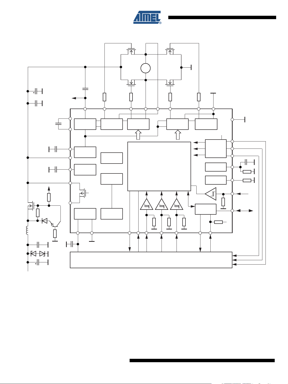
Figure 1-1. Block Diagram
M
CP
VRES H2
CPLO
Charge
Pump
CPIH
VG
PBAT
VBAT
CP
VINT
VBAT
VBATSW
12V
Regulator
Vint 5V
Regulator
VCC 5V
Regulator
VCC
R
GATE
HS Driver 2
OTP
12 bit
Oscillator
VBG
Bandgap
VMODE /RESET
R
GATE
H1
HS Driver 1
Logic Control
EN1
WD
S1 S2 L2
DIR
R
GATE
LS Driver 1
PWM
R
GATE
LS Driver 2
OT
UV
Supervisor
OV
CC timer
WD timer
LIN
TXRX
PGNDL1
VBAT
VCC
GND
DG3
DG2
DG1
CC
EN2
LIN
Microcontroller
Battery
2
ATA6823 [Preliminary]
4856E–AUTO–07/07
Page 3
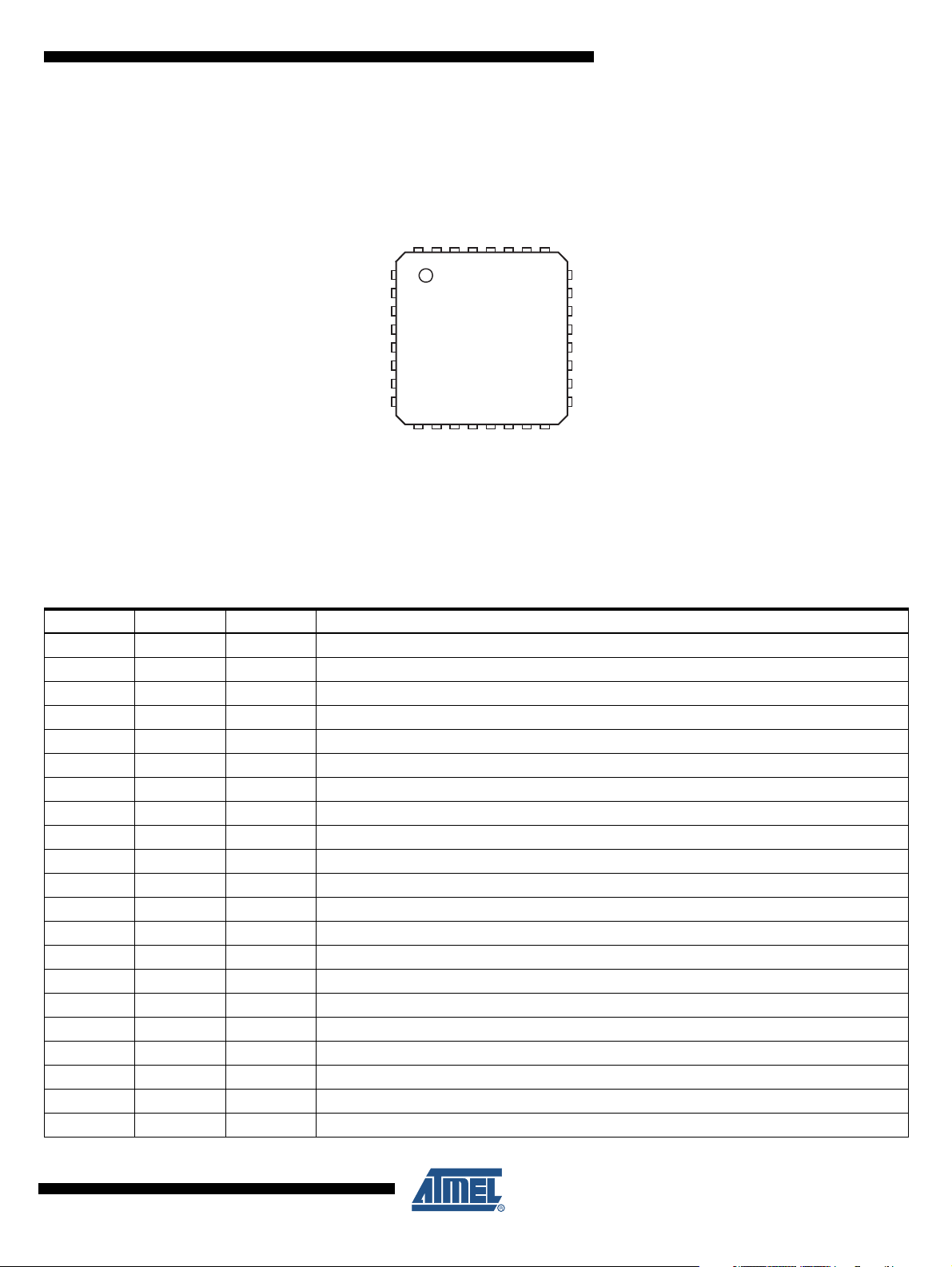
2. Pin Configuration
/
Figure 2-1. Pinning QFN32
VMODE
VINT
RWD
CC
RESET
WD
GND
LIN
EN2
VBATSW
VBAT
VCC
PGNDL1L2
32 31 30 29 28 27 26 25
1
2
3
Atmel YWW
4
5
6
7
8
ATA6823
ZZZZZ-AL
9 10 11 12 13 14 15 16
PBAT
24
23
22
21
20
19
18
17
ATA6823 [Preliminary]
VG
CPLO
CPHI
VRES
H2
S2
H1
S1
Table 2-1. Pin Description
Pin Symbol I/O Function
1 VMODE I Selector for V
2 VINT I/O Blocking capacitor 220 nF/10V/X7R
3 RWD I Resistor defining the watchdog interval
4 CC I/O RC combination to adjust cross conduction time
5 /RESET O Reset signal for microcontroller
6 WD I Watchdog trigger signal
7 GND I Ground for chip core
8 LIN I/O LIN-bus terminal
9 TX I Transmit signal to LIN bus from microcontroller
10 DIR I Defines the rotation direction for the motor
11 PWM I PWM input controls motor speed
12 EN1 I Microcontroller output to keep the chip in Active mode
13 RX O Receive signal from LIN bus for microcontroller
14 DG3 O Diagnostic output 3
15 DG2 O Diagnostic output 2
16 DG1 O Diagnostic output 1
17 S1 I/O Source voltage H-bridge, high-side 1
18 H1 O Gate voltage H-bridge, high-side 1
19 S2 I/O Source voltage H-bridge, high-side 2
20 H2 O Gate voltage H-bridge, high-side 2
21 VRES I/O Gate voltage for reverse protection NMOS, blocking capacitor 470 nF/25V/X7R
TX
DIR
EN1
PWM
RX
DG3
DG2
DG1
Note: YWW Date code (Y = Year - above 2000, WW = week number)
ATA6823 Product name
ZZZZZ Wafer lot number
AL Assembly sub-lot number
and interface logic voltage level
CC
4856E–AUTO–07/07
3
Page 4
Table 2-1. Pin Description (Continued)
Pin Symbol I/O Function
22 CPHI I
23 CPLO O
24 VG I/O Blocking capacitor 470 nF/25V/X7R
25 PBAT I Power supply (after reverse protection) for charge pump and H-bridge
26 L2 O Gate voltage H-bridge, low-side 2
27 L1 O Gate voltage H-bridge, low-side 1
28 PGND I Power ground for H-bridge and charge pump
29 VCC O 5V/100 mA supply for microcontroller, blocking capacitor 2.2 µF/10V/X7R
30 VBAT I Supply voltage for IC core (after reverse protection)
31 VBATSW O 100Ω PMOS switch from V
32 EN2 I Enable input
Charge pump capacitor 220 nF/25V/X7R
BAT
3. General Statement and Conventions
• Parameter values given without tolerances are indicative only and not to be tested in
production
• Parameters given with tolerances but without a parameter number in the first column of
parameter table are “guaranteed by design” (mainly covered by measurement of other
specified parameters). These parameters are not to be tested in production. The tolerances
are given if the knowledge of the parameter tolerances is important for the application
• The lowest power supply voltage is named GND
• All voltage specifications are referred to GND if not otherwise stated
• Sinking current means that the current is flowing into the pin (value is positive)
• Sourcing current means that the current is flowing out of the pin (value is negative)
3.1 Related Documents
• Qualification of integrated circuits according to Atmel® HNO procedure based on AEC-Q100
• AEC-Q100-004 and JESD78 (Latch-up)
• ESD STM 5.1-1998
• CEI 801-2 (only for information regarding ESD requirements of the PCB)
4
ATA6823 [Preliminary]
4856E–AUTO–07/07
Page 5
4. Application
4.1 General Remark
This chapter describes the principal application for which the ATA6823 was designed. Because
Atmel cannot be considered to understand fully all aspects of the system, application and environment, no warranties of fitness for a particular purpose are given.
Table 4-1. Typical External Components
ATA6823 [Preliminary]
Component Function Value Tolerance
C
C
C
R
C
C
C
R
C
VINT
VCC
CC
CC
VG
CP
VRES
RWD
LIN
Blocking capacitor at VINT 220 nF, 10V, X7R 10%
Blocking capacitor at VCC 2.2 µF, 10V, X7R 10%
Cross conduction time definition capacitor Typical 330 pF, 100V, COG
Cross conduction time definition resistor Typical 10 kΩ
Blocking capacitor at VG 470 nF, 25V, X7R 10%
Charge pump capacitor 220 nF, 25V, X7R 10%
Reservoir capacitor 470 nF, 25V, X7R 10%
Watchdog time definition resistor Typical 51 kΩ 1%
Filter capacitor for LIN bus Typical 220 pF, 100V 10%
5. Functional Description
5.1 Power Supply Unit with Supervisor Functions
5.1.1 Power Supply
The IC is supplied by a reverse-protected battery voltage. To prevent it from destruction, proper
external protection circuitry has to be added. It is recommended to use at least a capacitor combination of storage and HF caps behind the reverse protection circuitry and closed to the VBAT
pin of the IC (see Figure 1-1 on page 2).
A fully-internal low-power and low-drop regulator, stabilized by an external blocking capacitor
provides the necessary low-voltage supply needed for the wake-up process. The low-power
band gap reference is trimmed and is used for the bigger VCC regulator, too. All internal blocks
are supplied by the internal regulator.
Note: The internal supply voltage V
Nothing inside the IC except the logic interface to the microcontroller is supplied by the 5V/3.3V
VCC regulator.
A power-good comparator checks the output voltage of the V
chip in reset as long as the voltage is too low.
There is a high-voltage switch which brings out the battery voltage to the pin VBATSW for measurement purposes. This switch is switched ON for VCC = HIGH and stays ON in case of a
watchdog reset going to sleep mode, VBATSW turns OFF. The signal can be used to switch on
external voltage regulators, etc.
must not be used for any other supply purpose!
INT
regulator and keeps the whole
INT
4856E–AUTO–07/07
5
Page 6

5.1.2 Voltage Supervisor
This block is intended to protect the IC and the external power MOS transistors against overvoltage on battery level and to manage undervoltage on it.
Function: in case of both overvoltage alarm (V
nal NMOS motor bridge transistors will be switched off. The failure state will be flagged via DG2.
No other actions will be carried out. The voltage supervision block is connected to VBAT and filtered by a first-order low pass with a corner frequency of typical 15 kHz.
5.1.3 Temperature Supervisor
There is a temperature sensor integrated on-chip to prevent the IC from overheating due to a
failure in the external circuitry and to protect the external NMOSFET transistors.
In case of detected overtemperature (150°C), the diagnostic pin DG3 will be switched to “H” to
signalize this event to the microcontroller. It should undertake actions to reduce the power dissipation in the IC. In case of detected overtemperature (165°C), the V
including the LIN transceiver will be switched OFF immediately and /RESET will go LOW.
Both temperature thresholds are correlated. The absolute tolerance is ±10°C and there is a
built-in hysteresis of about 10°C to avoid fast oscillations. After cooling down below the 155°C
threshold; the IC will go into Active mode.
The LIN interface has a separate thermal shutdown with disabled the low-side driver at typically
165°C.
5.2 Sleep Mode
To be able to guarantee the low quiescent current of the inactive IC, a Sleep mode is established. In Sleep mode it is possible to wake-up the IC by using the pins EN2 or LIN. In Sleep
mode, the following blocks are active:
) and of undervoltage alarm (V
THOV
CC
) the exter-
THUV
regulator and all drivers
• Band gap
• Internal 5V regulator (VINT) with external blocking capacitor of 220 nF
• Input structure for detecting the EN2 pins threshold
• Wake-up block of the LIN receive part
5.3 Wake-up and Sleep Mode Strategy
The IC has two modes: Sleep and Active. The change between the modes is described below.
The default state after power-on is Active mode.
The wake-up procedure brings the IC from a standby mode (Sleep) to an active mode (Active).
The internal 5V supply VINT, the EN2 pin input structure and a certain part of the LIN receiver
are permanently active to ensure a proper startup of the system.
The Go to Active and Go to Sleep procedures are implemented as follows:
• Go to Active by activating pin EN2
The input EN2 is intended as a switch-on pin from an external signal. Its input structure consists
of a comparator with built-in hysteresis. It is ESD-protected by diodes against GND and V
this reason the input voltage level must be positive and not higher than V
BAT
; for
BAT
.
6
ATA6823 [Preliminary]
4856E–AUTO–07/07
Page 7

ATA6823 [Preliminary]
Pulling the EN2 pin up to the V
level will drive the IC into Active mode. EN2 is debounced with
BAT
a time constant of 20 µs, based on a 100 kHz clock.
• Go to Active using the LIN interface
The second possibility for wake-up can be performed using the LIN transceiver. In Sleep mode,
the LIN receiver is partially active.
The wake-up by LIN requires 2 steps:
1. If the voltage on pin LIN is below a value of V
/DATwake
(about V
– 2V) the receive part
VBAT
of the LIN interface is active (not to be confused with Active mode of the whole IC). The
active receive part is able to detect a valid LOW on the LIN pin.
2. If LIN = LOW during a filter time t
(typically 70 µs) the IC will change to Active
wakeLIN
mode. A short change back to HIGH during the filter time will reset the filter. This information is stored in a latch after entering Active mode
If the change to Active mode was caused by LIN, the EN1 or EN2 pins may remain LOW without
disturbing the Active mode.
• Stay in Active via EN1
The input EN1 is intended to keep the IC in Active Mode via a signal from the microcontroller.
The input is ESD-protected by diodes against GND and VCC. Therefore, the input voltage must
be positive and not higher than V
the VCC regulator is off in the Sleep mode and V
. EN1 cannot be used to switch from Sleep to Active because
CC
will be zero.
CC
• Go to Sleep
A HIGH to LOW transition at pin EN1 and a following permanent LOW for the time t
gotosleep
(typically 20 µs) switches the IC to Sleep mode.
Figure 5-1 illustrates the wake-up by LIN. The status PREWAKE is characterized by the acti-
vated receive block of the LIN interface. After going to Active mode, the V
regulator starts
CC
working.
Go to Sleep is possible with a valid HIGH to LOW transition at pin EN1 (permanent LOW for
longer than t
) if EN1 was in a valid HIGH state (HIGH for longer than tdb) before.
db
4856E–AUTO–07/07
7
Page 8
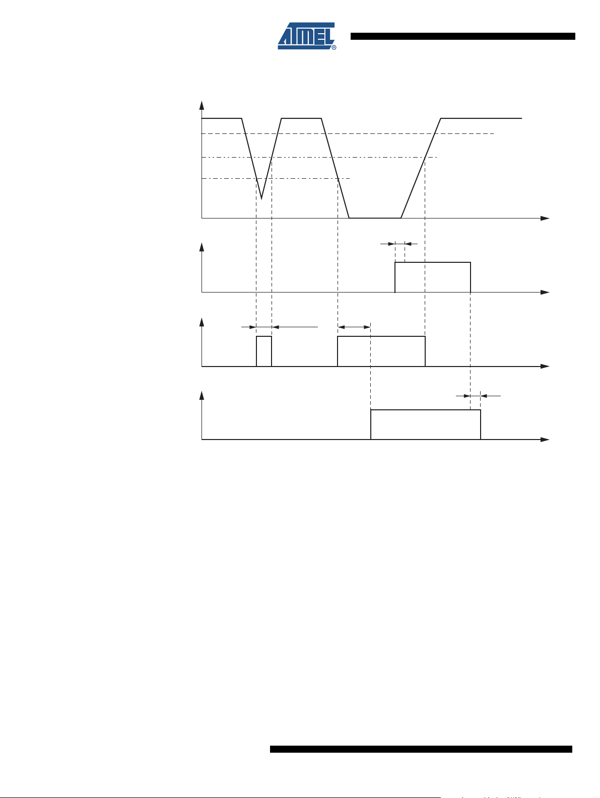
Figure 5-1. Wake-up by pin LIN
LIN
VBAT
EN1
RX
t < t
wake LIN
45% VBAT
t
wake LIN
VBAT - 1.5V
activating
55% VBAT
"PREWAKE"
t
t
db
t
STATUS
ACTIVE
SLEEP
t
t
db
t
8
ATA6823 [Preliminary]
4856E–AUTO–07/07
Page 9
5.4 5V/3.3V VCC Regulator
/
The 5V/3.3V regulator is fully integrated on-chip. It requires only a 2.2 µF ceramic capacitor for
stability and has 100 mA current capability. Using the VMODE pin, the output voltage can be
selected to either 5V or 3.3V. Switching of the output voltage during operation is not intended to
be supported. The VMODE pin must be hard-wired to either VINT for 5V or to GND for 3.3V. The
logic HIGH level of the microcontroller interface will be adapted to the VCC regulator voltage.
ATA6823 [Preliminary]
The output voltage accuracy is in general < ±3%; in the 5V mode with V
<5%.
To prevent destruction of the IC, the current delivered by the regulator is limited to maximum
160 mA to 320 mA. The delivered voltage will break down and a reset may occur.
Please note that this regulator is the main heat source on the chip. The maximum output current
at maximum battery voltage and high ambient temperature can only guaranteed if the IC is
mounted on an efficient heat sink.
A power-good comparator checks the output voltage of the VCC regulator and keeps the external microcontroller in reset as long as the voltage is too low.
5.5 Reset and Watchdog Management
The timing basis of the watchdog is provided by the trimmed internal oscillator. Its period T
adjustable via the external resistor R
The watchdog expects a triggering signal (a rising edge) from the microcontroller at the WD
input within a period time window of T
switched off during Sleep mode.
Figure 5-2. Timing Diagram of the Watchdog Function
res
< 8V it is limited to
VBAT
.
WD
. In order to save current consumption, the watchdog is
WD
t
resshortt
OSC
is
RESET
WD
5.5.1 Timing Sequence
4856E–AUTO–07/07
t
d
t
1
t
2
For example, with an external resistor R
of the watchdog.
T
= 12.32 µs, t1= 12.1 ms, t2= 9.61 ms, TWD= 16.88 ms ±10%
OSC
The times t
= 68 ms and td= 68 ms are fixed values with a tolerance of 10%.
res
t
d
t
1
=33kΩ ±1% we get the following typical parameters
WD
t
2
9
Page 10

After ramp-up of the battery voltage (power-on reset), the VCC regulator is switched on. The
0
reset output, /RESET, stays low for the time t
initial lead time t
(typically 68 ms for setups in the controller) the watchdog waits for a rising
d
(typically 68 ms), then switches to high. For an
res
edge on WD to start its normal window watchdog sequence. If no rising edge is detected, the
watchdog will reset the microcontroller for t
Times t
(close window) and t2 (open window) form the window watchdog sequence. To avoid
1
and wait td for the rising edge on WD.
res
receiving a reset from the watchdog, the triggering signal from the microcontroller must hit the
timeframe of t
= 9.61 ms. The trigger event will restart the watchdog sequence.
2
Figure 5-3. T
versus RWD
WD
60
50
40
30
TWD (ms)
20
10
max
min
0
10 20 30 40 50 60 70 80 90 10
RWD (kΩ)
typ
If triggering fails, /RESET will be pulled to ground for a shortened reset time of typically 2 ms.
The watchdog start sequence is similar to the power-on reset.
The internal oscillator is trimmed to a tolerance of < ±10%. This means that t
and t2 can also
1
vary by ±10%. The following calculation shows the worst case calculation of the watchdog
period T
t
= 0.90 × t1 = 10.87 ms, t
1min
t
= 0.90 × t2 = 8.65ms, t
2min
T
wdmax
T
wdmin
T
= 16.42 ms ±3.15 ms (±19.1%)
wd
Figure 5-3 above shows the typical watchdog period T
resistor R
A reset will be active for V
which the microcontroller has to provide.
wd
= 1.10 × t1 = 13.28 ms
1max
= 1.10 × t2 = 10.57 ms
2max
= t
+ t
= 10.87 ms + 8.65 ms = 19.52 ms
2min
= 13.28 ms
.
CC
< V
tHRESx
; the level V
= t
1min
1max
OSC
depending on the value of the external
WD
is realized with a hysteresis (HYS
tHRESx
RESth
).
5.6 LIN Transceiver
10
ATA6823 [Preliminary]
A bi-directional bus interface is implemented for data transfer between the LIN bus and the local
LIN protocol controller.
The transceiver consists of a low side driver (1.2V at 40 mA) with slew rate control, wave shaping, current limitation, and a high-voltage comparator followed by a debouncing unit in the
receiver.
4856E–AUTO–07/07
Page 11

5.6.1 Transmit Mode
During transmission, the data at the pin TX will be transferred to the bus driver to generate a bus
signal on pin LIN.
To minimize the electromagnetic emission of the bus line, the bus driver has an integrated slew
rate control and wave-shaping unit. Transmission will be interrupted in the following cases:
• Thermal shutdown active or overtemperature LIN active
• Sleep mode
Figure 5-4. Definition of Bus Timing Parameters
ATA6823 [Preliminary]
TXD
(input to transmitting Node)
TH
Rec(max)
V
S
(Transceiver
supply
of transmitting
node)
TH
TH
TH
Dom(max)
Rec(min)
Dom(min)
RXD
(output of receiving Node 1)
RXD
(output of receiving Node 2)
t
Bit
LIN Bus Signal
t
rx_pdf(1)
t
Bus_dom(max)
t
Bus_dom(min)
t
Bit
t
Bus_rec(min)
t
Bit
Thresholds of
receiving node 1
Thresholds of
receiving node 2
t
Bus_rec(max)
t
rx_pdr(1)
t
rx_pdr(2)
t
rx_pdf(2)
The recessive BUS level is generated from the integrated 30 kΩ pull-up resistor in series with an
active diode. This diode prevents the reverse current of VBUS during differential voltage
between VSUP and BUS (V
No additional termination resistor is necessary to use the ATA6823 in LIN slave nodes. If this IC
is used for LIN master nodes, it is necessary that the BUS pin be terminated via an external 1 kΩ
resistor in series with a diode to VBAT.
5.6.2 TXD Dominant Time-out Function
The TXD input has an internal pull-down resistor. An internal timer prevents the bus line from
being driven permanently in dominant state. If TXD is forced low longer than t
pin LIN will be switched off to recessive mode. To reset this mode switch TXD to high (> 10 µs)
before switching LIN to dominant again.
4856E–AUTO–07/07
BUS>VSUP
).
> 18.4 ms, the
dom
11
Page 12

5.7 Control Inputs EN1, EN2, DIR, PWM
5.7.1 Pins EN1, EN2
Any of the enable pins may be used to activate the IC with a HIGH. EN1 is a low level input, EN2
has to withstand a voltage up to 40V. Internal pull-down resistors are included.
5.7.2 Pin DIR
Logical input to control the direction of the external motor to be controlled by the IC. An internal
pull-down resistor is included.
5.7.3 Pin PWM
Logical input for PWM information delivered by external microcontroller. Duty cycle and frequency at this pin are passed through to the H-bridge. An internal pull-down resistor is included.
Table 5-1. Status of the IC Depending on Control Inputs and Detected Failures
Control Inputs Driver Stage for External Power MOS Comments
ON DIR PWM H1 L1 H2 L2
0 X X OFF OFF OFF OFF Standby mode
1 0 PWM ON OFF /PWM PWM Motor PWM forward
1 1 PWM /PWM PWM ON OFF Motor PWM reverse
The internal signal ON is high when
• At least one valid trigger has been accepted (SYNC = 1)
•V
is inside the specified range (UV = 0 and nOV = 1)
BAT
• The charge pump has reached its minimum voltage (CPOK = 1) and
• The device is not overheated (OT2 = 0)
In case of a short circuit, the appropriate transistor is switched off after a debounce time of about
10 µs. In order to avoid cross current through the bridge, a cross conduction timer is implemented. Its time constant is programmable by means of an RC combination.
Table 5-2. Status of the Diagnostic Outputs
Device Status Diagnostic Outputs Comments
CPOK OT1 OV UV SC DG1 DG2 DG3
0 X X X X – 1 – Charge pump failure
X 1 X X X – – 1 Overtemperature warning
X X 1 X X – 1 – Overvoltage
X X X 1 X – 1 – Undervoltage
X X X X 1 1 – – Short circuit
Note: X represents: don't care – no effect)
OT1: Overtemperature warning
OV: Overvoltage of VBAT
UV: Undervoltage of VBAT
SC: Short circuit
CPOK: Charge pump OK
12
In order to be able to distinguish between a wake-up from LIN or from EN2, the source of
wake-up is flagged in DG1 until the first valid trigger (LIN = 0, EN2 = 1).
ATA6823 [Preliminary]
4856E–AUTO–07/07
Page 13

5.8 VG Regulator
The VG regulator is used to generate the gate voltage for the low-side driver. Its output voltage
will be used as one input for the charge pump, which generates the gate voltage for the
high-side driver. The purpose of the regulator is to limit the gate voltage for the external power
MOS transistors to 12V. It needs a ceramic capacitor of 470 nF for stability. The output voltage
is reduced if the supply voltage at VBAT falls below 12V.
5.9 Charge Pump
The integrated charge pump is needed to supply the gates of the external power MOS transistors. It needs a shuffle capacitor of 220 nF and a reservoir capacitor of 470 nF. Without load, the
output voltage on the reservoir capacitor is V
dedicated internal oscillator of 100 KHz. The charge pump is designed to reach a good EMC
level.
5.10 Thermal Shutdown
There is a thermal shutdown block implemented. With rising junction temperature, a first warning
level will be reached at 150°C. At this point the IC stays fully functional and a warning will be
sent to the microcontroller. At junction temperature 165°C the VCC regulator will be switched off
and a reset occurs.
ATA6823 [Preliminary]
plus VG. The charge pump is clocked with a
BAT
5.11 H-bridge Driver
The IC includes two push-pull drivers for control of two external power NMOS used as high-side
drivers and two push-pull drivers for control of two external power NMOS used as low-side drivers. The drivers are able to be used with standard and logic-level power NMOS.
The drivers for the high-side control use the charge pump voltage to supply the gates with a voltage of VG above the battery voltage level. The low-side drivers are supplied by VG directly. It is
possible to control the external load (motor) in the forward and reverse direction (see Table 5-1
on page 12). The duty cycle of the PMW controls the speed. A duty cycle of 100% is possible in
both directions.
5.11.1 Cross Conduction Time
To prevent high peak currents in the H-bridge, a non-overlapping phase for switching the external power NMOS is realized. An external RC combination defines the cross conduction time in
the following way:
t
(µs) = 0.41 × RCC (kΩ) × CCC (nF) (tolerance: ±5% ±0.15 µs)
CC
The RC combination is charged to 5V and the switching level of the internal comparator is 67%
of the start level.
The resistor R
value has to be ≤ 5 nF. Use of COG capacitor material is recommended.
The time measurement is triggered by the PWM or DIR signal crossing the 50% level.
must be greater than 5 kΩ and should be as close as possible to 10 kΩ, the C
CC
CC
4856E–AUTO–07/07
13
Page 14
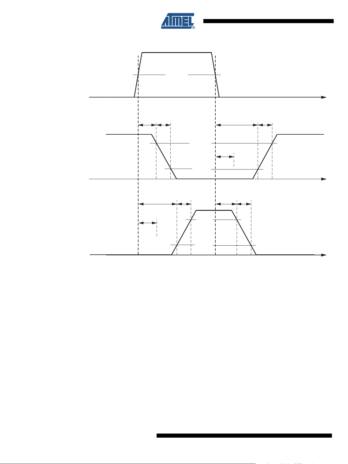
Figure 5-5. Timing of the Drivers
PWM or
DIR
Lx
Hx
t
LxHLtLxf
t
HxLH
t
CC
50%
t
Hxr
80%
20%
80%
t
LxLH
t
CC
t
HxHLtHxf
t
t
Lxr
t
The delays t
5.12 Short Circuit Detection
To detect a short in H-bridge circuitry, internal comparators detect the voltage difference
between source and drain of the external power NMOS. If the transistors are switched ON and
the source-drain voltage difference is higher than the value V
>t
(typically 10 µs) the signal SC (short circuit) will be set and the drivers will be switched off
SC
immediately. The diagnostic pin DG1 will be set to “H”. With the next transition on pin PWM, the
bit will be cleared and the corresponding drivers, depending on the DIR pin, will be switched on
again.
There is a PBAT supervision block implemented to detect the possible voltage drop on PBAT
during a short circuit. If the voltage at PBAT falls under V
>t
the drivers will be switched off immediately and DG1 will be set to “H”. It will be cleared as
SC
above.
HxLH
and t
20%
include the cross conduction time tCC.
LxLH
(4V with tolerances) for a time
SC
(5.6V with tolerances) for a time
SCPB
t
14
ATA6823 [Preliminary]
4856E–AUTO–07/07
Page 15

ATA6823 [Preliminary]
6. Absolute Maximum Ratings
Stresses beyond those listed under “Absolute Maximum Ratings” may cause permanent damage to the device. This is a stress rating
only and functional operation of the device at these or any other conditions beyond those indicated in the operational sections of this
specification is not implied. Exposure to absolute maximum rating conditions for extended periods may affect device reliability.
Pin Description Pin Name Min Max Unit
Ground GND 0 0 V
Power ground PGND –0.3 +0.3 V
Reverse protected battery voltage VBAT –0.3 +40 V
Reverse protected battery voltage PBAT –0.3 +40 V
Digital output /RESET –0.3 V
Digital output DG1, DG2, DG3 –0.3 V
4.9V output, external blocking capacitor VINT –0.3 +5.5 V
Cross conduction time capacitor/resistor
combination
CC –0.3 V
Digital input coming from microcontroller WD –0.3 V
Watchdog timing resistor RWD –0.3 V
Digital input direction control DIR –0.3 V
Digital input PWM control + Test mode PWM –0.3 V
Digital input for enable control EN1 –0.3 V
Digital input for enable control EN2 –0.3 V
5V regulator output VCC –0.3 +5.5 V
Digital input VMODE –0.3 V
12V output, external blocking capacitor VG –0.3 +16 V
Digital output RX –0.3 V
Digital input TX –0.3 V
LIN data pin LIN –27
(1)
Source external high-side NMOS S1, S2 –2 +30 V
Gates external low-side NMOS L1, L2 V
Gates of external high-side NMOS H1, H2 V
– 0.3 V
PGND
– 1 VS + 16 V
S
Charge pump CPLO –0.3 V
Charge pump CPHI –0.3 V
Charge pump output VRES –0.3 +30 V
Switched VBAT VBATSW –0.3 V
Power dissipation P
Storage temperature ϑ
Soldering temperature (10s) ϑ
Notes: 1. For V
VBAT
≤ 13.5V
tot
STORE
SOLDERING
–40 +150 °C
2. May be additionally limited by external thermal resistance
+ 0.3 V
VCC
+ 0.3 V
VCC
+ 0.3 V
VINT
+ 0.3 V
VINT
+ 0.3 V
VCC
+ 0.3 V
VCC
+ 0.3 V
VCC
+ 0.3 V
VCC
+ 0.3 V
VBAT
+ 0.3 V
VINT
+ 0.3 V
VCC
+ 0.3 V
VCC
V
+ 2 V
VBAT
+ 0.3 V
VG
+ 0.3 V
PBAT
+ 0.3 V
VRES
+ 0.3 V
VBAT
(2)
1.4
240 °C
W
4856E–AUTO–07/07
15
Page 16

7. Thermal Resistance
Parameters Symbol Value Unit
Thermal resistance junction to heat slug R
Thermal resistance junction to ambient when heat
slug is soldered to PCB
thjc
R
thja
<5 K/W
25 K/W
8. Operating Range
The operating conditions define the limits for functional operation and parametric characteristics of the device. Functionality outside these
limits is not implied unless otherwise stated explicitly.
Parameters Symbol Min Max Unit
Operating supply voltage
Operating supply voltage
Operating supply voltage
Operating supply voltage
Operating supply voltage
(1)
(2)
(3)
(4)
(5)
Ambient temperature range under bias T
Normal functionality T
Normal functionality, overtemperature warning T
Drivers for H1, H2, L1, L2, and LIN are switched
OFF, VCC regulator is OFF
Note: 1. Full functionality
2. H-bridge drivers may be switched off (undervoltage detection)
3. H-bridge drivers are switched off, 5V/3.3V regulator with reduced parameters, RESET works correctly
4. H-bridge drivers are switched off, 5V regulator not working, RESET not correct
5. H-bridge drivers are switched off
V
V
V
V
V
VBAT1
VBAT2
VBAT3
VBAT4
VBAT5
a
a
a
T
a
718V
6< 7V
3< 6V
0< 3V
> 20 40 V
–40 +125 °C
–40 +125 °C
150 165 °C
165 180 °C
16
ATA6823 [Preliminary]
4856E–AUTO–07/07
Page 17

ATA6823 [Preliminary]
9. Electrical Characteristics
All parameters given are valid for 7V ≤ VBAT ≤ 18V and for –40°C ≤ϑambient ≤ 125°C unless stated otherwise.
No. Parameters Test Conditions Pin Symbol Min Typ Max Unit Type*
1 Power Supply and Supervisor Functions
VBAT
VBAT
(1)
<40V
≤ 9V
25, 30 I
30 V
30 V
30 V
30 V
29 V
29 V
regulation
regulation
VBAT1
VBAT2
INT
BG
THOV
TOVhys
THUV
TUVhys
ON_VBATSW
CC1
CC2
DC line
DC load
OS1
4.84.945.1 V A
1.225 1.235 1.245 V A
19.8 22.3 V A
11.5VA
6.5 7 V A
0.2 0.4 V A
4.85
(3.2)
4.75
(3.2)
<1 50 mV A
<10 50 mV A
100 300 mA C
7mAA
50 µA A
100 Ω A
5.15
(3.4)
5.25
(3.4)
VA
VA
29 ESL 1 20 nH D
29 ESR 0 0.5 Ω D
29 C
VCC
1.5 3.0 µF D
sc
1.1 Current consumption V
Current consumption V
1.2
in Standby mode
BATVVBAT
BAT
= 13.5V
=13.5V 25, 30 I
V
VBAT
1.3 Internal power supply 2 V
1.4 Band gap voltage V
Overvoltage threshold
1.5
V
BAT
Overvoltage threshold
1.6
hysteresis V
Undervoltage threshold
1.7
V
BAT
Undervoltage threshold
1.8
hysteresis V
On resistance of V
1.9
switch
BAT
BAT
BAT
Measured during
qualification only
Measured during
qualification only
V
VBAT
= 13.5V 31 R
2 5V/3.3V Regulator
VCC
VCC
9V < V
= 0 mA to 100 mA
I
load
6V < V
I
= 0 mA to 100 mA
load
= 0 mA to 100 mA 29
load
= 0 mA to 100 mA 29
load
> 6V 29 I
VBAT
(2), (3)
2.1 Regulated output voltage
2.2 Regulated output voltage
2.3 Line regulation I
2.4 Load regulation I
2.5 Output current limitation V
Serial inductance to C
2.6
including PCB
Serial resistance to C
2.7
including PCB
2.8 Blocking cap at VCC
* Type: A = 100% tested, B = 100% correlation tested, C = Characterized on samples, D = Design parameter
Notes: 1. EN, DIR, PWM = high
2. The use of X7R material is recommended
3. For higher values, stability at zero load is not guaranteed
4. Tested during qualification only
5. Value depends on T
; function tested with digital test pattern
OSC
6. Tested during characterization only
7. Supplied by charge pump
8. See section “Cross Conduction Time”
9. Voltage between source-drain of external switching transistors in active case
10. The short-circuit message will never be generated for switch-on time < t
4856E–AUTO–07/07
17
Page 18

9. Electrical Characteristics (Continued)
All parameters given are valid for 7V ≤ VBAT ≤ 18V and for –40°C ≤ϑambient ≤ 125°C unless stated otherwise.
No. Parameters Test Conditions Pin Symbol Min Typ Max Unit Type*
2.9 HIGH threshold VMODE 1 VMODE H 4.0 V A
2.10 LOW threshold VMODE 1 VMODE L 0.7 V A
3 Reset and Watchdog
VCC threshold voltage
3.1
level for /RESET
threshold voltage
V
3.2
3.3
3.4
3.5
3.6
3.7
CC
level for /RESET
Hysteresis of /RESET
level
Length of pulse at
/RESET pin
Length of short pulse at
/RESET pin
Wait for the first WD
trigger
Time for VCC < V
tHRESL
before activating /RESET
Resistor defining internal
3.8
bias currents for
watchdog oscillator
Watchdog oscillator
3.9
period
Watchdog oscillator
3.10
period with internal
resistor
Watchdog input
3.11
low-voltage threshold
Watchdog input
3.12
high-voltage threshold
Hysteresis of watchdog
3.13
input voltage threshold
3.14 Close window
* Type: A = 100% tested, B = 100% correlation tested, C = Characterized on samples, D = Design parameter
Notes: 1. EN, DIR, PWM = high
2. The use of X7R material is recommended
3. For higher values, stability at zero load is not guaranteed
4. Tested during qualification only
5. Value depends on T
6. Tested during characterization only
7. Supplied by charge pump
8. See section “Cross Conduction Time”
9. Voltage between source-drain of external switching transistors in active case
10. The short-circuit message will never be generated for switch-on time < t
VMODE = “H”
(VMODE = “L”)
VMODE = “H”
(VMODE = “L”)
(4)
(5)
(5)
(5)
(4)
29 V
29 V
29 HYS
5t
5t
5t
29 t
3R
R
= 33 kΩ 3T
RWD
6V
6V
6V
(5)
; function tested with digital test pattern
OSC
tHRESH
tHRESL
RESth
res
resshort
d
delayRESL
RWD
OSC
T
OSC_start
ILWD
IHWD
hysWD
t1
4.6
(3.05)
VA
4.1 (2.7) V A
0.2 V A
6800 T
200 T
6800 T
100
100
100
0.5 2 µs C
10 91 kΩ D
11.09 13.55 µs A
16 24 µs A
0.7 ×
V
VCC
0.3 ×
V
VCC
VA
VA
1VA
980 ×
T
OSC
sc
A
A
A
A
18
ATA6823 [Preliminary]
4856E–AUTO–07/07
Page 19

ATA6823 [Preliminary]
9. Electrical Characteristics (Continued)
All parameters given are valid for 7V ≤ VBAT ≤ 18V and for –40°C ≤ϑambient ≤ 125°C unless stated otherwise.
No. Parameters Test Conditions Pin Symbol Min Typ Max Unit Type*
3.15 Open window
Output low-voltage of
3.16
/RESET
Internal pull-up resistor at
3.17
pin /RESET
(5)
At I
= 1 mA 5 V
OLRES
t2
OLRES
5R
PURES
5 10 15 kΩ D
4 Lin Transceiver
4.1 Low-level output current
Normal mode;
V
=0V, VRX=0.4V
LIN
13 IL
RX
4mAD
Normal mode;
4.2 High-level output current
V
LIN=VBAT
13 IH
RX
4mAD
VRX=VCC–0.4V
Driver recessive output
4.3
voltage
Driver dominant voltage
4.4
V
BUSdom_DRV_LoSUP
Driver dominant voltage
4.5
V
BUSdom_DRV_HiSUP
Driver dominant voltage
4.6
V
BUSdom_DRV_LoSUP
Driver dominant voltage
4.7
V
BUSdom_DRV_HiSUP
4.8 Pull up resistor to VS
4.9 Current limitation V
Input leakage current at
the receiver including
4.10
pull-up resistor as
specified
V
TXD
V
VAT
R
load
V
VAT
R
load
V
VAT
R
load
V
VAT
R
load
= 0V; I
= 7.3V
= 500Ω
= 18V
= 500Ω
= 7.3V
= 1000Ω
= 18V
= 1000Ω
= 0 mA 8 V
LIN
The serial diode is
mandatory
= V
BUS
BAT_max
Input leakage current
driver off
= 0V
V
BUS
= 12V
V
BAT
BUSrec
8V
8V
8V
8V
8R
8I
8I
_LoSUP
_HiSUP
_LoSUP_1k
_HiSUP_1k_
LIN
BUS_LIM
BUS_PAS_dom
0.9 ×
VBAT
0.6 V
0.8 V
20 30 60 kΩ D
50 200 mA
–1 mA
Driver off
Leakage current LIN
4.11
recessive
8V < V
8V < V
V
BUS
≥ V
BAT
BUS
< 18V
< 18V
BAT
8I
BUS_PAS_rec
* Type: A = 100% tested, B = 100% correlation tested, C = Characterized on samples, D = Design parameter
Notes: 1. EN, DIR, PWM = high
2. The use of X7R material is recommended
3. For higher values, stability at zero load is not guaranteed
4. Tested during qualification only
5. Value depends on T
; function tested with digital test pattern
OSC
6. Tested during characterization only
7. Supplied by charge pump
8. See section “Cross Conduction Time”
9. Voltage between source-drain of external switching transistors in active case
10. The short-circuit message will never be generated for switch-on time < t
sc
780 ×
T
OSC
0.4 V A
V
1.2 V
2V
20 µA
A
4856E–AUTO–07/07
19
Page 20

9. Electrical Characteristics (Continued)
All parameters given are valid for 7V ≤ VBAT ≤ 18V and for –40°C ≤ϑambient ≤ 125°C unless stated otherwise.
No. Parameters Test Conditions Pin Symbol Min Typ Max Unit Type*
Leakage current at
ground loss
Control unit disconnected
4.12
from ground
Loss of local ground must
GND
V
BAT
0V < V
not affect communication
in the residual network
Node has to sustain the
current that can flow
4.13
under this condition. Bus
must remain operational
V
BAT
V
SUP_Device
0V < V
under this condition
Center of receiver
4.14
threshold
4.15 Receiver dominant state V
4.16 Receiver recessive state V
4.17 Receiver input hysteresis V
Dominant time for
4.18
wake-up via LIN-bus
V
BUS_CNT
(V
EN
EN
HYS
V
LIN
5 Control Inputs EN1, DIR, PWM, WD, TX
Input low-voltage
5.1
threshold
Input high-voltage
5.2
threshold
5.3 Hysteresis
(6)
5.4 Pull-down resistor EN1, DIR, PWN, WD R
5.5 Pull-up resistor TX R
5.6 Rise/fall time t
5.7 Debounce time EN1
(6)
6Charge Pump
6.1 Charge pump voltage Load = 0A 21 VCP
6.2 Charge pump voltage
Load = 3 mA,
C
CP
* Type: A = 100% tested, B = 100% correlation tested, C = Characterized on samples, D = Design parameter
Notes: 1. EN, DIR, PWM = high
2. The use of X7R material is recommended
3. For higher values, stability at zero load is not guaranteed
4. Tested during qualification only
5. Value depends on T
; function tested with digital test pattern
OSC
6. Tested during characterization only
7. Supplied by charge pump
8. See section “Cross Conduction Time”
9. Voltage between source-drain of external switching transistors in active case
10. The short-circuit message will never be generated for switch-on time < t
= VS
Device
=12V
BUS
< 18V
8I
disconnected
= GND
< 18V
BUS
=
th_dom+Vth_rec
)/2
8I
8V
= 5V 8 V
= 5V 8 V
= V
th_rec
– V
th_dom
8V
= 0V 8 T
= 100 nF
21 VCP
BUS_NO_gnd
BUS
BUS_CNT
BUSdom
BUSrec
BUShys
BUS
V
IL
V
IH
–1 1 mA
100 µA
0.475 VS 0.5 VS 0.525 VS V
0.4 VS V
0.6 VS V
0.1 VS 0.175 VS V
30 90 150 µs D
0.7 ×
V
VCC
0.3 ×
V
VCC
VA
VA
HYS 0.7 A
PD
PU
rf
t
db
25 50 100 kΩ D
25 50 100 kΩ D
100 ns D
sc
2 × T
V
+ V
VBAT
VG
100
– 1
3 × T
V
VBAT
+ V
100
VG
µs D
VA
VA
20
ATA6823 [Preliminary]
4856E–AUTO–07/07
Page 21

ATA6823 [Preliminary]
9. Electrical Characteristics (Continued)
All parameters given are valid for 7V ≤ VBAT ≤ 18V and for –40°C ≤ϑambient ≤ 125°C unless stated otherwise.
No. Parameters Test Conditions Pin Symbol Min Typ Max Unit Type*
Period charge pump
6.3
oscillator
CP load current in VG
6.4
without CP load
CP load current in VG
6.5
with CP load
Load = 0A I
Load = 3 mA,
= 100 nF
C
CP
7H-bridge Driver
Low-side driver HIGH
7.1
output voltage
ON-resistance of sink
7.2
stage of pins L1, L2
ON-resistance of source
7.3
stage of pins L1, L2
Output peak current at
7.4
pins L1, L2, switched to
= 3V
V
Lx
LOW
Output peak current at
7.5
pins L1, L2, switched to
V
= 3V
Lx
HIGH
Pull-down resistance at
7.6
pins L1, L2
ON-resistance of sink
7.7
stage of pins H1, H2
ON-resistance of source
7.8
stage of pins H1, H2
Output peak current at
7.9
pins Hx, switched to LOW
Output peak current at
7.10
pins Hx, switched to
HIGH
Static high-side switch
7.11
output low-voltage pins
Hx
V
V
V
V
V
V
V
V
V
I
Hx
Sx
Sx
VBAT
Sx
Hx
VBAT
Sx
Hx
Sx
= 0
= V
VBAT
= 13.5V
= V
VBAT
= V
VBAT
= 13.5V
= V
VBAT
= V
VBAT
= 0V
= 1 mA
+ 3V
+ 3V
* Type: A = 100% tested, B = 100% correlation tested, C = Characterized on samples, D = Design parameter
Notes: 1. EN, DIR, PWM = high
2. The use of X7R material is recommended
3. For higher values, stability at zero load is not guaranteed
4. Tested during qualification only
5. Value depends on T
; function tested with digital test pattern
OSC
6. Tested during characterization only
7. Supplied by charge pump
8. See section “Cross Conduction Time”
9. Voltage between source-drain of external switching transistors in active case
10. The short-circuit message will never be generated for switch-on time < t
T
100
VGCPz
I
VGCP
V
LxH
R
DSON_LxL,
x = 1, 2
R
DSON_LxH,
x = 1, 2
I
LxL,
x = 1, 2
I
LxH,
x = 1, 2
R
PDLx
x = 1, 2
R
DSON_HxL,
x = 1, 2
R
DSON_HxH,
x = 1, 2
I
HxL,
x = 1, 2
I
HxH,
x = 1, 2
V
HxL
x = 1, 2
911µsA
100 µA D
3.3 mA A
V
VG
VD
20 Ω A
20 Ω A
100 mA D
–100 mA D
30 100 kΩ A
20 Ω A
20 Ω A
100 mA D
–100 mA D
,
sc
0.3 V
4856E–AUTO–07/07
21
Page 22

9. Electrical Characteristics (Continued)
All parameters given are valid for 7V ≤ VBAT ≤ 18V and for –40°C ≤ϑambient ≤ 125°C unless stated otherwise.
No. Parameters Test Conditions Pin Symbol Min Typ Max Unit Type*
Static high-side switch
7.12
output high-voltage pins
H1, H2
= –10 µA
I
Lx
(PWM = static)
V
HxHstat1
V
V
VBAT
VG
+
– 1
(7)
Sink resistance between
7.13
Hx and ground in Sleep
R
Hxsleep
310kΩ
mode
Dynamic Parameters
Dynamic high-side switch
7.14
output high-voltage pins
H1, H2
Propagation delay time,
7.15
low-side driver from high
to low
= 5 nF
C
Hx
C
= 100 nF
CB
= 20 kHz
f
PWM
Figure 5-5 on page 14
= 13.5V
V
VBAT
V
HxHdyn1
t
LxHL
V
VBAT
VVG – 1
+
Propagation delay time,
7.16
low-side driver from low to
t
LxLH
high
= 13.5V
V
7.17 Fall time low-side driver
VBAT
CGx=5 nF
7.18 Rise time low-side driver t
Propagation delay time,
7.19
high-side driver from high
to low
Figure 5-5 on page 14
V
= 13.5V
VBAT
t
Lxr
t
HxHL
Lxf
Propagation delay time,
7.20
high-side driver from low
t
HxLH
to high
= 13.5V,
V
7.21 Fall time high-side driver
C
VBAT
Gx
= 5 nF
7.22 Rise time high-side driver t
7.23 Cross conduction time
(8)
7.24 External resistor R
7.25 External capacitor C
of tCC switching
R
7.26
ON
transistor
R
t
Hxf
Hxr
t
CC
CC
CC
ONCC
5kΩ
* Type: A = 100% tested, B = 100% correlation tested, C = Characterized on samples, D = Design parameter
Notes: 1. EN, DIR, PWM = high
2. The use of X7R material is recommended
3. For higher values, stability at zero load is not guaranteed
4. Tested during qualification only
5. Value depends on T
; function tested with digital test pattern
OSC
6. Tested during characterization only
7. Supplied by charge pump
8. See section “Cross Conduction Time”
9. Voltage between source-drain of external switching transistors in active case
10. The short-circuit message will never be generated for switch-on time < t
sc
V
+
V
VBAT
V
VBAT
V
VG
+
VG
V
V
0.5 µs
0.5 + t
CC
µs
0.5 µs
0.5 µs
0.5 µs
0.5 + t
CC
µs
0.5 µs
0.5 µs
10 µs
5nF
100 Ω
22
ATA6823 [Preliminary]
4856E–AUTO–07/07
Page 23

ATA6823 [Preliminary]
9. Electrical Characteristics (Continued)
All parameters given are valid for 7V ≤ VBAT ≤ 18V and for –40°C ≤ϑambient ≤ 125°C unless stated otherwise.
No. Parameters Test Conditions Pin Symbol Min Typ Max Unit Type*
Switching level of t
7.27
comparator
Short circuit detection
7.28
voltage
Short circuit detection
7.29
time
8 Input EN2
Input low-voltage
8.1
threshold
Input high-voltage
8.2
threshold
8.3 Hysteresis
8.4 Pull-down resistor R
8.5 Rise/fall time t
8.6 Debounce time
9 Diagnostic Outputs DG1, DG2, DG3
9.1 Low level output current V
9.2 High level output current V
* Type: A = 100% tested, B = 100% correlation tested, C = Characterized on samples, D = Design parameter
Notes: 1. EN, DIR, PWM = high
2. The use of X7R material is recommended
3. For higher values, stability at zero load is not guaranteed
4. Tested during qualification only
5. Value depends on T
6. Tested during characterization only
7. Supplied by charge pump
8. See section “Cross Conduction Time”
9. Voltage between source-drain of external switching transistors in active case
10. The short-circuit message will never be generated for switch-on time < t
CC
(9)
(10)
(6)
(6)
(6)
= 0.4V
DG
= VCC – 0.4V
DG
; function tested with digital test pattern
OSC
(6)
V
swtcc
V
SC
t
SC
V
V
0.653 ×
V
3.544.5V
IL
IH
2.3 3.6 V
2.8 4.0 V
VCC
0.667 ×
V
VCC
0.68 ×
V
VCC
51015ms
HYS 0.47 V
PD
rf
t
db
50 100 200 kΩ
100 ns
2 × T
100
3 × T
100
IL 4 mA
IH 4 mA
sc
V
µs
4856E–AUTO–07/07
23
Page 24

10. Schaffner and Electromagnetic Compatibility
10.1 Transients on Power-supply Rail (Battery)
The application (including IC and external protection circuitry, see Figure 1-1 on page 2) has to
withstand the test pulses in Table 10-1.
Table 10-1. Test Pulses
Test
Pulse No.
1 –100V 10 min R
2 150V 10 min R
3a –200V 10 min R
3b 200V 10 min R
4 4V/5.5V 15 ms/2s R
540V
Test
Level
Duration or Number
of Pulses Specs
5 pulses, 1 minute
recurrence period
Acceptance
= 10Ω A
i
= 10Ω A
i
= 50Ω A
i
= 50Ω A
i
= 0.01Ω A
i
R
= 0.5Ω, td = 400 ms, tr = 5 ms B
i
level
Figure 10-1. Pulse 1 (R
V
12V
-100V
Figure 10-2. Pulse 2 (R
150V
= 10Ω)
i
90%
= 10Ω)
i
V
200 ms
< 100 µs
t10%
1 µs
1 ms
5s
200 ms
50 µs
2 µs
90%
24
12V
ATA6823 [Preliminary]
10%
50 µs
t
4856E–AUTO–07/07
Page 25

Figure 10-3. Pulse 3a (Ri = 50Ω)
V
12V
-200V
10 ms
100 µs
90 ms
ATA6823 [Preliminary]
100 ns
5 ns
t
10%
90%
Figure 10-4. Pulse 3b (R
V
200V
12V
100 µs
Figure 10-5. Pulse 4 (R
12V
= 50Ω)
i
= 0.01Ω)
i
90%
10%
90 ms10 ms
t
5 ns
100 ns
4856E–AUTO–07/07
5.5V
4.0V
0V
t
15 ms 2000 ms50 ms 100 ms< 5 ms
25
Page 26

10.2 Transients on Pin LIN
Transients to these pins are coupled capacitively to the IC and are valid for the application with
external circuitry concerning figure 6.
Values: Pulse 3a, Pulse 3b (see Figure 10-3 and Figure 10-4 on page 25) coupled via 1 nF to
LIN, R
Acceptance level A
=50Ω
i
10.3 Conducted Emissions, Radiated Emissions and Susceptibility
The application using the IC described in this specification has to fulfill the demands of the following specifications:
• GM GMW3100 (2001-08)
• TL82166 (1998-02)
• TL82366 (2002-03)
• TL965 (1999-10)
It is the responsibility of both the deliverer and the user of the described IC to meet the mentioned specifications.
11. ESD and Latch-up Requirements
The device withstands pulses when tested according to ESD STM 5.1-1998:
• Constant voltage 2 kV
• R = 1.5 kΩ
• C = 100 pF
1 pulse per polarity and per pin
3 samples, 0 failures
Electrical post stress testing at room temperature
Static latch-up tested according to AEC-Q100-004 and JESD78.
• 3 to 6 samples, 0 failures
• Electrical post stress testing at room temperature
In test, the voltage at the pins VBAT, LIN, CP, VBATSW, Hx, and Sx must not exceed 45V when
not able to drive the specified current.
26
ATA6823 [Preliminary]
4856E–AUTO–07/07
Page 27

ATA6823 [Preliminary]
12. Ordering Information
Extended Type Number Package Remarks
ATA6823-PHQY QFN32 Pb-free
13. Package Information
Package: QFN 32 - 7 x 7
Exposed pad 4.7 x 4.7
Dimensions in mm
Not indicated tolerances ± 0.05
32
1
8
Drawing-No.: 6.543-5097.01-4
Issue: 1; 24.02.03
14. Revision History
0.9±0.1
+0
0.05-0.05
0.3
0.6
24
17
7
4.7
3225
1
technical drawings
according to DIN
specifications
8
916
0.65 nom.
4.55
4856E–AUTO–07/07
Please note that the following page numbers referred to in this section refer to the specific revision
mentioned, not to this document.
Revision No. History
4856E-AUTO-07/07 • Put datasheet in a new template
27
Page 28

Headquarters International
Atmel Corporation
2325 Orchard Parkway
San Jose, CA 95131
USA
Tel: 1(408) 441-0311
Fax: 1(408) 487-2600
Atmel Asia
Room 1219
Chinachem Golden Plaza
77 Mody Road Tsimshatsui
East Kowloon
Hong Kong
Tel: (852) 2721-9778
Fax: (852) 2722-1369
Product Contact
Web Site
www.atmel.com
Literature Requests
www.atmel.com/literature
Atmel Europe
Le Krebs
8, Rue Jean-Pierre Timbaud
BP 309
78054
Saint-Quentin-en-Yvelines Cedex
France
Tel: (33) 1-30-60-70-00
Fax: (33) 1-30-60-71-11
Technical Support
auto_control@atmel.com
Atmel Japan
9F, Tonetsu Shinkawa Bldg.
1-24-8 Shinkawa
Chuo-ku, Tokyo 104-0033
Japan
Tel: (81) 3-3523-3551
Fax: (81) 3-3523-7581
Sales Contact
www.atmel.com/contacts
Disclaimer: The information in this document is provided in connection with Atmel products. No license, express or implied, by estoppel or otherwise, to any
intellectual property right is granted by this document or in connection with the sale of Atmel products. EXCEPT AS SET FORTH IN ATMEL’S TERMS AND CONDI-
TIONS OF SALE LOCATED ON ATMEL’S WEB SITE, ATMEL ASSUMES NO LIABILITY WHATSOEVER AND DISCLAIMS ANY EXPRESS, IMPLIED OR STATUTORY
WARRANTY RELATING TO ITS PRODUCTS INCLUDING, BUT NOT LIMITED TO, THE IMPLIED WARRANTY OF MERCHANTABILITY, FITNESS FOR A PARTICULAR
PURPOSE, OR NON-INFRINGEMENT. IN NO EVENT SHALL ATMEL BE LIABLE FOR ANY DIRECT, INDIRECT, CONSEQUENTIAL, PUNITIVE, SPECIAL OR INCIDENTAL DAMAGES (INCLUDING, WITHOUT LIMITATION, DAMAGES FOR LOSS OF PROFITS, BUSINESS INTERRUPTION, OR LOSS OF INFORMATION) ARISING OUT OF
THE USE OR INABILITY TO USE THIS DOCUMENT, EVEN IF ATMEL HAS BEEN ADVISED OF THE POSSIBILITY OF SUCH DAMAGES. Atmel makes no
representations or warranties with respect to the accuracy or completeness of the contents of this document and reserves the right to make changes to specifications
and product descriptions at any time without notice. Atmel does not make any commitment to update the information contained herein. Unless specifically provided
otherwise, Atmel products are not suitable for, and shall not be used in, automotive applications. Atmel’s products are not intended, authorized, or warranted for use
as components in applications intended to support or sustain life.
© 2007 Atmel Corporation. All rights reserved. Atmel®, logo and combinations thereof, and others are registered trademarks or trademarks of
Atmel Corporation or its subsidiaries. Other terms and product names may be trademarks of others.
4856E–AUTO–07/07
 Loading...