

Page 1

Features
• Operating Range from 5V to 27V
• Baud Rate up to 20Kbaud
• LIN Physical Layer According to LIN Specification 2.0, 2.1 and SAEJ2602-2
• Fully Compatible with 3.3V and 5V Devices
• TXD Dominant Timeout Timer
• Normal and Sleep Mode
• Wake-up Capability via LIN Bus (90µs Dominant)
• Very Low Standby Current During Sleep Mode (10µA)
• Bus Pin is Overtemperature and Short-circuit Protected Versus GND and Battery
• LIN Input Current < 2µA if VBAT Is Disconnected
• Overtemperature Protection
• High EMC Level
• Interference and Damage Protection According to ISO/CD 7637
• Fulfills the OEM Hardware Requirements for LIN in Automotive Applications Rev. 1.1
• Transceiver 2: Additional INH High Side Switch Output and High Voltage WAKE Input
Dual LIN
Transceiver
Atmel ATA6670
1. Description
The Atmel® ATA6670 is a fully integrated Dual-LIN transceiver complying with the LIN
specification 2.0, 2.1, and SAEJ2602-2. There are two completely independent and
separated LIN transceivers integrated in one package (only the GND pins GND1 and
GND2 are internally connected). Each of them interfaces with the LIN protocol handler
and the physical layer.
The two LIN transceivers are nearly identical, the only difference is an additional wake
input and an INH output at transceiver 2.
The device is designed to handle the low-speed data communication in vehicles, for
example, in convenience electronics. Improved slope control at the LIN bus ensures
secure data communication of up to 20Kbaud with an RC oscillator for protocol handling. Sleep mode guarantees minimal current consumption for each transceiver even
in the case of a floating bus line or a short-circuit on the LIN bus to GND. The Atmel
ATA6670 features advanced EMI and ESD performance.
Preliminary
9204C–AUTO–09/11
Page 2
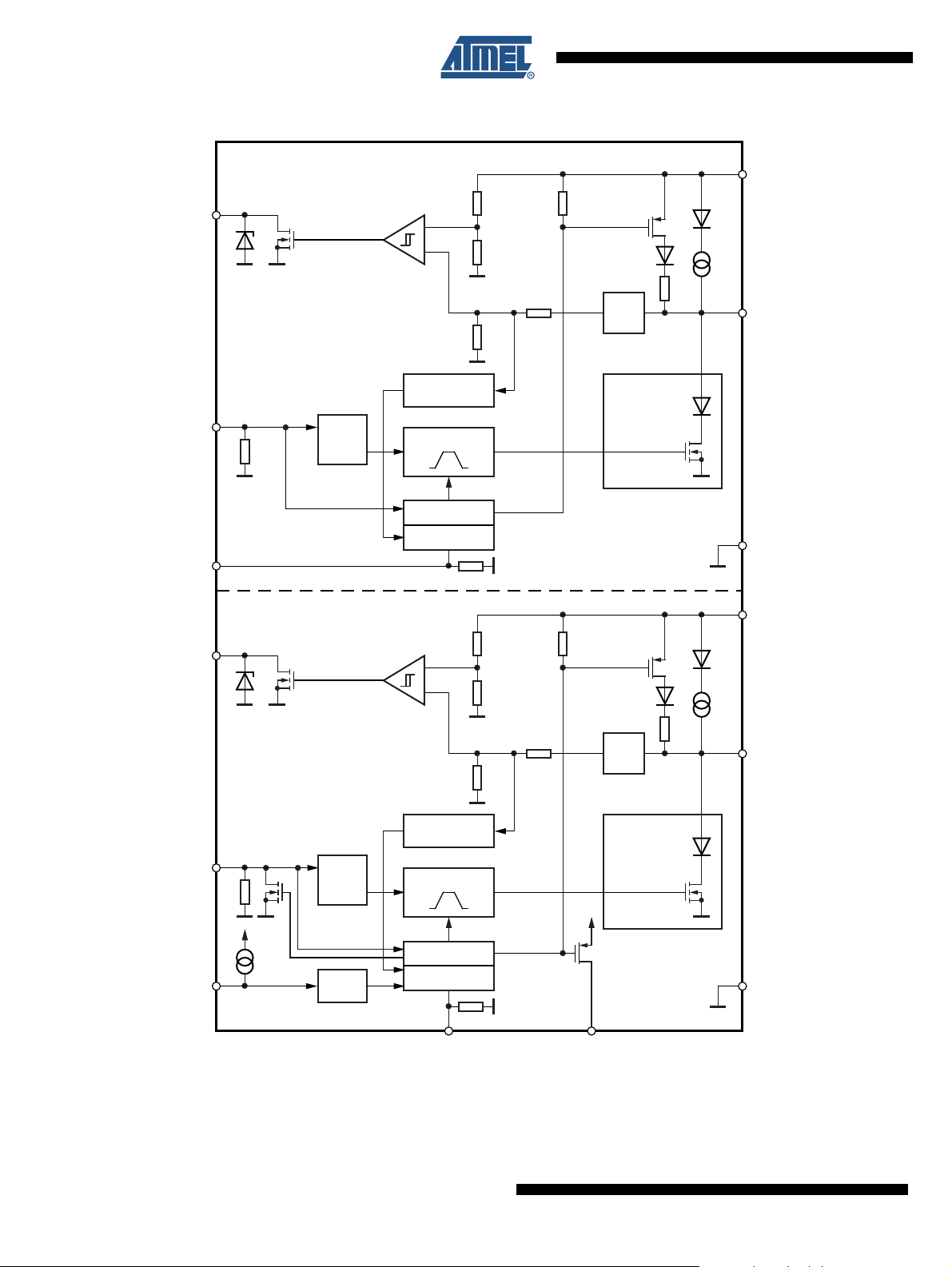
Figure 1-1. Block Diagram
Receiver
+
-
Wake up bus
timer
Slew rate control
Control unit
Filter
Short circuit
and over-
temperature
protection
TXD
Time-Out
Timer
Sleep mode
Receiver
4
RXD2
1
RXD1
TXD2
GND2WAKE2
EN2
7
Transceiver 2
Transceiver 1
V
S
V
S
+
-
Wake up bus
timer
Slew rate control
Control unit
Filter
Short circuit
and over-
temperature
protection
TXD
Time-Out
Timer
Wake-up
Timer
Sleep mode
TXD1
3
EN1
2
6 8
5
GND1
12
LIN2
9
LIN1
13
VS2
10
VS1
14
INH2
11
2
Atmel ATA6670 [Preliminary]
9204C–AUTO–09/11
Page 3
2. Pin Configuration
Figure 2-1. Pinning DFN14
Atmel ATA6670 [Preliminary]
RXD1
EN1
TXD1
RXD2
EN2
WAKE2
TXD2
Atmel
ATA6670
VS1
LIN1
GND1
INH2
VS2
LIN2
GND2
Table 2-1. Pin Description
Pin Symbol Function
1 RXD1 Receives data output 1 (open drain)
2 EN1 Enables normal mode 1. When the input is open or low, transceiver 1 is in sleep mode.
3 TXD1 Transmits data input 1, active low output (strong pull-down) after a local wake-up request
4 RXD2 Receives data output 2 (open drain)
5 EN2 Enables normal mode 2. When the input is open or low, transceiver 2 is in sleep mode.
6 WAKE2 High voltage input for local wake-up request. If not needed, connect directly to VS2
7 TXD2 Transmits data input 2, active low output (strong pull-down) after a local wake-up request
8 GND2 Ground 2
9 LIN2 LIN bus line 2 input/output
10 VS2 Battery supply 2
11 INH2 VS2- related high-side switch output for controlling an external load, such as a voltage divider
12 GND1 Ground 1
13 LIN1 LIN bus line 1 input/output
14 VS1 Battery supply 1
9204C–AUTO–09/11
3
Page 4

3. Functional Description
The functions described in the following text apply to each LIN transceiver. Therefore, if pin
LIN is stated, this applies to each of the two receivers (LIN1 and LIN2), which work completely
independently. The only internal connection is between GND1 and GND2. The functions only
available at transceiver 2 are marked accordingly.
3.1 Physical Layer Compatibility
Since the LIN physical layer is independent of higher LIN layers (e.g., the LIN protocol layer),
all nodes with a LIN physical layer according to revision 2.x can be mixed with LIN physical
layer nodes, which are based on older versions (i.e., LIN 1.0, LIN 1.1, LIN 1.2, LIN 1.3) without
any restrictions.
3.2 Supply Pin (VS)
Undervoltage detection is implemented to disable transmission if VS falls to a value below 5V
in order to avoid false bus messages. After switching on VS, the corresponding transceiver
switches to fail-safe mode. The supply current for each transceiver in sleep mode is typically
10µA.
3.3 Ground Pin (GND)
The Atmel ATA6670 does not affect the LIN bus in case of GND disconnection. It is able to
handle a ground shift up to 11.5% of V
.
S
3.4 Bus Pin (LIN)
A low-side driver with internal current limitation and thermal shutdown and an internal pull-up
resistor are implemented as specified for LIN 2.x. The voltage range is from –27V to +40V.
This pin exhibits no reverse current from the LIN bus to V
disconnection. The LIN receiver thresholds are compatible with the LIN protocol specification.
The fall time (from recessive to dominant) and the rise time (from dominant to recessive) are
slope-controlled. The output has a self-adapting short-circuit limitation; in other words, during
current limitation, the current decreases in proportion to an increase in chip temperature.
Note: The internal pull-up resistor is only active in normal and fail-safe mode.
3.5 Input/ Pin (TXD)
In normal mode the TXD pin is the microcontroller interface to control the state of the LIN output. TXD must be at the low level in order to have a low LIN bus. If TXD is high, the LIN output
transistor is turned off and the bus is in recessive state. The TXD pin is compatible with both a
3.3V and 5V supply.
3.6 TXD Dominant Time-out Function
The TXD input has an internal pull-down resistor. An internal timer prevents the bus line from
being driven permanently in dominant state. If TXD is forced to low longer than t
the LIN pin is switched off (recessive mode). To reset this mode, switch TXD to high (> 10µs)
before switching LIN to dominant again.
, even in case of a GND shift or V
S
> 40ms,
DOM
Batt
4
Atmel ATA6670 [Preliminary]
9204C–AUTO–09/11
Page 5

Atmel ATA6670 [Preliminary]
3.7 Output Pin (RXD)
This pin reports the state of the LIN bus to the microcontroller. LIN high (recessive) is reported
by a high level at RXD, LIN low (dominant) is reported by a low voltage at RXD. The output is
an open drain, therefore it is compatible with a 3.3V or 5V power supply. The AC characteristics are defined with a pull-up resistor of 5kΩ to 5V and a load capacitor of 20pF. The output
is short current protected. In unpowered mode (V
tion a Zener diode is integrated with V
=6.1V.
Z
3.8 Enable Input Pin (EN)
This pin controls the operation mode of the LIN transceiver. If EN = 1, the LIN transceiver is in
normal mode, with the transmission path from TXD to LIN and from LIN to RXD both active. At
a falling edge on EN, while TXD is already set to high, the device is switched to sleep mode
and no transmission is possible. In sleep mode, the LIN bus pin is connected to V
weak pull-up current source. The device can transmit only after being woken up. During sleep
mode the device is still supplied from the battery voltage. The supply current is typically 10µA.
The pin EN provides a pull-down resistor in order to force the transceiver into sleep mode in
case the pin is disconnected.
3.9 WAKE-up Input Pin (WAKE2, Only Available at Transceiver 2)
This pin is a high-voltage input used to wake up the transceiver 2 from sleep mode. It is usually connected to an external transistor or a switch to generate a local wake-up. A pull-up
current source with typically –10µA is implemented as well as a debounce timer with a typical
debounce time of 70µs.
= 0V) RXD is switched off. For ESD protec-
S
with a
S
Even if the WAKE2 pin is pulled to GND, it is possible to switch the transceiver 2 into sleep
mode.
If a local wake-up is not needed in the application, pin WAKE2 can be connected directly to pin
VS2.
3.10 INH Output Pin (INH2, only available at Transceiver 2)
This pin is used to control an external load or to switch the LIN master pull-up resistor on/off at
pin LIN2. The inhibit pin provides an internal switch towards VS2 which is protected by temperature monitoring. If transceiver 2 is in normal or fail-safe mode, the inhibit high-side switch
is turned on. When the transceiver 2 is in sleep mode, the inhibit switch is turned off, thus disabling the connected external devices.
A wake-up event on LIN2 or at pin WAKE2 puts the transceiver 2 into fail-safe mode and as a
result the INH2 switches to the VS2 level. After a system power-up (VS2 rises from zero), the
pin INH2 switches automatically to the VS2 level.
9204C–AUTO–09/11
5
Page 6
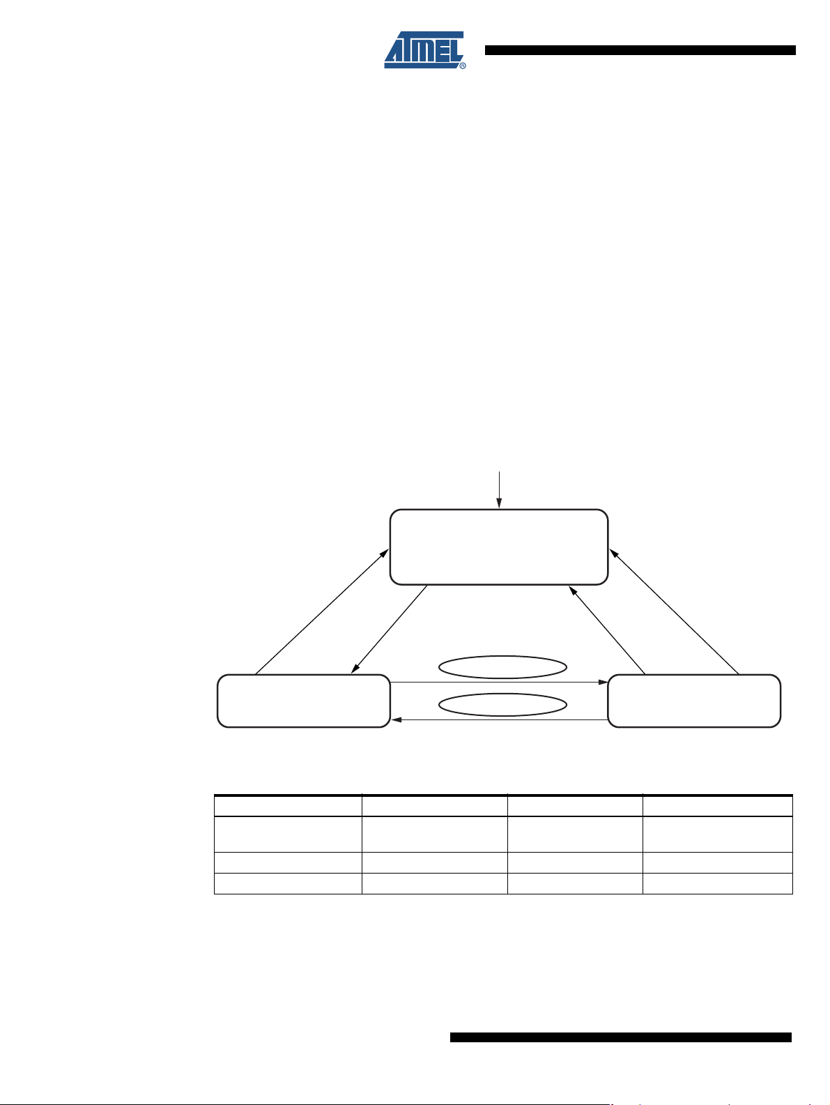
3.11 Operation Modes
a: Power-up (VS > 3V)
b: V
S
< 5V
c: Bus wake-up event
(only Transceiver 2)
d: Wake-up from wake switch
EN = 1
and not b
c or d
bb
a
EN = 0
EN = 1
Fail-Safe Mode
Power-up
Communication: OFF
RXD: see table of Modes
Tr ansceiver 2: INH2 switch ON if VS2 > 5V
Sleep Mode
Communication: OFF
Tr ansceiver 2: INH2 switch OFF
Normal Mode
Communication: ON
Tr ansceiver 2: INH2 switch ON
Local wake-up event
Go to sleep command
1. Normal mode
This is the normal transmitting and receiving mode. All features are available.
2. Sleep mode
In this mode the transmission path is disabled and the device is in low power mode.
Supply current from V
is typically 10µA. A wake-up signal (either from the LIN bus
Batt
or the WAKE2 input) is detected and switches the corresponding transceiver to
fail-safe mode. If EN then switches to high, normal mode is activated. Input debounce
timers at pin WAKE2 (t
WAKE
), LIN (t
) and EN (t
BUS
sleep,tnom
) prevent undesirable
wake-up events due to automotive transients or EMI. The internal termination between pin LIN and pin VS is disabled. Only a weak pull-up current (typical 10µA)
between pin LIN and pin VS is present. Sleep mode can be activated independently
of the current level on pin LIN.
3. Fail-safe mode
At system power-up or after a wake-up event, the transceiver automatically switches
to fail-safe mode. When VS2 exceeds 5V, the transceiver 2 switches the INH2 pin to
the VS2 level. LIN communication is switched off. The microcontroller of the application then confirms normal mode by setting the EN pin to high.
Figure 3-1. Operating Modes
6
Atmel ATA6670 [Preliminary]
Table 3-1. Table of Modes
Operating Mode Transceiver RXD LIN
Fail-safe Off
Normal On LIN-depending TXD-depending
Sleep Off High-ohmic Recessive
High, except after
wake-up
Recessive
9204C–AUTO–09/11
Page 7

3.12 Remote Wake-up via Dominant Bus State
LIN Bus
RXD
EN
High or floating
Normal
Mode
EN High
Node in sleep state
Low
Bus wake-up filtering time
(t
BUS
)
A voltage lower than the LIN pre-wake detection VLINL at pin LIN activates the internal LIN
receiver and starts the wake-up detection timer.
Atmel ATA6670 [Preliminary]
A falling edge at pin LIN, followed by a dominant bus level V
period of time (> t
) and a rising edge at pin LIN results in a remote wake-up request. The
BUS
maintained for a certain
BUSdom
transceiver switches to fail-safe mode, at transceiver 2 the INH2 output is activated (switches
to VS2) and the internal termination resistor is switched on. The remote wake-up request is
indicated by a low level at pin RXD to interrupt the microcontroller (see Figure 3-2).
Figure 3-2. LIN Wake-up Waveform Diagram
In sleep mode the device has a very low current consumption even during short-circuits or
floating conditions on the bus. A floating bus can arise if the master pull-up resistor is missing,
e.g., it is switched off when the LIN master is in sleep mode or even if the power supply of the
master node is switched off.
9204C–AUTO–09/11
In order to minimize the current consumption I
LIN pre-wake threshold, the receiver is activated only for a specific time t
while the voltage at the bus is lower than pre-wake detection low (V
LIN-dominant level, the receiver is switched off again and the circuit reverts to sleep mode.
The current consumption is then the result of I
ched on the bus, no wake-up will occur. Even if the voltage rises above the pre-wake detection
high (V
This means the LIN bus must be above the pre-wake detection threshold V
microseconds before a new LIN wake-up is possible.
during voltage levels at the LIN pin below the
VS
plus I
VSsleep
), the IC will stay in sleep mode (see Figure 3-3 on page 8).
LINH
LINwake
. If t
mon
) and higher than the
LINL
elapses
mon
. If a dominant state is rea-
for a few
LINH
7
Page 8

Figure 3-3. Floating LIN Bus During Sleep Mode
V
LIN BUS
I
VS
LINL
V
BUSdom
I
VSsleep
t
mon
I
VSfail
I
VSsleep
+ I
LINwake
LIN Pre-wake
LIN dominant state
I
VSsleep
Mode of
operation
Int. Pull-up
Resistor
If the Atmel
(V
LIN<VBUSdom
Sleep Mode Sleep Mode
RLIN
®
ATA6670 is in sleep mode and the voltage level at the LIN is in dominant state
) for a period of time exceeding t
Wake-up Detection Phase
off (disabled)
(during a short circuit at LIN, for example),
mon
the IC switches back to sleep mode. The VS current consumption then consists of I
I
LINWAKE
. After a positive edge at pin LIN the IC switches directly to fail-safe mode (see Figure
3-4).
Figure 3-4. Short-circuit to GND on the LIN Bus During Sleep Mode
LIN Pre-wake
V
LIN BUS
LINL
V
BUSdom
t
mon
t
LIN dominant state
mon
VSsleep
plus
I
I
VS
Mode of
operation
Int. Pull-up
Resistor
RLIN
8
Atmel ATA6670 [Preliminary]
I
VSsleep
Wake-up Detection PhaseSleep Mode Fail-Safe Mode
off (disabled) on (enabled)
VSfail
I
VSsleep
+ I
LINwake
Sleep Mode
9204C–AUTO–09/11
Page 9

Atmel ATA6670 [Preliminary]
3.13 Local WAKE-up via Pin WAKE2 (Only Available at Transceiver 2)
A falling edge at pin WAKE2 followed by a low level maintained for a certain period of time
(> t
that no transients create a wake-up. The transceiver 2 then switches to fail-safe mode. Pin
INH2 is activated (switches to VS2) and the internal slave termination resistor is switched on.
The local wake-up request is indicated by a low level at pin RXD for interrupting the microcontroller and by a strong pull-down at pin TXD. (see Figure 3-5).
The voltage threshold for a wake-up signal is 3V below the VS2 voltage with an output current
of typically –3µA. Even in the case of a continuos low at pin WAKE2 it is possible to switch the
transceiver 2 into sleep mode via a low level at pin EN2. The transceiver 2 will remain in sleep
mode for an unlimited time. To generate a new wake-up at pin WAKE2, a high signal for > 6µs
is required. A negative edge then restarts the wake-up filtering time.
Figure 3-5. LIN Transceiver 2: Wake-up from Wake-up Switch (WAKE2)
) results in a local wake-up request. According to ISO 7637, the wake-up time ensures
WAKE
Wake2 Pin
INH2
RXD2
TXD2
EN2
State change
Low or floating
High or floating
TXD weak pull-down resistor
Wake filtering time
t
WAKE
Node in sleep state
High
Low
TXD strong pull-down
Microcontroller start-up
delay time
Low
Weak
pull-down
Node in
operation
EN High
9204C–AUTO–09/11
9
Page 10

3.14 Wake- up Source Recognition (Only available at Transceiver 2)
Transceiver 2 can distinguish between a local wake-up request at pin WAKE2 and a remote
wake-up request via LIN 2. The wake-up source can be read at pin TXD in fail-safe mode. If an
external pull up resistor (typ. 5kΩ) has been added on pin TXD2 to the power supply of the
microcontroller, a high level indicates a remote wake-up request (weak pull down at pin
TXD2), a low level indicates a local wake-up request (strong pull down at pin TXD2).
The wake-up request flag (indicated at pin RXD2) as well as the wake-up source flag (indicated at pin TXD2) are immediately reset if the microcontroller sets pin EN2 to high (see Figure
3-5 on page 9).
3.15 Fail-safe Features
• During a short-circuit at LIN to V
Due to the power dissipation, the chip temperature exceeds T
switched off. The chip cools down and after a hysteresis of T
again.
• During a short-circuit from LIN to GND the transceiver can be switched into sleep mode
and even in this case the current consumption is lower than 45µA. If the short-circuit
disappears, the transceiver starts with a remote wake-up.
• If a transceiver is in sleep mode and a floating condition occurs on the bus, the transceiver
automatically switches back to sleep mode, thus decreasing current consumption to less
than 45µA in this case.
• The reverse current is < 2µA at pin LIN during loss of V
systems where some slave nodes are supplied from battery or ignition.
• Pin EN provides a pull-down resistor to force the transceiver into sleep mode if EN is
disconnected.
• Pin RXD is set to floating if V
BAT
• Pin TXD provides a pull-down resistor to provide a static low if TXD is disconnected.
• After switching the LIN transceiver into Normal Mode the TXD pin must be pulled to high
longer than 10µs in order to activate the LIN driver. This feature prevents the bus from
being driven into dominant state when the LIN transceiver is switched into Normal Mode
and TXD is low.
• The INH2 output transistor at transceiver 2 is protected by temperature monitoring
, the output limits the output current to IBUS_LIM.
Battery
BAT
is disconnected.
, and the LIN output is
off
it switches the output on
hys
; this is optimal behavior for bus
10
Atmel ATA6670 [Preliminary]
9204C–AUTO–09/11
Page 11

Atmel ATA6670 [Preliminary]
4. Absolute Maximum Ratings
Stresses beyond those listed under “Absolute Maximum Ratings” may cause permanent damage to the device. This is a stress rating
only and functional operation of the device at these or any other conditions beyond those indicated in the operational sections of this
specification is not implied. Exposure to absolute maximum rating conditions for extended periods may affect device reliability.
Parameters Symbol Min. Typ. Max. Unit
, V
V
S1
S2
- Continuous supply voltage
WAKE2
- DC and transient voltage (with 2.7kΩ serial resistor)
- Transient voltage according to ISO7637 (coupling 1nF)
Logic pins (RXD1, RXD2, TXD1, TXD2, EN1, EN2) –0.3 +5.5 V
LIN1, LIN2
- DC voltage
- Transient voltage according to ISO7637 (coupling 1nF)
INH2
- DC voltage
ESD according to IBEE LIN EMC
Test specification 1.0 following IEC 61000-4-2
- Pin VS1, VS2, LIN1, LIN2 to GND
- Pin WAKE2 (2.7kΩ serial resistor)
ESD HBM following STM5.1
with 1.5kΩ / 100pF
- Pin VS1, VS2, LIN1, LIN2, WAKE2, INH2 to GND ±6 KV
HBM ESD
ANSI/ESD-STM5.1
JESD22-A114
AEC-Q100 (002)
CDM ESD STM 5.3.1 ±750 V
Machine model ESD AEC-Q100-Rev.F (003) ±200 V
Junction temperature T
Storage temperature T
j
stg
–0.3 +40 V
–27
–150
–27
–150
–0.3 V
+40
+100
+40
+100
+ 0.3 V
S2
±8
±6
±3 KV
–40 +150 °C
–55 +150 °C
V
V
V
V
KV
KV
5. Thermal Characteristics
Parameters Symbol Min. Typ. Max. Unit
Thermal resistance junction to heat slug R
Thermal resistance junction to ambient, where heat slug is
soldered to PCB according to Jedec
Thermal shutdown T
Thermal shutdown hysteresis T
9204C–AUTO–09/11
thJC
R
thJA
off
hys
150 165 180 °C
5 1020°C
8K/W
45 K/W
11
Page 12

6. Electrical Characteristics
5V < VS < 27V, Tj = –40°C to +150°C; the values below are valid for each of the two nearly identical integrated LIN transceivers unless
otherwise specified.
No. Parameters Test Conditions Pin Symbol Min. Typ. Max. Unit Type*
Pin
1V
S
1.1 DC voltage range nominal VS V
S
Sleep mode
V
> VS – 0.5V
LIN
VS I
VSsleep
VS < 14V
1.2 Supply current in sleep mode
Sleep mode,
bus shorted to GND
= 0V
V
LIN
VS I
VSsleep_sc
VS < 14V
1.3
Supply current in normal mode
1.4
Bus recessive
V
< 14V
S
Bus dominant
VS < 14V
VS I
VS I
VSrec
VSdom
Total bus load > 500Ω
1.5 Supply current in fail-safe mode
1.6 VS undervoltage threshold on VS V
1.7 V
1.8
undervoltage threshold off VS V
S
V
undervoltage threshold
S
hysteresis
Bus recessive
< 14V
V
S
VS I
VS V
VSfail
Sth
Sth
Sth_hys
2 RXD Output Pin (Open Drain)
2.1 Low-level output sink current
2.2 RXD saturation voltage 5-kΩ pull-up resistor to 5V RXD Vsat
2.3 High-level leakage current
2.4 ESD Zener diode I
Normal mode
V
LIN
= 0V, V
RXD
= 0.4V
Normal mode
V
= V
, V
LIN
BAT
= 100µA RXD VZ
RXD
RXD
= 5V
RXD I
RXD I
RXDL
RXD
RXDH
RXD
3 TXD Input/Output Pin
3.1 Low-level voltage input TXD V
3.2 High-level voltage input TXD V
3.3 Pull-down resistor V
3.4 Low-level leakage current V
= 5V TXD R
TXD
= 0V TXD I
TXD
TXDL
TXDH
TXD
TXD_leak
Transceiver 2: fail-safe mode,
Low-level output sink current
3.5
(only available at transceiver 2)
local wake-up
= 0.4V
V
TXD2
V
= V
LIN2
BAT
TXD2 I
TXD2
4EN Input Pin
4.1 Low-level voltage input EN V
4.2 High-level voltage input EN V
4.3 Pull-down resistor V
4.4 Low-level input current V
= 5V EN R
EN
= 0V EN I
EN
ENL
ENH
EN
EN
*) Type means: A = 100% tested, B = 100% correlation tested, C = Characterized on samples, D = Design parameter
513.527VA
10 20 µA A
23 45 µA A
0.9 1.3 mA A
1.2 2 mA A
0.5 1.1 mA A
44.95VA
4.05 5 V A
50 500 mV A
1.3 2.5 8 mA A
0.4 V A
–3 +3 µA A
5.8 8.6 V A
–0.3 +0.8 V A
27VA
125 250 600 kΩ A
–3 +3 µA A
1.3 2.5 8 mA A
–0.3 +0.8 V A
27VA
125 250 600 kΩ A
–3 +3 µA A
12
Atmel ATA6670 [Preliminary]
9204C–AUTO–09/11
Page 13

Atmel ATA6670 [Preliminary]
6. Electrical Characteristics (Continued)
5V < VS < 27V, Tj = –40°C to +150°C; the values below are valid for each of the two nearly identical integrated LIN transceivers unless
otherwise specified.
No. Parameters Test Conditions Pin Symbol Min. Typ. Max. Unit Type*
5 INH 2 Output Pin (Only Available at Transceiver 2)
5.1 High-level voltage
Switch-on resistance between
5.2
VS2 and INH2
5.3 Leakage current
Normal or fail-safe mode
= –15mA
I
INH2
Normal or fail-safe mode INH2 R
Transceiver 2 in sleep mode
V
= 0V/27V, VS2 = 27V
INH2
INH2 V
INH2 I
INH2H
INH2
INH2L
6 WAKE2 Input Pin (only available at Transceiver 2)
6.1 High-level input voltage WAKE2 V
6.2 Low-level input voltage I
6.3 Wake2 pull-up current V
6.4 High-level leakage current V
= typically –3µA WAKE2 V
WAKE 2
< 27V WAKE2 I
S2
= 27V, V
S2
= 27V WAKE2 I
WAKE2
WAKE2H
WAKE2L
WAKE2
WAKE2
7 LIN Bus Driver
7.1 Driver recessive output voltage R
Driver dominant voltage
7.2
V
BUSdom_DRV_LoSUP
Driver dominant voltage
7.3
V
BUSdom_DRV_HiSUP
Driver dominant voltage
7.4
V
BUSdom_DRV_LoSUP
Driver dominant voltage
7.5
V
BUSdom_DRV_HiSUP
7.6 Pull-up resistor to V
S
7.7 Voltage drop at the serial diodes
LIN current limitation
7.8
V
= V
BUS
BAT_max
Input leakage current at the
7.9
receiver, including pull-up
resistor as specified
= 500Ω/1kΩ LIN V
LOAD
V
VS
V
VS
V
VS
V
VS
= 7V, R
= 18V, R
= 7V, R
= 18V, R
= 500Ω LIN V
load
= 500Ω LIN V
load
= 1000Ω LIN V
load
= 1000Ω LIN V
load
_LoSUP_1k
_HiSUP_1k_
The serial diode is mandatory LIN R
In pull-up path with R
I
= 10mA
SerDiode
slave
LIN V
LIN I
SerDiode
BUS_LIM
Input leakage current
driver off
= 0V, VS = 12V
V
BUS
LIN I
BUS_PAS_dom
BUSrec
_LoSUP
_HiSUP
LIN
Driver off
≥ V
BAT
BUS
< 18V
< 18V
BAT
LIN I
BUS_PAS_rec
7.10 Leakage current LIN recessive
8V < V
8V < V
V
BUS
Leakage current at ground loss;
control unit disconnected from
7.11
ground; loss of local ground must
not affect communication in the
GND
V
BAT
0V < V
Device
=12V
BUS
= V
< 18V
S
LIN I
BUS_NO_Gnd
residual network
*) Type means: A = 100% tested, B = 100% correlation tested, C = Characterized on samples, D = Design parameter
VS2 –
0.75
V
S2
VA
30 50 Ω A
–3 +3 µA A
VS2 –
1V
–1V
VS2 +
0.3V
–
V
S2
3.3V
VA
VA
–30 –10 µA A
–5 +5 µA A
0.9 ×
V
S
V
S
VA
1.2 V A
2VA
0.6 V A
0.8 V A
20 30 47 kΩ A
0.4 1.0 V D
40 120 200 mA A
–1 mA A
10 20 µA A
–10 +0.5 +10 µA A
9204C–AUTO–09/11
13
Page 14

6. Electrical Characteristics (Continued)
5V < VS < 27V, Tj = –40°C to +150°C; the values below are valid for each of the two nearly identical integrated LIN transceivers unless
otherwise specified.
No. Parameters Test Conditions Pin Symbol Min. Typ. Max. Unit Type*
Leakage current at loss of
battery, node has to sustain the
7.12
current that can flow under this
condition, bus must remain
operational under this condition
7.13 Capacitance on pin LIN to GND LIN C
8 LIN Bus Receiver
8.1 Center of receiver threshold
8.2 Receiver dominant state V
8.3 Receiver recessive state V
8.4 Receiver input hysteresis V
Pre-wake detection LIN
8.5
high-level input voltage
Pre-wake detection LIN
8.6
Low-level input voltage
8.7 LIN pre-wake pull-up current
9 Internal Timers
Dominant time for wake-up via
9.1
LIN bus
Time delay for mode change
9.3
from fail-safe mode to normal
mode via pin EN
Time delay for mode change
9.4
from normal mode into sleep
mode via pin EN
9.5 TXD dominant time out time V
Monitoring time for wake-up over
9.6
LIN bus
*) Type means: A = 100% tested, B = 100% correlation tested, C = Characterized on samples, D = Design parameter
V
disconnected
BAT
V
SUP_Device
0V < V
V
BUS_CNT
(V
th_dom
EN
EN
HYS
BUS
+ V
= GND
< 18V
=
th_rec
)/2
LIN I
LIN V
BUS_NO_Bat
= 5V LIN V
= 5V LIN V
= V
th_rec
– V
th_dom
LIN V
BUS_CNT
LIN V
Switches the LIN receiver on LIN V
< 27V
V
S
= 0V
V
LIN
V
= 0V LIN t
LIN
LIN I
LINWAKE
VEN = 5V EN t
= 0V EN t
V
EN
= 0V TXD t
TXD
LIN t
LIN
BUSdom
BUSrec
BUShys
LINH
LINL
BUS
norm
sleep
dom
mon
0.1 2 µA A
20 pF D
0.475 ×
–27
0.6 ×
0.028 ×
VS –
–27V
V
V
V
2V
0.5 ×
S
S
0.1 ×
S
0.525
V
× V
S
0.4 ×
V
S
S
VA
VA
40 V A
0.175
V
× V
S
VS +
0.3V
V
S
3.3V
S
–
VA
VA
VA
–30 –10 µA A
30 90 150 µs A
2715µsA
71220µsB
27 55 70 ms A
61015msA
14
Atmel ATA6670 [Preliminary]
9204C–AUTO–09/11
Page 15

Atmel ATA6670 [Preliminary]
6. Electrical Characteristics (Continued)
5V < VS < 27V, Tj = –40°C to +150°C; the values below are valid for each of the two nearly identical integrated LIN transceivers unless
otherwise specified.
No. Parameters Test Conditions Pin Symbol Min. Typ. Max. Unit Type*
LIN Bus Driver AC Parameter with Different Bus Loads
Load 1 (small): 1nF, 1kΩ ; Load 2 (large): 10nF, 500Ω; R
10
Load 3 (medium): 6.8nF, 660Ω characterized on samples; 10.1 and 10.2 specifies the timing parameters for proper
operation at 20Kbit/s, 10.3 and 10.4 at 10.4Kbit/s.
TH
TH
10.1 Duty cycle 1
VS = 7.0V to 18V
t
Bit
D1 = t
TH
TH
10.2 Duty cycle 2
VS = 7.0V to 18V
t
Bit
D2 = t
TH
TH
10.3 Duty cycle 3
VS = 7.0V to 18V
t
Bit
D3 = t
TH
TH
10.4 Duty cycle 4
VS = 7.0V to 18V
t
Bit
D4 = t
Receiver Electrical AC Parameters of the LIN Physical Layer
11
LIN receiver, RXD load conditions: C
Propagation delay of receiver
11.1
(see Figure 6-1 on page 16)
Symmetry of receiver
11.2
propagation delay rising edge
minus falling edge
t
rec_pd
V
S
t
rx_sym
VS = 7.0V to 18V
= 0.744 × V
Rec(max)
= 0.581 × V
Dom(max)
= 50µs
bus_rec(min)
= 0.422 × V
Rec(min)
= 0.284 × V
Dom(min)
= 50µs
bus_rec(max)
= 0.778 × V
Rec(max)
= 0.616 × V
Dom(max)
= 96µs
bus_rec(min)
= 0.389 × V
Rec(min)
= 0.251 × V
Dom(min)
= 96µs
bus_rec(max)
= 20pF, R
RXD
= max(t
rx_pdr
= 7.0V to 18V
= t
– t
rx_pdr
/(2 × t
/(2 × t
/(2 × t
/(2 × t
pull-up
rx_pdf
*) Type means: A = 100% tested, B = 100% correlation tested, C = Characterized on samples, D = Design parameter
= 5kΩ
, t
rx_pdf
= 5kΩ; C
RXD
S
S
)
Bit
S
S
)
Bit
S
S
)
Bit
S
S
)
Bit
)
= 20pF;
RXD
LIN D1 0.396 A
LIN D2 0.581 A
LIN D3 0.417 A
LIN D4 0.590 A
RXD t
RXD t
rx_pd
rx_sym
–2 +2 µs A
6µsA
9204C–AUTO–09/11
15
Page 16

Figure 6-1. Definition of Bus Timing Parameter
TXD
(Input to transmitting node)
VS
(Transceiver supply
of transmitting node)
RXD
(Output of receiving node1)
RXD
(Output of receiving node2)
LIN Bus Signal
Thresholds of
receiving node1
Thresholds of
receiving node2
t
Bus_rec(max)
t
rx_pdr(1)
t
rx_pdf(2)
t
rx_pdr(2)
t
rx_pdf(1)
t
Bus_dom(min)
t
Bus_dom(max)
TH
Rec(max)
TH
Dom(max)
TH
Rec(min)
TH
Dom(min)
t
Bus_rec(min)
t
Bit
t
Bit
t
Bit
16
Atmel ATA6670 [Preliminary]
9204C–AUTO–09/11
Page 17

Figure 6-2. Typical Application Circuit
100nF
220pF
22µF/50V
1
RXD1
EN1
TXD1
RXD2
EN2
WAKE2
TXD2
RXD1
EN1
+5V
TXD1
RXD2
EN2
ADC
VCC
GND
TXD2
VS1
S1
C4 C3 C7
C6 220pF
LIN1
GND1
INH2
VS2
LIN1
GND
VBAT
LIN2
LIN2
GND2
2
3
4
5
Wake
Switch
6
7
14
13
12
11
10
9
8
R1
4.7kΩ
R5
R7
2.7kΩ
R2
4.7kΩ
+
R6
10kΩ
R3
1kΩ
D3
LL4148
R4
1kΩ
D4
LL4148
D2
LL4148
R8
Atmel
ATA6670
(DFN14)
Micro-
controller
Atmel ATA6670 [Preliminary]
Figure 6-3. Application with Minimum External Devices: INH2 Output and WAKE2 Input Not Used
+5V
R1
4.7kΩ
RXD1
EN1
TXD1
RXD2
EN2
WAKE2
TXD2
1
2
3
4
5
6
7
Atmel
ATA6670
(DFN14)
VS1
14
LIN1
13
GND1
12
INH2
11
VS2
10
LIN2
9
GND2
8
C4 C3 C7
100nF
22µF/50V
9204C–AUTO–09/11
VCC
Micro-
controller
GND
RXD1
EN1
TXD1
RXD2
EN2
TXD2
R2
4.7kΩ
C6 220pF
+
D3
LL4148
R3
1kΩ
220pF
LIN1
GND
D2
LL4148
VBAT
D4
LL4148
R4
1kΩ
LIN2
17
Page 18

7. Ordering Information
TITLE
DRAWING NO.
REV.
Package Drawing Contact:
packagedrawings@atmel.com
6.543-5166.02-4
COMMON DIMENSIONS
(Unit of Measure = mm)
MIN NOM NOTEMAXSymbol
1
Exposed pad 3.9x1.6
Package: VDFN_4.5x3_14L
04/01/10
Dimensions in mm
specifications
according to DIN
technical drawings
0.02 0.050.0A1
33.12.9E
0.28 0.350.25b
0.65 BSCe
0.4 0.450.35L
1.6 1.651.55E2
3.9 3.953.85D2
4.5 4.64.4D
0.2 0.250.15A3
0.9 10.8A
D
1
Partially Plated Surface
14
PIN 1 ID
E
b
L
Z 10:1
A
A3
A1
Top View
Side View
Bottom View
e
D2
17
14 8
E2
Z
Extended Type Number Package Remarks
ATA6670-FFQW DFN14 LIN Transceiver, Pb-free, 6k, taped and reeled.
8. Package Information
Figure 8-1. DFN14
18
Atmel ATA6670 [Preliminary]
9204C–AUTO–09/11
Page 19

9. Revision History
Please note that the following page numbers referred to in this section refer to the specific revision
mentioned, not to this document.
Atmel ATA6670 [Preliminary]
Revision No. History
9204C-AUTO-09/11 • Section 7 “Ordering Information” on page 18 changed
9204B-AUTO-03/11
• Figure 1-1 “Block Diagram” on page 2 changed
• Section 3.15 “Fail-safe Features” on page 10 changed
9204C–AUTO–09/11
19
Page 20

Atmel Corporation
2325 Orchard Parkway
San Jose, CA 95131
USA
Tel: (+1)(408) 441-0311
Fax: (+1)(408) 487-2600
Atmel Asia Limited
Unit 01-5 & 16, 19/F
BEA Tower, Millennium City 5
418 Kwun Tong Road
Kwun Tong, Kowloon
HONG KONG
Tel: (+852) 2245-6100
Atmel Munich GmbH
Business Campus
Parkring 4
D-85748 Garching b. Munich
GERMANY
Tel: (+49) 89-31970-0
Fax: (+49) 89-3194621
Atmel Japan
9F, Tonetsu Shinkawa Bldg.
1-24-8 Shinkawa
Chuo-ku, Tokyo 104-0033
JAPAN
Tel: (+81) (3) 3523-3551
Fax: (+81) (3) 3523-7581
Fax: (+852) 2722-1369
© 2011 Atmel Corporation. All rights reserved. / Rev.: 9204C–AUTO–09/11
®
Atmel
, Atmel logo and combinations thereof, and others are registered trademarks or trademarks of Atmel Corporation or its subsidiaries. Other terms
and product names may be trademarks of others.
Disclaimer: The information in this document is provided in connection with Atmel products. No license, express or implied, by estoppel or otherwise, to any intellectual property right is granted by this document or in connection with the sale of Atmel products. EXCEPT AS SET FORTH IN THE ATMEL TERMS AND CONDITIONS
OF SALES LOCATED ON THE ATMEL WEBSITE, ATMEL ASSUMES NO LIABILITY WHATSOEVER AND DISCLAIMS ANY EXPRESS, IMPLIED OR STATUTORY
WARRANTY RELATING TO ITS PRODUCTS INCLUDING, BUT NOT LIMITED TO, THE IMPLIED WARRANTY OF MERCHANTABILITY, FITNESS FOR A PARTICULAR PURPOSE, OR NON-INFRINGEMENT. IN NO EVENT SHALL ATMEL BE LIABLE FOR ANY DIRECT, INDIRECT, CONSEQUENTIAL, PUNITIVE, SPECIAL OR
INCIDENTAL DAMAGES (INCLUDING, WITHOUT LIMITATION, DAMAGES FOR LOSS AND PROFITS, BUSINESS INTERRUPTION, OR LOSS OF INFORMATION)
ARISING OUT OF THE USE OR INABILITY TO USE THIS DOCUMENT, EVEN IF ATMEL HAS BEEN ADVISED OF THE POSSIBILITY OF SUCH DAMAGES. Atmel
makes no representations or warranties with respect to the accuracy or completeness of the contents of this document and reserves the right to make changes to
specifications and products descriptions at any time without notice. Atmel does not make any commitment to update the information contained herein. Unless specifically provided otherwise, Atmel products are not suitable for, and shall not be used in, automotive applications. Atmel products are not intended, authorized, or warranted for use as components in applications intended to support or sustain life.
 Loading...