

Page 1
Features
D
• Operating Range from 5V to 27V
• Baud Rate up to 20 Kbaud
• Improved Slew Rate Control According to LIN Specification 2.0 and SAEJ2602-2
• Fully Compatible with 3.3V and 5V Devices
• Dominant Time-out Function at Transmit Data (TXD)
• Normal and Sleep Mode
• Wake-up Capability via LIN Bus (90 µs Dominant)
• External Wake-up via WAKE Pin (35 µs Low Level)
• Control of External Voltage Regulator via INH Pin
• Very Low Standby Current During Sleep Mode (10 µA)
• Wake-up Source Recognition
• Bus Pin Short-circuit Protected versus GND and Battery
• LIN Input Current Typically 5 µA if V
Is Disconnected
BAT
• Overtemperature Protection
• High EMC Level
• Interference and Damage Protection According to ISO/CD 7637
• ESD HBM 6 kV at LIN Bus Pin and Supply VS Pin
1. Description
The ATA6662 is a fully integrated LIN transceiver complying with the LIN
specification 2.0 and SAEJ2602-2. It interfaces the LIN protocol handler and the physical layer. The device is designed to handle the low-speed data communication in
vehicles, for example, in convenience electronics. Improved slope control at the LIN
bus ensures secure data communication up to 20 Kbaud with an RC oscillator for protocol handling. Sleep mode guarantees minimal current consumption. The ATA6662
has advanced EMI and ESD performance.
LIN Transceiver
ATA6662
Preliminary
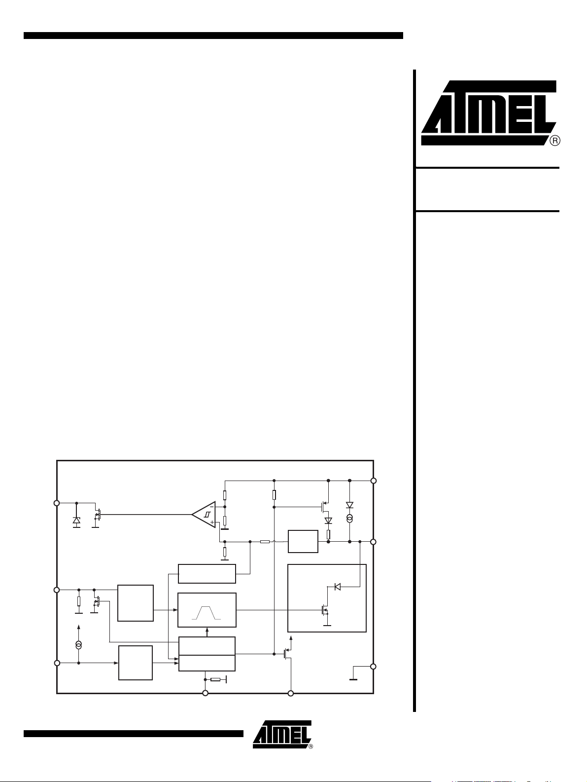
Figure 1-1. Block Diagram
1
RXD
TXD
WAKE
4
VS
3
TXD
time-out
timer
Wake-up
timer
Receiver
Filter
Wake-up bus timer
Slew rate control
Control unit
Standby mode
28
EN
Short circuit and overtemperature protection
VS
INH
7
VS
6
LIN
5
GN
4916E–AUTO–02/07
Page 2
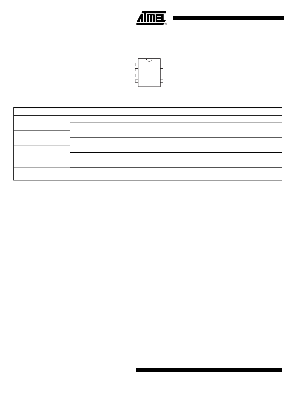
2. Pin Configuration
Figure 2-1. Pinning SO8
INH
RXD
1
EN
2
WAKE
TXD
3
4
Table 2-1. Pin Description
Pin Symbol Function
1 RXD Receive data output (open drain)
2 EN Enables normal mode; when the input is open or low, the device is in sleep mode
3 WAKE High voltage input for local wake-up request
4 TXD Transmit data input; active low output (strong pull-down) after a local wake-up request
5 GND Ground, heat sink
6 LIN LIN bus line input/output
7 VS Battery supply
8INH
Battery-related inhibit output for controlling an external voltage regulator; active high after a wake-up
request
8
VS
7
LIN
6
GND
5
2
ATA6662 [Preliminary]
4916E–AUTO–02/07
Page 3

3. Functional Description
3.1 Supply Pin (VS)
Undervoltage detection is implemented to disable transmission if VS falls to a value below 5V in
order to avoid false bus messages. After switching on V
and INHIBIT is switched on. The supply current in sleep mode is typically 10 µA.
3.2 Ground Pin (GND)
The ATA6662 is neutral on the LIN pin in the case of a GND disconnection. It is able to handle a
ground shift up to 11.5% of V
3.3 Bus Pin (LIN)
A low-side driver with internal current limitation and thermal shutdown and an internal pull-up
resistor are implemented as specified for LIN 2.0. The voltage range is from –27V to +40V. This
pin exhibits no reverse current from the LIN bus to V
disconnection. The LIN receiver thresholds are compatible to the LIN protocol specification.The
fall time (from recessive to dominant) and the rise time (from dominant to recessive) are slope
controlled. The output has a self-adapting short circuit limitation; that is, during current limitation,
as the chip temperature increases, the current is reduced.
ATA6662 [Preliminary]
, the IC switches to pre-normal mode
S
.
S
, even in the case of a GND shift or V
S
Batt
3.4 Input Pin (TXD)
This pin is the microcontroller interface to control the state of the LIN output. TXD is low to bring
LIN low. If TXD is high, the LIN output transistor is turned off. Then, the bus is in recessive mode
via the internal pull-up resistor. The TXD pin is compatible to both a 3.3V or 5V supply.
3.5 TXD Dominant Time-out Function
The TXD input has an internal pull-down resistor. An internal timer prevents the bus line from
being driven permanently in dominant state. If TXD is forced low longer than t
LIN will be switched off (recessive mode). To reset this mode, switch TXD to high (>10 µs)
before switching LIN to dominant again.
3.6 Output Pin (RXD)
This pin reports to the microcontroller the state of the LIN bus. LIN high (recessive) is reported
by a high level at RXD, LIN low (dominant) is reported by a low voltage at RXD. The output is an
open drain, therefore, it is compatible to a 3.3V or 5V power supply. The AC characteristics are
defined with a pull-up resistor of 5 kΩ to 5V and a load capacitor of 20 pF. The output is
short-current protected. In unpowered mode (V
a Zener diode is integrated, with V
=6.1V.
Z
> 6 ms, the pin
dom
= 0V), RXD is switched off. For ESD protection
S
4916E–AUTO–02/07
3
Page 4

3.7 Enable Input Pin (EN)
This pin controls the operation mode of the interface. If EN = 1, the interface is in normal mode,
with the transmission path from TXD to LIN and from LIN to Rx both active. A falling edge on EN
while TXD is already set to high, the device is switched to sleep mode and no transmission is
possible. In sleep mode, the LIN bus pin is connected to V
The device can transmit only after being woken up (see Section 3.8, “Inhibit Output Pin (INH)” ).
During sleep mode the device is still supplied from the battery voltage. The supply current is typically 10 µA. The pin EN provides a pull-down resistor in order to force the transceiver into sleep
mode in case the pin is disconnected.
3.8 Inhibit Output Pin (INH)
This pin is used to control an external switchable voltage regulator having a wake-up input. The
inhibit pin provides an internal switch towards pin V
high-side switch is turned on and the external voltage regulator is activated. When the device is
in sleep mode, the inhibit switch is turned off and disables the voltage regulator.
with a weak pull-up current source.
S
. If the device is in normal mode, the inhibit
S
A wake-up event on the LIN bus or at pin WAKE will switch the INH pin to the V
system power-up (V
R
of the high-side output is < 1 kΩ.
DSon
3.9 Wake-up Input Pin (WAKE)
This pin is a high-voltage input used to wake the device up from sleep mode. It is usually connected to an external switch in the application to generate a local wake-up. If you do not need a
local wake-up in your application, connect pin WAKE directly to pin VS. A pull-up current source
with typically –10 µA is implemented. The voltage threshold for a wake-up signal is 3V below the
VS voltage with an output current of typically –3 µA.
Wake-up events from sleep mode:
•LIN bus
•EN pin
• WAKE pin
Figure 3-1 on page 6, Figure 3-2 on page 7 and Figure 3-3 on page 7 show details of wake-up
operations.
level. After a
S
rises from zero), the pin INH switches automatically to the VS level. The
S
4
ATA6662 [Preliminary]
4916E–AUTO–02/07
Page 5

3.10 Operation Modes
1. Normal mode
2. Sleep mode
3. Pre-normal mode
ATA6662 [Preliminary]
This is the normal transmitting and receiving mode. All features are available.
In this mode the transmission path is disabled and the device is in low power mode.
Supply current from V
WAKE will be detected and will switch the device to pre-normal mode. If EN then
switches to high, normal mode is activated. Input debounce timers at pin WAKE
(T
WAKE
), LIN (T
BUS
motive transients or EMI. In sleep mode the INH pin is left floating. The internal
termination between pin LIN and pin V
case pin LIN is short-circuited to GND. Only a weak pull-up current (typical 10 µA)
between pin LIN and pin V
from the actual level on pin LIN or WAKE, guaranteeing that the lowest power consumption is achievable even in the case of a continuous dominant level on pin LIN or a
continuous LOW on pin WAKE.
At system power-up, the device automatically switches to pre-normal mode. It switches
the INH pin to a high state, to the V
then confirm the normal mode by setting the EN pin to high.
is typically 10 µA. A wake-up signal from the LIN bus or via pin
Batt
) and EN (T
is present. The sleep mode can be activated independently
S
sleep,Tnom
) prevent unwanted wake-up events due to auto-
is disabled to minimize the power dissipation in
S
level. The microcontroller of the application will
S
3.11 Remote Wake-up via Dominant Bus State
A voltage less than the LIN pre-wake detection V
transceiver.
A falling edge at pin LIN, followed by a dominant bus level V
period (T
) and a rising edge at pin LIN results in a remote wake-up request.
BUS
The device switches to pre-normal mode. Pin INH is activated (switches to V
termination resistor is switched on. The remote wake-up request is indicated by a low level at pin
RXD to interrupt the microcontroller (see Figure 3-2 on page 7).
3.12 Local Wake-up via Pin WAKE
A falling edge at pin WAKE, followed by a low level maintained for a certain time period (T
results in a local wake-up request. The wake-up time (T
ing to ISO7637, creates a wake-up. The device switches to pre-normal mode. Pin INH is
activated (switches to V
request is indicated by a low level at pin RXD to interrupt the microcontroller and a strong
pull-down at pin TXD (see Figure 3-3 on page 7). The voltage threshold for a wake-up signal is
3V below the VS voltage with an output current of typical –3 µA. Even in the case of a continuous low at pin WAKE it is possible to switch the IC into sleep mode via a low at pin EN. The IC
will stay in sleep mode for an unlimited time. To generate a new wake up at pin WAKE it needs
first a high signal > 6 µs before a negative edge starts the wake-up filtering time again.
) and the internal termination resistor is switched on. The local wake-up
S
at pin LIN activates the internal LIN
LINL
maintained for a certain time
BUSdom
) and the internal
S
) ensures that no transient, accord-
WAKE
WAKE
),
4916E–AUTO–02/07
5
Page 6

3.13 Wake-up Source Recognition
The device can distinguish between a local wake-up request (pin WAKE) and a remote wake-up
request (dominant LIN bus). The wake-up source can be read on pin TXD in pre-normal mode. If
an external pull-up resistor (typically 5 kΩ) has been added on pin TXD to the power supply of
the microcontroller, a high level indicates a remote wake-up request (weak pull-down at pin
TXD) and a low level indicates a local wake-up request (strong pull-down at pin TXD).
The wake-up request flag (signalled on pin RXD) as well as the wake-up source flag (signalled
on pin TXD) are reset immediately if the microcontroller sets pin EN to high (see Figure 3-2 on
page 7 and Figure 3-3 on page 7).
Figure 3-1. Mode of Operation
3.14 Fail-safe Features
• There are now reverse currents < 15 µA at pin LIN during loss of V
• Pin EN provides a pull-down resistor to force the transceiver into sleep mode if EN is
• Pin RXD is set floating if V
• Pin TXD provides a pull-down resistor to provide a static low if TXD is disconnected.
• The LIN output driver has a current limitation, and if the junction temperature T
• The implemented hysteresis, T
a: VS > 5V
< 5V
b: V
S
c: Bus wake-up event
d: Wake-up from wake switch
b
c
INH: high impedance (INH HS switch OFF)
Sleep Mode
Communication: OFF
or GND; this is optimal
BAT
b
EN = 1
Normal Mode
INH: high (INH HS switch ON)
Communication: ON
Unpowered Mode
= 0V
V
Batt
a
b
INH: high (INH internal high-side switch ON)
EN = 0; after 1 → 0 while TXD = 1
EN = 1
Pre-normal Mode
Communication: OFF
Go to sleep command
Local wake-up event
d
behavior for bus systems where some slave nodes are supplied from battery or ignition.
disconnected.
is disconnected.
BAT
exceeds the
j
thermal shut-down temperature T
, the output driver switches off.
off
, enables the LIN output again after the temperature has
hys
been decreased.
6
ATA6662 [Preliminary]
4916E–AUTO–02/07
Page 7

Figure 3-2. LIN Wake-up Waveform Diagram
Bus wake-up filtering time
(TBUS)
LIN bus
ATA6662 [Preliminary]
INH
RXD
External
voltage
regulator
RXD
Low or floating
High or floating
Off state
Node in sleep state
Figure 3-3. Wake-up from Wake-up Switch
Wake pin
State change
High
Low
Regulator wake-up time delay
Microcontroller start-up
delay time
Normal
Mode
EN High
INH
RXD
TXD
Voltage
regulator
EN
Low or floating
High or floating
TXD weak pull-down resistor
Wake filtering time
T
WAKE
Off state
Node in sleep state
High
TXD strong pull-down
On state
Regulator wake-up time delay
Microcontroller start-up
delay time
HighLow
Weak
pull-down
Node in
operation
EN High
4916E–AUTO–02/07
7
Page 8

4. Absolute Maximum Ratings
Stresses beyond those listed under “Absolute Maximum Ratings” may cause permanent damage to the device. This is a stress rating
only and functional operation of the device at these or any other conditions beyond those indicated in the operational sections of this
specification is not implied. Exposure to absolute maximum rating conditions for extended periods may affect device reliability.
Parameters Symbol Min. Typ. Max. Unit
V
S
- Continuous supply voltage
Wake DC and transient voltage (with 33-kΩ serial resistor)
- Transient voltage due to ISO7637 (coupling 1 nF)
Logic pins (RXD, TXD, EN) –0.3 +5.5 V
LIN
- DC voltage
- Transient voltage due to ISO7637 (coupling 1 nF)
INH
- DC voltage –0.3 +40 V
According to IBEE LIN EMC
Test specification 1.0 following IEC 61000-4-2
- Pin VS, LIN to GND
- Pin WAKE (33 kΩ serial resistor)
ESD HBM following STM5.1
with 1.5 kΩ/100 pF
- Pin VS, LIN, WAKE to GND
- Pin INH to GND
HBM ESD
ANSI/ESD-STM5.1
JESD22-A114
AEC-Q100 (002)
CDM ESD STM 5.3.1 ±750 V
Junction temperature T
Storage temperature T
Thermal shutdown T
Thermal shutdown hysteresis T
j
stg
off
hys
Note: 1. Equivalent to discharge a 100-pF capacitor through a 1.5-kΩ resistor.
–0.3 +40 V
–1
–150
–27
–150
±6
±5
±8
±6
+40
+100
+40
+100
V
V
V
V
KV
KV
KV
KV
±3 KV
–40 +150 °C
–55 +150 °C
150 165 180 °C
5 1020°C
5. Thermal Resistance
Parameters Symbol Min. Typ. Max. Unit
Thermal resistance junction ambient R
Special heat sink at GND (pin 5) on PCB (fused lead
frame to pin 5)
8
ATA6662 [Preliminary]
thJA
R
thJA
80 K/W
145 K/W
4916E–AUTO–02/07
Page 9

ATA6662 [Preliminary]
6. Electrical Characteristics
5V < VS < 27V, Tj = –40°C to +150°C
No. Parameters Test Conditions Pin Symbol Min. Typ. Max. Unit Type*
1V
1.1 DC voltage range nominal 7 V
1.2 Supply current in sleep mode
1.3
1.4
1.5 V
1.6
2 RXD Output Pin (Open Drain)
2.1 Low-level input current
2.2 RXD saturation voltage 5-kΩ pull-up resistor to 5V 1 Vsat
2.3 High-level leakage current
2.4 ESD zener diode I
3 TXD Input Pin
3.1 Low-level voltage input 4 V
3.2 High-level voltage input 4 V
3.3 Pull-down resistor V
3.4 Low-level leakage current V
3.5
4EN Input Pin
4.1 Low-level voltage input 2 V
4.2 High-level voltage input 2 V
4.3 Pull-down resistor V
4.4 Low-level input current V
5 INH Output Pin
5.1 High-level voltage
5.2 High-level leakage current
6 WAKE Pin
6.1 High-level input voltage 3 V
6.2 Low-level input voltage I
6.3 Wake pull-up current V
6.4 High-level leakage current V
*) Type means: A = 100% tested, B = 100% correlation tested, C = Characterized on samples, D = Design parameter
Pin
S
Sleep mode
V
> V
V
lin
Batt
Batt
< 14V
– 0.5V
7I
Bus recessive 7 I
Supply current in normal mode
undervoltage threshold V
S
undervoltage threshold
V
S
hysteresis
Low-level input current at local
wake-up request
Bus dominant
Total bus load > 500Ω
7I
7V
Normal mode
V
LIN
= 0V, V
RXD
= 0.4V
Normal mode
= V
, V
V
LIN
BAT
= 100 µA 1 VZ
RXD
= 5V 4 R
TXD
= 0V 4 I
TXD
RXD
= 5V
Pre-normal mode
V
= V
LIN
EN
EN
; V
BAT
= 5V 2 R
= 0V 2 I
WAKE
= 0V
Normal mode
= –200 µA
I
INH
Sleep mode
= 27V, V
V
INH
= Typically –3 µA 3 V
WAKE
< 27V 3 I
S
= 27V, V
S
= 27V
Batt
= 27V 3 I
WAKE
1I
1I
4I
8V
8I
S
VSstby
VSrec
VSdom
Sth
Sth_hys
RXDL
RXD
RXDH
RXD
TXDL
TXDH
TXD
TXD
TXDwake
ENL
ENH
EN
EN
INHH
INHL
WAKEH
WAKEL
WAKE
WAKE
513.527V A
10 20 µA A
1.6 3 mA A
1.6 3 mA A
44.65 VA
0.2 V A
1.3 2.5 8 mA A
0.4 V A
–3 +3 µA A
5.8 8.6 V A
–0.3 +0.8 V A
27VA
125 250 600 kΩ A
–3 +3 µA A
1.3 2.5 8 mA A
–0.3 +0.8 V A
27VA
125 250 600 kΩ A
–3 +3 µA A
VS – 0.8 V
S
VA
–3 +3 µA A
VS –
1V
–1V
VS +
0.3V
–
V
S
3V
VA
VA
–30 –10 µA A
–5 +5 µA A
4916E–AUTO–02/07
9
Page 10

6. Electrical Characteristics (Continued)
5V < VS < 27V, Tj = –40°C to +150°C
No. Parameters Test Conditions Pin Symbol Min. Typ. Max. Unit Type*
7 LIN Bus Driver
7.1 Driver recessive output voltage R
Driver dominant voltage
7.2
V
BUSdom_DRV_LoSUP
Driver dominant voltage
7.3
V
BUSdom_DRV_HiSUP
Driver dominant voltage
7.4
V
BUSdom_DRV_LoSUP
Driver dominant voltage
7.5
V
BUSdom_DRV_HiSUP
7.6 Pull-up resistor to V
LIN current limitation
7.7
V
= V
BUS
BAT_max
S
Input leakage current at the
7.8
receiver, including pull-up
resistor as specified
= 500Ω/1kΩ 6V
LOAD
V
= 7V, R
VS
V
= 18V, R
VS
V
= 7V, R
VS
V
= 18V, R
VS
The serial diode is
mandatory
= 500Ω 6V
load
= 500Ω 6V
load
= 1000Ω 6V
load
= 1000Ω 6V
load
6R
6I
Input leakage current
Driver off
= 0V, V
V
BUS
Batt
= 12V
6I
BUSrec
_LoSUP
_HiSUP
_LoSUP_1k
_HiSUP_1k_
LIN
BUS_LIM
BUS_PAS_dom
Driver off
≥ V
BAT
BUS
< 18V
< 18V
BAT
6I
BUS_PAS_rec
7.9 Leakage current LIN recessive
8V < V
8V < V
V
BUS
Leakage current at ground loss;
Control unit disconnected from
7.10
ground; Loss of local ground
must not affect communication in
GND
V
=12V
BAT
0V < V
Device
BUS
= V
< 18V
S
6I
BUS_NO_gnd
the residual network
Node has to sustain the current
that can flow under this
7.11
condition; Bus must remain
operational under this condition
disconnected
V
BAT
V
SUP_Device
0V < V
BUS
= GND
< 18V
6I
BUS
8 LIN Bus Receiver
8.1 Center of receiver threshold
8.2 Receiver dominant state V
8.3 Receiver recessive state V
8.4 Receiver input hysteresis V
Pre-wake detection LIN
8.5
High-level input voltage
Pre-wake detection LIN
8.6
Low-level input voltage
V
BUS_CNT
(V
EN
EN
HYS
Switches the LIN receiver
on
th_dom
=
+ V
th_rec
)/2
6V
= 5V 6 V
= 5V 6 V
= V
th_rec
– V
th_dom
6V
6V
6V
BUS_CNT
BUSdom
BUSrec
BUShys
LINH
LINL
*) Type means: A = 100% tested, B = 100% correlation tested, C = Characterized on samples, D = Design parameter
0.9 ×
V
S
V
S
VA
1.2 V A
2VA
0.6 V A
0.8 V A
20 30 60 kΩ A
40 120 200 mA A
–1 mA A
15 20 µA A
–10 +0.5 +10 µA A
515µAA
0.475 ×
–27
0.6 ×
0.028 ×
VS –
–27V
V
V
V
1V
0.5 ×
S
S
0.1 ×
S
0.525
V
× V
S
0.4 ×
V
S
S
VA
VA
40 V A
0.175
V
× V
S
VS +
0.3V
V
S
3.3V
S
–
VA
VA
VA
10
ATA6662 [Preliminary]
4916E–AUTO–02/07
Page 11

ATA6662 [Preliminary]
6. Electrical Characteristics (Continued)
5V < VS < 27V, Tj = –40°C to +150°C
No. Parameters Test Conditions Pin Symbol Min. Typ. Max. Unit Type*
9 Internal Timers
Dominant time for wake-up via
9.1
LIN bus
Time of low pulse for wake-up
9.2
via pin WAKE
Time delay for mode change
9.3
from pre-normal mode to normal
mode via pin EN
Time delay for mode change
9.4
from normal mode into sleep
mode via pin EN
9.5 TXD dominant time out timer V
Power-up delay between
9.6
= 5V until INH switches to
V
S
high
LIN Bus Driver (see Figure 6-1 on page 12)
10
Bus load conditions: Load1, small, 1 nF 1 kΩ; Load2, big, 10 nF 500Ω; R
The following two rows specify the timing parameters for proper operation at 20.0 kBits/s.
10.1 Duty cycle 1
10.2 Duty cycle 2
10.3 Duty cycle 3
10.4 Duty cycle 4
Receiver Electrical AC Parameters of the LIN Physical Layer
11
LIN receiver, RXD load conditions (C
Propagation delay of receiver
11.1
(see Figure 6-1 on page 12)
Symmetry of receiver
11.2
propagation delay rising edge
minus falling edge
*) Type means: A = 100% tested, B = 100% correlation tested, C = Characterized on samples, D = Design parameter
V
= 0V 6 T
LIN
V
= 0V 3 T
WAKE
VEN = 5V 2 T
= 0V 2 T
V
EN
= 0V 4 T
TXD
VVS = 5V T
RXD
TH
TH
Rec(max)
Dom(max)
= 0.744 × V
= 0.581 × V
S
S
VS = 7.0V to 18V
t
= 50 µs
Bit
D1 = t
TH
Rec(min)
TH
Dom(min)
bus_rec(min)
/(2 × t
= 0.422 × V
= 0.284 × V
)
Bit
S
S
VS = 7.0V to 18V
= 50 µs
t
Bit
D2 = t
bus_rec(max)
TH
Rec(max)
TH
Dom(max)
VS = 7.0V to 18V
= 96 µs
t
Bit
D3 = t
bus_rec(min)
TH
Rec(max)
TH
Dom(max)
VS = 7.0V to 18V
t
= 96 µs
Bit
D4 = t
bus_rec(min)
): 20 pF, R
RXD
= max(t
t
rec_pd
VS = 7.0V to 18V
= t
t
rx_sym
VS = 7.0V to 18V
/(2 × t
= 0.778 × V
= 0.616 × V
/(2 × t
= 0.389 × V
= 0.251 × V
/(2 × t
pull-up
, t
rx_pdr
– t
rx_pdr
rx_pdf
Bit
S
S
Bit
S
S
Bit
= 5 kΩ
rx_pdf
)
LIN D3 0.417 A
)
LIN D4 0.590 A
)
)
t
t
rx_sym
BUS
WAKE
norm
sleep
dom
VS
= 5 kΩ; C
30 90 150 µs A
73550µsA
2 7 15 µs A
2 7 12 µs A
6920msA
200 µs A
= 20 pF;
RXD
D1 0.396 A
D2 0.581 A
rx_pd
6µsA
–2 +2 µs A
4916E–AUTO–02/07
11
Page 12

Figure 6-1. Definition of Bus Timing Parameter
TXD
(Input to transmitting node)
VS
(Transceiver supply
of transmitting node)
RXD
(Output of receiving node 1)
THRec(max)
THDom(max)
THRec(min)
THDom(min)
t
rx_pdf(1)
t
Bit
t
Bus_dom(max)
t
Bit
t
Bus_rec(min)
t
Bit
Thresholds of
receiving node 1
LIN Bus Signal
Thresholds of
receiving node 2
t
Bus_dom(min)
t
Bus_rec(max)
t
rx_pdr(1)
RXD
(Output of receiving node 2)
t
rx_pdr(2)
t
rx_pdf(2)
12
ATA6662 [Preliminary]
4916E–AUTO–02/07
Page 13

Figure 6-2. Application Circuit
ATA6662 [Preliminary]
Master node
pull-up
VBATTERY
22 µF
10 kΩ
External
switch
12V
5V
VDD
Microcontroller
SCI
IO
33 kΩ
RXD
TXD
WAKE
5 kΩ
1
4
3
ATA6662
V
S
TXD
Time-out
timer
Wake-up
timer
Receiver
Wake-up bus timer
Slew rate control
Control unit
Standby mode
2
EN
100 nF
Filter
Short circuit and
overtemperature
protection
V
S
8
INH
1k
7
VS
LIN sub bus
6
LIN
220 pF
5
GND
4916E–AUTO–02/07
13
Page 14

7. Ordering Information
Extended Type Number Package Remarks
ATA6662-TAQY SO8 LIN transceiver, Pb-free
8. Package Information
Package SO8
Dimensions in mm
0.4
5.00
4.85
1.4
0.25
1.27
3.81
85
14
0.10
5.2
4.8
3.7
3.8
6.15
5.85
technical drawings
according to DIN
specifications
0.2
14
ATA6662 [Preliminary]
4916E–AUTO–02/07
Page 15

9. Revision History
Please note that the following page numbers referred to in this section refer to the specific revision
mentioned, not to this document.
Revision No. History
4916E-AUTO-02/07
4916D-AUTO-02/07
ATA6662 [Preliminary]
• Section 4 “Absolute Maximum Ratings” on page 8 changed
• Section 2 “Electrical Characteristics” on pages 9 to 11 changed
• Features on page 1 changed
• Section 1 “Description” on page 1 changed
• Table 2-1 “Pin Description” on page 2 changed
• Section 3.2 “Ground Pin (GND) on page 3 changed
• Section 3.7 “Enable Input Pin (EN)” on page 4 changed
• Section 3.11 “Remote Wake-up via Dominat Bus State” on page 5
changed
• Figure 3-1 “Mode of Operation” on page 6 changed
• Section 3-14 “Fail-safe Features” on page 6 changed
• Section 4 “Absolute Maximum Ratings” on page 8 changed
• Section 6 “Electrical Characteristics” on pages 9 to 11 changed
4916E–AUTO–02/07
15
Page 16

Atmel Corporation Atmel Operations
2325 Orchard Parkway
San Jose, CA 95131, USA
Tel: 1(408) 441-0311
Fax: 1(408) 487-2600
Regional Headquarters
Europe
Atmel Sarl
Route des Arsenaux 41
Case Postale 80
CH-1705 Fribourg
Switzerland
Tel: (41) 26-426-5555
Fax: (41) 26-426-5500
Asia
Room 1219
Chinachem Golden Plaza
77 Mody Road Tsimshatsui
East Kowloon
Hong Kong
Tel: (852) 2721-9778
Fax: (852) 2722-1369
Japan
9F, Tonetsu Shinkawa Bldg.
1-24-8 Shinkawa
Chuo-ku, Tokyo 104-0033
Japan
Tel: (81) 3-3523-3551
Fax: (81) 3-3523-7581
Memory
2325 Orchard Parkway
San Jose, CA 95131, USA
Tel: 1(408) 441-0311
Fax: 1(408) 436-4314
Microcontrollers
2325 Orchard Parkway
San Jose, CA 95131, USA
Tel: 1(408) 441-0311
Fax: 1(408) 436-4314
La Chantrerie
BP 70602
44306 Nantes Cedex 3, France
Tel: (33) 2-40-18-18-18
Fax: (33) 2-40-18-19-60
ASIC/ASSP/Smart Cards
Zone Industrielle
13106 Rousset Cedex, France
Tel: (33) 4-42-53-60-00
Fax: (33) 4-42-53-60-01
1150 East Cheyenne Mtn. Blvd.
Colorado Springs, CO 80906, USA
Tel: 1(719) 576-3300
Fax: 1(719) 540-1759
Scottish Enterprise Technology Park
Maxwell Building
East Kilbride G75 0QR, Scotland
Tel: (44) 1355-803-000
Fax: (44) 1355-242-743
RF/Automotive
Theresienstrasse 2
Postfach 3535
74025 Heilbronn, Germany
Tel: (49) 71-31-67-0
Fax: (49) 71-31-67-2340
1150 East Cheyenne Mtn. Blvd.
Colorado Springs, CO 80906, USA
Tel: 1(719) 576-3300
Fax: 1(719) 540-1759
Biometrics
Avenue de Rochepleine
BP 123
38521 Saint-Egreve Cedex, France
Tel: (33) 4-76-58-47-50
Fax: (33) 4-76-58-47-60
Literature Requests
www.atmel.com/literature
Disclaimer: The information in this document is provided in connection with Atmel products. No license, express or implied, by estoppel or otherwise, to any
intellectual property right is granted by this document or in connection with the sale of Atmel products. EXCEPT AS SET FORTH IN ATMEL’S TERMS AND CONDI-
TIONS OF SALE LOCATED ON ATMEL’S WEB SITE, ATMEL ASSUMES NO LIABILITY WHATSOEVER AND DISCLAIMS ANY EXPRESS, IMPLIED OR STATUTORY
WARRANTY RELATING TO ITS PRODUCTS INCLUDING, BUT NOT LIMITED TO, THE IMPLIED WARRANTY OF MERCHANTABILITY, FITNESS FOR A PARTICULAR
PURPOSE, OR NON-INFRINGEMENT. IN NO EVENT SHALL ATMEL BE LIABLE FOR ANY DIRECT, INDIRECT, CONSEQUENTIAL, PUNITIVE, SPECIAL OR INCIDENTAL DAMAGES (INCLUDING, WITHOUT LIMITATION, DAMAGES FOR LOSS OF PROFITS, BUSINESS INTERRUPTION, OR LOSS OF INFORMATION) ARISING OUT
OF THE USE OR INABILITY TO USE THIS DOCUMENT, EVEN IF ATMEL HAS BEEN ADVISED OF THE POSSIBILITY OF SUCH DAMAGES. Atmel makes no
representations or warranties with respect to the accuracy or completeness of the contents of this document and reserves the right to make changes to specifications
and product descriptions at any time without notice. Atmel does not make any commitment to update the information contained herein. Unless specifically provided
otherwise, Atmel products are not suitable for, and shall not be used in, automotive applications. Atmel’s products are not intended, authorized, or warranted for use
as components in applications intended to support or sustain life.
© 2007 Atmel Corporation. All rights reserved. Atmel®, logo and combinations thereof, Everywhere You Are® and others are registered trade-
marks or trademarks of Atmel Corporation or its subsidiaries. Other terms and product names may be trademarks of others.
4916E–AUTO–02/07
 Loading...