

Page 1
Features
• Supply Voltage up to 40V
• Operating Voltage V
• Typically 10 µA Supply Current During Sleep Mode
• Typically 40 µA Supply Current in Silent Mode
• Linear Low-drop Voltage Regulator:
– Normal, Fail-safe, and Silent Mode
– ATA6629: V
– ATA6631: VCC = 5.0V ±2%
– Sleep Mode: V
• V
Undervoltage Detection with Reset Open Drain Output NRES (4 ms Reset Time)
CC
• Voltage Regulator is Short-circuit and Over-temperature Protected
• LIN Physical Layer According to LIN 2.0, 2.1 and SAEJ2602-2
• Wake-up Capability via LIN Bus (90 µs Dominant)
• TXD Time-out Timer
• Bus Pin is Overtemperature and Short-circuit Protected versus GND and Battery
• Advanced EMC and ESD Performance
• ESD HBM 8 kV at Pins LIN and VS Following STM5.1
• Interference and Damage Protection According to ISO/CD7637
• Package: SO8
= 5V to 27V
S
= 3.3V ±2%
CC
is Switched Off
CC
LIN Bus
Transceiver
with Integrated
Voltage
Regulator
ATA6629
1. Description
ATA6629/ATA6631 is a fully integrated LIN transceiver, designed according to the LIN
specification 2.0, 2.1 and SAEJ2602-2, with a low-drop voltage regulator
(3.3V/5V/50 mA). The combination of voltage regulator and bus transceiver makes it
possible to develop simple, but powerful, slave nodes in LIN Bus systems.
ATA6629/ATA6631 is designed to handle the low-speed data communication in vehicles (for example, in convenience electronics). Improved slope control at the LIN
driver ensures secure data communication up to 20 kBaud with an RC oscillator for
the protocol handling. The bus output is designed to withstand high voltage. Sleep
Mode (voltage regulator switched off) and Silent Mode (communication off; V
age on) guarantee minimized current consumption.
CC
volt-
ATA6631
9165A–AUTO–11/09
Page 2
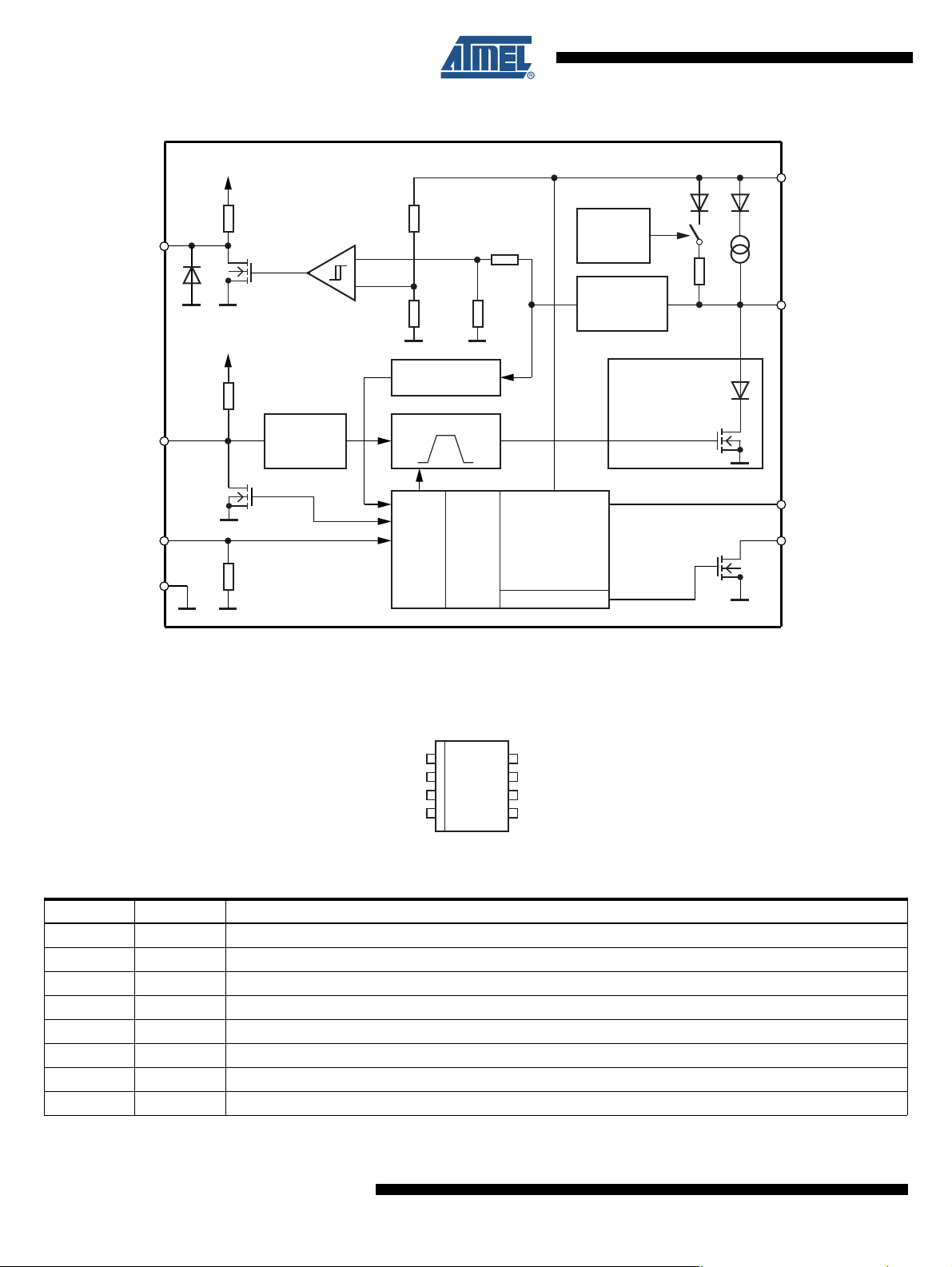
Figure 1-1. Block Diagram
3
GND
2
EN
6
TXD
5
RXD
VCC
8
NRES
7
Short-circuit and
overtemperature
protection
Normal/Silent/
Fail-safe Mode
3.3V/50 mA/±2%
5V/50 mA/±2%
Control
unit
Normal and
Fail-safe
Mode
RF-filter
LIN
VS1
4
TXD
Time-out
timer
Slew rate control
Undervoltage reset
Sleep
mode
VCC
switched
off
Wake-up bus timer
ATA6629/ATA6631
Receiver
V
CC
-
+
V
CC
5 kΩ
VCC
3
4
2
1
TXD
NRES
RXD
VS 8
7
6
5
GND
EN
LIN
2. Pin Configuration
Figure 2-1. Pinning SO8
Table 2-1. Pin Description
2
Pin Symbol Function
1 VS Battery supply
2 EN Enables Normal Mode if the input is high
3 GND Ground, heat sink
4 LIN LIN bus line input/output
5 RXD Receive data output
6 TXD Transmit data input
7 NRES Output undervoltage reset, low at reset
8 VCC Output voltage regulator 3.3V/5V/50 mA
ATA6629/ATA6631
9165A–AUTO–11/09
Page 3

3. Functional Description
3.1 Physical Layer Compatibility
Since the LIN physical layer is independent from higher LIN layers (e.g., LIN protocol layer), all
nodes with a LIN physical layer according to revision 2.x can be mixed with LIN physical layer
nodes, which are according to older versions (i.e., LIN 1.0, LIN 1.1, LIN 1.2, LIN 1.3) without any
restrictions.
3.2 Supply Pin (VS)
LIN operating voltage is VS= 5V to 27V. An undervoltage detection is implemented to disable
transmission if V
the IC starts with the Fail-safe Mode and the voltage regulator is switched on (i.e.,
3.3V/5V/50 mA).
The supply current in Sleep Mode is typically 10 µA and 40 µA in Silent Mode.
3.3 Ground Pin (GND)
The IC is neutral on the LIN pin in the event of GND disconnection. It is able to handle a ground
shift up to 11.5% of V
ATA6629/ATA6631
falls below 5V, in order to avoid false bus messages. After switching on VS,
S
.
S
3.4 Voltage Regulator Output Pin (VCC)
The internal 3.3V/5V voltage regulator is capable of driving loads with up to 50 mA, supplying
the microcontroller and other ICs on the PCB and is protected against overload by means of current limitation and overtemperature shut-down. Furthermore, the output voltage is monitored
and will cause a reset signal at the NRES output pin if it drops below a defined threshold V
3.5 Undervoltage Reset Output (NRES)
If the VCC voltage falls below the undervoltage detection threshold V
after tres_f (Figure 6-1 on page 14). Even if V
nally driven from the V
voltage. If VS voltage ramps down, NRES stays low until VS< 1.5V and
S
then becomes highly resistant.
The implemented undervoltage delay keeps NRES low for t
nominal value.
3.6 Bus Pin (LIN)
A low-side driver with internal current limitation and thermal shutdown as well as an internal
pull-up resistor according to LIN specification 2.x is implemented. The voltage range is from
–27V to +40V. This pin exhibits no reverse current from the LIN bus to V
GND shift or V
col specification.
The fall time (from recessive to dominant) and the rise time (from dominant to recessive) are
slope controlled.
disconnection. The LIN receiver thresholds are compatible with the LIN proto-
Batt
, NRES switches to low
thun
= 0V the NRES stays low, because it is inter-
CC
= 4 ms after VCC reaches its
Reset
, even in the event of a
S
thun
.
9165A–AUTO–11/09
3
Page 4

3.7 Input/Output (TXD)
In Normal Mode the TXD pin is the microcontroller interface to control the state of the LIN output.
TXD must be pulled to ground in order to drive the LIN bus low. If TXD is high or unconnected
(internal pull-up resistor), the LIN output transistor is turned off and the bus is in the recessive
state. During Fail-safe Mode, this pin is used as output and is signalling the fail-safe source.
3.8 Dominant Time-out Function (TXD)
The TXD input has an internal pull-up resistor. An internal timer prevents the bus line from being
driven permanently in the dominant state. If TXD is forced to low longer than t
LIN bus driver is switched to the recessive state. Nevertheless, when switching to Sleep Mode,
the actual level at the TXD pin is relevant.
To reactivate the LIN bus driver, switch TXD to high (> 10 µs).
3.9 Output Pin (RXD)
This pin reports the state of the LIN bus to the microcontroller. LIN high (recessive state) is
reported by a high level at RXD; LIN low (dominant state) is reported by a low level at RXD. The
output has an internal pull-up resistor with typically 5 kΩ to V
sured with an external load capacitor of 20 pF.
>27ms, the
DOM
. The AC characteristics are mea-
CC
The output is short-circuit protected. In Unpowered Mode (that is, V
3.10 Enable Input Pin (EN)
The Enable Input pin controls the operation mode of the device. If EN is high, the circuit is in
Normal Mode, with transmission paths from TXD to LIN and from LIN to RXD both active. The
VCC voltage regulator operates with 3.3V/5V/50 mA output capability.
If EN is switched to low while TXD is still high, the device is forced to Silent Mode. No data transmission is then possible, and the current consumption is reduced to I
regulator has its full functionality.
If EN is switched to low while TXD is low, the device is forced to Sleep Mode. No data transmission is possible, and the voltage regulator is switched off.
= 0V), RXD is switched off.
S
typ. 40 µA. The VCC
VS
4
ATA6629/ATA6631
9165A–AUTO–11/09
Page 5
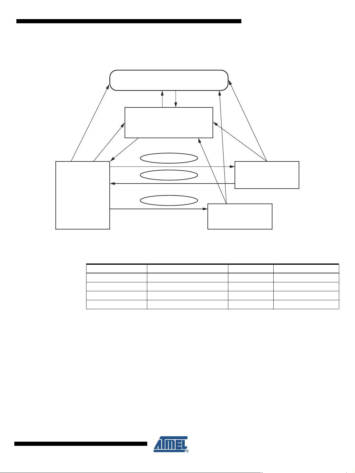
4. Mode of Operation
Unpowered Mode
(See section 4.5)
a: V
S
> VS
thF
b: VS < VS
thU
c: Bus wake-up event
d: NRES switches to low
Fail-safe Mode
Normal Mode
VCC: 3.3V/5V/50 mA
with undervoltage
monitoring
Communication: ON
VCC: 3.3V/5V/50 mA
with undervoltage monitoring
Communication: OFF
Silent Mode
VCC: 3.3V/5V/50 mA
with undervoltage monitoring
Communication: OFF
Sleep Mode
VCC: switched off
Communication: OFF
Go to silent command
a
TXD = 0
EN = 0
TXD = 1
EN = 0
EN = 1
EN = 1
EN = 1
b
b
b
c + d
d
c
b
Local wake-up event
Go to sleep command
Figure 4-1. Mode of Operation
ATA6629/ATA6631
9165A–AUTO–11/09
Table 4-1. Mode of Operation
Mode of Operation Transceiver V
Fail safe OFF 3.3V/5V Recessive
Normal ON 3.3V/5V TXD depending
Silent OFF 3.3V/5V Recessive
Sleep OFF 0V Recessive
CC
LIN
5
Page 6

4.1 Normal Mode
4.2 Silent Mode
This is the normal transmitting and receiving mode of the LIN Interface, in accordance with LIN
specification 2.x. The V
voltage regulator operates with a 3.3V/5V output voltage, with a low
CC
tolerance of ±2% and a maximum output current of 50 mA.
If an undervoltage condition occurs, NRES is switched to low and the IC changes its state to
Fail-safe Mode.
A falling edge at EN while TXD is high switches the IC into Silent Mode. The TXD Signal has to
be logic high during the Mode Select window (Figure 4-3 on page 7). The transmission path is
disabled in Silent Mode. The overall supply current from V
I
= 40 µA plus the VCC regulator output current I
VSsi
VCCs
.
is a combination of the
Batt
Figure 4-2. Switch to Silent Mode
Normal Mode
EN
TXD
NRES
VCC
LIN
Mode select window
= 3.2 µs
t
d
Delay time silent mode
t
_silent = maximum 20 µs
d
LIN switches directly to recessive mode
Silent Mode
The 3.3V/5V regulator with 2% tolerance can source up to 50 mA. In Silent Mode the internal
slave termination between pin LIN and pin VS is disabled to minimize the current consumption in
case pin LIN is short-circuited to GND. Only a weak pull-up current (typically 10 µA) between pin
LIN and pin VS is present. The Silent Mode can be activated independently from the current
level on pin LIN.
If an undervoltage condition occurs, NRES is switched to low and the ATA6629/ATA6631
changes its state to Fail-safe Mode.
6
ATA6629/ATA6631
9165A–AUTO–11/09
Page 7
ATA6629/ATA6631
A voltage less than the LIN Pre-wake detection V
at pin LIN activates the internal LIN
LINL
receiver and starts the wake-up detection timer.
A falling edge at the LIN pin followed by a dominant bus level maintained for a certain time
period (t
) and the following rising edge at pin LIN (see Figure 4-3 on page 7) results in a
bus
remote wake-up request. The device switches from Silent Mode to Fail-safe Mode, then the
internal LIN slave termination resistor is switched on. The remote wake-up request is indicated
by a low level at pin RXD and TXD to interrupt the microcontroller (Figure 4-3 on page 7). EN
high can be used to switch directly to Normal Mode.
Figure 4-3. LIN Wake-up Waveform Diagram from Silent Mode
Bus wake-up filtering time
LIN bus
RXD
t
bus
High
Fail-safe mode Normal mode
Low
VCC
EN
NRES
HighTXD
Silent mode 3.3V/5V/50 mA Fail-safe mode 3.3V/5V/50 mA
Undervoltage detection active
High
Normal mode
EN High
9165A–AUTO–11/09
7
Page 8
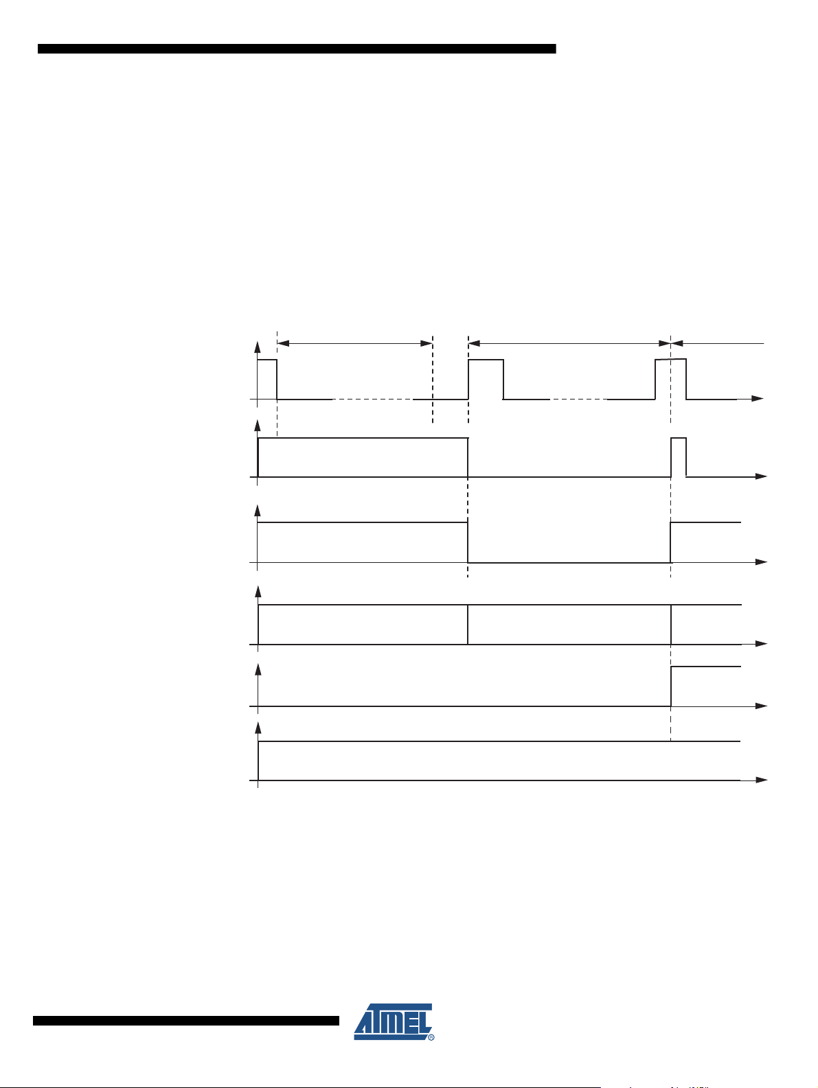
4.3 Sleep Mode
Delay time sleep mode
t
d_sleep
= maximum 20 µs
LIN switches directly to recessive mode
t
d
= 3.2 µs
LIN
VCC
NRES
TXD
EN
Sleep Mode
Normal Mode
Mode select window
A falling edge at EN while TXD is low switches the IC into Sleep Mode. The TXD Signal has to
be logic low during the Mode Select window (Figure 4-5 on page 9).
Figure 4-4. Switch to Sleep Mode
In order to avoid any influence to the LIN-pin during switching into sleep mode it is possible to
switch the EN up to 3.2 µs earlier to Low than the TXD. Therefore, the best an easiest way are
two falling edges at TXD and EN at the same time.
In Sleep Mode the transmission path is disabled. Supply current from V
I
=10µA. The VCC regulator is switched off; NRES and RXD are low. The internal slave
VSsleep
is typically
Batt
termination between pin LIN and pin VS is disabled to minimize the current consumption in case
pin LIN is short-circuited to GND. Only a weak pull-up current (typically 10 µA) between pin LIN
and pin VS is present. The Sleep Mode can be activated independently from the current level on
pin LIN.
8
ATA6629/ATA6631
9165A–AUTO–11/09
Page 9

ATA6629/ATA6631
Regulator wake-up time
Off state
On state
Low
Fail-safe Mode Normal Mode
EN High
Microcontroller
start-up time delay
Reset
time
Low or floating
Low or floating
NRES
EN
VCC
voltage
regulator
RXD
LIN bus
Bus wake-up filtering time
t
bus
High
TXD
A voltage less than the LIN Pre-wake detection V
at pin LIN activates the internal LIN
LINL
receiver and starts the wake-up detection timer.
A falling edge at the LIN pin followed by a dominant bus level maintained for a certain time
period (t
) and a following rising edge at pin LIN results in a remote wake-up request. The
bus
device switches from Sleep Mode to Fail-safe Mode.
The V
regulator is activated, and the internal LIN slave termination resistor is switched on. The
CC
remote wake-up request is indicated by a low level at RXD and TXD to interrupt the microcontroller (Figure 4-5 on page 9).
EN high can be used to switch directly from Sleep/Silent to Fail-safe Mode. If EN is still high after
VCC ramp up and undervoltage reset time, the IC switches to Normal Mode.
Figure 4-5. LIN Wake-up Diagram from Sleep Mode
9165A–AUTO–11/09
9
Page 10

4.4 Sleep or Silent Mode: Behavior at a Floating LIN-bus or a Short Circuited LIN to GND
In Sleep or in Silent Mode the device has a very low current consumption even during shortcircuits or floating conditions on the bus. A floating bus can arise if the Master pull-up resistor is
missing, e.g., if it is switched off when the LIN- Master is in sleep mode or even if the power
supply of the Master node is switched off.
In order to minimize the current consumption I
in sleep or silent mode during voltage levels at
VS
the LIN-pin below the LIN pre-wake threshold, the receiver is activated only for a specific time
tmon. If t
elapses while the voltage at the bus is lower than Pre-wake detection low (V
mon
LINL
and higher than the LIN dominant level, the receiver is switched off again and the circuit
changes back to sleep respectively Silent Mode. The current consumption is then the result of
I
or I
VSsleep
Even if the voltage rises above the Pre-wake detection high (V
VSsilent
plus I
. If a dominant state is reached on the bus no wake-up will occur.
LINwake
), the IC will stay in sleep
LINH
respectively silent mode (see Figure 4-6).
This means the LIN-bus must be above the Pre-wake detection threshold V
for a few micro-
LINH
seconds before a new LIN wake-up is possible.
Figure 4-6. Floating LIN-bus During Sleep or Silent Mode
LIN Pre-wake
V
LIN BUS
LINL
V
BUSdom
t
mon
LIN dominant state
)
10
I
VS
Mode of
operation
Int. Pull-up
Resistor
RLIN
I
Sleep/Silent Mode Sleep/Silent Mode
If the ATA6629/ATA6631 is in Sleep or Silent Mode and the voltage level at the LIN-bus is in
dominant state (V
example), the IC switches back to Sleep Mode respectively Silent Mode. The V
consumption then consists of I
IC switches directly to Fail-safe Mode (see Figure 4-7 on page 11).
ATA6629/ATA6631
VSsleep/silent
< V
LIN
BUSdom
I
VSfail
Wake-up Detection Phase
off (disabled)
) for a time period exceeding t
VSsleep
or I
VSsilent
plus I
LINWAKE
I
VSsleep
+ I
LINwake
I
VSsleep
(during a short circuit at LIN, for
mon
current
S
. After a positive edge at pin LIN the
9165A–AUTO–11/09
Page 11

ATA6629/ATA6631
Sleep/Silent
Mode
I
VSsleep/silent
I
VSfail
+ I
LINwake
I
VSsleep/silent
V
BUSdom
V
LINL
LIN Pre-wake
LIN dominant state
LIN BUS
I
VS
Mode of
operation
Int. Pull-up
Resistor
RLIN
off (disabled) on (enabled)
Wake-up Detection PhaseSleep/Silent Mode Fail-Safe Mode
t
mon
t
mon
Figure 4-7. Short Circuit to GND on the LIN bus During Sleep- or Silent Mode
4.5 Fail-safe Mode
9165A–AUTO–11/09
The device automatically switches to Fail-safe Mode at system power-up. The voltage regulator
is switched on (V
switches to low for t
= 3.3V/5V/2%/50 mA) (see Figure 6-1 on page 14). The NRES output
CC
= 4 ms and gives a reset to the microcontroller. LIN communication is
res
switched off. The IC stays in this mode until EN is switched to high. The IC then changes to Normal Mode. A power down of V
Fail-safe Mode after power up. A low at NRES switches the IC into Fail-safe Mode directly. Dur-
(VS<VSth) during Silent or Sleep Mode switches the IC into
Batt
ing Fail-safe Mode the TXD pin is an output and signals the fail-safe source.
The LIN SBC can operate in different Modes, like Normal, Silent or Sleep Mode. The functionality of these Modes is described in Table 4-2.
Table 4-2. TXD, RXD Depending from Operation Modes
11
Different Modes TXD RXD
Fail-safe Mode Signalling fail-safe sources (see Table 4-3)
Normal Mode Follows data transmission
Silent and Sleep Mode High High
Page 12

A wake-up event from either Silent or Sleep Mode will be signalled to the microcontroller using
the two pins RXD and TXD. The coding is shown in Table 4-3.
A wake-up event will lead the IC to the Fail-safe Mode.
Table 4-3. Signalling Fail-safe Sources
Fail-safe Sources TXD RXD
LIN wake up (pin LIN) Low Low
VS
4.6 Unpowered Mode
If you connect battery voltage to the application circuit, the voltage at the VS pin increases
according to the block capacitor (see Figure 6-1 on page 14). After VS is higher than the VS
undervoltage threshold VS
The VCC output voltage reaches its nominal value after t
VCC capacitor and the load.
(battery) undervoltage detection High Low
th
, the IC mode changes from Unpowered Mode to Fail-safe Mode.
th
. This time, t
VCC
, depends on the
VCC
The NRES is low for the reset time delay t
. During this time, t
reset
possible.
IF VS drops below VS
, then the IC switches to Unpowered Mode. The behaviour of VCC,
th
NRES and LIN is shown in Figure 4-8.
Figure 4-8. VCC versus VS for the VCC = 3.3V Regulator
6.0
5.5
5.0
4.5
4.0
3.5
3.0
V in V
2.5
2.0
1.5
1.0
0.5
0.0
0.0 0.5 1.0 1.5 2.0 2.5 3.0 3 .5 4 .0 4 .5 5.0 5.5 6 .0
Regulator drop voltage V
VS
D
VCC
VS in V
NRES
, no mode change is
reset
LIN
12
ATA6629/ATA6631
9165A–AUTO–11/09
Page 13

5. Fail-safe Features
ATA6629/ATA6631
• During a short-circuit at LIN to V
the power dissipation, the chip temperature exceeds T
The chip cools down and after a hysteresis of T
on high because LIN is high. During LIN overtemperature switch-off, the V
, the output limits the output current to I
Battery
and the LIN output is switched off.
LINoff
, switches the output on again. RXD stays
hys
BUS_LIM
regulator is
CC
. Due to
working independently.
• During a short-circuit from LIN to GND the IC can be switched into Sleep or Silent Mode and
even in this case the current consumption is lower than 45 µA in Sleep Mode and lower than
80 µA in Silent Mode. If the short-circuit disappears, the IC starts with a remote wake-up.
• Sleep or Silent Mode: During a floating condition on the bus the IC switches back to Sleep
Mode/Silent Mode automatically and thereby the current consumption is lower than
45 µA/80 µA.
• The reverse current is < 2 µA at pin LIN during loss of V
. This is optimal behavior for bus
Batt
systems where some slave nodes are supplied from battery or ignition.
• During a short circuit at VCC, the output limits the output current to I
. Because of
VCClim
undervoltage, NRES switches to low and sends a reset to the microcontroller. The IC
switches into Fail-safe Mode. If the chip temperature exceeds the value T
output switches off. The chip cools down and after a hysteresis of T
again. Because of Fail-safe Mode, the V
voltage will switch on again although EN is
CC
, switches the output on
hys
VCCoff
, the VCC
switched off from the microcontroller.The microcontroller can then start with normal
operation.
• Pin EN provides a pull-down resistor to force the transceiver into Recessive Mode if EN is
disconnected.
• Pin RXD is set floating if V
is disconnected.
Batt
• Pin TXD provides a pull-up resistor to force the transceiver into Recessive Mode if TXD is
disconnected.
• If TXD is short-circuited to GND, it is possible to switch to Sleep Mode via ENABLE after
t>tdom.
9165A–AUTO–11/09
13
Page 14

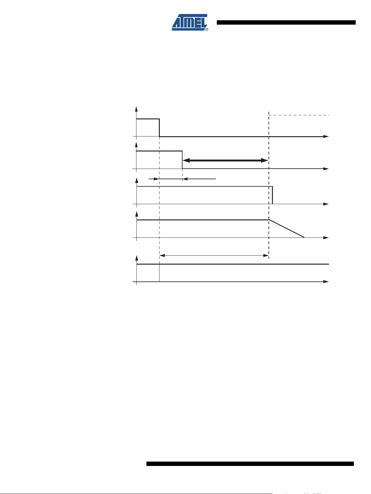
6. Voltage Regulator
Figure 6-1. VCC Voltage Regulator: Ramp Up and Undervoltage
VS
12V
5.5V/3.8V
VCC
5V/3.3V
V
thun
t
res_f
NRES
5V/3.3V
t
VCC
t
Reset
The voltage regulator needs an external capacitor for compensation and to smooth the disturbances from the microcontroller. It is recommended to use an electrolytic capacitor with
C > 1.8 µF and a ceramic capacitor with C = 100 nF. The values of these capacitors can be varied by the customer, depending on the application.
With this special SO8 package (fused lead frame to pin 3) an R
of 80 K/W is achieved.
thja
Therefore, it is recommended to connect pin 3 with a wide GND plate on the printed board to get
a good heat sink.
The main power dissipation of the IC is created from the V
output current I
CC
, which is
VCC
needed for the application.
Figure 6-2 shows the safe operating area of the ATA6629/ATA6631.
14
ATA6629/ATA6631
9165A–AUTO–11/09
Page 15

ATA6629/ATA6631
0.00
8 9 10111213 14 15 18 1916 17567
10.00
20.00
30.00
40.00
50.00
60.00
T
amb
= 85°C
T
amb
= 105°C
T
amb
= 95°C
VS (V)
I
VCC
(mA)
Figure 6-2. Power Dissipation: Save Operating Area versus VCC Output Current and Supply
Voltage V
at Different Ambient Temperatures Due to R
S
= 80 K/W
thja
For programming purposes of the microcontroller, it is potentionally necessary to supply the V
CC
output via an external power supply while the VS Pin of the system basis chip is disconnected.
This behavior is no problem for the system basis chip.
9165A–AUTO–11/09
15
Page 16

7. Absolute Maximum Ratings
Stresses beyond those listed under “Absolute Maximum Ratings” may cause permanent damage to the device. This is a stress rating
only and functional operation of the device at these or any other conditions beyond those indicated in the operational sections of this
specification is not implied. Exposure to absolute maximum rating conditions for extended periods may affect device reliability.
Parameters Symbol Min. Typ. Max. Unit
Supply voltage V
S
V
S
Pulse time ≤ 500 ms
=25°C
T
a
Output current I
VCC
≤ 50 mA
V
S
Pulse time ≤ 2min
T
=25°C
a
Output current I
VCC
≤ 50 mA
V
S
Logic pins (RxD, TxD, EN, NRES) –0.3 +5.5 V
Output current NRES I
NRES
LIN
- DC voltage –27 +40 V
V
CC
- DC voltage –0.3 +5.5 V
ESD according to IBEE LIN EMC
Test specification 1.0 following IEC 61000-4-2
- Pin VS, LIN to GND ±6 KV
ESD HBM following STM5.1
with 1.5 kΩ/100 pF
- Pin VS, LIN to GND ±8 KV
HBM ESD
ANSI/ESD-STM5.1
JESD22-A114
AEC-Q100 (002)
CDM ESD STM 5.3.1 ±750 V
Machine Model ESD
AEC-Q100-RevF(003)
Junction temperature T
Storage temperature T
j
s
–0.3 +40 V
+40 V
27 V
+2 mA
±3 KV
±200 V
–40 +150 °C
–55 +150 °C
8. Thermal Characteristics
Parameters Symbol Min. Typ. Max. Unit
Thermal resistance junction to ambient
(free air)
Special heat sink at GND (pin 3) on PCB R
Thermal shutdown of V
regulator T
CC
Thermal shutdown of LIN output T
Thermal shutdown hysteresis T
16
ATA6629/ATA6631
R
thja
thja
VCCoff
LINoff
hys
80 K/W
150 160 170 °C
150 160 170 °C
10 °C
145 K/W
9165A–AUTO–11/09
Page 17

ATA6629/ATA6631
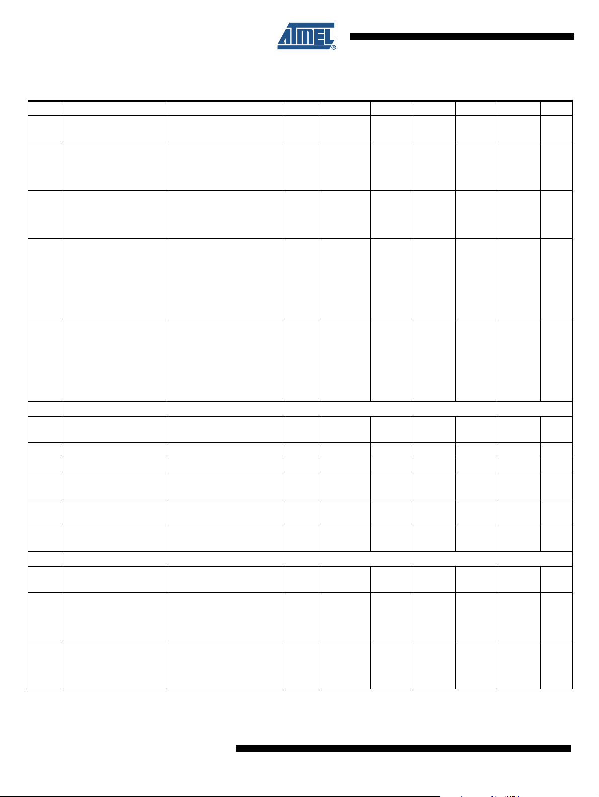
9. Electrical Characteristics
5V < VS < 27V, –40°C < Tj < 150°C; unless otherwise specified all values refer to GND pins.
No. Parameters Test Conditions Pin Symbol Min. Typ. Max. Unit Type*
1VS Pin
Nominal DC voltage
1.1
range
VS V
S
Sleep Mode
V
> VS – 0.5V
LIN
VS I
VSsleep
VS < 14V (Tj = 25°C)
Supply current in Sleep
1.2
Mode
Sleep Mode
> VS – 0.5V
V
LIN
VS < 14V (Tj = 125°C)
VS I
VSsleep
Sleep Mode
bus shorted to GND
= 0V, VS < 14V
V
LIN
VS I
VSsleep_sc
Bus recessive
V
< 14V (Tj = 25°C)
S
VS I
VSsi
Without load at VCC
Bus recessive
Supply current in Silent
1.3
Mode
< 14V (Tj = 125°C)
V
S
Without load at VCC
VS I
VSsi
Silent Mode
bus shorted to GND
= 0V, VS < 14V,
V
LIN
VS I
VSsleep_sc
without load at VCC
Supply current in Normal
1.4
Mode
Supply current in Normal
1.5
Mode
Supply current in
1.6
Fail-safe Mode
VS undervoltage
1.7
threshold
VS undervoltage
1.8
hysteresis
Bus recessive
V
< 14V
S
VS I
Without load at VCC
Bus dominant
< 14V
V
S
load current 50 mA
V
CC
VS I
Bus recessive
V
< 14V
S
VS I
Without load at VCC
Switch to Unpowered Mode VS V
Switch to Fail-safe Mode VS V
VS V
VSrec
VSdom
VSfail
SthU
SthF
Sth_hys
2 RXD Output Pin
Low level output sink
2.1
current
2.2 Low level output voltage I
2.3 Internal resistor to V
Normal Mode
V
=0V, V
LIN
= 1 mA RXD V
RXD
RXD R
CC
RXD
=0.4V
RXD I
RXD
RXDL
RXD
3 TXD Input/Output Pin
3.1 Low level voltage input TXD V
3.2 High level voltage input TXD V
3.3 Pull-up resistor V
=0V TXD R
TXD
TXDL
TXDH
TXD
*) Type means: A = 100% tested, B = 100% correlation tested, C = Characterized on samples, D = Design parameter
513.527 VA
31014µAA
51116µAA
23 45 µA A
30 40 50 µA A
30 40 50 µA A
60 80 µA A
0.3 0.8 mA A
50 53 mA A
0.35 0.53 mA A
44.24.4VA
4.3 4.5 4.9 V A
0.3 V A
1.3 2.5 8 mA A
0.4 V A
357kΩ A
–0.3 +0.8 V A
+
V
2
CC
0.3V
VA
125 250 400 kΩ A
9165A–AUTO–11/09
17
Page 18

9. Electrical Characteristics (Continued)
5V < VS < 27V, –40°C < Tj < 150°C; unless otherwise specified all values refer to GND pins.
No. Parameters Test Conditions Pin Symbol Min. Typ. Max. Unit Type*
High level leakage
3.4
current
Low level output sink
3.5
current at local wake-up
request
4EN Input Pin
4.1 Low level voltage input EN V
4.2 High level voltage input EN V
4.3 Pull-down resistor V
4.4 Low level input current V
5 NRES Open Drain Output Pin
5.1 Low level output voltage
5.2 Low level output low
5.3 Undervoltage reset time
Reset debounce time for
5.4
falling edge
6 VCC Voltage Regulator ATA6629
6.1 Output voltage V
Output voltage VCC at
6.2
low V
S
CC
6.3 Regulator drop voltage VS > 3V, I
6.4 Regulator drop voltage VS > 3V, I
Line regulation
6.5
maximum
Load regulation
6.6
maximum
Power supply ripple
6.7
rejection
6.8 Output current limitation VS > 4V VCC I
6.9 Load capacity
VCC undervoltage
6.10
threshold
Hysteresis of
6.11
undervoltage threshold
*) Type means: A = 100% tested, B = 100% correlation tested, C = Characterized on samples, D = Design parameter
V
TXD=VCC
TXD I
TXD
Fail-safe Mode
V
= V
LIN
V
V
V
I
I
S
= 0V
WAKE
= 0.4V
TXD
= VCC EN R
EN
= 0V EN I
EN
≥ 5.5V
S
=1mA
NRES
= 250 µA
NRES
10 kΩ to VCC
=0V
V
CC
≥ 5.5V
V
VS
=20pF
C
NRES
VVS≥ 5.5V
C
=20pF
NRES
4V < VS < 18V
(0 mA to 50 mA)
TXD I
TXDwake
NRES V
V
NRES V
NRESLL
NRES t
NRES t
VCC VCC
ENL
ENH
EN
NRESL
NRESL
Reset
res_f
3V < VS < 4V VCC VCC
= –15 mA VCC V
VCC
= –50 mA VCC V
VCC
4V < VS < 18V VCC VCC
5 mA < I
< 50 mA VCC VCC
VCC
10 Hz to 100 kHz
= 10 µF
C
VCC
VS = 14V, I
0.2Ω < ESR < 5Ω at
100 kHz
Referred to VCC
VS > 4V
Referred to VCC
VS > 4V
=–15mA
VCC
VCCs
VCC C
VCC V
thunN
VCC Vhys
load
EN
D1
D2
nor
low
line
load
thun
–3 +3 µA A
22.58mAA
–0.3 +0.8 V A
+
V
2
CC
0.3V
VA
50 125 200 kΩ A
–3 +3 µA A
0.2
0.14
V
V
0.2 V A
246msA
1.5 10 µs A
3.234 3.366 V A
VVS –
V
Drop
3.366 V A
200 mV A
500 700 mV A
1%A
0.5 2 % A
50 dB C
–240 –160 mA A
1.8 10 µF D
2.8 3.2 V A
150 mV A
A
A
18
ATA6629/ATA6631
9165A–AUTO–11/09
Page 19

ATA6629/ATA6631
9. Electrical Characteristics (Continued)
5V < VS < 27V, –40°C < Tj < 150°C; unless otherwise specified all values refer to GND pins.
No. Parameters Test Conditions Pin Symbol Min. Typ. Max. Unit Type*
Ramp up time VS > 4V
6.12
to VCC = 3.3V
7 VCC Voltage Regulator ATA6631
7.1 Output voltage V
Output voltage V
7.2
low V
S
CC
CC
7.3 Regulator drop voltage VS > 4V, I
7.4 Regulator drop voltage VS > 4V, I
7.5 Regulator drop voltage VS > 3.3V, I
Line regulation
7.6
maximum
Load regulation
7.7
maximum
Power supply ripple
7.8
rejection
7.9 Output current limitation VS > 5.5V VCC I
7.10 Load capacity
VCC undervoltage
7.11
threshold
Hysteresis of
7.12
undervoltage threshold
Ramp up time VS > 5.5V
7.13
to VCC = 5V
LIN Bus Driver: Bus Load Conditions:
Load 1 (Small): 1 nF, 1 kΩ; Load 2 (Large): 10 nF, 500Ω; Internal Pull-up R
8
nF, 660Ω characterized on samples
10.7 and 10.8 Specifies the Timing Parameters for Proper Operation at 20 kBit/s and 10.9 and 10.10 at 10,4 kBit/s
Driver recessive output
8.1
voltage
8.2 Driver dominant voltage
8.3 Driver dominant voltage
8.4 Driver dominant voltage
8.5 Driver dominant voltage
8.6 Pull–up resistor to V
Voltage drop at the serial
8.7
diodes
*) Type means: A = 100% tested, B = 100% correlation tested, C = Characterized on samples, D = Design parameter
C
= 2.2 µF
VCC
I
= –5 mA at VCC
load
5.5V < VS < 18V
(0 mA to 50 mA)
at
4V < VS < 5.5V VCC VCC
= –20 mA VCC V
VCC
= –50 mA VCC V
VCC
=–15mA VCC V
VCC
5.5V < VS < 18V VCC VCC
5mA < I
< 50 mA VCC VCC
VCC
10 Hz to 100 kHz
= 10 µF
C
VCC
VS = 14V, I
=–15mA
VCC
0.2Ω < ESR < 5Ω at
100 kHz
Referred to VCC
VS > 5.5V
Referred to VCC
VS > 5.5V
= 2.2 µF
C
VCC
= –5 mA at VCC
I
load
Load1/Load2 LIN V
= 7V
V
VS
R
= 500Ω
load
= 18V
V
VS
= 500Ω
R
load
V
= 7V
VS
R
= 1000Ω
load
V
= 18V
VS
R
= 1000Ω
load
The serial diode is
S
mandatory
In pull-up path with R
I
= 10 mA
SerDiode
slave
VCC t
VCC
VCC VCC
VCCs
VCC C
VCC V
load
thunN
VCC Vhys
VCC T
LIN V
LIN V
LIN V
LIN V
VCC
BUSrec
_LoSUP
_HiSUP
_LoSUP_1k
_HiSUP_1k
LIN R
LIN V
SerDiode
D1
D2
D3
LIN
nor
low
line
load
thun
100 250 µs A
4.9 5.1 V A
VVS – V
D
5.1 V A
250 mV A
400 600 mV A
200 mV A
1%A
0.5 2 % A
50 dB C
–240 –160 mA A
1.8 10 µF D
4.2 4.8 V A
250 mV A
130 300 µs A
= 5 kΩ ; C
RXD
0.9 × V
S
= 20 pF, Load 3 (Medium): 6.8
RXD
V
S
VA
1.2 V A
2VA
0.6 V A
0.8 V A
20 30 47 kΩ A
0.4 1.0 V D
9165A–AUTO–11/09
19
Page 20
9. Electrical Characteristics (Continued)
5V < VS < 27V, –40°C < Tj < 150°C; unless otherwise specified all values refer to GND pins.
No. Parameters Test Conditions Pin Symbol Min. Typ. Max. Unit Type*
LIN current limitation
8.8
V
= V
BUS
Batt_max
Input leakage current at
the receiver including
8.9
pull-up resistor as
specified
Input Leakage current
Driver off
= 0V
V
BUS
V
= 12V
Batt
Driver off
Leakage current LIN
8.10
recessive
8V < V
8V < V
V
BUS
≥ V
Batt
BUS
Batt
< 18V
< 18V
Leakage current when
control unit disconnected
from ground.
8.11
Loss of local ground
must not affect
GND
V
Batt
0V < V
Device
= 12V
BUS
= V
< 18V
S
communication in the
residual network
Leakage current at
disconnected battery.
Node has to sustain the
8.12
current that can flow
under this condition. Bus
V
disconnected
Batt
V
SUP_Device
0V < V
BUS
= GND
< 18V
must remain operational
under this condition.
9 LIN Bus Receiver
Center of receiver
9.1
threshold
V
BUS_CNT
(V
th_dom
=
+ Vth_
rec
)/2
9.2 Receiver dominant state VEN = 5V LIN V
9.3 Receiver recessive state V
9.4 Receiver input hysteresis V
Pre-wake detection LIN
9.5
High level input voltage
Pre-wake detection LIN
9.6
Low level input voltage
= 5V LIN V
EN
hys
= V
th_rec
– V
th_dom
Activates the LIN receiver LIN V
10 Internal Timers
Dominant time for
10.1
wake–up via LIN bus
V
= 0V LIN t
LIN
Time delay for mode
change from Fail-safe
10.2
into Normal Mode via pin
= 5V EN t
V
EN
EN
Time delay for mode
change from Normal
10.3
Mode to Sleep Mode via
= 0V EN t
V
EN
pin EN
*) Type means: A = 100% tested, B = 100% correlation tested, C = Characterized on samples, D = Design parameter
LIN I
LIN I
LIN I
LIN I
LIN I
LIN V
BUS_LIM
BUS_PAS_dom
BUS_PAS_rec
BUS_NO_gnd
BUS_NO_bat
BUS_CNT
LIN V
LIN V
BUSdom
BUSrec
BUShys
LINH
LINL
bus
norm
sleep
40 120 200 mA A
–1 –0.35 mA A
10 20 µA A
–10 +0.5 +10 µA A
0.1 2 µA A
0.475 ×
V
S
–27 0.4 × V
0.6 × V
0.028 ×
V
S
VS – 2V
S
0.5 ×
V
S
0.1 x V
0.525 ×
V
S
S
40 V A
0.175 ×
S
V
S
+
V
S
0.3V
VA
VA
VA
VA
–27 VS – 3.3V V A
30 90 150 µs A
51520µsA
2 7 15 µs A
20
ATA6629/ATA6631
9165A–AUTO–11/09
Page 21

ATA6629/ATA6631
9. Electrical Characteristics (Continued)
5V < VS < 27V, –40°C < Tj < 150°C; unless otherwise specified all values refer to GND pins.
No. Parameters Test Conditions Pin Symbol Min. Typ. Max. Unit Type*
TXD dominant time out
10.4
timer
Monitoring time for
10.5
wake-up over LIN bus
Time delay for mode
10.6
change from Silent Mode
into Normal Mode via EN
10.7 Duty cycle 1
10.8 Duty cycle 2
10.9 Duty cycle 3
10.10 Duty cycle 4
10.11
Slope time falling and
rising edge at LIN
Receiver Electrical AC Parameters of the LIN Physical Layer
11
LIN Receiver, RXD Load Conditions: Internal Pull-up; C
Propagation delay of
11.1
receiver Figure 9-1
Symmetry of receiver
11.2
propagation delay rising
edge minus falling edge
*) Type means: A = 100% tested, B = 100% correlation tested, C = Characterized on samples, D = Design parameter
V
= 0V TXD t
TXD
LIN t
VEN = 5V EN t
TH
TH
VS = 7.0V to 18V
t
Bit
D1 = t
TH
TH
VS = 7.6V to 18V
t
Bit
D2 = t
TH
TH
VS = 7.0V to 18V
t
Bit
D3 = t
TH
TH
VS = 7.6V to 18V
t
Bit
D4 = t
V
S
V
S
t
rx_pd
V
S
t
rx_sym
= 0.744 × V
Rec(max)
Dom(max)
= 0.581 × V
S
S
LIN D1 0.396 A
= 50 µs
bus_rec(min)
Rec(min)
Dom(min)
/(2 × t
= 0.422 × V
= 0.284 × V
)
Bit
S
S
LIN D2 0.581 A
= 50 µs
bus_rec(max)
Rec(max)
Dom(max)
/(2 × t
= 0.778 × V
= 0.616 × V
)
Bit
S
S
LIN D3 0.417 A
= 96 µs
bus_rec(min)
Rec(min)
Dom(min)
/(2 × t
= 0.389 × V
= 0.251 × V
)
Bit
S
S
LIN D4 0.590 A
= 96 µs
bus_rec(max)
/(2 × t
)
Bit
= 7.0V to 18V LIN
= 7.0V to 18V
= max(t
rx_pdr
= 7.0V to 18V
= t
rx_pdr
– t
, t
rx_pdf
rx_pdf
)
RXD t
RXD t
RXD
t
SLOPE_fall
t
SLOPE_rise
= 20 pF
dom
mon
s_n
rx_pd
rx_sym
27 55 70 ms A
61015msA
51540µsA
3.5 22.5 µs A
6µsA
–2 +2 µs A
9165A–AUTO–11/09
21
Page 22

Figure 9-1. Definition of Bus Timing Characteristics
TXD
(Input to transmitting node)
VS
(Transceiver supply
of transmitting node)
RXD
(Output of receiving node1)
RXD
(Output of receiving node2)
LIN Bus Signal
Thresholds of
receiving node1
Thresholds of
receiving node2
t
Bus_rec(max)
t
rx_pdr(1)
t
rx_pdf(2)
t
rx_pdr(2)
t
rx_pdf(1)
t
Bus_dom(min)
t
Bus_dom(max)
TH
Rec(max)
TH
Dom(max)
TH
Rec(min)
TH
Dom(min)
t
Bus_rec(min)
t
Bit
t
Bit
t
Bit
22
ATA6629/ATA6631
9165A–AUTO–11/09
Page 23

Figure 9-2. Application Circuit
3
GND
2
EN
6
TXD
5
RXD
VCC
+
100 nF
100 nF
220 pF
10 kΩ
10 µF
22 µF
8
NRES
7
Short circuit and
overtemperature
protection
Normal Mode
and
Silent mode
3.3V/50 mA/±2%
5V/50 mA/±2%
Control
unit
Normal and
Fail-safe
Mode
RF filter
VCC
Micro-
controller
LIN
VS
LIN-BUS
1
4
TXD
Time-out
timer
Slew rate control
Undervoltage reset
Sleep
mode
VCC
switched
off
Wake-up bus timer
ATA6629/31
Receiver
V
CC
V
BAT
-
+
V
CC
5 kΩ
GND
ATA6629/ATA6631
9165A–AUTO–11/09
23
Page 24

10. Ordering Information
Package: SO 8
Dimensions in mm
specifications
according to DIN
technical drawings
Issue: 1; 15.08.06
Drawing-No.: 6.541-5031.01-4
14
85
0.2
5±0.2
3.8±0.1
6±0.2
3.7±0.1
4.9±0.1
3.81
0.4
1.27
0.1
+0.15
1.4
Extended Type Number Package Remarks
ATA6629-TAPY SO8 3.3V LIN system basis chip, Pb-free, 1k, taped and reeled
ATA6631-TAPY SO8 5V LIN system basis chip, Pb-free, 1k, taped and reeled
ATA6629-TAQY SO8 3.3V LIN system basis chip, Pb-free, 4k, taped and reeled
ATA6631-TAQY SO8 5V LIN system basis chip, Pb-free, 4k, taped and reeled
11. Package Information
24
ATA6629/ATA6631
9165A–AUTO–11/09
Page 25

Headquarters International
Atmel Corporation
2325 Orchard Parkway
San Jose, CA 95131
USA
Tel: 1(408) 441-0311
Fax: 1(408) 487-2600
Atmel Asia
Unit 1-5 & 16, 19/F
BEA Tower, Millennium City 5
418 Kwun Tong Road
Kwun Tong, Kowloon
Hong Kong
Tel: (852) 2245-6100
Fax: (852) 2722-1369
Product Contact
Web Site
www.atmel.com
Literature Requests
www.atmel.com/literature
Atmel Europe
Le Krebs
8, Rue Jean-Pierre Timbaud
BP 309
78054
Saint-Quentin-en-Yvelines Cedex
France
Tel: (33) 1-30-60-70-00
Fax: (33) 1-30-60-71-11
Technical Support
auto_control@atmel.com
Atmel Japan
9F, Tonetsu Shinkawa Bldg.
1-24-8 Shinkawa
Chuo-ku, Tokyo 104-0033
Japan
Tel: (81) 3-3523-3551
Fax: (81) 3-3523-7581
Sales Contact
www.atmel.com/contacts
Disclaimer: The information in this document is provided in connection with Atmel products. No license, express or implied, by estoppel or otherwise, to any
intellectual property right is granted by this document or in connection with the sale of Atmel products. EXCEPT AS SET FORTH IN ATMEL’S TERMS AND CONDI-
TIONS OF SALE LOCATED ON ATMEL’S WEB SITE, ATMEL ASSUMES NO LIABILITY WHATSOEVER AND DISCLAIMS ANY EXPRESS, IMPLIED OR STATUTORY
WARRANTY RELATING TO ITS PRODUCTS INCLUDING, BUT NOT LIMITED TO, THE IMPLIED WARRANTY OF MERCHANTABILITY, FITNESS FOR A PARTICULAR
PURPOSE, OR NON-INFRINGEMENT. IN NO EVENT SHALL ATMEL BE LIABLE FOR ANY DIRECT, INDIRECT, CONSEQUENTIAL, PUNITIVE, SPECIAL OR INCIDENTAL DAMAGES (INCLUDING, WITHOUT LIMITATION, DAMAGES FOR LOSS OF PROFITS, BUSINESS INTERRUPTION, OR LOSS OF INFORMATION) ARISING OUT OF
THE USE OR INABILITY TO USE THIS DOCUMENT, EVEN IF ATMEL HAS BEEN ADVISED OF THE POSSIBILITY OF SUCH DAMAGES. Atmel makes no
representations or warranties with respect to the accuracy or completeness of the contents of this document and reserves the right to make changes to specifications
and product descriptions at any time without notice. Atmel does not make any commitment to update the information contained herein. Unless specifically provided
otherwise, Atmel products are not suitable for, and shall not be used in, automotive applications. Atmel’s products are not intended, authorized, or warranted for use
as components in applications intended to support or sustain life.
© 2009 Atmel Corporation. All rights reserved. Atmel®, logo and combinations thereof, and others are registered trademarks or trademarks of
Atmel Corporation or its subsidiaries. Other terms and product names may be trademarks of others.
9165A–AUTO–11/09
 Loading...