

Page 1

Features
• Master and Slave Operation Possible
• Supply Voltage up to 40V
• Operating voltage V
• Typically 10 µA Supply Current During Sleep Mode
• Typically 40 µA Supply Current in Silent Mode
• Linear Low-drop Voltage Regulator:
– Normal, Fail-safe, and Silent Mode
• ATA6628 V
• ATA6630 V
– In Sleep Mode V
• VCC- Undervoltage Detection (4 ms Reset Time) and Watchdog Reset Logical
Combined at Open Drain Output NRES
• High-speed Mode Up to 115 kBaud
• Internal 1:6 Voltage Divider for V
• Negative Trigger Input for Watchdog
• Boosting the Voltage Regulator Possible with an External NPN Transistor
• LIN Physical Layer According to LIN 2.0, 2.1 and SAEJ2602-2
• Wake-up Capability via LIN-bus, Wake Pin, or Kl_15 Pin
• INH Output to Control an External Voltage Regulator or to Switch off the Master Pull Up
Resistor
• Bus Pin is Overtemperature and Short-circuit Protected versus GND and Battery
• Adjustable Watchdog Time via External Resistor
• Advanced EMC and ESD Performance
• ESD HBM 8 kV at Pins LIN and VS According to STM5.1
• Package: QFN 5 mm × 5 mm with 20 Pins
= 5V to 27V
S
= 3.3V ±2%
CC
= 5.0V ±2%
CC
is Switched Off
CC
Battery
Sensing
LIN Bus
Transceiver
with 3.3V (5V)
Regulator and
Watchdog
ATA6628
ATA6630
Preliminary
1. Description
The ATA6628 is a fully integrated LIN transceiver, which complies with the LIN 2.0,
2.1 and SAEJ2602-2 specifications. It has a low-drop voltage regulator for
3.3V/50 mA output and a window watchdog. The ATA6630 has the same functionality
as the ATA6628; however, it uses a 5V/50 mA regulator. The voltage regulator is able
to source 50 mA, but the output current can be boosted by using an external NPN
transistor. This chip combination makes it possible to develop inexpensive, simple, yet
powerful slave and master nodes for LIN-bus systems. ATA6628/ATA6630 are
designed to handle the low-speed data communication in vehicles, e.g., in convenience electronics. Improved slope control at the LIN-driver ensures secure data
communication up to 20 kBaud. Sleep Mode and Silent Mode guarantee very low current consumption.
9117C–AUTO–10/09
Page 2
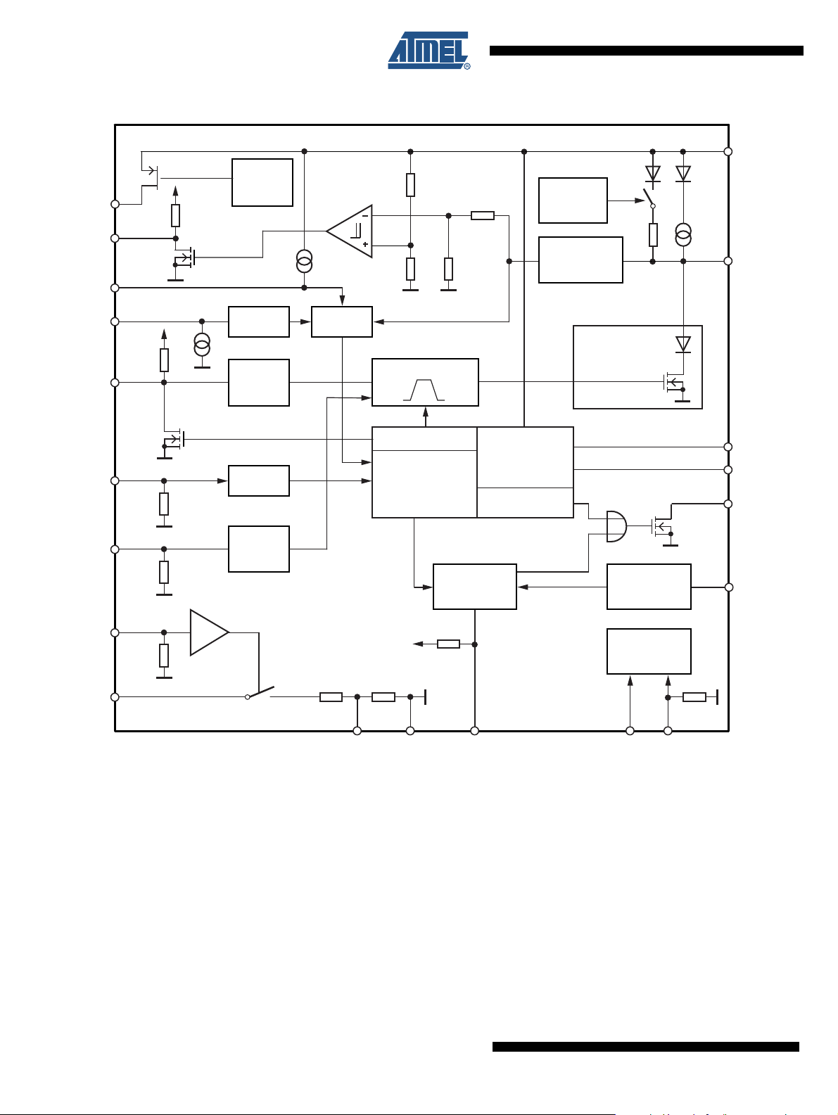
Figure 1-1. Block Diagram
High
Speed
Mode
Adjustable
Watchdog
Oscillator
Short Circuit and
Overtemperature
Protection
TXD
Time-out
Timer
Edge
Detection
Debounce
Time
Internal Testing
Unit
Control Unit
Slew Rate Control
Wake-up
Bus Timer
Mode Select
Undervoltage
Reset
Normal/Silent/
Fail-safe Mode
3.3V/50 mA/
±2%
5V/50 mA/
±2%
RF Filter
Watchdog
15
10
2
12
RXD
NTRIGGNDPV
PVCC
PVCC
PVCC
TMMODE
EN
TXD
SP_MODE
KL_15
17
WAKE
Receiver
7
4
59163
Normal and
Fail-safe
Mode
18
19
13
14
6
20
LIN
WD_OSC
NRES
PVCC
VCC
VS
8
DIV_ON
1
VBATT
5k
Normal and
Fail-safe
Mode
INH
11
2
ATA6628/ATA6630 [Preliminary]
9117C–AUTO–10/09
Page 3
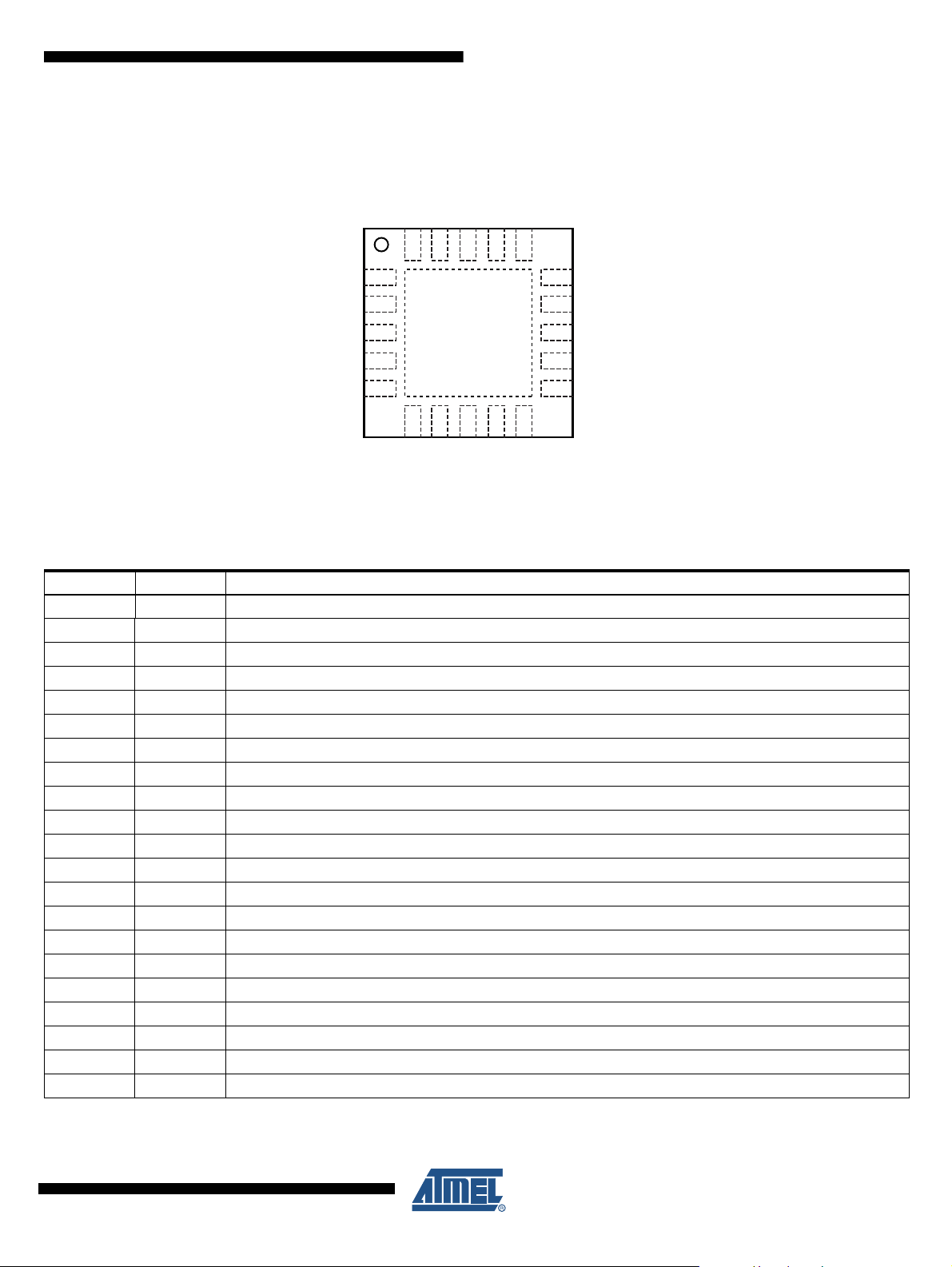
2. Pin Configuration
Figure 2-1. Pinning QFN20
ATA6628/ATA6630 [Preliminary]
MODE
KL15
PVCC
VCC
VS
VBATT
EN
NTRIG
WAKE
GND
20 19 18
1
2
3
4
5
67 8 109
LIN
ATA6628/30
QFN 5 mm 5 mm
0.65 mm pitch
20 lead
RXD
17
DIV_ON
PV
16
SP_MODE
15
14
13
12
11
TM
WD_OSC
NRES
TXD
INH
Table 2-1. Pin Description
Pin Symbol Function
1 VBATT Battery supply for the voltage divider
2 EN Enables the device into Normal Mode
3 NTRIG Low-level watchdog trigger input from microcontroller; if not needed, connect to PVCC
4 WAKE High-voltage input for local wake-up request; if not needed, connect to VS
5 GND System ground
6 LIN LIN-bus line input/output
7 RXD Receive data output
8 DIV_ON Input to switch on the internal voltage divider, active high
9 PV Voltage divider output
10 SP_MODE Input to switch the transceiver in High-speed Mode, active high
11 INH Battery related High-side switch
12 TXD Transmit data input; active low output (strong pull down) after a local wake up request
13 NRES Output undervoltage and watchdog reset (open drain)
14 WD_OSC External resistor for adjustable watchdog timing; if not needed, connect to GND
15 TM For factory testing only (tie to ground)
16 MODE For Debug Mode: Low watchdog is on; high watchdog is off
17 KL_15 Ignition detection (edge sensitive)
18 PVCC 3.3V/5V regulator sense input pin, connect to VCC
19 VCC 3.3V/5V regulator output/driver pin, connect to PVCC
20 VS Battery supply
Backside Heat slug is connected to GND
9117C–AUTO–10/09
3
Page 4

3. Functional Description
3.1 Physical Layer Compatibility
Since the LIN physical layer is independent from higher LIN layers (e.g., the LIN protocol layer),
all nodes with a LIN physical layer according to revision 2.x can be mixed with LIN physical layer
nodes, which, according to older versions (i.e., LIN 1.0, LIN 1.1, LIN 1.2, LIN 1.3), are without
any restrictions.
3.2 Supply Pin (VS)
The LIN operating voltage is VS = 5V to 27V. An undervoltage detection is implemented to disable data transmission if V
switching on VS, the IC starts in Fail-safe Mode, and the voltage regulator is switched on (i.e.,
3.3V/5V/50 mA output capability).
The supply current is typically 10 µA in Sleep Mode and 40 µA in Silent Mode.
3.3 Ground Pin (GND)
The IC is neutral on the LIN pin in the event of GND disconnection. It is able to handle a ground
shift up to 11.5% of VS. The mandatory system ground is pin 5.
3.4 Voltage Regulator Output Pin (VCC)
The internal 3.3V/5V voltage regulator is capable of driving loads up to 50 mA. It is able to supply the microcontroller and other ICs on the PCB and is protected against overloads by means of
current limitation and overtemperature shut-down. Furthermore, the output voltage is monitored
and will cause a reset signal at the NRES output pin if it drops below a defined threshold V
To boost up the maximum load current, an external NPN transistor may be used, with its base
connected to the VCC pin and its emitter connected to PVCC.
falls below VSth in order to avoid false bus messages. After
S
thun
.
3.5 Voltage Regulator Sense Pin (PVCC)
The PVCC is the sense input pin of the 3.3V/5V voltage regulator. For normal applications (i.e.,
when only using the internal output transistor), this pin must be connected to the VCC pin. If an
external boosting transistor is used, the PVCC pin must be connected to the output of this transistor, i.e., its emitter terminal.
3.6 Bus Pin (LIN)
A low-side driver with internal current limitation and thermal shutdown and an internal pull-up
resistor compliant with the LIN 2.x specification are implemented. The allowed voltage range is
between –27V and +40V. Reverse currents from the LIN bus to VS are suppressed, even in the
event of GND shifts or battery disconnection. LIN receiver thresholds are compatible with the
LIN protocol specification. The fall time from recessive to dominant bus state and the rise time
from dominant to recessive bus state are slope controlled.
4
ATA6628/ATA6630 [Preliminary]
9117C–AUTO–10/09
Page 5

3.7 Input/Output Pin (TXD)
In Normal Mode the TXD pin is the microcontroller interface used to control the state of the LIN
output. TXD must be pulled to ground in order to have a low LIN-bus. If TXD is high or not connected (internal pull-up resistor), the LIN output transistor is turned off, and the bus is in
recessive state. During Fail-safe Mode, this pin is used as output and is signalling the fail-safe
source. It is current-limited to < 8 mA.
3.8 TXD Dominant Time-out Function
The TXD input has an internal pull-up resistor. An internal timer prevents the bus line from being
driven permanently in dominant state. If TXD is forced to low for longer than t
LIN-bus driver is switched to recessive state. Nevertheless, when switching to Sleep Mode, the
actual level at the TXD pin is relevant.
To reactivate the LIN bus driver, switch TXD to high (> 10 µs).
3.9 Output Pin (RXD)
Tis output pin reports the state of the LIN-bus to the microcontroller. LIN high (recessive state) is
reported by a high level at RXD; LIN low (dominant state) is reported by a low level at RXD. The
output has an internal pull-up resistor with typically 5 kΩ to PVCC. The AC characteristics can be
defined with an external load capacitor of 20 pF.
ATA6628/ATA6630 [Preliminary]
>27ms, the
DOM
The output is short-circuit protected. RXD is switched off in Unpowered Mode (i.e., V
During Fail-safe Mode it is signalling the fail-safe source.
3.10 Enable Input Pin (EN)
The Enable Input pin controls the operation mode of the device. If EN is high, the circuit is in
Normal Mode, with transmission paths from TXD to LIN and from LIN to RXD both active. The
VCC voltage regulator operates with 3.3V/5V/50 mA output capability.
If EN is switched to low while TXD is still high, the device is forced to Silent Mode. No data transmission is then possible, and the current consumption is reduced to I
regulator has its full functionality.
If EN is switched to low while TXD is low, the device is forced to Sleep Mode. No data transmission is possible, and the voltage regulator is switched off.
3.11 Wake Input Pin (WAKE)
The WAKE Input pin is a high-voltage input used to wake up the device from Sleep Mode or
Silent Mode. It is usually connected to an external switch in the application to generate a local
wake-up. A pull-up current source, typically 10 µA, is implemented.
If a local wake-up is not needed for the application, connect the WAKE pin directly to the VS pin.
3.12 Mode Input Pin (MODE)
Connect the MODE pin directly or via an external resistor to GND for normal watchdog operation. To debug the software of the connected microcontroller, connect MODE pin to PVCC and
the watchdog is switched off.
= 0V).
S
typ. 40 µA. The VCC
VS
9117C–AUTO–10/09
Note: If you do not use the watchdog, connect pin MODE directly to PVCC.
5
Page 6

3.13 TM Input Pin
3.14 KL_15 Pin
3.15 INH Output Pin
The TM pin is used for final production measurements at Atmel®. In normal application, it has to
be always connected to GND.
The KL_15 pin is a high-voltage input used to wake up the device from Sleep or Silent Mode. It
is an edge-sensitive pin (low-to-high transition). It is usually connected to ignition to generate a
local wake-up in the application when the ignition is switched on. Although KL_15 pin is at high
voltage (V
directly to GND if you do not need it. A debounce timer with a typical Tdb
implemented.
The input voltage threshold can be adjusted by varying the external resistor due to the input current I
KL_15
capacitor of 100 nF are recommended. With this RC combination you can increase the wake-up
time Tw
You can also increase the wake-up time using external capacitors with higher values.
The INH Output pin is used to switch an external voltage regulator on during Normal and
Fail-safe Mode. The INH Output is a high-side switch, which is switched-off in Sleep and Silent
Mode. It is possible to switch off the external 1 kΩ master resistor via the INH pin for master
node applications.
), it is possible to switch the IC into Sleep or Silent Mode. Connect the KL_15 pin
Batt
of 160 µs is
Kl_15
. To protect this pin against voltage transients, a serial resistor of 47 kΩ and a ceramic
and, therefore, the sensitivity against transients on the ignition KL_15.
KL_15
3.16 Reset Output Pin (NRES)
The Reset Output pin, an open drain output, switches to low during VCC undervoltage or a
watchdog failure.
3.17 WD_OSC Output Pin
The WD_OSC Output pin provides a typical voltage of 1.2V, which supplies an external resistor
with values between 34 kΩ and 120 kΩ to adjust the watchdog oscillator time.
If the watchdog is disabled, this voltage is switched off and you can either tie to GND or leave
this pin open.
3.18 NTRIG Input Pin
The NTRIG Input pin is the trigger input for the window watchdog. A pull-up resistor is implemented. A negative edge triggers the watchdog. The trigger signal (low) must exceed a
minimum time t
to generate a watchdog trigger.
trigmin
3.19 Wake-up Events from Sleep or Silent Mode
•LIN-bus
• WAKE pin
•EN pin
• KL_15
6
ATA6628/ATA6630 [Preliminary]
9117C–AUTO–10/09
Page 7
3.20 DIV_ON Input Pin
The DIV_ON pin is a low voltage input. It is used to switch on or off the internal voltage divider
PV output directly with no time limitation (see Table 3-1 on page 7). It is switched on if DIV_ON
is high or it is switched off if DIV_ON is low. In Sleep Mode the DIV_ON functionality is disabled
and PV is off. An internal pull-down resistor is implemented.
3.21 VBATT Input Pin
The VBATT is a high voltage input pin to supply the internal voltage divider. In an application
with battery voltage monitoring, this pin is connected to V
10 nF capacitor to GND (see Figure 9-2 on page 31). The the divider ratio is 1:6.
3.22 PV Output Pin
For applications with battery monitoring, this pin is directly connected to the ADC of a microcontroller. For buffering the ADC input an external capacitor might be needed. This pin guarantees a
voltage and temperature stable output of a V
DIV_ON input pin.
Table 3-1. Table of Voltage Divider
ATA6628/ATA6630 [Preliminary]
via a 47Ω resistor in series and a
Battery
ratio. The PV output pin is controlled by the
Battery
Mode of Operation Input DiV_ON Voltage Divider Output PV
Fail-safe/Normal/
High-speed/Silent
Sleep
0Off
1On
0Off
1Off
3.23 SP_MODE Input Pin
The SP_MODE pin is a low-voltage input. High-speed Mode of the transceiver can be activated
via a high level during Normal Mode. Return to LIN 2.x Transceiver Mode with slope control is
possible if you switch the SP_MODE pin to low.
9117C–AUTO–10/09
7
Page 8
4. Modes of Operation
Unpowered Mode
(See Section 4.5)
a: V
S
> VS
thF
b: VS < VS
thU
c: Bus wake-up event
d: Wake up from WAKE or KL_15 pin
Fail-safe Mode
VCC: 3.3V/5V/50 mA
with undervoltage monitoring
Communication: OFF
Watchdog: ON
Silent Mode
VCC: 3.3V/5V/50 mA
with undervoltage monitoring
Communication: OFF
Watchdog: OFF
Sleep Mode
VCC: switched off
Communication: OFF
Watchdog: OFF
Go to silent command
a
TXD = 0
EN = 0
TXD = 1
EN = 0
EN = 1
EN = 1
EN = 1
b
b
b
c + d + e
e
c + d
b
Normal Mode
VCC: 3.3V/5V/50 mA
with undervoltage detection
watchdog: ON
High level at
pin SP_MODE:
High-speed Mode
Transceiver ≤ 115 kBaud
LIN 2.1
Transceiver
≤ 20 kBaud
TXD time-out
timer on
Go to sleep command
e: NRES switches to low
Go to normal command
Figure 4-1. Modes of Operation
Table 4-1. Table of Modes
Mode of
Operation Transceiver Pin LIN V
Unpowered Off Recessive On GND On On Off
Fail-safe Off Recessive 3.3V/5V GND On 1.23V On
Normal/
High-speed
Silent Off Recessive 3.3V/5V GND Off 0V Off
Sleep Off Recessive 0V GND Off 0V Off
8
ATA6628/ATA6630 [Preliminary]
CC
Pin Mode Watchdog Pin WD_OSC Pin INH
On TXD depending 3.3V/5V GND On 1.23V On
9117C–AUTO–10/09
Page 9
4.1 Normal Mode
4.2 Silent Mode
ATA6628/ATA6630 [Preliminary]
This is the normal transmitting and receiving mode. The voltage regulator is active and can
source up to 50 mA. The undervoltage detection is activated. The watchdog needs a trigger signal from NTRIG to avoid resets at NRES. If NRES is switched to low, the IC changes its state to
Fail-safe Mode.
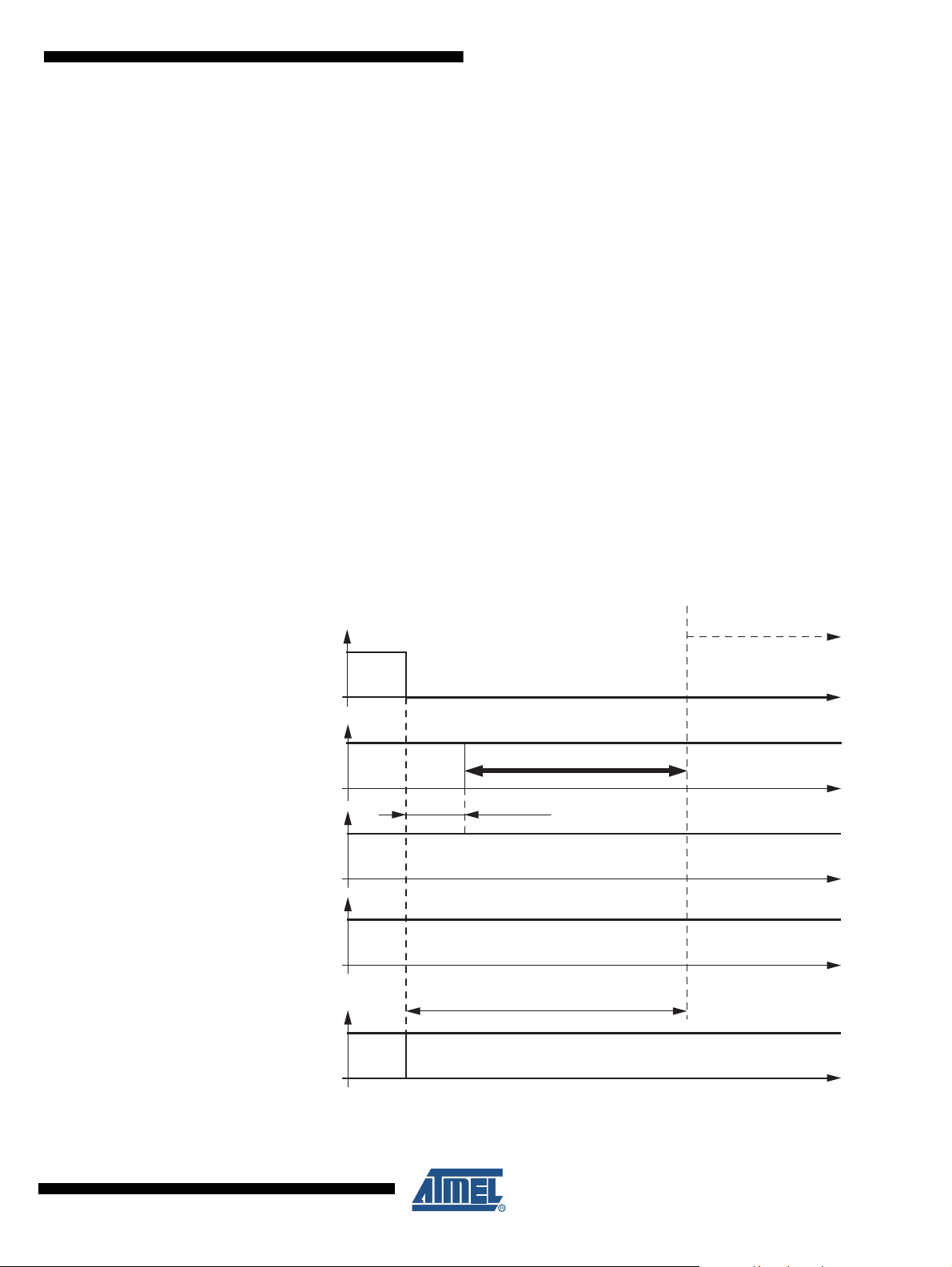
A falling edge at EN when TXD is high switches the IC into Silent Mode. The TXD Signal has to
be logic high during the Mode Select window (see Figure 4-2 on page 9). The transmission path
is disabled in Silent Mode. The INH output is switched off and the voltage divider is enabled. The
overall supply current from V
put current I
VCC
.
The 3.3V/5V regulator with 2% tolerance can source up to 50 mA. The internal slave termination
between the LIN pin and the VS pin is disabled in Silent Mode to minimize the current consumption in the event that the LIN pin is short-circuited to GND. Only a weak pull-up current (typically
10 µA) between the LIN pin and the VS pin is present. Silent Mode can be activated independently from the actual level on the LIN, WAKE, or KL_15 pins. If an undervoltage condition
occurs, NRES is switched to low, and the IC changes its state to Fail-safe Mode.
is a combination of the I
Batt
= 40 µA plus the VCC regulator out-
VSsi
A voltage less than the LIN Pre_Wake detection VLINL at the LIN pin activates the internal LIN
receiver and starts the wake-up detection timer.
Figure 4-2. Switch to Silent Mode
Normal Mode
EN
TXD
NRES
VCC
LIN
Mode select window
t
= 3.2 µs
d
Delay time silent mode
t
_silent = maximum 20 µs
d
Silent Mode
9117C–AUTO–10/09
LIN switches directly to recessive mode
9
Page 10
A falling edge at the LIN pin followed by a dominant bus level maintained for a certain time
period (t
) and the following rising edge at the LIN pin (see Figure 4-3 on page 10) result in a
bus
remote wake-up request. The device switches from Silent Mode to Fail-safe Mode. The internal
LIN slave termination resistor is switched on. The remote wake-up request is indicated by a low
level at the RXD pin to interrupt the microcontroller (see Figure 4-3 on page 10). EN high can be
used to switch directly to Normal Mode.
Figure 4-3. LIN Wake-up from Silent Mode
LIN bus
RXD
TXD
Watchdog
VCC
voltage
regulator
Bus wake-up filtering time
Node in silent mode
Silent mode 3.3V/5V/50 mA Fail safe mode 3.3V/5V/50 mA
t
bus
Watchdog off Start watchdog lead time t
Fail-safe mode Normal mode
Don't care
Low
HighHigh
d
Normal mode
10
EN
NRES
Undervoltage detection active
ATA6628/ATA6630 [Preliminary]
EN High
9117C–AUTO–10/09
Page 11
4.3 Sleep Mode
Delay time sleep mode
t
d_sleep
= maximum 20 µs
LIN switches directly to recessive mode
t
d
= 3.2 µs
LIN
VCC
NRES
TXD
EN
Sleep Mode
Normal Mode
Mode select window
ATA6628/ATA6630 [Preliminary]
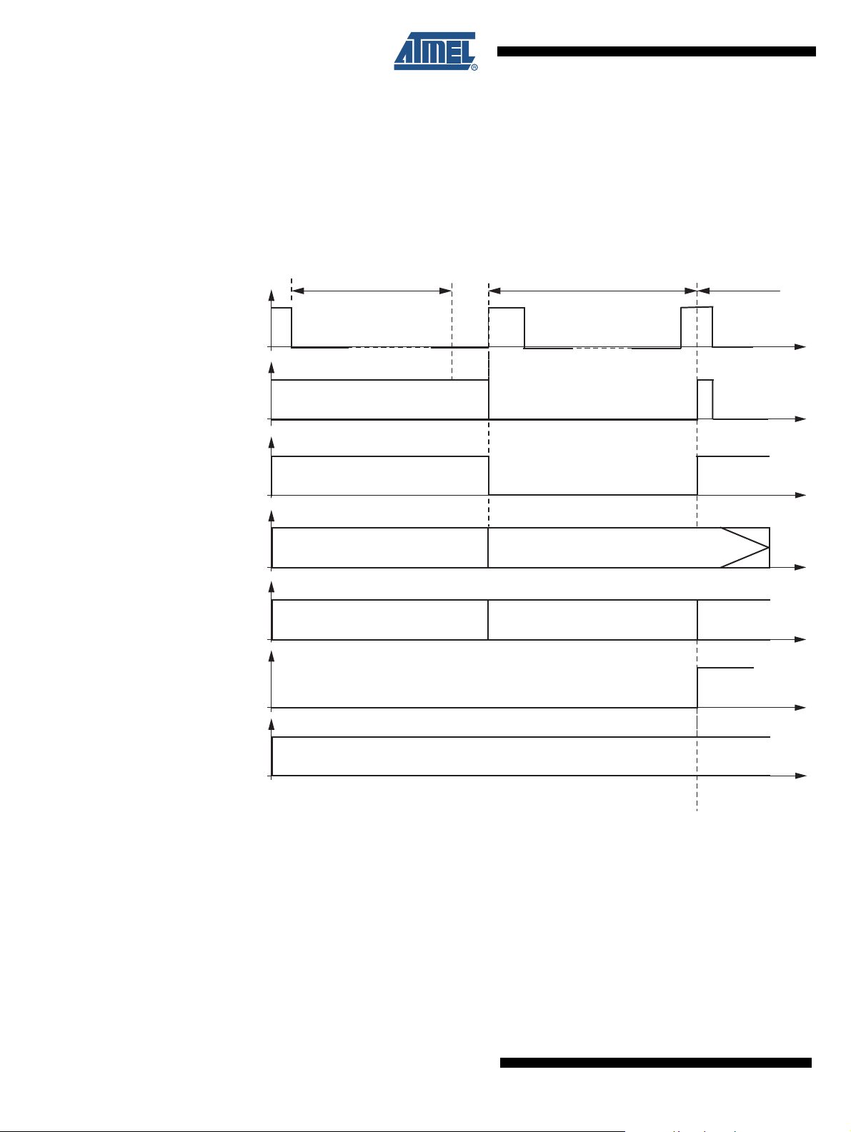
A falling edge at EN when TXD is low switches the IC into Sleep Mode. The TXD Signal has to
be logic low during the Mode Select window (Figure 4-4 on page 11). In order to avoid any influence to the LIN-pin during switching into sleep mode it is possible to switch the EN up to 3.2 µs
earlier to Low than the TXD. Therefore, the best an easiest way are two falling edges at TXD
and EN at the same time. The transmission path is disabled in Sleep Mode. The supply current
I
from V
VSsleep
The INH output, the PV output and the VCC regulator are switched off. NRES and RXD are low.
The internal slave termination between the LIN pin and VS pin is disabled to minimize the current consumption in the event that the LIN pin is short-circuited to GND. Only a weak pull-up
current (typically 10 µA) between the LIN pin and the VS pin is present. Sleep Mode can be activated independently from the current level on the LIN, WAKE, or KL_15 pin.
A voltage less than the LIN Pre_Wake detection VLINL at the LIN pin activates the internal LIN
receiver and starts the wake-up detection timer.
Figure 4-4. Switch to Sleep Mode
is typically 10 µA.
Batt
9117C–AUTO–10/09
11
Page 12

A falling edge at the LIN pin followed by a dominant bus level maintained for a certain time
period (t
) and a rising edge at pin LIN result in a remote wake-up request. The device
bus
switches from Sleep Mode to Fail-safe Mode.
The VCC regulator is activated, and the internal LIN slave termination resistor is switched on.
The remote wake-up request is indicated by a low level at the RXD pin to interrupt the microcontroller (see Figure 4-5 on page 12).
EN high can be used to switch directly from Sleep/Silent to Fail-safe Mode. If EN is still high after
VCC ramp up and undervoltage reset time, the IC switches to the Normal Mode.
Figure 4-5. LIN Wake Up from Sleep Mode
Bus wake-up filtering time
LIN bus
t
bus
Fail-safe Mode Normal Mode
RXD
TXD
VCC
voltage
regulator
EN
NRES
Watchdog
Low or floating
Off state
Regulator wake-up time
Reset
time
Floating
Watchdog off Start watchdog lead time td
Low
On state
Microcontroller
start-up time delay
EN High
12
ATA6628/ATA6630 [Preliminary]
9117C–AUTO–10/09
Page 13

ATA6628/ATA6630 [Preliminary]
I
VSsleep/silent
I
VSsleep
I
VSfail
+ I
LINwake
I
VSsleep
V
BUSdom
V
LINL
I
VS
t
mon
LIN Pre-wake
LIN dominant state
LIN BUS
Mode of
operation
Int. Pull-up
Resistor
RLIN
Wake-up Detection Phase
off (disabled)
Sleep/Silent Mode Sleep/Silent Mode
4.4 Sleep or Silent Mode: Behavior at a Floating LIN-bus or a Short Circuited LIN to GND
In Sleep or in Silent Mode the device has a very low current consumption even during shortcircuits or floating conditions on the bus. A floating bus can arise if the Master pull-up resistor is
missing, e.g., if it is switched off when the LIN- Master is in sleep mode or even if the power
supply of the Master node is switched off.
In order to minimize the current consumption I
in sleep or silent mode during voltage levels at
VS
the LIN-pin below the LIN pre-wake threshold, the receiver is activated only for a specific time
tmon. If t
elapses while the voltage at the bus is lower than Pre-wake detection low (V
mon
LINL
and higher than the LIN dominant level, the receiver is switched off again and the circuit
changes back to sleep respectively Silent Mode. The current consumption is then the result of
I
or I
VSsleep
Even if the voltage rises above the Pre-wake detection high (V
VSsilent
plus I
. If a dominant state is reached on the bus no wake-up will occur.
LINwake
), the IC will stay in sleep
LINH
respectively silent mode (see Figure 4-6).
This means the LIN-bus must be above the Pre-wake detection threshold V
for a few micro-
LINH
seconds before a new LIN wake-up is possible.
Figure 4-6. Floating LIN-bus During Sleep or Silent Mode
)
9117C–AUTO–10/09
If the ATA6628/ATA6630 is in Sleep or Silent Mode and the voltage level at the LIN-bus is in
dominant state (V
example), the IC switches back to Sleep Mode respectively Silent Mode. The V
consumption then consists of I
IC switches directly to Fail-safe Mode (see Figure 4-7 on page 14).
LIN
< V
) for a time period exceeding t
BUSdom
or I
VSsleep
VSsilent
plus I
LINWAKE
(during a short circuit at LIN, for
mon
current
S
. After a positive edge at pin LIN the
13
Page 14

Figure 4-7. Short Circuit to GND on the LIN bus During Sleep- or Silent Mode
Sleep/Silent
Mode
I
VSsleep/silent
I
VSfail
+ I
LINwake
I
VSsleep/silent
V
BUSdom
V
LINL
LIN Pre-wake
LIN dominant state
LIN BUS
I
VS
Mode of
operation
Int. Pull-up
Resistor
RLIN
off (disabled) on (enabled)
Wake-up Detection PhaseSleep/Silent Mode Fail-Safe Mode
t
mon
t
mon
14
ATA6628/ATA6630 [Preliminary]
9117C–AUTO–10/09
Page 15

4.5 Fail-safe Mode
ATA6628/ATA6630 [Preliminary]
The device automatically switches to Fail-safe Mode at system power-up. The voltage regulator
is switched on (V
switches to low for t
switched off. The IC stays in this mode until EN is switched to high. The IC then changes to Normal Mode. A power down of V
Fail-safe Mode after power up. A low at NRES switches into Fail-safe Mode directly. During
Fail-safe Mode, the TXD pin is an output and signals the fail-safe source. The watchdog is
switched on.
The LIN SBC can operate in different Modes, like Normal, Silent, or Sleep Mode. The functionality of these modes is described in Table 4-2.
Table 4-2. TXD, RXD Depending from Operation Modes
Different Modes TXD RXD
Fail-safe Mode Signalling fail-safe sources (see Table 4-3 and Table 4-4)
Normal Mode Follows data transmission
Silent Mode High High
= 3.3V/5V/2%/50 mA) (see Figure 5-1 on page 19). The NRES output
CC
= 4 ms and gives a reset to the microcontroller. LIN communication is
res
(VS<VS
Batt
) during Silent or Sleep Mode switches the IC into
thU
A wake-up event from either Silent or Sleep Mode will be signalled to the microcontroller using
the two pins RXD and TXD. The coding is shown in Table 4-3.
A wake-up event will lead the IC to the Fail-safe Mode.
Table 4-3. Signalling Fail-safe Sources
Fail-safe Sources TXD RXD
LIN wake-up (pin LIN) Low Low
Local wake-up (at pin Wake, pin KL15) Low High
(battery) undervoltage detection High Low
VS
th
Table 4-4. Signalling in Fail-safe Mode after Reset (NRES was Low), Shows the Reset
Source at TXD and RXD Pins
Fail-safe Sources TXD RXD
VCC undervoltage at NRES High Low
Watchdog reset at NRES High High
9117C–AUTO–10/09
15
Page 16

4.6 Unpowered Mode
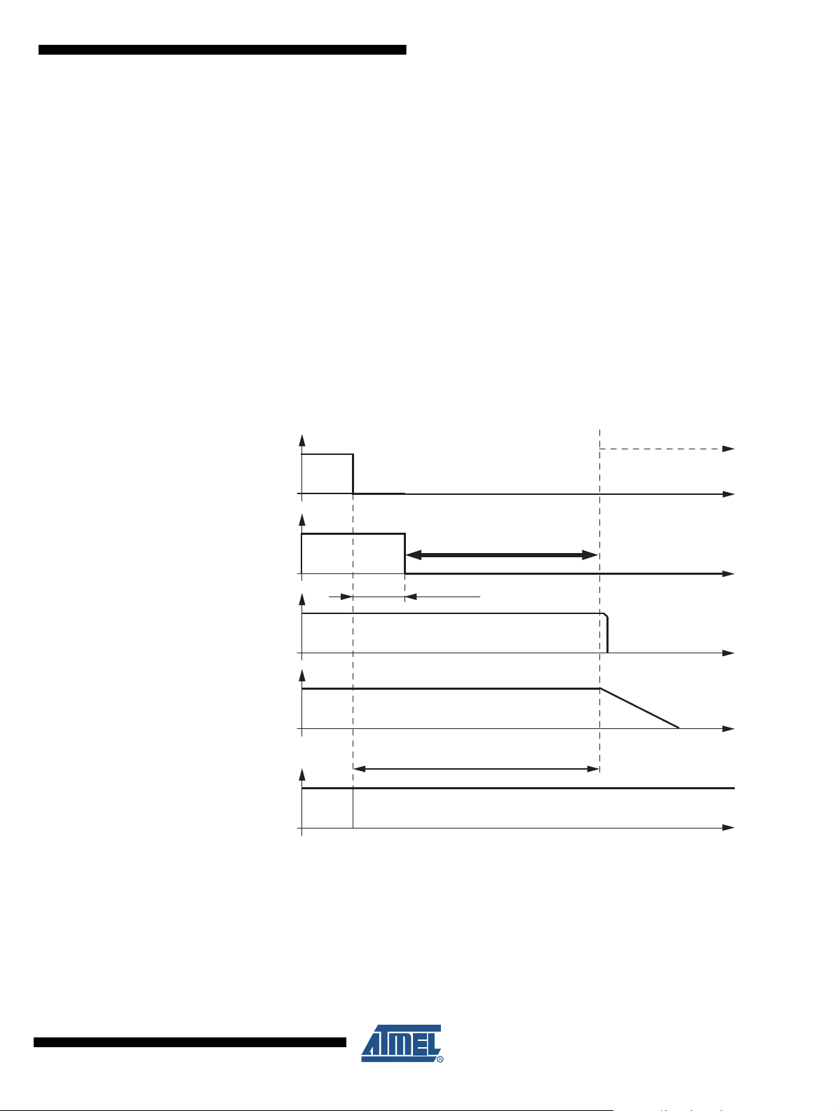
If you connect battery voltage to the application circuit, the voltage at the VS pin increases
according to the block capacitor (see Figure 5-1 on page 19). After VS is higher than the VS
undervoltage threshold VS
The VCC output voltage reaches its nominal value after t
VCC capacitor and the load.
, the IC mode changes from Unpowered Mode to Fail-safe Mode.
th
. This time, t
VCC
, depends on the
VCC
The NRES is low for the reset time delay t
. During this time, t
reset
possible.
IF VS drops below VS
, then the IC switches to Unpowered Mode. The behavior of VCC, NRES
th
and LIN is shown in Figure 4-8. The watchdog needs to be triggered.
Figure 4-8. VCC versus VS for the VCC = 3.3V Regulator
6.0
5.5
5.0
4.5
4.0
3.5
3.0
V in V
2.5
2.0
1.5
1.0
0.5
0.0
0.0 0 .5 1.0 1.5 2.0 2.5 3 .0 3 .5 4.0 4 .5 5.0 5.5 6.0
Regulator drop voltage V
VS
D
NRES
VCC
VS in V
, no mode change is
reset
LIN
4.7 High-speed Mode
If SP_MODE pin is high and the IC is in Normal Mode, the slew rate control is switched off. The
slope time of the LIN falling edge is t
depends on the LIN capacitive and resistive load. To achieve a high baud rate it is recommended to use a small resistor (500Ω) and a low capacitor. This allows very fast data
transmission up to 115 kBaud, e.g., for electronic control (ECU) tests and microcontroller program or data download. In this mode superior EMC performance is not guaranteed.
16
ATA6628/ATA6630 [Preliminary]
< 2 µs. The slope time of the LIN rising edge strongly
S_Fall
9117C–AUTO–10/09
Page 17

ATA6628/ATA6630 [Preliminary]
5. Wake-up Scenarios from Silent or Sleep Mode
5.1 Remote Wake-up via Dominant Bus State
A voltage less than the LIN Pre_Wake detection V
receiver and starts the wake-up detection timer.
at the LIN pin activates the internal LIN
LINL
A falling edge at the LIN pin followed by a dominant bus level V
time period (t
switches from Silent or Sleep Mode to Fail-safe Mode. The VCC voltage regulator is/remains
activated, the INH pin is switched to high, and the internal slave termination resistor is switched
on. The remote wake-up request is indicated by a low level at the RXD pin to generate an interrupt for the microcontroller and a strong pull down at TXD.
) and a rising edge at pin LIN result in a remote wake-up request. The device
BUS
5.2 Local Wake-up via Pin WAKE
A falling edge at the WAKE pin followed by a low level maintained for a certain time period
(t
) results in a local wake-up request. The device switches to Fail-safe Mode. The internal
WAKE
slave termination resistor is switched on. The local wake-up request is indicated by a low level at
the TXD pin to generate an interrupt for the microcontroller. When the Wake pin is low, it is possible to switch to Silent or Sleep Mode via pin EN. In this case, the wake-up signal has to be
switched to high > 10 µs before the negative edge at WAKE starts a new local wake-up request.
5.3 Local Wake-up via Pin KL_15
A positive edge at pin KL_15 followed by a high voltage level for a certain time period (> t
results in a local wake-up request. The device switches into the Fail-safe Mode. The internal
slave termination resistor is switched on. The extra long wake-up time ensures that no transients
at KL_15 create a wake-up. The local wake-up request is indicated by a low level at the TXD pin
to generate an interrupt for the microcontroller. During high-level voltage at pin KL_15, it is possible to switch to Silent or Sleep Mode via pin EN. In this case, the wake-up signal has to be
switched to low > 250 µs before the positive edge at KL_15 starts a new local wake-up request.
With external RC combination, the time is even longer.
maintained for a certain
BUSdom
KL_15
)
5.4 Wake-up Source Recognition
The device can distinguish between different wake-up sources (see Table 4-4 on page 15).
The wake-up source can be read on the TXD and RXD pin in Fail-safe Mode. These flags are
immediately reset if the microcontroller sets the EN pin to high (see Figure 4-3 on page 10 and
Figure 4-5 on page 12) and the IC is in Normal mode.
9117C–AUTO–10/09
17
Page 18

5.5 Fail-safe Features
• During a short-circuit at LIN to V
• During a short-circuit from LIN to GND the IC can be switched into Sleep or Silent Mode and
• Sleep or Silent Mode: During a floating condition on the bus the IC switches back to Sleep
• The reverse current is < 2 µA at the LIN pin during loss of V
• During a short circuit at VCC, the output limits the output current to I
• EN pin provides a pull-down resistor to force the transceiver into recessive mode if EN is
• RXD pin is set floating if V
• TXD pin provides a pull-up resistor to force the transceiver into recessive mode if TXD is
• If TXD is short-circuited to GND, it is possible to switch to Sleep Mode via ENABLE
• If the WD_OSC pin has a short-circuit to GND or the resistor is disconnected, the watchdog
• If there is no NTRIG signal and short circuit at WD_OSC the NRES switches to low after typ.
, the output limits the output current to I
Battery
the power dissipation, the chip temperature exceeds T
off. The chip cools down and after a hysteresis of T
hys
, and the LIN output is switched
LINoff
, switches the output on again. RXD
BUS_lim
. Due to
stays on high because LIN is high. During LIN overtemperature switch-off, the VCC regulator
works independently.
even in this case the current consumption is lower than 45 µA in Sleep Mode and lower than
80 µA in Silent Mode. If the short-circuit disappears, the IC starts with a remote wake-up.
Mode/Silent Mode automatically and thereby the current consumption is lower than
45 µA/80 µA.
. This is optimal behavior for
Batt
bus systems where some slave nodes are supplied from battery or ignition.
. Because of
VCClim
undervoltage, NRES switches to low and sends a reset to the microcontroller if NRES is
connected to the microcontroller. The IC switches into Fail-safe Mode. If the chip temperature
exceeds the value T
hysteresis of T
, switches the output on again. Because of the Fail-safe Mode, the VCC
hys
, the VCC output switches off. The chip cools down and after a
VCCoff
voltage will switch on again although EN is switched off from the microcontroller. The
microcontroller can start with its normal operation.
disconnected.
is disconnected.
Batt
disconnected.
runs with an internal oscillator and guarantees a reset.
90 ms. For an open circuit (no resistor) at WD_OSC it switches to low after typ. 390 ms.
18
ATA6628/ATA6630 [Preliminary]
9117C–AUTO–10/09
Page 19

5.6 Voltage Regulator
0
10
20
3 0
40
50
60
3 5791113 15 17 19
VS/V
I
VCC
/mA
T
amb
= 125°C
T
amb
= 105°C
The voltage regulator needs an external capacitor for compensation and for smoothing the disturbances from the microcontroller. It is recommended to use an electrolythic capacitor with
C > 1.8 µF and a ceramic capacitor with C = 100 nF. The values of these capacitors can be varied by the customer, depending on the application.
ATA6628/ATA6630 [Preliminary]
The main power dissipation of the IC is created from the VCC output current I
, which is
VCC
needed for the application. In Figure 5-2 on page 19 the safe operating area of the
ATA6628/ATA6630 is shown.
Figure 5-1. VCC Voltage Regulator: Ramp-up and Undervoltage Detection
VS
12V
5.5V/3.8V
t
VCC
5V/3.3V
V
thun
res_f
t
NRES
5V/3.3V
T
VCC
T
Reset
T
Figure 5-2. Power Dissipation: Safe Operating Area versus VCC Output Current and Supply
9117C–AUTO–10/09
For microcontroller programming, it may be necessary to supply the VCC output via an external
power supply while the V
problem for the system basis chip.
Voltage V
t
at Different Ambient Temperatures Due to R
S
Pin of the system basis chip is disconnected. This behavior is no
S
= 35 K/W
thja
19
Page 20

6. Watchdog
The watchdog anticipates a trigger signal from the microcontroller at the NTRIG (negative edge)
input within a time window of T
t
> 200 ns. If a triggering signal is not received, a reset signal will be generated at output
trigmin
. The trigger signal must exceed a minimum time
wd
NRES. The timing basis of the watchdog is provided by the internal oscillator. Its time period,
T
, is adjustable via the external resistor R
osc
(34 kΩ to 120 kΩ).
wd_osc
During Silent or Sleep Mode the watchdog is switched off to reduce current consumption.
The minimum time for the first watchdog pulse is required after the undervoltage reset at NRES
disappears. It is defined as lead time t
t
starts with the negative edge of the RXD output.
d
. After wake up from Sleep or Silent Mode, the lead time
d
6.1 Typical Timing Sequence with R
The trigger signal Twd is adjustable between 20 ms and 64 ms using the external resistor
R
WD_OSC
For example, with an external resistor of R
watchdog are as follows:
t
osc
t
OSC
t
= 7895 × 19.6 µs = 155 ms
d
t
= 1053 × 19.6 µs = 20.6 ms
1
t
= 1105 × 19.6 µs = 21.6 ms
2
t
nres
After ramping up the battery voltage, the 5V regulator is switched on. The reset output NRES
stays low for the time t
the trigger sequence from the microcontroller. The lead time, t
t
d
ger pulse NTRIG occurs during this time, the time t
occurs during the time t
t
d
troller is anticipated within the time frame of t
the trigger pulse must be longer than t
dog sequence. If the triggering signal fails in this open window t
to ground. A triggering signal during the closed window t
.
= 0.405 × R
WD_OSC
= 19.6 µs due to 51 kΩ
= constant = 4 ms
= 155 ms. In this time, the first watchdog pulse from the microcontroller is required. If the trig-
= 155 ms. The times t1 and t2 have a fixed relationship. A triggering signal from the microcon-
WD_OSC
– 0.0004 × (R
reset
d
= 51 kΩ
WD_OSC
WD_OSC
(typically 4 ms), then it switches to high, and the watchdog waits for
, a watchdog reset with t
TRIG,min
= 51 kΩ ±1%, the typical parameters of the
)2 (R
WD_OSC
= 21.6 ms. To avoid false triggering from glitches,
2
in kΩ ; t
starts immediately. If no trigger signal
1
= 4 ms will reset the microcontroller after
NRES
in µs)
osc
, follows the reset and is
d
> 200 ns. This slope serves to restart the watch-
, the NRES output will be drawn
2
immediately switches NRES to low.
1
20
ATA6628/ATA6630 [Preliminary]
9117C–AUTO–10/09
Page 21

ATA6628/ATA6630 [Preliminary]
Figure 6-1. Timing Sequence with R
VCC
3.3V
5V
NRES
NTRIG
Undervoltage Reset Watchdog Reset
= 4 ms
t
reset
6.2 Worst Case Calculation with R
The internal oscillator has a tolerance of 20%. This means that t1 and t2 can also vary by 20%.
The worst case calculation for the watchdog period t
The ideal watchdog time t
t
.
2
t
= 0.8 × t1 = 16.5 ms, t
1,min
t
= 0.8 × t2 = 17.3 ms, t
2,min
t
= t
wdmax
t
= t
wdmin
t
= 29.3 ms ±4.5 ms (±15%)
wd
A microcontroller with an oscillator tolerance of ±15% is sufficient to supply the trigger inputs
correctly.
+ t
1min
= 24.8 ms
1max
2min
= 51 kΩ
t
= 20.6 ms t2 = 21 ms
1
WD_OSC
wd
1,max
WD_OSC
td = 155 ms
> 200 ns
t
trig
= 51 kΩ
is between the maximum t1 and the minimum t1 plus the minimum
= 1.2 × t1 = 24.8 ms
= 1.2 × t2 = 26 ms
2,max
= 16.5 ms + 17.3 ms = 33.8 ms
t
1
t
wd
is calculated as follows.
wd
t
= 4 ms
nres
t
2
9117C–AUTO–10/09
Table 6-1. Typical Watchdog Timings
Oscillator
R
WD_OSC
kΩ
Period
t
/µs
osc
34 13.3 105 14.0 14.7 19.9 4
51 19.61 154.8 20.64 21.67 29.32 4
91 33.54 264.80 35.32 37.06 50.14 4
120 42.84 338.22 45.11 47.34 64.05 4
Lead
Time
td/ms
Closed
Window
t1/ms
Open Window
t2/ms
Trigger Period from
Microcontroller
twd/ms
Reset Time
t
/ms
nres
21
Page 22

7. Absolute Maximum Ratings
Stresses beyond those listed under “Absolute Maximum Ratings” may cause permanent damage to the device. This is a stress rating
only and functional operation of the device at these or any other conditions beyond those indicated in the operational sections of this
specification is not implied. Exposure to absolute maximum rating conditions for extended periods may affect device reliability.
Parameters Symbol Min. Typ. Max. Unit
Supply voltage V
S
V
S
Pulse time ≤ 500 ms
= 25°C
T
a
Output current I
VCC
≤ 50 mA
V
S
Pulse time ≤ 2min
T
= 25°C
a
Output current I
VCC
≤ 50 mA
V
S
WAKE (with 2.7 kΩ serial resistor)
KL_15 (with 47 kΩ/100 nF)
VBATT (with 47Ω/10 nF)
DC voltage
Transient voltage due to ISO7637
(coupling 1 nF)
INH
- DC voltage –0.3 V
LIN, VBATT
- DC voltage –27 +40 V
Logic pins (RxD, TxD, EN, NRES, NTRIG,
WD_OSC, MODE, TM, DIV_ON,
SP_MODE, PV)
Output current NRES I
NRES
PVCC DC voltage
VCC DC voltage
ESD according to IBEE LIN EMC
Test Spec. 1.0 following IEC 61000-4-2
- Pin VS, LIN to GND
- Pin WAKE (2.7 kΩ, 10 nF) to GND
- Pin VBATT (10 nF) to GND
HBM ESD
ANSI/ESD-STM5.1
JESD22-A114
AEC-Q100 (002)
MIL-STD-883 (M3015.7)
CDM ESD STM 5.3.1 ±750 V
MM ESD
EIA/JESD22-A115
ESD STM5.2
AEC-Q100 (002)
ESD HBM following STM5.1 with 1.5 kΩ
100 pF
- Pin VS, LIN, WAKE to GND
Junction temperature T
Storage temperature T
j
s
–0.3 +40 V
+40 V
27 V
–1
–150
+40
+100
+ 0.3 V
S
–0.3 VCC + 0.5V V
+2 mA
–0.3
–0.3
+5.5
+6.5
±6 KV
±3 KV
±200 V
±8 KV
–40 +150 °C
–55 +150 °C
V
V
V
V
22
ATA6628/ATA6630 [Preliminary]
9117C–AUTO–10/09
Page 23

ATA6628/ATA6630 [Preliminary]
8. Thermal Characteristics
Parameters Symbol Min. Typ. Max. Unit
Thermal resistance junction to heat slug R
thjc
Thermal resistance junction to ambient,
where heat slug is soldered to PCB
R
thja
35 K/W
according to Jedec
Thermal shutdown of VCC regulator 150 165 170 °C
Thermal shutdown of LIN output 150 165 170 °C
Thermal shutdown hysteresis 10 °C
9. Electrical Characteristics
5V < VS < 27V, –40°C < Tj < 150°C, unless otherwise specified. All values refer to GND pins
No. Parameters Test Conditions Pin Symbol Min. Typ. Max. Unit Type*
1 VS Pin
1.1 Nominal DC voltage range VS V
S
Sleep Mode
> VS – 0.5V
V
LIN
VS I
VSsleep
VS < 14V (Tj = 25°C)
Supply current in Sleep
1.2
Mode
Sleep Mode
V
> VS – 0.5V
LIN
VS < 14V (Tj = 125°C)
Sleep Mode, V
LIN
= 0V
Bus shorted to GND
< 14V
V
S
VS I
VS I
VSsleep_short
VSsleep
Bus recessive
VS < 14V (Tj = 25°C)
VS I
VSsi
Without load at VCC
Bus recessive
Supply current in Silent
1.3
Mode
< 14V (Tj = 125°C)
V
S
Without load at VCC
VS I
VSsi
Silent Mode
V
< 14V
S
Bus shorted to GND
VS I
VSsi_short
Without load at VCC
Supply current in Normal
1.4
Mode
Supply current in Normal
1.5
Mode
Supply current in Fail-safe
1.6
Mode
1.7 VS undervoltage threshold
VS undervoltage threshold
1.8
hysteresis
Bus recessive
V
S
< 14V
VS I
Without load at VCC
Bus recessive
VS < 14V
load current 50 mA
V
CC
VS I
Bus recessive, RXD is low
VS < 14V
VS I
Without load at VCC
Switch to Unpowered Mode VS V
Switch to Fail-safe Mode VS V
VS V
VSrec
VSdom
VSfail
SthU
SthF
Sth_hys
*) Type means: A = 100% tested, B = 100% correlation tested, C = Characterized on samples, D = Design parameter
527VA
31014µAA
51116µAA
TBD TBD 45 µA A
30 40 50 µA A
30 40 50 µA A
TBD TBD 80 µA A
0.3 0.8 mA A
50 53 mA A
0.8 1.5 mA A
44.24.4VA
4.3 4.5 4.9 V A
10 K/W
0.3 V A
9117C–AUTO–10/09
23
Page 24

9. Electrical Characteristics (Continued)
5V < VS < 27V, –40°C < Tj < 150°C, unless otherwise specified. All values refer to GND pins
No. Parameters Test Conditions Pin Symbol Min. Typ. Max. Unit Type*
2 RXD Output Pin
Low-level output sink
2.1
current
2.2 Low-level output voltage I
2.3 Internal resistor to PVCC RXD R
3 TXD Input/Output Pin
3.1 Low-level voltage input TXD V
3.2 High-level voltage input TXD V
3.3 Pull-up resistor V
3.4 High-level leakage current V
Low-level output sink
3.5
current
4 EN Input Pin
4.1 Low-level voltage input EN V
4.2 High-level voltage input EN V
4.3 Pull-down resistor V
4.4 Low-level input current V
5 NTRIG Watchdog Input Pin
5.1 Low-level voltage input NTRIG V
5.2 High-level voltage input NTRIG V
5.3 Pull-up resistor V
5.4 High-level leakage current V
6Mode Input Pin
6.1 Low-level voltage input MODE V
6.2 High-level voltage input MODE V
6.3 High-level leakage current
7 INH Output Pin
7.1 High-level voltage I
Switch-on resistance
7.2
between VS and INH
7.3 Leakage current
8 LIN Bus Driver
Driver recessive output
8.1
voltage
8.2 Driver dominant voltage
*) Type means: A = 100% tested, B = 100% correlation tested, C = Characterized on samples, D = Design parameter
Normal Mode
V
=0V
LIN
=0.4V
V
RXD
= 1 mA RXD V
RXD
=0V TXD R
TXD
TXD=VCC
RXD I
TXD I
Fail-safe Mode, wake up
V
= V
LIN
V
V
V
V
S
= 0V
WAKE
= 0.4V
TXD
= V
EN
CC
= 0V EN I
EN
= 0V NTRIG R
NTRIG
= V
NTRIG
MODE
MODE
INH
CC
= VCC or
= 0V
= –15 mA INH V
TXD I
EN R
NTRIG I
MODE I
INH R
Sleep Mode
V
= 0V/27V, VS = 27V
INH
INH I
Load1/Load2 LIN V
= 7V
V
R
VS
load
= 500 Ω
LIN V
RXD
RXDL
RXD
TXDL
TXDH
TXD
TXD
TXDwake
ENL
ENH
EN
EN
NTRIGL
NTRIGH
NTRIG
NTRIG
MODEL
MODEH
MODE
INHH
INH
INHL
BUSrec
_LoSUP
1.3 2.5 8 mA A
0.4 V A
357kΩ A
–0.3 +0.8 V A
+
V
2
CC
0.3V
VA
125 250 400 kΩ A
–3 +3 µA A
22.58mAA
–0.3 +0.8 V A
V
+
2
CC
0.3V
VA
50 125 200 kΩ A
–3 +3 µA A
–0.3 +0.8 V A
+
V
2
CC
0.3V
VA
125 250 400 kΩ A
–3 +3 µA A
–0.3 +0.8 V A
+
V
2
CC
0.3V
VA
–3 +3 µA A
VS – 0.8 V
S
VA
30 50 Ω A
–3 +3 µA A
0.9 × V
S
V
S
VA
1.2 V A
24
ATA6628/ATA6630 [Preliminary]
9117C–AUTO–10/09
Page 25

ATA6628/ATA6630 [Preliminary]
9. Electrical Characteristics (Continued)
5V < VS < 27V, –40°C < Tj < 150°C, unless otherwise specified. All values refer to GND pins
No. Parameters Test Conditions Pin Symbol Min. Typ. Max. Unit Type*
V
= 18V
8.3 Driver dominant voltage
8.4 Driver dominant voltage
8.5 Driver dominant voltage
8.6 Pull-up resistor to VS
Voltage drop at the serial
8.7
diodes
LIN current limitation
8.8
V
BUS
= V
Batt_max
Input leakage current at
the receiver including
8.9
pull-up resistor as
specified
Leakage current LIN
8.10
recessive
Leakage current at GND
loss, control unit
disconnected from ground.
8.11
Loss of local ground must
not affect communication
in the residual network.
Leakage current at loss of
battery. Node has to
sustain the current that
8.12
can flow under this
condition. Bus must
remain operational under
this condition.
9 LIN Bus Receiver
Center of receiver
9.1
threshold
9.2 Receiver dominant state V
9.3 Receiver recessive state V
9.4 Receiver input hysteresis V
Pre_Wake detection LIN
9.5
High-level input voltage
Pre_Wake detection LIN
9.6
Low-level input voltage
10 Internal Timers
Dominant time for
10.1
wake-up via LIN bus
*) Type means: A = 100% tested, B = 100% correlation tested, C = Characterized on samples, D = Design parameter
VS
R
= 500 Ω
load
= 7.0V
V
VS
= 1000 Ω
R
load
= 18V
V
VS
R
= 1000 Ω
load
The serial diode is
mandatory
In pull-up path with R
I
SerDiode
=10mA
slave
LIN V
LIN V
LIN V
_LoSUP_1k
_HiSUP_1k
LIN R
LIN V
LIN I
BUS_LIM
Input leakage current
Driver off
= 0V
V
BUS
= 12V
V
Batt
LIN I
BUS_PAS_dom
Driver off
8V < V
8V < V
V
BUS
GND
V
Batt
0V < V
V
Batt
V
SUP_Device
0V < V
V
BUS_CNT
(V
th_dom
EN
EN
hys
< 18V
Batt
< 18V
BUS
≥ V
Batt
= V
Device
S
= 12V
< 18V
BUS
disconnected
= GND
< 18V
BUS
=
+ Vth_
rec
= V
CC
= V
CC
= V
th_rec
– V
)/2
th_dom
LIN I
LIN I
LIN I
BUS_PAS_rec
BUS_NO_gnd
BUS_NO_bat
LIN V
LIN V
LIN V
LIN V
BUS_CNT
LIN V
Activates the LIN receiver LIN V
= 0V LIN t
V
LIN
_HiSUP
LIN
SerDiode
BUSdom
BUSrec
BUShys
LINH
LINL
bus
2VA
0.6 V A
0.8 V A
20 30 47 kΩ A
0.4 1.0 V D
70 120 200 mA A
–1 –0.35 mA A
10 20 µA A
–10 +0.5 +10 µA A
0.1 2 µA A
0.475 ×
V
S
0.6 × V
0.028 ×
V
S
S
0.5 ×
V
S
0.1 × V
0.4 × V
S
0.525 ×
V
S
0.175 ×
V
S
VA
VA
S
VA
VA
VS – 2V VS + 0.3V V A
–27 VS – 3.3V V A
30 90 150 µs A
9117C–AUTO–10/09
25
Page 26

9. Electrical Characteristics (Continued)
5V < VS < 27V, –40°C < Tj < 150°C, unless otherwise specified. All values refer to GND pins
No. Parameters Test Conditions Pin Symbol Min. Typ. Max. Unit Type*
Time delay for mode
10.2
change from Fail-safe into
Normal Mode via EN pin
Time delay for mode
change from Normal
10.3
Mode to Sleep Mode via
EN pin
TXD dominant time-out
10.4
timer
Time delay for mode
10.5
change from Silent Mode
into Normal Mode via EN
Monitoring time for
10.6
wake-up over LIN bus
LIN Bus Driver AC Parameter with Different Bus Loads
Load 1 (small): 1 nF, 1 kΩ ; Load 2 (large): 10 nF, 500Ω ; R
Load 3 (medium): 6.8 nF, 660Ω characterized on samples; 10.7 and 10.8 specifies the timing parameters for proper operation of
20 Kbit/s, 10.9 and 10.10 at 10.4 Kbit/s
10.7 Duty cycle 1
10.8 Duty cycle 2
10.9 Duty cycle 3
10.10 Duty cycle 4
Slope time falling and
10.11
rising edge at LIN
Receiver Electrical AC Parameters of the LIN Physical Layer
11
LIN Receiver, RXD Load Conditions (C
Propagation delay of
11.1
receiver (Figure 9-1 on
page 30)
Symmetry of receiver
11.2
propagation delay rising
edge minus falling edge
*) Type means: A = 100% tested, B = 100% correlation tested, C = Characterized on samples, D = Design parameter
VEN = V
V
V
V
CC
= 0V EN t
EN
= 0V TXD t
TXD
= V
EN
CC
EN t
EN t
LIN t
RXD
TH
TH
VS = 7.0V to 18V
t
Bit
D1 = t
TH
TH
VS = 7.6V to 18V
t
Bit
D2 = t
TH
TH
VS = 7.0V to 18V
t
Bit
D3 = t
TH
TH
VS = 7.6V to 18V
t
Bit
D4 = t
V
S
V
S
t
rx_pd
V
S
t
rx_sym
= 0.744 × V
Rec(max)
Dom(max)
= 0.581 × V
S
S
LIN D1 0.396 A
= 50 µs
bus_rec(min)
Rec(min)
Dom(min)
/(2 × t
= 0.422 × V
= 0.284 × V
)
Bit
S
S
LIN D2 0.581 A
= 50 µs
bus_rec(max)
Rec(max)
Dom(max)
/(2 × t
= 0.778 × V
= 0.616 × V
)
Bit
S
S
LIN D3 0.417 A
= 96 µs
bus_rec(min)
Rec(min)
Dom(min)
/(2 × t
= 0.389 × V
= 0.251 × V
)
Bit
S
S
LIN D4 0.590 A
= 96 µs
bus_rec(max)
/(2 × t
)
Bit
= 7.0V to 18V LIN
): 20 pF
RXD
= 7.0V to 18V
= max(t
rx_pdr
= 7.0V to 18V
= t
rx_pdr
– t
, t
rx_pdf
rx_pdf
)
RXD t
RXD t
=5kΩ; C
t
t
SLOPE_rise
norm
sleep
dom
s_n
mon
=20pF;
RXD
SLOPE_fall
rx_pd
rx_sym
51520µsA
2712µsA
27 55 70 ms A
51540µsA
61015msA
3.5 22.5 µs A
6µsA
–2 +2 µs A
26
ATA6628/ATA6630 [Preliminary]
9117C–AUTO–10/09
Page 27

ATA6628/ATA6630 [Preliminary]
9. Electrical Characteristics (Continued)
5V < VS < 27V, –40°C < Tj < 150°C, unless otherwise specified. All values refer to GND pins
No. Parameters Test Conditions Pin Symbol Min. Typ. Max. Unit Type*
12 NRES Open Drain Output Pin
V
≥ 5.5V
12.1 Low-level output voltage
12.2 Low-level output low
12.3 Undervoltage reset time
Reset debounce time for
12.4
falling edge
12.5 Switch off leakage current V
13 Watchdog Oscillator
Voltage at WD_OSC in
13.1
Normal or Fail-safe Mode
13.2 Possible values of resistor Resistor ±1% WD_OSC R
13.3 Oscillator period R
13.4 Oscillator period R
13.5 Oscillator period R
13.6 Oscillator period R
14 Watchdog Timing Relative to t
Watchdog lead time after
14.1
Reset
14.2 Watchdog closed window t
14.3 Watchdog open window t
Watchdog reset time
14.4
NRES
15 KL_15 Pin
High-level input voltage
15.1
15.2
= 47 kΩ
R
V
Low-level input voltage
R
= 47 kΩ
V
15.3 KL_15 pull-down current
15.4 Internal debounce time Without external capacitor KL_15 Tdb
15.5 KL_15 wake-up time R
16 WAKE Pin
16.1 High-level input voltage WAKE V
16.2 Low-level input voltage Initializes a wake-up signal WAKE V
16.3 WAKE pull-up current VS < 27V, V
16.4 High-level leakage current V
Time of low pulse for
16.5
wake-up via WAKE pin
*) Type means: A = 100% tested, B = 100% correlation tested, C = Characterized on samples, D = Design parameter
S
I
= 1 mA
NRES
= 250 µA
I
NRES
10 kΩ to V
CC
VCC = 0V
V
≥ 5.5V
S
C
= 20 pF
NRES
≥ 5.5V
V
S
= 20 pF
C
NRES
= 5.5V NRES –3 +3 µA A
NRES
I
WD_OSC
= –200 µA
VVS≥ 4V
= 34 kΩ t
OSC
= 51 kΩ t
OSC
= 91 kΩ t
OSC
= 120 kΩ t
OSC
OSC
Positive edge initializes a
wake-up
< 27V
V
S
= 27V
V
KL_15
= 47 kΩ , C = 100 nF KL_15 Tw
V
= 0V WAKE I
WAKE
= 27V, V
S
= 0V WAKE I
V
WAKE
= 27V WAKE I
WAKE
NRES V
NRES V
NRES t
NRES t
WD_OSC V
NRES t
KL_15 V
KL_15 V
KL_15 I
NRESL
NRESLL
reset
res_f
WD_OSC
OSC
OSC
OSC
OSC
OSC
t
d
1
2
nres
KL_15H
KL_15L
KL_15
KL_15
KL_15
WAKEH
WAKEL
WAKE
WAKEL
WAKEL
0.2
0.14
0.2 V A
246msA
1.5 10 µs A
1.13 1.23 1.33 V A
34 120 kΩ A
10.65 13.3 15.97 µs A
15.68 19.6 23.52 µs A
26.83 33.5 40.24 µs A
34.2 42.8 51.4 µs A
7895 cycles A
1053 cycles A
1105 cycles A
3.244.8msA
4V
+ 0.3V V A
S
–1 +2 V A
50 60 µA A
80 160 250 µs A
0.424.5msC
VS – 1V VS + 0.3V V A
–1 VS – 3.3V V A
–30 –10 µA A
–5 +5 µA A
30 70 150 µs A
V
V
A
9117C–AUTO–10/09
27
Page 28

9. Electrical Characteristics (Continued)
5V < VS < 27V, –40°C < Tj < 150°C, unless otherwise specified. All values refer to GND pins
No. Parameters Test Conditions Pin Symbol Min. Typ. Max. Unit Type*
17 VCC Voltage Regulator ATA6628 in Normal/Fail-safe and Silent Mode, VCC and PVCC Short-circuited
17.1 Output voltage VCC
Output voltage VCC at low
17.2
VS
4V < V
(0 mA to 50 mA)
3V < V
17.3 Regulator drop voltage V
17.4 Regulator drop voltage VS > 3V, I
17.5 Line regulation 4V < V
17.6 Load regulation 5 mA < I
Power supply ripple
17.7
rejection
10 Hz to 100 kHz
C
VS = 14V, I
17.8 Output current limitation VS > 4V VCC I
17.9 Load capacity
VCC undervoltage
17.10
threshold
Hysteresis of
17.11
undervoltage threshold
Ramp-up time V
17.12
VCC = 3.3V
> 4V to
S
0.2Ω < ESR < 5Ω at
100 kHz
Referred to VCC
V
Referred to VCC
V
C
I
18 VCC Voltage Regulator ATA6630 in Normal/Fail-safe and Silent Mode, VCC and PVCC Short-circuited
18.1 Output voltage VCC
Output voltage VCC at low
18.2
VS
5.5V < V
(0 mA to 50 mA)
4V < VS < 5.5V VCC VCC
18.3 Regulator drop voltage V
18.4 Regulator drop voltage V
18.5 Regulator drop voltage V
18.6 Line regulation 5.5V < V
18.7 Load regulation
Power supply ripple
18.8
rejection
5mA < I
100 kHz
10 Hz to 100 kHz
C
V
18.9 Output current limitation VS > 5.5V VCC I
18.10 Load capacity
VCC undervoltage
18.11
threshold
Hysteresis of
18.12
undervoltage threshold
Ramp-up time V
18.13
to V
CC
= 5V
> 5.5V
S
0.2Ω < ESR < 5Ω at
100 kHz
Referred to VCC
V
Referred to VCC
V
C
I
*) Type means: A = 100% tested, B = 100% correlation tested, C = Characterized on samples, D = Design parameter
< 18V
S
< 4V VCC VCC
S
> 3V, I
S
= 10 µF
VCC
> 4V
S
> 4V
S
= 2.2 µF
VCC
= –5 mA at VCC
load
> 4V, I
S
> 4V, I
S
> 3.3V, I
S
= 10 µF
VCC
= 14V, I
S
> 5.5V
S
> 5.5V
S
= 2.2 µF
VCC
= –5 mA at VCC
load
= –15 mA VS, VCC V
VCC
= –50 mA VS, VCC V
VCC
< 18V VCC VCC
S
< 50 mA VCC VCC
VCC
= –15 mA
VCC
< 18V
S
= –20 mA VS, VCC V
VCC
= –50 mA VS, VCC V
VCC
= –15 mA VS, VCC V
VCC
< 18V VCC VCC
S
< 50 mA
VCC
= –15 mA
VCC
VCC VCC
nor
low
D
D
line
load
3.234 3.366 V A
VS – V
D
3.366 V A
200 mV A
500 700 mV A
1%A
0.5 2 % A
VCC 50 dB A
VCClim
VCC C
VCC V
load
thunN
VCC Vhys
VCC T
VCC
VCC VCC
VCC VCC
thun
nor
low
D1
D2
D3
line
load
–240 –160 mA A
1.8 10 µF D
2.8 3.2 V A
150 mV A
100 350 µs A
4.9 5.1 V A
VS – V
D
5.1 V A
250 mV A
400 600 mV A
200 mV A
1%A
0.5 2 % A
VCC 50 dB A
VCClim
VCC V
VCC V
thunN
thunN
VCC Vhys
VCC t
VCC
thun
–240 –130 mA A
1.8 10 µF D
4.2 4.8 V A
250 mV A
130 400 µs A
28
ATA6628/ATA6630 [Preliminary]
9117C–AUTO–10/09
Page 29

ATA6628/ATA6630 [Preliminary]
9. Electrical Characteristics (Continued)
5V < VS < 27V, –40°C < Tj < 150°C, unless otherwise specified. All values refer to GND pins
No. Parameters Test Conditions Pin Symbol Min. Typ. Max. Unit Type*
19 DIV_ON Input Pin
19.1 Low-level voltage input DIV_ON V
19.2 High-level voltage input DIV_ON V
19.3 Pull-down resistor V
19.4 Low-level input current V
= V
DIV_ON
DIV_ON
CC
= 0V DIV_ON I
DIV_ON R
DIV_ON
DIV_ON
DIV_ON
DIV_ON
20 SP_MODE Input Pin
20.1 Low-level voltage input SP_MODE V
20.2 High-level voltage input SP_MODE V
20.3 Pull-down resistor V
20.4 Low-level input current V
SP_MODE
SP_MODE
= V
CC
SP_MODE R
= 0V SP_MODE I
SP_MODE
SP_MODE
SP_MODE
SP_MODE
21 LIN Driver in High-speed Mode(VSP_Mode = VCC)
= 7V to 18V
V
21.1 Transmission Baud rate
Slope time LIN falling
21.2
edge
Slope time LIN rising
21.3
edge, depending on
RC-load
S
= 500Ω , C
R
LIN
= 7V to 18V LIN t
V
S
= 14V
V
S
= 500Ω , C
R
LIN
=600pF
LIN
=600pF
LIN
LIN SP 115 kBaud C
LIN t
SL_fall
SL_rise
22 ATA6628 Voltage Divider
22.1 Divider ratio VS = 5V to 18V PV 1:6 A
22.2 Divider ratio error –2 +2 % A
22.3 Divider temperature drift 3 ppm/°C C
VBATT range of divider
22.4
linearity
VBATT 5 18 V A
22.5 VBatt input current VBATT = 14V 100 220 µA A
Maximum output Voltage
22.6
at PV
VBATT 18V to 40V VBATT 3 3.1 3.5 V A
22.7 Pin capacitance PV 2 pF
23 ATA6630 Voltage Divider
23.1 Divider ratio VS = 5V to 27V PV 1:6 A
23.2 Divider ratio error –2 +2 % A
23.3 Divider temperature drift 3 ppm/°C C
VBATT range of divider
23.4
linearity
VBATT 5 27 V A
23.5 VBatt input current VBATT = 14V 100 220 µA A
Maximum output Voltage
23.6
at PV
VBATT 27V to 40V PV 4.4 4.8 5.2 V A
23.7 Pin capacitance PV 2 pF
*) Type means: A = 100% tested, B = 100% correlation tested, C = Characterized on samples, D = Design parameter
–0.3 +0.8 V A
2V
+ 0.3 V A
CC
125 250 400 kΩ A
–3 +3 µA A
–0.3 +0.8 V A
2V
+ 0.3 V A
CC
50 125 200 kΩ A
–3 +3 µA A
12µsA
23µsA
9117C–AUTO–10/09
29
Page 30

Figure 9-1. Definition of Bus Timing Characteristics
TXD
(Input to transmitting node)
VS
(Transceiver supply
of transmitting node)
RXD
(Output of receiving node1)
RXD
(Output of receiving node2)
LIN Bus Signal
Thresholds of
receiving node1
Thresholds of
receiving node2
t
Bus_rec(max)
t
rx_pdr(1)
t
rx_pdf(2)
t
rx_pdr(2)
t
rx_pdf(1)
t
Bus_dom(min)
t
Bus_dom(max)
TH
Rec(max)
TH
Dom(max)
TH
Rec(min)
TH
Dom(min)
t
Bus_rec(min)
t
Bit
t
Bit
t
Bit
30
ATA6628/ATA6630 [Preliminary]
9117C–AUTO–10/09
Page 31

Figure 9-2. Application Circuit
67 8 109
20 19 18
MLP 5 mm 5 mm
0.65 mm pitch
20 lead
ATA6628
ATA6630
16
11
12
13
14
15
INH
TXD
NRES
LIN sub bus
WD_OSC
TM
Master node
pull-up
KL_15
MODE
PVCC
VCC
VS
DIV_ON
PV
RXD
LIN
SP_
GND
WAKE
Wake
switch
51 kΩ
10 kΩ
1 kΩ
2.7 kΩ
47Ω
10 kΩ
47 kΩ
10 kΩ
NTRIG
EN
NTRIG
Microcontroller
ADC
SP_MODE
DIV_ON
RESET
TXD
RXD
EN
V
CC
INH
Ignition
KL15
KL30
V
Battery
VBATT
5
4
3
2
1
17
debug
220 pF
100 nF10 µF
+
100 nF
10 nF
10 µF
100 nF
+
MODE
GND
ATA6628/ATA6630 [Preliminary]
9117C–AUTO–10/09
31
Page 32

10. Ordering Information
specifications
according to DIN
technical drawings
Issue: 2; 09.02.07
Drawing-No.: 6.543-5129.01-4
0.2
0.9±0.1
0.65 nom.
16 20
10 6
11
15
5
1
3.1
±0.15
Bottom
2.6
20
1
5
5
Top
Pin 1 identification
Package: VQFN_5 x 5_20L
Exposed pad 3.1 x 3.1
Dimensions in mm
Not indicated tolerances ±0.05
0.6±0.1
0.28±0.07
0.05-0.05
0
Extended Type Number Package Remarks
ATA6628-PGPW QFN20 3.3V LIN system-basis-chip, Pb-free, 1.5k, taped and reeled
ATA6630-PGPW QFN20 5V LIN system-basis-chip, Pb-free, 1.5k, taped and reeled
ATA6628-PGQW QFN20 3.3V LIN system-basis-chip, Pb-free, 6k, taped and reeled
ATA6630-PGQW QFN20 5V LIN system-basis-chip, Pb-free, 6k, taped and reeled
11. Package Information
32
ATA6628/ATA6630 [Preliminary]
9117C–AUTO–10/09
Page 33

12. Revision History
Please note that the following page numbers referred to in this section refer to the specific revision
mentioned, not to this document.
Revision No. History
9117C-AUTO-10/09
ATA6628/ATA6630 [Preliminary]
• Complete datasheet:
“LIN 2.1 specicfication” changed in “LIN 2.0, 2.1 specicfication or “2.x”
• Features on page 1 changed
• Description text on page 1 changed
• Pin Descritption table rows changed: 8, 11, 12
• Sections changed:
3.9, 3.10, 3.15, 3.20, 3.21, 4.1, 4.2, 4.3, 4-7, 5.1, 5.5, 5.6
• New section 4.4 added
(the following section numbers automatically changes...)
• Table Abs. Max. Ratings: changes in following rows:
WAKE, INH - DC voltage, ESD HBM following STM5.1
• Table El. Characteristics: changes in folloring rows:
1.2, 1.3, 7.2, 8.7, 8.11, 8.12, 13.1, 15.5, 17.9, 18.10, 21 to 23.7
new rows 10.6, 12.5, 18.8 added (the following counting changed)
row 20.5 deleted
• Figure heading changed: 4-7
• Figures changed: 1-1, 4-3, 4-4, 4-5, 4-6, 4-7, 9-2
• Table headings changed: 3-1
9117C–AUTO–10/09
33
Page 34

Headquarters International
Atmel Corporation
2325 Orchard Parkway
San Jose, CA 95131
USA
Tel: 1(408) 441-0311
Fax: 1(408) 487-2600
Atmel Asia
Unit 1-5 & 16, 19/F
BEA Tower, Millennium City 5
418 Kwun Tong Road
Kwun Tong, Kowloon
Hong Kong
Tel: (852) 2245-6100
Fax: (852) 2722-1369
Product Contact
Web Site
www.atmel.com
Literature Requests
www.atmel.com/literature
Atmel Europe
Le Krebs
8, Rue Jean-Pierre Timbaud
BP 309
78054
Saint-Quentin-en-Yvelines Cedex
France
Tel: (33) 1-30-60-70-00
Fax: (33) 1-30-60-71-11
Technical Support
auto_control@atmel.com
Atmel Japan
9F, Tonetsu Shinkawa Bldg.
1-24-8 Shinkawa
Chuo-ku, Tokyo 104-0033
Japan
Tel: (81) 3-3523-3551
Fax: (81) 3-3523-7581
Sales Contact
www.atmel.com/contacts
Disclaimer: The information in this document is provided in connection with Atmel products. No license, express or implied, by estoppel or otherwise, to any
intellectual property right is granted by this document or in connection with the sale of Atmel products. EXCEPT AS SET FORTH IN ATMEL’S TERMS AND CONDI-
TIONS OF SALE LOCATED ON ATMEL’S WEB SITE, ATMEL ASSUMES NO LIABILITY WHATSOEVER AND DISCLAIMS ANY EXPRESS, IMPLIED OR STATUTORY
WARRANTY RELATING TO ITS PRODUCTS INCLUDING, BUT NOT LIMITED TO, THE IMPLIED WARRANTY OF MERCHANTABILITY, FITNESS FOR A PARTICULAR
PURPOSE, OR NON-INFRINGEMENT. IN NO EVENT SHALL ATMEL BE LIABLE FOR ANY DIRECT, INDIRECT, CONSEQUENTIAL, PUNITIVE, SPECIAL OR INCIDENTAL DAMAGES (INCLUDING, WITHOUT LIMITATION, DAMAGES FOR LOSS OF PROFITS, BUSINESS INTERRUPTION, OR LOSS OF INFORMATION) ARISING OUT OF
THE USE OR INABILITY TO USE THIS DOCUMENT, EVEN IF ATMEL HAS BEEN ADVISED OF THE POSSIBILITY OF SUCH DAMAGES. Atmel makes no
representations or warranties with respect to the accuracy or completeness of the contents of this document and reserves the right to make changes to specifications
and product descriptions at any time without notice. Atmel does not make any commitment to update the information contained herein. Unless specifically provided
otherwise, Atmel products are not suitable for, and shall not be used in, automotive applications. Atmel’s products are not intended, authorized, or warranted for use
as components in applications intended to support or sustain life.
© 2008 Atmel Corporation. All rights reserved. Atmel®, logo and combinations thereof, and others are registered trademarks or trademarks of
Atmel Corporation or its subsidiaries. Other terms and product names may be trademarks of others.
9117C–AUTO–10/09
 Loading...