

Page 1
1. Introduction
The development board for the ATA6621/22/24 (ATA6621-EK, ATA6622-EK,
ATA6624-EK) is designed to give designers a quick start with the ICs and for prototyping and testing of new LIN designs.
The ATA6621, ATA6622 and ATA6624 are system basis chips (SBCs) with fully integrated LIN transceiver according to the LIN specification 2.0, window watchdog with
adjustable trigger times and low-drop voltage regulator providing 5V/50 mA
(3.3V/50 mA for the ATA6622). The output current of the regulator can be boosted by
using an external NPN transistor.
The ATA6622 and the ATA6624 are totally pin- and function-compatible, the only difference between these circuits is the regulator’s output voltage.
ATA6621/22/24
Development
The ATA6621 differs in a few more ways—an initial overview of these differences
starts with the different pins listed in Table 1-1:
Table 1-1. Overview of Pin Differences
Pin No. ATA6621 ATA6622 ATA6624
2 PTRIG GND GND
6 Not connected GND GND
8 Not connected GND GND
10 Not connected INH INH
16 GND KL_15 KL_15
17 TEMP GND GND
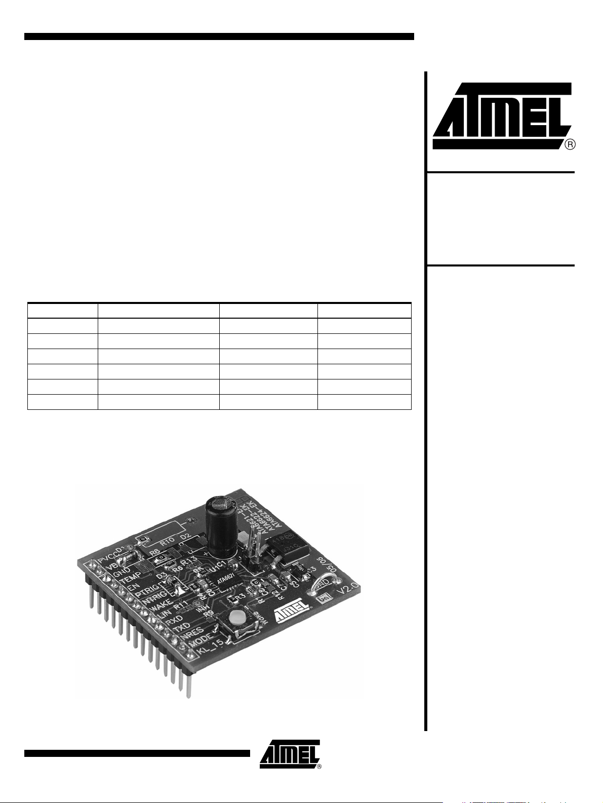
Figure 1-1. ATA6621/22/24 Development Board
Board
Application Note
4970A–AUTO–01/07
Page 2
Another difference is unequal watchdog timing (see Section 2.3 on page 4).
The combination of the features included in the ATA6621/22/24 makes it possible to develop
simple, but powerful and cheap, slave nodes in LIN-bus systems.
The ICs are designed to handle the low-speed data communication in vehicles, for example, in
convenience electronics. Improved slope control at the LIN driver ensures secure data communication up to 20 Kbaud.
Sleep Mode and Silent Mode guarantee a very low current consumption.
This document has been developed to give the user an easy start with the development board
of the ATA6621/22/24. For more detailed information about the use of these devices themselves, refer to the corresponding datasheets.
1.1 Development Board Features
The development board for the ATA6621/22/24 supports the following features:
• All necessary components to put the ATA6621/22/24 in operation are included
• Placeholders for some optional components for extended functions included
• All pins easily accessible
• Easily adaptable watchdog times by replacing a resistor
• Possibility to place an external NPN transistor for boosting up the output current of the
voltage regulator (jumper J1)
• Possibility of selecting between master or slave operation (mounting D3 and R4)
1.2 Quick Start
The development board for the ATA6621/22/24 is shipped with all necessary components and
a default jumper setting to start with the development of a LIN slave node immediately.
After connecting an external 12V DC power supply between the terminals VB and GND, the
circuit is in the Pre-normal mode (Fail Safe mode) and a 5V (3.3V) DC voltage provided by the
internal voltage regulator can be measured between VCC and GND. (The Pre-normal mode is
called Fail Safe mode in the datasheets of the devices ATA6622 and ATA6624.) Furthermore,
the following voltages or states can be measured at the pins WD_OSC, TEMP, INH, RXD and
LIN:
Table 1-2. ATA6621
Mode VCC WD_OSC TEMP INH RXD LIN Transceiver
Pre-normal mode 5V 2.5V ~2V - 5V Recessive Off
Normal mode 5V 2.5V ~2V - 5V Recessive On
Table 1-3. ATA6622
Mode VCC WD_OSC TEMP INH RXD LIN Transceiver
Fail Safe mode 3.3V 1.23V - On 3.3V Recessive Off
Normal mode 3.3V 1.23V - On 3.3V Recessive On
2
ATA6621/22/24 Development Board
4970A–AUTO–01/07
Page 3

ATA6621/22/24 Development Board
Table 1-4. ATA6624
Mode VCC WD_OSC TEMP INH RXD LIN Transceiver
Fail Safe mode 5V 1.23V - On 5V Recessive Off
Normal mode 5V 1.23V - On 5V Recessive On
As the window watchdog of the ATA6621/22/24 is already active in the Pre-normal mode (Fail
Safe mode), a periodic reset signal will be generated at the pin NRES as long as no trigger
signal can be received at the watchdog trigger input. Normally the connected microcontroller
will be monitored by the watchdog, so it has to generate the required trigger signal as
described in Section 2.3 on page 4 and in more detail in the datasheet of the corresponding
device. For the quick start it is sufficient to generate a square-wave signal with V
f = 75Hz at pin NTRIG or PTRIG for the ATA6621 or with f = 50Hz at pin NTRIG for the
ATA6622 and ATA6624 (this is recommended only for testing purposes). In order to check
that the watchdog is triggered in the expected way, the reset pin NRES can be monitored until
a continuous high level is available.
Please note that the communication is still inactive in Pre-normal mode (Fail Safe mode).
In order to communicate via the LIN bus interface you have to switch to normal mode by
applying the VCC voltage (5V or 3.3V, as appropriate) at pin EN.
= VCC and
PP
2. Hardware Description
In the following sections only the normal operating conditions will be described. For further
information concerning one of the mentioned features, refer to the corresponding datasheet.
2.1 Power Supply (VB and GND)
In order to get the development board running, an external 5.7V to 18V DC power supply is
required between the terminals VB and GND. The input circuit is protected against
inverse-polarity with the protection diode D1, so that there is normally a difference between
the VB and VS level of approximately 0.7V.
2.2 Voltage Regulator (PVCC and VCC)
The internal 5V/3.3V voltage regulator is capable of driving loads with up to 50 mA current
consumption so the SBCs are able to supply a microcontroller, sensors and/or other ICs. The
voltage regulator is protected against overloads by means of current limitation and overtemperature shutdown. To boost the maximum load current, an external NPN transistor may be
used, with its base being connected to the VCC pin and its emitter connected to PVCC. If this
is done, the regulated output voltage of 5V or 3.3V is available at pin PVCC. For this reason,
the pin PVCC and not the pin VCC is led to the connector available off the board.
But in normal operation, the pins PVCC and VCC have to be connected directly. This is done
by setting jumper J1.
4970A–AUTO–01/07
3
Page 4
2.3 The Window Watchdog (PTRIG, NTRIG and NRES)
s
The watchdog anticipates a trigger signal from the microcontroller at the NTRIG input (negative edge) within a defined time window. The ATA6621 has an additional PTRIG input, so it is
also possible to trigger the watchdog with a positive edge. If no correct trigger signal is
received, a reset signal will be generated at the NRES output. During Silent or Sleep Mode the
watchdog is switched off to reduce current consumption.
The minimum time for the first watchdog pulse is required after the undervoltage reset at the
NRES pin disappears and is defined as lead time t
The timing basis of the watchdog is provided by the internal oscillator, whose time period t
is adjustable via the external resistor R3 at the pin WD_OSC. For the ATA6621, the voltage at
this pin is 2.5V, for the ATA6622 and ATA6624 it is 1.23V (see Table 1-2 on page 2 through
Table 1-4 on page 3). Due to these different voltages at the devices, the resulting timings are
also different. There is a resistor R3 with a value of 51 kΩ mounted on the development board,
which results in the following timing sequence for the ATA6621:
Figure 2-1. Timing Sequence with R3 = 51 kΩ at the ATA6621
= 5V
V
CC
Undervoltage Reset Watchdog Reset
= 10 ms
t
NRES
reset
.
d
OSC
t
= 1.9 m
nres
NTRIG
PTRIG
td = 49 ms
= 10 ms
t
1
t
trigg
t
t
wd
> 3 µs
= 10.5 ms
2
t
1
t
2
4
ATA6621/22/24 Development Board
4970A–AUTO–01/07
Page 5
ATA6621/22/24 Development Board
t
For the ATA6622 and ATA6624 the resistor R3 at pin WD_OSC with the same value of 51 kΩ
results in the different timing sequence shown in Figure 2-2:
Figure 2-2. Timing Sequence with R3 = 51 kΩ at the ATA6622 and ATA6624
= 3.3V/5V
V
CC
Undervoltage Reset Watchdog Rese
t
= 4 ms
NRES
reset
t
nres
= 4 ms
td = 150 ms
NTRIG
If you want to change the watchdog times mentioned above it is only necessary to change the
value of the external resistor R3 (refer to the corresponding datasheet).
2.4 LIN Interface (LIN, TXD and RXD)
2.4.1 Bus Pin (LIN)
A low-side driver with internal current limitation and thermal shutdown as well as an internal
pull-up resistor in compliance with the LIN specification 2.0 is implemented. LIN receiver
thresholds are compatible with the LIN protocol specification.
At the LIN pin there is a 220-pF capacitor to ground on the board. Additionally, when using the
development board for a LIN master application, there is the opportunity to mount the two necessary extra components diode D2 (LL4148) in series with resistor R1 (1kΩ) on the board at
their designated placeholders.
= 20 ms
t
1
t
trigg
= 21 ms
t
2
t
wd
> 200 ns
t
1
t
2
2.4.2 Input Pin (TXD)
2.4.3 Output Pin (RXD)
4970A–AUTO–01/07
This pin is the microcontroller interface to control the state of the LIN output. TXD must be
pulled to ground in order to have the LIN bus low. If TXD is high, the LIN output transistor is
turned off and the bus is in the recessive state, pulled up by the internal resistor. If TXD is low,
the LIN output transistor is turned on and the bus is in the dominant state. An internal timer
prevents the bus line from being driven permanently in the dominant state. If TXD is forced to
low longer than t
> 20 ms, the LIN bus driver is switched to the recessive state.
DOM
This pin reports the state of the LIN bus to the microcontroller. LIN high (recessive state) is
reported by a high level at RXD, LIN low (dominant state) is reported by a low level at RXD.
The output has an internal pull-up structure with typ. 5 kΩ to VCC.
The output is short-circuit protected.
5
Page 6

2.5 Temp Pin (TEMP) (ATA6621 Only)
Besides the internal temperature monitoring of the voltage regulator, an additional sensor
measures the junction temperature and provides a linearized voltage at the TEMP pin.
Together with the analog functions of the microcontroller (for example, the analog comparator
and/or the analog-to-digital converter), this enables the application to detect overload conditions. Further actions in order to prevent the IC from damage can be implemented.
2.6 Mode and TM Input Pins (MODE and TM)
The TM input is only used for Atmel® internal-testing purposes and therefore connected
directly to GND. The Mode input is pulled to GND by the 4.7-kΩ resistor R1 and therefore the
watchdog is active in the normal operation mode. Especially during the early development
phase it can be helpful to have the possibility to deactivate the watchdog in order to debug the
application program without disturbing RESETS caused by the watchdog. Therefore the
watchdog can be switched off by connecting the MODE pin to VCC externally.
2.7 Reset Output (NRES)
After ramping up the battery voltage or after a wake-up from Sleep mode, the 5V regulator is
switched on and the VCC voltage exceeds the undervoltage threshold. The implemented undervoltage delay keeps the NRES output at low level for approximately 10 ms after VCC
reaches its nominal value. Then it switches to high and the watchdog waits for the trigger
sequence from the microcontroller.
The NRES pin switches to low if the watchdog is not triggered correctly (see Section 2.3 on
page 4).
In the ATA6621 the Reset output is a push-pull state supplied by the VCC voltage.
In the ATA6622 and ATA6624, the Reset output is an open drain output implemented with a
single MOS transistor which is switched on in case of a VCC undervoltage or if the watchdog
is not triggered correctly. In order to pull up the NRES output of the ATA6622/24 an external
resistor connected to VCC
opment board.
If a reset occurs (NRES is Low), the circuit switches to Pre-normal mode (Fail Safe mode).
is necessary. This resistor (R9) is taken into account on the devel-
2.8 KL_15 Input (KL_15) (ATA6622/24 Only)
This pin is a high voltage input used to wake up the device from Sleep or Silent mode. It is an
edge sensitive pin (rising edge). It is usually connected to the ignition in order to generate a
local wake-up in the application if the ignition is switched on. To protect the pin against voltage
transients, a series resistor R12 and a 100-nF ceramic capacitor C8 have to be used. If this
pin is not needed, it must be connected to GND.
2.9 Inhibit Output (INH) (ATA6622/24 Only)
This pin is a high-side switch and it is normally used to switch on an external voltage regulator
during Normal mode or Fail Safe mode. In Sleep mode or Silent mode the INH output is
switched off.
For master node applications it is possible to switch off the external master resistor (R4) by the
INH pin.
6
ATA6621/22/24 Development Board
4970A–AUTO–01/07
Page 7

3. Boosting the Voltage Regulator
For some applications there is a need for a higher current than the internal voltage regulator
can deliver (50 mA). So it is possible to boost the maximum current by using an external NPN
transistor. On the development board there is already a placeholder for this part, into which
would fit, for example, the MJD31C in a D-PAK package. In addition to the transistor itself
there are two more components to be placed on the development board, the resistor R7 (3.3Ω)
and the electrolytic capacitor C4 (2.2 µF). The jumper J1 has to be removed in this case.
Note that the output voltage is no longer short-circuit protected when boosting the output current with an external NPN transistor.
The limiting parameter for the output current is the maximum power dissipation of the external
NPN transistor. In the version at this stage the thermal resistance of the MJD31C soldered on
the minimum pad size is 80 K/W, meaning the maximum possible output current in the case of
V
= 12V is approximately 230 mA at room temperature. It is not recommended to exceed this
S
limit, because the transistor could be damaged as a result of overtemperature. If a higher output current is required, additional cooling of the external transistor has to be ensured (see
Figure 3-2, Figure 3-3 and Figure 3-4 on page 8).
Figure 3-1. Boosting the Voltage Regulator
ATA6621/22/24 Development Board
Place T1, R7 and C4 and remove jumper J1 when boosting the output current
4970A–AUTO–01/07
7
Page 8

Figure 3-2, Figure 3-3 and Figure 3-4 show the maximum output current (I
regulator as a function of the supply voltage (V
(R
) of the external NPN transistor T1.
thJA
) at different coolings or thermal resistances
S
) of the voltage
max
Figure 3-2. I
Figure 3-3. I
versus VS at R
max
350
300
250
200
(mA)
150
max
I
100
50
0
versus VS at R
max
600
500
400
300
(mA)
max
200
I
= 80 K/W (No Additional Cooling)
thJA
Ta = 25˚C
T
= 85˚C
a
T
= 125˚C
a
10 12 14 16 18 20
VS (V)
= 50 K/W (Additional Cooling)
thJA
= 25˚C
T
a
T
= 85˚C
a
Figure 3-4. I
100
versus VS at R
max
1400
1200
1000
800
(mA)
600
max
I
400
200
T
= 125˚C
0
10 12 14 16 18 20
a
VS (V)
= 20 K/W (Additional Cooling)
thJA
= 25˚C
T
a
= 85˚C
T
a
= 125˚C
T
0
10 12 14 16 18 20
a
VS (V)
8
ATA6621/22/24 Development Board
4970A–AUTO–01/07
Page 9

ATA6621/22/24 Development Board
Figure 3-5 to Figure 3-10 on page 11 show some typical operating characteristics measured at
the ATA6621. The supply voltage V
(reverse battery protection). The external circuitry is shown in Figure 4-1 on page 12.
is approximately a diode forward voltage lower than V
S
bat
Figure 3-5. Output Voltage PV
ATA6621 with External Boosttransistor MJD31C
6
5
4
(V)
3
CC
PV
2
1
0
024681012
Figure 3-6. Output Voltage PV
5.020
5.0 15
5.0 10
(V)
CC
5.005
PV
5.000
4.995
versus Battery Voltage V
CC
I
= 0
OUT
I
= 20 mA
OUT
V
(V)
bat
versus Battery Voltage V
CC
at Startup
bat
at Different Output Currents
bat
ATA6621 with External Boosttransistor MJD31C
= 0
I
OUT
I
= 20 mA
OUT
I
= 100 mA
OUT
4970A–AUTO–01/07
4.990
01020304050
V
(V)
bat
9
Page 10

Figure 3-7. Load- transient Response Ch1: I
, Ch2: PV
OUT
CC
Figure 3-8. Startup Response Ch1: VS, Ch2: PV
CC
10
ATA6621/22/24 Development Board
4970A–AUTO–01/07
Page 11

ATA6621/22/24 Development Board
Figure 3-9. Switching from Silent to Normal Mode Ch1: NRES, Ch2: PV
CC
Figure 3-10. Output Voltage PVCC versus Temperature at Different Load Currents
5,05
5,04
5,03
5,02
(V)
CC
5,01
PV
5,00
4,99
4,98
-40-200 20406080100120
I
= 100 mA
OUT
I
OUT
= 20 mA
Temperature (˚C)
= 0
I
OUT
4970A–AUTO–01/07
11
Page 12

4. Schematic and Layout of the Development Board for the ATA6621/22/24
Figure 4-1. Schematic of the Development Board for the ATA6621/22/24
PVCC
VBAT
D1
LL4148
V1
R8
100Ω/1W
R8b
0
VS
R10
10Ω/2W
R10b
0
GND
TEMP
EN
PTRIG
NTRIG
WAKE
LIN
RXD
TXD
TEMP
D2
BZG04-33
+
+
C3
10 µF
C2
22 µF/50V
C1
100 nF
C5
100 nF
R6
10 kΩ
R13
S1
Wake
J1
VCC
0
R5
33 kΩ
R7
3.3Ω
EN
PTRIG
NTRIG
WAKE
GND
+
C4
2.2 µF
VS
20 19 18
1
2
3
4
5
67 8 109
NC
VCC
GND
GND
LIN
T1
MJD31C
PVCC
17
ATA6621/
ATA6622/
ATA6624
GND
NC
TEMP
GND
RXD
GND
16
KL15INH
NC
TEMP
15
14
13
12
11
R11
47 kΩ
C7
1 nF
MODE
TM
WD_OSC
NRES
TXD
(ATA6622/24)
R12
47 kΩ
MODE
R3
51 kΩ
KL_15
LL4148
C8
100 nF
R1
4.7 kΩ
R9
PVCC
10 kΩ
INH
(ATA6622/24)
220 pF
D3
R4
1 kΩ
LIN
C6
NRES
MODE
KL_15
12
MODE
KL_15
X1
Notes: 1. D3 and R4 are only necessary for a master node.
2. R9 and R13 are only needed for ATA6622 and ATA6624.
3. Pin KL_15 and the corresponding external circuitry are only available at the ATA6622/24.
4. Pin INH and the corresponding external circuitry are only available at the ATA6622/24.
5. Pin 17 has to be connected to GND by replacing C7 with a 0Ω resistor at ATA6622 or
ATA6624.
6. ATA6621: Pin 10 has to be connected to GND via R11 = 0. Pin 16 has to be connected to
GND by replacing C8 by a 0Ω resistor.
ATA6621/22/24 Development Board
ATA6621-EK
ATA6622-EK
ATA6624-EK
Revision 2.0
4970A–AUTO–01/07
Page 13

ATA6621/22/24 Development Board
Figure 4-2. ATA6621/22/24 Board Component Placement; Top Side, Top View
Figure 4-3. ATA6621/22/24 Development Board; Top Side, Top View
4970A–AUTO–01/07
13
Page 14
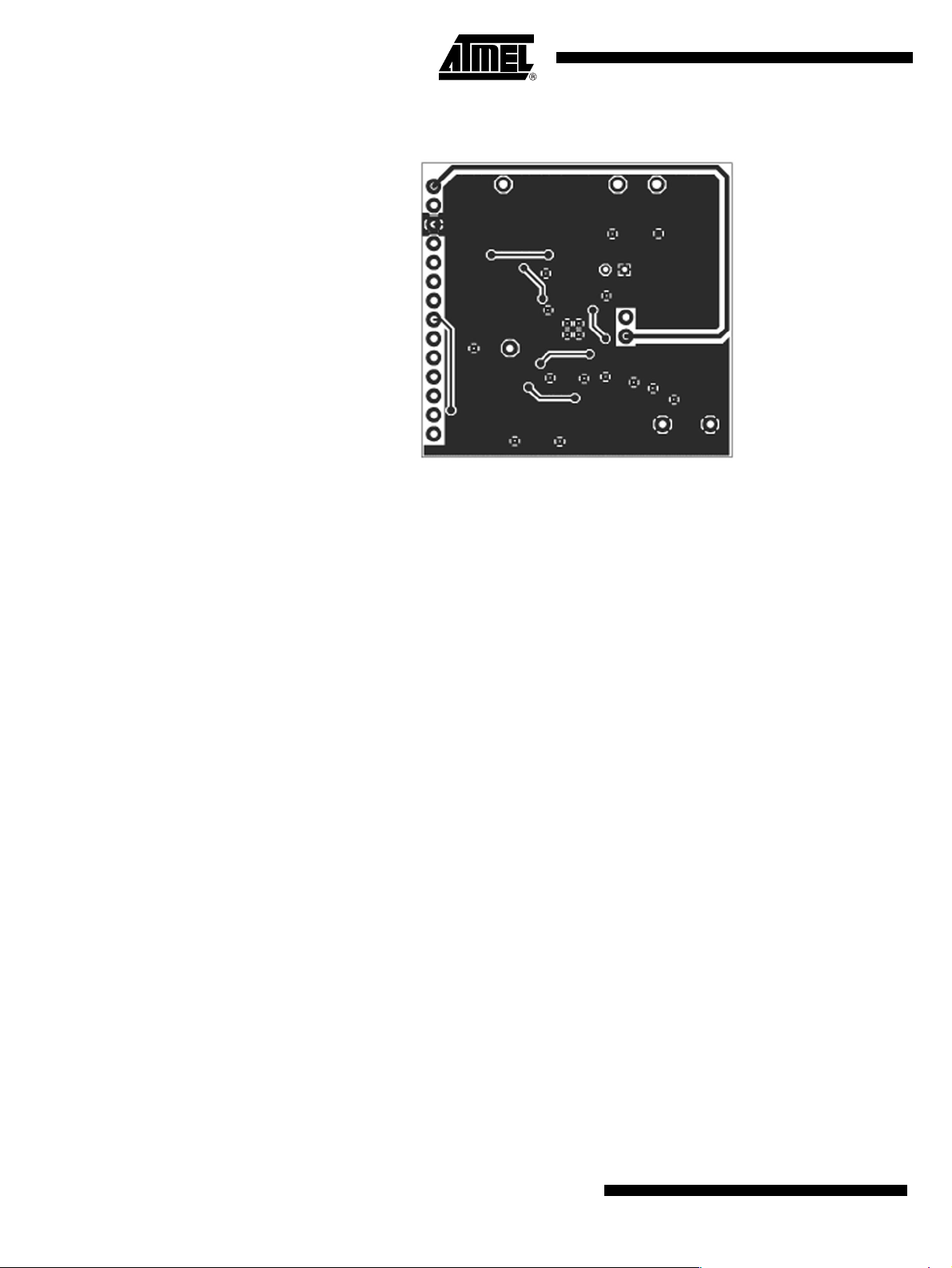
Figure 4-4. ATA6621/22/24 Development Board; Bottom Side, Top View (as if PCB Were
Transparent)
14
ATA6621/22/24 Development Board
4970A–AUTO–01/07
Page 15

ATA6621/22/24 Development Board
5. The Development Board in a Simple Application
To show just how easy it is to develop a LIN-based application with the development board for
the ATA6621/22/24, here is a little example for a complete LIN slave node consisting of the
ATA6621 and the microcontroller ATmega88, a flasher controlled via the LIN bus.
The LIN interface of the slave is implemented with the ATA6621 and the control of the flasher
as well as the protocol handling is done by the ATmega88 microcontroller. In the schematic of
this slave node it is obvious that there are almost no other external components needed to fulfill the requirements of this application, other than the development board of the
ATA6621/22/24 and the ATmega88.
Figure 5-1. Simple Application Using the Development Board for the ATA6621/22/24 (Schematic)
X4
X5
X6
X7
NRES
X1
VS
TEMP
EN
NTRIG
LIN
RXD
TXD
VS
LIN
XISP1
ISP
JP1
S1
JP2
Development board
ATA6621/6622/6624
330Ω
PVCCPB4
PB3PB5
PVCC
NRES
R1
LED1
PVCC
330Ω
LEDLED
D2D1
R2
LED2
PVCC
100 nF
C1
PD3
PD4
GND (3)
VCC (4)
GND (5)
VCC (6)
PB6
PB7
Flasher
TXD
PD2
PD1
32 31 30 28
1
2
3
4
5
91011 1312
LED2
PC5
PD0
PC6/NRST
29
U1
ATMEGA88
MLF 5 mm × 5 mm
0.5 mm pitch
32 lead
PB1
NTRIGRXD
PC4
PC3
1427152616
ENLED1NRES
PC2
25
XL1
XL2
R5
1 kΩ
24
23
22
21
20
196
187
178
VS
+
100 µF
T1
BC817-40
PC1
PC0
ADC7
GND (21)
AREF
ADC6
AVC C
PB5
GND (33)
C8
100 nF
C6
C4
100 nF
PB5
TEMP
C7
10 µF
PVCC
C5
100 nF
+
4970A–AUTO–01/07
PD5
PD6
PD7
PB1
PB0
PB1 PB4PB3
PB2
PB3
PB4
15
Page 16

For testing purposes two jumpers (JP1 and JP2) have been added to the LIN part of this application in order to have the opportunity to easily change some parameters at the pins NRES
and VCC/PVCC. Additionally, the switch S1 has been included to generate a wake pulse.
For the microcontroller part of this slave node, only a few blocking capacitors are necessary.
XISP1 is the programming interface and D1, D2, R1 and R2 report the internal status of the
slave node. Because the flasher runs with 12V DC, the transistor T1 is needed to transfer the
5V from the microcontroller to the 12V level. Furthermore, the flasher produces some glitches,
so that there are some capacitors needed in order to block the 12V power supply.
Figure 5-2. A Simple Application Using the Development Board for the ATA6621
(Photograph)
16
ATA6621/22/24 Development Board
4970A–AUTO–01/07
Page 17

Atmel Corporation Atmel Operations
2325 Orchard Parkway
San Jose, CA 95131, USA
Tel: 1(408) 441-0311
Fax: 1(408) 487-2600
Regional Headquarters
Europe
Atmel Sarl
Route des Arsenaux 41
Case Postale 80
CH-1705 Fribourg
Switzerland
Tel: (41) 26-426-5555
Fax: (41) 26-426-5500
Asia
Room 1219
Chinachem Golden Plaza
77 Mody Road Tsimshatsui
East Kowloon
Hong Kong
Tel: (852) 2721-9778
Fax: (852) 2722-1369
Japan
9F, Tonetsu Shinkawa Bldg.
1-24-8 Shinkawa
Chuo-ku, Tokyo 104-0033
Japan
Tel: (81) 3-3523-3551
Fax: (81) 3-3523-7581
Memory
2325 Orchard Parkway
San Jose, CA 95131, USA
Tel: 1(408) 441-0311
Fax: 1(408) 436-4314
Microcontrollers
2325 Orchard Parkway
San Jose, CA 95131, USA
Tel: 1(408) 441-0311
Fax: 1(408) 436-4314
La Chantrerie
BP 70602
44306 Nantes Cedex 3, France
Tel: (33) 2-40-18-18-18
Fax: (33) 2-40-18-19-60
ASIC/ASSP/Smart Cards
Zone Industrielle
13106 Rousset Cedex, France
Tel: (33) 4-42-53-60-00
Fax: (33) 4-42-53-60-01
1150 East Cheyenne Mtn. Blvd.
Colorado Springs, CO 80906, USA
Tel: 1(719) 576-3300
Fax: 1(719) 540-1759
Scottish Enterprise Technology Park
Maxwell Building
East Kilbride G75 0QR, Scotland
Tel: (44) 1355-803-000
Fax: (44) 1355-242-743
RF/Automotive
Theresienstrasse 2
Postfach 3535
74025 Heilbronn, Germany
Tel: (49) 71-31-67-0
Fax: (49) 71-31-67-2340
1150 East Cheyenne Mtn. Blvd.
Colorado Springs, CO 80906, USA
Tel: 1(719) 576-3300
Fax: 1(719) 540-1759
Biometrics
Avenue de Rochepleine
BP 123
38521 Saint-Egreve Cedex, France
Tel: (33) 4-76-58-47-50
Fax: (33) 4-76-58-47-60
Literature Requests
www.atmel.com/literature
Disclaimer: The information in this document is provided in connection with Atmel products. No license, express or implied, by estoppel or otherwise, to any
intellectual property right is granted by this document or in connection with the sale of Atmel products. EXCEPT AS SET FORTH IN ATMEL’S TERMS AND CONDI-
TIONS OF SALE LOCATED ON ATMEL’S WEB SITE, ATMEL ASSUMES NO LIABILITY WHATSOEVER AND DISCLAIMS ANY EXPRESS, IMPLIED OR STATUTORY
WARRANTY RELATING TO ITS PRODUCTS INCLUDING, BUT NOT LIMITED TO, THE IMPLIED WARRANTY OF MERCHANTABILITY, FITNESS FOR A PARTICULAR
PURPOSE, OR NON-INFRINGEMENT. IN NO EVENT SHALL ATMEL BE LIABLE FOR ANY DIRECT, INDIRECT, CONSEQUENTIAL, PUNITIVE, SPECIAL OR INCIDENTAL DAMAGES (INCLUDING, WITHOUT LIMITATION, DAMAGES FOR LOSS OF PROFITS, BUSINESS INTERRUPTION, OR LOSS OF INFORMATION) ARISING OUT
OF THE USE OR INABILITY TO USE THIS DOCUMENT, EVEN IF ATMEL HAS BEEN ADVISED OF THE POSSIBILITY OF SUCH DAMAGES. Atmel makes no
representations or warranties with respect to the accuracy or completeness of the contents of this document and reserves the right to make changes to specifications
and product descriptions at any time without notice. Atmel does not make any commitment to update the information contained herein. Unless specifically provided
otherwise, Atmel products are not suitable for, and shall not be used in, automotive applications. Atmel’s products are not intended, authorized, or warranted for use
as components in applications intended to support or sustain life.
© 2007 Atmel Corporation. All rights reserved. Atmel®, logo and combinations thereof, Everywhere You Are® and others are registered trade-
marks or trademarks of Atmel Corporation or its subsidiaries. Other terms and product names may be trademarks of others.
4970A–AUTO–01/07
 Loading...