

Page 1

Features
• Programmable AVR
• Frequency: 315 MHz (ATA6285) and 433 MHz (ATA6286)
• Support ASK/FSK Modulation with Integrated FSK Switch
• 6 dBm Output Power with Typically 8.5 mA Active Current Consumption in
Transmission Mode
• Low-power Microcontroller Requires Typically 0.6 µA Sleep Current with Active Interval
Timer
• Interfaces for Simple Capacitive Sensors (2 pF to 6 pF)
• One Interface Can Be Configured for Motion Wake-up (3 pF to 5 pF)
• Typically 25 mbar ADC Resolution for Pressure Measurement with Dedicated Sensor
Type
• Low-power Measurement Mode for Directly Connected Capacitive Sensors Typically
200 µA at 1 MHz System Clock
• Programmable 125 kHz Wake-up Receiver Channel with Typically 1.7 µA Current
Consumption in Listing Mode
• 2V to 3.6V Operation Voltage for Single Li-cell Power Supply
• –40°C to +125°C Operation Temperature and –40°C to +150°C Storage Temperature
• Less then 10 External Passive Components
• QFN32 (5 mm × 5 mm) Package
®
8-bit Flash Microcontroller Transmitter IC
TPMS Control
and Transmitter
IC
ATA6285
ATA6286
1. Description
ATA6285 and ATA6286 are highly integrated smart RF micro transmitter ICs for
315 MHz and 433 MHz, suited for ASK and FSK with typically 20 Kbits/s data rate in
Manchester mode. The devices combine the functionality of the RF transmitter ICs
ATA5756/ATA5757 with the programmable low-power AVR 8-bit Flash microcontroller
in a single QFN32 package (5 mm × 5 mm). The ATA6285 and ATA6286 include a
dedicated ADC interface for simple capacitive sensors as well as an on-chip temperature sensor. Three sensor interfaces are available for a capacitive range of 2 pF to
16 pF, where one channel can be configured as motion wake-up in the range of 3 pF
to 5 pF. The ICs are suited for use in tire pressure monitoring (TPMS) sensor gauges
in combination with external sensor devices.
The programmable AVR 8-bit Flash microcontroller includes 8 Kbytes of in-system
self-programmable Flash memory and an 320-Bytes EEPROM, thus allowing the system integrator to install field-programmable firmware to enable system flexibility on
different platforms. ATA6285 and ATA6286 can be configured to guarantee extremely
low power consumption in sleep mode and measurement mode. They also include a
programmable 125 kHz wake-up receiver channel for extremely low current consumption in listening mode. The ICs are designed for use in applications with typically less
then 10 passive components: one external crystal for the sensor gauge, several
capacitors, a single LiMnO2 battery coin cell, a single-ended antenna for the data
transmission and an LF ferrite coil for the wake-up channel. ATA6285 and ATA6286
support TPMS-specific low-current modes even with an active brown-out detection
and an interval timer.
Summary
Preliminary
NOTE: This is a summary document.
The complete document is available
under NDA. For more information,
please contact your local Atmel sales
office.
4958AS–AUTO–09/06
Page 2
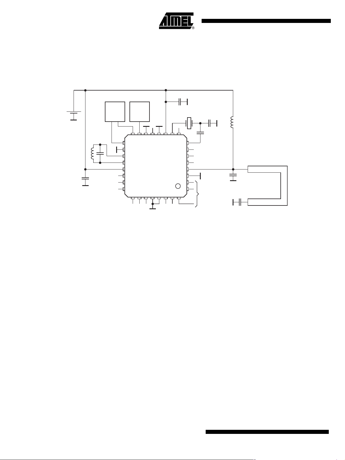
2. Overview
2.1 Application
Figure 2-1. Tire Pressure Monitoring System (TPMS)
VDD
Battery
XZ
Motion
sensor
Pressure
sensor
16 15 14 13
17
18
19
20
21
22
23
24
25 26 27 28 29 30 31 32
12 11 10 9
ATA6285/
ATA6286
*)
ISP:
8
7
6
5
4
3
2
1
*)
ISP interface
In-System-Programmable
Flash interface
Crystal Frequency 13.56 MHz for 433 MHz application
Crystal Frequency 13.125 MHz for 315 MHz application
RF
loop antenna
2
ATA6285/ATA6286 [Preliminary]
4958AS–AUTO–09/06
Page 3
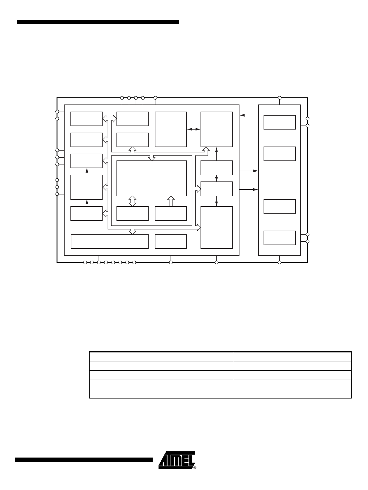
2.2 Block Diagram
Figure 2-2. ATA6285/ATA6286 Block Diagram (MCP)
ATA6285/ATA6286 [Preliminary]
LF1
LF2
S0
S1
S2
PC2
PC1
PC0
LF Receiver
125 kHz
Voltage
monitor
Timer block
Sensor
interface/
input
multiplexer
Temperature
sensor
PB7 (NSS)
PB5 (SCK)
PB4 (MISO)
PB3 (MOSI)
SPI
EEPROM
SRAM
IO Ports debugWIRE
VCC
Oscillator
AVR Core
Flash
ECIN1
Clock
management
and
monitoring
Watchdog
oscillator
Watchdog
timer
Power
Supervision
POR/ BOD/
TSD and
RESET
CLOCK
ASK
FSK
VSRF
XTO
PLL
RF
Transmitter
VCO
Power
amplifier
XTO1
XTO2
ANT1
ANT2
PB1 (T3O)
PB0 (T3ICP)
2.3 Inter-die Bonding
The ATA6285/ATA6286 are Smart RF Micro Transmitter ICs in MCP (Multi Chip Package) technology. Table 2-1 shows the internal assembly of the MCP.
Table 2-1. Inter-die Connection Description of the MCP
AVR – Pin ATA5756/ATA5757 – Pin
PD3 (INT1) – External interrupt input 1 EN – Enable input
PD4 (ECIN1) – External clock input 1 CLK – Clock output signal
PD5 (T2O1) – Timer2 modulator output 1 ASK – Input signal
PD6 (T2O2) – Timer2 modulator output 2 FSK – Input signal
PB6
PB2 (T2I)
PD1 (T3I)
PD2 (INTO)
PD0 (T2ICP)
PD7 (SDIN)
GND
NRESET
GNDRF
4958AS–AUTO–09/06
3
Page 4
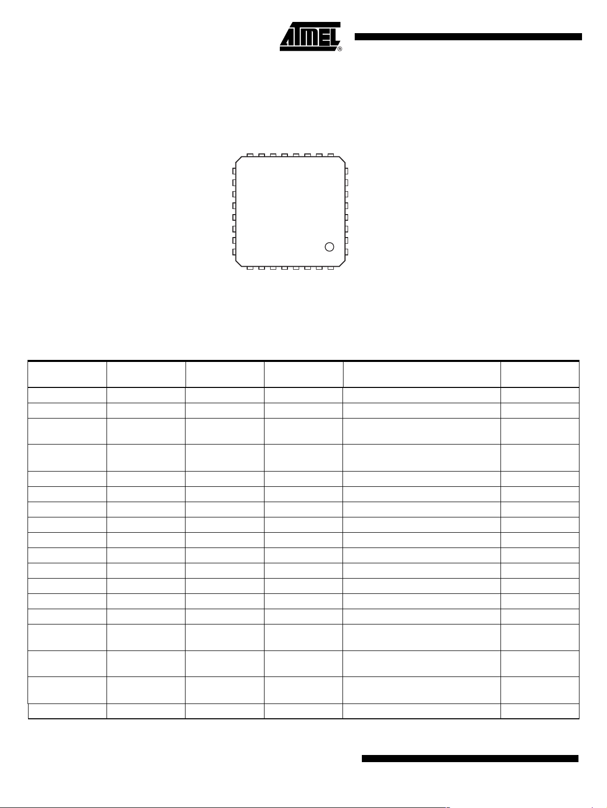
2.4 Pin Configuration
Figure 2-3. Pinning QFN32
S2
GND
LF1
LF2
VCC
PC2
PC1
PC0
Table 2-2. Pin Description
Alternate
Pin Number Pin Name
1 PB4 MISO PCINT4 SPI Port B4
2 PB5 SCK PCINT5 SPI Port B5
3ANT2– –
4ANT1– –
5 PB1 T3O PCINT1 Timer3 output Port B1
6 PB6 – PCINT6 Port B6
7 PB7 NSS PCINT7 SPI Port B7
8 XT02 – – Switch for FSK modulation RF pin
9 PB2 T2I PCINT2 Timer2 external input clock Port B2
10 XT01 – – Connection for crystal RF pin
11 VS_RF – – Power supply voltage for RF RF pin
12 GND – – Power supply ground for RF RF pin
13 NRESET debugWIRE – Reset input/debugWIRE interface
14 GND – – Power supply ground
15 S0 – –
16 S1 – –
17 S2 – –
18 GND – – Power supply ground
Note: 1. Internal inter-die connection of the MCP
Function 1
S1
S0
NRESET
GND
GND
16
15 14 13
17
18
19
20
ATA62857
21
22
23
24
ATA6286
25 26 27 28 29 30 31 32
PD1 (T3I)
PB0 (T3ICP)
PD0 (T2ICP)
VSRF
12 11 10 9
GND
GND
PD7 (SDIN)
Alternate
Function 2 Function Comment
PB2 (T2I)
XTO1
8
XTO2
7
PB7 (NSS)
6
PB6
5
PB1 (T3O)
4
ANT1
3
ANT2
2
PB5 (SCK)
1
PB4 (MISO)
PD2 (INTO)
PB3 (MOSI)
RF-antenna 2. Emitter of antenna
output stage
RF-antenna 1. Open collector
antenna output
Sensor input 0 – Pressure Sensor
(Cap.)
Sensor input 1 – X – Motion Sensor
(Cap.)
Sensor input 2 – Z - Motion Sensor
(Cap.)
RF pin
RF pin
4
ATA6285/ATA6286 [Preliminary]
4958AS–AUTO–09/06
Page 5

Table 2-2. Pin Description (Continued)
Alternate
Pin Number Pin Name
19 LF1 – – LF-receiver input 1
20 LF2 – – LF-receiver input 2
21 V
22 PC2 – PCINT10 - Port C2
23 PC1 CLKO PCINT9 System clock output Port C1
24 PC0 ECIN0 PCINT8 External Clock input 0 Port C1
25 PD0 T2ICP PCINT16 Timer2 external input capture Port D0
26 PD1 T3I PCINT17 Timer3 external input clock Port D1
27 PB0 T3ICP PCINT0 Timer3 external input capture Port B0
28 GND – – Power supply ground
29 GND – – Power supply ground
Inter-die
Inter-die
Inter-die
Inter-die
Note: 1. Internal inter-die connection of the MCP
(1)
(1)
(1)
(1)
30 PD7 SDIN PCINT23 SSI –Serial Data Input Port D7
31 PD2 INT0 PCINT18 External interrupt input 0 Port D2
32 PB3 MOSI PCINT3 SPI Port B3
CC
PD3 INT1 PCINT19
PD4 ECIN1 PCINT20
PD5 T2O1 PCINT21
PD6 T2O2 PCINT22
Function 1
– – Power supply voltage (VCC + AVCC)
ATA6285/ATA6286 [Preliminary]
Alternate
Function 2 Function Comment
External Interrupt 1
connection
External Clock input 1
connection
Timer2 Modulator output 1
Inter-die connection
Timer2 Modulator output 2
Inter-die connection
→Inter-die
→Inter-die
→
→
Por t D2
Por t D4
Por t D5
Por t D6
2.5 Pin Names
2.5.1 VCC
2.5.2 GND
2.5.3 Port B (PB7..0)
4958AS–AUTO–09/06
Supply voltage
Ground
Port B is a 5(8)-bit bi-directional I/O port with internal pull-up resistors (selected for each bit). The
PB7, PB6 and PB2 ports are only used as internal I/O ports for inter-die connections. The Port B
output buffers have symmetrical drive characteristics with both high sink and source current
capability. As inputs, Port B pins that are externally pulled low will source current if the pull-up
resistors are activated. The Port B pins are tri-stated when a reset condition becomes active,
even if the clock is not running.
Port B also serves the functions of various special features of the ATmegaT.
5
Page 6

2.5.4 Port C (PC2..0)
2.5.5 Port D (PD7..0)
2.5.6 NRESET
2.5.7 LF (2..1)
Port C is a 3-bit bi-directional I/O port with internal pull-up resistors (selected for each bit). The
Port C output buffers have symmetrical drive characteristics with both high sink and source current capability. As inputs, Port C pins that are externally pulled low will source current if the
pull-up resistors are activated. The Port C pins are tri-stated when a reset condition becomes
active, even if the clock is not running.
Port D is a 7(1)-bit bi-directional I/O port with internal pull-up resistors (selected for each bit).
The PD(6..3) pins are used as internal inter-die connection I/O ports. The Port D output buffers
have symmetrical drive characteristics with both high sink and source current capability. As
inputs, Port D pins that are externally pulled low will source current if the pull-up resistors are
activated. The Port D pins are tri-stated when a reset condition becomes active, even if the clock
is not running.
Port D also serves the functions of various special features of the ATmegaT.
Reset input. A low level on this pin for longer than the minimum pulse length will generate a
reset, even if the clock is not running. Shorter pulses then defined minimum pulse length are not
guaranteed to generate a reset.
Input coil pins for the LF-Receiver.
2.5.8 S (2..0)
2.5.9 ANT(2, 1)
2.5.10 XTO(0, 1)
Measuring input pins for external capacitance sensor elements.
RF-Antenna pins.
External crystal for the internal RF transmitter IC.
6
ATA6285/ATA6286 [Preliminary]
4958AS–AUTO–09/06
Page 7

3. Low Power AVR 8-bit Microcontroller
3.1 Features
• High Performance, Extremely Low Power AVR 8-bit Microcontroller
• Advanced RISC Architecture
– 131 Powerful Instructions
–32 × 8 General Purpose Working Registers
– Fully Static Operation
– On-chip 2-cycle Multiplier
• Non-volatile Program and Data Memories
– 8 Kbytes of In-system Self-programmable Flash
– Optional Boot Code Section with Independent Lock Bits
– 320 (256 + 64) Bytes EEPROM
– 512 Bytes Internal SRAM
– Programming Lock for Software Security
• Peripheral Features
– Programmable Watchdog/Interval Timer with Separate, Internally Calibrated and Extremely
Low-power Oscillator
– Two 16-bit Timer/Counter with Compare Mode, Capture Mode, and On-chip Digital Data
Modulator Circuitry
– Integrated On-chip Temperature Sensor with Thermal Shutdown Function
– Sensor Interface for External Pressure Sensor and XZ- Motion Sensor
– Highly Sensitive 1D LF-receiver
– Programmable Voltage Monitor
– System Clock Management and Clock Monitoring
– Master/Slave SPI Serial Interface
– Integrated Debug-Wire-Interface
– Interrupt and Wake-up on Pin Change
• Special Microcontroller Features
– Power-on Reset and Programmable Brown-out Detection
– Internal Calibrated RC Oscillator
– External and Internal Interrupt Sources
– Three Sleep Modes: Idle, Sensor Noise Reduction, and Power-down
• I/O and Package
– 15 Programmable I/O Lines
ATA6285/ATA6286 [Preliminary]
3.2 Overview
4958AS–AUTO–09/06
The embedded core is an extremely low-power CMOS 8-bit microcontroller based on the AVR
enhanced RISC architecture. By executing powerful instructions in a single clock cycle, the AVR
core achieves throughputs approaching 1 MIPS per MHz allowing the designer to optimize
power consumption versus processing speed.
7
Page 8

3.3 Block Diagram
T
Figure 3-1. Microcontroller Block Diagram
Oscillator
circuit
Clock
management
and monitoring
EEPROM
debugWIRE
Program
logic
16 bit T/ C2
16 bit T/ C3
Watchdog
timer 0
Watchdog
oscillator
12 bit T1
Temperature
sensor
AVR Core
Power
Supervision
POR/ BOD/
TSD and
RESET
FlashSRAM
Sensor value
processing
MUX and
sensor input
VCC
GND
RESE
AVCC
AGND
LF receiverSPI
8
ATA6285/ATA6286 [Preliminary]
Voltage
monitor
PORT D (x)PORT B (x)PORT C (x)
4958AS–AUTO–09/06
Page 9

ATA6285/ATA6286 [Preliminary]
The AVR core combines a rich instruction set with 32 general purpose working registers. All the
32 registers are directly connected to the Arithmetic Logic Unit (ALU), allowing two independent
registers to be accessed in one single instruction executed in one clock cycle. The resulting
architecture is more code efficient while achieving throughputs up to ten times faster than conventional CISC microcontrollers.
The embedded architecture provides the following features: 8K bytes of In-System Programmable Flash with Read-While-Write capabilities, 320 (256 + 64) bytes EEPROM, 512 bytes SRAM,
11(19) general purpose I/O lines, 32 general purpose working registers, On-chip Debugging
support and programming, two flexible Timer/Counters with compare modes, internal and external interrupts, a sensor interface for external pressure sensor and Acceleration/Motion sensor, a
programmable Watchdog Timer with internal calibrated Oscillator, an SPI serial port, and three
software selectable power saving modes.
The device is manufactured using Atmel
On-chip ISP Flash allows the program memory to be reprogrammed In-System through an SPI
serial interface, by a conventional non-volatile memory programmer, or by an On-chip Boot program running on the AVR core. The Boot program can use any interface to download the
application program in the Application Flash memory. Software in the Boot Flash section will
continue to run while the Application Flash section is updated, providing true Read-While-Write
operation. By combining an 8-bit RISC CPU with In-System Self-Programmable Flash on a
monolithic chip, the Atmel ATmegaT is a powerful microcontroller that provides a highly flexible
and cost effective solution to many embedded control applications.
®
’s high density non-volatile memory technology. The
The AVR is supported with a full suite of program and system development tools including: C
Compilers, Macro Assemblers, Program Debugger/Simulators, In-Circuit Emulators, and Evaluation Kits.
4958AS–AUTO–09/06
9
Page 10

4. UHF ASK/FSK Transmitter for ATA6285/ATA6286
4.1 Features
• PLL Transmitter IC with Single-ended Output
• High output Power (6 dBm) at 8.1 mA (315 MHz) and 8.5 mA (433 MHz) Typical Values
• Divide by 24 (ATA6285) and 32 (ATA6286) Blocks for 13 MHz Crystal Frequencies and for Low XTO
Start-up Times
• Modulation Scheme ASK/FSK with Internal FSK Switch
• Up to 20 Kbits/s Manchester Coding, Up to 40 Kbits/s NRZ Coding
• Power-down Idle and Power-up Modes to Adjust Corresponding Current Consumption through
ASK/FSK/Enable Input Pins
• ENABLE Input for Parallel Usage of Controlling Pins in a 3-wire Bus System
• CLK Output Switches ON if the Crystal Current Amplitude Has Reached 35% to 80% of its Final
Value
• Crystal Oscillator Time until CLK Output Is Activated, Typically 0.6 ms
4.2 Benefits
• Low Parasitic FSK Switch Integrated
• Very Short and Reproducible Time to Transmit Typically < 0.85 ms
• 13.125 MHz/13.56 MHz Crystals Give Opportunity for Small Package Sizes
4.3 Description
The ATA6285/ATA6286 is a PLL transmitter part which has been developed for the demands of
RF low-cost transmission systems at data rates up to 20 Kbits/s Manchester coding and
40 Kbits/s NRZ coding. The transmitting frequency range is 313 MHz to 317 MHz (ATA6285)
and 432 MHz to 448 MHz (ATA6286), respectively. It can be used in both FSK and ASK systems. Due to its shorten crystal oscillator settling time it is well suited for Tire Pressure
Monitoring (TPMS) and for Passive Entry Go applications.
Figure 4-1. System Block Diagram
10
1 Li cell
Encoder
Keys
ATARx9x
ATA6285/ATA6286 [Preliminary]
Transmitter Part of
ATA6285/ATA6286
VCO
PLL
VCO
Power
amp.
Antenna
Antenna
UHF ASK/FSK ReceiverUHF ASK/FSK TPM
RF Receiver
(LNA, Mixer,
VCO, PLL,
IF Filter,
RSSI Amp.,
Demodulator)
Digital
Control
Logic
XTO
Power
Supply
Micro-
controller
Interface
Micro-
controller
4 to 8
4958AS–AUTO–09/06
Page 11

4.4 General Description
This fully integrated PLL transmitter allows the design of simple, low-cost RF miniature transmitters for TPM and RKE applications. The VCO is locked to 24 × f
ATA6285/ATA6286. Thus, a 13.125 MHz/13.56 MHz crystal is needed for a 315 MHz/
433.92 MHz transmitter. All other PLL and VCO peripheral elements are integrated.
The XTO is a series resonance (current mode) oscillator. Only one capacitor and a crystal connected in series to GND are needed as external elements in an ASK system. The internal FSK
switch, together with a second capacitor, can be used for FSK modulation. The crystal oscillator
needs typically 0.6 ms until the CLK output is activated if a crystal as defined in the electrical
characteristics is used (e.g., TPM crystal). For most crystals used in RKE systems, a shorter
time will result.
The CLK output is switched on if the amplitude of the current flowing through the crystal has
reached 35% to 80% of its final value. This is synchronized with the 1.64 MHz/1.69 MHz CLK
output. As a result, the first period of the CLK output is always a full period. The PLL is then
locked < 250 µs after CLK output activation. This means an additional wait time of ≥ 250 µs is
necessary before the PA can be switched on and the data transmission can start. This results in
a significantly lower time of about 0.85 ms between enabling the ATA6285/ATA6286 and the
beginning of the data transmission which saves battery power especially in tire pressure monitoring systems.
ATA6285/ATA6286 [Preliminary]
XTAL
/32 x f
XTAL
for
The power amplifier is an open-collector output delivering a current pulse which is nearly independent from the load impedance and therefore the output power can be controlled via the
connected load impedance.
This output configuration enables a simple matching to any kind of antenna or to 50Ω. A high
power efficiency for the power amplifier results if an optimized load impedance of
Z
Load, opt
=380Ω + j340Ω (ATA6285) at 315 MHz and Z
433.92 MHz is used at the 3V supply voltage.
4.5 Functional Description
If ASK = Low, FSK = Low and ENABLE = open or Low, the circuit is in power-down mode consuming only a very small amount of current so that a lithium cell used as power supply can work
for many years.
If the ENABLE pin is left open, ENABLE is the logical OR operation of the ASK and FSK input
pins. This means, the IC can be switched on by either the FSK of the ASK input.
If the ENABLE pin is Low and ASK or FSK are High, the IC is in idle mode where the PLL, XTO
and power amplifier are off and the microcontroller ports controlling the ASK and FSK inputs can
be used to control other devices. This can help to save ports on the microcontroller in systems
where other devices with 3-wire interface are used.
With FSK = High and ASK = Low and ENABLE = open or High, the PLL and the XTO are
switched on and the power amplifier is off. When the amplitude of the current through the crystal
has reached 35% to 80% of its final amplitude, the CLK driver is automatically activated. The
CLK output stays Low until the CLK driver has been activated. The driver is activated synchronously with the CLK output frequency, hence, the first pulse on the CLK output is a complete
period. The PLL is then locked within < 250 µs after the CLK driver has been activated, and the
transmitter is then ready for data transmission.
Load, opt
= 280Ω + j310Ω (ATA6286) at
4958AS–AUTO–09/06
11
Page 12

With ASK = High the power amplifier is switched on. This is used to perform the ASK modulation. During ASK modulation the IC is enabled with the FSK or the ENABLE pin.
With FSK = Low the switch at pin XTO2 is closed, with FSK = High the switch is open. To
achieve a faster start-up of the crystal oscillator, the FSK pin should be High during start-up of
the XTO because the series resistance of the resonator seen from pin XTO1 is lower if the
switch is off.
The different modes of the ATA6285/ATA6286 are listed in Table 4-1.
Table 4-1. Transmitter Part
ASK Pin FSK Pin ENABLE Pin Mode
Low Low Low/open Power-down mode, FSK switch High Z
Low Low High Power-up, PA off, FSK switch Low Z
Low High High/open Power-up, PA off, FSK switch High Z
High Low High/open Power-up, PA on, FSK switch Low Z
High High High/open Power-up, PA on, FSK switch High Z
Low/High High Low Idle mode, FSK switch High Z
High Low/High Low Idle mode, FSK switch High Z
4.5.1 Transmission with ENABLE = Open
4.5.1.1 ASK Mode
The ATA6285/ATA6286 is activated by ENABLE = open, FSK = High, ASK = Low. The microcontroller is then switched to external clocking. After typically 0.6 ms, the CLK driver is activated
automatically (i.e., the microcontroller waits until the XTO and CLK are ready). After another
time period of ≤250 µs, the PLL is locked and ready to transmit. The output power can then be
modulated by means of pin ASK. After transmission, ASK is switched to Low and the microcontroller returns back to internal clocking. Then, the ATA6285/ATA6286 is switched to power-down
mode with FSK = Low.
Figure 4-2. Timing ASK Mode with ENABLE Open
XTO
PA off
> 250 µs
Power-up,
PA on
(High)
Power-up,
PA off
(Low)
Power-downPower-down Power-up,
∆T
FSK
ASK
CLK
12
ATA6285/ATA6286 [Preliminary]
4958AS–AUTO–09/06
Page 13

4.5.1.2 FSK Mode
ATA6285/ATA6286 [Preliminary]
The ATA6285/ATA6286 is activated by FSK = High, ASK = Low. The microcontroller is then
switched to external clocking. After typically 0.6 ms, the CLK driver is activated automatically
(i.e., the microcontroller waits until the XTO and CLK are ready. After another time period of
≤ 250 µs, the PLL is locked and ready to transmit. The power amplifier is switched on with
ASK = H. The ATA6285/ATA6286 is then ready for FSK modulation. The microcontroller starts
to switch on and off the capacitor between the crystal load capacitor and GND by means of pin
FSK, thus, changing the reference frequency of the PLL. IF FSK = L the output frequency is
lower, if FSK = H output frequency is higher. After transmission, FSK stays High and ASK is
switched to Low and the microcontroller returns back to internal clocking. Then, the
ATA6285/ATA6286 is switched to power-down mode with FSK = Low.
Figure 4-3. Timing FSK Mode with ENABLE Open
FSK
ASK
CLK
4.5.2 Transmission with ENABLE = High
4.5.2.1 FSK Mode
The ATA6285/ATA6286 is activated by ENABLE = High, FSK = High and ASK = Low. The
microcontroller is then switched to external clocking. After typically 0.6 ms, the CLK driver is activated automatically (i.e., the microcontroller waits until the XTO and CLK are ready). After
another time period of ≤250 µs, the PLL is locked and ready to transmit. The power amplifier is
switched on with ASK = H. The ATA6285/ATA6286 is then ready for FSK modulation. The
microcontroller starts to switch on and off the capacitor between the crystal load capacitor and
GND by means of pin FSK, thus, changing the reference frequency of the PLL. IF FSK = L the
output frequency is lower, if FSK = H output frequency is higher. After transmission, ASK is
switched to Low and the microcontroller returns back to internal clocking. Then, the
ATA6285/ATA6286 is switched to power-down mode with ENABLE = Low and FSK = Low.
∆T
XTO
PA off
> 250 µs
Power-up,
PA on
= High)
(f
RF
Power-up,
PA off
(fRF = Low)
Power-downPower-down Power-up,
4958AS–AUTO–09/06
13
Page 14
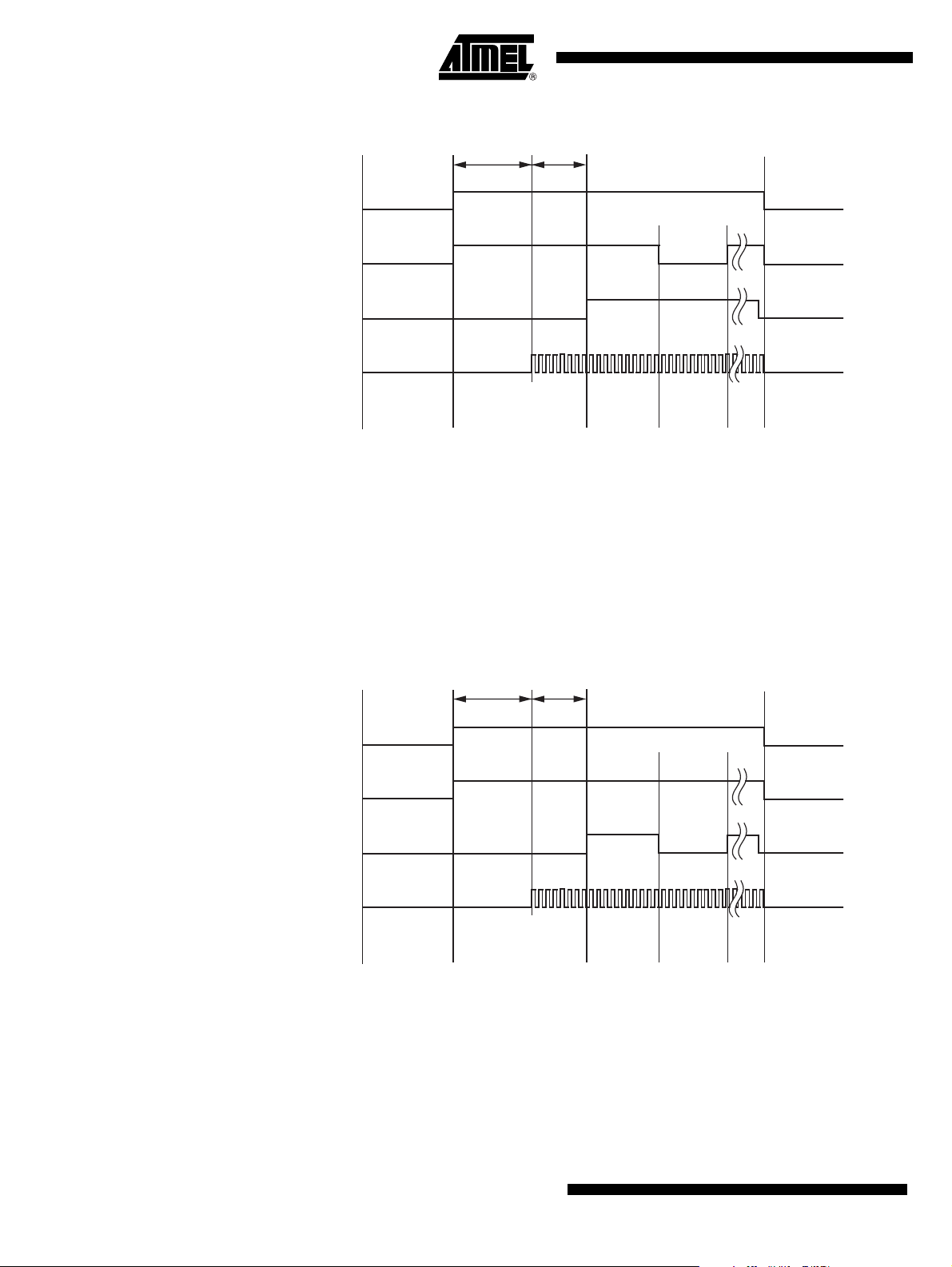
Figure 4-4. Timing FSK Mode with ENABLE Connected to the Microcontroller
4.5.2.2 ASK Mode
XTO
PA off
> 250 µs
Power-up,
PA on
(f
= High)
RF
Power-up,
PA off
(fRF = Low)
Power-downPower-down Power-up,
∆T
ENABLE
FSK
ASK
CLK
The ATA6285/ATA6286 is activated by ENABLE = High, FSK = High and ASK = Low. After activation the microcontroller is switched to external clocking. After typically 0.6 ms, the CLK driver
is activated automatically (the microcontroller waits until the XTO and CLK are ready). After
another time period of ≤250 µs, the PLL is locked and ready to transmit. The output power can
then be modulated by means of pin ASK. After transmission, ASK is switched to Low and the
microcontroller returns back to internal clocking. Then, the ATA6285/ATA6286 is switched to
power-down mode with ENABLE = Low and FSK = Low.
Figure 4-5. Timing ASK Mode with ENABLE Connected to the Microcontroller
XTO
PA off
> 250 µs
Power-up,
PA on
(High)
Power-up,
PA off
(Low)
Power-downPower-down Power-up,
∆T
ENABLE
FSK
ASK
CLK
14
ATA6285/ATA6286 [Preliminary]
4958AS–AUTO–09/06
Page 15
4.5.3 Accuracy of Frequency Deviation
The accuracy of the frequency deviation using the XTAL pulling method is about ±20% if the following tolerances are considered. One important aspect is that the values of C
typical crystals are strongly correlated which reduces the tolerance of the frequency deviation.
Figure 4-6. Tolerances of Frequency Modulation
ATA6285/ATA6286 [Preliminary]
and CM of
0
V
S
C
Stray
XTAL
Using a crystal with a motional capacitance of C
of CL
C
=297× CM (the correlation has a tolerance of 10%, so C0= 267 to 326 × CM). If using the
0
= 18 pF and a parallel capacitance of C0= 1.30 pF correlated with CM results in
NOM
internal FSK switch with C
the resulting C
and C5 values are C4= 10 pF ±1% and C5= 15 pF ±1% for a nominal frequency
4
deviation of ±19.3 kHz with worst case tolerances of ±15.8 kHz to ±23.2 kHz.
4.5.4 Accuracy of the Center Frequency
The imaginary part of the impedance in large signal steady state oscillation IM
pin 7 (XTO1), causes some additional frequency tolerances, due to pulling of the XTO oscillation
frequency. These tolerances have to be added to the tolerances of the crystal itself (adjustment
tolerance, temperature stability and ageing) and the influence to the center frequency due to tolerances of C
, C5, C
4
should be absorbed into the C4 and C5 values by using a crystal with known frequency and
choosing C
and C5, so that the XTO center frequency equals the crystal frequency, and the fre-
4
quency deviation is as expected. Then, from the nominal value, the IM
using the pulling formula P = –IM
additional frequency tolerance of P = ±16.86 ppm results. If using crystals with other C
additional frequency tolerance can be calculated in the same way. For example, a lower
C
= 3.1 fF will reduce the frequency tolerance to 11.87 ppm, where a higher CM= 5.5 fF
M
increases the tolerance to 21.07 ppm.
Switch
C
M
C
Crystal equivalent circuit
= 0.9 pF ±20% and estimated parasitics of C
Switch
and C
. The nominal value of IM
Stray
× CM× Pi × f
XTO
S
M
0
= 4.37 fF ±15%, a nominal load capacitance
M
XTO
with f
= 13.56 MHz and CM= 4.4 fF an
XTO
R
L
C
5
XTO
C
4
C
Switch
= 0.7 pF ±10%,
Stray
, seen into the
XTO
= 110Ω, C
XTO
Switch
has ±90Ω tolerances,
and C
M
Stray
the
4.5.5 CLK Output
4958AS–AUTO–09/06
An output CLK signal of 1.64 MHz (ATA6285 operating at 315 MHz) and 1.69 MHz (ATA6286
operating at 433.92 MHz) is provided for a connected microcontroller. The delivered signal is
CMOS-compatible with a High and Low time of >125 ns if the load capacitance is lower than
20 pF. The CLK output is Low in power-down mode due to an internal pull-down resistor. After
enabling the PLL and XTO the signal stays Low until the amplitude of the crystal oscillator has
reached 35% to 80% of its amplitude. Then, the CLK output is activated synchronously with its
output signal so that the first period of the CLK output signal is a full period.
15
Page 16

4.5.5.1 Clock Pulse Take-over by Microcontroller
The clock of the crystal oscillator can be used for clocking the microcontroller. Atmel’s ATARx9x
microcontroller family provides the special feature of starting with an integrated RC oscillator to
switch on the ATA6285/ATA6286 external clocking and to wait automatically until the CLK output of the ATA6285/ATA6286 is activated. After a time period of 250 µs the message can be
sent with crystal accuracy.
4.5.6 Output Matching and Power Setting
The output power is set by the load impedance of the antenna. The maximum output power is
achieved with a load impedance of Z
Z
Load, opt
=280Ω + j310Ω (ATA6285) at 433.92 MHz. A low resistive path to VS is required to
deliver the DC current.
The power amplifier delivers a current pulse and the maximum output power is delivered to a
resistive load if the 0.66 pF output capacitance of the power amplifier is compensated by the
load impedance.
Load, opt
= 380Ω + j340Ω (ATA6286) at 315 MHz and
At the ANT1 pin, the RF output amplitude is about V
– 0.5V.
S
The load impedance is defined as the impedance seen from the ATA6285’s ANT1, ANT2 into
the matching network. Do not mix up this large-signal load impedance with a small-signal input
impedance delivered as an input characteristic of RF amplifiers.
The latter is measured from the application into the IC instead of from the IC into the application
for a power amplifier.
The 0.66 pF output capacitance absorbed into the load impedance a real impedance of 684Ω
(ATA6285) at 315 MHz and 623Ω (ATA6286) at 433.92 MHz should be measured with a network
analyses at pin 5 (ANT1) with the ATA6285/ATA6286 soldered, an optimized antenna connected and the power amplifier switched off.
Less output power is achieved by lowering the real parallel part where the parallel imaginary part
should be kept constant. Lowering the real part of the load impedance also reduces the supply
voltage dependency of the output power.
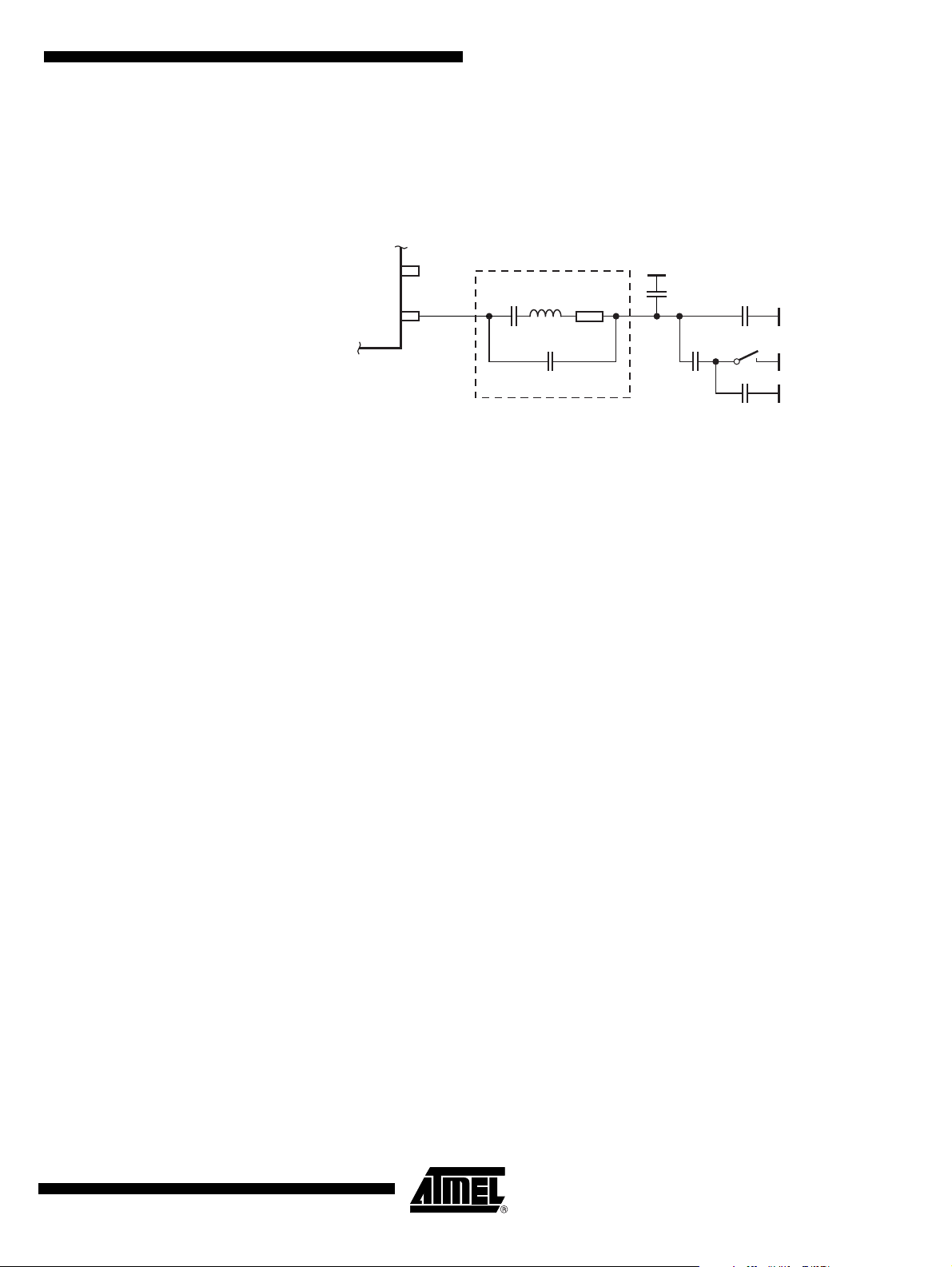
Output power measurement can be done with the circuit as shown in Output Power Measurement. Please note that the component values must be changed to compensate the individual
board parasitics until the ATA6285/ATA6286 has the right load impedance. Also, the damping of
the cable used to measure the output power must be calibrated.
Figure 4-7. Output Power Measurement ATA6285/ATA6286
V
S
16
C
= 1 nF
1
L1 = 68 nH/ 39 nH
ANT1
= 2.2 pF/ 1.8 pF
Lopt
C
2
Z
ANT2
ATA6285/ATA6286 [Preliminary]
Z = 50Ω
Power
meter
R
in
50Ω
4958AS–AUTO–09/06
Page 17

ATA6285/ATA6286 [Preliminary]
5. Ordering Information
Extended Type Number Package Frequency MOQ Remarks
ATA6285-PNPW QFN32 315 MHz Packaging unit: 1,500 Taped and reeled
ATA6286-PNPW QFN32 433 MHz Packaging unit: 1,500 Taped and reeled
ATA6285-PNQW QFN32 315 MHz 6,000 Taped and reeled
ATA6286-PNQW QFN32 433 MHz 6,000 Taped and reeled
6. Package Information
Package: QFN_ 5 x 5_32L
Exposed pad 3.6 x 3.6
Dimensions in mm
Not indicated tolerances ±0.05
Top
32
1
Pin1 identification
Bottom
3.6±0.15
25 32
24
1
17
Drawing-No.: 6.543-5124.01-4
Issue: 1; 28.11.05
17
16 9
5
0.2
0.9±0.1
Z
8
0.5 nom.
3.5
Z 10:1
0.4±0.1
technical drawings
according to DIN
specifications
0.23±0.07
4958AS–AUTO–09/06
17
Page 18

Atmel Corporation Atmel Operations
2325 Orchard Parkway
San Jose, CA 95131, USA
Tel: 1(408) 441-0311
Fax: 1(408) 487-2600
Regional Headquarters
Europe
Atmel Sarl
Route des Arsenaux 41
Case Postale 80
CH-1705 Fribourg
Switzerland
Tel: (41) 26-426-5555
Fax: (41) 26-426-5500
Asia
Room 1219
Chinachem Golden Plaza
77 Mody Road Tsimshatsui
East Kowloon
Hong Kong
Tel: (852) 2721-9778
Fax: (852) 2722-1369
Japan
9F, Tonetsu Shinkawa Bldg.
1-24-8 Shinkawa
Chuo-ku, Tokyo 104-0033
Japan
Tel: (81) 3-3523-3551
Fax: (81) 3-3523-7581
Memory
2325 Orchard Parkway
San Jose, CA 95131, USA
Tel: 1(408) 441-0311
Fax: 1(408) 436-4314
Microcontrollers
2325 Orchard Parkway
San Jose, CA 95131, USA
Tel: 1(408) 441-0311
Fax: 1(408) 436-4314
La Chantrerie
BP 70602
44306 Nantes Cedex 3, France
Tel: (33) 2-40-18-18-18
Fax: (33) 2-40-18-19-60
ASIC/ASSP/Smart Cards
Zone Industrielle
13106 Rousset Cedex, France
Tel: (33) 4-42-53-60-00
Fax: (33) 4-42-53-60-01
1150 East Cheyenne Mtn. Blvd.
Colorado Springs, CO 80906, USA
Tel: 1(719) 576-3300
Fax: 1(719) 540-1759
Scottish Enterprise Technology Park
Maxwell Building
East Kilbride G75 0QR, Scotland
Tel: (44) 1355-803-000
Fax: (44) 1355-242-743
RF/Automotive
Theresienstrasse 2
Postfach 3535
74025 Heilbronn, Germany
Tel: (49) 71-31-67-0
Fax: (49) 71-31-67-2340
1150 East Cheyenne Mtn. Blvd.
Colorado Springs, CO 80906, USA
Tel: 1(719) 576-3300
Fax: 1(719) 540-1759
Biometrics/Imaging/Hi-Rel MPU/
High-Speed Converters/RF Datacom
Avenue de Rochepleine
BP 123
38521 Saint-Egreve Cedex, France
Tel: (33) 4-76-58-30-00
Fax: (33) 4-76-58-34-80
Literature Requests
www.atmel.com/literature
Disclaimer: The information in this document is provided in connection with Atmel products. No license, express or implied, by estoppel or otherwise, to any
intellectual property right is granted by this document or in connection with the sale of Atmel products. EXCEPT AS SET FORTH IN ATMEL’S TERMS AND CONDI-
TIONS OF SALE LOCATED ON ATMEL’S WEB SITE, ATMEL ASSUMES NO LIABILITY WHATSOEVER AND DISCLAIMS ANY EXPRESS, IMPLIED OR STATUTORY
WARRANTY RELATING TO ITS PRODUCTS INCLUDING, BUT NOT LIMITED TO, THE IMPLIED WARRANTY OF MERCHANTABILITY, FITNESS FOR A PARTICULAR
PURPOSE, OR NON-INFRINGEMENT. IN NO EVENT SHALL ATMEL BE LIABLE FOR ANY DIRECT, INDIRECT, CONSEQUENTIAL, PUNITIVE, SPECIAL OR INCIDENTAL DAMAGES (INCLUDING, WITHOUT LIMITATION, DAMAGES FOR LOSS OF PROFITS, BUSINESS INTERRUPTION, OR LOSS OF INFORMATION) ARISING OUT
OF THE USE OR INABILITY TO USE THIS DOCUMENT, EVEN IF ATMEL HAS BEEN ADVISED OF THE POSSIBILITY OF SUCH DAMAGES. Atmel makes no
representations or warranties with respect to the accuracy or completeness of the contents of this document and reserves the right to make changes to specifications
and product descriptions at any time without notice. Atmel does not make any commitment to update the information contained herein. Unless specifically provided
otherwise, Atmel products are not suitable for, and shall not be used in, automotive applications. Atmel’s products are not intended, authorized, or warranted for use
as components in applications intended to support or sustain life.
© 2006 Atmel Corporation. All rights reserved. Atmel®, logo and combinations thereof, Everywhere You Are® and others are registered trade-
marks or trademarks of Atmel Corporation or its subsidiaries. Other terms and product names may be trademarks of others.
4958AS–AUTO–09/06
 Loading...