

Page 1

Features
• High FSK Sensitivity: -106 dBm at 20 kBaud/-109.5 dBm at 2.4 kBaud (433.92 MHz)
• High ASK Sensitivity: -112.5 dBm at 10 kBaud/-116.5 dBm at 2.4 kBaud (433.92 MHz)
• Low Supply Current: 10.5 mA in RX and TX Mode (3 V/TX with 5 dBm)
• Data Rate 1 to 20 kBaud Manchester FSK, 1 to 10 kBaud Manchester ASK
• ASK/FSK Receiver Uses a Low-IF Architecture with High Selectivity, Blocking and Low
Intermodulation (Typical Blocking 55
dB at ±10 MHz, System I1dBCP = -30 dBm/System IIP3 = -20 dBm)
70
• 226 kHz IF Frequency with 30 dB Image Rejection and 170 kHz Usable IF Bandwidth
• Transmitter Uses Closed Loop Fractional-N Synthesizer for FSK Modulation with a
High PLL Bandwidth and an Excellent Isolation between PLL and PA
• Tolerances of XTAL Compensated by Fractional-N Synthesizer with 800 Hz RF
Resolution
• Integrated RX/TX-Switch, Single-ended RF Input and Output
• RSSI (Received Signal Strength Indicator)
• Communication to Microcontroller with SPI Interface Working at Maximum 500 kBit/s
• Configurable Self Polling and RX/TX Protocol Handling with FIFO-RAM Buffering of
Received and Transmitted Data
• 5 Push Button Inputs and One Wake-up Input are Active in Power-down Mode
• Integrated XTAL Capacitors
• PA Efficiency: up to 38% (433 MHz/10 dBm/3 V)
• Low Inband Sensitivity Change of Typically ±1.8 dB within ±58 kHz Center Frequency
Change in the Complete Temperature and Supply Voltage Range
• Supply Voltage Switch, Supply Voltage Regulator, Reset Generation, Clock/Interrupt
Generation and Low Battery Indicator for Microcontroller
• Fully Integrated PLL with Low Phase Noise VCO and PLL Loop Filter
• Sophisticated Threshold Control and Quasi Peak Detector Circuit in the Data Slicer
• Power Management via Different Operation Modes
• 433.92 MHz, 868.3 MHz and 315 MHz without External VCO and PLL Components
• Inductive Supply with Voltage Regulator if Battery is Empty (AUX Mode)
• Efficient XTO Start-up Circuit (> -1.5 kΩ Worst Case Start Impedance)
• Changing of Modulation Type ASK/FSK and Data Rate without Component Changes
• Minimal External Circuitry Requirements for Complete System Solution
• Adjustable Output Power: 0 to 10 dBm Adjusted and Stabilized with External Resistor
• ESD Protection at all Pins (2 kV HBM, 200 V MM)
• Supply Voltage Range: 2.4 V to 3.6 V or 4.4 V to 6.6 V
• Temperature Range: -40°C to +105°C
• Small 7 × 7 mm QFN48 Package
dB at ±750 kHz/61 dB at ±1.5 MHz and
UHF ASK/FSK
Transceiver
ATA5811
ATA5812
Preliminary
Applications
• Automotive Keyless Entry and Passive Entry Go Systems
• Access Control Systems
• Remote Control Systems
• Alarm and Telemetry Systems
• Energy Metering
• Home Automation
Benefits
• No SAW Device Needed in Key Fob Designs to Meet Automotive Specifications
• Low System Cost Due to Very High System Integration Level
• Only One Crystal Needed in System
• Less Demanding Specification for the Microcontroller Due to Handling of Power-down
Mode, Delivering of Clock, Reset, Low Battery Indication and Complete Handling of
Receive/Transmit Protocol and Polling
• Single-ended Design with High Isolation of PLL/VCO from PA and the Power Supply
Allows a Loop Antenna in the Key Fob to Surround the Whole Application
Rev. 4689B–RKE–04/04
Page 2
General Description The ATA5811/ATA5812 is a highly integrated UHF ASK/FSK single-channel half-duplex
transceiver with low power consumption supplied in a small QFN48 package. The
receive part is built as a fully integrated low-IF receiver, whereas direct PLL modulation
with the fractional-N synthesizer is used for FSK transmission and switching of the
power amplifier for ASK transmission.
The device supports data rates of 1 kBaud to 20 kBaud (FSK) and 1 kBaud to 10 kBaud
(ASK) in Manchester, Bi-phase and other codes in transparent mode. The ATA5811 can
be used in the 433 MHz to 435 MHz and the 868 MHz to 870 MHz band, the ATA5812
in the 314 MHz to 316 MHz band. The very high system integration level results in few
numbers of external components needed.
Due to its blocking and selectivity performance, together with the additional 15 dB to
20 dB loss and the narrow bandwidth of a typical key fob loop antenna, a bulky blocking
SAW is not needed in the key fob or sensor application. Additionally, the building blocks
needed for a typical RKE and access control system on both sides, the base and the
mobile stations, are fully integrated.
Its digital control logic with self polling and protocol generation enables a fast challenge
response systems without using a high-performance microcontroller. Therefore, the
ATA5811/ATA5812 contains a FIFO buffer RAM and can compose and receive the
physical messages themselves. This provides more time for the microcontroller to carry
out other functions such as calculating crypto algorithms, composing the logical messages and controlling other devices. Due to that, a standard 4-/8-bit microcontroller
without special periphery and clocked with the CLK output of about 4.5 MHz is sufficient
to control the communication link. This is especially valid for passive entry and access
control systems, where within less than 100 ms several challenge response communications with arbitration of the communication partner have to be handled.
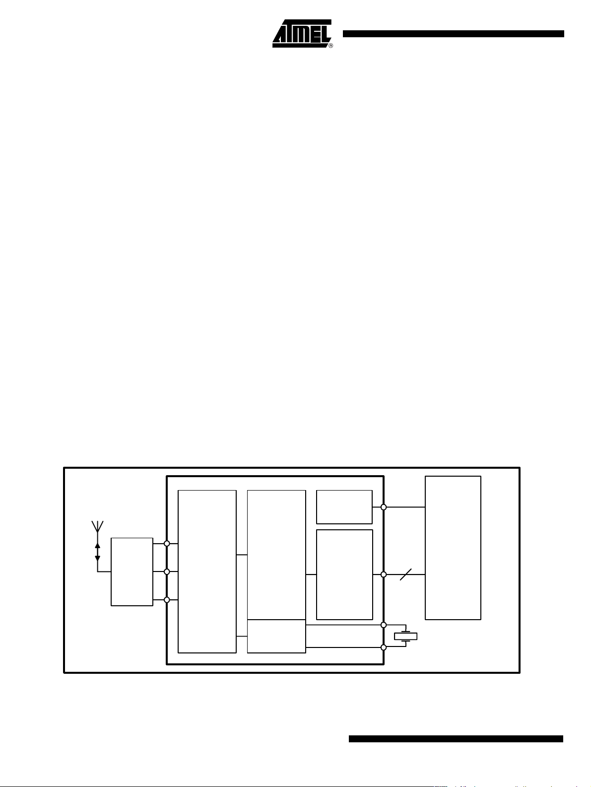
Figure 1. System Block Diagram
Antenna
Matching
It is hence possible to design bi-directional RKE and access control systems with a fast
challenge response crypto function with the same PCB board size and with the same
current consumption as uni-directional RKE systems.
ATA5811/ATA5812
RF transceiver
Digital Control
Logic
XTO
Power Supply
Micorcontroller
Interface
Microcontroller
4 ... 8
2
ATA5811/ATA5812 [Preliminary]
4689B–RKE–04/04
Page 3
Figure 2. Pinning QFN48
NC
NC
NC
RF_IN
NC
433_N868
NC
R_PWR
PWR_H
RF_OUT
NC
NC
ATA5811/ATA5812 [Preliminary]
NC
NC
RX_ACTIVET1T2T3T4T5PWR_ON
48 47 46 45 44 43 42 41 40 39 38 37
1
2
3
4
5
6
ATA5811/ATA5812
7
8
9
10
11
12
13 14 15 16 17 18 19 20 21 22 23 24
RX_TX1
RX_TX2
CDEM
36
RSSI
35
CS
34
DEM_OUT
33
SCK
32
SDI_TMDI
31
SDO_TMDO
30
CLK
29
IRQ
28
N_RESET
27
VSINT
26
NC
25
XTAL2
NCNCNC
VS2
VS1
AVCC
VAUX
DVCC
TEST1
VSOUT
XTAL1
TEST2
Pin Description
Pin Symbol Function
1 NC Not connected
2 NC Not connected
3 NC Not connected
4RF_INRF input
5 NC Not connected
6 433_N868 Selects RF input/output frequency range
7 NC Not connected
8 R_PWR Resistor to adjust output power
9 PWR_H Pin to select output power
10 RF_OUT RF output
11 NC Not connected
12 NC Not connected
13 NC Not connected
14 NC Not connected
15 NC Not connected
16 AVCC Blocking of the analog voltage supply
17 VS2 Power supply input for voltage range 4.4 V to 6.6 V
18 VS1 Power supply input for voltage range 2.4 V to 3.6 V
4689B–RKE–04/04
3
Page 4
Pin Description (Continued)
Pin Symbol Function
19 VAUX Auxiliary supply voltage input
20 TEST1 Test input, at GND during operation
21 DVCC Blocking of the digital voltage supply
22 VSOUT Output voltage power supply for external devices
23 TEST2 Test input, at GND during operation
24 XTAL1 Reference crystal
25 XTAL2 Reference crystal
26 NC Not connected
27 VSINT Microcontroller Interface supply voltage
28 N_RESET Output pin to reset a connected microcontroller
29 IRQ Interrupt request
30 CLK Output to clock a connected microcontroller
31 SDO_TMDO Serial data out/transparent mode data out
32 SDI_TMDI Serial data in/transparent mode data in
33 SCK Serial clock
34 DEM_OUT Demodulator open drain output signal
35 CS Chip select for serial interface
36 RSSI Output of the RSSI amplifier
37 CDEM Capacitor to adjust the lower cut-off frequency data filter
38 RX_TX2 GND pin to decouple LNA in TX mode
39 RX_TX1 Switch pin to decouple LNA in TX mode
40 PWR_ON Input to switch on the system (active high)
41 T1 Key input 1 (can also be used to switch on the system (active low)
42 T2 Key input 2 (can also be used to switch on the system (active low)
43 T3 Key input 3 (can also be used to switch on the system (active low)
44 T4 Key input 4 (can also be used to switch on the system (active low)
45 T5 Key input 5 (can also be used to switch on the system (active low)
46 RX_ACTIVE Indicates RX operation mode
47 NC Not connected
48 NC Not connected
GND Ground/backplane
4
ATA5811/ATA5812 [Preliminary]
4689B–RKE–04/04
Page 5
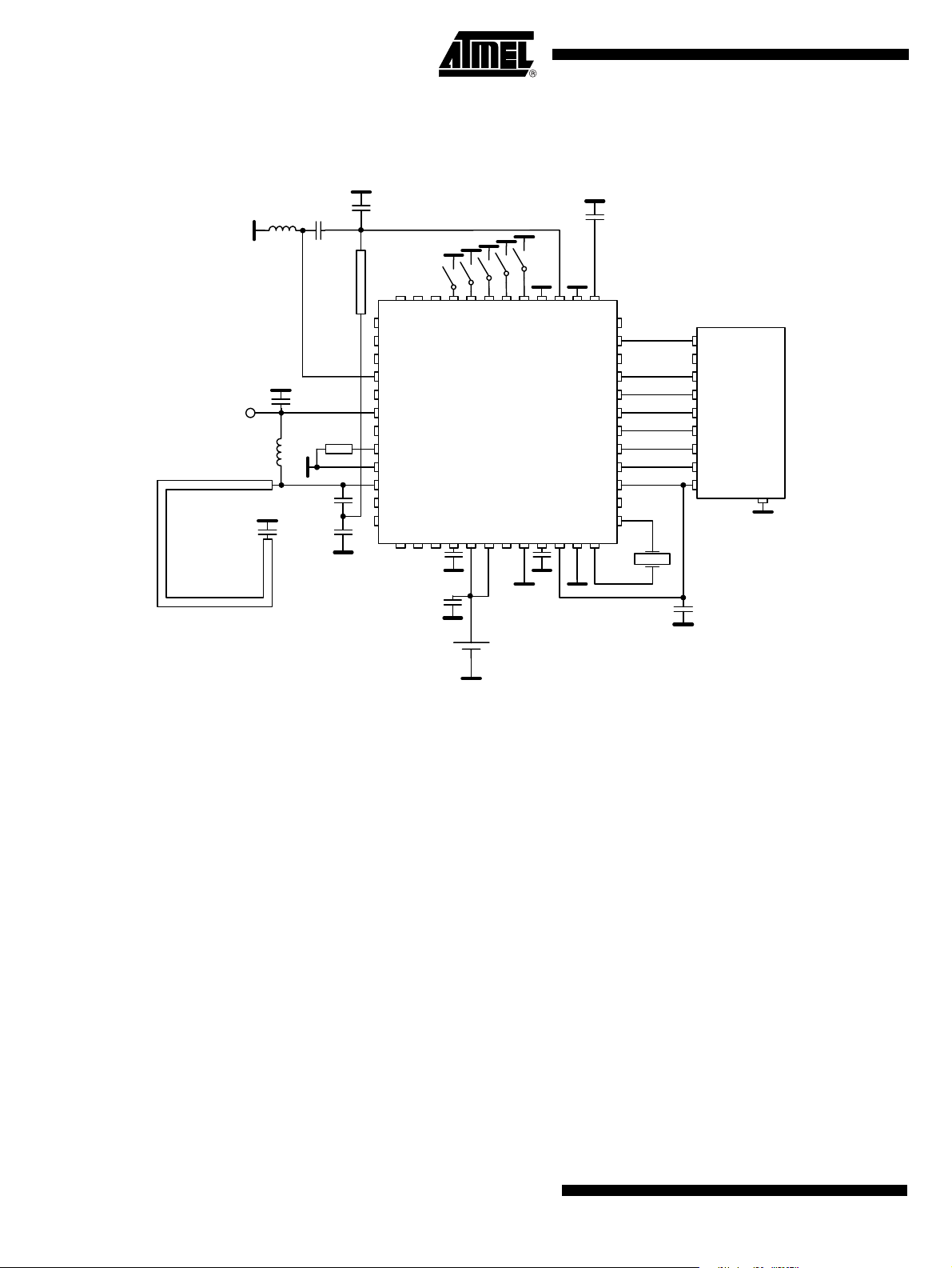
Figure 3. Block Diagram
ATA5811/ATA5812 [Preliminary]
433_N868
R_PWR
RF_OUT
PWR_H
RX_TX1
RX_TX2
RF_IN
CDEM
RSSI
XTAL1
XTAL2
DEM_OUT
CLK
N_RESET
IRQ
CS
SCK
SDI_TMDI
SDO_TMDO
AVCC
RF transceiver Digital Control Logic
PA
Fract.-N-
Frequency
TX
LNA
Microcontroller
Interface
Synthesizer
Signal
Processing
(Mixer, IF -
Filter, IF -
Amp.,
Demodulator,
Data Filter
Data Slicer)
Frontend Enable
PA_Enable (ASK)
TX_DATA (FSK)
RX/TX
FREQ 9
FREF
Demod_Out
RX_ACTIVE
TX/RX - Data Buffer
Control Register
Status Register
Bit-Check Logic
DVCC
Polling Circuit
XTO
SPI
Power
Supply
Switches
Regulators
Wakeup
Reset
Reset
VS2
VS1
VAUX
VSOUT
PWR_ON
T1
T2
T3
T4
T5
TEST1
TEST2
4689B–RKE–04/04
VSINT
GND
5
Page 6
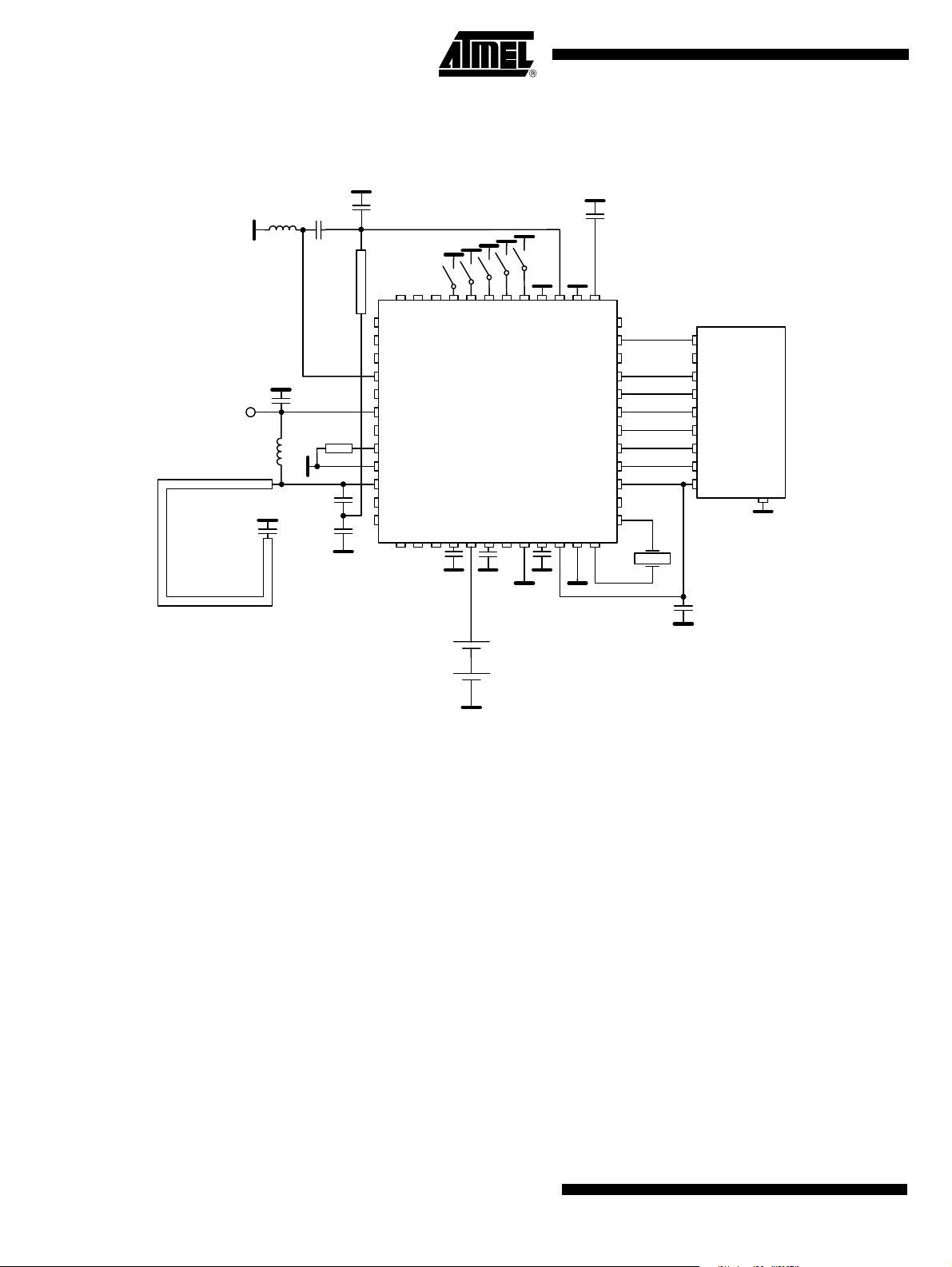
Typical Key Fob or Sensor Application with 1 Battery
Figure 4. Typical RKE Key Fob or Sensor Application, 433.92 MHz, 1 Battery
AVCC
C
10
Loop antenna
C
11
L
1
C
5
L
2
C
8
C
9
C
7
T2
T3
VS2
+
T4
VS1
VAUX
C
4
Litihum-
T5
TEST1
RX_TX1
PWR_ON
SDO_TMDO
DVCC
VSOUT
NC
NC
20 mm x 0.4 mm
NC
NC
RF_IN
NC
433_N868
NC
R
1
R_PWR
PWR_H
RF_OUT
NC
NC
NC
T1
NC
RX_ACTIVE
ATA5811/ATA5812
NC
NC
AVCC
C
1
C
2
CDEM
RSSI
RX_TX2
CS
DEM_OUT
SCK
SDI_TMDI
CLK
IRQ
N_RESET
VSINT
NC
TEST2
XTAL1
C
XTAL2
6
Microcontroller
VCC
VSS
13.25311 MHz
C
3
Cell
Figure 4 shows a typical 433.92 MHz RKE key fob or sensor application with one battery
The external components are 11 capacitors, 1 resistor, 2 inductors and a crystal. C
are 68 nF voltage supply blocking capacitors. C5 is a 10 nF supply blocking capaci-
C
4
is a 15 nF fixed capacitor used for the internal quasi peak detector and for the
tor. C
6
highpass frequency of the data filter. C
of 1 pF to 33 pF. L1 is a matching inductor of about 5.6 nH to 56 nH. L
tor of about 120 nH. A load capacitor of 9 pF for the crystal is integrated. R
to C11 are RF matching capacitors in the range
7
is a feed induc-
2
is typically
1
1
to
22 kΩ and sets the output power to about 5.5 dBm. The loop antenna’s quality factor is
somewhat reduced by this application due to the quality factor of L
and the RX/TX
2
switch. On the other hand, this lower quality factor is necessary to have a robust design
with a bandwidth that is broad enough for production tolerances. Due to the singleended and ground-referenced design, the loop antenna can be a free-form wire around
the application as it is usually employed in RKE uni-directional systems. The
ATA5811/ATA5812 provides sufficient isolation and robust pulling behavior of internal
circuits from the supply voltage as well as an integrated VCO inductor to allow this.
Since the efficiency of a loop antenna is proportional to the square of the surrounded
area it is beneficial to have a large loop around the application board with a lower quality
factor to relax the tolerance specification of the RF components and to get a high
antenna efficiency in spite of their lower quality factor.
6
ATA5811/ATA5812 [Preliminary]
4689B–RKE–04/04
Page 7
ATA5811/ATA5812 [Preliminary]
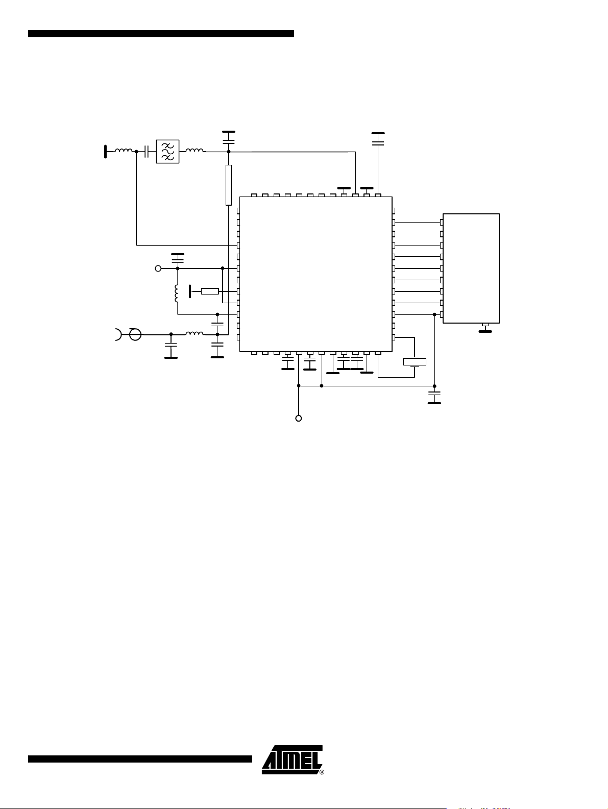
Typical Car or Sensor Base-station Application
Figure 5. Typical RKE Car or Sensor Base-station Application, 433.92 MHz
SAW-Filter
L
4
C
50 Ω
connector
RF
OUT
11
AVCC
C
10
L
3
C
5
R
L
2
C
L
8
1
C
9
C
7
NC
NC
T1
NC
20 mm x 0.4 mm
NC
NC
RF_IN
NC
433_N868
NC
1
R_PWR
PWR_H
RF_OUT
NC
NC
NC
NC
T2T3T4
RX_ACTIVE
ATA5811/ATA5812
AVCC
VS2
NC
VS1
T5
RX_TX1
PWR_ON
SDO_TMDO
VAUX
DVCC
TEST1
VSOUT
CDEM
RSSI
RX_TX2
CS
DEM_OUT
SCK
SDI_TMDI
CLK
IRQ
N_RESET
VSINT
NC
TEST2
XTAL1
C
6
XTAL2
Microcontroller
VCC
VSS
13.25311 MHz
C
C
1
C
2
C
4
12
C
3
VCC = 4.75 V..5.25 V
Figure 5 shows a typical 433.92 MHz VCC = 4.75 V to 5.25 V RKE car or sensor basestation application. The external components are 12 capacitors, 1 resistor, 4 inductors, a
SAW filter and a crystal. C
and C12 are 2.2 µF supply blocking capacitors for the internal voltage regulators. C
C
2
and C3 to C4 are 68 nF voltage supply blocking capacitors.
1
is a 10 nF supply blocking capacitor. C6 is a 15 nF fixed capacitor used for the internal
quasi peak detector and for the highpass frequency of the data filter. C
matching capacitors in the range of 1 pF to 33 pF. L
to L4 are matching inductors of
2
about 5.6 nH to 56 nH. A load capacitor for the crystal of 9 pF is integrated. R
to C11 are RF
7
is typi-
1
cally 22 kΩ and sets the output power at RF_OUT to about 10 dBm. Since a quarter
wave or PCB antenna, which has high efficiency and wide band operation, is typically
used here, it is recommended to use a SAW filter to achieve high sensitivity in case of
powerful out-of-band blockers. L
, C10 and C9 together form a lowpass filter, which is
1
needed to filter out the harmonics in the transmitted signal to meet regulations. An internally regulated voltage at pin VSOUT can be used in case the microcontroller only
supports 3.3
V operation, a blocking capacitor with a value of C
= 2.2 µF has to be
12
connected to VSOUT in any case.
5
4689B–RKE–04/04
7
Page 8
Typical Key Fob Application, 2 Batteries
Figure 6. Typical RKE Key Fob Application, 433.92 MHz, 2 Batteries
AVCC
C
Loop antenna
C
11
L
1
C
5
L
2
C
8
10
C
9
C
7
T2
T3T4T5
NC
NC
NC
20 mm x 0.4 mm
NC
RF_IN
NC
433_N868
R
NC
1
R_PWR
PWR_H
RF_OUT
NC
NC
NC
T1
NC
RX_ACTIVE
ATA5811/ATA5812
NC
AVCC
NC
C
VS2
1
C
VS1
2
PWR_ON
SDO_TMDO
VAUX
DVCC
TEST1
C
4
CDEM
RSSI
RX_TX1
RX_TX2
DEM_OUT
SDI_TMDI
N_RESET
VSINT
TEST2
VSOUT
CS
SCK
CLK
IRQ
NC
XTAL1
C
6
XTAL2
Microcontroller
VCC
VSS
13.25311 MHz
C
3
+
Litihum Cells
+
Figure 6 shows a typical 433.92 MHz 2-battery RKE key fob or sensor application. The
external components are 11 capacitors, 1 resistor, 2 inductors and a crystal. C
and C
1
4
are 68 nF voltage supply blocking capacitors. C2 and C3 are 2.2 µF supply blocking
capacitors for the internal voltage regulators. C
is a 10 nF supply blocking capacitor. C
5
6
is a 15 nF fixed capacitor used for the internal quasi peak detector and for the highpass
frequency of the data filter. C
33 pF. L
is a matching inductor of about 5.6 nH to 56 nH. L2 is a feed inductor of about
1
120 nH. A load capacitor for the crystal of 9 pF is integrated. R
to C11 are RF matching capacitors in the range of 1 pF to
7
is typically 22 kΩ and
1
sets the output power to about 5.5 dBm.
8
ATA5811/ATA5812 [Preliminary]
4689B–RKE–04/04
Page 9

ATA5811/ATA5812 [Preliminary]
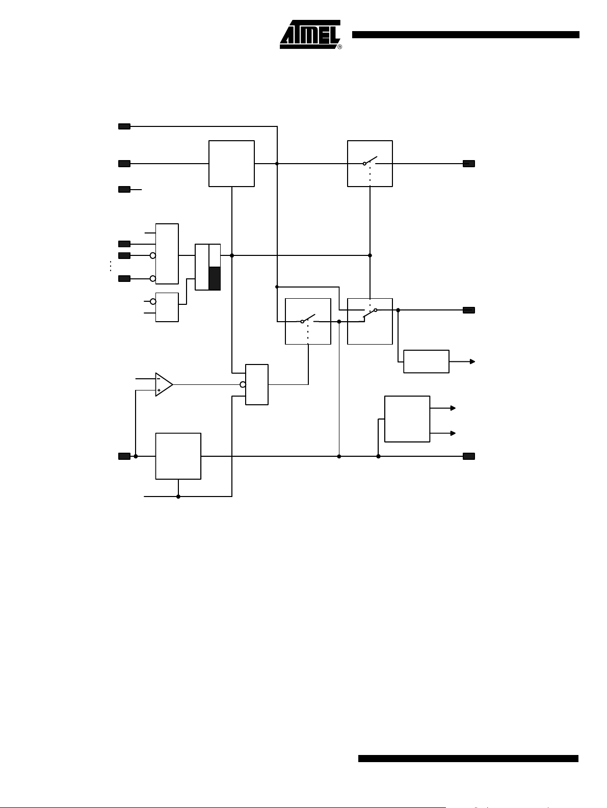
RF Transceiver According to Figure 3 on page 5, the RF transceiver consists of an LNA (Low-Noise
Amplifier), PA (Power Amplifier), RX/TX switch, fractional-N frequency synthesizer and
the signal processing part with mixer, IF filter, IF amplifier, FSK/ASK demodulator, data
filter and data slicer.
In receive mode the LNA pre-amplifies the received signal which is converted down to
226 kHz, filtered and amplified before it is fed into an FSK/ASK demodulator, data filter
and data slicer. The RSSI (Received Signal Strength Indicator) signal and the raw digital
output signal of the demodulator are available at the pins RSSI and DEM_OUT. The
demodulated data signal Demod_Out is fed to the digital control logic where it is evaluated and buffered as described in section “Digital Control Logic”.
In transmit mode the fractional-N frequency synthesizer generates the TX frequency
which is fed to the PA. In ASK mode the PA is modulated by the signal PA_Enable. In
FSK mode the PA is enabled and the signal TX_DATA (FSK) modulates the fractional-N
frequency synthesizer. The frequency deviation is digitally controlled and internally fixed
to about ±16 kHz (see Table 12 on page 24 for exact values). The transmit data can
also be buffered as described in section “Digital Control Logic”. A lock detector within
the synthesizer ensures that the transmission will only start if the synthesizer is locked.
The RX/TX switch can be used to combine the LNA input and the PA output to a single
antenna with a minimum of losses.
Transparent modes without buffering of RX and TX data are also available to allow protocols and coding schemes other than the internal supported Manchester encoding.
Low-IF Receiver The receive path consists of a fully integrated low-IF receiver. It fulfills the sensitivity,
blocking, selectivity, supply voltage and supply current specification needed to manufacture an automotive key fob without the use of SAW blocking filter (see Figure 4 on
page 6). The receiver can be connected to the roof antenna in the car when using an
additional blocking SAW front-end filter as shown in Figure 5 on page 7.
At 433.92 MHz the receiver has a typical system noise figure of 7.0 dB, a system
I1dBCP of -30 dBm and a system IIP3 of -20 dBm. There is no AGC or switching of the
LNA needed, thus, a better blocking performance is achieved. This receiver uses an IF
(Intermediate Frequency) of 226 kHz, the typical image rejection is 30 dB and the typical
3 dB IF filter bandwidth is 185 kHz (f
= 318.5 kHz). The demodulator needs a signal to Gaussian noise ratio of 8 dB for
f
hi_IF
= 226 kHz ±92.5 kHz, f
IF
20 kBaud Manchester with ±16 kHz frequency deviation in FSK mode, thus, the resulting sensitivity at 433.92 MHz is typically -106 dBm at 20 kBaud Manchester.
Due to the low phase noise and spurious of the synthesizer in receive mode
with the eighth order integrated IF filter the receiver has a better selectivity and blocking
performance than more complex double superhet receivers but without external components and without numerous spurious receiving frequencies.
A low-IF architecture is also less sensitive to second-order intermodulation (IIP2) than
direct conversion receivers where every pulse or AM-modulated signal (especially the
signals from TDMA systems like GSM) demodulates to the receiving signal band at second-order non-linearities.
Note: 1. -120 dBC/Hz at ±1 MHz and -75 dBC at ±FREF at 433.92 MHz
= 133.5 kHz and
lo_IF
(1)
together
4689B–RKE–04/04
9
Page 10
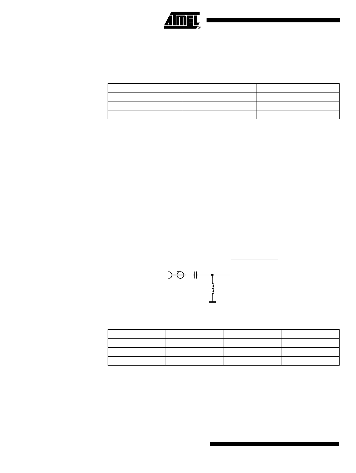
Input Matching at RF_IN The measured input impedances as well as the values of a parallel equivalent circuit of
these impedances can be seen in Table 1. The highest sensitivity is achieved with
power matching of these impedances to the source impedance of 50 Ω
Table 1. Measured Input Impedances of the RF_IN Pin
fRF/MHz Z(RF_IN) Rp//C
315 (44-j233)Ω 1278 Ω//2.1 pF
433.92 (32-j169)Ω 925 Ω//2.1 pF
868.3 (21-j78)Ω 311 Ω//2.2 pF
The matching of the LNA Input to 50 Ω was done with the circuit according to Figure 7
and with the values given in Table 2. The reflection coefficients were always ≤ 10 dB.
Note that value changes of C
board layouts. The measured typical FSK and ASK Manchester code sensitivities with a
Bit Error Rate (BER) of 10
and L1 may be necessary to for compensate individual
1
-3
are shown in Table 3 on page 11 and Table 4 on page 11.
These measurements were done with inductors having a quality factor according to
Table 2, resulting in estimated matching losses of 1.0 dB at 315 MHz, 1.2 dB at
433.92 MHz and 0.6 dB at 868.3 MHz. These losses can be estimated when calculating
the parallel equivalent resistance of the inductor with R
matching loss with 10 log(1+R
p/Rloss
).
= 2 × π × f × L × QL and the
loss
With an ideal inductor, for example, the sensitivity at 433.92 MHz/FSK/20 kBaud/
±16 kHz/Manchester can be improved from -106 dBm to -107.2 dBm. The sensitivity
depends on the control logic which examines the incoming data stream. The examination limits must be programmed in control registers 5 and 6. The measurements in
Table 3 on page 11 and Table 4 on page 11 are based on the values of registers 5 and
6 according to Table 39 on page 57.
p
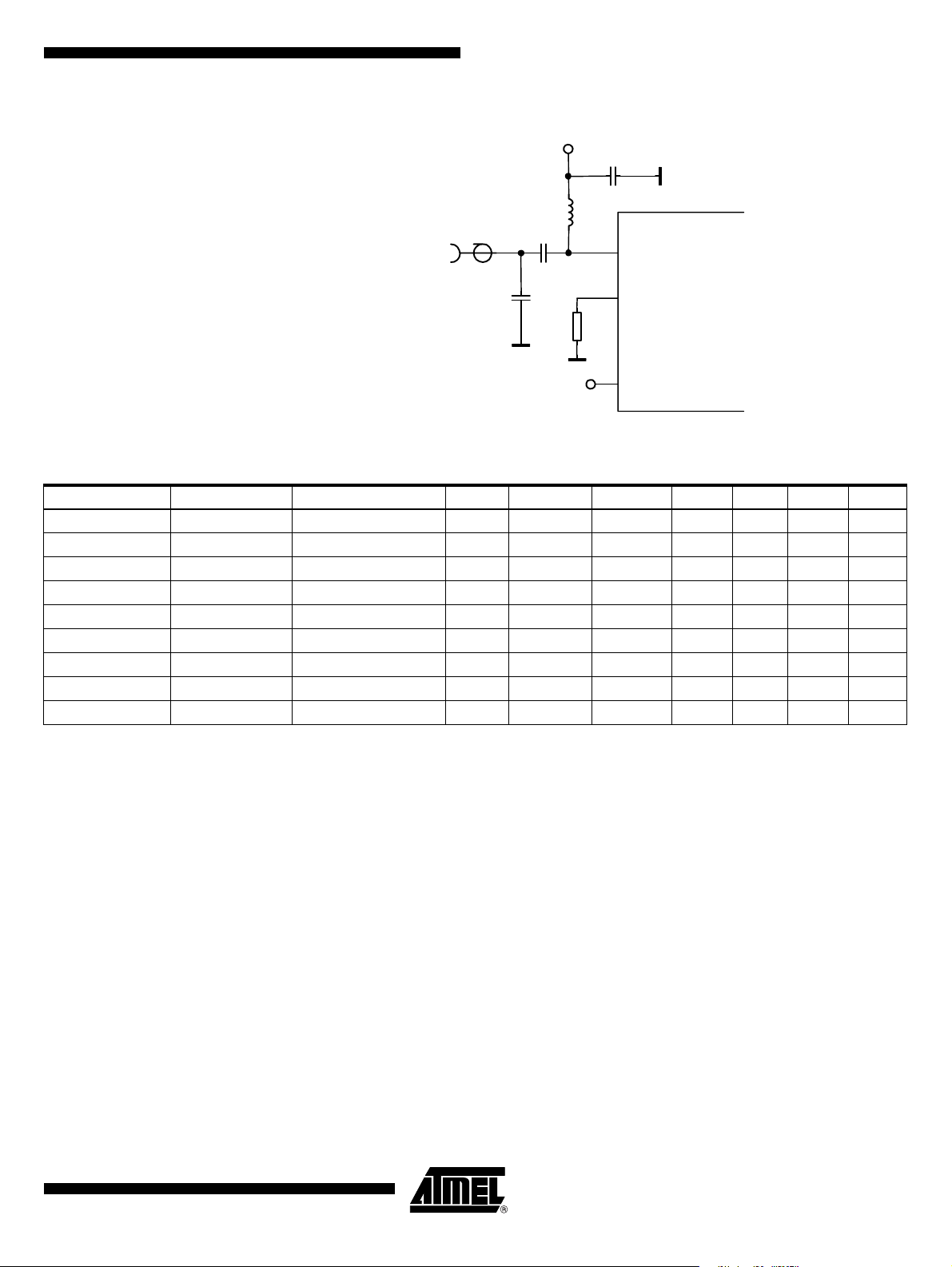
Figure 7. Input Matching to 50 Ω
RF
IN
Table 2. Input Matching to 50 Ω
fRF/MHz C1/pF L1/nH Q
315 2.2 56 43
433.92 1.8 27 40
868.3 1.2 6.8 58
C
1
ATA5811/ATA5812
4
RF_IN
L
1
L1
10
ATA5811/ATA5812 [Preliminary]
4689B–RKE–04/04
Page 11
ATA5811/ATA5812 [Preliminary]
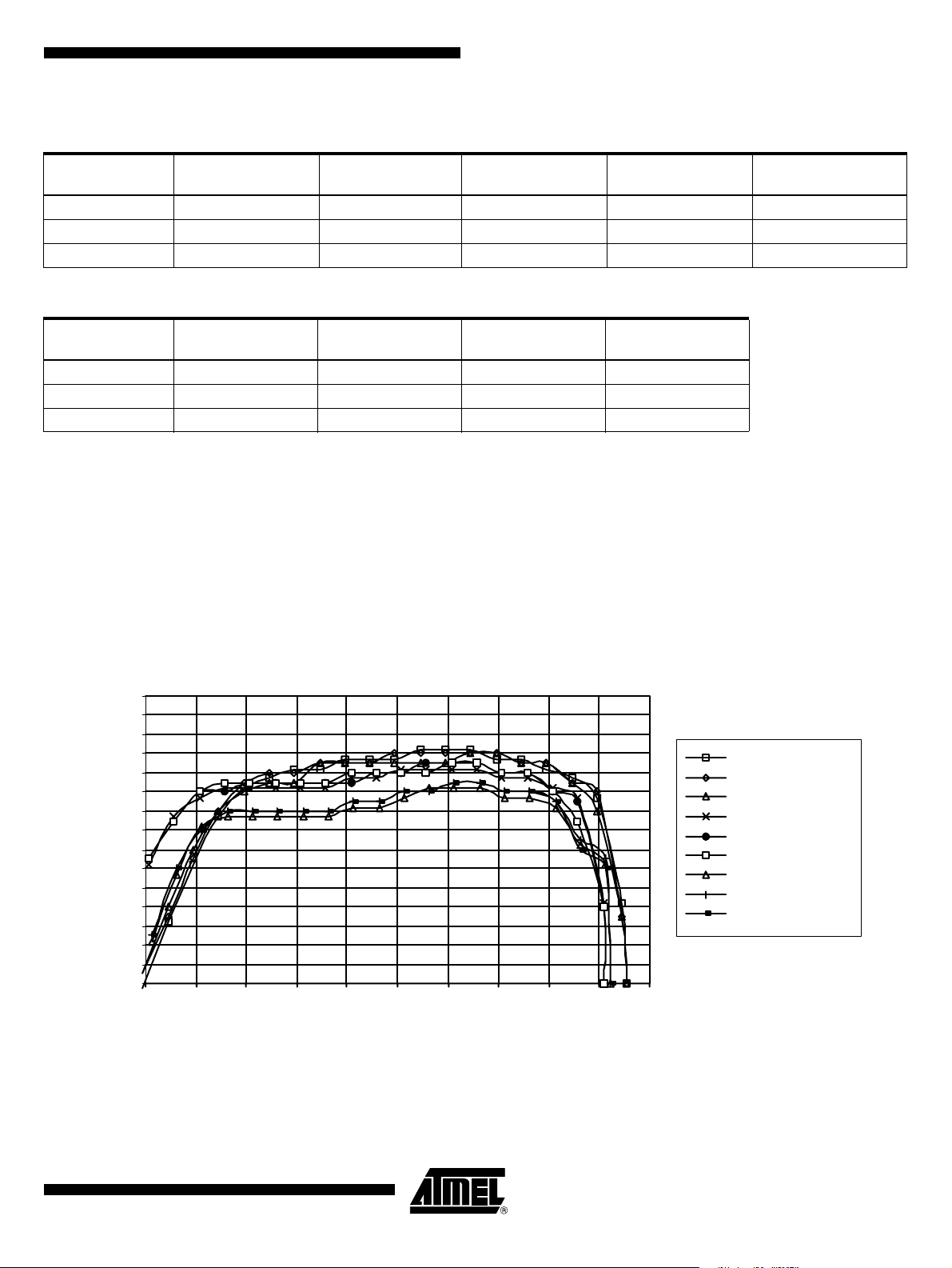
Table 3. Measured Sensitivity FSK, ±16 kHz, Manchester, dBm, BER = 10
RF Frequency
BR_Range_0
1.0 kBaud
BR_Range_0
2.4 kBaud
BR_Range_1
5.0 kBaud
-3
BR_Range_2
10 kBaud
BR_Range_3
20 kBaud
315 MHz -110.0 dBm -110.5 dBm -109.0 dBm -108.0 dBm -107.0 dBm
433.92 MHz -109.0 dBm -109.5 dBm -108.0 dBm -107.0 dBm -106.0 dBm
868.3 MHz -106.0 dBm -106.5 dBm -105.5 dBm -104.0 dBm -103.5 dBm
Table 4. Measured Sensitivity 100% ASK, Manchester, dBm, BER = 10
RF Frequency
BR_Range_0
1.0 kBaud
BR_Range_0
2.4 kBaud
BR_Range_1
5.0 kBaud
-3
BR_Range_2
10 kBaud
315 MHz -117.0 dBm -117.5 dBm -115 dBm -113.5 dBm
433.92 MHz -116.0 dBm -116.5 dBm -114.0 dBm -112.5 dBm
868.3 MHz -112.5 dBm -113.0 dBm -111.5 dBm -109.5 dBm
Sensitivity versus Supply Voltage, Temperature and Frequency Offset
To calculate the behavior of a transmission system it is important to know the reduction
of the sensitivity due to several influences. The most important are frequency offset due
to crystal oscillator (XTO) and crystal frequency (XTAL) errors, temperature and supply
voltage dependency of the noise figure and IF filter bandwidth of the receiver. Figure 8
shows the typical sensitivity at 433.92 MHz/FSK/20kBaud/±16 kHz/Manchester versus
the frequency offset between transmitter and receiver with T
= -40°C, +25°C and
amb
+105°C and supply voltage VS1 = VS2 = 2.4 V, 3.0 V and 3.6 V.
Figure 8. Measured Sensitivity 433.92 MHz/FSK/20 kBaud/±16 kHz/Manchester versus Frequency Offset, Temperature
and Supply Voltage
-110.0
-109.0
-108.0
-107.0
-106.0
-105.0
-104.0
-103.0
-102.0
-101.0
Sensitivity (dBm)
-100.0
-99.0
-98.0
-97.0
-96.0
-95.0
-100 -80 -60 -40 -20 0 20 40 60 80 100
Frequency Offset (kHz)
VS = 2.4 V T
VS = 3.0 V T
VS = 3.6 V T
VS = 2.4 V T
VS = 3.0 V T
VS = 3.6 V T
VS = 2.4 V T
VS = 3.0 V T
VS = 3.6 V T
= -40°C
amb
= -40°C
amb
= -40°C
amb
= +25°C
amb
= +25°C
amb
= +25°C
amb
= +105°C
amb
= +105°C
amb
= +105°C
amb
4689B–RKE–04/04
11
Page 12

As can be seen in Figure 8 on page 11 the supply voltage has almost no influence. The
temperature has an influence of about +1.5/-0.7 dB and a frequency offset of ±65 kHz
also influences by about ±1 dB. All these influences, combined with the sensitivity of a
typical IC, are then within a range of -103.7 dBm and -107.3 dBm over temperature,
supply voltage and frequency offset which is -105.5 dBm ±1.8dB. The integrated IF filter
has an additional production tolerance of only ±7 kHz, hence, a frequency offset
between the receiver and the transmitter of ±58 kHz can be accepted for XTAL and XTO
tolerances.
Note: For the demodulator used in the ATA5811/ATA5812, the tolerable frequency offset does
not change with the data frequency, hence, the value of ±58 kHz is valid for up to
1 kBaud.
This small sensitivity spread over supply voltage, frequency offset and temperature is
very unusual in such a receiver. It is achieved by an internal, very fast and automatic frequency correction in the FSK demodulator after the IF filter, which leads to a higher
system margin. This frequency correction tracks the input frequency very quickly, if however, the input frequency makes a larger step (e.g., if the system changes between
different communication partners), the receiver has to be restarted. This can be done by
switching back to Idle mode and then again to RX mode. For that purpose, an automatic
mode is also available. This automatic mote switches to Idle mode and back into RX
mode every time a bit error occurs (see section “Digital Control Logic”).
Frequency Accuracy of the Crystals
RX Supply Current versus Temperature and Supply Voltage
The XTO is an amplitude regulated Pierce oscillator with integrated load capacitors. The
initial tolerances (due to the frequency tolerance of the XTAL, the integrated capacitors
on XTAL1, XTAL2 and the XTO’s initial transconductance gm) can be compensated to a
value within ±0.5 ppm by measuring the CLK output frequency and programming the
control registers 2 and 3 (see Table 20 on page 35 and Table 23 on page 36). The XTO
then has a remaining influence of less than ±2 ppm over temperature and supply voltage due to the bandgap controlled gm of the XTO.
The needed frequency stability of the used crystals over temperature and aging is hence
±58 kHz/433.92 MHz - 2 × ±2.5 ppm = ±128.66 ppm for 433.92 MHz and
±58 kHz/868.3 MHz - 2 × ±2.5 ppm = ±61.8 ppm for 868.3 MHz. Thus, the used crys-
tals in receiver and transmitter each need to be better than ±64.33 ppm for 433.92 MHz
and ±30.9 ppm for 868.3 MHz. In access control systems it may be advantageous to
have a more tight tolerance at the base-station in order to relax the requirement for the
key fob.
Table 5 shows the typical supply current at 433.92 MHz of the transceiver in RX mode
versus supply voltage and temperature with VS = VS1 = VS2. As you can see the supply current at 2.4 V and -40°C is less than the typical one which helps because this is
also the operation point where a lithium cell has the worst performance. The typical supply current at 315 MHz or 868.3 MHz in RX mode is about the same as for 433.92 MHz.
Table 5. Measured 433.92 MHz Receive Supply Current in FSK Mode
VS = 2.4 V 3.0 V 3.6 V
T
= -40°C 8.4 mA 8.8 mA 9.2 mA
amb
T
= 25°C 9.9 mA 10.3 mA 10.8 mA
amb
T
= 105°C 11.4 mA 11.9 mA 12.4 mA
amb
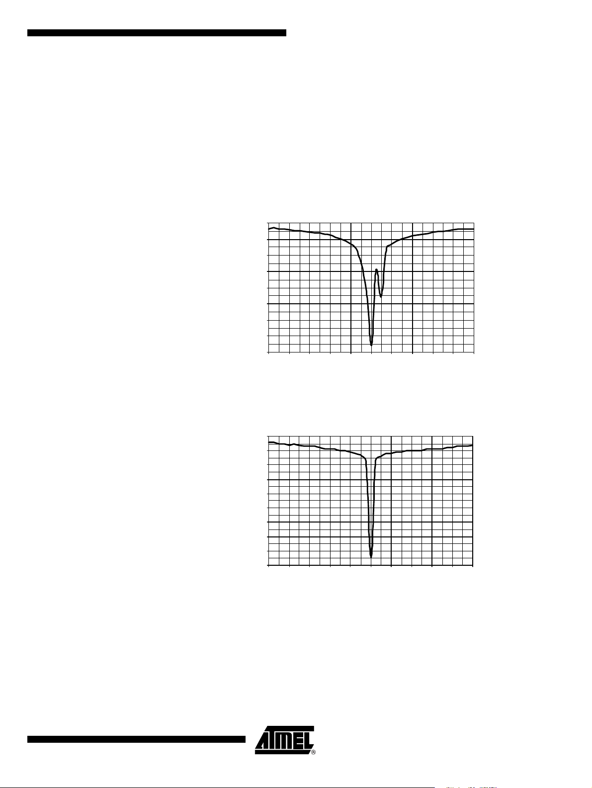
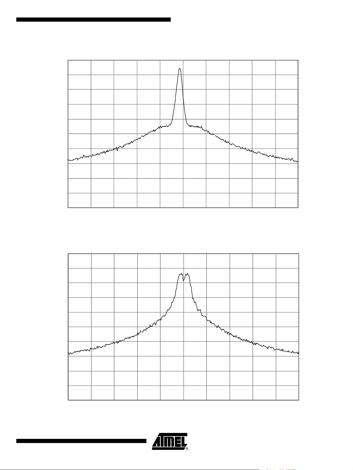
Blocking, Selectivity As can be seen in Figure 9 on page 13 and Figure 10 on page 13, the receiver can
receive signals 3 dB higher than the sensitivity level in presence of very large blockers
of -47 dBm/-34 dBm with small frequency offsets of ±1/±10 MHz.
12
ATA5811/ATA5812 [Preliminary]
4689B–RKE–04/04
Page 13
ATA5811/ATA5812 [Preliminary]
Figure 9 shows narrow band blocking and Figure 10 wide band blocking characteristics.
The measurements were done with a useful signal of 433.92 MHz/FSK/
kBaud/±16 kHz/Manchester with a level of -106 dBm + 3 dB = -103 dBm which is
20
dB above the sensitivity level. The figures show how much a continuous wave signal
3
can be larger than -103
done at the 50
Ω input according to Figure 7 on page 10. At 1 MHz, for example, the
blocker can be 56 dB higher than -103 dBm which is -103 dBm + 56 dB = -47 dBm.
These values, together with the good intermodulation performance, avoid the need for a
SAW filter in the key fob application.
Figure 9. Narrow Band 3 dB Blocking Characteristic at 433.92 MHz
70,0
60,0
50,0
40,0
30,0
20,0
Blocking Level [dBC]
-10,0
dBm until the BER is higher than 10-3. The measurements were
10,0
0,0
-5,0 -4,0 -3,0 -2,0 -1,0 0,0 1,0 2,0 3,0 4,0 5,0
Distance of Interfering to Receiving Signal [MHz]
Figure 10. Wide Band 3 dB Blocking Characteristic at 433.92 MHz
80,0
70,0
60,0
50,0
40,0
30,0
20,0
10,0
Blocking Level [dBC]
0,0
-10,0
-50,0 -40,0 -30,0 -20,0 -10,0 0,0 10,0 20,0 30,0 40,0 50,0
Distance of Interfering to Receiving Signal [MHz]
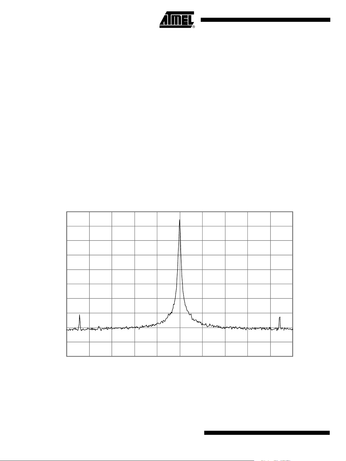
Figure 11 on page 14 shows the blocking measurement close to the received frequency
to illustrate the selectivity and image rejection. This measurement was done 6 dB above
the sensitivity level with a useful signal of 433.92 MHz/FSK/20kBaud/±16 kHz/
Manchester with a level of -106 dBm + 6 dB = -100 dBm. The figure shows to which
extent a continuous wave signal can surpass -100 dBm until the BER is higher than
-3
. For example, at 1 MHz the blocker can than be 59 dB higher than -100 dBm which
10
is -100 dBm + 59 dB = -41 dBm.
4689B–RKE–04/04
13
Page 14
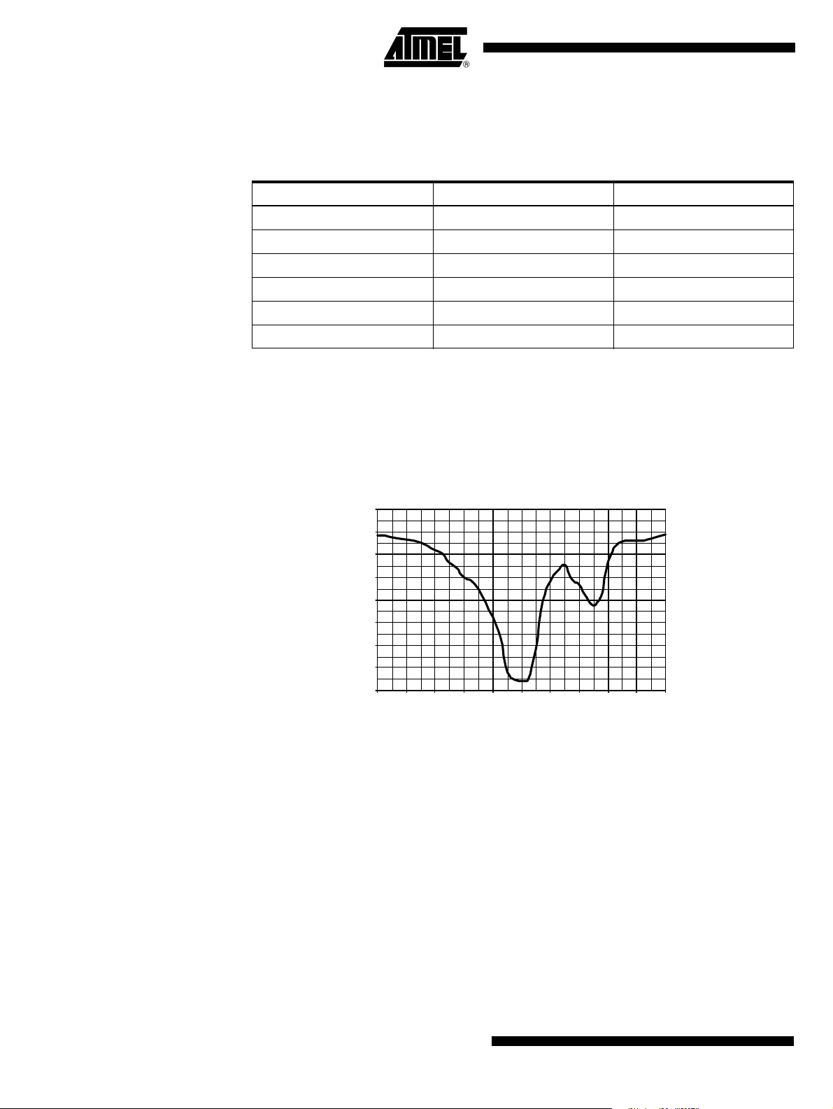
Table 6 shows the blocking performance measured relative to -100 dBm for some other
frequencies. Note that sometimes the blocking is measured relative to the sensitivity
level (dBS) instead of the carrier (dBC).
Table 6. Blocking 6 dB Above Sensitivity Level with BER < 10
Frequency Offset Blocker Level Blocking
+0.75 MHz -45 dBm 55 dBC/61 dBS
-0.75 MHz -45 dBm 55 dBC/61 dBS
+1.5 MHz -38 dBm 62 dBC/68 dBS
-1.5 MHz -38 dBm 62 dBC/68 dBS
+10 MHz -30 dBm 70 dBC/76 dBS
-10 MHz -30 dBm 70 dBC/76 dBS
-3
The ATA5811/ATA5812 can also receive FSK and ASK modulated signals if they are
much higher than the I1dBCP. It can typically receive useful signals at 10 dBm. This is
often referred to as the nonlinear dynamic range which is the maximum to minimum
receiving signal which is 116 dB for 20 kBaud Manchester. This value is useful if two
transceivers have to communicate and are very close to each other.
Figure 11. Close In 6 dB Blocking Characteristic and Image Response at 433.92 MHz
70.0
60.0
50.0
40.0
30.0
20.0
10.0
Blocking Level [dBC]
0.0
-10.0
-1.0 -0.8 -0.6 -0.4 -0.2 0.0 0.2 0.4 0.6 0.8 1.0
Distance of Interfering to Receiving Signal [MHz]
Inband Disturbers, Data Filter, Quasi Peak Detector, Data Slicer
14
ATA5811/ATA5812 [Preliminary]
This high blocking performance makes it even possible for some applications using
quarter wave whip antennas to use a simple LC band-pass filter instead of a SAW filter
in the receiver. When designing such an LC filter take into account that the 3 dB blocking at 433.92 MHz/2 = 216.96 MHz is 43 dBC and at 433.92 MHz/3 = 144.64 MHz is
48 dBC and at 2 × (433.92 MHz + 226 kHz) + -226 kHz = 868.066 MHz/868.518 MHz is
56 dBC. And especially that at 3 × (433.92 MHz + 226 kHz)+226 kHz = 1302.664 MHz
the receiver has its second LO harmonic receiving frequency with only 12 dBC blocking.
If a disturbing signal falls into the received band or a blocker is not continuous wave the
performance of a receiver strongly depends on the circuits after the IF filter. Hence the
demodulator, data filter and data slicer are important in that case.
4689B–RKE–04/04
Page 15
ATA5811/ATA5812 [Preliminary]
The data filter of the ATA5811/ATA5812 implies a quasi peak detector. This results in a
good suppression of the above mentioned disturbers and exhibits a good carrier to
Gaussian noise performance. The required useful signal to disturbing signal ratio to be
received with a BER of 10
(BR_Range_0 ... BR_Range_2)/6 dB (BR_Range_3) in FSK mode. Due to the many different waveforms possible these numbers are measured for signal as well as for
disturbers with peak amplitude values. Note that these values are worst case values and
are valid for any type of modulation and modulating frequency of the disturbing signal as
well as the receiving signal. For many combinations, lower carrier to disturbing signal
ratios are needed.
DEM_OUT Output The internal raw output signal of the demodulator Demod_Out is available at pin
DEM_OUT. DEM_OUT is an open drain output and must be connected to a pull-up
resistor if it is used (typically 100 kΩ) otherwise no signal is present at that pin.
RSSI Output The output voltage of the pin RSSI is an analog voltage, proportional to the input power
level. Using the RSSI output signal, the signal strength of different transmitters can be
distinguished. The usable dynamic range of the RSSI amplifier is 70 dB, the input power
range P(RF
RSSI characteristic of a typical device at 433.92 MHz with VS1 = VS2 = 2, 4 V to 3, 6 V
and T
amb
Figure 7 on page 10. At 868.3 MHz about 2.7 dB more signal level and at 315 MHz
about 1 dB less signal level is needed for the same RSSI results.
) is -115 dBm to -45 dBm and the gain is 8 mV/dB. Figure 12 shows the
IN
= -40°C to +105°C with a matched input according to Table 2 on page 10 and
-3
is less than 12 dB in ASK mode and less than 3 dB
Figure 12. Typical RSSI Characteristic versus Temperature and Supply Voltage
1100
1000
900
800
(mV)
700
RSSI
V
600
500
400
-120 -110 -100 -90 -80 -70 -60 -50 -40
Min.
P
RF_IN
Typ.
(dBm)
Max.
Frequency Synthesizer The synthesizer is a fully integrated fractional-N design with internal loop filters for
receive and transmit mode. The XTO frequency f
for the synthesizer. The bits FR0 to FR8 in control registers 2 and 3 (see Table 20 on
page 35 and Table 23 on page 36) are used to adjust the deviation of f
mode, at 433.92 MHz, the carrier has a phase noise of -111 dBC/Hz at 1 MHz and spurious at FREF of -66 dBC with a high PLL loop bandwidth allowing the direct modulation
of the carrier with 20 kBaud Manchester data. Due to the closed loop modulation any
spurious caused by this modulation are effectively filtered out as can be seen in Figure
15 on page 17. In RX mode the synthesizer has a phase noise of -120 dBC/Hz at 1 MHz
and spurious of -75 dBC.
is the reference frequency FREF
XTO
. In transmit
XTO
4689B–RKE–04/04
15
Page 16
The initial tolerances of the crystal oscillator due to crystal tolerances, internal capacitor
tolerances and the parasitics of the board have to be compensated at manufacturing
setup with control registers 2 and 3 as can be seen in
Table 12 on page 24. The other
control words for the synthesizer needed for ASK, FSK and receive/transmit switching
are calculated internally. The RF (Radio Frequency) resolution is equal to the XTO fre
quency divided by 16384 which is 777.1 Hz at 315.0 MHz, 808.9 Hz at 433.92 MHz and
818.59
Hz at 868.3 MHz.
FSK/ASK Transmission Due to the fast modulation capability of the synthesizer and the high resolution, the car-
rier can be internally FSK modulated which simplifies the application of the transceiver.
The deviation of the transmitted signal is ±20 digital frequency steps of the synthesizer
which is equal to ±15.54 kHz for 315 MHz, ±16.17 kHz for 433.92 MHz and ±16.37 kHz
for 868.3 MHz.
Due to closed loop modulation with PLL filtering the modulated spectrum is very clean,
meeting ETSI and CEPT regulations when using a simple LC filter for the power amplifier harmonics as it is shown in Figure 5 on page 7. In ASK mode the frequency is
internally connected to the center of the FSK transmission and the power amplifier is
switched on and off to perform the modulation. Figure 13 to Figure 15 on page 17 show
the spectrum of the FSK modulation with pseudo random data with
20 kBaud/±16.17 kHz/Manchester and 5 dBm output power.
Figure 13. FSK-modulated TX Spectrum (20 kBaud/±16.17 kHz/Manchester Code)
Ref 10 dBm Atten 20 dB
Samp
Log
10
dB/
-
16
VAvg
50
W1 S2
S3 FC
Center 433.92 MHz
Res BW 100 kHz VBW 100 kHz
ATA5811/ATA5812 [Preliminary]
Span 30 MHz
Sweep 7.5 ms (401 pts)
4689B–RKE–04/04
Page 17
ATA5811/ATA5812 [Preliminary]
Figure 14. Unmodulated TX Spectrum f
Ref 10 dBm
Samp
Log
10
dB/
VAvg
50
W1 S2
S3 FC
Center 433.92 MHz
Res BW 10 kHz
FSK_L
Atten 20 dB
VBW 10 kHz
Span 1 MHz
Sweep 27.5 ms (401 pts)
Figure 15. FSK-modulated TX Spectrum (20 kBaud/±16.17 kHz/Manchester Code)
Ref 10 dBm Atten 20 dB
Samp
Log
10
dB/
VAvg
50
W1 S2
S3 FC
Center 433.92 MHz
Res BW 10 kHz VBW 10 kHz
Span 1 MHz
Sweep 27.5 ms (401 pts)
4689B–RKE–04/04
17
Page 18

Output Power Setting and PA Matching at RF_OUT
The Power Amplifier (PA) is a single-ended open collector stage which delivers a current pulse which is nearly independent of supply voltage, temperature and tolerances
due to bandgap stabilization. Resistor R
, see Figure 16 on page 19, sets a reference
1
current which controls the current in the PA. A higher resistor value results in a lower
reference current, a lower output power and a lower current consumption of the PA. The
usable range of R
is 15 kΩ to 56 kΩ. Pin PWR_H switches the output power range
1
between about 0 dBm to 5 dBm (PWR_H = GND) and 5 dBm to 10 dBm (PWR_H =
AVCC) by multiplying this reference current with a factor 1 (PWR_H = GND) and 2.5
(PWR_H = AVCC) which corresponds to about 5 dB more output power.
If the PA is switched off in TX mode, the current consumption without output stage with
VS1 = VS2 = 3 V, T
= 25°C is typically 6.5 mA for 868.3 MHz and 6.95 mA for
amb
315 MHz and 433.92 MHz.
The maximum output power is achieved with optimum load resistances R
according
Lopt
to Table 7 on page 19 with compensation of the 1.0 pF output capacitance of the
RF_OUT pin by absorbing it into the matching network consisting of L
, C1, C3 as shown
1
in Figure 16 on page 19. There must be also a low resistive DC path to AVCC to deliver
the DC current of the power amplifier's last stage. The matching of the PA output was
done with the circuit according to Figure 16 on page 19 with the values in Table 7 on
page 19. Note that value changes of these elements may be necessary to compensate
for individual board layouts.
Example:
According to Table 7 on page 19, with a frequency of 433.92 MHz and output power of
11 dBm the overall current consumption is typically 17.8 mA hence the PA needs
17.8 mA - 6.95 mA = 10.85 mA in this mode which corresponds to an overall power
amplifier efficiency of the PA of (10
(11dBm/10)
× 1 mW)/(3 V × 10.85 mA) × 100% = 38.6%
in this case.
Using a higher resistor in this example of R
= 1.091 × 22 kΩ = 24 kΩ results in 9.1%
1
less current in the PA of 10.85 mA/1.091 = 9.95 mA and 10 × log(1.091) = 0.38 dB
less output power if using a new load resistance of 300 Ω × 1.091 = 327 Ω. The result-
ing output power is then 11 dBm - 0.38 dB = 10.6 dBm and the overall current
consumption is 6.95 mA + 9.95 mA = 16.9 mA.
The values of Table 7 on page 19 were measured with standard multi-layer chip inductors with quality factors Q according to Table 7 on page 19. Looking to the 433.92
MHz/11 dBm case with the quality factor of Q
mated with the parallel equivalent resistance of the inductor R
and the matching loss with 10 log (1 + R
Lopt/Rloss
= 43 the loss in this inductor is esti-
L1
= 2 × π × f × L × Q
loss
) which is equal to 0.32 dB losses in
L1
this inductor. Taking this into account the PA efficiency is then 42% instead of 38.6%.
18
Be aware that the high power mode (PWR_H = AVCC) can only be used with a supply
voltage higher than 2.7 V, whereas the low power mode (PWR_H = GND) can be used
down to 2.4 V as can be seen in the section “Electrical Characteristics”.
The supply blocking capacitor C
(10 nF) has to be placed close to the matching net-
2
work because of the RF current flowing through it.
ATA5811/ATA5812 [Preliminary]
4689B–RKE–04/04
Page 19
ATA5811/ATA5812 [Preliminary]
Figure 16. Power Setting and Output Matching
AVCC
L
1
C
1
RF
OUT
C
3
R
VPWR_H
Table 7. Measured Output Power and Current Consumption with VS1 = VS2 = 3 V, T
Frequency (MHz) TX Current (mA) Output Power (dBm) R1 (kΩ) VPWR_H R
C
2
ATA5811/ATA5812
10
RF_OUT
8
R_PWR
1
9
PWR_H
= 25°C
amb
(Ω)L1 (nH) QL1 C1 (pF) C3 (pF)
Lopt
315 8.5 0.4 56 GND 2500 82 28 1.5 0
315 10.5 5.7 27 GND 920 68 32 2.2 0
315 16.7 10.5 27 AVCC 350 56 35 3.9 0
433.92 8.6 0.1 56 GND 2300 56 40 0.75 0
433.92 11.2 6.2 22 GND 890 47 38 1.5 0
433.92 17.8 11 22 AVCC 300 33 43 2.7 0
868.3 9.3 -0.3 33 GND 1170 12 58 1.0 3.3
868.3 11.5 5.4 15 GND 471 15 54 1.0 0
868.3 16.3 9.5 22 AVCC 245 10 57 1.5 0
Output Power and TX Supply Current versus Supply Voltage and Temperature
4689B–RKE–04/04
Table 8 on page 20 shows the measurement of the output power for a typical device
with VS1 = VS2 = VS in the 433.92 MHz and 6.2 dBm case versus temperature and
supply voltage measured according to Figure 16 on page 19 with components according
to Table 7. As opposed to the receiver sensitivity the supply voltage has here the major
impact on output power variations because of the large signal behavior of a power
amplifier. Thus, a two battery system with voltage regulator or a 5 V system shows
much less variation than a 2.4 V to 3.6 V one battery system because the supply voltage
is then well within 3.0 V and 3.6 V.
The reason is that the amplitude at the output RF_OUT with optimum load resistance is
2
AVCC - 0.4 V and the power is proportional to (AVCC - 0.4 V)
not changed. This means that the theoretical output power reduction if reducing the supply voltage from 3.0 V to 2.4 V is 10 log ((3 V - 0.4 V)
2
/(2.4 V - 0.4 V)2) = 2.2 dB. Table 8
if the load impedance is
on page 20 shows that principle behavior in the measurement. This is not the same
case for higher voltages since here increasing the supply voltage from 3 V to 3.6 V
should theoretical increase the power by 1.8 dB but only 0.8 dB in the measurement
shows that the amplitude does not increase with the supply voltage because the load
impedance is optimized for 3 V and the output amplitude stays more constant.
19
Page 20
Table 8. Measured Output Power and Supply Current at 433.92 MHz, PWR_H = GND
VS = 2.4 V 3.0 V 3.6 V
T
T
T
amb
amb
amb
= -40°C
= +25°C
= +105°C
10.19 mA
3.8 dBm
10.62 mA
4.6 dBm
11.4 mA
3.8 dBm
10.19 mA
5.5 dBm
11.19 mA
6.2 dBm
12.02 mA
5.4 dBm
10.78 mA
6.2 dBm
11.79 mA
7.1 dBm
12.73 mA
6.3 dBm
Table 9 shows the relative changes of the output power of a typical device compared to
3.0 V/25°C. As can be seen a temperature change to -40° as well as to +105° reduces
the power by less than 1 dB due to the bandgap regulated output current. Measurements of all the cases in Table 7 on page 19 over temperature and supply voltage have
shown about the same relative behavior as shown in Table 9
Table 9. Measurements of Typical Output Power Relative to 3 V/25°
VS = 2.4 V 3.0 V 3.6 V
= -40°C -2.4 dB -0.7 dB 0 dB
T
amb
= +25°C -1.6 dB 0 dB +0.9 dB
T
amb
= +105°C -2.4 dB -0.8 dB +0.1 dB
T
amb
RX/TX Switch The RX/TX switch decouples the LNA from the PA in TX mode, and directs the received
power to the LNA in RX mode. To do this, it has a low impedance to GND in TX mode
and a high impedance to GND in RX mode. To design a proper RX/TX decoupling
a linear simulation tool for radio frequency design together with the measured device
impedances of Table 1 on page 10, Table 7 on page 19, Table 10 and Table 11 on page
22 should be used, but the exact element values have to be found on board. Figure 17
on page 21 shows an approximate equivalent circuit of the switch. The principal switching operation is described here according to the application of Figure 4 on page 6. The
application of Figure 5 on page 7 works similarly.
20
Table 10. Impedance of the RX/TX Switch RX_TX2 Shorted to GND
Frequency Z(RX_TX1) TX Mode Z(RX_TX1) RX Mode
MHz (4.8 + j3.2) Ω (11.3 - j214) Ω
315
MHz (4.5 + j4.3) Ω (10.3 - j153) Ω
433.92
MHz (5 + j9) Ω (8.9 - j73) Ω
868.3
ATA5811/ATA5812 [Preliminary]
4689B–RKE–04/04
Page 21
ATA5811/ATA5812 [Preliminary]
Figure 17. Equivalent Circuit of the Switch
1.6 nH
RX_TX1
Matching Network in TX Mode
Matching Network in RX Mode
2.5 pF
11 Ω
TX
5 Ω
In TX mode the 20 mm long and 0.4 mm wide transmission line which is much shorter
than λ/4 is approximately switched in parallel to the capacitor C
connection between C
mission line into the loop antenna with pin RF_OUT, L
(using a C
without the added 7.6 pF as discussed later). The transmission line can be
9
approximated with a 16
and C9 has an impedance of about 50 Ω locking from the trans-
8
2
nH inductor in series with a 1.5 Ω resistor, the closed switch can
to GND. The antenna
9
, C10, C8 and C9 connected
be approximated according to Table 10 on page 20 with the series connection of 1.6 nH
and 5 Ω in this mode. To have a parallel resonant high impedance circuit with little RF
power going into it looking from the loop antenna into the transmission line a capacitor of
about 7.6 pF to GND is needed at the beginning of the transmission line (this capacitor
is later absorbed into C
keep the 50 Ω impedance in RX mode at the end of this transmission line C
which is then higher as needed for 50 Ω transformation). To
9
has to be
7
also about 7.6 pF. This reduces the TX power by about 0.5 dB at 433.92 MHz compared
to the case the where the LNA path is completely disconnected.
In RX mode the RF_OUT pin has a high impedance of about 7 kΩ in parallel with 1.0 pF
at 433.92
the inductor L
MHz as can be seen in Table 11 on page 22. This together with the losses of
with 120 nH and Q
2
= 25 gives about 3.7 kΩ loss impedance at
L2
RF_OUT. Since the optimum load impedance in TX mode for the power amplifier at
RF_OUT is 890 Ω the loss associated with the inductor L
and the RF_OUT pin can be
2
estimated to be 10 × log(1 + 890/3700) = 0.95 dB compared to the optimum matched
loop antenna without L
and RF_OUT. The switch represents, in this mode at
2
433.92 MHz, about an inductor of 1.6 nH in series with the parallel connection of 2.5 pF
and 2.0 kΩ. Since the impedance level at pin RX_TX1 in RX mode is about 50 Ω this
only negligiblably dampens the received signal by about 0.1 dB. When matching the
LNA to the loop antenna the transmission line and the 7.6 pF part of C
into account when choosing the values of C
and L1 so that the impedance seen from
11
has to be taken
9
the loop antenna into the transmission line with the 7.6 pF capacitor connected is 50 Ω.
Since the loop antenna in RX mode is loaded by the LNA input impedance the loaded Q
of the loop antenna is lowered by about a factor of 2 in RX mode hence the antenna
bandwidth is higher than in TX mode.
4689B–RKE–04/04
21
Page 22
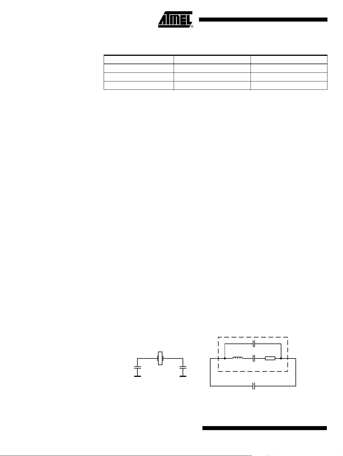
Table 11. Impedance RF_OUT Pin in RX Mode
Frequency Z(RF_OUT)RX RP//C
315 MHz 36 Ω − j 502 Ω 7 kΩ / / 1.0 pF
MHz 19 Ω − j 366 Ω 7 kΩ / / 1.0 pF
433.92
MHz 2.8 Ω − j 141Ω 7 kΩ / / 1.3 pF
868.3
P
Note that if matching to 50 Ω, like in Figure 5 on page 7, a high Q wire wound inductor
with a Q > 70 should be used for L
to minimize its contribution to RX losses which will
2
otherwise be dominant. The RX and TX losses will be in the range of 1.0 dB there.
XTO The XTO is an amplitude regulated Pierce oscillator type with integrated load capaci-
tances (2 × 18 pF with a tolerance of ±17%) hence C
The XTO oscillation frequency f
is the reference frequency FREF for the fractional-N
XTO
= 7.4 pF and C
Lmin
synthesizer. When designing the system in terms of receiving and transmitting frequency offset the accuracy of the crystal and XTO have to be considered.
The synthesizer can adjust the local oscillator frequency for more than ±150 ppm at
433.92 MHz/315 MHz and up to ±118 ppm at 868.3 MHz of initial frequency error in
. This is done at nominal supply voltage and temperature with the control registers 2
f
XTO
and 3 (see Table 20 on page 35 and Table 23 on page 36). The remaining local oscillator tolerance at nominal supply voltage and temperature is then < ±0.5 ppm. A XTO
frequency error of ±150 ppm/±118 ppm can hence be tolerated due to the crystal tolerance at 25°C and the tolerances of C
and CL2. The XTO’s gm has very low influence of
L1
less than ±2 ppm on the frequency at nominal supply voltage and temperature.
= 10.6 pF.
Lmax
Over temperature and supply voltage, the XTO's additional pulling is only ±2 ppm if
≤ 7 fF. The XTAL versus temperature and its aging is then the main source of fre-
C
m
quency error in the local oscillator.
The XTO frequency depends on XTAL properties and the load capacitances C
XTAL1 and XTAL2. The pulling of f
from the nominal f
XTO
is calculated using the fol-
XTAL
L1, 2
at pin
lowing formula:
C
m
--------
P
C
is the crystal's motional, C0 the shunt and CLN the nominal load capacitance of the
m
----------- ------------- ------------- ---------- --------------
× 10
C
2
0CLN
XTAL found in its data sheet. C
circuit and consists of C
C
LNCL
+()C0CL+()×
–
and CL2 in series connection.
L1
6
ppm.
×=
is the total actual load capacitance of the crystal in the
L
Figure 18. XTAL with Load Capacitance
Crystal equivalent circuit
XTAL
C
L1
C
L2
C
0
C
L
m
R
m
m
22
ATA5811/ATA5812 [Preliminary]
CL = CL1 CL2/(CL1 + (CL2)
×
4689B–RKE–04/04
Page 23

ATA5811/ATA5812 [Preliminary]
With C
to P
pulling is P
≤ 14 fF, C0 ≥ 1.5 pF, C
m
≤ ±100 ppm and with Cm ≤ 7 fF, C0 ≥ 1.5 pF, C
≤ ±50 ppm.
= 9 pF and CL = 7.6 pF to 10.6 pF the pulling amounts
LN
= 9 pF and CL = 7.4 pF to 10.6 pF the
LN
Since typical crystals have less than ±50 ppm tolerance at 25° the compensation is not
critical.
C
of the XTAL has to be lower than C
0
/2 = 3.8 pF for a Pierce oscillator type in order
Lmin
to not enter the steep region of pulling versus load capacitance where there is a risk of
an unstable oscillation.
To ensure proper start-up behavior the small signal gain and thus the negative resistance provided by this XTO at start is very large, for example oscillation starts up even in
worst case with a crystal series resistance of 1.5
kΩ at C0 ≤ 2.2 pF with this XTO. The
negative resistance is approximately given by
Z
⎧⎫
1Z3Z2Z3Z1
Re Z
{}Re
xtocore
with Z
, Z2 as complex impedances at pin XTAL1 and XTAL2 hence
1
Z1 = -j/(2 × π × f
Z
consists of crystals C0 in parallel with an internal 110 kΩ resistor hence
3
Z3 = -j/(2 × π × f
------------- ------------- ------------ ----------- ------------- ------------- ------------ ------------- --
=
⎨⎬
Z
⎩⎭
1Z2Z3Z1Z2
× CL1) + 5 Ω and Z2 = -j/(2 × π × f
XTO
× C0) /110 kΩ, gm is the internal transconductance between
XTO
+ Z2× Z3gm×××+×
× gm×+++
× CL2) + 5 Ω.
XTO
XTAL1 and XTAL2 with typically 19 ms at 25°C.
With f
= 13.5 MHz, gm = 19 ms, CL = 9 pF, C0 = 2.2 pF this results in a negative
XTO
resistance of about 2 kΩ. The worst case for technological, supply voltage and temperature variations is then for C
≤ 2.2 pF always higher than 1.5 kΩ.
0
Due to the large gain at start the XTO is able to meet a very low start-up time. The oscillation start-up time can be estimated with the time constant τ.
------------ ------------- ------------ ----------- ------------- ------------- ------------ ------------- -----=
τ
× f
4 π
After 10
2
2
× Cm× Re Z
m
τ to 20 τ an amplitude detector detects the oscillation amplitude and sets
2
()Rm+()×
xtocore
XTO_OK to High if the amplitude is large enough, this sets N_RESET to High and activates the CLK output if CLK_ON in control register 3 is High (see Table 20 on page 35).
Note that the necessary conditions of the VSOUT and DVCC voltage also have to be fulfilled (see Figure 19 on page 24 and Figure 21 on page 26).
To save current in Idle and sleep mode, the load capacitors partially are switched off in
this modes with S1 and S2 seen in Figure 19 on page 24.
It is recommended to use a crystal with C
and C
= 1.5 pF to 2.2 pF.
0
= 4.0 fF to 7.0 fF, CLN = 9 pF, Rm < 120 Ω
m
4689B–RKE–04/04
23
Page 24
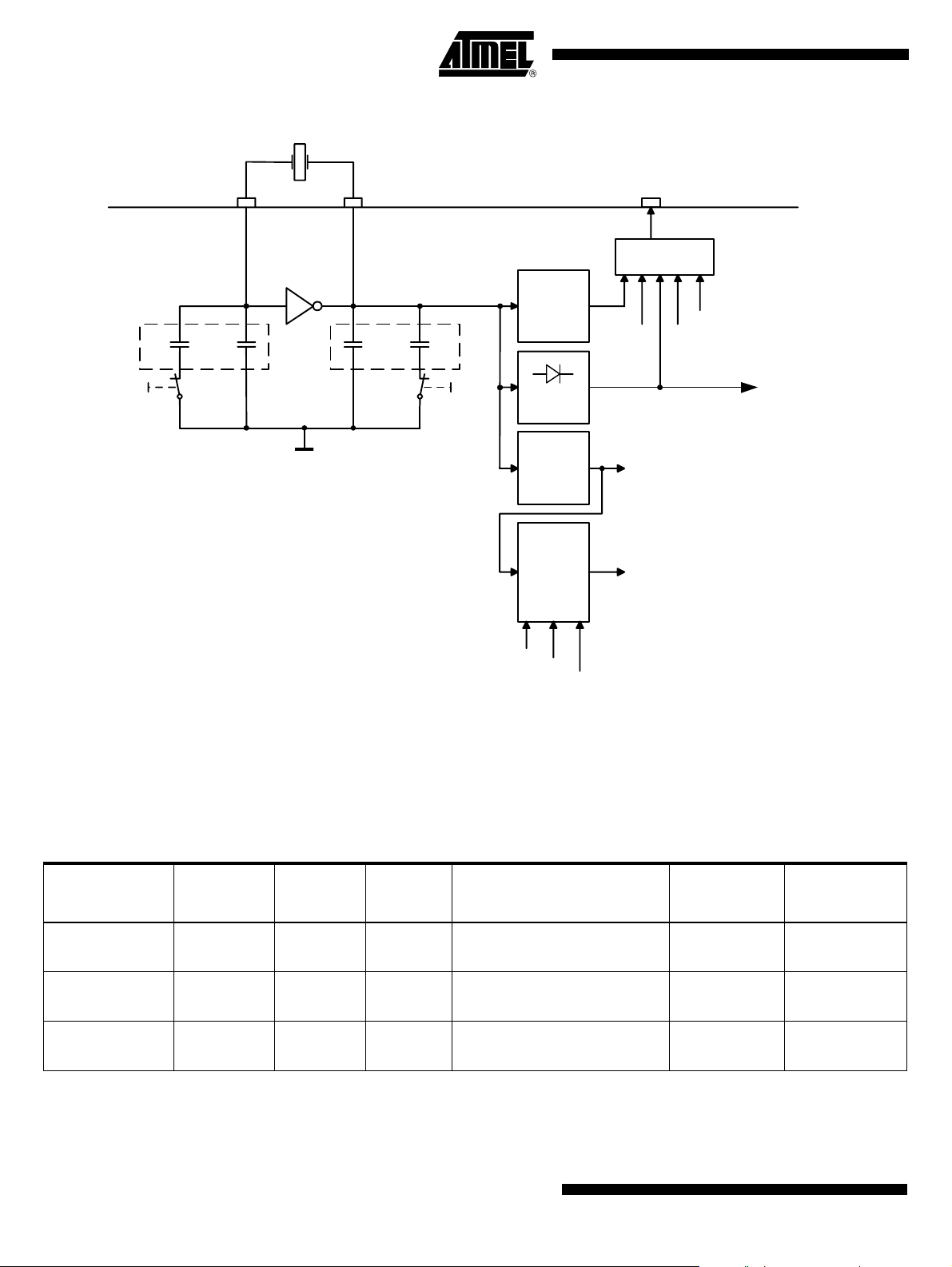
Figure 19. XTO Block Diagram
XTAL1 XTAL2
C
L1
C
8 pF 8 pF
S1 S2
In IDLE mode and during Sleep mode (RX_Polling) the
switches S1 and S2 are open.
10 pF 10 pF
L2
f
XTO
Amplitude
Detector
Baud1
Divider
/3
Divider
/16
Divider
/1
/2
/4
/8
/16
Baud0
CLK_ON
(Control
Register 3)
XLim
CLK
&
VSOUT_OK
(from power supply)
f
DCLK
f
XDCLK
DVCC_OK
(from power supply)
XTO_OK
(to Reset Logic)
To find the right values used in the control registers 2 and 3 (see Table 20 on page 35
and Table 23 on page 36) the relationship between f
and the fRF is shown in
XTO
Table 12. To determine the right content the frequency at pin CLK as well as the output
frequency at RF_OUT in ASK mode can be measured, than the FREQ value can be calculated according to Table 12 so that f
Table 12. Calculation of f
Frequency (MHz)
433.92 AVCC 0 13.25311 f
868.3 GND 0 13.41191 fRF - 16.37 kHz fRF + 16.37 kHz
315.0 AVCC 1 12.73193 fRF - 15.54 kHz fRF + 15.54 kHz
RF
Pin 6
433_N868
CREG1
Bit(4)
FS f
(MHz) f
XTO
= f
RF
⎛⎞
f
f
f
32 5
×
XTO
⎝⎠
⎛⎞
64 5
×
XTO
⎝⎠
⎛⎞
24 5
×
XTO
⎝⎠
is exactly the desired radio frequency
RF
TX_ASK
FREQ 20,5+
------------ ------------ ----------+,
FREQ 20,5+
------------- ------------- --------+,
FREQ 20,5+
------------- ------------- --------+,
= f
RX
16384
16384
16384
f
TX_FSK_L
- 16.17 kHz f
RF
f
TX_FSK_H
+ 16.17 kHz
RF
24
ATA5811/ATA5812 [Preliminary]
4689B–RKE–04/04
Page 25
ATA5811/ATA5812 [Preliminary]
The variable FREQ depends on FREQ2 and FREQ3, which are defined by the bits FR0
to FR8 in control register 2 and 3 and is calculated as follows:
FREQ = 3584 + FREQ2 + FREQ3
Only the range of FREQ = 3803 to 4053 of this register should be used because other-
wise harmonics of f
XTO
and f
(FREQ_min = 3803, FREQ_max = 4053). The resulting tuning range is
MHz and more than ±150 ppm at 433.92 MHz or 315 MHz.
868.3
can cause interference with the received signals
CLK
±118 ppm at
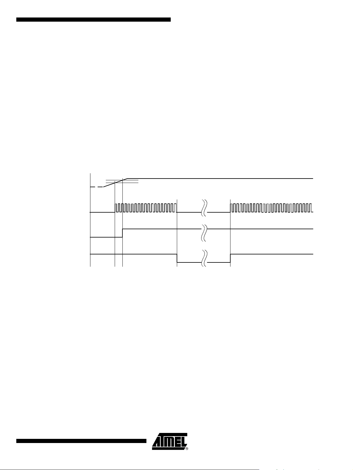
Pin CLK Pin CLK is an output to clock a connected microcontroller. The clock frequency f
calculated as follows:
f
XTO
-----------=
3
V
= 2.3 V (typically)
Thres_1
Figure 20. Clock Timing
VSOUT
CLK
N_RESET
CLK_ON
(Control Register 3)
f
CLK
Because the enabling of pin CLK is asynchronous the first clock cycle may be incomplete. The signal at CLK output has a nominal 50% duty cycle.
V
= 2.38 V (typically)
Thres_2
CLK
is
Basic Clock Cycle of the Digital Circuitry
4689B–RKE–04/04
The complete timing of the digital circuitry is derived from one clock. According to
Figure 19 on page 24, this clock cycle T
is derived from the crystal oscillator (XTO)
DCLK
in combination with a divider.
f
f
DCLK
T
DCLK
XTO
-----------=
16
controls the following application relevant parameters:
• Timing of the polling circuit including Bit-check
• TX baud rate
The clock cycle of the Bit-check and the TX baud rate depends on the selected baud-
rate range (BR_Range) which is defined in control register 6 (see Table 33 on page 38)
and XLim which is defined in control register 4 (see Table 26 on page 36). This clock
cycle T
BR_Range ⇒ BR_Range 0: T
is defined by the following formulas for further reference:
XDCLK
BR_Range 1: T
BR_Range 2: T
BR_Range 3: T
XDCLK
XDCLK
XDCLK
XDCLK
= 8 × T
= 4 × T
= 2 × T
= 1 × T
DCLK
DCLK
DCLK
DCLK
× XLim
× XLim
× XLim
× XLim
25
Page 26
Power Supply
Figure 21. Power Supply
VS1
VS2
VSINT
(Control Register 1)
AVCC_EN
PWR_ON
T1
T5
DVCC_OK
OFFCMD
(Command via SPI)
VS1+
0.55V
VAUX
typ.
IN
≥ 1
≥ 1
S R Q
0 0 no change
0 1 0
1 0 1
1 1 1
P_On_Aux
(Status Register)
V_REG2
3.25 V typ.
V_REG1
IN OUT
3.25 V typ.
EN
FF1
Q
S
R
and
OUT
SW_VSOUT
SW_AVCC
SW_DVCC
V_Monitor
(1.5 V typ.)
V_Monitor
(2.3 V/
2.38 V typ.)
AVCC
DVCC
DVCC_OK
(to XTO and
Reset Logic )
VSOUT_OK
(to XTO and
Reset Logic)
Low_Batt
(Status Register
and Reset Logic)
VSOUT
26
VSOUT_EN
(Control Register 3)
EN
The supply voltage range of the ATA5811/ATA5812 is 2.4 V to 3.6 V or 4.4 V to 6.6 V.
Pin VS1 is the supply voltage input for the range 2.4 V to 3.6 V and is used in battery
applications using a single lithium 3 V cell. Pin VS2 is the voltage input for the range
4.4 V to 6.6 V (2 Battery Application and Car Applications) in this case the voltage regulator V_REG1 regulates VS1 to typically 3.25 V. If the voltage regulator is active a
blocking capacitor of 2.2 µF has to be connected to VS1.
Pin VAUX is an input for an additional auxiliary voltage supply and can be connected
e.g., to an inductive supply (see Figure 26 on page 32). This input can only be used
together with a rectifier or as in the application of Figure 5 on page 7 and must otherwise
be left open.
Pin VSINT is the voltage input for the Microcontoller_Interface and must be connected
to the power supply of the microcontroller. The voltage range of V
(see Figure 25 on page 31 and Figure 26 on page 32).
ATA5811/ATA5812 [Preliminary]
is 2.4 V to 5.25 V
VSINT
4689B–RKE–04/04
Page 27

ATA5811/ATA5812 [Preliminary]
AVCC is the internal operation voltage of the RF transceiver and is feed via the switch
SW_AVCC by VS1. AVCC must be blocked with a 68 nF capacitor (see Figure 4 on
page 6, Figure 5 on page 7 and Figure 6 on page 8).
DVCC is the internal operation voltage of the digital control logic and is feed via the
switch SW_DVCC by VS1 or VSOUT. DVCC must be blocked on pin DVCC with 68 nF
(see Figure 4 on page 6, Figure 5 on page 7 and Figure 6 on page 8).
Pin VSOUT is a power supply output voltage for external devices (e.g., microcontroller)
and is fed via the switch SW_VSOUT by VS1 or via V_REG2 by the a auxiliary voltage
supply VAUX. The voltage regulator V_REG2 regulates VSOUT to typically 3.25 V. If
the voltage regulator is active a blocking capacitor of 2.2 µF has to be connected to
VSOUT. VSOUT can be switched off by the VSOUT_EN bit in control register 3 and is
then reactivated by conditions found in Figure 22 on page 28.
Pin N_RESET is set to low if the voltage V
at pin VSOUT drops below 2.3 V (typi-
VSOUT
cally) and can be used as a reset signal for a connected microcontroller (see Figure 23
on page 30 and Figure 24 on page 31).
Pin PWR_ON is an input to switch on the transceiver (active high).
Pin T1 to T5 are inputs for push buttons and can also be used to switch on the trans-
ceiver (active low).
For current consumption reasons it is recommended to set T1 to T5 to GND or
PWR_ON to VCC only temporarily. Otherwise an additional current flows.
There are two voltage monitors generating the following signals (see Figure 21 on page
26):
• DVCC_OK if DVCC > 1.5 V typically
• VSOUT_OK if VSOUT > V
• Low_Batt if VSOUT < V
Thres2
(2.3 V typically)
Thres1
(2.38 V typically)
4689B–RKE–04/04
27
Page 28

Figure 22. Flow Chart Operation Modes
Bit AVCC_EN = 0 and OFF Command and
Pin PWR_ON = 0 and
Pin T1, T2, T3, T4 and T5 = 1
OFF Mode
AVCC = OFF
V
VAUX
< 3.5 V (typ)
DVCC = OFF
VSOUT = OFF
V
Pin PWR_ON = 1 or
Pin T1, T2, T3, T4 or
T5 = 0
Pin PWR_ON = 1 or
Pin T1, T2, T3, T4 or
V
< VS1+0.5 V
IDLE Mode AUX Mode
AVCC = VS1
DVCC = VS1
VSOUT = VS1
OPM1 OPM0
0 1 TX Mode
1 0 RX Polling Mode
1 1 RX Mode
VAUX
V
VAUX
> VS1+0.5 V
IDLE Mode
AVCC = VS1
DVCC = VS1
VSOUT = V_REG2
OPM1 = 0 and OPM0 = 0
Statusbit Power_On = 1
or
Event on Pin T1, T2, T3, T4 or T5
Pin T5 = 0 or
Bit AVCC_EN = 1
Bit AVCC_EN = 0 and
OFF Command and
Pin PWR_ON = 0 and
Pin T1, T2, T3, T4 and
T5 = 1
VSOUT_EN = 0
> 3.5 V (typ)
VAUX
DVCC = V_REG2
VSOUT = V_REG2
VSOUT = OFF
AVCC = OFF
IDLE Mode
AVCC = VS1
DVCC = VS1
OPM1 = 0 and OPM0 = 1
TX Mode
AVCC = VS1
DVCC = VS1
VSOUT = VS1 or
V_REG2
OPM1 = 0 and OPM0 = 1
OPM1 = 1 and OPM0 = 0
OPM1 = 1 and OPM0 = 1
RX Polling Mode
AVCC = VS1
DVCC = VS1
VSOUT = VS1 or
V_REG2
VSOUT_EN = 0
OPM1 = 1 and OPM0 = 0
OPM1 = 1 and OPM0 = 1
or Bit check ok
Statusbit Power_On = 1
or
Event on Pin T1, T2, T3,
T4 or T5
RX Mode
AVCC = VS1
DVCC = VS1
VSOUT = VS1 or
V_REG2
RX Polling Mode
AVCC = VS1
Bit check ok
DVCC = VS1
VSOUT = OFF
OFF Mode After connecting the power supply (battery) to pin VS1 and/or VS2 and if the voltage on
pin VAUX V
DVCC and VSOUT are disabled, resulting in very low power consumption (I
cally 10 nA). In OFF mode the transceiver is not programmable via the 4-wire serial
interface.
< 3.5 V (typically) the transceiver is in OFF mode. In OFF mode AVCC,
VAUX
S_OFF
is typi-
28
ATA5811/ATA5812 [Preliminary]
4689B–RKE–04/04
Page 29

ATA5811/ATA5812 [Preliminary]
AUX Mode The transceiver changes from OFF mode to AUX mode if the voltage at pin VAUX
> 3.5 V (typically). In AUX mode DVCC and VSOUT are connected to the auxil-
V
VAUX
iary power supply input (VAUX) via the voltage regulator V_REG2. In AUX mode the
transceiver is programmable via the 4-wire serial interface, but no RX or TX operations
are possible because AVCC = OFF.
The state transition OFF mode to AUX mode is indicated by an interrupt at pin IRQ and
the status bit P_On_Aux = 1.
Idle Mode In Idle mode AVCC and DVCC are connected to the battery voltage (VS1).
From OFF mode the transceiver changes to Idle mode if pin PWR_ON is set to 1 or pin
T1, T2, T3, T4 or T5 is set to 0. This state transition is indicated by an interrupt at pin
IRQ and the status bits Power_On = 1 or ST1, ST2, ST3, ST4 or ST5 = 1.
From AUX mode the transceiver changes to Idle mode by setting AVCC_EN = 1 in control register 1 via the 4-wire serial interface or if pin PWR_ON is set to 1 or pin T1, T2,
T3, T4 or T5 is set to 0.
VSOUT is either connected to VS1 or to the auxiliary power supply (V_REG2).
If V
< VS1 + 0.5 V, VSOUT is connected to VS1. If V
VAUX
connected to V_REG2 and the status bit P_On_Aux is set to 1.
> VS1 + 0.5 V, VSOUT is
VAUX
Reset Timing and Reset Logic
In Idle mode the RF transceiver is disabled and the power consumption I
S_IDLE
is about
230 µA (VSOUT OFF and CLK output OFF VS1 = VS2 = 3 V). The exact value of this
current is strongly dependent on the application and the exact operation mode, therefore check the section “Electrical Characteristics” for the appropriate application case.
Via the 4-wire serial interface a connected microcontroller can program the required
parameter and enable the TX, RX polling or RX mode.
The transceiver can be set back to OFF mode by an OFF command via the 4-wire serial
interface (the bit AVCC_EN must be set to 0, the input level of pin PWR_ON must be 0
and pin T1, T2, T3, T4 and T5 = 1 before writing the OFF command).
Table 13. Control Register 1
OPM1 OPM0 Function
0 0 Idle mode
If the transceiver is switched on (OFF mode to Idle mode, OFF mode to AUX mode)
DVCC and VSOUT are ramping up as illustrated in Figure 23 on page 30 (AVCC only
ramps up if the transceiver is set to the Idle mode). The internal signal DVCC_RESET
resets the digital control logic and sets the control register to default values.
A voltage monitor generates a low level at pin N_RESET until the voltage at pin VSOUT
exceeds 2.38 V (typically) and the start-up time of the XTO has elapsed (amplitude
detector, see Figure 19 on page 24). After the voltage at pin VSOUT exceeds 2.3 V (typically) and the start-up time of the XTO has elapsed the output clock at pin CLK is
available. Because the enabling of pin CLK is asynchronous the first clock cycle may be
incomplete.
4689B–RKE–04/04
The status bit Low_Batt is set to 1 if the voltage at pin VSOUT V
V
Thres_2
(typically 2.38 V). Low_Batt is set to 0 if V
VSOUT
exceeds V
VSOUT
Thres_2
register is read via the 4-wire serial interface or N_RESET is set to low.
drops below
and the status
29
Page 30

Figure 23. Reset Timing
= 2.38 V (typ)
V
Thres_2
V
= 2.3 V (typ)
Thres_1
VSOUT
DVCC
(AVCC)
If V
in control register
drops below V
VSOUT
(typically 2.3 V), N_RESET is set to low. If bit VSOUT_EN
Thres_1
3 is 1, a DVCC_RESET is also generated. If V
was prior dis-
VSOUT
abled by the connected microcontroller by setting bit VSOUT_EN = 0, no
DVCC_RESET is generated.
Note: If VSOUT < V
Microcontroller_Interface is disabled and the transceiver is not programmable via the
4-wire serial interface.
1.5 V (typically)
(typically 2.3 V) the output of the pin CLK is low, the
Thres_1
DVCC_RESET
N_RESET
Low_Batt
(Status Register)
VSOUT_EN
(Control Register 3)
CLK
V
> 2.38 V and the XTO is running
VSOUT
V
> 2.3 V and the XTO is running
VSOUT
30
ATA5811/ATA5812 [Preliminary]
4689B–RKE–04/04
Page 31

ATA5811/ATA5812 [Preliminary]
Figure 24. Reset Logic, SR Latch Generates the Hysteresis in the NRESET Signal
DVCC_OK
DVCC_RESET
≥
1
no change
0
no change
NRESET
XTO_OK
VSOUT_OK
LOW_BATT
and
and
VSOUT_EN
SRQ
and
SR Q
Q
0
0
1
1
0
1
011
1-Battery Application The supply voltage range is 2.4 V to 3.6 V and VAUX is not used.
Figure 25. 1-Battery Application
ATA5811/ATA5812
RF - Transceiver
Digital Control
Logic
SDO_TMDO
Microcontroller_Interface
VS1
VS2
VAUX
AVCC
DVCC
VSOUT
VSINT
CS
SCK
SDI_TMDI
IRQ
CLK
NRESET
DEM_OUT
2.4 V to 3.6 V
Microcontroller
VS
OUT
OUT
OUT
IN
IN
IN
IN
4689B–RKE–04/04
31
Page 32

2-Battery Application The supply voltage range is 4.4 V to 6.6 V and VAUX is connected to an inductive
supply.
Figure 26. 2-Battery Application with Inductive Emergency Supply
ATA5811/ATA5812
RF - Transceiver
Digital Control
Logic
Microcontoller_Interface
VS1
VS2
VAUX
AVCC
DVCC
VSOUT
VSINT
CS
SCK
SDI_TMDI
SDO_TMDO
IRQ
CLK
NRESET
DEM_OUT
Microcontroller
4.4 V to 6.6 V
VS
OUT
OUT
OUT
IN
IN
IN
IN
Microcontroller Interface
The microcontroller interface is a level converter which converts all internal digital signals which are referred to the DVCC voltage, into the voltage used by the
microcontroller. Therefore, the pin VSINT has to be connected to the supply voltage of
the microcontroller.
This makes it possible to use the internal voltage regulator/switch at pin VSOUT as in
Figure 4 on page 6 and Figure 6 on page 8 or to connect the microcontroller and the pin
VSINT directly to the supply voltage of the microcontroller as in Figure 5 on page 7.
Digital Control Logic
Register Structure The configuration of the transceiver is stored in RAM cells. The RAM contains a
16 × 8-bit TX/RX data buffer and a 6 × 8-bit control register and is write and readable
via a 4-wire serial interface (CS, SCK, SDI_TMDI, SDO_TMDO).
The 1 × 8-bit status register is not part of the RAM and is readable via the 4-wire serial
interface.
The RAM and the status information is stored as long as the transceiver is in any active
mode (DVCC = VS1 or DVCC = V_REG2) and gets lost if the transceiver is in OFF
mode (DVCC = OFF).
32
ATA5811/ATA5812 [Preliminary]
4689B–RKE–04/04
Page 33

Figure 27. Register Structure
ATA5811/ATA5812 [Preliminary]
After the transceiver is turned on via pin PWR_ON = High, T1 = Low, T2 = Low,
T3 = Low, T4 = Low or T5 = Low or the voltage at pin VAUX V
control registers are in the default state.
> 3.5 V (typically) the
VAUX
MSB
IR1 IR0
----FR8
ASK/
NFSK
AVCC_
FR4 FR3 FR2 FR1 FR0
FR5FR6
Sleep4 Sleep3 Sleep2 Sleep1
EN
FS
-
OPM 1
FR7
Sleep0
OPM 0
VSOUT_
En
XSleep
LSB
T_MODE
P_MODE
CLK_ON
XLim
TX/RX Data Buffer:
16 × 8 Bit
Control Register 1 (ADR 0)
Control Register 2 (ADR 1)
Control Register 3 (ADR 2)
Control Register 4 (ADR 3)
4689B–RKE–04/04
BitChk1 BitChk0
Baud1 Baud0
ST5 ST4 ST3 ST2 ST1
Lim_min5
Lim_max5
Lim_max2Lim_max3Lim_max4
Power_
On
Lim_max1
Low_
Batt
Lim_min0Lim_min1Lim_min2Lim_min3Lim_min4
Lim_max0
P_On_
Aux
Control Register 5 (ADR 4)
Control Register 6 (ADR 5)
Status Register (ADR 8)
33
Page 34

TX/RX Data Buffer The TX/RX data buffer is used to handle the data transfer during RX and TX operations.
Control Register To use the transceiver in different applications it can be configured by a connected
microcontroller via the 4-wire serial interface.
Control Register 1 (ADR 0)
Table 14. Control Register 1 (Function of Bit 7 and Bit 6 in RX Mode)
IR1 IR0 Function (RX Mode)
00
01
10
1 1 Pin IRQ is set to 1 if a receiving error occurred
Table 15. Control Register 1 (Function of Bit 7 and Bit 6 in TX Mode)
IR1 IR0 Function (TX Mode)
00
01
10
1 1 Pin IRQ is set to 1 if the TX data buffer is empty
Pin IRQ is set to 1 if 4 received bytes are in the TX/RX data buffer or a receiving
error occurred
Pin IRQ is set to 1 if 8 received bytes are in the TX/RX data buffer or a receiving
error occurred
Pin IRQ is set to 1 if 12 received bytes are in the TX/RX data buffer or a receiving
error occurred (default)
Pin IRQ is set to 1 if 4 bytes still are in the TX/RX data buffer or the TX data buffer
is empty
Pin IRQ is set to 1 if 8 bytes still are in the TX/RX data buffer or the TX data buffer
is empty
Pin IRQ is set to 1 if 12 bytes still are in the TX/RX data buffer or the TX data buffer
is empty (default)
Table 16. Control Register 1 (Function of Bit 5)
AVCC_EN Function
0 (default)
1 Enables AVCC, if the ATA5811/
ATA5812 is in AUX mode
Table 17. Control Register 1 (Function of Bit 4)
FS Function
0 433/868 MHz
1315 MHz
34
ATA5811/ATA5812 [Preliminary]
4689B–RKE–04/04
Page 35

Control Register 2 (ADR 1)
ATA5811/ATA5812 [Preliminary]
Table 18. Control Register 1 (Function of Bit 2 and Bit 1)
OPM1 OPM0 Function
0 0 Idle mode (default)
01TX mode
1 0 RX polling mode
11RX mode
Table 19. Control Register 1 (Function of Bit 0)
T_MODE Function
0 TX and RX function via TX/RX data buffer (default)
1
Table 20. Control Register 2 (Function of Bit 7, Bit 6, Bit 5, Bit 4, Bit 3, Bit 2 and Bit 1)
FR6 FR5 FR4 FR3 FR2 FR1 FR0 Function
0000000FREQ2 = 0
0000001FREQ2 = 1
.......
1011000FREQ2 = 88 (default)
.......
1111111FREQ2 = 127
Note: Tuning of f
Transparent mode, TX/RX data buffer disabled, TX modulation data stream via
pin SDI_TMDI, RX modulation data stream via pin SDO_TMDO
LSB’s (total 9 bits), frequency trimming, resolution of f
which is approximately 800 Hz (see section “XTO”, Table 12 on page 24)
RF
RF
is f
XTO
/16384
Table 21. Control Register 2 (Function of Bit 0 in RX Mode)
P_MODE Function (RX Mode)
0 Pin IRQ is set to 1 if the Bit-check is successful (default)
1 No effect on pin IRQ if the Bit-check is successful
Table 22. Control Register 2 (Function of Bit 0 in TX Mode)
P_MODE Function (TX Mode)
0 Manchester modulator on (default)
1 Manchester modulator off (NRZ mode)
4689B–RKE–04/04
35
Page 36

Control Register 3 (ADR 2)
Table 23. Control Register 3 (Function of Bit 3 and Bit 2)
FR8 FR7 Function
00FREQ3 = 0
0 1 FREQ3 = 128
1 0 FREQ3 = 256 (default)
1 1 FREQ3 = 384
Note: Tuning of f
RF
MSB’s
Table 24. Control Register 3 (Function of Bit 1)
VSOUT_EN Function
0 Output voltage power supply for external devices off (pin VSOUT)
1 Output voltage power supply for external devices on (default)
Note: This bit is set to 1 if the Bit-check is ok (RX_Polling, RX mode), an event at pin T1, T2,
T3, T4 or T5 occurs or the bit Power_On in the status register is 1.
Setting VSOUT_EN = 0 in AUX mode is not allowed
Table 25. Control Register 3 (Function of Bit 0)
CLK_ON Function
0 Clock output off (pin CLK)
1 Clock output on (default)
Note: This bit is set to 1 if the Bit-check is ok (RX_Polling, RX mode), an event at pin T1, T2,
T3, T4 or T5 occurs or the bit Power_On in the status register is 1.
Control Register 4 (ADR 3)
Table 26. Control Register 4 (Function of Bit 7)
ASK_NFSK Function
0 FSK mode (default)
1 ASK mode
Table 27. Control Register 4 (Function of Bit 6, Bit 5, Bit 4, Bit 3 and Bit 2)
Function Sleep
Sleep4 Sleep3 Sleep2 Sleep1 Sleep0
00000 0
00001 1
.....
01010
.....
11111 31
(T
= Sleep × 1024 × T
Sleep
= 10 × 1024 × T
(T
Sleep
10
(default)
DCLK
DCLK
× X
× X
Sleep
Sleep
)
)
36
ATA5811/ATA5812 [Preliminary]
4689B–RKE–04/04
Page 37

Control Register 5 (ADR 4)
ATA5811/ATA5812 [Preliminary]
Table 28. Control Register 4 (Function of Bit 1)
XSleep Function
0X
1X
= 1; extended T
Sleep
= 8; extended T
Sleep
Table 29. Control Register 4 (Function of Bit 0)
XLim Function
0X
1X
= 1; extended TLim_min, TLim_max off (default)
Lim
= 2; extended T
Lim
Table 30. Control Register 5 (Function of Bit 7 and Bit 6)
BitChk1 BitChk0 Function
00N
01N
10N
11N
Bit-check
Bit-check
Bit-check
Bit-check
off (default)
Sleep
on
Sleep
Lim_min
, T
Lim_max
on
= 0 (0 bits checked during Bit-check)
= 3 (3 bits checked during Bit-check (default))
= 6 (6 bits checked during Bit-check)
= 9 (9 bits checked during Bit-check)
Table 31. Control Register 5 (Function of Bit 5, Bit 4, Bit 3, Bit 2, Bit 1 and Bit 0 in RX Mode)
Function (RX Mode)
Lim_min
(Lim_min < 10 are not applicable)
Lim_min5 Lim_min4 Lim_min3 Lim_min2 Lim_min1 Lim_min0
001010 10
001011 11
......
010000
......
111111 63
(T
Lim_min
(T
Lim_min
= Lim_min × T
16
= 16 × T
(default)
XDCLK
XDCLK
)
)
4689B–RKE–04/04
37
Page 38

Table 32. Control Register 5 (Function of Bit 5, Bit 4, Bit 3, Bit 2, Bit 1 and Bit 0 in TX Mode)
Function (TX Mode) Lim_min
(Lim_min < 10 are not applicable)
Lim_min5 Lim_min4 Lim_min3 Lim_min2 Lim_min1 Lim_min0
001010 10
001011 11
......
(TX_Baudrate = 1/((Lim_min + 1) × T
XDCLK
× 2)
01000016(TX_Baudrate = 1/((16 + 1) × T
(default)
......
111111 63
Control Register 6 (ADR 5)
Table 33. Control Register 6 (Function of Bit 7 and Bit 6)
Baud1 Baud0 Function
00
01
10
Baud-rate range 0 (B0) 1.0 kBaud to 2.5 kBaud;
T
XDCLK
= 8 × T
DCLK
× X
Lim
Baud-rate range 1 (B1) 2.0 kBaud to 5.0 kBaud;
T
XDCLK
= 4 × T
DCLK
× X
Lim
Baud-rate range 2 (B2) 4.0 kBaud to 10.0 kBaud;
T
XDCLK
= 2 × T
DCLK
× X
; (default)
Lim
Baud-rate range 3 (B3) 8.0 kBaud to 20.0 kBaud;
11
T
XDCLK
= 1 × T
DCLK
× X
Lim
,
Note that the receiver is not working with >10 kBaud in ASK mode
Table 34. Control Register 6 (Function of Bit 5, Bit 4, Bit 3, Bit 2, Bit 1 and Bit 0)
Function Lim_max
(Lim_max < 12 Are Not Applicable)
Lim_max5 Lim_max4 Lim_max3 Lim_max2 Lim_max1 Lim_max0
001100 12
001101 13
......
(T
Lim_max
= (Lim_max - 1) × T
XDCLK
XDCLK
× 2)
)
01110028(T
Lim_max
= (28 - 1) × T
(default)
......
111111 63
38
ATA5811/ATA5812 [Preliminary]
)
XDCLK
4689B–RKE–04/04
Page 39

ATA5811/ATA5812 [Preliminary]
Status Register The status register indicates the current status of the transceiver and is readable via the
4-wire serial interface. Setting Power_On or P_On_Aux or an event on ST1, ST2, ST3,
ST4 or ST5 is indicated by an IRQ.
Reading the status register resets the bits Power_On, Low_Batt, P_On_Aux and the
IRQ
Status Register (ADR 8)
Table 35. Status Register
Status Bit Function
ST5 Status of pin T5
Pin T5 = 0 → ST5 = 1
Pin T5 = 1 → ST5 = 0
(see Figure 29 on page 41)
ST4 Status of pin T4
Pin T4 = 0 → ST4 = 1
Pin T4 = 1 → ST4 = 0
(see Figure 29 on page 41)
ST3 Status of pin T3
Pin T3 = 0 → ST3 = 1
Pin T3 = 1 → ST3 = 0
(see Figure 29 on page 41)
ST2 Status of pin T2
Pin T2 = 0 → ST2 = 1
Pin T2 = 1 → ST2 = 0
(see Figure 29 on page 41)
ST1 Status of pin T1
Pin T1 = 0 → ST1 = 1
Pin T1 = 1 → ST1 = 0
(see Figure 29 on page 41)
Power_On
Low_Batt Indicates that output voltage on pin VSOUT is too low
P_On_Aux Indicates that the auxiliary supply voltage on pin VAUX is high enough to operate.
Indicates that the transceiver was woken up by pin PWR_ON (rising edge on pin
PWR_ON). During Power_On = 1, the bits VSOUT_EN and CLK_ON in control
register 3 are set to 1.
(see Figure 30 on page 42)
(V
(see Figure 31 on page 43)
State transition:
a) OFF mode → AUX mode (see Figure 22 on page 28)
b) Idle mode (VSOUT = VS1) → Idle mode (VSOUT = V_REG2)
(see Figure 32 on page 44)
< 2.38 V typically)
VSOUT
4689B–RKE–04/04
39
Page 40

Pin Tn To switch the transceiver from OFF to Idle mode, pin Tn must set to 0 (maximum
× V
0.2
) for at least T
VS2
edge, sets pin N_RESET to low and switches on DVCC, AVCC and the power supply for
external devices VSOUT.
(see Figure 28). The transceiver recognize the negative
Tn_IRQ
If V
DVCC
and sets the status bit STn to 1 and an interrupt is issued (T
After the voltage on pin VSOUT exceeds 2.3 V (typically) and the start-up time of the
XTO is elapsed the output clock on pin CLK is available. Because the enabling of pin
CLK is asynchronous the first clock cycle may be incomplete. N_RESET is set to high if
V
VSOUT
Figure 28. Timing Pin Tn, Status Bit STn
Tn
V
= 2.38 V (typ)
Thres_2
VSOUT
DVCC, AVCC
N_RESET
1.5 V (typ)
exceeds 1.5 V (typically) and the XTO is settled, the digital control logic is active
).
Tn_IRQ
exceeds 2.38 V (typically) and the XTO is settled.
V
= 2.3 V (typ)
Thres_1
CLK
STn
(Status Register)
IRQ
OFF
Mode
T
Tn_IRQ
IDLE
Mode
40
ATA5811/ATA5812 [Preliminary]
4689B–RKE–04/04
Page 41

If the transceiver is in any active mode (Idle, AUX, TX, RX, RX_Polling), an integrated
debounce logic is active. If there is an event on pin Tn a debounce counter is set to 0
= 0) and started. The status is updated, an interrupt is issued and the debounce
(T
counter is stopped after reaching the counter value T = 8195
An event on the same key input before reaching T = 8195 × T
counter. An event on an other key input before reaching T = 8195
restarts the debounce counter.
While the debounce counter is running, the bits VSOUT_EN and CLK_ON in control
register 3 are set to 1.
The interrupt is deleted after reading the status register or executes the command
Delete_IRQ.
If a pin Tn is not used, it can be left open because of an internal pull-up resistor (typically
50 k
Ω).
Figure 29. Timing Flow Pin Tn, Status Bit STn
IDLE Mode or
AUX Mode or
TX Mode or
RX Polling Mode or
RX Mode
ATA5811/ATA5812 [Preliminary]
× T
.
DCLK
stops the debounce
DCLK
× T
resets and
DCLK
Event on Pin Tn ?
Y
T = 0
Start debounce counter
Event on Pin
Tn ?
Y
Tn = STn ?
Y
Stop debounce counter
N
N
T = 8195 × T
N
Pin Tn = 0 ?
Stop debounce counter
?
Y
Y
STn = 1;
IRQ = 1
N
N
Stop debounce counter
STn = 0;
IRQ = 1
4689B–RKE–04/04
41
Page 42

Pin PWR_ON To switch the transceiver from OFF to Idle mode, pin PWR_ON must set to 1 (minimum
× V
0.8
) for at least T
VS2
PWR_ON
edge, sets pin N_RESET to low and switches on DVCC, AVCC and the power supply for
external devices VSOUT.
(see Figure 30). The transceiver recognize the positive
If V
exceeds 1.5 V (typically) and the XTO is settled, the digital control logic is active
DVCC
and sets the status bit Power_On to 1 and an interrupt is issued (T
After the voltage on pin VSOUT exceeds 2.3 V (typically) and the start-up time of the
XTO is elapsed the output clock on pin CLK is available. Because the enabling of pin
CLK is asynchronous the first clock cycle may be incomplete. N_RESET is set to high if
V
exceeds 2.38 V (typically) and the XTO is settled.
VSOUT
If the transceiver is in any active mode (Idle, AUX, RX, RX_Polling, TX), a positive edge
on pin PWR_ON sets Power_On to 1 (after T
Power_On 0
→ 1 generates an interrupt. If Power_On is still 1 during the positive edge
on pin PWR_ON no interrupt is issued. Power_On and the interrupt is deleted after
reading the status register.
During Power_On = 1, the bits VSOUT_EN and CLK_ON in control register 3 are set
to 1.
Note: It is not possible to set the transceiver to OFF mode by setting pin PWR_ON to 0. If pin
PWR_ON is not used, it must be connected to GND.
Figure 30. Timing Pin PWR_ON, Status Bit Power_On
T
> T
PWR_ON
V
Thres_2
PWR_ON
= 2.38 V (typ)
PWR_ON_IRQ_1
T
PWR_ON
> T
PWR_ON_IRQ_2
PWR_ON_IRQ_2
PWR_ON_IRQ_1
).
). The state transition
VSOUT
DVCC, AVCC
N_RESET
CLK
Power_On
(Status Register)
IRQ
1.5 V (typ)
OFF
Mode
T
PWR_ON_IRQ_1
IDLE
Mode
V
Thres_1
= 2.3 V (typ)
T
PWR_ON_IRQ_2
IDLE, AUX, RX, RX Polling, TX
Mode
42
ATA5811/ATA5812 [Preliminary]
4689B–RKE–04/04
Page 43

ATA5811/ATA5812 [Preliminary]
Low Battery Indicator The status bit Low_Batt is set to 1 if the voltage on pin VSOUT V
2.38 V (typically).
Low_Batt is set to 0 if V
4-wire serial interface (see Figure 23 on page 30).
Figure 31. Timing Status Bit Low_Batt
exceeds V
VSOUT
IDLE, AUX, TX, RX or
RX Polling Mode
V
VSOUT
Low_Batt = 1
Thres_2
< 2.38 V (typ)
?
Yes
and the status register is read via the
No
drops under
VSOUT
Read Status Register
4689B–RKE–04/04
43
Page 44

Pin VAUX To switch the transceiver from OFF to AUX mode, the voltage on pin VAUX V
exceed 3.5 V (typically) (see Figure 32). If V
is set to low, DVCC and the power supply for external devices VSOUT are switched on.
exceeds 2 V (typically) pin N_RESET
VAUX
VAUX
must
If V
exceeds 3.5 V (typically) the status bit P_On_Aux is set to 1 and an interrupt is
VAUX
issued.
After the voltage on pin VSOUT exceeds 2.3 V (typically) and the start-up time of the
XTO is elapsed the output clock on pin CLK is available. Because the enabling of pin
CLK is asynchronous the first clock cycle may be incomplete. N_RESET is set to high if
V
exceeds 2.38 V (typically) and the XTO is settled.
VSOUT
If the transceiver is in any active mode (Idle, TX, RX, RX_Polling), a positive edge on pin
VAUX and V
VAUX
1 generates an interrupt. If P_On_Aux is still 1 during the positive edge on pin VAUX no
interrupt is issued. P_On_Aux and the interrupt is deleted after reading the status
register.
Figure 32. Timing Pin VAUX, Status Bit P_On_Aux
VAUX
VSOUT
DVCC
3.5 V (typ)
2.0 V (typ)
V
= 2.38 V (typ)
Thres_2
V
= 2.3 V (typ)
Thres_1
> VS1 + 0.5 V sets P_On_Aux to 1. The state transition P_On_Aux 0 →
> VS1 + 0.5 V (typ)
V
VAUX
V
> VS1 + 0.5 V (typ)
VAUX
N_RESET
CLK
P_On_Aux
(Status Register)
IRQ
OFF
Mode
AUX
Mode
IDLE, TX, RX, RX Polling
Mode
44
ATA5811/ATA5812 [Preliminary]
4689B–RKE–04/04
Page 45

ATA5811/ATA5812 [Preliminary]
Transceiver Configuration
The configuration of the transceiver takes place via a 4-wire serial interface (CS, SCK,
SDI_TMDI, SDO_TMDO) and is organized in 8-bit units. The configuration is initiated
with a 8-bit command. While shifting the command into pin SDI_TMDI, the number of
bytes in the TX/RX data buffer are available on pin SDO_TMDO. The read and write
commands are followed by one or more 8-bit data units. Each 8-bit data transmission
begins with the MSB. The serial interface is in reset state if the level on pin CS = Low.
Command: Read TX/RX Data Buffer
During a RX operation the user can read the received bytes in the TX/RX data buffer
successively.
Figure 33. Read TX/RX Data Buffer
MSB LSB MSB LSB LSBMSB
SDI_TMDI
SDO_TMDO
SCK
CS
Command: Write TX/RX Data Buffer
Command: Read TX/RX Data Buffer
Nr. Bytes in the TX/RX Data Buffer
During a TX operation the user can write the bytes in the TX/RX data buffer successively. An echo of the command and the TX data bytes are provided for the
microcontroller on pin SDO_TMDO.
X
RX Data Byte 1
X
RX Data Byte 2
Figure 34. Write TX/RX Data Buffer
MSB LSB MSB LSB MSB LSB
SDI_TMDI
SDO_TMDO
SCK
CS
Command: Read
Command: Write TX/RX Data Buffer
Nr. Bytes in the TX/RX Data Buffer
The control and status registers can be read individually or successively.
Control/Status Register
Figure 35. Read Control/Status Register
MSB LSB MSB LSB
SDI_TMDI
SDO_TMDO
SCK
CS
Command: Read C/S Register X
Nr. Bytes in the TX/RX Data Buffer
TX Data Byte 1 TX Data Byte 2
Write TX/RX Data Buffer TX Data Byte 1
MSB LSB
Command: Read C/S Register Y
Data C/S Register X
Command: Read C/S Register Z
Data C/S Register Y
4689B–RKE–04/04
45
Page 46

Command: Write Control Register
Figure 36. Write Control Register
The control registers can be written individually or successively. An echo of the command and the data bytes are provided for the microcontroller on pin SDO_TMDO.
SDI_TMDI
SDO_TMDO
SCK
CS
Command: OFF Command
MSB LSB MSB LSB
Command: Write Control Register X
Nr. Bytes in the TX/RX Data Buffer
Data Control Register X
Write Control Register X
If AVCC_EN in control register 1 is 0, the input level on pin PWR_ON is low and on the
key inputs Tn is high, the OFF command sets the transceiver in the OFF mode.
Figure 37. OFF Command
SDI_TMDI
SDO_TMDO
SCK
CS
MSB LSB
Command: Write Control Register Y
Data Control Register X
MSB LSB
Command: OFF Command
Nr. Bytes in the TX/RX Data Buffer
Command: Delete IRQ The delete IRQ command sets pin IRQ to low.
Figure 38. Delete IRQ
MSB LSB
SDI_TMDI
SDO_TMDO
SCK
CS
Command: Delete IRQ
Nr. Bytes in the TX/RX Data Buffer
Command Structure The three most significant bits of the command (Bit 5 to Bit 7) indicates the command
type. Bit 0 to Bit 4 describes the target address when reading or writing a control or status register. In all other commands Bit 0 to Bit 4 have no effect and should be set to 0 for
compatibility reasons with future products.
46
ATA5811/ATA5812 [Preliminary]
4689B–RKE–04/04
Page 47

ATA5811/ATA5812 [Preliminary]
.
Table 36. Command Structure
MSB LSB
Command
Read TX/RX data buffer 0 0 0 x x x x x
Write TX/RX data buffer 0 0 1 x x x x x
Read control/status register 0 1 0 A4 A3 A2 A1 A0
Write control register 0 1 1 A4 A3 A2 A1 A0
OFF command 10 0XXXXX
Delete IRQ 1 0 1 X X X X X
Not used 1 1 0 X X X X X
Not used 1 1 1 X X X X X
4-wire Serial Interface The 4-wire serial interface consists of the Chip Select (CS), the Serial ClocK (SCK), the
Serial Data Input (SDI_TMDI) and the Serial Data Output (SDO_TMDO). Data is transmitted/received bit by bit in synchronization with the serial clock.
Note: If the output level on pin N_RESET is low, no data communication with the microcontrol-
ler is possible.
Bit 7 Bit 6 Bit 5 Bit 4 Bit 3 Bit 2 Bit 1 Bit 0
Figure 39. Serial Timing
CS
T
SCK_setup1
SCK
SDI_TMDI
SDO_TMDO
When CS is low and the transparent mode is inactive (T_MODE = 0), SDO_TMDO is in
a high-impedance state. When CS is low and the transparent mode is active
(T_MODE = 1), the RX data stream is available on pin SDO_TMDO.
T
CS_setup
X
T
Setup
XMSB
T
Out_enable
X can be either Vil or V
T
iH
Hold
MSB
T
CS_disable
T
Cycle
X
T
Out_delay
MSB-1
X
MSB-1
T
SCK_setup2
LSB
X
T
SCK_hold
X
T
Out_disable
4689B–RKE–04/04
47
Page 48

Operation Modes
RX Operation The transceiver is set to RX operation with the bits OPM0 and OPM1 in control
register 1
.
Table 37.
The transceiver is designed to consume less than 1 mA in RX operation while being
sensitive to signals from a corresponding transmitter. This is achieved via the polling circuit. This circuits enables the signal path periodically for a short time. During this time
the Bit-check logic verifies the presence of a valid transmitter signal. Only if a valid signal is detected the transceiver remains active and transfers the data to the connected
microcontroller. This transfer take place either via the TX/RX data buffer or via the pin
SDO_TMDO. If there is no valid signal present the transceiver is in sleep mode most of
the time resulting in low current consumption. This condition is called RX polling mode.
A connected microcontroller can be disabled during this time.
All relevant parameters of the polling logic can be configured by the connected microcontroller. This flexibility enables the user to meet the specifications in terms of current
consumption, system response time, data rate etc.
Control Register 1
OPM1 OPM0 Function
1 0 RX polling mode
11 RX mode
In RX mode the RF transceiver is enabled permanently and the Bit-check logic verifies
the presence of a valid transmitter signal. If a valid signal is detected the transceiver
transfers the data to the connected microcontroller. This transfer take place either via
the TX/RX data buffer or via the pin SDO_TMDO.
RX Polling Mode If the transceiver is in RX polling mode it stays in a continuous cycle of three different
modes. In sleep mode the RF transceiver is disabled for the time period T
suming low current of I
T
Startup_Sig_Proc
, all signal processing circuits are enabled and settled. In the following
S
= I
. During the start-up period, T
IDLE_X
while con-
Sleep
Startup_PLL
and
Bit-check mode, the incoming data stream is analyzed bit by bit contra a valid transmitter signal. If no valid signal is present, the transceiver is set back to sleep mode after the
period T
age value for T
current consumption is I
sumption is I
. This period varies check by check as it is a statistical process. An aver-
Bit-check
Bit-check
= I
S
is given in the electrical characteristics. During T
= I
S
Startup_Sig_Proc_X
RX_X
. During T
Startup_Sig_Proc
and T
. The condition of the transceiver is indicated on pin
the current con-
Bit-check
Startup_PLL
the
RX_ACTIVE (see Figure 40 on page 50 and Figure 41 on page 51). The average current consumption in RX polling mode I
application or car application. To calculate I
is different in 1 battery application, 2 battery
P
the index X must be replaced by VS1, 2 in
P
1 battery application, VS2 in 2 battery application or VS2, VAUX in car application (see
section “Electrical Characteristics”)
I
IDLE_XTSleepIStartup_PLL_X
I
------------ ------------ ------------- ----------- ------------- ------------ ------------- ------------- ---------- ------------- ------------- ------------- ---------- ------------- ------------- ------------- ------------ ----------=
P
T
++ +
SleepTStartup_PLLTStartup_Sig_ProcTBit_check
T×
Startup_PLL
I
RX_XTStartup_Sig_ProcTBitcheck
+()×++×
48
ATA5811/ATA5812 [Preliminary]
4689B–RKE–04/04
Page 49

ATA5811/ATA5812 [Preliminary]
To save current it is recommended CLK and V
mode. I
does not include the current of the Microcontroller_Interface I
P
rent of an external device connected to pin VSOUT (e.g., microcontroller). If CLK
and/or VSOUT is enabled during RX polling mode the current consumption is calculated
as follows:
I
S_PollIPIVSINTIEXT
During T
++=
Sleep
, T
Startup_PLL
ter signal. To guarantee the reception of a transmitted command the transmitter
must start the telegram with an adequate preburst. The required length of the
preburst T
and T
Bit-check
(N
.
T
) to be tested
Bit-check
PreburstTSleepTStartup_PLLTStartup_Sig_ProcTBit_check
depends on the polling parameters T
Preburst
. Thus, T
++ +≥
Sleep Mode The length of period T
extension factor X
cycle T
T
Sleep
DCLK
Sleep 1024 T
Sleep
. It is calculated to be:
In US and European applications, the maximum value of T
set to 1 (which is done by setting the bit XSleep in control register 4 to 0). The time resolution is about 1.2 ms in that case. The sleep time can be extended to about 300 ms by
setting X
to 8 (which is done by setting XSleep in control register 4 to 1), the time
Sleep
resolution is then about 9.6 ms.
be disabled during RX polling
VSOUT
and T
Startup_Sig_Proc
Bit-check
depends on the actual bit rate and the number of bits
is defined by the 5-bit word sleep in control register 4, the
Sleep
the transceiver is not sensitive to a transmit-
, T
Sleep
Startup_PLL
and the cur-
VSINT
, T
Startup_Sig_Proc
defined by the bit XSleep in control register 4 and the basic clock
×××=
DCLKXSleep
is about 38 ms if X
Sleep
Sleep
is
Start-up Mode During T
cessing circuit starts up (T
condition and ready to receive.
Startup_PLL
the PLL is enabled and starts up. If the PLL is locked, the signal pro-
Startup_Sig_Proc
). After the start-up time all circuits are in stable
4689B–RKE–04/04
49
Page 50

Figure 40. Flow Chart Polling Mode/RX Mode (T_MODE = 1, Transparent Mode Inactive)
Start RX Polling Mode
Sleep mode:
All circuits for analog signal processing are disabled. Only XTO and Polling logic
is enabled.
Output level on pin RX_ACTIVE -> Low; I
T
= Sleep × 1024 × T
Sleep
DCLK
× X
Sleep
= I
S
IDLE_X
Start RX Mode
Start-up mode:
Start-up PLL:
The PLL is enabled and locked.
Output level on pin RX_ACTIVE -> High; I
Start-up signal processing:
The signal processing circuit are enabled.
Output level on pin RX_ACTIVE -> High; I
T
Startup_Sig_Proc
Bit-check mode:
The incomming data stream is analyzed. If the timing indicates a valid transmitter
signal, the control bits VSOUT_EN, CLK_ON and OPM0 are set to 1 and the
transceiver is set to receiving mode. Otherwise it is set to Sleep mode or to
Start-up mode.
Output level on Pin RX_ACTIVE -> High
= I
I
S
RX_X
T
Bit-check
OPM0 = 1
?
NO
YES
NO
T
SLEEP
= 0
?
YES
NO
NO
= I
S
= I
S
Startup_PLL_X ;TStartup_PLL
RX_X
Bit check
OK ?
YES
Set VSOUT_EN = 1
Set CLK_ON = 1
Set OPM0 = 1
P_MODE = 0
?
YES
Set IRQ
Sleep: Defined by bits Sleep0 to Sleep4 in Control
: Defined by bit XSleep in Control Register 4
X
Sleep
: Basic clock cycle
T
DCLK
:798.5
T
Startup_PLL
T
Startup_Sig_Proc
: Depends on the result of the bit check.
T
Bit-check
Register 4
×
T
(typ)
DCLK
:882 × T
DCLK
×
T
498
DCLK
×
T
306
DCLK
×
T
210
DCLK
Is defined by the selected baud rate range and
T
. The baud-rate range is defined by bit
DCLK
Baud0 and Baud1 in Control Register 6.
If the bit check is ok, T
number of bits to be checked (N
on the utilized data rate.
If the bit check fails, the average time period for
that check depends on the selected baud-rate
range and on T
defined by bit Baud0 and Baud1 in Control
Register 6.
(BR_Range 0)
(BR_Range 1)
(BR_Range 2)
(BR_Range 3)
Bit-check
. The baud-rate range is
XDCLK
depends on the
) and
Bit-check
50
Receiving mode:
The incomming data stream is passed via the TX/RX Data Buffer to the
connected microcontroller. If an bit error occurs the transceiver is set back to
Start-up mode.
Output level on pin RX_ACTIVE -> High
= I
I
S
RX_X
Start bit
detected ?
NO
YES
RX data stream is
written into the TX/RX
Data Buffer
Bit error ?
NO
YES
ATA5811/ATA5812 [Preliminary]
If the transceiver detects a bit error after a
successful bit check and before the start bit is
detected pin IRQ will be set to high (only if
P_MODE=0) and the transceiver is set back to
start-up mode.
4689B–RKE–04/04
Page 51

ATA5811/ATA5812 [Preliminary]
Figure 41. Flow Chart Polling Mode/RX Mode (T_MODE = 1, Transparent Mode Active)
Start RX Polling Mode
Sleep mode:
All circuits for analog signal processing are disabled. Only XTO and Polling logic
is enabled.
Output level on pin RX_ACTIVE -> Low; I
T
= Sleep × 1024 × T
Sleep
DCLK
× X
Sleep
= I
S
IDLE_X
Start RX Mode
Start-up mode:
Start-up PLL:
The PLL is enabled and locked.
Output level on pin RX_ACTIVE -> High; I
Start-up signal processing:
The signal processing circuit are enabled.
Output level on pin RX_ACTIVE -> High; I
T
Startup_Sig_Proc
Bit-check mode:
The incomming data stream is analyzed. If the timing indicates a valid transmitter
signal, the control bits VSOUT_EN, CLK_ON and OPM0 are set to 1 and the
transceiver is set to receiving mode. Otherwise the transceiver is set to Sleep
mode (if OPM0 = 0 and T
Output level on Pin RX_ACTIVE -> High
I
= I
S
RX_X
T
Bit-check
OPM0 = 1
?
> 0) or stays in Bit-check mode.
SLEEP
NO
YES
NO
T
SLEEP
= 0
?
YES
NO
= I
S
= I
S
Startup_PLL_X ;TStartup_PLL
RX_X
Bit check
OK ?
YES
Set VSOUT_EN = 1
Set CLK_ON = 1
Set OPM0 = 1
Sleep: Defined by bits Sleep0 to Sleep4 in Control
: Defined by bit XSleep in Control Register 4
X
Sleep
: Basic clock cycle
T
DCLK
T
: 798.5 × T
Startup_PLL
T
Startup_Sig_Proc
: Depends on the result of the bit check.
T
Bit-check
Register 4
(typ)
DCLK
: 882 × T
DCLK
× T
498
DCLK
× T
306
DCLK
× T
210
DCLK
Is defined by the selected baud rate range and
T
. The baud-rate range is defined by bit
DCLK
Baud0 and Baud1 in Control Register 6.
If the bit check is ok, T
number of bits to be checked (N
on the utilized data rate.
If the bit check fails, the average time period for
that check depends on the selected baud-rate
range and on T
defined by bit Baud0 and Baud1 in Control
Register 6.
(BR_Range 0)
(BR_Range 1)
(BR_Range 2)
(BR_Range 3)
Bit-check
. The baud-rate range is
XDCLK
depends on the
) and
Bit-check
4689B–RKE–04/04
Receiving mode:
The incomming data stream is passed via pin SDO_TMDO to the connected
microcontroller. If an bit error occurs the transceiver is not set back to Start-up
mode.
Output level on Pin RX_ACTIVE -> High
= I
I
S
RX_X
Level on pin CS = Low ?
NO
YES
RX data stream
available on pin
SDO_TMDO
If in FSK mode the datastream is interrupted the
FSK-Demodulator-PLL tends to lock out and is
further not able to lock in, even there is a valid
data stream available.
In this case the transceiver must be set back to
IDLE mode.
51
Page 52

Bit-check Mode In Bit-check mode the incoming data stream is examined to distinguish between a valid
signal from a corresponding transmitter and signals due to noise. This is done by subsequent time frame checks where the distance between 2 signal edges are continuously
compared to a programmable time window. The maximum count of this edge to edge
test before the transceiver switches to receiving mode is also programmable.
Configuration the Bit-check Assuming a modulation scheme that contains 2 edges per bit, two time frame checks
are verifying one bit. This is valid for Manchester, Bi-phase and most other modulation
schemes. The maximum count of bits to be checked can be set to 0, 3, 6 or 9 bits via the
variable N
respectively. If N
in control register 5. This implies 0, 6, 12 and 18 edge to edge checks
Bit-check
is set to a higher value, the transceiver is less likely to switch to
Bit-check
receiving mode due to noise. In the presence of a valid transmitter signal, the Bit-check
takes less time if N
is not dependent on N
is set to a lower value. In RX polling mode, the Bit-check time
Bit-check
Bit-check
. Figure 42 shows an example where 3 bits are tested
successful.
Figure 42. Timing Diagram for Complete Successful Bit-check (Number of Checked Bits: 3)
RX_ACTIVE
Bit check ok
Bit check
Demod_Out
Start-up mode
T
Startup_Sig_Proc
1/2 Bit
1/2 Bit 1/2 Bit 1/2 Bit 1/2 Bit 1/2 Bit
T
Bit-check
Bit-check mode
Receiving mode
According to Figure 43, the time window for the Bit-check is defined by two separate
time limits. If the edge to edge time t
and the upper Bit-check limit T
limit T
or exceeds T
Lim_min
Lim_max
Lim_max
is in between the lower Bit-check limit T
ee
Lim_min
, the check will be continued. If tee is smaller than
, the Bit-check will be terminated and the transceiver
switches to sleep mode.
Figure 43. Valid Time Window for Bit-check
1/f
Sig
Demod_Out
t
ee
T
Lim_min
T
Lim_max
52
ATA5811/ATA5812 [Preliminary]
4689B–RKE–04/04
Page 53

ATA5811/ATA5812 [Preliminary]
For the best noise immunity it is recommended to use a low span between T
T
. This is achieved using a fixed frequency at a 50% duty cycle for the transmitter
Lim_max
Lim_min
and
preburst. A '11111...' or a '10101...' sequence in Manchester or Bi-phase is a good
choice concerning that advice. A good compromise between sensitivity and susceptibility to noise regarding the expected edge to edge time t
get the maximum sensitivity the time window should be ±50% and then N
is a time window of ±38%, to
ee
Bit-check
≥ 6.
Using preburst patterns that contain various edge to edge time periods, the Bit-check
limits must be programmed according to the required span.
The Bit-check limits are determined by means of the formula below:
T
T
= Lim_min × T
Lim_min
= (Lim_max - 1) × T
Lim_max
XDCLK
XDCLK
Lim_min is defined by the bits Lim_min 0 to Lim_min 5 in control register 5.
Lim_max is defined by the bits Lim_max 0 to Lim_max 5 in control register 6.
Using the above formulas, Lim_min and Lim_max can be determined according to the
required T
is T
. The minimum edge to edge time tee is defined according to the section
XDCLK
“Receiving Mode”. The lower limit should be set to Lim_min
Lim_min
, T
Lim_max
and T
. The time resolution defining T
XDCLK
and T
Lim_min
Lim_max
≥ 10. The maximum value of
the upper limit is Lim_max = 63.
Figure 44, Figure 45 on page 54, and Figure 46 on page 54 illustrate the Bit-check for
the Bit-check limits Lim_min = 14 and Lim_max = 24. The signal processing circuits are
enabled during T
Startup_PLL
and T
Startup_Sig_Proc
. The output of the ASK/FSK demodulator
(Demod_Out) is undefined during that period. When the Bit-check becomes active, the
Bit-check counter is clocked with the cycle T
XDCLK
.
Figure 44 shows how the Bit-check proceeds if the Bit-check counter value CV_Lim is
within the limits defined by Lim_min and Lim_max at the occurrence of a signal edge. In
Figure 45 on page 54 the Bit-check fails as the value CV_Lim is lower than the limit
Lim_min. The Bit-check also fails if CV_Lim reaches Lim_max. This is illustrated in Figure 46 on page 54.
Figure 44. Timing Diagram During Bit-check
(Lim_min = 14, Lim_max = 24)
RX_ACTIVE
Bit check
Demod_Out
Bit-check counter
4689B–RKE–04/04
T
Startup_Sig_Proc
Start-up mode Bit-check mode
1 234567812345678910111213141516171812345678910110 121314 15 1 2 3 4
T
XDCLK
Bit check ok
1/2 Bit 1/2 Bit 1/2 Bit
T
Bit-check
Bit check ok
5 67
53
Page 54

Figure 45. Timing Diagram for Failed Bit-check (Condition CV_Lim < Lim_min)
(Lim_min = 14, Lim_max = 24)
RX_ACTIVE
Bit check failed (CV_Lim < Lim_min)
Bit check
1/2 Bit
Demod_Out
Bit-check counter
T
Start-up mode Bit-check mode
Startup_Sig_Proc
1 2345678123456789101112 00
T
Bit-check
Figure 46. Timing Diagram for Failed Bit-check (Condition: CV_Lim ≥ Lim_max)
(Lim_min = 14, Lim_max = 24)
RX_ACTIVE
Bit check failed (CV_Lim >= Lim_min)
Bit check
1/2 Bit
Demod_Out
Bit-check counter
T
Startup_Sig_Proc
1 2345678123456789101112 00
T
Bit-check
131415161718192021222324
T
Sleep
Sleep mode
T
Sleep
Start-up mode Bit-check mode
Sleep mode
Duration of the Bit-check If no transmitter is present during the Bit-check, the output of the ASK/FSK demodulator
delivers random signals. The Bit-check is a statistical process and T
each check. Therefore, an average value for T
istics. T
rate range causes a lower value for T
depends on the selected baud rate range and on T
Bit-check
resulting in a lower current consumption in
Bit-check
is given in the electrical character-
Bit-check
XDCLK
Bit-check
varies for
. A higher baud-
RX polling mode.
54
ATA5811/ATA5812 [Preliminary]
4689B–RKE–04/04
Page 55

ATA5811/ATA5812 [Preliminary]
In the presence of a valid transmitter signal, T
that signal, f
results in a longer period for T
burst T
Preburst
, and the count of the bits, N
Sig
Bit-check
.
Bit-check
requiring a higher value for the transmitter pre-
is dependent on the frequency of
Bit-check
. A higher value for N
Receiving Mode If the Bit-check was successful for all bits specified by N
to receiving mode. To activate a connected microcontroller, the bits VSOUT_EN and
CLK_ON in control register 3 are set to 1. An interrupt is issued at pin IRQ if the control
bits T_MODE = 0 and P_MODE = 0.
If the transparent mode is active (T_MODE = 1) and the level on pin CS is low (no data
transfer via the serial interface), the RX data stream is available on pin SDO_TMDO
(Figure 47).
Figure 47. Receiving Mode (TMODE = 1)
Demod_Out
SDO_TMDO
Preburst
Bit check ok
'0' '0' '0' '0' '0' '0' '0' '0' '0' '1' '1''0' '0' '0' '0' '0' '0' '1' '1' '1' '1' '0'
Bit-check mode
Start-
bit
Byte 1
Receiving mode
Byte 2 Byte 3
'0' '1' '1' '0' '1' '0' '1' '1' '0' '0'
Bit-check
, the transceiver switches
Bit-check
thereby
If the transparent mode is inactive (T_MODE = 0), the received data stream is buffered
in the TX/RX data buffer (see Figure 48 on page 56). The TX/RX data buffer is only
usable for Manchester and Bi-phase coded signals. It is permanently possible to transfer the data from the data buffer via the 4-wire serial interface to a microcontroller (see
Figure 33 on page 45).
Buffering of the data stream:
After a successful Bit-check, the transceiver switches from Bit-check mode to receiving
mode. In receiving mode the TX/RX data buffer control logic is active and examines the
incoming data stream. This is done, like in the Bit-check, by subsequent time frame
checks where the distance between two edges is continuously compared to a programmable time window as illustrated in Figure 48 on page 56, only two distances between
two edges in Manchester and Bi-phase coded signals are valid (T and 2T).
The limits for T are the same as used for the Bit-check. They can be programmed in
control register 5 and 6 (Lim_min, Lim_max).
The limits for 2T are calculated as follows:
Lower limit of 2T:
Lim_min_2T Lim_min Lim_max+()Lim_max Lim_min–()2⁄–=
T
Lim_min_2T
Lim_min_2T T
×=
XDCLK
Upper limit of 2T:
4689B–RKE–04/04
Lim_max_2T Lim_min Lim_max+()Lim_max Lim_min–()2⁄+=
T
Lim_max_2T
Lim_max_2T - 1()T
×=
XDCLK
If the result of Lim_min_2T or Lim_max_2T is not an integer value, it will be round up.
55
Page 56

If the TX/RX data buffer control logic detects the start bit, the data stream is written in
the TX/RX data buffer byte by byte. The start bit is part of the first data byte and must be
different from the bits of the preburst. If the preburst consists of a sequence of '00000...',
the start bit must be a 1. If the preburst consists of a sequence of '11111...', the start bit
must be a 0.
If the data stream consists of more than 16 bytes, a buffer overflow occurs and the
TX/RX data buffer control logic overwrites the bytes already stored in the TX/RX data
buffer. So it is very important to ensure that the data is read in time so that no buffer
overflow occurs in that case (see Figure 33 on page 45). There is a counter that indicates the number of received bytes in the TX/RX data buffer (see section “Transceiver
Configuration”). If a byte is transferred to the microcontroller, the counter is decremented, if a byte is received, the counter is incremented. The counter value is available
via the 4-wire serial interface.
An interrupt is issued, if the counter while counting forwards reaches the value defined
by the control bits IR0 and IR1 in control register 1.
Figure 48. Receiving Mode (TMODE = 0)
Demod_Out
Bit check ok
Preburst
0000000001 10 0000011110
Bit-check mode Receiving mode
Start-
bit
Byte 1Byte 2Byte 3
2TT
TX/RX Data Buffer
11110011
10100000
MSB LSB
Readable via 4-wire serial interface
Byte 16, Byte 32, ...
Byte 15, Byte 31, ...
Byte 14, Byte 30, ...
Byte 13, Byte 29, ...
Byte 12, Byte 28, ...
Byte 11, Byte 27, ...
Byte 10, Byte 26, ...
Byte 9, Byte 25, ...
Byte 8, Byte 24, ...
Byte 7, Byte 23, ...
Byte 6, Byte 22, ...
Byte 5, Byte 21, ...
Byte 4, Byte 20, ...
Byte 3, Byte 19, ...
Byte 2, Byte 18, ...
Byte 1, Byte17, ...
If the TX/RX data buffer control logic detects a bit error, an interrupt is issued and the
transceiver is set back to the start-up mode (see Figure 40 on page 50, Figure 41 on
page 51and Figure 49 on page 57).
0 110 101 100
56
Bit error: a) t
ee
< T
Lim_min
or T
Lim_max
< t
b) Logical error (no edge detected in the bit center)
Note: The byte consisting of the bit error will not be stored in the TX/RX data buffer. Thus it is
not available via the 4-wire serial interface.
Writing the control register 1, 4, 5 or 6 during receiving mode resets the TX/RX data
buffer control logic and the counter which indicates the number of received bytes. If the
bits OPM0 and OPM1 are still '1' after writing to a control register, the transceiver
changes to the start-up mode (start-up signal processing).
ATA5811/ATA5812 [Preliminary]
ee
< T
Lim_min_2T
or tee > T
Lim_max_2T
4689B–RKE–04/04
Page 57

Figure 49. Bit Error (TMODE = 0)
ATA5811/ATA5812 [Preliminary]
Demod_Out
Byte n-1 Byte n
Recommended Lim_min and Lim_max for Maximum Sensitivity
Bit check ok
Preburst
Bit-check mode Receiving mode
Byte 1
Receiving mode
Bit error
Byte n+1
Start-up mode
Table 38. RX Modulation Scheme
Mode ASK/_NFSK T_MODE RF
FSK_L
FSK_H
ASK
ASK
→ f
FSK_H
FSK_L
off → f
on → f
ASK
ASK
RX
0f
0
0f
1f
1f
0f
1
0f
1f
1f
Bit in TX/RX
Data Buffer
1Z
0Z
→ f
IN
FSK_H
FSK_L
-1
-0
on 1 Z
ASK
off 0 Z
ASK
on - 1
off - 0
Level on Pin
SD0_TMDO
The sensitivity measurement in the section “Low-IF Receiver” in Table 3 on page 11 and
Table 4 on page 11 have been done with the Lim_min and Lim_max values according to
Table 39. These values are optimized for maximum sensitivity. Note that since these
Limits are optimized for sensitivity the number of checked bit N
has to be at least
Bit-check
6 to prevent the circuit from waking up to a often in polling mode due to noise.
Table 39. Recommended Lim_min and Lim_max Values for Different Baud Rates
fRF (f
MHz
315.0
(12.73193)
433.92
(13.25311)
868.3
(13.41191)
)/
1.0 kBaud
XTAL
BR_Range_0/XLim = 1
Lim_min = 13 (261 µs)
Lim_max = 38 (744 µs)
Lim_min = 13 (251 µs)
Lim_max = 38 (715 µs)
Lim_min = 13 (248 µs)
Lim_max = 38 (706 µs)
2.4 kBaud
BR_Range_0/XLim = 0
Lim_min = 12 (121 µs)
Lim_max = 34 (332 µs)
Lim_min = 12 (116 µs)
Lim_max = 34 (319 µs)
Lim_min = 12 (115 µs)
Lim_max = 34 (315 µs)
5 kBaud
BR_Range_1/XLim = 0
Lim_min = 11 (55 µs)
Lim_max = 32 (156 µs)
Lim_min = 11 (53 µs)
Lim_max = 32 (150 µs)
Lim_min = 11 (52 µs)
Lim_max = 32 (148 µs)
10 Kbaud
BR_Range_2/XLim = 0
Lim_min = 11 (28 µs)
Lim_max = 32 (78 µs)
Lim_min = 11 (27 µs)
Lim_max = 32 (75 µs)
Lim_min = 11 (26 µs)
Lim_max = 32 (74 µs)
20 kBaud
BR_Range_3/XLim = 0
Lim_min = 11 (14 µs)
Lim_max = 31 (38 µs)
Lim_min = 11 (13 µs)
Lim_max = 32 (37 µs)
Lim_min = 11 (13 µs)
Lim_max = 32 (37 µs)
4689B–RKE–04/04
57
Page 58

TX Operation The transceiver is set to TX operation by using the bits OPM0 and OPM1 in the control
register 1.
Table 40. Control Register 1
OPM1 OPM0 Function
0 1 TX mode
Before activating TX mode, the TX parameters (baud rate, modulation scheme ... ) must
be selected as illustrated in Figure 50 on page 59. The baud rate depends on Baud 0
and Baud 1 in control register 6, Lim_min0 to Lim_min5 in control register 5 and XLIM in
control register 4 (see section “Control Register”). The modulation is selected with
ASK_/NFSK in control register 4. The FSK frequency deviation is fixed to about
±16 kHz. If P_Mode is set to 1, the Manchester modulator is disabled and pattern mode
is active (NRZ, see Table 41 on page 61).
After the transceiver is set to TX mode the start-up mode is active and the PLL is
enabled. If the PLL is locked, the TX mode is active.
If the transceiver is in start-up or TX mode, the TX/RX data buffer can be loaded via the
4-wire serial interface. After the first byte is in the buffer and the TX mode is active, the
transceiver starts transmitting automatically (beginning with the MSB). While transmitting it is permanently possible to load new data in the TX/RX data buffer. To prevent a
buffer overflow or interruptions during transmitting the user must ensure that data is
loaded at the same speed as it is transmitted.
There is a counter that indicates the number of bytes to be transmitted (see section
“Transceiver Configuration”). If a byte is loaded, the counter is incremented, if a byte is
transmitted, the counter is decremented. The counter value is available via the 4-wire
serial interface. An IRQ is issued, if the counter while counting backwards reaches the
value defined by the control bits IR0 and IR1 in control register 1.
Note: Writing to the control register 1, 4, 5 or 6 during TX mode, resets the TX/RX data buffer
and the counter which indicates the number of bytes to be transmitted.
If T_Mode in control register 1 is set to 1, the transceiver is in TX transparent mode. In
this mode the TX/RX data buffer is disabled and the TX data stream must be applied on
pin SDI_TMDI. Figure 50 on page 59 illustrates the flow chart of the TX transparent
mode.
58
ATA5811/ATA5812 [Preliminary]
4689B–RKE–04/04
Page 59

Figure 50. TX Operation (T_MODE = 0)
ATA5811/ATA5812 [Preliminary]
Write Control Register 6
Baud1, Baud0: Select Baudrate Range
Lim_max0 ... Lim_max5: Don't care
Write Control Register 5
Lim_min0 ... Lim_min5: Select the baud rate
Bitchk0, Bitchk1: Don't care
Write Control Register 4
XLim: Select the baud rate
ASK/_NFSK: Select modulation
Sleep0 ... Sleep4: Don't care
XSleep: Don't care
Write Control Register 3
FR7, FR8:
VSOUT_EN: Set VSOUT_EN = 1
CLK_ON: Don't care
Write Control Register 2
FR0 ...FR6: Adjust f
P_mode: Enable or disable the
Write Control Register 1
IR1, IR0: Select an event which activates
AVCC_EN: Don't care
FS: Select operating frequency
OPM1, OPM0: Set OPM1 = 0 and OPM0 = 1
T_mode: Set T_mode = 0
Write TX/RX Data Buffer (max. 16 byte)
Adjust f
RF
RF
Manchester modulator
an interrupt
Idle Mode
Start-up
Mode (TX)
T
= 331,5 × T
Startup
DCLK
Command: Delete_IRQ
N
Write Control Register 1
OPM1, OPM0: Set IDLE
Pin IRQ = 1 ?
Y
N
Pin IRQ = 1 ?
Y
N
TX more Data
Bytes ?
Y
Write TX/RX Data Buffer (max. 16 - number of bytes still in
the TX/RX Data Buffer)
TX Mode
Idle Mode
4689B–RKE–04/04
59
Page 60

Figure 51. TX Transparent Mode (T_MODE = 1)
Write Control Register 4
XLim: Don't care
ASK/_NFSK: Select modulation
Sleep0 ... Sleep4: Don't care
XSleep: Don't care
Write Control Register 3
FR7, FR8: Adjust f
VSOUT_EN: Set VSOUT_EN = 1
CLK_ON: Don't care
Write Control Register 2
FR0 ...FR6:
P_mode: Don't care
Write Control Register 1
IR1, IR0: Don't care
AVCC_EN: Don't care
FS: Select operating frequency
OPM1, OPM0: Set OPM1 = 0 and OPM0 = 1
T_mode: Set T_mode = 1
Adjust f
RF
Idle Mode
RF
Start-up
Mode (TX)
T
= 331,5 × T
Startup
DCLK
Apply TX Data on Pin SDI_TMDI
Write Control Register 1
OPM1, OPM0: Set IDLE (OPM1=0, OPM0=0)
TX Mode
Idle Mode
60
ATA5811/ATA5812 [Preliminary]
4689B–RKE–04/04
Page 61

ATA5811/ATA5812 [Preliminary]
Table 41. TX Modulation Schemes
Bit in TX/RX
Mode ASK/_NFSK P_Mode T_Mode
Data Buffer
001Xf
000Xf
0
101X f
100X f
X1X1 f
TX
X1X0 f
001Xf
000Xf
1
101X f
100X f
X1X1 f
X1X0 f
Interrupts Via pin IRQ, the transceiver signals different operating conditions to a connected micro-
controller. If a specific operating condition occurs, pin IRQ is set to high level.
Level on Pin
SDI_TMDI RF
FSK_L
FSK_H
ASK
ASK
OUT
→ f
→ f
FSK_H
FSK_L
FSK_H
FSK_L
off → f
on → f
ASK
ASK
ASK
ASK
FSK_H
on
off
on
off
FSK_L
ASK
ASK
on
off
If an interrupt occurs it is recommended to delete the interrupt be immediately deleted
by reading the status register, thus the next possible interrupt doesn’t get lost. If the
Interrupt pin doesn’t switch to low level by reading the status register the interrupt was
triggered by the RX/TX data buffer. In this case read or write the RX/TX data buffer
according to Table 42.
Table 42. Interrupt Handling
Operating Conditions Which Sets Pin
IRQ to High Level Operations Which Sets Pin IRQ to Low Level
Events in Status Register
State transition of status bit STn
(0 → 1; 1 → 0)
Appearance of status bit Power_On
(0 → 1)
Appearance of status bit P_On_Aux
(0 → 1)
Events During TX Operation (T_MODE = 0)
4, 8 or 12 Bytes are in the TX data buffer or
the TX data buffer is empty (depends on IR0
and IR1 in control register 1).
Events During RX Operation (T_MODE = 0)
4, 8 or 12 received bytes are in the RX data
buffer or a receiving error is occurred
(depends on IR0 and IR1 in control
register 1).
Successful Bit-check (P_MODE = 0)
Read status register or
Command Delete IRQ
Write TX data buffer or
Write control register 1 or
Write control register 4 or
Write control register 5 or
Write control register 6 or
Command delete IRQ
Read RX data buffer or
Write control register 1 or
Write control register 4 or
Write control register 5 or
Write control register 6 or
Command delete IRQ
4689B–RKE–04/04
61
Page 62

Absolute Maximum Ratings
Stresses beyond those listed under “Absolute Maximum Ratings” may cause permanent damage to the device. This is a stress rating
only and functional operation of the device at these or any other conditions beyond those indicated in the operational sections of this
specification is not implied. Exposure to absolute maximum rating conditions for extended periods may affect device reliability.
Parameters Symbol Min. Max. Unit
Junction temperature T
Storage temperature T
Ambient temperature T
Supply voltage VS2 V
Supply voltage VS1 V
Supply voltage VAUX V
Supply voltage VSINT V
ESD (Human Body Model ESD S 5.1)
every pin
ESD (Machine Model JEDEC A115A)
every pin
Maximum input level, input matched to 50 Ω P
MaxVS2
MaxVS1
MaxVAUX
MaxVSINT
HBM -2 +2 kV
MM -200 +200 V
in_max
stg
amb
j
-55 +125 °C
-40 +105 °C
-0.3 +7.2 V
-0.3 +4 V
-0.3 +7.2 V
-0.3 +5.5 V
150 °C
10 dBm
Thermal Resistance
Parameters Symbol Value Unit
Junction ambient R
thJA
25 K/W
62
ATA5811/ATA5812 [Preliminary]
4689B–RKE–04/04
Page 63

Electrical Characteristics: General
ATA5811/ATA5812 [Preliminary]
All parameters refer to GND and are valid for T
= 4.4 V to 6.6 V (2-battery application) and V
V
VS2
at V
VS1
= V
= 3 V and T
VS2
amb
= 25°C, f
= 433.92 MHz (1-battery application) unless otherwise specified. Details about cur-
RF
= -40°C to +105°C, V
amb
VS2
= V
= 4.75 V to 5.25 V (car application). Typical values are given
VAU X
VS1
= V
= 2.4 V to 3.6 V (1-battery application),
VS2
rent consumption, timing and digital pin properties can be found in the specific sections of the “Electrical Characteristics”.
No. Parameters Test Conditions Pin
1 RX_TX_IDLE Mode
ATA5811
433_N868
433_N868
= 0 V
= AVCC
RF operating frequency
1.1
range
V
ATA5811
V
ATA 58 12
V
V
V
433_N868
= V
VS1
= 0 V
VSINT
= 0 V
VS2
= 3 V,
(1 battery) and
Supply current
1.2
OFF mode
V
= 6 V (2 battery)
VS2
OFF mode is not
available if
V
VS2
V
VSINT
V
VSOUT
= V
= 0 V (car)
disabled,
VAUX
= 5 V
XTO running
V
= V
Supply current
1.3
Idle mode
VS1
(1 battery)
V
VS2
V
VS2
= 3 V
VS2
= 6 V (2 battery) I
= V
= 5 V (car) I
VAUX
From OFF mode to Idle
mode including reset
1.4 System start-up time
and XTO start-up
(see Figure 30 on page
42)
XTAL: Cm = 5 fF,
C0 = 1.8 pF, Rm =15 Ω
From Idle mode to
receiving mode
N
Bit-check
= 3
Baud rate = 20 kBaud,
1.5 RX start-up time
BR_Range_3
(see Figure 40 on page
50 , Figure 41 on page
51 and Figure 42 on
page 52)
From Idle mode to TX
1.6 TX start-up time
mode (see
Figure 50 on
page 59)
*) Type means: A = 100% tested, B = 100% correlation tested, C = Characterized on samples, D = Design parameter
Note: 1. Pin numbers in brackets mean they were measured with RF_IN matched to 50 Ω according to Figure 7 on page 10 with
component values according to Table 2 on page 10 and RF_OUT matched to 50 Ω according to Figure 16 on page 19 with
component values according to Table 7 on page 19.
(1)
Symbol Min. Typ. Max. Unit Type*
4, 10 f
4, 10 f
4, 10 f
I
I
T
PWR_ON_IRQ_1
T
Startup_PLL
T
Startup_Sig_Proc
+ T
T
RF
RF
RF
S_OFF
S_IDLE
S_IDLE
S_IDLE
Bit-chek
Startup
867 870 MHz A
433 435 MHz A
313 316 MHz A
<10 nA A
220 µA B
310 µA B
310 µA B
0.3 ms C
+
1.39 ms A
0.4 ms A
4689B–RKE–04/04
63
Page 64

Electrical Characteristics: General (Continued)
All parameters refer to GND and are valid for T
= 4.4 V to 6.6 V (2-battery application) and V
V
VS2
at V
VS1
= V
= 3 V and T
VS2
amb
= 25°C, f
= 433.92 MHz (1-battery application) unless otherwise specified. Details about cur-
RF
= -40°C to +105°C, V
amb
VS2
= V
= 4.75 V to 5.25 V (car application). Typical values are given
VAU X
VS1
= V
= 2.4 V to 3.6 V (1-battery application),
VS2
rent consumption, timing and digital pin properties can be found in the specific sections of the “Electrical Characteristics”.
No. Parameters Test Conditions Pin
2 Receiver/RX Mode
f
= 433.92 MHz and
RF
= 315 MHz
2.1 Supply current RX mode
Supply current
2.2
RX polling mode
f
RF
f
= 868 MHz 17, 18 I
RF
T
= 49.45 ms
Sleep
X
= 8, Sleep = 5
SLEEP
Baud rate = 20 kBaud
VSOUT
disabled
FSK, V
FSK deviation
f
= ±16 kHz
DEV
limits according to
Input sensitivity FSK
2.3
f
= 433.92 MHz
RF
Table 39 on page 57,
BER = 10-3
T
= 25°C
amb
Baud rate 20 kBaud (4) P
Baud rate 2.4 kBaud (4) P
ASK 100%, level of
carrier limits according
Table 39 on page 57,
Input sensitivity ASK
2.4
f
= 433.92 MHz
RF
to
BER = 10
T
amb
-3
= 25°C
Baud rate 10 kBaud (4) P
Baud rate 2.4 kBaud (4) P
f
= 433.92 MHz
RF
to f
= 315.00 MHz
RF
Sensitivity change at
f
= 315.0 MHz
RF
2.5
f
= 868.3 MHz
RF
compared to
f
= 433.92 MHz
RF
f
= 433.92 MHz to
RF
f
= 868.00 MHz
RF
P = P
REF_ASK
∆P
REF2
P = P
REF_FSK
∆P
REF2
+ ∆P
+ ∆P
REF1
REF1
+
+
Maximum frequency
difference of f
RF
between receiver and
Maximum frequency
2.6
offset in FSK mode
transmitter in FSK
mode (f
is the center
RF
frequency of the FSK
signal with
f
= ±16 kHz)
DEV
*) Type means: A = 100% tested, B = 100% correlation tested, C = Characterized on samples, D = Design parameter
Note: 1. Pin numbers in brackets mean they were measured with RF_IN matched to 50 Ω according to Figure 7 on page 10 with
component values according to Table 2 on page 10 and RF_OUT matched to 50 Ω according to Figure 16 on page 19 with
component values according to Table 7 on page 19.
(1)
Symbol Min. Typ. Max. Unit Type*
17, 18 I
17, 18 I
REF_FSK
REF_FSK
REF_ASK
REF_ASK
(4) ∆P
(4) ∆f
S_RX
S_RX
P
REF1
OFFSET
10.5 mA A
10.3 mA A
444 µA B
-104.0 -106.0 -107.5 dBm B
-107.5 -109.5 -111.0 dBm B
-110.5 -112.5 -114.0 dBm B
-114.5 -116.5 -118.0 dBm B
-1.0
+2.7
dB B
-58 +58 kHz B
64
ATA5811/ATA5812 [Preliminary]
4689B–RKE–04/04
Page 65

ATA5811/ATA5812 [Preliminary]
Electrical Characteristics: General (Continued)
All parameters refer to GND and are valid for T
= 4.4 V to 6.6 V (2-battery application) and V
V
VS2
at V
VS1
= V
= 3 V and T
VS2
amb
= 25°C, f
= 433.92 MHz (1-battery application) unless otherwise specified. Details about cur-
RF
= -40°C to +105°C, V
amb
VS2
= V
= 4.75 V to 5.25 V (car application). Typical values are given
VAU X
VS1
= V
= 2.4 V to 3.6 V (1-battery application),
VS2
rent consumption, timing and digital pin properties can be found in the specific sections of the “Electrical Characteristics”.
No. Parameters Test Conditions Pin
Sensitivity change versus
temperature, supply
2.7
voltage and frequency
offset
FSK f
∆f
ASK 100%
∆f
P = P
∆P
P = P
∆P
DEV
OFFSET
OFFSET
REF_ASK
REF2
REF_FSK
REF2
= ±16 kHz
≤ ±58 kHz
≤ 58 kHz
+ ∆P
+ ∆P
REF1
REF1
+
+
With up to 2 dB
loss of sensitivity.
Note that the tolerable
Supported FSK
2.8
frequency deviation
2.9 System noise figure
2.10 Intermediate frequency
frequency offset is for
f
= ±22 kHz, 6 kHz
DEV
lower than for
f
= ±16 kHz hence
DEV
∆f
OFFSET
f
= 315 MHz (4) NF 6.0 dB B
RF
f
= 433.92 MHz (4) NF 7.0 dB B
RF
f
= 868.3 MHz (4) NF 9.7 dB B
RF
f
= 868.3 MHz f
RF
f
= 433.92 MHz f
RF
f
= 315 MHz f
RF
≤ ±52 kHz
This value is for
information only!
2.11 System bandwidth
Note that for crystal and
system frequency offset
calculations, ∆f
OFFSET
must be used.
System outband
2.12
2nd-order input intercept
point with respect to f
System outband
2.13
3rd-order input intercept
point
∆f
= 1,800 MHz
meas1
∆f
= 2,026 MHz
meas2
f
IF
= ∆f
IF
∆f
meas1
∆f
meas2
f
= 315 MHz
RF
f
= 433.92 MHz (4) IIP3 -21 dBm C
RF
f
= 868.3 MHz (4) IIP3 -17 dBm C
RF
- ∆f
meas2
meas1
= 1.8 MHz
= 3.6 MHz
*) Type means: A = 100% tested, B = 100% correlation tested, C = Characterized on samples, D = Design parameter
Note: 1. Pin numbers in brackets mean they were measured with RF_IN matched to 50 Ω according to Figure 7 on page 10 with
component values according to Table 2 on page 10 and RF_OUT matched to 50 Ω according to Figure 16 on page 19 with
component values according to Table 7 on page 19.
(1)
Symbol Min. Typ. Max. Unit Type*
(4) ∆P
(4) f
REF2
DEV
IF
IF
IF
+4.5 -1.5 B
±14 ±16 ±22 kHz B
226 kHz A
223 kHz A
227 kHz A
(4) SBW 185 kHz A
(4) IIP2 +50 dBm C
(4) IIP3 -22 dBm C
4689B–RKE–04/04
65
Page 66

Electrical Characteristics: General (Continued)
All parameters refer to GND and are valid for T
= 4.4 V to 6.6 V (2-battery application) and V
V
VS2
at V
VS1
= V
= 3 V and T
VS2
amb
= 25°C, f
= 433.92 MHz (1-battery application) unless otherwise specified. Details about cur-
RF
= -40°C to +105°C, V
amb
VS2
= V
= 4.75 V to 5.25 V (car application). Typical values are given
VAU X
VS1
= V
= 2.4 V to 3.6 V (1-battery application),
VS2
rent consumption, timing and digital pin properties can be found in the specific sections of the “Electrical Characteristics”.
No. Parameters Test Conditions Pin
∆f
= 10 MHz
meas1
f
= 315 MHz
System outband input
2.14
dB compression point
1
2.15 LNA input impedance
Maximum peak RF input
2.16
level, ASK and FSK
RF
f
= 433.92 MHz (4) I1dBCP -30 dBm C
RF
f
= 868.3 MHz (4) I1dBCP -27 dBm C
RF
f
= 315 MHz 4 Z
RF
f
= 433.92 MHz 4 Z
RF
f
= 868.3 MHz 4 Z
RF
BER < 10-3, ASK: 100% (4) P
FSK: f
= ±16 kHz (4) P
DEV
f < 1 GHz (4) -57 dBm C
f >1 GHz (4) -47 dBm C
2.17 LO spurious at LNA_IN
2.18 Image rejection
f
= 315 MHz (4) -100 dBm C
RF
f
= 433.92 MHz (4) -97 dBm C
RF
f
= 868.3 MHz (4) -84 dBm C
RF
Within the complete
image band
Peak level of useful
signal to peak level of
interferer for BER < 10-3
Useful signal to interferer
2.19
ratio
with any modulation
scheme of interferer
FSK BR_Ranges 0, 1, 2 (4) SNR
FSK BR_Range_3 (4) SNR
ASK (P
RF
< P
RFIN_High
) (4) SNR
Dynamic range (4), 36 D
Lower level of range
f
= 315 MHz
RF
f
= 433.92 MHz
RF
f
= 868.3 MHz
RF
2.20 RSSI output
Upper level of range
f
= 315 MHz
RF
f
= 433.92 MHz
RF
f
= 868.3 MHz
RF
Gain (4), 36 5.5 8.0 10.5 mV/dB A
Output voltage range (4), 36 OV
Output resistance RSSI
2.21
pin
RX mode
TX mode
*) Type means: A = 100% tested, B = 100% correlation tested, C = Characterized on samples, D = Design parameter
Note: 1. Pin numbers in brackets mean they were measured with RF_IN matched to 50 Ω according to Figure 7 on page 10 with
component values according to Table 2 on page 10 and RF_OUT matched to 50 Ω according to Figure 16 on page 19 with
component values according to Table 7 on page 19.
(1)
Symbol Min. Typ. Max. Unit Type*
(4) I1dBCP -31 dBm C
in_LNA
in_LNA
in_LNA
IN_max
IN_max
-10 +10 dBm C
-10 +10 dBm C
(44 – j233) Ω C
(32 – j169) Ω C
(21 – j78) Ω C
(4) 20 30 dB A
2 3 dB B
4 6 dB B
10 12 dB B
70 dB A
-116
-115
-112.3
-46
-45
-42.3
10
40
12.5
50
dBm
dBm
dBm
dBm
dBm
dBm
kΩ C
(4), 36 P
(4), 36 P
36 R
FSK0-2
FSK3
ASK
RSSI
RFIN_Low
RFIN_High
RSSI
RSSI
400 1100 mV A
8
32
A
A
66
ATA5811/ATA5812 [Preliminary]
4689B–RKE–04/04
Page 67

ATA5811/ATA5812 [Preliminary]
Electrical Characteristics: General (Continued)
All parameters refer to GND and are valid for T
= 4.4 V to 6.6 V (2-battery application) and V
V
VS2
at V
VS1
= V
= 3 V and T
VS2
amb
= 25°C, f
= 433.92 MHz (1-battery application) unless otherwise specified. Details about cur-
RF
= -40°C to +105°C, V
amb
VS2
= V
= 4.75 V to 5.25 V (car application). Typical values are given
VAU X
VS1
= V
= 2.4 V to 3.6 V (1-battery application),
VS2
rent consumption, timing and digital pin properties can be found in the specific sections of the “Electrical Characteristics”.
No. Parameters Test Conditions Pin
Sensitivity (BER = 10-3)
is reduced by 6
dB if a
continuous wave
blocking signal at ±∆f is
higher than the
∆P
Block
useful signal level
(baud rate = 20 kBaud,
FSK, f
±16kHz,
DEV
Manchester code)
f
= 315 MHz
RF
∆f ± 0.75 MHz
∆f ± 1.0 MHz
∆f ± 1.5 MHz
2.22 Blocking
∆f ± 5 MHz
∆f ± 10 MHz
f
= 433.92 MHz
RF
∆f ± 0.75 MHz
∆f ± 1.0 MHz
∆f ± 1.5 MHz
∆f ± 5 MHz
∆f ± 10 MHz
f
= 868.3 MHz
RF
∆f ± 0.75 MHz
∆f ± 1.0 MHz
∆f ± 1.5 MHz
∆f ± 5 MHz
∆f ± 10 MHz
C6 in
2.23 CDEM
Figure 4 on page 6,
Figure 5 on page 7 and
Figure 6 on page 8
3 Power Amplifier/TX Mode
f
= 868.3 MHz I
Supply current TX mode
3.1
power amplifier OFF
RF
f
= 433.92 MHz and
RF
= 315 MHz
f
RF
*) Type means: A = 100% tested, B = 100% correlation tested, C = Characterized on samples, D = Design parameter
Note: 1. Pin numbers in brackets mean they were measured with RF_IN matched to 50 Ω according to Figure 7 on page 10 with
component values according to Table 2 on page 10 and RF_OUT matched to 50 Ω according to Figure 16 on page 19 with
component values according to Table 7 on page 19.
(1)
Symbol Min. Typ. Max. Unit Type*
56
(4) ∆P
Block
60
63
dBC C
69
71
55
(4) ∆P
Block
59
62
dBC C
68
70
50
(4) ∆P
Block
53
57
dBC C
67
69
37 -5% 15 +5% nF D
S_TX_PAOFF
I
S_TX_PAOFF
6.50 mA A
6.95 mA A
4689B–RKE–04/04
67
Page 68

Electrical Characteristics: General (Continued)
All parameters refer to GND and are valid for T
= 4.4 V to 6.6 V (2-battery application) and V
V
VS2
at V
VS1
= V
= 3 V and T
VS2
amb
= 25°C, f
= 433.92 MHz (1-battery application) unless otherwise specified. Details about cur-
RF
= -40°C to +105°C, V
amb
VS2
= V
= 4.75 V to 5.25 V (car application). Typical values are given
VAU X
VS1
= V
= 2.4 V to 3.6 V (1-battery application),
VS2
rent consumption, timing and digital pin properties can be found in the specific sections of the “Electrical Characteristics”.
No. Parameters Test Conditions Pin
V
= V
VS2
= 0 V
= 3 V
VS1
T
amb
V
PWR_H
= 25°C
f
= 315 MHz
RF
= 56 kΩ
R
R_PWR
R
= 2.5 kΩ
Lopt
= 433.92 MHz
f
RF
3.2 Output power 1
R
R_PWR
R
Lopt
= 56 kΩ
= 2.3 kΩ
f
= 868.3 MHz
RF
= 30 kΩ
R
R_PWR
= 1.3 kΩ
R
Lopt
RF_OUT matched to
//
R
Lopt
j/(2 × π × f
× 1.0 pF)
RF
PA on/0 dBm
= 315 MHz
f
Supply current TX mode
3.3
power amplifier ON 1
RF
f
= 433.92 MHz 17, 18 I
RF
f
= 868.3 MHz 17, 18 I
RF
V
= V
VS2
= 0 V
= 3 V
VS1
T
amb
V
PWR_H
= 25°C
f
= 315 MHz
RF
R_PWR
= 1.0 kΩ
Lopt
= 30 kΩ
R
R
= 433.92 MHz
f
RF
3.4 Output power 2
R
R_PWR
R
Lopt
= 27 kΩ
= 1.1 kΩ
f
= 868.3 MHz
RF
= 16 kΩ
R
R_PWR
= 0.5 kΩ
R
Lopt
RF_OUT matched to
//
R
Lopt
j/(2 × π × f
× 1.0 pF)
RF
*) Type means: A = 100% tested, B = 100% correlation tested, C = Characterized on samples, D = Design parameter
Note: 1. Pin numbers in brackets mean they were measured with RF_IN matched to 50 Ω according to Figure 7 on page 10 with
component values according to Table 2 on page 10 and RF_OUT matched to 50 Ω according to Figure 16 on page 19 with
component values according to Table 7 on page 19.
(1)
(10) P
17, 18 I
(10) P
Symbol Min. Typ. Max. Unit Type*
REF1
S_TX_PAON1
S_TX_PAON1
S_TX_PAON1
REF2
-2.5 0 +2.5 dBm B
8.5
mA B
8.6 mA B
9.6 mA B
3.5 5.0 6.5 dBm B
68
ATA5811/ATA5812 [Preliminary]
4689B–RKE–04/04
Page 69

ATA5811/ATA5812 [Preliminary]
Electrical Characteristics: General (Continued)
All parameters refer to GND and are valid for T
= 4.4 V to 6.6 V (2-battery application) and V
V
VS2
at V
VS1
= V
= 3 V and T
VS2
amb
= 25°C, f
= 433.92 MHz (1-battery application) unless otherwise specified. Details about cur-
RF
= -40°C to +105°C, V
amb
VS2
= V
= 4.75 V to 5.25 V (car application). Typical values are given
VAU X
VS1
= V
= 2.4 V to 3.6 V (1-battery application),
VS2
rent consumption, timing and digital pin properties can be found in the specific sections of the “Electrical Characteristics”.
No. Parameters Test Conditions Pin
PA on/5 dBm
= 315 MHz
f
Supply current TX mode
3.5
power amplifier ON 2
RF
f
= 433.92 MHz 17, 18 I
RF
f
= 868.3 MHz 17, 18 I
RF
V
= V
VS1
T
amb
V
PWR_H
= 25°C
= 3 V
VS2
= AVCC
= 315 MHz
f
RF
R
= 30 kΩ
R_PWR
= 0.38 kΩ
R
Lopt
f
= 433.92 MHz
3.6 Output power 3
RF
R
R_PWR
R
Lopt
= 27 kΩ
= 0.36 kΩ
f
= 868.3 MHz
RF
= 20 kΩ
R
R_PWR
R
= 0.22 kΩ
Lopt
RF_OUT matched to
//
R
Lopt
j/(2 × π × f
× 1.0 pF)
RF
PA on/10dBm
= 315 MHz
f
Supply current TX mode
3.7
power amplifier ON 3
Output power variation for
full temperature and
3.8
supply voltage range
RF
f
= 433.92 MHz 17, 18 I
RF
f
= 868.3 MHz 17, 18 I
RF
T
= -40°C to +105°C
amb
= P
P
out
REFX
+ ∆P
REFX
X = 1, 2 or 3
= V
V
VS1
V
VS1
V
VS1
= 3.0 V
VS2
= V
= 2.4 V (10) ∆P
VS2
= V
= 2.7 V (10) ∆P
VS2
*) Type means: A = 100% tested, B = 100% correlation tested, C = Characterized on samples, D = Design parameter
Note: 1. Pin numbers in brackets mean they were measured with RF_IN matched to 50 Ω according to Figure 7 on page 10 with
component values according to Table 2 on page 10 and RF_OUT matched to 50 Ω according to Figure 16 on page 19 with
component values according to Table 7 on page 19.
(1)
17, 18 I
S_TX_PAON2
S_TX_PAON2
S_TX_PAON2
(10) P
17, 18 I
S_TX_PAON3
S_TX_PAON3
S_TX_PAON3
(10) ∆P
Symbol Min. Typ. Max. Unit Type*
10.3 mA B
10.5 mA B
11.2 mA B
REF3
8.5 10 11.5 dBm B
15.7 mA B
15.8 mA B
17.3 mA B
REF
REF
REF
-0.8 -1.5 dB B
-3.5 dB B
-2.5 dB C
4689B–RKE–04/04
69
Page 70

Electrical Characteristics: General (Continued)
All parameters refer to GND and are valid for T
= 4.4 V to 6.6 V (2-battery application) and V
V
VS2
at V
VS1
= V
= 3 V and T
VS2
amb
= 25°C, f
= 433.92 MHz (1-battery application) unless otherwise specified. Details about cur-
RF
= -40°C to +105°C, V
amb
VS2
= V
= 4.75 V to 5.25 V (car application). Typical values are given
VAU X
VS1
= V
= 2.4 V to 3.6 V (1-battery application),
VS2
rent consumption, timing and digital pin properties can be found in the specific sections of the “Electrical Characteristics”.
No. Parameters Test Conditions Pin
f
= 315 MHz 10 Z
Impedance RF_OUT in
3.9
RX mode
RF
f
= 433.92 MHz 10 Z
RF
f
= 868.3 MHz 10 Z
RF
at ±10 MHz/at 5 dBm
= 868.3 MHz
f
Noise floor power
3.10
amplifier
RF
at f
= 433.92 MHz (10) L
RF
f
= 315 MHz (10) L
RF
This correspond to
3.11 ASK modulation rate
10 kBaud Manchester
coding and 20 kBaud
NRZ coding
4XTO
Pulling at nominal
temperature and supply
voltage
= resonant
f
Pulling XTO due to XTO,
4.1
C
and CL2 tolerances
L1
XTAL
frequency of the XTAL
C0 ≥ 1.5 pF
≤ 120 Ω
R
m
Cm ≤ 7.0 fF
≤ 14 fF
C
m
Transconductance XTO at
4.2
start
At start-up, after startup the amplitude is
regulated to V
PPXTAL
C0 ≤ 2.2 pF
4.3 XTO start-up time
= 4.0 fF to 7.0 fF
C
m
≤120 Ω
R
m
Required for stable
4.4 Maximum C0 of XTAL
operation with internal
load capacitors
4.5 Internal capacitors CL1 and C
L2
1.5 pF ≤ C0 ≤ 2.2 pF
= 4.0 fF to 7.0 fF
C
Pulling of radio frequency
4.6
versus temperature
C
L2
due to XTO, CL1 and
f
RF
and supply changes
m
R
≤120 Ω
m
PLL adjusted with
FREQ at nominal
temperature and supply
voltage
*) Type means: A = 100% tested, B = 100% correlation tested, C = Characterized on samples, D = Design parameter
Note: 1. Pin numbers in brackets mean they were measured with RF_IN matched to 50 Ω according to Figure 7 on page 10 with
component values according to Table 2 on page 10 and RF_OUT matched to 50 Ω according to Figure 16 on page 19 with
component values according to Table 7 on page 19.
(1)
Symbol Min. Typ. Max. Unit Type*
RF_OUT_RX
RF_OUT_RX
RF_OUT_RX
(10) L
24, 25 ∆f
24, 25 g
24, 25 T
24, 25 C
TX10M
TX10M
TX10M
f
Data_ASK
XTO1
m, XTO
PWR_ON_IRQ_1
0max
24, 25 CL1, C
4, 10 ∆f
XTO2
(36 − j502) Ω C
(19 − j366) Ω C
(2.8 − j141) Ω C
-125 dBC/Hz C
-126 dBC/Hz C
-127 dBC/Hz C
10 kHz C
A
-50
-100
f
XTAL
+50
+100
ppm
19 ms B
300 800 µs A
3.8 pF D
L2
14.8 18 pF 21.2 pF B
-2 +2 ppm C
70
ATA5811/ATA5812 [Preliminary]
4689B–RKE–04/04
Page 71

ATA5811/ATA5812 [Preliminary]
Electrical Characteristics: General (Continued)
All parameters refer to GND and are valid for T
= 4.4 V to 6.6 V (2-battery application) and V
V
VS2
at V
VS1
= V
= 3 V and T
VS2
amb
= 25°C, f
= 433.92 MHz (1-battery application) unless otherwise specified. Details about cur-
RF
= -40°C to +105°C, V
amb
VS2
= V
= 4.75 V to 5.25 V (car application). Typical values are given
VAU X
VS1
= V
= 2.4 V to 3.6 V (1-battery application),
VS2
rent consumption, timing and digital pin properties can be found in the specific sections of the “Electrical Characteristics”.
No. Parameters Test Conditions Pin
Cm = 5 fF, C0 = 1.8 pF
=15 Ω
R
m
Amplitude XTAL after
4.7
start-up
V(XTAL1, XTAL2)
peak-to-peak value
V(XTAL1)
peak-to-peak value
Maximum series
4.8
resistance R
start-up
Maximum series
resistance R
4.9
after start-up
of XTAL at
m
of XTAL
m
C0 ≤ 2.2 pF, start-up may
take longer under these
conditions
C0 ≤ 2.2 pF
C
= 4.0 fF to 7.0 fF
m
≤120 Ω
R
m
FREQ = 3,928
Nominal XTAL load
4.10
resonant frequency
= 868.3 MHz
f
RF
f
= 433.92 MHz
RF
= 315 MHz
f
RF
FREQ = 3,928 30 f
f
= 868.3 MHz
RF
CLK division ratio = 3
CLK has nominal 50%
duty cycle
f
4.11 External CLK frequency
= 433.92 MHz
RF
CLK division ratio = 3
CLK has nominal 50%
duty cycle
f
= 315 MHz
RF
CLK division ratio = 3
CLK has nominal 50%
duty cycle
VDC(XTAL1, XTAL2)
4.12 DC voltage after start-up
XTO running
(Idle mode, RX mode
and TX mode)
*) Type means: A = 100% tested, B = 100% correlation tested, C = Characterized on samples, D = Design parameter
Note: 1. Pin numbers in brackets mean they were measured with RF_IN matched to 50 Ω according to Figure 7 on page 10 with
component values according to Table 2 on page 10 and RF_OUT matched to 50 Ω according to Figure 16 on page 19 with
component values according to Table 7 on page 19.
(1)
Symbol Min. Typ. Max. Unit Type*
24, 25 V
24, 25 V
24, 25 Z
XTAL12_START
24, 25 R
24, 25 f
30 f
30 f
30 f
24, 25 V
PPXTAL
PPXTAL
m_max
XTAL
CLK
CLK
CLK
CLK
DCXTO
700 mVpp C
350 mVpp C
-1,500 -2,000 Ω B
15 120 Ω B
f
CLK
13.41191
13.25311
12.73193
f
XTO
-----------=
3
MHz
MHz
MHz D
4.471 MHz D
4.41
8
MHz D
4.244 MHz D
-150 -30 mV
D
4689B–RKE–04/04
71
Page 72

Electrical Characteristics: General (Continued)
All parameters refer to GND and are valid for T
= 4.4 V to 6.6 V (2-battery application) and V
V
VS2
at V
VS1
= V
= 3 V and T
VS2
amb
= 25°C, f
= 433.92 MHz (1-battery application) unless otherwise specified. Details about cur-
RF
= -40°C to +105°C, V
amb
VS2
= V
= 4.75 V to 5.25 V (car application). Typical values are given
VAU X
VS1
= V
= 2.4 V to 3.6 V (1-battery application),
VS2
rent consumption, timing and digital pin properties can be found in the specific sections of the “Electrical Characteristics”.
No. Parameters Test Conditions Pin
5 Synthesizer
5.1 Spurious TX mode
5.2 Spurious RX mode
At ±f
f
f
f
at ±f
f
f
f
At ±f
f
f
f
at ±f
f
f
f
, CLK enabled
CLK
= 315 MHz
RF
= 433.92 MHz
RF
= 868.3 MHz
RF
XTO
= 315 MHz
RF
= 433.92 MHz
RF
= 868.3 MHz
RF
, CLK enabled
CLK
= 315 MHz
RF
= 433.92 MHz
RF
= 868.3 MHz
RF
XTO
= 315 MHz
RF
= 433.92 MHz
RF
= 868.3 MHz
RF
Measured at 20 kHz
In loop phase noise
5.3
TX mode
Phase noise at 1M
5.4
RX mode
Phase noise at 1M
5.5
TX mode
Phase noise at 10M
5.6
RX mode
Loop bandwidth PLL
5.7
TX mode
Frequency deviation
5.8
TX mode
5.9 Frequency resolution
distance to carrier
= 315 MHz
f
RF
f
= 433.92 MHz
RF
= 868.3 MHz
f
RF
f
= 315 MHz
RF
= 433.92 MHz
f
RF
= 868.3 MHz
f
RF
f
= 315 MHz
RF
f
= 433.92 MHz
RF
= 868.3 MHz
f
RF
Noise floor PLL L
Frequency where the
absolute value loop
gain is equal to 1
f
= 315 MHz
RF
= 433.92 MHz
f
RF
f
= 868.3 MHz
RF
f
= 315 MHz
RF
= 433.92 MHz
f
RF
= 868.3 MHz
f
RF
*) Type means: A = 100% tested, B = 100% correlation tested, C = Characterized on samples, D = Design parameter
Note: 1. Pin numbers in brackets mean they were measured with RF_IN matched to 50 Ω according to Figure 7 on page 10 with
component values according to Table 2 on page 10 and RF_OUT matched to 50 Ω according to Figure 16 on page 19 with
component values according to Table 7 on page 19.
(1)
4, 10 ∆f
Symbol Min. Typ. Max. Unit Type*
SP
TX
-72
-68
dBC A
-70
SP
TX
-70
-66
dBC A
-60
SP
RX
< -75
< -75
dBC A
< -75
SP
RX
-75
-75
dBC A
-68
L
TX20k
-85
dBC/Hz A
-80
-75
-121
L
RX1M
-120
dBC/Hz A
-113
-113
L
TX1M
-111
dBC/Hz A
-107
RX10M
f
Loop_PLL
-135 dBC/Hz B
70 kHz B
±15.54
f
DEV_TX
±16.17
kHz D
±16.37
777.1
Step_PLL
808.9
Hz D
818.6
72
ATA5811/ATA5812 [Preliminary]
4689B–RKE–04/04
Page 73

ATA5811/ATA5812 [Preliminary]
Electrical Characteristics: General (Continued)
All parameters refer to GND and are valid for T
= 4.4 V to 6.6 V (2-battery application) and V
V
VS2
at V
VS1
= V
= 3 V and T
VS2
amb
= 25°C, f
= 433.92 MHz (1-battery application) unless otherwise specified. Details about cur-
RF
= -40°C to +105°C, V
amb
VS2
= V
= 4.75 V to 5.25 V (car application). Typical values are given
VAU X
VS1
= V
= 2.4 V to 3.6 V (1-battery application),
VS2
rent consumption, timing and digital pin properties can be found in the specific sections of the “Electrical Characteristics”.
No. Parameters Test Conditions Pin
This correspond to
5.10 FSK modulation rate
20 kBaud Manchester
coding and 40 kBaud
NRZ coding
6 RX/TX Switch
RX mode, pin 38 with
short connection to
= 0 Hz (DC)
RF
= 315 MHz 39 Z
= 433.92 MHz 39 Z
= 868.3 MHz 39 Z
6.1 Impedance RX mode
GND, f
f
RF
f
RF
f
RF
TX mode, pin 38 with
short connection to
6.2 Impedance TX mode
GND, f
f
RF
f
RF
f
RF
= 0 Hz (DC)
RF
= 315 MHz
= 433.92 MHz
= 868.3 MHz
7 Microcontroller Interface
I
< 10 µA if CLK is
VSINT
Voltage range for
7.1
microcontroller interface
disabled and all
interface pins are in
stable condition and
unloaded
f
< 4.5 MHz
CLK
= 10 pF
C
CLK output rise and fall
7.2
time
L
= Load capacitance
C
L
on pin CLK
2.4 V ≤ V
20% to 80% V
VSINT
≤ 5.25 V
VSINT
*) Type means: A = 100% tested, B = 100% correlation tested, C = Characterized on samples, D = Design parameter
Note: 1. Pin numbers in brackets mean they were measured with RF_IN matched to 50 Ω according to Figure 7 on page 10 with
component values according to Table 2 on page 10 and RF_OUT matched to 50 Ω according to Figure 16 on page 19 with
component values according to Table 7 on page 19.
(1)
39 Z
39 Z
39 Z
27, 28,
29, 30,
31, 32,
33, 34,
35
30
Symbol Min. Typ. Max. Unit Type*
f
Data_FSK
Switch_RX
Switch_RX
Switch_RX
Switch_RX
Switch_TX
Switch_TX
23000 Ω A
(11.3 – j214) Ω C
(10.3 – j153) Ω C
(8.9 – j73) Ω C
5 Ω A
(4.8 + j3.2)
(4.5 + j4.3)
(5 + j9)
20 kHz B
Ω
C
C
C
2.4 5.25 V A
t
t
rise
fall
20
20
30
30
ns
ns
B
4689B–RKE–04/04
73
Page 74

Electrical Characteristics: General (Continued)
All parameters refer to GND and are valid for T
= 4.4 V to 6.6 V (2-battery application) and V
V
VS2
at V
VS1
= V
= 3 V and T
VS2
amb
= 25°C, f
= 433.92 MHz (1-battery application) unless otherwise specified. Details about cur-
RF
= -40°C to +105°C, V
amb
VS2
= V
= 4.75 V to 5.25 V (car application). Typical values are given
VAU X
VS1
= V
= 2.4 V to 3.6 V (1-battery application),
VS2
rent consumption, timing and digital pin properties can be found in the specific sections of the “Electrical Characteristics”.
No. Parameters Test Conditions Pin
CLK enabled
enabled
V
VSOUT
CLK disabled
enabled
V
VSOUT
Current consumption of
7.4
the microcontroller
interface
V
VSOUT
disabled
CL = Load capacitance
on pin CLK
(All interface pins,
except pin CLK, are in
stable condition and
unloaded)
Internal equivalent
7.5
capacitance
Used for current
calculation
8 Power Supply General Definitions and AUX Mode
(1)
Symbol Min. Typ. Max. Unit Type*
C
I
VSINT
CLKCL
------------ ------------ ------------- ----------- ------------- ------------ ---=
+()V
3
××
VSINTfXTO
< 10 µA
27 I
VSINT
< 10 µA
30, 27 CCLK 8 pF B
I
VSINT
I
Current consumption of
8.1
an external device
VSINT
VSOUT
I
VSOUTIEXT
I
EXT
EXT
= I
VSOUT
- I
VSINT
connected to pin VSOUT
VSINT
VSOUT
I
VSINT
I
EXT
= I
VSOUT
I
AUX_VAUX
VAUX
I
EXT
= I
VSOUT
8.2 AUX mode
*) Type means: A = 100% tested, B = 100% correlation tested, C = Characterized on samples, D = Design parameter
Note: 1. Pin numbers in brackets mean they were measured with RF_IN matched to 50 Ω according to Figure 7 on page 10 with
component values according to Table 2 on page 10 and RF_OUT matched to 50 Ω according to Figure 16 on page 19 with
component values according to Table 7 on page 19.
74
ATA5811/ATA5812 [Preliminary]
4689B–RKE–04/04
Page 75

ATA5811/ATA5812 [Preliminary]
Electrical Characteristics: General (Continued)
All parameters refer to GND and are valid for T
= 4.4 V to 6.6 V (2-battery application) and V
V
VS2
at V
VS1
= V
= 3 V and T
VS2
amb
= 25°C, f
= 433.92 MHz (1-battery application) unless otherwise specified. Details about cur-
RF
= -40°C to +105°C, V
amb
VS2
= V
= 4.75 V to 5.25 V (car application). Typical values are given
VAU X
VS1
= V
= 2.4 V to 3.6 V (1-battery application),
VS2
rent consumption, timing and digital pin properties can be found in the specific sections of the “Electrical Characteristics”.
No. Parameters Test Conditions Pin
AUX mode
≥ 4 V
V
Power supply output
8.3
voltage
VAUX
≤ 13.5 mA
I
VSOUT
(3.25 V regulator mode,
V_REG2, see
Figure 21 on page 26)
I
= 0
Current in AUX mode on
8.4
pin VAUX
VSOUT
V
VAUX
V
VAUX
= 6 V
= 4 to 7 V
CLK enabled
enabled
V
Supply current
8.5
AUX mode
Supported voltage range
8.6
VAUX
VSOUT
CLK disabled
enabled
V
VSOUT
*) Type means: A = 100% tested, B = 100% correlation tested, C = Characterized on samples, D = Design parameter
Note: 1. Pin numbers in brackets mean they were measured with RF_IN matched to 50 Ω according to Figure 7 on page 10 with
component values according to Table 2 on page 10 and RF_OUT matched to 50 Ω according to Figure 16 on page 19 with
component values according to Table 7 on page 19.
(1)
22 V
19 I
19, 22,
27
19 V
Symbol Min. Typ. Max. Unit Type*
VSOUT
AUX_VAUX
I
S_AUX
VAU X
2.7 3.5 V A
380 500
I
= I
S_AUX
I
S_AUX
AUX_VAUX
= I
AUX_VAUX
500
+ I
VSINT
+ I
+ I
EXT
µA
µA
EXT
4 6 7 V
B
Electrical Characteristic: 1-Battery Application
All parameters refer to GND and are valid for T
V
VS1
= V
= 3 V and T
VS2
= 25°C. Application according to Figure 4 on page 6. f
amb
unless otherwise specified
No. Parameters Test Conditions Pin Symbol Min. Typ. Max. Unit Type*
9 1-Battery Application
Supported voltage
range (every mode
9.1
except high power TX
mode)
Supported voltage
9.2
range (high power TX
mode)
*) Type means: A = 100% tested, B = 100% correlation tested, C = Characterized on samples, D = Design parameter
Note: 1. The voltage of VAUX may rise up to 2 V. The current I
1-battery application
PWR_H = GND 17, 18
1-battery application
PWR_H = AVCC
= -40°C to +105°C, V
amb
V
VS1
17, 18 V
VS1
may not exceed 100 µA.
VAU X
, V
, V
VS2
VS2
= V
VS1
I
IDLE_VS1,2
I
RX_VS1,2
I
Startup_PLL_VS1,2
I
TX_VS1,2
= 2.4 V to 3.6 V typical values at
VS2
= 315.0 MHz/433.92 MHz/868.3 MHz
RF
or
or
VS1
VS2
or
2.4 3.6 V A
2.7 3.6 V A
4689B–RKE–04/04
75
Page 76

Electrical Characteristic: 1-Battery Application (Continued)
All parameters refer to GND and are valid for T
V
VS1
= V
= 3 V and T
VS2
= 25°C. Application according to Figure 4 on page 6. f
amb
= -40°C to +105°C, V
amb
VS1
= V
= 2.4 V to 3.6 V typical values at
VS2
= 315.0 MHz/433.92 MHz/868.3 MHz
RF
unless otherwise specified
No. Parameters Test Conditions Pin Symbol Min. Typ. Max. Unit Type*
1-battery application
= V
V
VS1
VAUX open
I
VSOUT
(no voltage regulator
Power supply output
9.3
voltage
to stabilize V
V
VS1
VAUX open
I
VSOUT
(no voltage regulator
to stabilize V
Supply voltage for
9.4
microcontroller
interface
9.5 Threshold hysteresis V
Thres_2
Reset threshold
9.6
voltage at pin VSOUT
(N_RESET)
Reset threshold
9.7
voltage at pin VSOUT
(Low_Batt)
9.8
Supply current
OFF mode
V
VS1
V
VSINT
V
VS1
I
VSOUT
CLK enabled
Current in Idle mode
9.9
on pin VS1 and VS2
V
VSOUT
CLK disabled
V
VSOUT
V
VSOUT
9.10
9.11
9.12
Supply current
Idle mode
Current in RX mode
on pin VS1and VS2
Supply current
RX mode
V
VS1
I
VSOUT
CLK enabled
V
VSOUT
*) Type means: A = 100% tested, B = 100% correlation tested, C = Characterized on samples, D = Design parameter
Note: 1. The voltage of VAUX may rise up to 2 V. The current I
≥ 2.6 V
VS2
(1)
≤ 13.5 mA
= V
≥ 2.425 V
VS2
(1)
≤ 1.5 mA
- V
Thres_1
= V
≤ 3.6 V
VS2
= 0 V
= V
≤ 3 V
VS2
= 0
enabled
enabled
disabled
= V
≤ 3 V
VS2
= 0
enabled
VSOUT
VSOUT
)
)
22 V
27 V
22 ∆V
22 V
22 V
17,
18,
22, 27
17, 18 I
17,
18,
22, 27
17, 18 I
17,
18,
22, 27
may not exceed 100 µA.
VAU X
VSOUT
VSINT
Thres
Thres_1
Thres_2
I
S_OFF
IDLE_VS1, 2
I
S_IDLE
RX_VS1, 2
I
S_RX
2.4 V
VS1
VB
2.4 5.25 V A
60 80 100 mV B
2.18 2.3 2.42 V A
2.26 2.38 2.5 V A
2 350 nA A
I
S_IDLE
312
260
225
= I
430
370
320
IDLE_VS1, 2
+ I
VSINT
µA
µA
µA
+ I
EXT
10.5 14 mA A
I
S_RX
= I
RX_VS1, 2
+ I
VSINT
+ I
EXT
A
B
B
76
ATA5811/ATA5812 [Preliminary]
4689B–RKE–04/04
Page 77

ATA5811/ATA5812 [Preliminary]
Electrical Characteristic: 1-Battery Application (Continued)
All parameters refer to GND and are valid for T
V
VS1
= V
= 3 V and T
VS2
= 25°C. Application according to Figure 4 on page 6. f
amb
= -40°C to +105°C, V
amb
VS1
= V
= 2.4 V to 3.6 V typical values at
VS2
= 315.0 MHz/433.92 MHz/868.3 MHz
RF
unless otherwise specified
No. Parameters Test Conditions Pin Symbol Min. Typ. Max. Unit Type*
Current during
9.13
T
Startup_PLL
on pin VS1
and VS2
Current in
9.14
RX polling mode on
pin VS1 and VS2
9.15
9.16
9.17
Supply current
RX polling mode
Current in TX mode
on pin VS1 and VS2
Supply current
TX mode
*) Type means: A = 100% tested, B = 100% correlation tested, C = Characterized on samples, D = Design parameter
Note: 1. The voltage of VAUX may rise up to 2 V. The current I
= V
V
VS1
I
VSOUT
P
≤ 3 V
VS2
= 0
I
IDLE_VS1,2TSLEEPIStartup_PLL_VS1,2TStartup_PLLIRX_VS1,2
------------- ------------ ------------- ----------- ------------ ------------- ------------- ------------- ---------- ------------- ------------- ------------- ---------- ------------- ------------- ------------- ------------ ----------- ------------- ------------ -----=
17, 18 I
Startup_PLL_VS1, 2
T
++ +
SleepTStartup_PLLTStartup_Sig_ProcTBitcheck
CLK enabled
enabled
V
VSOUT
CLK disabled
enabled
V
VSOUT
17,
18,
22, 27
I
S_Poll
V
disabled
VSOUT
= V
= 0
VS2
≤ 3 V
V
VS1
I
VSOUT
Pout = 5 dBm/10 dBm
315 MHz/5 dBm
315 MHz/10 dBm
17, 18 I
TX_VS1_VS2
433.92 MHz/5 dBm
433.92 MHz/10 dBm
868.3 MHz/5 dBm
868.3 MHz/10 dBm
CLK enabled
enabled
V
VSOUT
CLK disabled
enabled
V
VSOUT
17,
18,
22, 27
I
S_TX
may not exceed 100 µA.
VAU X
8.8 11.5 mA C
T
Startup_Sig_ProcTBitcheck
I
I
S_TX
S_Poll
10.3
15.7
10.5
15.8
11.2
17.3
= I
I
S_TX
= IP + I
I
S_Poll
I
S_Poll
TX_VS1, 2
= I
TX_VS1, 2
= IP + I
13.4
20.5
13.5
20.5
14.5
22.5
VSINT
= I
+ I
+ I
EXT
EXT
P
mA B
+ I
VSINT
+ I
EXT
EXT
+()×+×+×
4689B–RKE–04/04
77
Page 78

Electrical Characteristics: 2-Battery Application
All parameters refer to GND and are valid for T
= 25°C. Application according to Figure 6 on page 8. fRF = 315.0MHz/433.92 MHz/868.3 MHz unless otherwise
T
amb
= -40 °C to +105 °C, V
amb
= 4.4 V to 6.6 V typical values at V
VS2
= 6V and
VS2
specified
No. Parameters Test Conditions Pin Symbol Min. Typ. Max. Unit Type*
I
or
IDLE_VS2
or
I
VS2
RX_VS2
I
Startup_PLL_VS2
I
TX_VS2
or
4.4 6.6 V A
10 2-Battery Application
10.1
Supported voltage
range
2-battery application 17 V
2 battery application
V
≥ 4.4 V
10.2
Power supply output
voltage
VS2
VAUX open
I
VSOUT
(3.3 V regulator
mode, V_REG1,
(1)
≤ 13.5 mA
22 V
VSOUT
3.0 3.5 V A
see Figure 21 on
page 26)
Supply voltage for
10.3
microcontroller
27 V
VSINT
2.4 5.25 V A
interface
10.4 Threshold hysteresis V
Thres_2
- V
Thres_1
22 ∆V
Thres
60 80 100 mV B
Reset threshold
10.5
voltage at pin VSOUT
22 V
Thres_1
2.18 2.3 2.42 V A
(N_RESET)
Reset threshold
10.6
voltage at pin VSOUT
22 V
Thres_2
2.26 2.38 2.5 V A
(Low_Batt)
10.7
Supply current
OFF mode
V
VS2
V
VSINT
V
VS2
I
VSOUT
≤ 6.6 V
= 0 V
≤ 6 V
= 0
17,
22, 27
I
S_OFF
CLK enabled
10.8
Current in Idle mode
on pin VS2
V
VSOUT
enabled
17 I
IDLE_VS2
CLK disabled
V
enabled
VSOUT
V
disabled
VSOUT
10.9
10.10
Supply current Idle
mode
Current in RX mode
on pin VS2
I
= 0 17 I
VSOUT
17,
22, 27
I
S_IDLE
RX_VS2
*) Type means: A = 100% tested, B = 100% correlation tested, C = Characterized on samples, D = Design parameter
Note: 1. The voltage of VAUX may rise up to 2 V. The current I
may not exceed 100 µA.
VAUX
VS2
10 350 nA A
I
S_IDLE
410
348
309
= I
560
490
430
IDLE_VS2
+ I
VSINT
µA
µA
µA
+ I
10.8 14.5 mA B
EXT
A
B
B
78
ATA5811/ATA5812 [Preliminary]
4689B–RKE–04/04
Page 79

ATA5811/ATA5812 [Preliminary]
Electrical Characteristics: 2-Battery Application (Continued)
All parameters refer to GND and are valid for T
= 25°C. Application according to Figure 6 on page 8. fRF = 315.0MHz/433.92 MHz/868.3 MHz unless otherwise
T
amb
= -40 °C to +105 °C, V
amb
= 4.4 V to 6.6 V typical values at V
VS2
= 6V and
VS2
specified
No. Parameters Test Conditions Pin Symbol Min. Typ. Max. Unit Type*
10.11
10.12
Supply current
RX mode
Current during
T
Startup_PLL
on pin VS2
Current in
10.13
RX polling mode on
on pin VS2
10.14
10.15
10.16
Supply current
RX polling mode
Current in TX mode
on pin VS2
Supply current
TX mode
*) Type means: A = 100% tested, B = 100% correlation tested, C = Characterized on samples, D = Design parameter
Note: 1. The voltage of VAUX may rise up to 2 V. The current I
CLK enabled
V
enabled
VSOUT
I
= 0
VSOUT
I
IDLE_VS2TSLEEPIStartup_PLL_VS2TStartup_PLLIRX_VS2
I
------------- ------------- ------------ ----------- ------------- ------------- ------------ ------------- ----------- ------------ ------------- ------------- ----------- ------------ ------------- ------------- ------------- ---------- ------------- -----=
P
CLK enabled
V
enabled
VSOUT
CLK disabled
V
enabled
VSOUT
V
disabled
VSOUT
I
= 0
VSOUT
P
= 5 dBm/10 dBm
out
315 MHz/5 dBm
315 MHz/10 dBm
433.92 MHz/5 dBm
433.92 MHz/10 dBm
868.3 MHz/5 dBm
868.3 MHz/10 dBm
CLK enabled
V
enabled
VSOUT
CLK disabled
V
enabled
VSOUT
17,
22, 27
17 I
T
SleepTStartup_PLLTStartup_Sig_ProcTBitcheck
I
S_RX
Startup_PLL_VS2
I
S_RX
++ +
I
17,
22, 27
I
S_Poll
10.7
17, 19 I
TX_VS2
16.2
10.9
16.3
11.6
17.8
17,
22, 27
I
S_TX
may not exceed 100 µA.
VAUX
I
S_TX
= I
RX_VS2
+ I
VSINT
+ I
EXT
9.1 12 mA C
S_Poll
T
Startup_Sig_ProcTBitcheck
= IP + I
VSINT
I
= IP + I
S_Poll
I
= I
S_Poll
P
+ I
EXT
+()×+×+×
EXT
13.9
21.0
14.0
mA B
21.0
15.0
23.0
= I
I
S_TX
TX_VS2
= I
+ I
TX_VS2
VSINT
+ I
+ I
EXT
EXT
4689B–RKE–04/04
79
Page 80

Electrical Characteristics: Car Application
All parameters refer to GND and are valid for T
and T
= 25°C. Application according to Figure 5 on page 7. f
amb
= -40°C to +105°C, V
amb
= 4.75 V to 5.25 V. Typical values at V
VS2
= 315.0 MHz/433.92 MHz/868.3 MHz unless otherwise
RF
VS2
specified
No. Parameters Test Conditions Pin Symbol Min. Typ. Max. Unit Type*
VAUX
I
IDLE_VS2,VAUX
VS2
, V
or I
or I
or I
AUX
RX_VS2,VAUX
Startup_PLL_VS2,VAUX
TX_VS2,VAUX
4.75 5.25 V A
11 Car Application
11.1
Supported voltage
range
Car application
17,
19, 27
V
Car application
V
= V
VS2
VAUX
≤ 13.5 mA
22 V
VSOUT
3.0 3.5 V A
11.2
Power supply output
voltage
I
VSOUT
(3.25 V regulator
mode, V_REG2, see
Figure 21 on page
26)
Supply voltage for
11.3
microcontroller-
27 V
VSINT
2.4 5.25 V A
interface
11.4 Threshold hysteresis V
Thres_2
- V
Thres_1
22 ∆V
Thres
60 80 100 mV B
Reset threshold
11.5
voltage at pin VSOUT
22 V
Thres_1
2.18 2.3 2.42 V A
(N_RESET)
Reset threshold
11.6
voltage at pin VSOUT
22 V
Thres_2
2.26 2.38 2.5 V A
(Low_Batt)
I
= 0
VSOUT
CLK enabled
V
enabled
VSOUT
CLK disabled
V
enabled
VSOUT
17, 19 I
IDLE_VS2_VAUX
11.7
Current in Idle mode
on pin VS2 and VAUX
V
disabled
VSOUT
17,
19,
22, 27
17,
19,
22, 27
I
S_IDLE
RX_VS2_VAUX
I
S_RX
I
S_IDLE
I
S_RX
11.8
11.9
11.10
Supply current in Idle
mode
Current in RX mode
on pin VS2 and VAUX
Supply current in RX
mode
I
= 0 17, 19 I
VSOUT
CLK enabled V
VSOUT
enabled
*) Type means: A = 100% tested, B = 100% correlation tested, C = Characterized on samples, D = Design parameter
VS2
444
380
310
= I
580
500
400
IDLE_VS2_VAUX
+ I
µA
µA
µA
VSINT
+ I
EXT
10.8 14.5 mA B
= I
RX_VS2_VAUX
+ I
VSINT
+ I
EXT
= 5 V
B
B
B
80
ATA5811/ATA5812 [Preliminary]
4689B–RKE–04/04
Page 81

ATA5811/ATA5812 [Preliminary]
Electrical Characteristics: Car Application (Continued)
All parameters refer to GND and are valid for T
and T
= 25°C. Application according to Figure 5 on page 7. f
amb
= -40°C to +105°C, V
amb
= 4.75 V to 5.25 V. Typical values at V
VS2
= 315.0 MHz/433.92 MHz/868.3 MHz unless otherwise
RF
VS2
specified
No. Parameters Test Conditions Pin Symbol Min. Typ. Max. Unit Type*
Current during
11.11
T
Startup_PLL
on pin VS2
I
= 0 17, 19
VSOUT
and VAUX
Current in RX_Polling_Mode on pin VS2 and VAUX
11.12
I
IDLE_VS2,VAUXTSLEEPIStartup_PLL_VS2,VAUXTStartup_PLLIRX_VS2,VAUX
I
------------ ------------ ------------- ----------- ------------- ------------ ------------- ------------- ---------- ------------- ------------- ------------- ---------- ------------- ------------- ------------- ------------ ----------- ------------- ------------ --------------- ----------- ----------=
P
T
++ +
SleepTStartup_PLLTStartup_Sig_ProcTBitcheck
CLK enabled
V
enabled
VSOUT
11.13
Supply current in RX
polling mode
CLK disabled
V
enabled
VSOUT
17,
19,
22, 27
V
disabled
VSOUT
I
= 0
VSOUT
P
= 5dBm/10dBm
11.14
Current in TX mode
on pin VS2 and VAUX
out
315 MHz/5dBm
315 MHz/10dBm
433.92 MHz/5dBm
17, 19 I
433.92 MHz/10dBm
868.3 MHz/10dBm
11.15
Supply current in
TX mode
CLK enabled
V
enabled
VSOUT
CLK disabled
V
enabled
VSOUT
17,
19,
22, 27
*) Type means: A = 100% tested, B = 100% correlation tested, C = Characterized on samples, D = Design parameter
I
Startup_PLL_VS2_
VAUX
I
S_Poll
TX_VS2_VAUX
I
S_TX
9.1 12 mA C
T
Startup_Sig_ProcTBitcheck
I
S_Poll
I
S_Poll
10.7
16.2
10.9
16.3
11.6
17.8
I
= I
S_TX
TX_VS2_VAUX
I
= I
S_TX
= IP + I
= IP + I
I
= I
S_Poll
13.9
21.0
14.0
21.0
15.0
23.0
TX_VS2_VAUX
+()×+×+×
VSINT
P
+ I
+ I
EXT
EXT
mA B
VSINT
+ I
+ I
EXT
EXT
= 5 V
4689B–RKE–04/04
81
Page 82

Digital Timing Characteristics
All parameters refer to GND and are valid for T
= 4.4 V to 6.6 V (2-battery application) and V
V
VS2
V
VS1
= V
= 3 V and T
VS2
= 25°C unless otherwise specified.
amb
= -40°C to +105°C. V
amb
= 4.75 V to 5.25 V (car application), typical values at
VS2
VS1
= V
= 2.4 V to 3.6 V (1-battery application),
S2
No. Parameters Test Conditions Pin Symbol Min. Typ. Max. Unit Type*
12 Basic Clock Cycle of the Digital Circuitry
12.1 Basic clock cycle T
DCLK
16/f
XTO
16/f
XTO
µs A
XLIM = 0
Extended basic clock
12.2
cycle
BR_Range_0
BR_Range_1
BR_Range_2
BR_Range_3
XLIM = 1
T
XDCLK
× T
8
4
2
1
DCLK
× T
8
4
2
1
DCLK
µs A
BR_Range_0
BR_Range_1
BR_Range_2
BR_Range_3
× T
16
8
4
2
DCLK
× T
16
8
4
2
DCLK
13 RX Mode/RX Polling Mode
Sleep and XSleep are
13.1 Sleep time
defined in control
register 4
13.2 Start-up PLL RX mode from Idle mode T
BR_Range_0
BR_Range_1
BR_Range_2
BR_Range_3
T
13.3
Start-up signal
processing
T
Sleep
Startup_PLL
Startup_Sig_Proc
Sleep ×
×
X
Sleep
1024 ×
T
DCLK
882
498
306
210
× T
DCLK
798.5 ×
T
DCLK
Sleep ×
×
X
Sleep
1024 ×
T
DCLK
798.5 ×
T
DCLK
882
498
306
210
× T
DCLK
ms A
µs A
Average time during
polling. No RF signal
applied.
= 1/(2 × tee)
f
Signal
Signal data rate
Manchester
(Lim_min and Lim_max
13.4 Time for Bit-check
up to ±50% of tee,
see
T
Bit_check
1/f
Signal
ms C
Figure 43 on page 52)
Bit-check time for a
valid input signal f
N
N
N
N
Bit-check
Bit-check
Bit-check
Bit-check
= 0
= 3
= 6
= 9
Sig
3/f
6/f
9/f
Sig
Sig
Sig
3.5/f
6.5/f
9.5/f
Sig
Sig
Sig
*) Type means: A = 100% tested, B = 100% correlation tested, C = Characterized on samples, D = Design parameter
A
82
ATA5811/ATA5812 [Preliminary]
4689B–RKE–04/04
Page 83

ATA5811/ATA5812 [Preliminary]
Digital Timing Characteristics (Continued)
All parameters refer to GND and are valid for T
= 4.4 V to 6.6 V (2-battery application) and V
V
VS2
V
VS1
= V
= 3 V and T
VS2
= 25°C unless otherwise specified.
amb
= -40°C to +105°C. V
amb
= 4.75 V to 5.25 V (car application), typical values at
VS2
VS1
= V
= 2.4 V to 3.6 V (1-battery application),
S2
No. Parameters Test Conditions Pin Symbol Min. Typ. Max. Unit Type*
BR_Range =
13.5 Baud-rate range
BR_Range0
BR_Range1
BR_Range2
BR_Range3
BR_Range
1.0
2.0
4.0
8.0
2.5
5.0
10.0
20.0
kBaud A
XLIM = 0
BR_Range_0
BR_Range_1
Minimum time period
between edges at pin
13.6
SDO_TMDO in RX
transparent mode
BR_Range_2
BR_Range_3
XLIM = 1
31 T
DATA_min
10 ×
T
XDCLK
µs A
BR_Range_0
BR_Range_1
BR_Range_2
BR_Range_3
Edge-to-edge time
period of the data signal
13.7
for full sensitivity in RX
mode
BR_Range_0
BR_Range_1
BR_Range_2
BR_Range_3
T
DATA
200
100
50
25
500
250
125
62.5
µs B
14 TX Mode
14.1 Start-up time From Idle mode T
Startup
331.5
× T
DCLK
331.5
× T
DCLK
µs A
15 Configuration of the Transceiver with 4-wire Serial Interface
CS set-up time to rising
15.1
edge of SCK
33, 35 T
15.2 SCK cycle time 33 T
SDI_TMDI set-up time
15.3
to rising edge of SCK
SDI_TMDI hold time
15.4
from rising edge of SCK
32, 33 T
32, 33 T
CS_setup
Cycle
Setup
Hold
× T
1.5
DCLK
µs A
2 µs A
250 ns C
250 ns C
SDO_TMDO enable
15.5
time from rising edge of
31, 35 T
Out_enable
250 ns C
CS
SDO_TMDO output
15.6
delay from falling edge
CL = 10 pF 31, 35 T
Out_delay
250 ns C
of SCK
SDO_TMDO disable
time from falling edge of
15.7
31, 33 T
Out_disable
250 ns C
CS
15.8 CS disable time period 35 T
CS_disable
× T
1.5
DCLK
µs A
*) Type means: A = 100% tested, B = 100% correlation tested, C = Characterized on samples, D = Design parameter
4689B–RKE–04/04
83
Page 84

Digital Timing Characteristics (Continued)
All parameters refer to GND and are valid for T
= 4.4 V to 6.6 V (2-battery application) and V
V
VS2
V
VS1
= V
= 3 V and T
VS2
= 25°C unless otherwise specified.
amb
= -40°C to +105°C. V
amb
= 4.75 V to 5.25 V (car application), typical values at
VS2
VS1
= V
= 2.4 V to 3.6 V (1-battery application),
S2
No. Parameters Test Conditions Pin Symbol Min. Typ. Max. Unit Type*
Time period SCK low to
15.9
15.10
15.11
16
CS high
Time period SCK low to
CS low
Time period CS low to
SCK high
Start Time Push Button Tn and PWR_ON
Timing of wake-up via PWR_ON or Tn
33, 35 T
33, 35 T
33, 35 T
SCK_setup1
SCK_setup2
SCK_hold
250 ns C
250 ns C
250 ns C
From OFF mode to Idle
mode, applications
according to Figure 4
on page 6, Figure 5 on
page 7 and Figure 6 on
page 8
XTAL:
Cm = 4..7 fF (typ. 5 fF)
< 2.2 pF (typ. 1.8 pF)
C
0
PWR_ON high to
positive edge on pin
16.1
IRQ (see
page 42)
Figure 30 on
Rm ≤ 120 Ω (typ. 15 Ω)
1-battery application
C1 = C2 = 68 nF
C3 = C4 = 68 nF
C5 = 10 nF
29, 40 T
PWR_ON_IRQ_1
0.3
0.45
0.8
ms B
1.3
2-battery application
C1 = C4 = 68 nF
C2 = C3 = 2.2 µF
C5 = 10 nF
0.45
1.3
Car application
C1 = C3 = C4 = 68 nF
C2 = C12 = 2.2 µF
C5 = 10nF
*) Type means: A = 100% tested, B = 100% correlation tested, C = Characterized on samples, D = Design parameter
84
ATA5811/ATA5812 [Preliminary]
4689B–RKE–04/04
Page 85

ATA5811/ATA5812 [Preliminary]
Digital Timing Characteristics (Continued)
All parameters refer to GND and are valid for T
= 4.4 V to 6.6 V (2-battery application) and V
V
VS2
V
VS1
= V
= 3 V and T
VS2
= 25°C unless otherwise specified.
amb
= -40°C to +105°C. V
amb
= 4.75 V to 5.25 V (car application), typical values at
VS2
VS1
= V
= 2.4 V to 3.6 V (1-battery application),
S2
No. Parameters Test Conditions Pin Symbol Min. Typ. Max. Unit Type*
PWR_ON high to
positive edge on pin
16.2
IRQ (see
page 42)
Figure 30 on
Every mode except
OFF mode
29, 40 T
PWR_ON_IRQ_2
× T
2
DCLK
µs A
From OFF mode to Idle
mode, applications
according to
Figure 4
on page 6, Figure 5 on
page 7 and Figure 6 on
page 8
XTAL:
Cm = 4..7 fF (typ 5 fF)
< 2.2 pF (typ 1.8 pF)
C
0
Rm ≤120 Ω (typ 15 Ω)
0.3
0.8
Tn low to positive edge
on pin IRQ (see
16.3
28 on page 40)
Figure
1-battery application
C1 = C2 = 68 nF
C3 = C4 = 68 nF
C5 = 10 nF
29, 41,
42, 43,
44, 45
T
Tn_IRQ
0.45
ms B
1.3
2-battery application
C1 = C4 = 68 nF
C2 = C3 = 2.2 µF
C5 = 10 nF
0.45
1.3
Car application
C1 = C3 = C4 = 68 nF
C2 = C12 = 2.2 µF
C5 = 10 nF
Push button debounce
16.4
time
Every mode except
OFF mode
29, 41,
42, 43,
44, 45
T
Debounce
8195
× T
DCLK
8195
× T
DCLK
µs A
*) Type means: A = 100% tested, B = 100% correlation tested, C = Characterized on samples, D = Design parameter
4689B–RKE–04/04
85
Page 86

Digital Port Characteristics
All parameter refer to GND and valid for T
= 4.4 V to 6.6 V (2 Battery Application) and V
V
VS2
= V
V
VS1
= 3V and T
VS2
= 25°C unless otherwise specified
amb
= -40 °C to +105 °C, V
amb
VS2
= VS2 = 2.4 V to 3.6 V (1 Battery Application) and
VS1
= 4.75 V to 5.25 V (Car Application) typical values at
No. Parameters Test Conditions Pin Symbol Min. Typ. Max. Unit Type*
17 Digital Ports
CS input
-Low level input voltage
17.1
-High level input voltage V
SCK input
-Low level input voltage
17.2
-High level input voltage V
SDI_TMDI input
-Low level input voltage
17.3
-High level input voltage V
V
= 2.4 V to 5.25 V 35 V
VSINT
= 2.4 V to 5.25 V 35 V
VSINT
V
= 2.4 V to 5.25 V 33 V
VSINT
= 2.4 V to 5.25 V 33 V
VSINT
V
= 2.4 V to 5.25 V 32 V
VSINT
= 2.4 V to 5.25 V 32 V
VSINT
Il
Ih
Il
Ih
Il
Ih
× V
× V
× V
0.8
VSINT
0.8
VSINT
0.8
VSINT
× V
V
× V
V
× V
V
0.2
VSINT
VSINT
0.2
VSINT
VSINT
0.2
VSINT
VSINT
V A
V A
V A
V A
V A
V A
TEST1 input must
17.4 TEST1 input
always be directly
20 D
connected to GND
TEST2 input must
17.5 TEST2 input
always be direct
23 D
connected to GND
Internal pull-down with
PWR_ON input
-Low level input voltage
17.6
-High level input
voltage
(1)
series connection of
kΩ ±20% resistor
40
and diode
Internal pull-down with
series connection of
kΩ ±20% resistor
40
40 V
40 V
Il
Ih
0.8
× V
VS2
0.4 V A
V A
and diode
Tn input
-Low level input voltage
Internal pull-up resistor
of 50 kΩ ±20%
17.7
-High level input
(1)
voltage
Internal pull-up resistor
of 50 kΩ ±20%
433_N868 input
-Low level input voltage
-Input current low 6 I
17.8
-High level input voltage 6 V
-Input current high 6 I
41, 42,
43, 44,
45
41, 42,
43, 44,
45
6 V
V
Il
× V
-
V
Ih
Il
Il
Ih
Ih
VS2
0.5 V
1.7 AVCC V A
0.2
× V
VS2
V A
V A
0.25 V A
-5 µA A
1 µA A
*) Type means: A = 100% tested, B = 100% correlation tested, C = Characterized on samples, D = Design parameter
Note: 1. If a logic high level is applied to this pin a minimum serial impedance of 100 Ω must be ensured for proper operation over full
temperature range.
86
ATA5811/ATA5812 [Preliminary]
4689B–RKE–04/04
Page 87

Digital Port Characteristics (Continued)
ATA5811/ATA5812 [Preliminary]
All parameter refer to GND and valid for T
= 4.4 V to 6.6 V (2 Battery Application) and V
V
VS2
= V
V
VS1
= 3V and T
VS2
= 25°C unless otherwise specified
amb
= -40 °C to +105 °C, V
amb
VS2
= VS2 = 2.4 V to 3.6 V (1 Battery Application) and
VS1
= 4.75 V to 5.25 V (Car Application) typical values at
No. Parameters Test Conditions Pin Symbol Min. Typ. Max. Unit Type*
17.9
17.10
17.11
17.12
PWR_H input
-Low level input voltage
-Input current low 9 I
-High level input voltage 9 V
-Input current high 9 I
SDO_TMDO output
-Saturation voltage low
Saturation voltage high
IRQ output
-Saturation voltage low
Saturation voltage high
CLK output
-Saturation voltage low
V
= 2.4 V to 5.25 V
VSINT
I
SDO_TMDO
V
VSINT
I
SDO_TMDO
V
VSINT
I
IRQ
V
VSINT
I
IRQ
V
VSINT
I
CLK
= 250 µA
= 2.4 V to 5.25 V
= -250 µA
= 2.4 V to 5.25 V
= 250 µA
= 2.4 V to 5.25 V
= -250 µA
= 2.4 V to 5.25 V
= 100 µA
internal series resistor
of 1 kΩ for spurious
reduction in PLL
V
= 2.4 V to 5.25 V
VSINT
I
= -100 µA
Saturation voltage high
CLK
internal series resistor
of 1 kΩ for spurious
9 V
31 V
31 V
29 V
29 V
30 V
30 V
Il
Il
Ih
Ih
ol
oh
ol
oh
ol
oh
1.7 AVCC V A
0.15 0.4 V B
V
-
VSINT
0.4
V
VSINT
0.15
0.15 0.4 V B
V
-
VSINT
0.4
V
VSINT
0.15
0.15 0.4 V B
V
-
VSINT
0.4
V
VSINT
0.15
0.25 V A
-5 µA A
1 µA A
-
-
-
V B
V B
V B
reduction in PLL
17.13
17.14
17.15
N_RESET output
-Saturation voltage low
-Saturation voltage high
RX_ACTIVE output
-Saturation voltage high
-Saturation voltage low
DEM_OUT output
Saturation voltage low
V
= 2.4 V to 5.25 V
VSINT
I
V
I
V
I
V
I
= 250 µA
N_RESET
= 2.4 V to 5.25 V
VSINT
= -250 µA
N_RESET
= 2.4 V to 5.25 V
VSINT
RX_ACTIVE
VSINT
RX_ACTIVE
= -1.5 mA
= 2.4 V to 5.25 V
= 25 µA
Open drain output
I
DEM_OUT
= 250 µA
28 V
28 V
46 V
46 V
34 V
ol
V
oh
oh
ol
ol
VSINT
0.4
V
AVCC
0.5V
0.15 0.4 V B
-
V
-
VSINT
0.15
-
V
-
AVCC
0.15V
0.25 0.4 V B
0.15 0.4 V B
V B
V B
*) Type means: A = 100% tested, B = 100% correlation tested, C = Characterized on samples, D = Design parameter
Note: 1. If a logic high level is applied to this pin a minimum serial impedance of 100 Ω must be ensured for proper operation over full
temperature range.
4689B–RKE–04/04
87
Page 88

Ordering Information
Extended Type Number Package Remarks
ATA5811-PLQC QFN48 7 mm × 7 mm
ATA5812-PLQC QFN48 7 mm × 7 mm
Package Information
88
ATA5811/ATA5812 [Preliminary]
4689B–RKE–04/04
Page 89

ATA5811/ATA5812 [Preliminary]
Table of Contents Features ................................................................................................. 1
Applications .......................................................................................... 1
Benefits .................................................................................................. 1
General Description .............................................................................. 2
Pin Description ..................................................................................... 3
Application Circuits .............................................................................. 6
Typical Key Fob or Sensor Application with 1 Battery .......................................... 6
Typical Car or Sensor Base-station Application ................................................... 7
Typical Key Fob Application, 2 Batteries ..............................................................8
RF Transceiver ..................................................................................................... 9
XTO ....................................................................................................................22
Power Supply ......................................................................................................26
Microcontroller Interface .....................................................................................32
Digital Control Logic ............................................................................................32
Transceiver Configuration ...................................................................................45
Operation Modes ................................................................................................48
Absolute Maximum Ratings ............................................................... 62
Thermal Resistance ............................................................................ 62
Electrical Characteristics: General ................................................... 63
Electrical Characteristic: 1-Battery Application .............................. 75
Electrical Characteristics: 2-Battery Application ............................ 78
Electrical Characteristics: Car Application ...................................... 80
Digital Timing Characteristics ........................................................... 82
Digital Port Characteristics ................................................................ 86
Ordering Information .......................................................................... 88
Package Information ......................................................................... 88
4689B–RKE–04/04
89
Page 90

Atmel Corporation Atmel Operations
2325 Orchard Parkway
San Jose, CA 95131, USA
Tel: 1(408) 441-0311
Fax: 1(408) 487-2600
Regional Headquarters
Europe
Atmel Sarl
Route des Arsenaux 41
Case Postale 80
CH-1705 Fribourg
Switzerland
Tel: (41) 26-426-5555
Fax: (41) 26-426-5500
Asia
Room 1219
Chinachem Golden Plaza
77 Mody Road Tsimshatsui
East Kowloon
Hong Kong
Tel: (852) 2721-9778
Fax: (852) 2722-1369
Japan
9F, Tonetsu Shinkawa Bldg.
1-24-8 Shinkawa
Chuo-ku, Tokyo 104-0033
Japan
Tel: (81) 3-3523-3551
Fax: (81) 3-3523-7581
Memory
2325 Orchard Parkway
San Jose, CA 95131, USA
Tel: 1(408) 441-0311
Fax: 1(408) 436-4314
Microcontrollers
2325 Orchard Parkway
San Jose, CA 95131, USA
Tel: 1(408) 441-0311
Fax: 1(408) 436-4314
La Chantrerie
BP 70602
44306 Nantes Cedex 3, France
Tel: (33) 2-40-18-18-18
Fax: (33) 2-40-18-19-60
ASIC/ASSP/Smart Cards
Zone Industrielle
13106 Rousset Cedex, France
Tel: (33) 4-42-53-60-00
Fax: (33) 4-42-53-60-01
1150 East Cheyenne Mtn. Blvd.
Colorado Springs, CO 80906, USA
Tel: 1(719) 576-3300
Fax: 1(719) 540-1759
Scottish Enterprise Technology Park
Maxwell Building
East Kilbride G75 0QR, Scotland
Tel: (44) 1355-803-000
Fax: (44) 1355-242-743
RF/Automotive
Theresienstrasse 2
Postfach 3535
74025 Heilbronn, Germany
Tel: (49) 71-31-67-0
Fax: (49) 71-31-67-2340
1150 East Cheyenne Mtn. Blvd.
Colorado Springs, CO 80906, USA
Tel: 1(719) 576-3300
Fax: 1(719) 540-1759
Biometrics/Imaging/Hi-Rel MPU/
High Speed Converters/RF Datacom
Avenue de Rochepleine
BP 123
38521 Saint-Egreve Cedex, France
Tel: (33) 4-76-58-30-00
Fax: (33) 4-76-58-34-80
Literature Requests
www.atmel.com/literature
Disclaimer: Atmel Corporation makes no warranty for the use of its products, other than those expressly contained in the Company’s standard
warranty which is detailed in Atmel’s Terms and Conditions located on the Company’s web site. The Company assumes no responsibility for any
errors which may appear in this document, reserves the right to change devices or specifications detailed herein at any time without notice, and
does not make any commitment to update the information contained herein. No licenses to patents or other intellectual property of Atmel are
granted by the Company in connection with the sale of Atmel products, expressly or by implication. Atmel’s products are not authorized for use
as critical components in life support devices or systems.
© Atmel Corporation 2004. All rights reserved.
®
and combinations thereof are the registered trademarks of Atmel Corporation or its subsidiaries.
Atmel
Other terms and product names may be the trademarks of others.
Printed on recycled paper.
4689B–RKE–04/04
 Loading...