

Page 1
Features
• PLL Transmitter IC with Single-ended Output
• High Output Power (6 dBm) at 8.1 mA (315 MHz) and 8.5 mA (433 MHz) Typical Values
• Divide by 24 (ATA5756) and 32 (ATA5757) Blocks for 13 MHz Crystal Frequencies and
for Low XTO Start-up Times
• Modulation Scheme ASK/FSK with Internal FSK Switch
• Up to 20 kBaud Manchester Coding, Up to 40 kBaud NRZ Coding
• Power-down Idle and Power-up Modes to Adjust Corresponding Current Consumption
through ASK/FSK/Enable Input Pins
• ENABLE Input for Parallel Usage of Controlling Pins in a 3-wire Bus System
• CLK Output Switches ON if the Crystal Current Amplitude has Reached 35% to 80% of
its Final Value
• Crystal Oscillator Time Until CLK Output is Activated, Typically 0.6 ms
• Supply Voltage 2.0 V to 3.6 V in Operation Temperature Range of -40° C to 125° C
• ESD Protection at all Pins (4 kV HBM)
• Small Package MSOP10
Benefits
• Low Parasitic FSK Switch Integrated
• Very Short and Reproducable Time to Transmit Typically <0.85 ms
• 13.125 MHz/13.56 MHz Crystals Give Opportunity for Small Package Sizes
UHF ASK/FSK
Transmitter
ATA5756
ATA5757
Description
The ATA5756/ATA5757 is a PLL transmitter IC which has been developed for the
demands of RF low-cost transmission systems at data rates up to 20 kBaud Manchester coding and 40 kBaud NRZ coding. The transmitting frequency range is 313 MHz to
317 MHz (ATA5756) and 432 MHz to 448 MHz (ATA5757), repectively. It can be used
in both FSK and ASK systems. Due to its shorten crystal oscillator settling time it is
well suited for Tire Pressure Monitoring (TPM) and for Passive Entry Go applications.
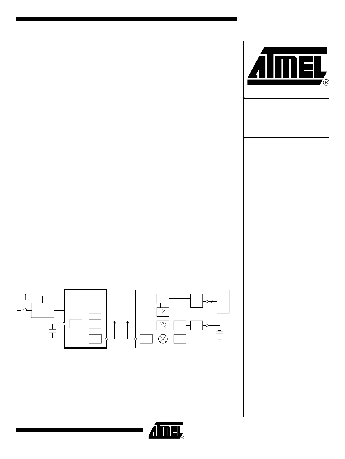
Figure 1. System Block Diagram
UHF ASK/FSK
1 Li cell
Keys
Encoder
ATARx9x
TPM and Remote control
transmitter
ATA5756/
ATA5757
PLL
XTO
VCO
Power
amp.
Antenna Antenna
U3741B/
U3745B/
T5743/
T5744/
LNA VCO
UHF ASK/FSK
Remote control receiver
Demod.
IF Amp
PLL XTO
Control
1...3
µC
Preliminary
Rev. 4702D–RKE–02/04
Page 2
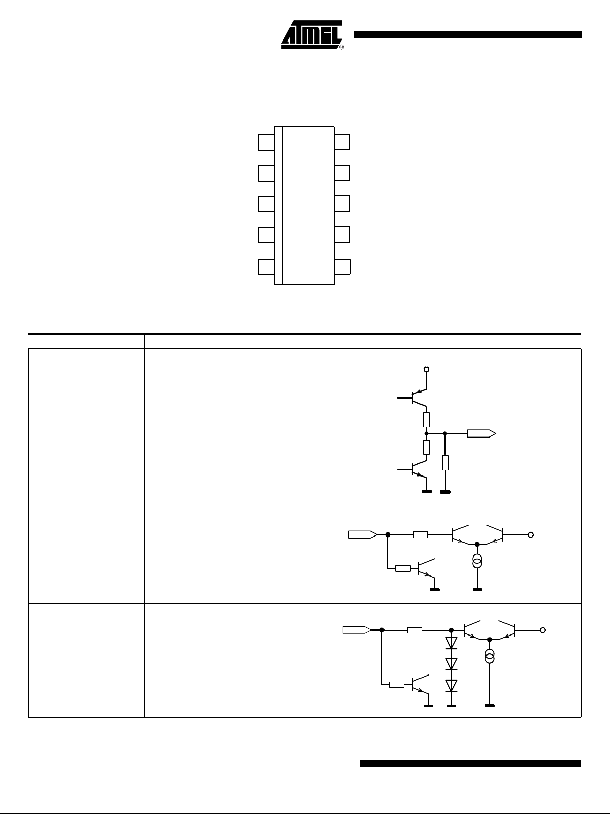
Pin Configuration
Figure 2. Pinning MSOP10
CLK
ASK
FSK
ANT2
1
2
3
4
5ANT1
ATA5756
ATA5757
10
9
8
7
6
ENABLE
GND
VS
XTO1
XTO2
Pin Description
Pin Symbol Function Configuration
Clock output signal for the
microcontroller.
The clock output frequency is set by the
crystal to f
1CLK
The CLK output stays Low in powerdown mode and after enabling of the
PLL.
The CLK output switches on if the
oscillation amplitude of the crystal has
reached a certain level.
XTAL
/8.
VS
100
100
CLK
200k
2ASK
3FSK
2
ATA5756/ATA5757 [Preliminary]
Switches on the power amplifier for
ASK modulation and enables the PLL
and XTO if the ENABLE pin is open
Switches off the FSK switch (switch has
high Z if signal at pin FSK is High) and
enables the PLL and the XTO if the
ENABLE pin is open
ASK
FSK
200k
200k
50k
200k
20 µA
V
= 1.1V
Ref
V
= 1.1V
Ref
5 µA
4702D–RKE–02/04
Page 3
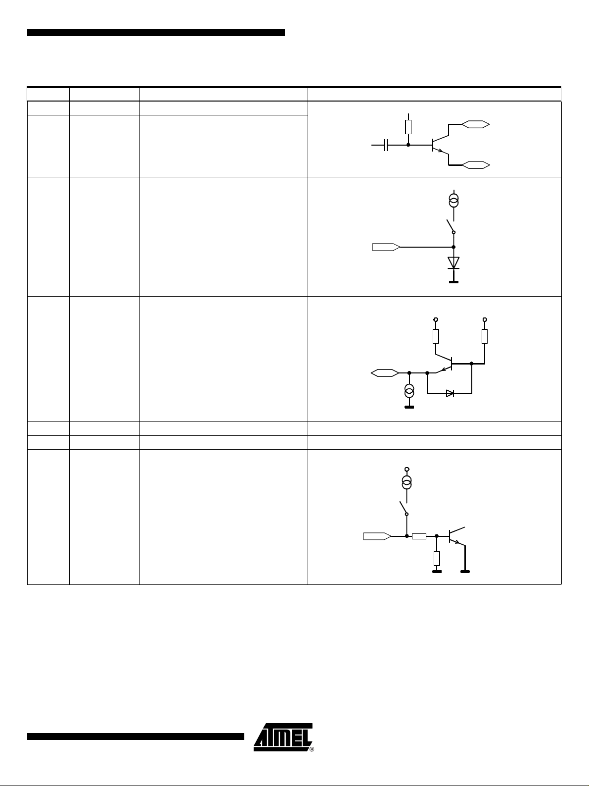
ATA5756/ATA5757 [Preliminary]
Pin Description
Pin Symbol Function Configuration
4 ANT2 Emitter of antenna output stage
5 ANT1 Open collector antenna output
ANT1
ANT2
210 µA
VS
1.2k
6 XTO2 Diode switch, used for FSK modulation
7 XTO1 Connection for crystal
(FSK < 0.25V)
AND
(ENABLE > 1.7V)
XTO2
VS
1.5k
XTO1
182 µA
8 VS Supply voltage See ESD protection circuitry (see Figure 12)
9 GND Ground See ESD protection circuitry (see Figure 12)
VS
ENABLE input
30 µA
10 ENABLE
4702D–RKE–02/04
If ENABLE is connected to GND and
the ASK or FSK pin is High, the device
stays in idle mode.
In normal operation ENABLE is left
open and ASK or FSK is used to enable
the device.
ENABLE
(FSK >1.7 V ) OR
(ASK > 1.7 V)
150k
250k
3
Page 4
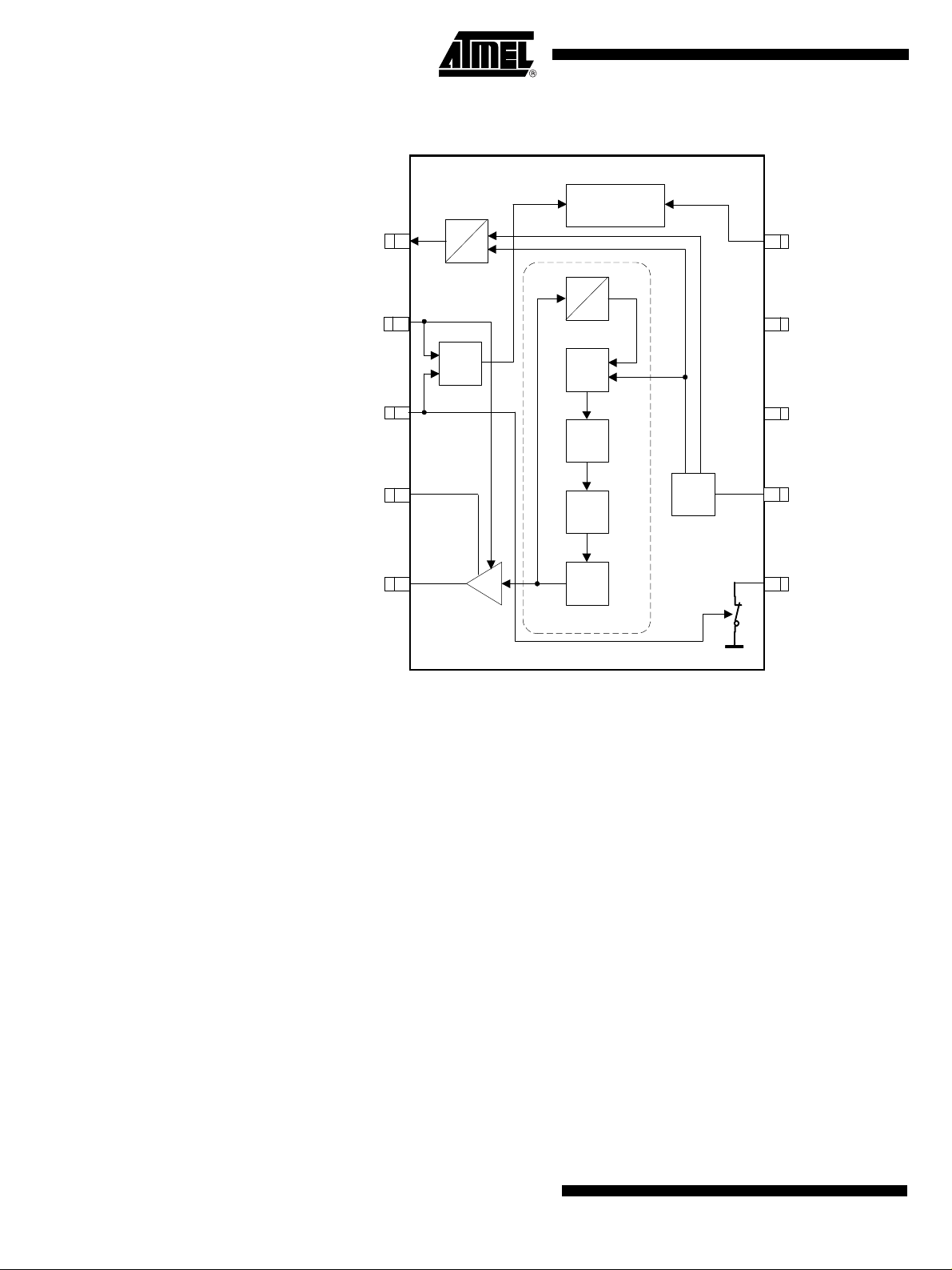
Figure 3. Block Diagram
ATA5756 /
ATA5757
CLK
1
ASK
2
f
Power up/down
EN
8
f
24/
32
ENABLE
10
GND
9
OR
FSK
3
ANT2
4
EN
ANT1
5 6
PA
PLL
PFD
CP
LF
VCO
XTO
VS
8
Ampl. OK
XTO1
7
XTO2
General Description This fully integrated PLL transmitter allows the design of simple, low-cost RF miniature
transmitters for TPM and RKE applications. The VCO is locked to 24 × f
for ATA5756/ATA5757. Thus, a 13.125 MHz/13.56 MHz crystal is needed for a
315 MHz/433.92 MHz transmitter. All other PLL and VCO peripheral elements are
integrated.
XTAL
/32 × f
XTAL
The XTO is a series resonance (current mode) oscillator. Only one capacitor and a
crystal connected in series to GND are needed as external elements in an ASK system.
The internal FSK switch, together with a second capacitor, can be used for FSK
modulation.
The crystal oscillator needs typically 0.6 ms until the CLK output is activated if a crystal
as defined in the electrical characteristics is used (e.g., TPM crystal). For most crystals
used in RKE systems, a shorter time will result.
The CLK output is switched on if the amplitude of the current flowing through the crystal
has reached 35% to 80% of its final value. This is synchronized with the 1.64/1.69 MHz
CLK output. As a result, the first period of the CLK output is always a full period. The
PLL is then locked <250 µs after CLK output activation. This means an additional wait
time of ≥250 µs is necessary before the PA can be switched on and the data transmission can start. This results in a significantly lower time of about 0.85 ms between
enabling the ATA5756/ATA5757 and the beginning of the data transmission which saves
battery power especially in tire pressure monitoring systems.
4
ATA5756/ATA5757 [Preliminary]
4702D–RKE–02/04
Page 5
ATA5756/ATA5757 [Preliminary]
The power amplifier is an open-collector output delivering a current pulse which is nearly
independent from the load impedance and can therefore be controlled via the connected
load impedance.
This output configuration enables a simple matching to any kind of antenna or to 50 Ω. A
high power efficiency for the power amplifier results if an optimized load impedance of
Z
Load, opt
=380Ω + j340 Ω (ATA5756) at 315 MHz and Z
(ATA5757) at 433.92 MHz is used at the 3-V supply voltage.
Load, opt
=280Ω +j310Ω
Functional
Description
If ASK = Low, FSK = Low and ENABLE = open or Low, the circuit is in power-down
mode consuming only a very small amount of current so that a lithium cell used as
power supply can work for many years.
If the ENABLE pin is left open, ENABLE is the logical OR operation of the ASK and FSK
input pins. This means, the IC can be switched on by either the FSK of the ASK input.
If the ENABLE pin is Low and ASK or FSK are High, the IC is in idle mode where the
PLL, XTO and power amplifier are off and the microcontroller ports controlling the ASK
and FSK inputs can be used to control other devices. This can help to save ports on the
microcontroller in systems where other devices with 3-wire interface are used.
With FSK = High and ASK = Low and ENABLE = open or High, the PLL and the XTO
are switched on and the power amplifier is off. When the amplitude of the current
through the crystal has reached 35% to 80% of its final amplitude, the CLK driver is
automatically activated. The CLK output stays Low until the CLK driver has been activated. The driver is activated synchronously with the CLK output frequency, hence, the
first pulse on the CLK output is a complete period. The PLL is then locked within
<250 µs after the CLK driver has been activated, and the transmitter is then ready for
data transmission.
With ASK = High the power amplifier is switched on. This is used to perform the ASK
modulation. During ASK modulation the IC is enabled with the FSK or the ENABLE pin.
With FSK = Low the switch at pin XTO2 is closed, with FSK = High the switch is open.
To achieve a faster start-up of the crystal oscillator, the FSK pin should be High during
start-up of the XTO because the series resistance of the resonator seen from pin XTO1
is lower if the switch is off.
4702D–RKE–02/04
The different modes of the ATA5756/ATA5757 are listed in Table 1, the corresponding
current consumption values can be found in the table “Electrical Characteristics” on
page 15.
Table 1. ATA5756/ATA5757 Modes
ASK Pin FSK Pin ENABLE Pin Mode
Low Low Low/open Power-down mode, FSK switch High Z
Low Low High Power-up, PA off, FSK switch Low Z
Low High High/open Power-up, PA off, FSK switch High Z
High Low High/open Power-up, PA on, FSK switch Low Z
High High High/open Power-up, PA on, FSK switch High Z
Low/High High Low Idle mode, FSK switch High Z
High Low/High Low Idle mode, FSK switch High Z
5
Page 6
Transmission with
ENABLE = open
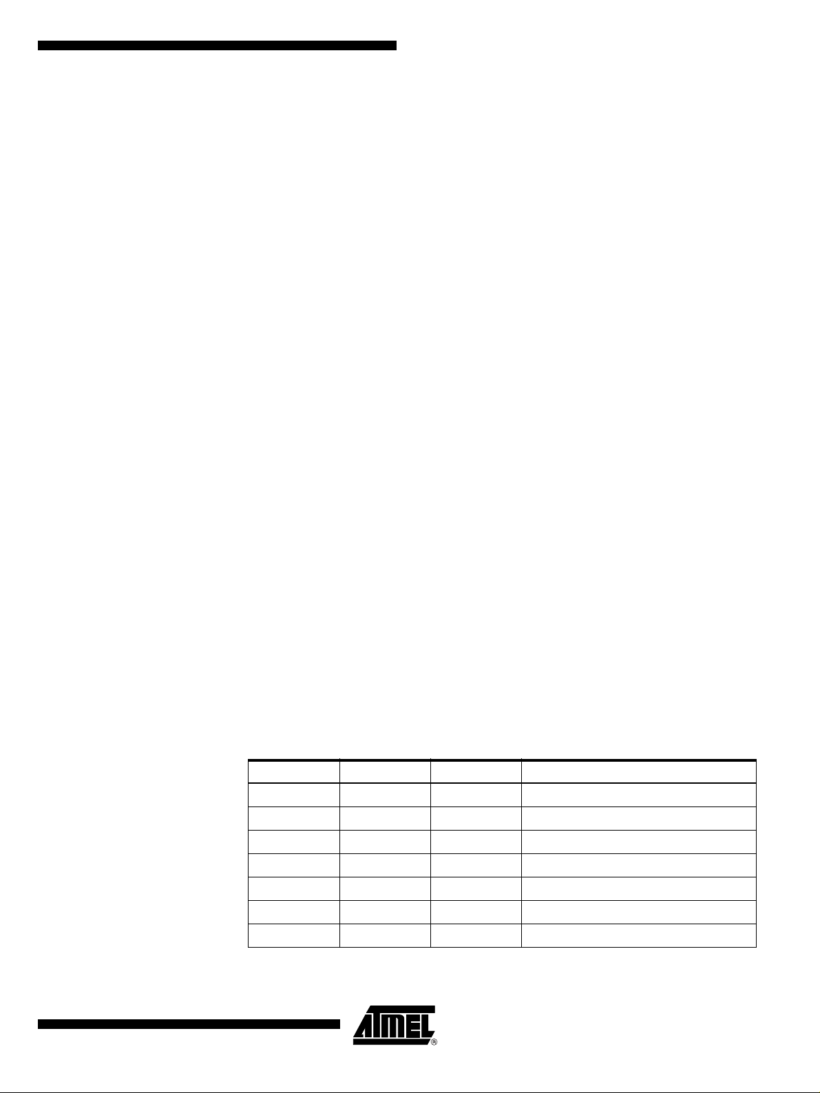
ASK Mode The ATA5756/ATA5757 is activated by ENABLE = open, FSK = High, ASK = Low. The
microcontroller is then switched to external clocking. After typically 0.6 ms, the CLK
driver is activated automatically (i.e., the microcontroller waits until the XTO and CLK
are ready). After another time period of
The output power can then be modulated by means of pin ASK. After transmission, ASK
is switched to Low and the microcontroller returns back to internal clocking. Then, the
ATA5756/ATA5757 is switched to power-down mode with FSK = Low.
Figure 4. Timing ASK Mode with ENABLE not Connected to the Microcontroller
≤250 µs, the PLL is locked and ready to transmit.
FSK
ASK
CLK
Power-down
∆T
XTO
Power-up,
PA off
> 250 µs
Power-up,
PA on
(High)
Power-up,
PA off
(Low)
Power-down
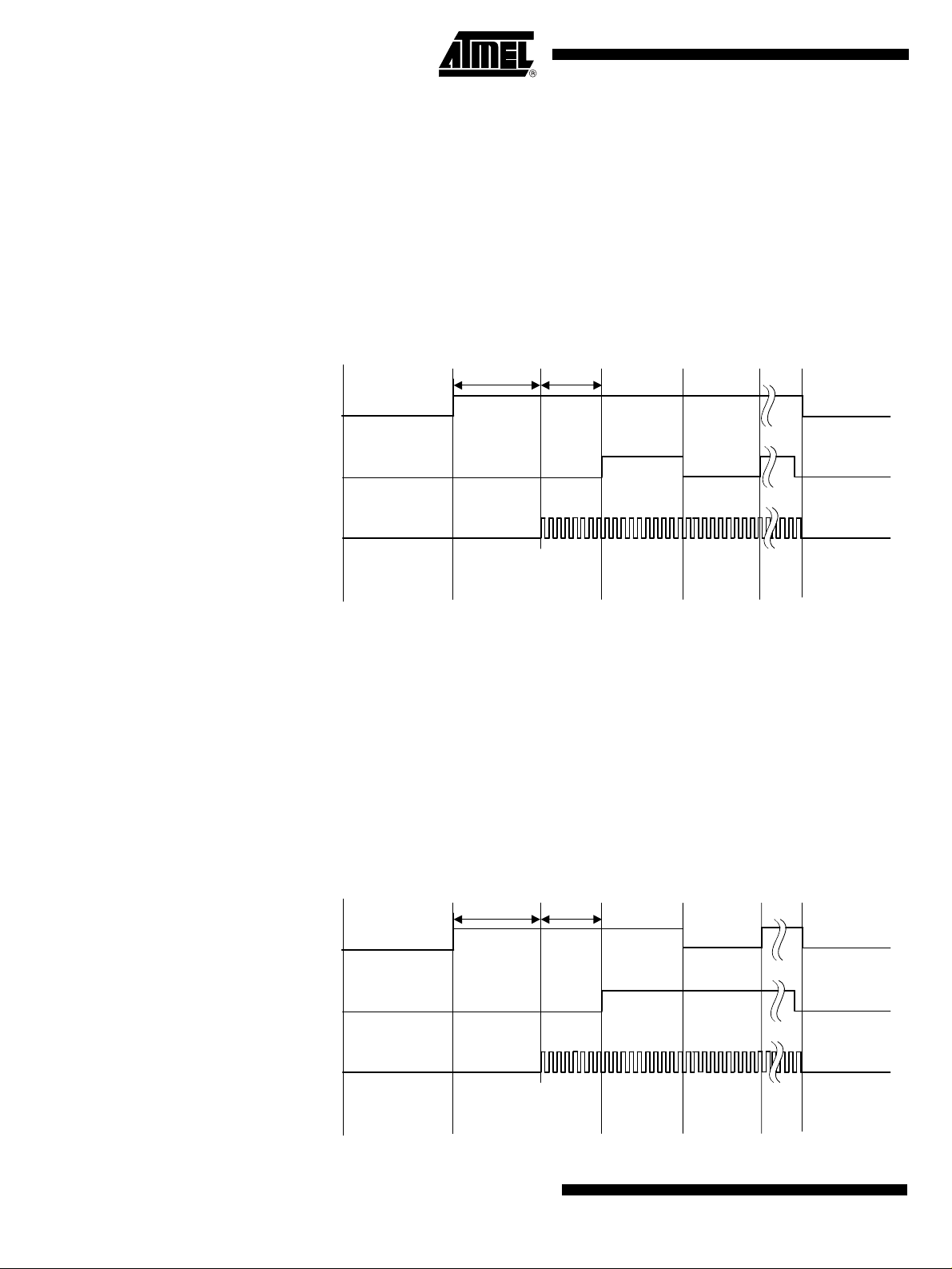
FSK Mode The ATA5756/ATA5757 is activated by FSK = High, ASK = Low. The microcontroller is
then switched to external clocking. After typically 0.6 ms, the CLK driver is activated
automatically (i.e., the microcontroller waits until the XTO and CLK are ready. After
another time period of
≤250 µs, the PLL is locked and ready to transmit. The power
amplifier is switched on with ASK = H. The ATA5756/ATA5757 is then ready for FSK
modulation. The microcontroller starts to switch on and off the capacitor between the
crystal load capacitor and GND by means of pin FSK, thus, changing the reference frequency of the PLL. IF FSK = L the output frequency is lower, if FSK = H output
frequency is higher. After transmission, FSK stays High and ASK is switched to Low and
the microcontroller returns back to internal clocking. Then, the ATA5756/ATA5757 is
switched to power-down mode with FSK = Low.
Figure 5. Timing FSK Mode with ENABLE not Connected to the Microcontroller
∆T
XTO
FSK
ASK
CLK
Power-down
6
ATA5756/ATA5757 [Preliminary]
Power-up,
PA off
> 250 µs
Power-up,
PA on
(f
= High)
RF
Power-up,
PA off
(f
= Low)
RF
Power-down
4702D–RKE–02/04
Page 7

ATA5756/ATA5757 [Preliminary]
Transmission with
ENABLE = High
FSK Mode The ATA5756/ATA5757 is activated by ENABLE = High, FSK = High and ASK = Low.
The microcontroller is then switched to external clocking. After typically 0.6 ms, the CLK
driver is activated automatically (i.e., the microcontroller waits until the XTO and CLK
are ready). After another time period of
The power amplifier is switched on with ASK = H. The ATA5756/ATA5757 is then ready
for FSK modulation. The microcontroller starts to switch on and off the capacitor
between the crystal load capacitor and GND by means of pin FSK, thus, changing the
reference frequency of the PLL. IF FSK = L the output frequency is lower, if FSK = H
output frequency is higher. After transmission, ASK is switched to Low and the microcontroller returns back to internal clocking. Then, the ATA5756/ATA5757 is switched to
power-down mode with ENABLE = Low and FSK = Low.
Figure 6. Timing FSK Mode with ENABLE Connected to the Microcontroller
∆T
XTO
ENABLE
≤250 µs, the PLL is locked and ready to transmit.
> 250 µs
FSK
ASK
CLK
Power-down
Power-up,
PA off
Power-up,
PA on
= High)
(f
RF
Power-up,
PA off
= Low)
(f
RF
Power-down
ASK Mode The ATA5756/ATA5757 is activated by ENABLE = High, FSK = High and ASK = Low.
After activation the microcontroller is switched to external clocking. After typically
0.6 ms, the CLK driver is activated automatically (the microcontroller waits until the XTO
and CLK are ready). After another time period of
≤250 µs, the PLL is locked and ready to
transmit. The output power can then be modulated by means of pin ASK. After transmission, ASK is switched to Low and the microcontroller returns back to internal clocking.
Then, the ATA5756/ATA5757 is switched to power-down mode with ENABLE = Low and
FSK = Low.
4702D–RKE–02/04
7
Page 8

Figure 7. Timing ASK Mode with ENABLE Connected to the Microcontroller
Accuracy of Frequency
Deviation
ENABLE
FSK
ASK
CLK
Power-down
∆T
XTO
> 250 µs
Power-up,
PA off
Power-up,
PA on
(High)
Power-up,
PA off
(Low)
Power-down
The accuracy of the frequency deviation using the XTAL pulling method is about ±20% if
the following tolerances are considered. One important aspect is that the values of C
and CM of typical crystals are strongly correlated which reduces the tolerance of the frequency deviation.
Figure 8. Tolerances of Frequency Modulation
0
~
V
S
C
XTAL
~
CML
Crystal equivalent circuit
R
M
C
S
0
Using a crystal with a motional capacitance of CM= 4.37 fF ±15%, a nominal load
capacitance of C
results in C0= 297 × CM (the correlation has a tolerance of 10%, so C0= 267 to
C
M
326 × C
parasites of C
and C
). If using the internal FSK switch with C
M
= 15 pF ±1% for a nominal frequency deviation of ±19.3 kHz with worst case tol-
5
Stray
= 18 pF and a parallel capacitance of C0= 1.30 pF correlated with
LNOM
Switch
= 0.7 pF ±10%, the resulting C4 and C5 values are C4=10pF ±1%
erances of ±15.8 kHz to ±23.2 kHz.
Stray
C
4
C
5
C
Switch
= 0.9 pF ±20% and estimated
8
ATA5756/ATA5757 [Preliminary]
4702D–RKE–02/04
Page 9

ATA5756/ATA5757 [Preliminary]
Accuracy of the Center
Frequency
The imaginary part of the impedance in large signal steady state oscillation IM
XTO,
seen
into the pin 7 (XTO1), causes some additional frequency tolerances, due to pulling of
the XTO oscillation frequency. These tolerances have to be added to the tolerances of
the crystal itself (adjustment tolerance, temperature stability and ageing) and the influence to the center frequency due to tolerances of C
value of IM
= 110 Ω, C
XTO
Switch
and C
should be absorbed into the C4 and C5 values
Stray
, C5, C
4
by using a crystal with known frequency and choosing C
4
Switch
and C
. The nominal
Stray
and C5, so that the XTO center frequency equals the crystal frequency, and the frequency deviation is as expected.
Then, from the nominal value, the IM
P=-IM
× CM × π × f
XTO
XTO
with f
quency tolerance of P = ±16.86 ppm results. If using crystals with other C
has ±90 Ω tolerances, using the pulling formula
XTO
= 13.56 MHz and CM= 4.4 fF an additional fre-
XTO
M
the
additional frequency tolerance can be calculated in the same way. For example, a lower
= 3.1 fF will reduce the frequency tolerance to 11.87 ppm, where a higher
C
M
= 5.5 fF increases the tolerance to 21.07 ppm.
C
M
CLK Output An output CLK signal of 1.64 MHz (ATA5756 operating at 315 MHz) and 1.69 MHz
(ATA5757 operating at 433.92 MHz) is provided for a connected microcontroller. The
delivered signal is CMOS-compatible with a High and Low time of >125 ns if the load
capacitance is lower than 20 pF. The CLK output is Low in power-down mode due to an
internal pull-down resistor. After enabling the PLL and XTO the signal stays Low until
the amplitude of the crystal oscillator has reached 35% to 80% of its amplitude. Then,
the CLK output is activated synchronously with its output signal so that the first period of
the CLK output signal is a full period.
Clock Pulse Take-over by
Microcontroller
Output Matching and Power
Setting
The clock of the crystal oscillator can be used for clocking the microcontroller. Atmel’s
ATARx9x microcontroller family provides the special feature of starting with an integrated RC oscillator to switch on the ATA5756/ATA5757’s external clocking and to wait
automatically until the CLK output of the ATA5756/ATA5757 is activated. After a time
period of 250 µs the message can be sent with crystal accuracy.
The output power is set by the load impedance of the antenna. The maximum output
power is achieved with a load impedance of Z
315 MHz and Z
is required to deliver the DC current (see Figure 9 on page 10).
to V
S
Load, opt
=280Ω + j310 Ω (ATA5757) at 433.92 MHz. A low resistive path
Load, opt
= 380 Ω+j340Ω (ATA5756) at
The power amplifier delivers a current pulse and the maximum output power is delivered
to a resistive load if the 0.66 pF output capacitance of the power amplifier is compensated by the load impedance.
At the ANT1 pin, the RF output amplitude is about V
- 0.5 V.
S
The load impedance is defined as the impedance seen from the ATA5756’s ANT1,
ANT2 into the matching network. Do not mix up this large-signal load impedance with a
small-signal input impedance delivered as an input characteristic of RF amplifiers.
The latter is measured from the application into the IC instead of from the IC into the
application for a power amplifier.
The 0.66 pF ouput capacitance absorbed into the load impedance a real impedance of
684 Ω (ATA5756) at 315 MHz and 623 Ω (ATA5757) at 433.92 MHz should be mea-
sured with a network analyser at pin 5 (ANT1) with the ATA5756/ATA5757 soldered, an
optimized antenna connected and the power amplifier switched off.
4702D–RKE–02/04
Less output power is achieved by lowering the real parallel part where the parallel imaginary part should be kept constant. Lowering the real part of the load impedance also
reduces the supply voltage dependency of the output power.
9
Page 10

Output power measurement can be done with the circuit as shown in Figure 9. Please
note that the component values must be changed to compensate the individual board
parasitics until the ATA5756/ATA5757 has the right load impedance. Also, the damping
of the cable used to measure the output power must be calibrated.
Figure 9. Output Power Measurement ATA5756/ATA5757
V
S
C1 = 1n
= 68 nH/ 39 nH
L
~
ANT1
ANT2
1
Z = 50Ω
Z
C
Lopt
= 2.2 pF/1.8 pF
2
Power
meter
R
50 Ω
in
~
Table 2 and Table 3 show the output power and the supply current versus temperature
and supply voltage.
Table 2. Output Power and Supply Current versus Temperature and Supply
Voltage for the ATA5756 with Z
Ambient
Temperature
VS = 2.0 V
(dBm/mA)
=380Ω +j340Ω (Correlation Tested)
Load
VS = 3.0 V
(dBm/mA)
VS = 3.6 V
(dBm/mA)
T
= -40°C 3.1 ±1.5 / 7.2 6.1 +2/-3 / 7.7 7.1 +2/-3 / 7.9
amb
T
= +25°C 3.0 ±1.5 / 7.5 6.0 ±2 / 8.1 7.4 ±2 / 8.3
amb
T
= +85°C 3.0 ±1.5 / 7.5 5.8 +2/-3 / 8.2 7.2 +2/-3 / 8.5
amb
T
= +125°C 2.5 ±1.5 / 7.6 5.5 +2/-3 / 8.2 6.5 +2/-3 / 8.5
amb
Table 3. Output Power and Supply Current versus Temperature and Supply
Voltage for the ATA5757 with Z
Ambient
Temperature
T
= -40°C 3.3 ±1.5 / 7.6 6.2 +2/-3 / 8.1 7.1 +2/-3 / 8.4
amb
T
= +25°C 3.0 ±1.5 / 8.0 6.0 ±2 / 8.5 7.5 ±2 / 8.8
amb
T
= +85°C 2.8 ±1.5 / 8.0 5.7 +2/-3 / 8.6 6.8 +2/-3 / 8.8
amb
T
= +125°C 2.7 ±1.5 / 8.1 5.5 +2/-3 / 8.7 6.6 +2/-3 / 8.9
amb
VS = 2.0 V
(dBm/mA)
=280Ω +j310Ω (Correlation Tested)
Load
VS = 3.0 V
(dBm/mA)
VS = 3.6 V
(dBm/mA)
10
ATA5756/ATA5757 [Preliminary]
4702D–RKE–02/04
Page 11

ATA5756/ATA5757 [Preliminary]
Application Circuits For the supply voltage blocking capacitor C
(see Figure 10 on page 12 and Figure 11 on page 13). C
loop antenna to the power amplifier. For C
achieve a better tolerance value and to enable it to realize Z
with standard values.
Together with the pins of ATA5756 and the PCB board wires, C
st
loop that suppresses the 1
harmonic, hence the position of C1 on the PCB is important.
Normally, the best suppression is achieved when C
the pins ANT1 and ANT2.
The loop antenna should not exceed a width of 1.5 mm, otherwise the Q-factor of the
loop antenna is too high.
(50 nH to 100 nH) can be printed on the PCB. C4 should be selected so that the XTO
L
1
runs on the load resonance frequency of the crystal. Normally, a value of 10 pF results
in a 12 pF load-capacitance crystal due to the board parasitic capacitances and the
inductive impedance of the XTO1 pin.
2
, a value of 68 nF/X7R is recommended
3
and C2 are used to match the
1
, two capacitors in series should be used to
by using capacitors
Load,opt
a series resonance
1 forms
is placed as close as possible to
1
4702D–RKE–02/04
11
Page 12

Figure 10. ASK Application Circuit
S1
S2
BPXY
BPXY
BPXY
OSC1
CLK
ASK
ATARx9x
7
ATA5756/ATA5757
1
f
2
VDD
1
VSS
20
BPXY
Power up/down
EN
8
f
24/
32
ENABLE
10
GND
VS
9
Loop
Antenna
C2
C1
VS
L1
OR
FSK
PFD
3
CP
ANT2
4
LF
ANT1
5 6
EN
PA
VCO
PLL
Ampl. OK
XTO
VS
8
XTO1
7
XTO2
C3
VS
XTAL
C4
12
ATA5756/ATA5757 [Preliminary]
4702D–RKE–02/04
Page 13

Figure 11. FSK Application Circuit
ATA5756/ATA5757 [Preliminary]
S1
S2
BPXY
BPXY
BPXY
OSC1
CLK
ASK
ATARx9x
7
ATA5756/ATA5757
1
f
8
2
EN
Power up/down
f
24/
32
VDD
1
VSS
20
BPXY
ENABLE
10
GND
9
VS
Loop
Antenna
C2
C1
VS
L1
OR
FSK
PFD
3
CP
ANT2
4
LF
EN
ANT1
5 6
PA
VCO
PLL
Ampl. OK
XTO
VS
8
XTO1
7
XTO2
C3
VS
XTAL
C5
C4
4702D–RKE–02/04
13
Page 14

Figure 12. ESD Protection Circuit
VS
ANT1
GND
CLK FSK
ASK
ANT2
XTO2
XTO1 ENABLE
Absolute Maximum Ratings
Parameters Symbol Minimum Maximum Unit
Supply voltage V
Power dissipation P
Junction temperature T
Storage temperature T
Ambient temperature T
Ambient temperature in power-down mode for
V
15 minutes without damage with
V
V
< 0.25 V or ENABLE is open,
ENABLE
< 0.25 V, V
ASK
FSK
<0.25V
≤3.2 V
S
T
S
tot
j
stg
amb1
amb2
-55 125 ° C
-55 125 ° C
5V
100 mW
150 °C
175 °C
Thermal Resistance
Parameters Symbol Value Unit
Junction ambient R
14
ATA5756/ATA5757 [Preliminary]
thJA
170 K/W
4702D–RKE–02/04
Page 15

Electrical Characteristics
ATA5756/ATA5757 [Preliminary]
VS = 2.0 V to 3.6 V, T
Typical values are given at V
C
= 4.37 fF, C0= 1.3 pF, C
M
= -40°C to 125°C unless otherwise specified.
amb
= 3.0 V and T
S
= 18 pF, C4= 10 pF, C5= 15 pF and R
LNOM
= 25°C. All parameters are referred to GND (Pin 9).
amb
≤60 Ω
S
Parameters Test Conditions Symbol Min. Typ. Max. Unit
Supply current,
power-down mode
Supply current, idle mode
Supply current, power-up, PA off,
FSK switch High Z
Supply current, power-up, PA on,
FSK switch High Z
Supply current, power-up, PA on,
FSK Low Z
Output power
Output power variation for the full
temperature and supply voltage
range
V
V
T
T
T
V
ASK,FSK can be Low or High
VS≤3.2 V, V
V
VS≤ 3.2 V, C
V
ENABLE is open
ATA5756
ATA5757
VS≤ 3.2 V, C
V
ENABLE is open
ATA5756
ATA5757
VS= 3.0 V, T
f = 315 MHz for
Z
f = 433.92 MHz for
Z
T
V
f
CLK
< 0.25 V or ENABLE is open,
ENABLE
<0.25V, V
ASK
=25°C
amb
=-40°C to +85° C
amb
=-40°C to +125° C
amb
< 0.25 V, VS≤3.2 V
ENABLE
FSK
< 0.25 V ENABLE is open
ASK
CLK
> 1.7 V, V
FSK
CLK
<0.25V, V
FSK
>1.7V,
≤ 10 pF
ASK
≤ 10 pF
ASK
amb
<0.25V
FSK
>1.7V
>1.7V
=25° C,
ATA 57 5 6,
= (380 + j340) Ω
Load, opt
ATA5757,
= (280 + j310) Ω
Load, opt
= -40°C to +125°C,
amb
= 2.0 V to 3.2 V
S
= f
/8
XT0
I
S_Off
I
S_IDLE
I
S
I
S_Transmit1
I
S_Transmit2
P
Out
P
Out
1 100
350
7,000
100 µA
3.6 4.6 mA
8.1
8.5
8.4
8.8
9.8
10.5
10.2
11.0
4 6 8 dBm
1 8 dBm
Load capacitance at pin CLK ≤ 20 pF
Spurious emission
f0 ±f
f0 ±f
CLK
XT0
Spour -42
-60
other spurious are lower
With 50 Ω matching network according
Harmonics
Oscillator frequency XTO
(= phase comparator frequency)
to Figure 9
2nd
3rd
f
= f0/24 ATA5756
XTO
f
= f0/32 ATA5757
XTO
f
= resonant frequency of the
XTAL
XTAL, C
= 4.37 fF, load capacitance
M
selected accordingly
T
= -40°C to +85°C
amb
= -40°C to +125°C
T
amb
∆f
XTO
-14.0
-17.5
-16
-15
f
XTAL
f
XTAL
+14.0
+17.5
nA
nA
nA
mA
mA
mA
mA
dBc
dBc
dBc
ppm
ppm
4702D–RKE–02/04
15
Page 16

Electrical Characteristics (Continued)
VS = 2.0 V to 3.6 V, T
Typical values are given at V
C
= 4.37 fF, C0= 1.3 pF, C
M
= -40°C to 125°C unless otherwise specified.
amb
= 3.0 V and T
S
= 18 pF, C4= 10 pF, C5= 15 pF and R
LNOM
= 25°C. All parameters are referred to GND (Pin 9).
amb
≤60 Ω
S
Parameters Test Conditions Symbol Min. Typ. Max. Unit
Imaginary part of XTO1
Impedance in stady state
oscillation
Real part of XTO1 impedance in
small signal oscillation
Since pulling P is
P = -IM
∆f
XTO
with C
× CM × π × f
XTO
XTO
can be calculated out of IM
=4.37fF
M
This value is important for crystal
oscillator start-up
XTO
IM
RE
XTO
XTO
j20 j110 j200 Ω
-650 -1100 Ω
Time between ENABLE of the IC with
FSK = H and activation of the CLK
output. The CLK is activated
synchronously to the output frequency
Crystal oscillator start-up time
if the current through the XTAL has
reached 35% to 80% of its maximum
∆T
XTO
0.6 1.4 ms
amplitude. Crystal parameters:
= 4.37 fF, C0= 1.3 pF,
C
M
C
= 18 pF, C4= 10 pF,
LNOM
C
= 15 pF, R
5
≤60 Ω
S
Current flowing through the crystal in
XTO drive current
steady state oscillation (peak-to-peak
I
DXTO
300 µApp
value)
Time between the activation of CLK
Locking time of the PLL
and when the PLL is locked
(transmitter ready for data
∆Τ
PLL
250 µs
transmission)
PLL loop bandwidth f
Loop_PLL
In loop phase noise PLL 25 kHz distance to carrier L
Phase noise VCO
Frequency range of VCO
Clock output frequency (CMOS
microcontroller compatible)
Clock output minimum High and
Low time
Series resonance resistance of
the resonator seen from pin
at 1 MHz
at 36 MHz
ATA5756
ATA5757
ATA5756
ATA5757
C
≤ 20 pF, High = 0.8 × Vs,
Load
Low = 0.2 × V
For proper detection of the XTO
amplitude
, f
S
<1.7MHz
CLK
L
T
R
PLL
L
at1M
at36M
f
VCO
f
CLK
CLKLH
s_max
310
432
125 ns
250 kHz
-85 -76 dBc/Hz
-90
-121
-84
-115
dBc/Hz
dBc/Hz
317
448
f0/192
/256
f
0
150 Ω
XTO1
Capacitive load at Pin XTO1 C
L_max
5 pF
This corresponds to 20 kBaud in
FSK modulation frequency rate
Manchester coding and 40 kBaud in
f
MOD_FSK
0 20 kHz
NRZ coding
FSK switch OFF resistance High Z R
FSK switch OFF capacitance High Z capacitance C
FSK switch ON resistance Low Z R
SWIT_OFF
SWIT_OFF
SWIT_ON
50 kΩ
0.75 0.9 1.1 pF
130 175 Ω
Duty cycle of the modulation signal =
ASK modulation frequency rate
50%, this corresponds to 20 kBaud in
Manchester coding and 40 kBaud in
f
MOD_ASK
0 20 kHz
NRZ coding
MHz
MHz
MHz
16
ATA5756/ATA5757 [Preliminary]
4702D–RKE–02/04
Page 17

Electrical Characteristics (Continued)
ATA5756/ATA5757 [Preliminary]
VS = 2.0 V to 3.6 V, T
Typical values are given at V
C
= 4.37 fF, C0= 1.3 pF, C
M
= -40°C to 125°C unless otherwise specified.
amb
= 3.0 V and T
S
= 18 pF, C4= 10 pF, C5= 15 pF and R
LNOM
= 25°C. All parameters are referred to GND (Pin 9).
amb
≤60 Ω
S
Parameters Test Conditions Symbol Min. Typ. Max. Unit
ASK input
FSK input
ENABLE input
Low level input voltage
High level input voltage
Input current high
Low level input voltage
High level input voltage
Input current high
Low level input voltage
High level input voltage
Input current high
Input current Low
V
Il
V
Ih
I
In
V
Il
V
Ih
I
In
V
Il
V
Ih
I
Inh
I
Inl
1.7
1.7
1.7
-40
-40
0.25
30
0.25
30
0.25
40
40
V
V
µA
V
V
µA
V
V
µA
µA
4702D–RKE–02/04
17
Page 18

Ordering Information
Extended Type Number Package Remarks
ATA5756-6DQ MSOP10 –
ATA5757-6DQ MSOP10 –
Package Information MSOP10
18
ATA5756/ATA5757 [Preliminary]
4702D–RKE–02/04
Page 19

Atmel Corporation Atmel Operations
2325 Orchard Parkway
San Jose, CA 95131, USA
Tel: 1(408) 441-0311
Fax: 1(408) 487-2600
Regional Headquarters
Europe
Atmel Sarl
Route des Arsenaux 41
Case Postale 80
CH-1705 Fribourg
Switzerland
Tel: (41) 26-426-5555
Fax: (41) 26-426-5500
Asia
Room 1219
Chinachem Golden Plaza
77 Mody Road Tsimshatsui
East Kowloon
Hong Kong
Tel: (852) 2721-9778
Fax: (852) 2722-1369
Japan
9F, Tonetsu Shinkawa Bldg.
1-24-8 Shinkawa
Chuo-ku, Tokyo 104-0033
Japan
Tel: (81) 3-3523-3551
Fax: (81) 3-3523-7581
Memory
2325 Orchard Parkway
San Jose, CA 95131, USA
Tel: 1(408) 441-0311
Fax: 1(408) 436-4314
Microcontrollers
2325 Orchard Parkway
San Jose, CA 95131, USA
Tel: 1(408) 441-0311
Fax: 1(408) 436-4314
La Chantrerie
BP 70602
44306 Nantes Cedex 3, France
Tel: (33) 2-40-18-18-18
Fax: (33) 2-40-18-19-60
ASIC/ASSP/Smart Cards
Zone Industrielle
13106 Rousset Cedex, France
Tel: (33) 4-42-53-60-00
Fax: (33) 4-42-53-60-01
1150 East Cheyenne Mtn. Blvd.
Colorado Springs, CO 80906, USA
Tel: 1(719) 576-3300
Fax: 1(719) 540-1759
Scottish Enterprise Technology Park
Maxwell Building
East Kilbride G75 0QR, Scotland
Tel: (44) 1355-803-000
Fax: (44) 1355-242-743
RF/Automotive
Theresienstrasse 2
Postfach 3535
74025 Heilbronn, Germany
Tel: (49) 71-31-67-0
Fax: (49) 71-31-67-2340
1150 East Cheyenne Mtn. Blvd.
Colorado Springs, CO 80906, USA
Tel: 1(719) 576-3300
Fax: 1(719) 540-1759
Biometrics/Imaging/Hi-Rel MPU/
High Speed Converters/RF Datacom
Avenue de Rochepleine
BP 123
38521 Saint-Egreve Cedex, France
Tel: (33) 4-76-58-30-00
Fax: (33) 4-76-58-34-80
Literature Requests
www.atmel.com/literature
Disclaimer: Atmel Corporation makes no warranty for the use of its products, other than those expressly contained in the Company’s standard
warranty which is detailed in Atmel’s Terms and Conditions located on the Company’s web site. The Company assumes no responsibility for any
errors which may appear in this document, reserves the right to change devices or specifications detailed herein at any time without notice, and
does not make any commitment to update the information contained herein. No licenses to patents or other intellectual property of Atmel are
granted by the Company in connection with the sale of Atmel products, expressly or by implication. Atmel’s products are not authorized for use
as critical components in life support devices or systems.
© Atmel Corporation 2004. All rights reserved.
®
and combinations thereof are the registered trademarks of Atmel Corporation or its subsidiaries.
Atmel
Other terms and product names may be the trademarks of others.
Printed on recycled paper.
4702D–RKE–02/04
 Loading...