

Page 1

Features
• Transparent RF Receiver ICs for 315 MHz (ATA5746) and 433.92 MHz (ATA5745) With
High Receiving Sensitivity
• Fully Integrated PLL With Low Phase Noise VCO, PLL, and Loop Filter
• High FSK/ASK Sensitivity:–105 dBm (ATA5746, FSK, 9.6 Kbits/s, Manchester, BER 10
–114 dBm (ATA5746, ASK, 2.4 Kbits/s, Manchester, BER 10-3)
–104 dBm (ATA5745, FSK, 9.6 Kbits/s, Manchester, BER 10
–113 dBm (ATA5745, ASK, 2.4 Kbits/s, Manchester, BER 10
• Supply Current: 6.5 mA in Active Mode (3V, 25°C, ASK Mode)
• Data Rate: 1 Kbit/s to 10 Kbits/s Manchester ASK, 1 Kbit/s to 20 Kbits/s Manchester
FSK With Four Programmable Bit Rate Ranges
• Switching Between Modulation Types ASK/FSK and Different Data Rates Possible in
≤1 ms Typically, Without Hardware Modification on Board to Allow Different Modulation
Schemes for RKE, TPMS
• Low Standby Current: 50 µA at 3V, 25°C
• ASK/FSK Receiver Uses a Low-IF Architecture With High Selectivity, Blocking, and
Low Intermodulation (Typical 3-dB Blocking 68.0 dBC at ±3 MHz/74.0 dBC at
±20.0 MHz, System I1dBCP = –31dBm/System IIP3 = –24dBm)
• Telegram Pause Up to 52 ms Supported in ASK Mode
• Wide Bandwidth AGC to Handle Large Out-of-band Blockers above the System I1dBCP
• 440-kHz IF Frequency With 30-dB Image Rejection and 420-kHz IF Bandwidth to
Support PLL Transmitters With Standard Crystals or SAW-based Transmitters
• RSSI (Received Signal Strength Indicator) With Output Signal Dynamic Range of 65 dB
• Low In-band Sensitivity Change of Typically ±2.0 dB Within ±160-kHz Center
Frequency Change in the Complete Temperature and Supply Voltage Range
• Sophisticated Threshold Control and Quasi-peak Detector Circuit in the Data Slicer
• Fast and Stable XTO Start-up Circuit (> –1.4 kΩ Worst-case Start Impedance)
• Clock Generation for Microcontroller
• ESD Protection at all Pins (±4 kV HBM, ±200V MM, ±500V FCDM)
• Dual Supply Voltage Range: 2.7V to 3.3V or 4.5V to 5.5V
• Temperature Range: –40°C to +105°C
• Small 5 mm × 5 mm QFN24 Package
-3
-3
-3
)
)
)
UHF ASK/FSK
Receiver
ATA5745
ATA5746
Preliminary
Applications
• Automotive Keyless Entry and Tire Pressure Monitoring Systems
• Alarm, Telemetering and Energy Metering Systems
Benefits
• Supports Header and Blanking Periods of Protocols Common in RKE and TPM
Systems (Up to 52 ms in ASK Mode)
• All RF Relevant Functions are Integrated. The Single-ended RF Input is Suited for Easy
Adaptation to λ / 4 or Printed-loop Antennas
• Allows a Low-cost Application With Only 8 Passive Components
• Suitable for use in a Receiver for Joint RKE and TPMS
• Optimal Bandwidth Maximizes Sensitivity while Maintaining SAW Transmitter
Compatibility
• Clock Output Provides an External Microcontroller Crystal-precision Time Reference
• Well Suited for Use With PLL Transmitter ATA5756/ATA5757
4596A–RKE–05/06
Page 2
1. General Description
The ATA5745/ATA5746 is a UHF ASK/FSK transparent receiver IC with low power consumption
supplied in a small QFN24 package (body 5 mm × 5 mm, pitch 0.65 mm). ATA5745 is used in
the 433 MHz to 435 MHz band of operation, and ATA5746 in 313 MHz to 317 MHz. The IC combines the functionality of remote keyless entry (RKE - typically low bit rate ASK) and tire
pressure monitoring (TPM - typically high bit rate FSK) into one receiver under the control of an
external microcontroller such as an ATmega48 (AVR
For improved image rejection and selectivity, the IF frequency is fixed to 440 kHz. The IF block
uses an 8th-order band pass yielding a receive bandwidth of 420 kHz. This enables the use of
the receiver in both SAW- and PLL-based transmitter systems utilizing various types of data-bit
encoding such as pulse width modulation, Manchester modulation, variable pulse modulation,
pulse position modulation, and NRZ. Prevailing encryption protocols such as Keeloq
supported due to the receiver’s ability to hold the current data slicer threshold for up to 52 ms
when incoming RF telegrams contain a blanking interval. This feature eliminates erroneous
noise from appearing on the demodulated data output pin, and simplifies software decoding
algorithms. The decoding of the data stream must be carried out by a connected microcontroller
device. Because of the highly integrated design, the only required RF components are for the
purpose of receiver antenna matching.
ATA5745 and ATA5746 support Manchester bit rates of 1 Kbit/s to 10 Kbits/s in ASK and 1 Kbit/s
to 20 Kbits/s in FSK mode. The four discrete bit rate passbands are selectable and cover
1.0 Kbit/s to 2.5 Kbits/s, 2.0 Kbits/s to 5.0 Kbits/s, 4.0 Kbits/s to 10.0 Kbits/s, and 8.0 Kbits/s to
10.0 Kbits/s or 20.0 Kbits/s (for ASK or FSK, respectively). The receiver contains an RSSI output
to provide an indication of received signal strength and a SENSE input to allow the customer to
select a threshold below which the DATA signal is gated off. ASK/FSK and bit rate ranges are
selected by the connected microcontroller device via pins ASK_NFSK, BR0, and BR1.
®
).
®
are easily
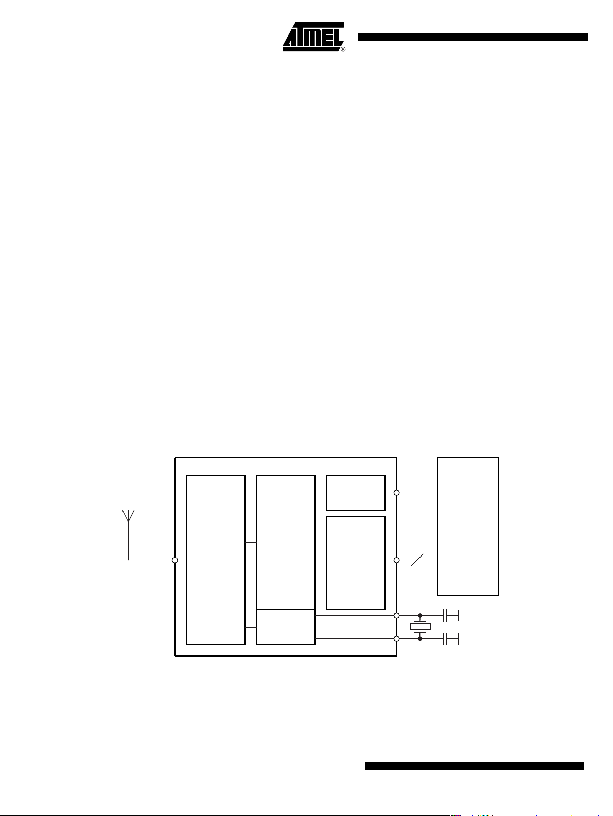
Figure 1-1. System Block Diagram
Antenna
RF Receiver
(LNA, Mixer,
Demodulator)
VCO, PLL,
IF Filter,
RSSI Amp.,
ATA5745/ATA5746
Digital Control
Logic
XTO
Powe r
Supply
Microcontroller
4 ... 8
Microcontroller
Interface
2
ATA5745/ATA5746 [Preliminary]
4596A–RKE–05/06
Page 3
Figure 1-2. Pinning QFN24
ATA5745/ATA5746 [Preliminary]
TEST2
TEST1
CLK_OUT
CLK_OUT_CTRL1
CLK_OUT_CTRL0
ENABLE
DATA_OUT
24
1
2
3
4
5
6
789101112
XTAL2
CDEM
23 22
XTAL1
BR1RXBR0
ASK_NFSK
21 20 19
VS5V
DVCC
S3V_AVCC
TEST3
18
RSSI
17
SENSE_CTRL
16
SENSE
15
14
LNA_IN
LNA_GND
13
GND
Table 1-1. Pin Description
Pin Symbol Function
1 TEST2 Test pin, during operation at GND
2 TEST1 Test pin, during operation at GND
3 CLK_OUT Output to clock a connected microcontroller
4 CLK_OUT_CTRL1 Input to control CLK_OUT (MSB)
5 CLK_OUT_CTRL0 Input to control CLK_OUT (LSB)
6 ENABLE Input to enable the XTO
7 XTAL2 Reference crystal
8 XTAL1 Reference crystal
9 DVCC Digital voltage supply blocking
10 VS5V Power supply input for voltage range 4.5V to 5.5V
11 VS3V_AVCC Power supply input for voltage range 2.7V to 3.3V
12 GND Ground
13 LNA_GND RF ground
14 LNA_IN RF input
15 SENSE Sensitivity control resistor
16 SENSE_CTRL
17 RSSI Output of the RSSI amplifier
18 TEST3 Test pin, during operation at GND
19 RX Input to activate the receiver
20 BR0 Bit rate selection, LSB
21 BR1 Bit rate selection, MSB
22 ASK_NFSK
23 CDEM Capacitor to adjust the lower cut-off frequency data filter
24 DATA_OUT Data output
GND Ground/backplane (exposed die pad)
Sensitivity selection
Low: Normal sensitivity, High: Reduced sensitivity
FSK/ASK selection
Low: FSK, High: ASK
4596A–RKE–05/06
3
Page 4
Figure 1-3. Block Diagram
CDEM
SENSE
SENSE_CTRL
GND
DVCC
LNA_IN
LNA_GND
ASK/FSK
Demo-
dulator
IF Amp
IF Filter
LPF
IF Amp
LPF
LNA VCO
ASK
FSK
PLL
(/24, /32)
Power
Supply
ASK/FSK
Control
Data
Slicer
Standby
Logic Control
XTO
Div. by 3, 6, 12
XTO
VS3V_AVCC
VS5V
ASK_NFSK
DATA_OUT
BR0
BR1
RX
CLK_OUT_CTRL1
CLK_OUT_CTRL0
CLK_OUT
RSSI
ENABLE
TEST1
TEST2
TEST3
XTAL2 XTAL1
4
ATA5745/ATA5746 [Preliminary]
4596A–RKE–05/06
Page 5

2. RF Receiver
As seen in Figure 1-3 on page 4, the RF receiver consists of a low-noise amplifier (LNA), a local
oscillator, and the signal processing part with mixer, IF filter, IF amplifier with analog RSSI,
FSK/ASK demodulator, data filter, and data slicer.
In receive mode, the LNA pre-amplifies the received signal which is converted down to a
440-kHz intermediate frequency (IF), then filtered and amplified before it is fed into an FSK/ASK
demodulator, data filter, and data slicer. The received signal strength indicator (RSSI) signal is
available at the pin RSSI.
2.1 Low-IF Receiver
The receive path consists of a fully integrated low-IF receiver. It fulfills the sensitivity, blocking,
selectivity, supply voltage, and supply current specification needed to design an automotive integrated receiver for RKE and TPM systems. A benefit of the integrated receive filter is that no
external components needed.
At 315 MHz, the ATA5745 receiver (433.92 MHz for the ATA5746 receiver) has a typical system
noise figure of 6.0 dB (7.0 dB), a system I1dBCP of –31 dBm (–30 dBm), and a system IIP3 of
–24 dBm (–23 dBm). The signal path is linear for out-of-band disturbers up to the I1dBCP and
hence there is no AGC or switching of the LNA needed, and a better blocking performance is
achieved. This receiver uses an IF (intermediate frequency) of 440 kHz, the typical image rejection is 30 dB and the typical 3-dB IF filter bandwidth is 420 kHz (f
f
10 Kbits/s Manchester with ±38 kHz frequency deviation in FSK mode, thus, the resulting sensitivity at 315 MHz (433.92 MHz) is typically –105 dBm (–104 dBm).
= 230 kHz and f
lo_IF
ATA5745/ATA5746 [Preliminary]
= 440 kHz ± 210 kHz,
IF
= 650 kHz). The demodulator needs a signal-to-noise ratio of 8.5 dB for
hi_IF
Due to the low phase noise and spurs of the synthesizer together with the 8th-order integrated IF
filter, the receiver has a better selectivity and blocking performance than more complex double
superhet receivers, without using external components and without numerous spurious receiving frequencies.
A low-IF architecture is also less sensitive to second-order intermodulation (IIP2) than direct
conversion receivers where every pulse or amplitude modulated signal (especially the signals
from TDMA systems like GSM) demodulates to the receiving signal band at second-order
non-linearities.
4596A–RKE–05/06
5
Page 6
2.2 Input Matching at LNA_IN
The measured input impedances as well as the values of a parallel equivalent circuit of these
impedances can be seen in Table 2-1. The highest sensitivity is achieved with power matching
of these impedances to the source impedance.
Table 2-1. Measured Input Impedances of the LNA_IN Pin
fRF [MHz] ZIn(RF_IN) [Ω]R
433.92 (55 – j216) 900Ω//1.60
The matching of the LNA input to 50Ω is done using the circuit shown in Figure 2-1 and the val-
ues of the matching elements given in Table 2-2. The reflection coefficients were always
≤ –10 dB. Note that value changes of C1 and L1 may be necessary to compensate individual
board layout parasitics. The measured typical FSK and ASK Manchester-code sensitivities with
a bit error rate (BER) of 10
ments were done with wire-wound inductors having quality factors reported in Table 2-2,
resulting in estimated matching losses of 0.8 dB at 315 MHz and 433.92 MHz. These losses can
be estimated when calculating the parallel equivalent resistance of the inductor with
R
=2×π×f × L × QL and the matching loss with 10 log(1+R
loss
Figure 2-1. Input Matching to 50Ω
//C
In_p
[pF]
In_p
315 (72.4 – j298) 1300Ω//1.60
–3
are shown in Table 2-3 and Table 2-4 on page 7. These measure-
In_p/Rloss
).
RF
IN
Table 2-2. Input Matching to 50Ω
fRF [MHz] C1 [pF] L1 [nH] Q
315 2.2 68 20
433.92 2.2 36 15
C1
L1
ATA5745/ATA5746
14
LNA_IN
L1
6
ATA5745/ATA5746 [Preliminary]
4596A–RKE–05/06
Page 7
ATA5745/ATA5746 [Preliminary]
Table 2-3. Measured Typical Sensitivity FSK, ±38 kHz, Manchester, BER = 10
BR_Range_0
RF Frequency
315 MHz –108 dBm –108 dBm –107 dBm –105 dBm –104 dBm –104 dBm
433.92 MHz –107 dBm –107 dBm –106 dBm –104 dBm –103 dBm –103 dBm
1.0 Kbit/s
BR_Range_0
2.5 Kbits/s
BR_Range_1
5 Kbits/s
BR_Range_2
10 Kbits/s
Table 2-4. Measured Typical Sensitivity 100% ASK, Manchester, BER = 10
BR_Range_0
RF Frequency
315 MHz –114 dBm –114 dBm –113 dBm –111 dBm –109 dBm
433.92 MHz –113 dBm –113 dBm –112 dBm –110 dBm –108 dBm
1.0 Kbit/s
BR_Range_0
2.5 Kbits/s
BR_Range_1
5 Kbits/s
BR_Range_2
10 Kbits/s
–3
BR_Range_3
10 Kbits/s
–3
BR_Range_3
10 Kbits/s
BR_Range_3
20 Kbits/s
Conditions for the sensitivity measurement:
The given sensitivity values are valid for Manchester-modulated signals. For the sensitivity measurement the distance from edge to edge must be evaluated. As can be seen in Figure 6-1 on
page 24, in a Manchester-modulated data stream, the time segments T
To reach the specified sensitivity for the evaluation of T
following limits should be used (T
min, TEE max, 2 × TEE min, 2 × TEE max).
EE
and 2 × TEE in the data stream, the
EE
and 2 × TEE occur.
EE
Table 2-5. Limits for Sensitivity Measurements
Bit Rate TEE Min TEE Typ TEE Max 2 × TEE Min 2 × TEE Typ 2 × TEE Max
1.0 Kbit/s 260 µs 500 µs 790 µs 800 µs 1000 µs 1340 µs
2.4 Kbits/s 110 µs 208 µs 310 µs 320 µs 416 µs 525 µs
5.0 Kbits/s 55 µs 100 µs 155 µs 160 µs 200 µs 260 µs
9.6 Kbits/s 27 µs 52 µs 78 µs 81 µs 104 µs 131 µs
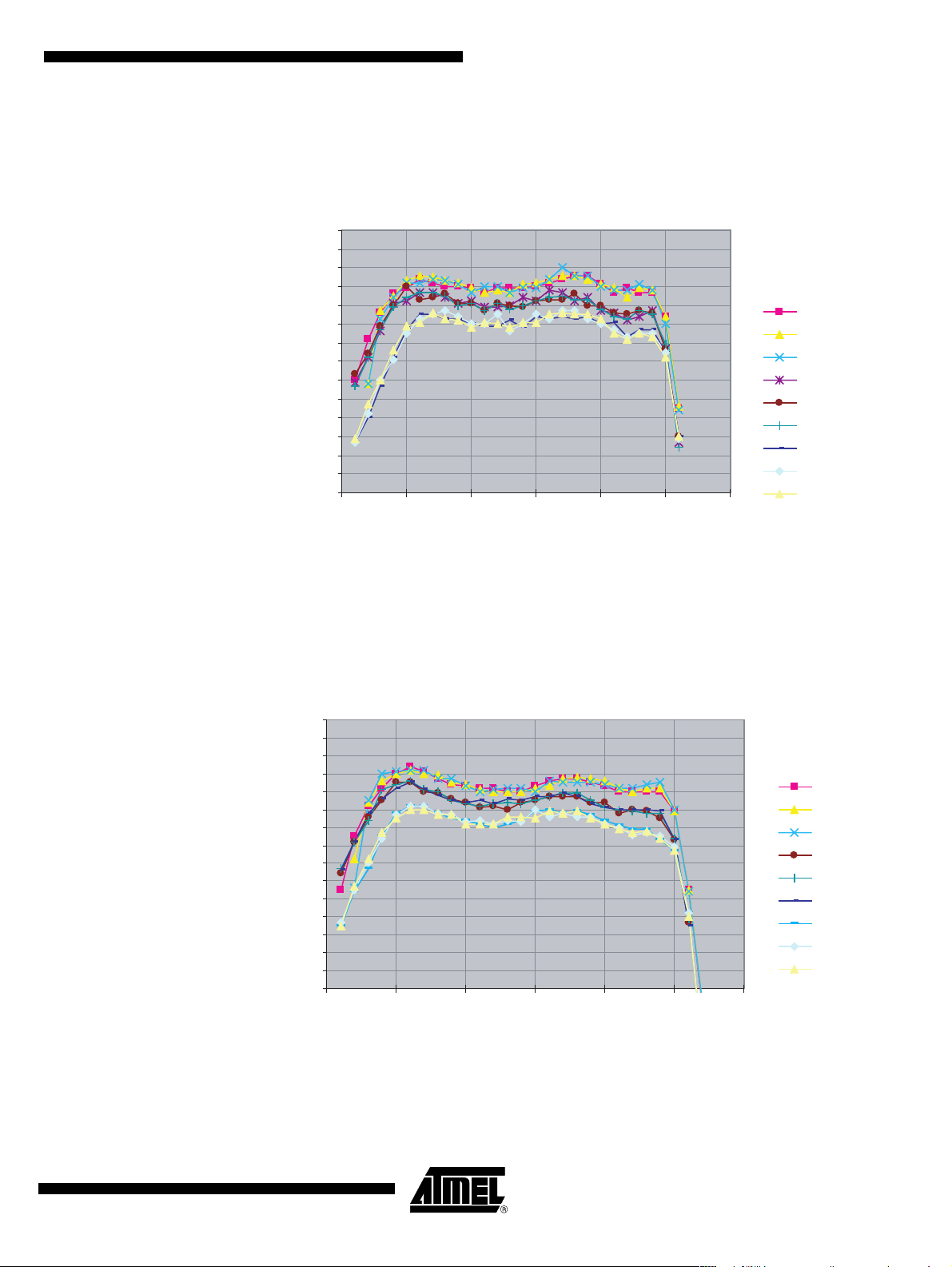
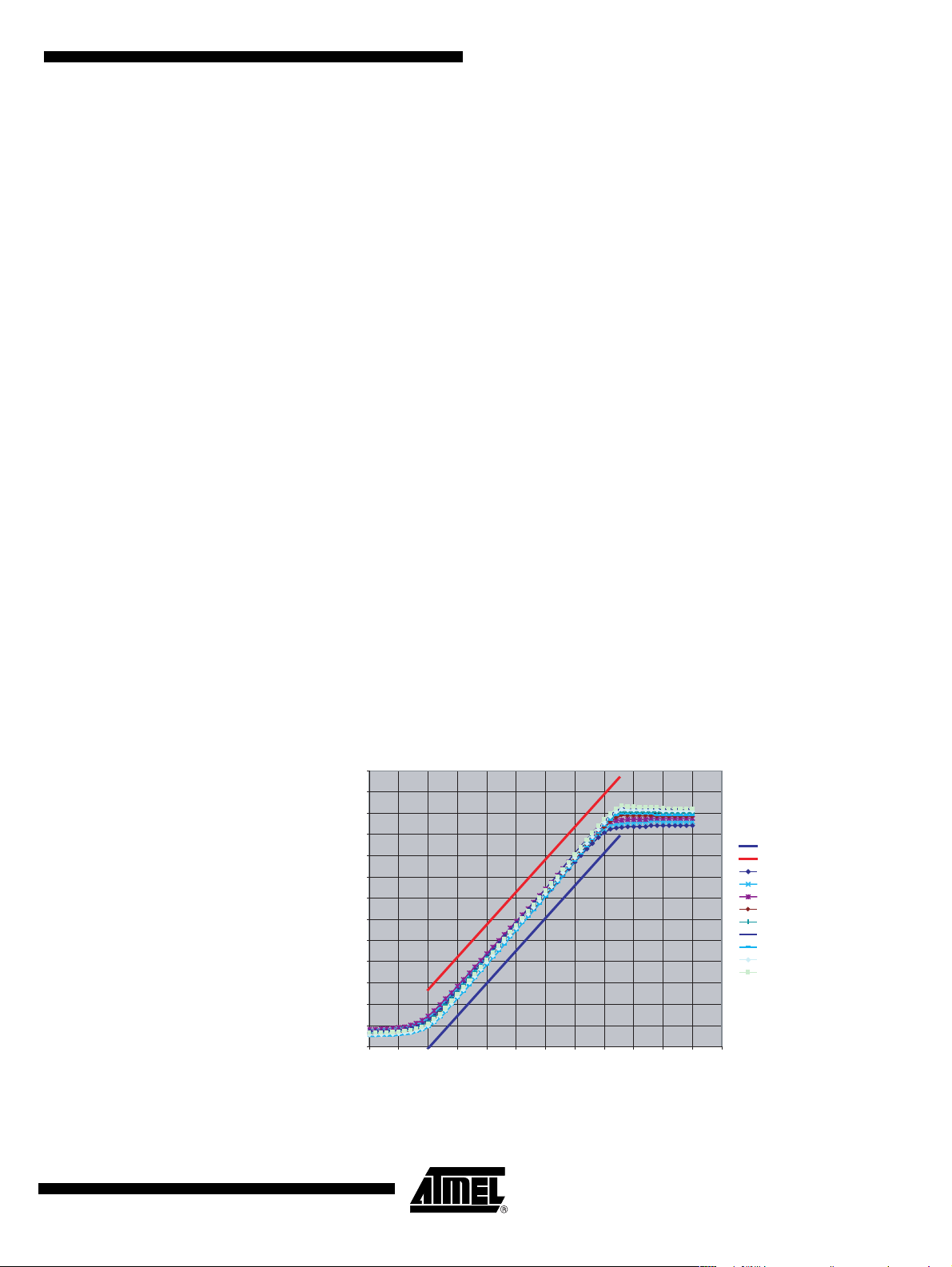
2.3 Sensitivity Versus Supply Voltage, Temperature and Frequency Offset
To calculate the behavior of a transmission system, it is important to know the reduction of the
sensitivity due to several influences. The most important are frequency offset due to crystal
oscillator (XTO) and crystal frequency (XTAL) errors, temperature and supply voltage dependency of the noise figure, and IF-filter bandwidth of the receiver. Figure 2-2 and Figure 2-3 on
page 8 show the typical sensitivity at 315 MHz, ASK, 2.4 Kbits/s and 9.6 Kbits/s, Manchester,
Figure 2-4 and Figure 2-5 on page 9 show a typical sensitivity at 315 MHz, FSK, 2.4 Kbits/s and
9.6 Kbits/s, ±38 kHz, Manchester versus the frequency offset between transmitter and receiver
at T
3.0V and 3.3V.
= –40°C, +25°C, and +105°C and supply voltage VS = VS3V_AVCC = VS5V = 2.7V,
amb
4596A–RKE–05/06
7
Page 8

Figure 2-2. Measured Sensitivity (315 MHz, ASK, 2.4 Kbits/s, Manchester) Versus Fre-
(
quency Offset
Input Sensitivity (dBm) at BER < 1e-3, ATA5746, ASK, 2.4 Kbits/s (Manchester),
BR = 0
-118.00
-117.00
-116.00
-115.00
-114.00
-113.00
-112.00
-111.00
-110.00
-109.00
-108.00
-107.00
Input Sensitivity (dBm)
-106.00
-105.00
-104.00
-103.00
-300 -200 -100 0 100 200 300
delta RF (k Hz) at 315 MHz
2.7V / -40˚C
3.0V / -40˚C
3.3V / -40˚C
2.7V / 27˚C
3.0V / 27˚C
3.3V / 27˚C
2.7V / 105˚C
3.0V / 105˚C
3.3V / 105˚C
Figure 2-3. Measured Sensitivity (315 MHz, ASK, 9.6 Kbits/s, Manchester) Versus Fre-
quency Offset
Input Sensitivity (dBm) at BER < 1e-3, ATA5746, ASK, 9.6 Kbits/s (Manchester),
BR = 2
-115.00
-114.00
-113.00
-112.00
-111.00
-110.00
-109.00
-108.00
-107.00
-106.00
-105.00
Input Sensitivity (dBm)
-104.00
-103.00
-102.00
-101.00
-100.00
-300 -200 -100 0 100 200 300
2.7V / -40˚C
3.0V / -40˚C
3.3V / -40˚C
2.7V / 27˚C
3.0V / 27˚C
3.3V / 27˚C
2.7V / 105˚C
3.0V / 105˚C
3.3V / 105˚C
delta RF
8
ATA5745/ATA5746 [Preliminary]
kHz) at 315 MHz
4596A–RKE–05/06
Page 9
ATA5745/ATA5746 [Preliminary]
C
C
C
Figure 2-4. Measured Sensitivity (315 MHz, FSK, 2.4 Kbits/s, ±38 kHz, Manchester) Versus
Frequency Offset
Input Sensitivity (dBm) at BER < 1e-3, ATA5746, FSK, 2.4 Kbits/s
(Manchester), BR0
-112.00
-111.00
-110.00
-109.00
-108.00
-107.00
-106.00
-105.00
-104.00
-103.00
-102.00
Input Sensitivity (dBm)
-101.00
-100.00
-99.00
-98.00
-300 -200 -100 0 100 200 300
2.7V / -40˚C
3.0V / -40˚C
3.3V / -40˚C
2.7V / 27˚C
3.0V / 27˚C
3.3V / 27˚C
2.7V / 105˚C
3.0V / 105˚C
3.3V / 105˚C
delta RF (k Hz) at 315 MHz
Figure 2-5. Measured Sensitivity (315 MHz, FSK, 9.6 Kbits/s, ±38 kHz, Manchester) Versus
Frequency Offset
Input Sensitivity (dBm) at BER < 1e-3, ATA5746, FSK, 9.6 Kbits/s (Manchester),
BR = 2
-110.00
-109.00
-108.00
-107.00
-106.00
-105.00
-104.00
-103.00
-102.00
-101.00
-100.00
-99.00
Input Sensitivity (dBm)
-98.00
-97.00
-96.00
-95.00
-300 -200 -100 0 100 200 300
2.7V / -40˚C
3.0V / -40˚C
3.3V / -40˚C
2.7V / 27˚C
3.0V / 27˚C
3.3V / 27˚C
2.7V / 105˚
3.0V / 105˚
3.3V / 105˚
4596A–RKE–05/06
delta RF (k Hz) at 315 MHz
9
Page 10

As can be seen in Figure 2-5 on page 9, the supply voltage has almost no influence. The temperature has an influence of about ±1.0 dB, and a frequency offset of ±160 kHz also influences
by about ±1 dB. All these influences, combined with the sensitivity of a typical IC (–105 dB), are
then within a range of –103.0 dBm and –107.0 dBm over temperature, supply voltage, and frequency offset. The integrated IF filter has an additional production tolerance of ±10 kHz, hence,
a frequency offset between the receiver and the transmitter of ±160 kHz can be accepted for
XTAL and XTO tolerances.
Note: For the demodulator used in the ATA5745/ATA5746, the tolerable frequency offset does not
change with the data frequency. Hence, the value of ±160 kHz is valid for 1 Kbit/s to 10 Kbits/s.
This small sensitivity change over supply voltage, frequency offset, and temperature is very
unusual in such a receiver. It is achieved by an internal, very fast, and automatic frequency correction in the FSK demodulator after the IF filter, which leads to a higher system margin. This
frequency correction tracks the input frequency very quickly. If, however, the input frequency
makes a larger step (for example, if the system changes between different communication partners), the receiver has to be restarted. This can be done by switching back to Standby mode
and then again to Active mode (pin RX 1
ASK_NFSK (0
→1 → 0).
→ 0 → 1) or by generating a positive pulse on pin
2.4 Frequency Accuracy of the Crystals in a Combined RKE and TPM System
In a tire pressure measurement system working at 315 MHz and using an ATA5756 as transmitter and an ATA5746 is receiver, the higher frequency tolerances and the tolerance of the
frequency deviation of the transmitter has to be considered.
In the TPM transmitter, the crystal has a frequency error over temperature –40°C to 125°C,
aging, and tolerance of ±80 ppm (±25.2 kHz at 315 MHz). The tolerances of the XTO, the
capacitors used for FSK modulation, and the stray capacitances cause an additional frequency
error of ±30 ppm (±9.45 kHz at 315 MHz). The frequency deviation of such a transmitter varies
between ±16 kHz and ±24 kHz, since a higher frequency deviation is equivalent to a frequency
error this has to be considered as an additional ±24 kHz – ±19.5 kHz = ±4.5kHz frequency tolerance (19.5 kHz is constant). All tolerances added, these transmitters have a worst-case
frequency offset of ±39.15 kHz.
For the receiver in the car, a tolerance of ±160 kHz – ±39.15 kHz = ±120.85 kHz (±383.6 ppm)
remains. The needed frequency stability of the crystals over temperature and aging is
±383.6 ppm – ±5 ppm = ±378.6 ppm. The aging of such a crystal is ±10 ppm, leaving a reasonable ±368.6 ppm for the temperature dependency of the crystal frequency in the car.
Since the receiver in the car is able to receive these TPM transmitter signals with high frequency
offsets, the component specification in the key can be largely relaxed.
This system calculation is based on worst-case tolerances of all the components; this leads in
practice to a system with margin.
For a 433.92 MHz TPM system using ATA5757 as transmitter and ATA5745 as receiver, the
same calculation must be done, but since the RF frequency is higher, every ppm of crystal tolerances results in higher frequency offset and either the system must have lower tolerances or a
lower margin at this frequency.
10
ATA5745/ATA5746 [Preliminary]
4596A–RKE–05/06
Page 11
ATA5745/ATA5746 [Preliminary]
0
)
2.5 RX Supply Current Versus Temperature and Supply Voltage
Table 2-7 shows the typical supply current of the receiver in Active mode versus supply voltage
and temperature with VS = VS3V_AVCC = VS5V.
Table 2-6. Measured Current in Active Mode ASK
VS = VS3V_AVCC = VS5V 2.7V 3.0V 3.3V
T
= –40°C 5.4 mA 5.5 mA 5.6 mA
amb
T
= 25°C 6.4 mA 6.5 mA 6.6 mA
amb
T
= 105°C 7.4 mA 7.5 mA 7.6 mA
amb
Table 2-7. Measured Current in Active Mode FSK
VS = VS3V_AVCC = VS5V 2.7V 3.0V 3.3V
T
= –40°C 5.6 mA 5.7 mA 5.8 mA
amb
T
= 25°C 6.6 mA 6.7 mA 6.8 mA
amb
T
= 105°C 7.6 mA 7.7 mA 7.8 mA
amb
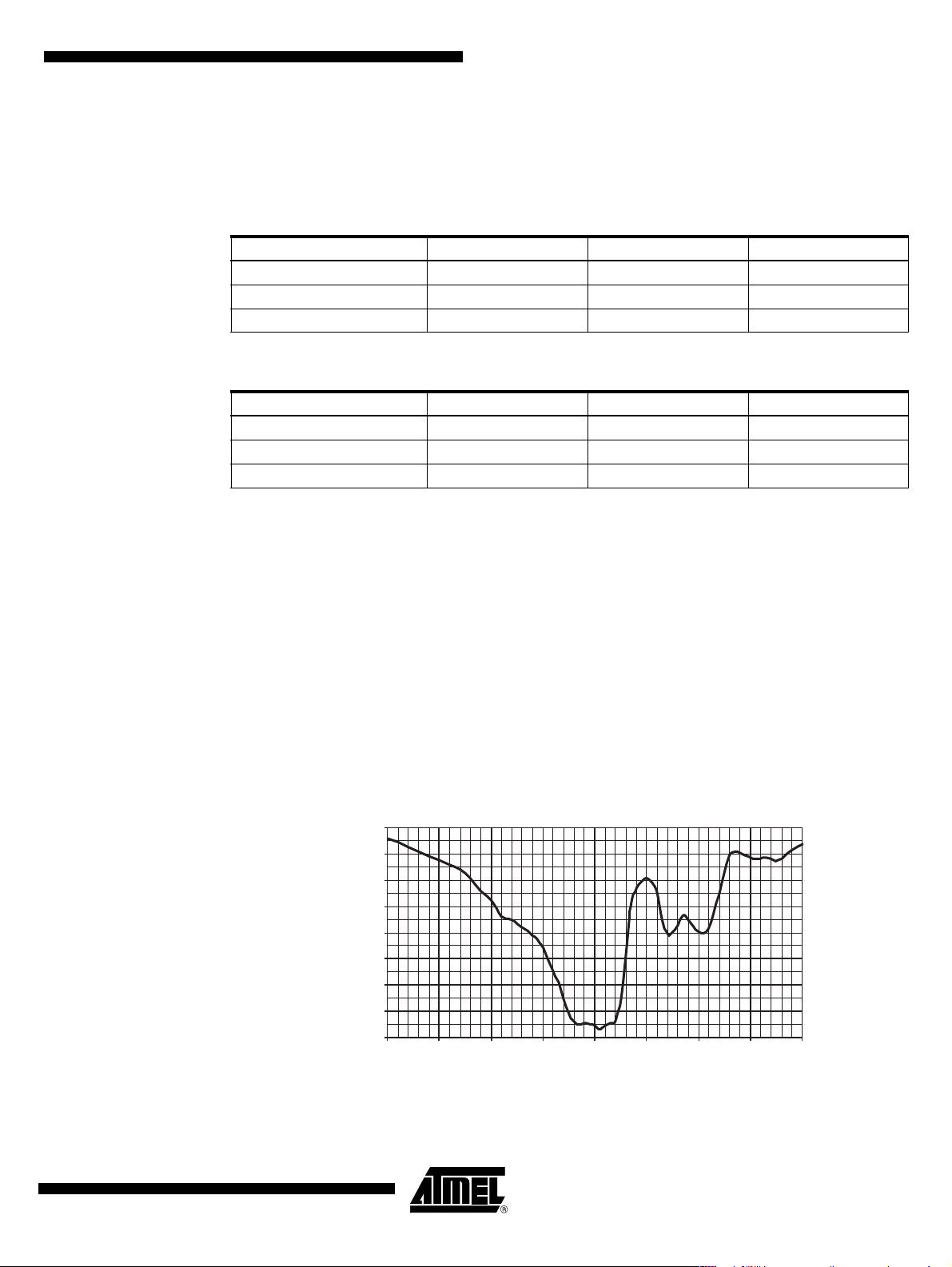
2.6 Blocking, Selectivity
As can be seen in Figure 2-6 on page 11, and Figure 2-7 and Figure 2-8 on page 12, the
receiver can receive signals 3 dB higher than the sensitivity level in the presence of large blockers of –34.5 dBm or –28 dBm with small frequency offsets of ±3 MHz or ±20 MHz.
Figure 2-6, and Figure 2-7 on page 12 show the narrow-band blocking, and Figure 2-8 on page
12 shows the wide-band blocking characteristic. The measurements were done with a useful
signal of 315 MHz, FSK, 10 Kbits/s, ±38 kHz, Manchester, BR_Range2 with a level of
–105 dBm + 3 dB = –102 dBm, which is 3 dB above the sensitivity level. The figures show how
much larger than –102 dBm a continuous wave signal can be, until the BER is higher than 10
–3
The measurements were done at the 50Ω input shown in Figure 2-1 on page 6. At 3 MHz, for
example, the blocker can be 67.5 dBC higher than –102 dBm, or
–102 dBm + 67.5 dBC = –34.5 dBm.
Figure 2-6. Close-in 3-dB Blocking Characteristic and Image Response at 315 MHz
70 .0
60.0
50 .0
40.0
30.0
20.0
10 .0
Blocking Level (dBC)
0.0
-10.0
-2 .0 -1.5 -1.0 -0 .5 0.0 0.5 1.0 1.5 2.
Distance from Interfering to Receiving Signal (MHz
.
4596A–RKE–05/06
11
Page 12
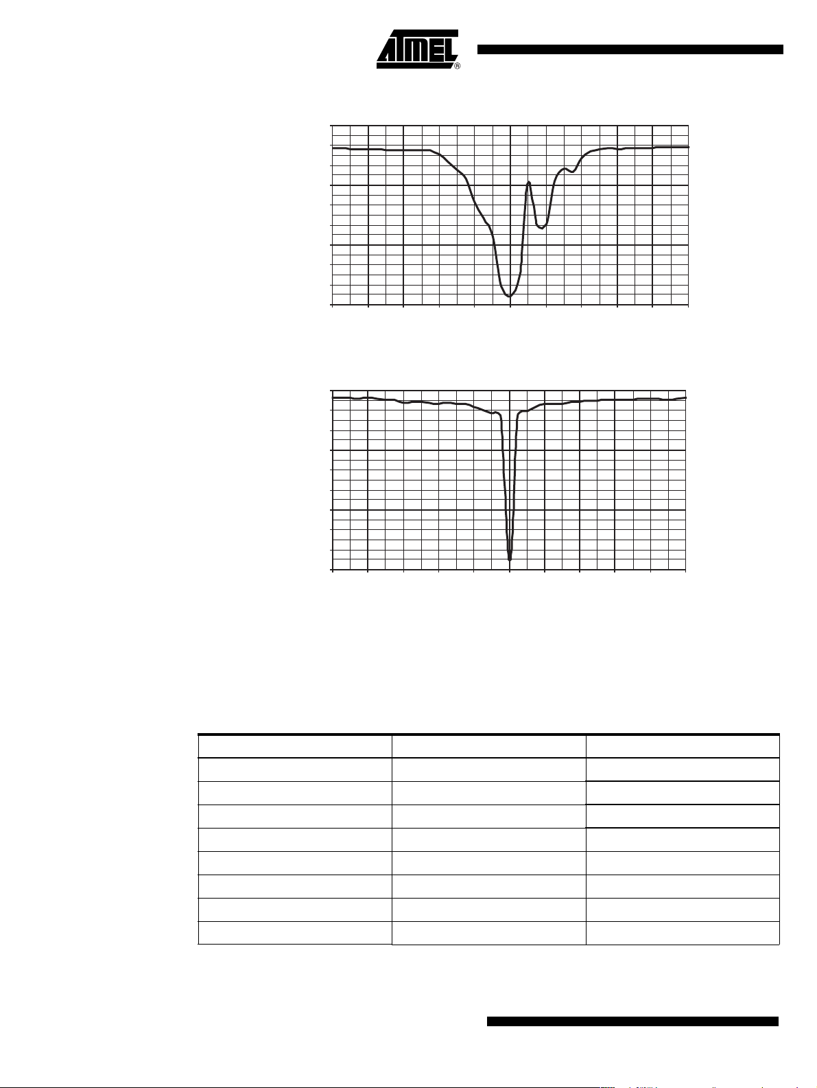
Figure 2-7. Narrow-band 3-dB Blocking Characteristic at 315 MHz
0
0
80.0
70 .0
60.0
50 .0
40.0
30.0
20.0
10 .0
Blocking Level (dBC)
0.0
-10.0
-5.0 -4 .0 -3 .0 - 2.0 -1.0 0.0 1.0 2.0 3.0 4.0 5.
Distance from Interfering to Receiving Signal (MHz)
Figure 2-8. Wide-band 3-dB Blocking Characteristic at 315 MHz
80.0
70 .0
60.0
50 .0
40.0
30.0
20.0
10 .0
Blocking Level (dBC)
0.0
-10.0
-50.0 -40.0 -30.0 -20.0 -10.0 0.0 10.0 20.0 30.0 40.0 50.
Distance from Interfering to Receiving Signal (MHz)
12
Table 2-8 shows the blocking performance measured relative to –102 dBm for some frequen-
cies. Note that sometimes the blocking is measured relative to the sensitivity level 104 dBm
(denoted dBS), instead of the carrier –102 dBm (denoted dBC)
Table 2-8. Blocking 3 dB Above Sensitivity Level With BER < 10
Frequency Offset Blocking Level Blocking
+1.5 MHz –44.5 dBm 57.5 dBC, 60.5 dBS
–1.5 MHz –44.5 dBm 57.5 dBC, 60.5 dBS
+2 MHz –39.0 dBm 63 dBC, 66 dBS
–2 MHz –36.0 dBm 66 dBC, 69 dBS
+3 MHz –34.5 dBm 67.5 dBC, 70.5 dBS
–3 MHz –34.5 dBm 67.5 dBC, 70.5 dBS
+20 MHz –28.0 dBm 74 dBC, 77 dBS
–20 MHz –28.0 dBm 74 dBC, 77 dBS
ATA5745/ATA5746 [Preliminary]
–3
4596A–RKE–05/06
Page 13
ATA5745/ATA5746 [Preliminary]
)
C
C
C
The ATA5745/ATA5746 can also receive FSK and ASK modulated signals if they are much
higher than the I1dBCP. It can typically receive useful signals at
to as the nonlinear dynamic range (that is, the maximum to minimum receiving signal), and is
95 dB for 10 Kbits/s Manchester (FSK). This value is useful if the transmitter and receiver are
very close to each other.
2.7 In-band Disturbers, Data Filter, Quasi-peak Detector, Data Slicer
If a disturbing signal falls into the received band, or if a blocker is not a continuous wave, the
performance of a receiver strongly depends on the circuits after the IF filter. Hence, the demodulator, data filter, and data slicer are important.
The data filter of the ATA5745/ATA5746 functions also as a quasi-peak detector. This results in a
good suppression of above mentioned disturbers and exhibits a good carrier-to-noise performance. The required useful-signal-to-disturbing-signal ratio, at a BER of 10
in ASK mode and less than 3 dB (BR_Range_0 to BR_Range_2) and 6 dB (BR_Range_3) in
FSK mode. Due to the many different possible waveforms, these numbers are measured for the
signal, as well as for disturbers, with peak amplitude values. Note that these values are
worst-case values and are valid for any type of modulation and modulating frequency of the disturbing signal, as well as for the receiving signal. For many combinations, lower
carrier-to-disturbing-signal ratios are needed.
–10 dBm. This is often referred
–3,
is less than 14 dB
2.8 RSSI Output
The output voltage of the pin RSSI is an analog voltage, proportional to the input power level.
Using the RSSI output signal, the signal strength of different transmitters can be distinguished.
The usable dynamic range of the RSSI amplifier is 65 dB, the input power range P(RF
IN
) is
–110 dBm to –45 dBm, and the gain is 15 mV/dB. Figure 2-9 shows the RSSI characteristic of a
typical device at 315 MHz with VS3V_AVCC = VS5V = 2.7V to 3.3V and T
= –40°C to
amb
+105°C with a matched input as shown in Table 2-2 and Figure 2-1 on page 6. At 433.92 MHz,
1 dB more signal level is needed for the same RSSI results.
Figure 2-9. Typical RSSI Characteristic at 315 MHz Versus Temperature and Supply Voltage
1.7
1.6
1.5
1.4
1.3
1.2
1.1
1.0
V_RSSI (V)
0.9
0.8
0.7
0.6
0.5
0.4
-130 -120 -110 -100 -90 -80 -70 -60 -50 -40 -30 -20 -10
Pin (dBm
min; -9dB
max; +9dB
2.7V, -40˚C
3.0V, -40˚C
3.3V, -40˚C
2.7V, 27˚C
3.0V, 27˚C
3.3V, 27˚C
2.7V, 105˚
3.0V, 105˚
3.3V, 105˚
4596A–RKE–05/06
13
Page 14

As can be seen in Figure 2-9 on page 13, for single devices there is a variance over temperature
and supply voltage range of ±3 dB. The total variance over production, temperature, and supply
voltage range is ±9 dB.
2.9 Frequency Synthesizer
The LO generates the carrier frequency for the mixer via a PLL synthesizer. The XTO (crystal
oscillator) generates the reference frequency f
erates the drive voltage frequency f
32 (ATA5745). The divided frequency is compared to f
current output of the phase frequency detector is connected to the fully integrated loop filter, and
thereby generates the control voltage for the VCO. By means of that configuration, the VCO is
controlled in a way, such that f
calculated using the following formula: f
phase noise of –130 dBC/Hz at 3 MHz and spurs of –75 dBC.
Care must be taken with the harmonics of the CLK output signal, as well as with the harmonics
produced by a microprocessor clocked using the signal, as these harmonics can disturb the
reception of signals.
3. XTO
The XTO is an amplitude-regulated Pierce oscillator type with external load capacitances
(2 × 16 pF). Due to additional internal and board parasitics (C
side, the load capacitance amounts to 2 × 18 pF (9 pF total).
. The VCO (voltage-controlled oscillator) gen-
XTO
for the mixer. fLO is divided by the factor 24 (ATA5746) or
LO
by the phase frequency detector. The
XTO
/24 (fLO/ 32) is equal to f
LO
XTO=fLO
/ 24 (f
. If fLO is determined, f
XTO
XTO=fLO
/ 32). The synthesizer has a
) of approximately 2 pF on each
P
XTO
can be
The XTO oscillation frequency f
is the reference frequency for the integer-N synthesizer.
XTO
When designing the system in terms of receiving and transmitting frequency offset, the accuracy
of the crystal and XTO have to be considered.
The XTO’s additional pulling (including the R
tolerance) is only ±5 ppm. The XTAL versus tem-
M
perature, aging, and tolerances is then the main source of frequency error in the local oscillator.
The XTO frequency depends on XTAL properties and the load capacitances C
and XTAL2. The pulling (p) of f
from the nominal f
XTO
is calculated using the following for-
XTAL
at pin XTAL1
L1,2
mula:
C
m
------- -
p
2
, the crystal's motional capacitance; C0, the shunt capacitance; and CLN, the nominal load
C
m
capacitance of the XTAL, are found in the datasheet. C
the crystal in the circuit, and consists of C
C
–
+()COCL+()×
OCLN
LNCL
---------------------------------------------------------------
C
10-6ppm××=
is the total actual load capacitance of
L
and CL2 connected in series.
L1
14
ATA5745/ATA5746 [Preliminary]
4596A–RKE–05/06
Page 15

ATA5745/ATA5746 [Preliminary]
Figure 3-1. Crystal Equivalent Circuit
XTAL
Crystal Equivalent Circuit
C
0
With C
C
L1
≤10 fF, C0≥ 1.0 pF, CLN= 9 pF and C
m
C
L2
L
m
CL = CL1 × CL2/ (CL1 + CL2)
= 16 pF ±1%, the pulling amounts to
L1,2
R
C
m
m
P ≤±1 ppm.
The C
of the XTAL has to be lower than C
0
/ 2 = 7.9 pF for a Pierce oscillator type in order to
Lmin
not enter the steep region of pulling versus load capacitance where there is risk of an unstable
oscillation.
To ensure proper start-up behavior, the small signal gain and the negative resistance provided
by this XTO at start is very large. For example, oscillation starts up even in the worst case with a
crystal series resistance of 1.5 kΩ at C
≤2.2 pF with this XTO. The negative resistance is
0
approximately given by
Z
⎧⎫
1Z3Z2Z3Z1Z3
Re Zxtocore{}Re
with Z
Z
Z
Z
and Z2 as complex impedances at pins XTAL1 and XTAL2, hence
1
=–j/(2× p × f
1
consists of crystal C0 in parallel with an internal 110-kΩ resistor, hence
3
=–j/(2× p × f
3
---------------------------------------------------------------------------------------- -
=
⎨⎬
Z
1Z2Z3Z1Z2
⎩⎭
× CL1)+5Ω and Z2=–j/(2× p × f
XTO
× C0)/110kΩ, gm is the internal transconductance between XTAL1 and
XTO
gm××+×+×
gm××+++
× CL2)+5Ω.
XTO
XTAL2, with typically 20 mS at 25°C.
4596A–RKE–05/06
With f
= 13.5 MHz, gm = 20 mS, CL= 9 pF, and C0= 2.2 pF, this results in a negative resis-
XTO
tance of about 2 kΩ. The worst case for technology, supply voltage, and temperature variations
is then always higher than 1.4 kΩ for C
≤2.2 pF.
0
Due to the large gain at start, the XTO is able to meet a very low start-up time. The oscillation
start-up time can be estimated with the time constant τ.
τ
------------------------------------------------------------------------------------------------------------------ -=
4 π2f
XTAL
2
2
C
Re Z
m
()Rm+()××××
xtocore
After 10τ to 20τ, an amplitude detector detects the oscillation amplitude and sets XTO_OK to
High if the amplitude is large enough; this activates the CLK_OUT output if it is enabled via the
pins CLK_OUT_CTRL0 and CLK_OUT_CTRL1. Note that the necessary conditions of the
DVCC voltage also have to be fulfilled.
It is recommended to use a crystal with C
C
= 1.0 pF to 2.2 pF.
0
= 3.0 fF to 10 fF, CLN=9pF, Rm<120Ω and
m
15
Page 16

Lower values of Cm can be used, slightly increasing the start-up time. Lower values of C0 or
higher values of C
(up to 15 fF) can also be used, with only little influence on pulling.
m
Figure 3-2. XTO Block Diagram
C
L1
XTAL1 XTAL2 CLK_OUT
The relationship between f
C
L2
CLK_OUT_CTRL1CLK_OUT_CTRL0
f
FXTO
and the fRF is shown in Table 3-1.
XTO
Divider
/3, /6, /12
Amplitude
Detector
Divider
/16
f
DCLK
&
XTO_OK
Table 3-1. Calculation of f
Frequency [MHz] f
433.92 (ATA5745) 13.57375 f
315.0 (ATA5746) 13.1433 f
Attention must be paid to the harmonics of the CLK_OUT output signal f
RF
[MHz] f
XTO
XTO
XTO
RF
x 32 – 440 kHz
x 24 – 440 kHz
CLK_OUT
as well as to the
harmonics produced by an microprocessor clocked with it, since these harmonics can disturb
the reception of signals if they get to the RF input. If the CLK_OUT signal is used, it must be
carefully laid out on the application PCB. The supply voltage of the microcontroller must also be
carefully blocked.
16
ATA5745/ATA5746 [Preliminary]
4596A–RKE–05/06
Page 17

3.1 Pin CLK_OUT
ATA5745/ATA5746 [Preliminary]
Pin CLK_OUT is an output to clock a connected microcontroller. The clock is available in
Standby and Active modes. The frequency f
CLK_OUT
CLK_OUT_CTRL0 and CLK_OUT_CTRL1, and is calculated as follows:
can be adjusted via the pins
Table 3-2. Setting of f
CLK_OUT_CTRL1 CLK_OUT_CTRL0 Function
00
01 f
10 f
11 f
CLK_OUT
The signal at CLK_OUT output has a nominal 50% duty cycle. To save current, it is recommended that CLK_OUT be switched off during Standby mode.
3.2 Basic Clock Cycle of the Digital Circuitry
The complete timing of the digital circuitry is derived from one clock. As seen in Figure 3-2 on
page 16, this clock cycle, T
divider.
f
XTO
f
DCLK
T
DCLK
-----------=
16
controls the following application relevant parameters:
- Debouncing of the data signal stream
, is derived from the crystal oscillator (XTO) in combination with a
DCLK
Clock on pin CLK_OUT is switched off
(Low level on pin CLK_OUT)
CLK_OUT=fXTO
CLK_OUT=fXTO
CLK_OUT=fXTO
/3
/6
/12
- Start-up time of the RX signal path
The start-up time and the debounce characteristic depend on the selected bit rate range
(BR_Range) which is defined by pins BR0 and BR1. The clock cycle T
is defined by the fol-
XDCLK
lowing formulas for further reference:
BR_Range ⇒ BR_Range 0: T
BR_Range 1: T
BR_Range 2: T
BR_Range 3: T
XDCLK
XDCLK
XDCLK
XDCLK
= 8 × T
= 4 × T
= 2 × T
= 1 × T
DCLK
DCLK
DCLK
DCLK
4596A–RKE–05/06
17
Page 18

4. Sensitivity Reduction
The output voltage of the RSSI amplifier is internally compared to a threshold voltage V
V
is determined by the value of the external resistor R
Th_red
the pins SENSE and VS3V_AVCC (see Figure 10-1 on page 28). The output of the comparator
is fed into the digital control logic. By this means, it is possible to operate the receiver at a lower
sensitivity.
If the level on input pin SENSE_CTRL is low, the receiver operates at full sensitivity.
If the level on input pin SENSE_CTRL is high, the receiver operates at a lower sensitivity. The
reduced sensitivity is defined by the value of R
nal-to-noise ratio of the LNA input. The reduced sensitivity depends on the signal strength at the
output of the RSSI amplifier.
Since different RF input networks may exhibit slightly different values for the LNA gain, the sensitivity values given in the electrical characteristics refer to a specific input matching. This
matching is illustrated in Figure 2-1 on page 6 and exhibits the best possible sensitivity.
If the sensitivity reduction feature is not used, pin SENSE can be left open, pin SENSE_CTRL
must be set to GND.
To operate with reduced sensitivity, pin SENSE_CTRL must be set to high before the RX signal
path will be enabled by setting pin RX to high (see Figure 4-1 on page 19). As long as the RSSI
level is lower than V
pin DATA_OUT (low level on pin DATA_OUT). An internal RS flip-flop will be set to high the first
time the RSSI voltage crosses V
DATA_OUT. From then on the receiver also works with full sensitivity. This makes sure that a
telegram will not be interrupted if the RSSI level varies during the transmission. The RS flip-flop
can be set back, and thus the receiver switched back to reduced sensitivity, by generating a positive pulse on pin ASK_NFSK (see Figure 4-2 on page 19). In FSK mode, operating with reduced
sensitivity follows the same way.
(defined by the external resistor R
Th_red
, and from then on the data stream will be available on pin
Th_red
. R
Sense
, the maximum sensitivity by the sig-
Sense
) no data stream is available on
Sense
is connected between
Sense
Th_red
.
18
ATA5745/ATA5746 [Preliminary]
4596A–RKE–05/06
Page 19

ATA5745/ATA5746 [Preliminary]
Figure 4-1. Reduced Sensitivity Active
ENABLE
ASK_NFSK
SENSE_CTRL
RX
V
Th_red
RSSI
DATA_OUT
t
Startup_PLL
t
Startup_Sig_Proc
Figure 4-2. Restart Reduced Sensitivity
ENABLE
ASK_NFSK
SENSE_CTRL
RX
V
Th_red
RSSI
t
Startup_Sig_Proc
4596A–RKE–05/06
DATA_OUT
19
Page 20

5. Power Supply
Figure 5-1. Power Supply
VS3V_AVCC
IN
V_REG
3.0V typ.
OUT
SW_DVCC
DVC CVS5V
5.1 OFF Mode
RX
EN
The supply voltage range of the ATA5745/ATA5746 is 2.7V to 3.3V or 4.5V to 5.5V.
Pin VS3V_AVCC is the supply voltage input for the range 2.7V to 3.3V, and is used in battery
applications using a single lithium 3V cell. Pin VS5V is the voltage input for the range 4.5V to
5.5V (car applications) in this case the voltage regulator V_REG regulates VS3V_AVCC to typically 3.0V. If the voltage regulator is active, a blocking capacitor of 2.2 µF has to be connected to
VS3V_AVCC (see Figure 10-1 on page 28).
DVCC is the internal operating voltage of the digital control logic and is fed via the switch
SW_DVCC by VS3V_AVCC. DVCC must be blocked on pin DVCC with 68 nF (see Figure 9-1
on page 27 and Figure 10-1 on page 28).
Pin RX is the input to activate the RX signal processing and set the receiver to Active mode.
A low level on pin RX and ENABLE will set the receiver to OFF mode (low power mode). In this
mode, the crystal oscillator is shut down and no clock is available on pin CLK_OUT. The
receiver is not sensitive to a transmitter signal in this mode.
Table 5-1. Standby Mode
RX ENABLE Function
00 OFF mode
5.2 Standby Mode
20
ATA5745/ATA5746 [Preliminary]
The receiver activates the Standby mode if pin ENABLE is set to “1”.
In Standby mode, the XTO is running and the clock on pin CLK_OUT is available after the
start-up time of the XTO has elapsed (dependent on pin CLK_OUT_CTRL0 and
CLK_OUT_CTRL1). During Standby mode, the receiver is not sensitive to a transmitter signal.
In Standby mode, the RX signal path is disabled and the power consumption I
Standby
is typically
50 µA (CLK_OUT output off, VS3V_AVCC = VS5V = 3V). The exact value of this current is
strongly dependent on the application and the exact operation mode, therefore check the section “Electrical Characteristics: General” on page 29 for the appropriate application case.
Table 5-2. Standby Mode
RX ENABLE Function
0 1 Standby mode
4596A–RKE–05/06
Page 21

ATA5745/ATA5746 [Preliminary]
Figure 5-2. Standby Mode (CLK_OUT_CTRL0 or CLK_OUT_CTRL1 = 1)
CLK_OUT
t
XTO_Startup
ENABLE
5.3 Active Mode
The Active mode is enabled by setting the level on pin RX to high. In Active mode, the RX signal
path is enabled and if a valid signal is present it will be transferred to the connected
microcontroller.
Table 5-3. Active Mode
RX ENABLE Function
1 1 Active mode
Standby Mode
Figure 5-3. Active Mode
CLK_OUT
ENABLE
RX
DATA_OUT
During T
Startup_PLL
circuit starts up (T
the PLL is enabled and starts up. If the PLL is locked, the signal processing
Startup_Sig_Proc
). After the start-up time, all circuits are in stable condition and
ready to receive. The duration of the start-up sequence depends on the selected bit rate range.
DATA_OUT valid
t
Startup_PLL
I
Standby
Standby Mode Active Mode
I
Startup_PLL
Startup
t
Startup_Sig_Proc
I
Active
I
Active
4596A–RKE–05/06
21
Page 22

Table 5-4. Start-up Time
ATA5745 (433.92 MHz) ATA5746 (315 MHz)
BR1 BR0
00
0 1 644 µs 665 µs
1 0 417 µs 431 µs
T
Startup_PLL
261 µs
T
Startup_Sig_Proc
1096 µs
T
Startup_PLL
269 µs
T
1 1 304 µs 324 µs
Table 5-5. Modulation Scheme
ASK_NFSK RF
0
1
at Pin LNA_IN Level at Pin DATA_OUT
IN
f
FSK_H
f
FSK_L
on 1
f
ASK
off 0
f
ASK
1
0
Startup_Sig_Proc
1132 µs
22
ATA5745/ATA5746 [Preliminary]
4596A–RKE–05/06
Page 23

ATA5745/ATA5746 [Preliminary]
6. Bit Rate Ranges
Configuration of the bit rate ranges is carried out via the two pins BR0 and BR1. The microcontroller uses these two interface lines to set the corner frequencies of the band-pass data filter.
Switching the bit rate ranges while the RF front end is in Active mode can be done on the fly and
will not take longer than 100 µs if done while remaining in either ASK or FSK mode. If the modulation scheme is changed at the same time, the switching time is (T
on page 25). Each BR_Range is defined by a minimum edge-to-edge time. To maintain full sen-
sitivity of the receiver, edge-to-edge transition times of incoming data should not be less than the
minimum for the selected BR_Range.
Table 6-1. BR Ranges ASK
Minimum Edge-to-edge
Time Period T
Signal
of the Data
EE
(2)
BR1 BR0 BR_Range
Recommended Bit Rate
(Manchester)
(1)
0 0 BR_Range0 1.0 Kbit/s to 2.5 Kbits/s 200 µs 200 µs to 500 µs
0 1 BR_Range1 2.0 Kbits/s to 5.0 Kbits/s 100 µs 100 µs to 250 µs
1 0 BR_Range2 4.0 Kbits/s to 10.0 Kbits/s 50 µs 50 µs to 125 µs
1 1 BR_Range3 8.0 Kbits/s to 10.0 Kbits/s 50 µs 50 µs to 62.5 µs
Startup_Sig_Proc
Edge-to-edge Time Period TEE of
the Data Signal During the Start-up
Period
, see Figure 7-1
(3)
Table 6-2. BR Ranges FSK
Minimum Edge-to-edge
BR1 BR0 BR_Range
Recommended Bit Rate
(Manchester)
(1)
Time Period T
EE
Signal
of the Data
(2)
0 0 BR_Range0 1.0 Kbit/s to 2.5 Kbits/s 200 µs 200 µs to 500 µs
0 1 BR_Range1 2.0 Kbits/s to 5.0 Kbits/s 100 µs 100 µs to 250 µs
1 0 BR_Range2 4.0 Kbits/s to 10.0 Kbits/s 50 µs 50 µs to 125 µs
1 1 BR_Range3 8.0 Kbits/s to 20.0 Kbits/s 25 µs 25 µs to 62.5 µs
Note: If during the start-up period (T
Startup_PLL+TStartup_Sig_Proc
) there is no RF signal, the data filter settles to the noise floor, leading
to noise on pin DATA_OUT.
Notes: 1. As can be seen, a bit stream of, for example, 2.5 Kbits/s can be received in BR_Range0 and BR_Range1 (overlapping
BR_Ranges). To get the full sensitivity, always use the lowest possible BR_Range (here, BR_Range0). The advantage in
the next higher BR_Range (BR_Range1) is the shorter start-up period, meaning lower current consumption during Polling
mode. Thus, it is a decision between sensitivity and current consumption.
2. The receiver is also capable of receiving non-Manchester-modulated signals, such as PWM, PPM, VPWM, NRZ. In ASK
mode, the header and blanking periods occurring in Keeloq-like protocols (up to 52 ms) are supported.
3. To ensure an accurate settling of the data filter during the start-up period (T
time T
of the data signal (preamble) must be inside the given limits during this period.
EE
Startup_PLL
Edge-to-edge Time Period TEE of
the Data Signal During the Start-up
+ T
Startup_Sig_Proc
(3)
Period
), the edge-to-edge
4596A–RKE–05/06
23
Page 24

Figure 6-1. Examples of Supported Modulation Formats
T
T
EE
T
T
EE
VPWM: On Transition Low to High
On Transition High to Low
EE
EETEE
TEET
EE
Logic 1MAN: Logic 0
TEETEET
EE
Logic 1PWM: Logic 0
Logic 1Logic 0
T
T
EE
EE
T
EE
Logic 1Logic 0
T
T
EE
T
EE
EE
T
T
EE
EETEE
T
EE
Figure 6-2. Supported Header and Blanking Periods
Preamble Header Data BurstGuard TimeData Burst
TEETEET
EE
Logic 1PPM: Logic 0
T
EE
Logic 1NRZ: Logic 0
24
ATA5745/ATA5746 [Preliminary]
4596A–RKE–05/06
Page 25

ATA5745/ATA5746 [Preliminary]
7. ASK_NFSK
The ASK_NFSK pin allows the microcontroller to rapidly switch the RF front end between
demodulation modes. A logic 1 on this pin selects ASK mode, and a logic 0 FSK mode. The time
to change modes (T
Startup_Sig_Proc
rate range) and is given in Table 5-4 on page 22. This response time is specified for applications
that require an ASK preamble followed by FSK data (for typical TPM applications). During
T
Startup_Sig_Proc
, the level on pin DATA_OUT is low.
Figure 7-1. ASK Preamble 2.4 Kbits/s followed by FSK Data 9.6 Kbits/s
ENABLE
RX
BR1
) depends on the bit rate range being selected (not current bit
BR0
ASK_NFSK
DATA_OUT Data valid BR3Data valid BR0
T
Startup_Sig_Proc
4596A–RKE–05/06
25
Page 26

8. Polling Current Calculation
Figure 8-1. Polling Cycle
ENABLE
RX
I
Active
Startup_PLL
I
I
Supply
I
Standby
T
(= 1 / Signal_Bitrate (average)
Bitcheck
T
Startup_Sig_Proc
T
Startup_PLL
(Startup Signal Processing)
(Startup RF-PLL)
I
Standby
In an RKE and TPM system, the average chip current in Polling mode, I
Polling
I
Active
Startup_PLL
I
, is an important
parameter. The polling period must be controlled by the connected microcontroller via the pins
ENABLE and RX. The polling current can be calculated as follows:
I
=(T
Polling
(T
Bitcheck/TPolling_Period
T
Polling_Period
T
Startup_PLL
T
Startup_Sig_Proc
Startup_PLL/TPolling_Period
× I
Standby
: depends on 315 MHz/433.92 MHz application.
: depends on 315 MHz/433.92 MHz application and the selected bit
) × I
Active
) × I
Startup_PLL
+(T
Polling_Period–TStartup_PLL–TStartup_Sig_Proc–TBitcheck
+(T
Startup_Sig_Proc/TPolling_Period
) × I
Active
)/
rate range.
T
T
I
I
: depends on the signal bit rate (1 / Signal_Bit_Rate).
Bitcheck
Polling_Period
Startup_PLL
Active
: depends on the transmitter telegram (preburst).
: depends on 3V or 5V application and the setting of pin CLK_OUT.
: depends on 3V or 5V application, ASK or FSK mode and the setting of
pin CLK_OUT.
I
: depends on 3V or 5V application and the setting of pin CLK_OUT.
Standby
Example:- 315-MHz application (ATA5746), bit rate: 9.6 Kbits/s, T
--> T
Startup_PLL
--> T
Startup_Sig_Proc
--> T
Bitcheck
= 269 µs
= 324 µs (Bit Rate Range 3)
= 104 µs
Polling_Period
=8ms
3V application; ASK mode, CLK_OUT disabled
--> I
--> I
--> I
--> I
Startup_PLL
Active
Standby
Polling
=4.5mA
=6.5mA
=0.05mA
= 0.545 mA
+
26
ATA5745/ATA5746 [Preliminary]
4596A–RKE–05/06
Page 27

9. 3V Application
z
Figure 9-1. 3V Application
ATA5745/ATA5746 [Preliminary]
15 nF
Microcontroller
output
output
output
output
input
output
VCCVSS
TEST2
DATA_OUT
TEST1
CLK_OUT
CLK_OUT_CTRL1
CLK_OUT_CTRL0
ENABLE
XTAL2
18 pF
CDEM
ASK_NFSK
ATA5745/
ATA5746
DVC C
XTAL1
68 nF
18 pF
VCC = 2.7V to 3.3V
BR1
VS5V
RX
BR0
TEST3
RSSI
SENSE_CTRL
SENSE
LNA_IN
LNA_GND
GND
VS3V_AVCC
68 nF
2.2 pF
68 nH/36 nH
315 MHz/433.92 MH
RF
IN
4596A–RKE–05/06
Note: Paddle (backplane) must be connected to GND
27
Page 28

10. 5V Application
Figure 10-1. 5V Application With Reduced/Full Sensitivity
15 nF
Microcontroller
output
output
output
output
output
input
output
VCCVSS
TEST2
DATA_OUT
TEST1
CLK_OUT
CLK_OUT_CTRL1
CLK_OUT_CTRL0
ENABLE
XTAL2
18 pF
68 nF
CDEM
BR1
ASK_NFSK
ATA5745/
ATA5746
VS5V
DVC C
XTAL1
68 nF
18 pF
VCC = 4.5V to 5.5V
RX
BR0
TEST3
RSSI
SENSE_CTRL
SENSE
LNA_IN
LNA_GND
GND
VS3V_AVCC
315 MHz/433.92 MHz
2.2 µF
R
Sense
68 nH/36 nH
2.2 pF
RF
IN
28
Note: Paddle (backplane) must be connected to GND
ATA5745/ATA5746 [Preliminary]
4596A–RKE–05/06
Page 29

ATA5745/ATA5746 [Preliminary]
11. Absolute Maximum Ratings
Stresses beyond those listed under “Absolute Maximum Ratings” may cause permanent damage to the device. This is a stress rating
only and functional operation of the device at these or any other conditions beyond those indicated in the operational sections of this
specification is not implied. Exposure to absolute maximum rating conditions for extended periods may affect device reliability.
Parameters Symbol Min. Max. Unit
Junction temperature T
Storage temperature T
Ambient temperature T
Supply voltage VS5V V
ESD (Human Body Model ESD S 5.1)
every pin
ESD (Machine Model JEDEC A115A)
every pin
ESD (Field Induced Charge Device Model ESD
STM 5.3.1-1999) every pin
Maximum input level, input matched to 50Ω P
j
stg
amb
S
–55 +125 °C
–40 +105 °C
HBM –4 +4 kV
MM –200 +200 V
FCDM –500 +500 V
in_max
12. Thermal Resistance
Parameters Symbol Value Unit
Junction ambient R
thJA
25 K/W
+150 °C
+6 V
0dBm
13. Electrical Characteristics: General
All parameters refer to GND and are valid for T
Typical values are given at V
VS3V_AVCC=VVS5V
consumption, timing, and digital pin properties can be found in the specific sections of the “Electrical Characteristics”.
No. Parameters Test Conditions Pin
1 OFF Mode
V
Supply current in OFF
1.1
mode
VS3V_AVCC=VVS5V
=5V
V
VS5V
CLK_OUT disabled
2 Standby Mode
RF operating frequency
2.1
range
ATA5746 14 f
ATA5745 14 f
XTO running
V
VS3V_AVCC=VVS5V
Supply current
2.2
Standby mode
CLK_OUT disabled
XTO running
V
=5V
VS5V
CLK_OUT disabled
XTO startup
2.3 System start-up time
XTAL: C
m
C0= 1.8 pF, Rm= 15Ω
*) Type means: A = 100% tested, B = 100% correlation tested, C = Characterized on samples, D = Design parameter
Note: 1. Pin numbers in parenthesis were measured with RF_IN matched to 50Ω according to Figure 2-1 on page 6 with component
values as in Table 2-2 on page 6 (RF
= –40°C to +105°C, V
amb
=3V, T
= 25°C, and fRF= 315 MHz unless otherwise specified. Details about current
amb
≤ 3V
≤ 3V
= 5 fF,
).
IN
VS3V_AVCC=VVS5V
(1)
10, 11
10 I
10,11 I
10,11 I
T
= 2.7V to 3.3V, and V
= 4.5V to 5.5V.
VS5V
Symbol Min. Typ. Max. Unit Type*
SOFF
RF
RF
Standby
Standby
XTO_Startup
2
2
313 317 MHz A
433 435 MHz A
50 100 µA A
50 100 µA A
0.3 0.8 ms A
µA
µA
A
A
4596A–RKE–05/06
29
Page 30

13. Electrical Characteristics: General (Continued)
All parameters refer to GND and are valid for T
Typical values are given at V
VS3V_AVCC=VVS5V
consumption, timing, and digital pin properties can be found in the specific sections of the “Electrical Characteristics”.
No. Parameters Test Conditions Pin
From Standby mode to
Active mode
2.4 Active mode start-up time
BR_Range_3
ATA5745
ATA5746
3 Active Mode
V
VS3V_AVCC=VVS5V
ASK mode
CLK_OUT disabled
SENSE_CTRL = 0
V
VS3V_AVCC=VVS5V
FSK mode
CLK_OUT disabled
Supply current Active
3.1
mode
SENSE_CTRL = 0
V
=5V
VS5V
ASK mode
CLK_OUT disabled
SENSE_CTRL = 0
V
=5V
VS5V
FSK mode
CLK_OUT disabled
SENSE_CTRL = 0
V
VS3V_AVCC=VVS5V
T
Supply current Polling
3.2
mode
Poll ing_Pe riod
BR_Range_3, ASK mode,
CLK_OUT disabled
Data rate = 9.6 Kbits/s
FSK deviation
f
= ±38 kHz
DEV
BER = 10
T
= 25°C
amb
Input sensitivity FSK
3.3
= 315 MHz
f
RF
Bit rate 9.6 Kbits/s BR2 (14) P
Bit rate 2.4 Kbits/s BR0 (14) P
FSK deviation ±18 kHz to
±50 kHz
Bit rate 9.6 Kbits/s BR2 (14) P
Bit rate 2.4 Kbits/s BR0 (14) P
ASK 100% level of carrier,
BER = 10
Input sensitivity ASK
3.4
= 315 MHz
f
RF
T
= 25°C
amb
Bit rate 9.6 Kbits/s BR2 (14) P
Bit rate 2.4 Kbits/s BR0 (14) P
*) Type means: A = 100% tested, B = 100% correlation tested, C = Characterized on samples, D = Design parameter
Note: 1. Pin numbers in parenthesis were measured with RF_IN matched to 50Ω according to Figure 2-1 on page 6 with component
values as in Table 2-2 on page 6 (RF
= –40°C to +105°C, V
amb
=3V, T
= 25°C, and fRF= 315 MHz unless otherwise specified. Details about current
amb
=3V
=3V
=3V
= 8 ms
–
3
–
3
).
IN
VS3V_AVCC=VVS5V
(1)
Symbol Min. Typ. Max. Unit Type*
T
Startup_PLL
T
Startup_Sig_Proc
10,11 I
10,11 I
10 I
10 I
10,11 I
Active
Active
Active
Active
Polling
REF_FSK
REF_FSK
REF_FSK
REF_FSK
REF_ASK
REF_ASK
= 2.7V to 3.3V, and V
= 4.5V to 5.5V.
VS5V
+
565
593
6.5 mA A
6.7 mA A
6.7 mA A
6.9 mA A
545 µA C
–103 –105 –106.5 dBm B
–106 –108 –109.5 dBm B
–101 dBm B
–104 dBm B
–109 –111 –112.5 dBm B
–112 –114 –115.5 dBm B
A
µs
µs
30
ATA5745/ATA5746 [Preliminary]
4596A–RKE–05/06
Page 31

ATA5745/ATA5746 [Preliminary]
13. Electrical Characteristics: General (Continued)
All parameters refer to GND and are valid for T
Typical values are given at V
VS3V_AVCC=VVS5V
consumption, timing, and digital pin properties can be found in the specific sections of the “Electrical Characteristics”.
No. Parameters Test Conditions Pin
f
Sensitivity change at
=433.92MHz
f
RF
3.5
compared to
fRF=315MHz
Sensitivity change versus
temperature, supply
3.6
voltage and frequency
offset
= 315 MHz to
RF
=433.92MHz
f
RF
P=P
REF_ASK
P=P
REF_FSK
FSK f
DEV
∆f
OFFSET
ASK 100%
∆f
OFFSET
P = P
REF_ASK
∆P
REF2
P = P
REF_FSK
∆P
REF2
connected from
R
Sense
pin SENSE to
pin VS3V_AVCC
= 62 kΩ
R
Sense
fin = 433.92 MHz
R
Reduced sensitivity
3.7
= 82 kΩ
Sense
= 433.92 MHz
f
in
= 62 kΩ
R
Sense
fin = 315 MHz
= 82 kΩ
R
Sense
= 315 MHz
f
in
Reduced sensitivity
variation over full
operating range
R
R
P
Sense
Sense
Red
= 62 kΩ
= 82 kΩ
= P
Maximum frequency
difference of f
receiver and transmitter in
Maximum frequency
3.8
offset in FSK mode
FSK mode (f
center frequency of the
FSK signal with
= 10 Kbits/s
f
BIT
= ±38 kHz
f
DEV
With up to 2 dB
loss of sensitivity.
Note that the tolerable
Supported FSK
3.9
frequency deviation
frequency offset is 12 kHz
lower for f
than for f
hence,
≤ ±148 kHz
OFFSET
= 315 MHz (14) NF 6.0 9 dB B
= 433.92 MHz (14) NF 7.0 10 dB B
3.10 System noise figure
∆f
f
f
RF
RF
*) Type means: A = 100% tested, B = 100% correlation tested, C = Characterized on samples, D = Design parameter
Note: 1. Pin numbers in parenthesis were measured with RF_IN matched to 50Ω according to Figure 2-1 on page 6 with component
values as in Table 2-2 on page 6 (RF
= –40°C to +105°C, V
amb
=3V, T
amb
+ ∆P
REF1
+ ∆P
REF1
= ±38 kHz
≤ ±160 kHz
≤ ±160 kHz
+ ∆P
REF1
+ ∆P
REF1
+ P
Ref_Red
DEV
DEV
∆Red
between
RF
is the
RF
= ±50 kHz
= ±38 kHz,
).
IN
VS3V_AVCC=VVS5V
= 2.7V to 3.3V, and V
= 4.5V to 5.5V.
VS5V
= 25°C, and fRF= 315 MHz unless otherwise specified. Details about current
(1)
Symbol Min. Typ. Max. Unit Type*
+
(14) ∆P
(14) ∆P
REF1
REF2
+4.5 –1.5 B
+1 dB B
+
dBm
P
Ref_Red
(peak
level)
–76 dBm C
–88 dBm C
–76 dBm C
–88 dBm C
(14) ∆f
(14) f
∆P
Red
OFFSET
DEV
–10 +10 dB
–160 +160 kHz B
±18 ±38 ±50 kHz B
4596A–RKE–05/06
31
Page 32

13. Electrical Characteristics: General (Continued)
All parameters refer to GND and are valid for T
Typical values are given at V
VS3V_AVCC=VVS5V
consumption, timing, and digital pin properties can be found in the specific sections of the “Electrical Characteristics”.
No. Parameters Test Conditions Pin
= 433.92 MHz f
f
3.11 Intermediate frequency
RF
= 315 MHz f
f
RF
3 dB bandwidth
This value is for
information only!
3.12 System bandwidth
Note that for crystal and
system frequency offset
calculations, ∆f
must be used.
∆f
= 1.8 MHz
System out-band
3.13
3rd-order input intercept
point
System outband input
3.14
1-dB compression point
3.15 LNA input impedance
Maximum peak RF input
3.16
level, ASK and FSK
meas1
= 3.6 MHz
∆f
meas2
f
= 315 MHz
RF
= 433.92 MHz (14) IIP3 –23 dBm C
f
RF
= 1 MHz
∆f
meas1
f
= 315 MHz
RF
f
= 433.92 MHz (14) I1dBCP –30 –35 dBm C
RF
= 315 MHz 14 Z
f
RF
= 433.92 MHz 14 Z
f
RF
BER < 10
FSK: f
DEV
f < 1 GHz (14) –57 dBm C
f >1 GHz (14) –47 dBm C
= 315.44 MHz
f
LO
2 × f
3.17 LO spurs at LNA_IN
LO
4 × f
LO
= 434.36 MHz
f
LO
2 × f
LO
4 × f
LO
With the complete image
3.18 Image rejection
band
= 315 MHz (14) 24 30 dB
f
RF
f
= 433.92 MHz (14) 24 30 dB A
RF
Peak level of useful signal
to peak level of interferer
for BER < 10
Useful signal to interferer
3.19
ratio
modulation scheme of
interferer
FSK BR_Ranges 0, 1, 2 (14) SNR
FSK BR_Range_3 (14) SNR
ASK (P
RF
*) Type means: A = 100% tested, B = 100% correlation tested, C = Characterized on samples, D = Design parameter
Note: 1. Pin numbers in parenthesis were measured with RF_IN matched to 50Ω according to Figure 2-1 on page 6 with component
values as in Table 2-2 on page 6 (RF
= –40°C to +105°C, V
amb
=3V, T
= 25°C, and fRF= 315 MHz unless otherwise specified. Details about current
amb
VS3V_AVCC=VVS5V
(1)
(14) SBW 435 kHz A
OFFSET
(14) IIP3 –24 dBm C
(14) I1dBCP –31 –36 dBm C
–
3
, ASK: 100% (14) P
= ±38 kHz (14) P
(14)
(14)
–
3
with any
< P
RFIN_High
)(14)SNR
).
IN
= 2.7V to 3.3V, and V
= 4.5V to 5.5V.
VS5V
Symbol Min. Typ. Max. Unit Type*
IF
IF
in_LNA
in_LNA
IN_max
IN_max
440 kHz A
440 kHz A
(72.4 – j298) Ω C
(55 – j216) Ω C
+5 –10 dBm C
+5 –10 dBm C
–90
–94
dBm C
–68
–92
–88
dBm C
–58
A
FSK0-2
FSK3
ASK
23dBB
46dBB
10 14 dB B
32
ATA5745/ATA5746 [Preliminary]
4596A–RKE–05/06
Page 33

ATA5745/ATA5746 [Preliminary]
13. Electrical Characteristics: General (Continued)
All parameters refer to GND and are valid for T
Typical values are given at V
VS3V_AVCC=VVS5V
consumption, timing, and digital pin properties can be found in the specific sections of the “Electrical Characteristics”.
No. Parameters Test Conditions Pin
Dynamic range (14),17 D
Lower level of range
= 315 MHz
f
RF
f
= 433.92 MHz
RF
3.20 RSSI output
Upper level of range
= 315 MHz
f
RF
= 433.92 MHz
f
RF
Gain (14),17 15 mV/dB A
Output voltage range (14),17 V
Output resistance
3.21
RSSI pin
Sensitivity (BER = 10
reduced by 3 dB if a
continuous wave blocking
signal at ±∆f is ∆P
higher than the useful
signal level
(Bit rate = 10 Kbits/s,
FSK, f
DEV
Manchester code,
BR_Range2)
= 315 MHz
f
3.22 Blocking
RF
∆f ± 1.5 MHz
∆f ± 2 MHz
∆f ± 3 MHz
∆f ± 10 MHz
∆f ± 20 MHz
= 433.92 MHz
f
RF
∆f ± 1.5 MHz
∆f ± 2 MHz
∆f ± 3 MHz
∆f ± 10 MHz
∆f ± 20 MHz
3.23 CDEM
Capacitor connected to
pin 23 (CDEM)
*) Type means: A = 100% tested, B = 100% correlation tested, C = Characterized on samples, D = Design parameter
Note: 1. Pin numbers in parenthesis were measured with RF_IN matched to 50Ω according to Figure 2-1 on page 6 with component
values as in Table 2-2 on page 6 (RF
= –40°C to +105°C, V
amb
=3V, T
= 25°C, and fRF= 315 MHz unless otherwise specified. Details about current
amb
–
3
) is
Block
±38kHz,
).
IN
VS3V_AVCC=VVS5V
(1)
(14),17 P
(14),17 P
17 R
= 2.7V to 3.3V, and V
Symbol Min. Typ. Max. Unit Type*
RSSI
RFIN_Low
RFIN_High
RSSI
RSSI
350 1600 mV A
81012.5kΩ C
65 dB A
–110 dBm A
–45 dBm A
= 4.5V to 5.5V.
VS5V
57.5
(14) ∆P
Block
63.0
67.5
dBC C
72.0
74.0
56.5
(14) ∆P
Block
62.0
66.5
dBC C
71.0
73.0
23 –5% 15 +5% nF D
4596A–RKE–05/06
33
Page 34

13. Electrical Characteristics: General (Continued)
All parameters refer to GND and are valid for T
Typical values are given at V
VS3V_AVCC=VVS5V
consumption, timing, and digital pin properties can be found in the specific sections of the “Electrical Characteristics”.
No. Parameters Test Conditions Pin
4XTO
Transconductance XTO at
4.1
start
4.2 XTO start-up time
4.3 Maximum C
of XTAL 7,8 C
0
Pulling of LO frequency
due to XTO, CL1 and
f
LO
4.4
CL2 versus temperature
and supply changes
At startup; after startup
the amplitude is regulated
to V
PPXTAL
≤ 2.2 pF
C
0
Cm < 14 fF
≤ 120Ω
R
m
1.0 pF ≤ C
= 4.0 fF to 7.0 fF
C
m
Rm ≤ 120Ω
Cm=5fF, C0=1.8pF
Rm= 15Ω
Amplitude XTAL after
4.5
startup
V(XTAL1, XTAL2)
peak-to-peak value
V(XTAL1)
peak-to-peak value
≤ 2.2 pF, small signal
C
Maximum series
4.6
resistance R
startup
Maximum series
4.7
resistance Rm of XTAL
after startup
Nominal XTAL load
4.8
resonant frequency
of XTAL at
m
0
start impedance, this
value is important for
crystal oscillator startup
≤ 2.2 pF
C
0
Cm < 14 fF
f
= 433.92 MHz
RF
=315MHz
f
RF
CLK_OUT_CRTL1 = 0
CLK_OUT_CTRL0 = 0
--> CLK_OUT disabled
CLK_OUT_CRTL1 = 0
CLK_OUT_CTRL0 = 1
External CLK_OUT
4.9
frequency
--> division ratio = 3
CLK_OUT_CRTL1 = 1
CLK_OUT_CTRL0 = 0
--> division ratio = 6
CLK_OUT_CRTL1 = 1
CLK_OUT_CTRL0 = 1
--> division ratio = 12
*) Type means: A = 100% tested, B = 100% correlation tested, C = Characterized on samples, D = Design parameter
Note: 1. Pin numbers in parenthesis were measured with RF_IN matched to 50Ω according to Figure 2-1 on page 6 with component
values as in Table 2-2 on page 6 (RF
= –40°C to +105°C, V
amb
=3V, T
≤ 2.2 pF
0
= 25°C, and fRF= 315 MHz unless otherwise specified. Details about current
amb
).
IN
VS3V_AVCC=VVS5V
(1)
Symbol Min. Typ. Max. Unit Type*
7,8 g
7,8 T
3 ∆f
7,8 V
7,8 V
7,8 Z
7,8 R
7,8 f
3f
m, XTO
XTO_Startup
0max
XTO
PPXTAL
PPXTAL
XTAL12_START
m_max
XTAL
CLK_OUT
= 2.7V to 3.3V, and V
= 4.5V to 5.5V.
VS5V
20 mS B
300 800 µs A
3.8 pF D
–5 +5 ppm C
700 mVpp C
350 mVpp C
–1400 –2000 Ω B
15 120 Ω B
13.57375
13.1433
f
disabled (low level on pin
CLK
MHz D
CLK_OUT)
f
XTO
CLK
-----------=
3
f
MHz A
f
f
CLK
f
CLK
XTO
-----------=
f
XTO
-----------=
6
12
34
ATA5745/ATA5746 [Preliminary]
4596A–RKE–05/06
Page 35

ATA5745/ATA5746 [Preliminary]
13. Electrical Characteristics: General (Continued)
All parameters refer to GND and are valid for T
Typical values are given at V
VS3V_AVCC=VVS5V
consumption, timing, and digital pin properties can be found in the specific sections of the “Electrical Characteristics”.
No. Parameters Test Conditions Pin
fRF=433.92MHz
CLK_OUT division ratio
= 3
= 6
= 12
CLK_OUT has nominal
50% duty cycle
f
=315MHz
RF
CLK_OUT division ratio
= 3
= 6
= 12
CLK_OUT has nominal
50% duty cycle
V
(XTAL1, XTAL2)
4.10 DC voltage after startup
DC
XTO running (Standby
mode, Active mode)
5 Synthesizer
At ±f
CLK_OUT
CLK_OUT enabled
(division ratio = 3)
=315MHz
f
5.1 Spurs in Active mode
RF
=433.92MHz
f
RF
at ±f
XTO
fRF=315MHz
fRF=433.92MHz
Phase noise at 3 MHz
5.2
Active mode
Phase noise at 20 MHz
5.3
Active mode
=315MHz
f
RF
=433.92MHz
f
RF
Noise floor L
6 Microcontroller Interface
f
CLK_OUT
C
=10pF
L
= Load capacitance on
C
CLK_OUT output rise and
6.1
fall time
L
pin CLK_OUT
2.7V ≤ V
4.5V ≤ V
20% to 80% V
Internal equivalent
6.2
capacitance
Used for current
calculation
*) Type means: A = 100% tested, B = 100% correlation tested, C = Characterized on samples, D = Design parameter
Note: 1. Pin numbers in parenthesis were measured with RF_IN matched to 50Ω according to Figure 2-1 on page 6 with component
values as in Table 2-2 on page 6 (RF
= –40°C to +105°C, V
amb
=3V, T
amb
,
<4.5MHz
≤ 3.3V or
VS5V
≤ 5.5V
VS5V
VS5V
).
IN
VS3V_AVCC=VVS5V
= 2.7V to 3.3V, and V
= 4.5V to 5.5V.
VS5V
= 25°C, and fRF= 315 MHz unless otherwise specified. Details about current
(1)
Symbol Min. Typ. Max. Unit Type*
4.52458
3f
CLK_OUT
2.26229
MHz D
1.13114
4.3811
3f
CLK_OUT
2.190
MHz D
1.0952
7,8 V
DCXTO
SP
SP
L
RX3M
RX20M
t
rise
3
3C
t
fall
CLK_OUT
RX
RX
–250 –45 mV C
–75 –70 dBC C
–75 –70 dBC A
–130 –127 dBC/Hz A
–135 –132 dBC/Hz B
20
20
30
30
ns
ns
8pFB
B
4596A–RKE–05/06
35
Page 36

14. Electrical Characteristic: 3V Application
All parameters refer to GND and are valid for T
Typical values are given at V
VS3V_AVCC
= V
VS5V
consumption, timing, and digital pin properties can be found in the specific sections of the “Electrical Characteristics”.
No. Parameters Test Conditions Pin Symbol Min. Typ. Max. Unit Type*
7 3V Application
Supply current in OFF
7.1
mode
Supported voltage
7.2
range
V
VS3V_AVCC=VVS5V
CLK_OUT disabled
3V application 10, 11
V
VS3V_AVCC
V
≤ 3V
VS5V
external load C on pin
CLK_OUT = 12 pF
Current in Standby
7.3
mode (XTO is running)
CLK enabled
(division ratio 3)
CLK enabled
(division ratio 6)
CLK enabled
(division ratio 12)
CLK disabled
V
Current during
7.4
T
Startup_PLL
Current in Active mode
7.5
ASK
VS3V_AVCC
V
≤ 3V
VS5V
CLK disabled
V
VS3V_AVCC
V
≤ 3V
VS5V
CLK disabled
SENSE_CTRL = 0
V
Current in Active mode
7.6
FSK
VS3V_AVCC
V
≤ 3V
VS5V
CLK disabled
SENSE_CTRL = 0
*) Type means: A = 100% tested, B = 100% correlation tested, C = Characterized on samples, D = Design parameter
= –40°C to +105°C, V
amb
= 3V, T
= 25°C, and f
amb
≤ 3V
=
=
=
=
VS3V_AVCC
= 433.92 MHz unless otherwise specified. Details about current
RF
10, 11 I
V
VS3V_AVCC
10, 11 I
10, 11 I
Startup_PLL
10, 11 I
10, 11 I
SOFF
V
VS5V
Standby
Active
Active
= V
= 2.7V to 3.3V, and V
VS5V
= 4.5V to 5.5V.
VS5V
2µAA
,
2.7 3.3 V A
420
290
220
50
4.5 mA C
6.5 mA A
6.7 mA A
µA
C
C
C
A
36
ATA5745/ATA5746 [Preliminary]
4596A–RKE–05/06
Page 37

ATA5745/ATA5746 [Preliminary]
15. Electrical Characteristics: 5V Application
All parameters refer to GND and are valid for T
Typical values are given at V
VS3V_AVCC
= V
VS5V
consumption, timing, and digital pin properties can be found in the specific sections of the “Electrical Characteristics”.
No. Parameters Test Conditions Pin Symbol Min. Typ. Max. Unit Type*
85V Application
8.1
8.2
Supply current in OFF
mode
Supported voltage
range
=5V
V
VS5V
CLK_OUT disabled
5V application 10 V
V
≤ 5V
VS5V
external load C on pin
CLK_OUT = 12 pF
CLK enabled
(division ratio 3)
CLK enabled
(division ratio 6)
8.3
Current in Standby
mode (XTO is
running)
CLK enabled
(division ratio 12)
CLK disabled
V
8.4
8.5
8.6
Current during
T
Startup_PLL
Current in Active
mode ASK
Current in Active
mode FSK
=5V
VS5V
CLK disabled
V
=5V
VS5V
CLK disabled
SENSE_CTRL = 0
V
=5V
VS5V
CLK disabled
SENSE_CTRL = 0
*) Type means: A = 100% tested, B = 100% correlation tested, C = Characterized on samples, D = Design parameter
= –40°C to +105°C, V
amb
= 3V, T
= 25°C, and f
amb
10 I
10 I
10 I
10 I
10 I
VS3V_AVCC
= 433.92 MHz unless otherwise specified. Details about current
RF
= V
SOFF
VS5V
= 2.7V to 3.3V, and V
VS5V
= 4.5V to 5.5V.
VS5V
2µAA
4.5 5.5 V A
700
Standby
490
µA
370
50
Startup_PLL
Active
Active
4.7 mA C
6.7 mA A
6.9 mA A
C
C
C
A
4596A–RKE–05/06
37
Page 38

16. Digital Timing Characteristics
All parameters refer to GND and are valid for T
Typical values are given at V
VS3V_AVCC
= V
VS5V
consumption, timing, and digital pin properties can be found in the specific sections of the “Electrical Characteristics”
No. Parameters Test Conditions Pin Symbol Min. Typ. Max. Unit Type*
9 Basic Clock Cycle of the Digital Circuitry
9.1 Basic clock cycle T
BR_Range_0
Extended basic clock
9.2
cycle
BR_Range_1
BR_Range_2
BR_Range_3
10 Active Mode
10.1 Startup PLL T
BR_Range_0
BR_Range_1
BR_Range_2
BR_Range_3
10.2
Startup signal
processing
ASK
BR_Range =
BR_Range0
BR_Range1
BR_Range2
10.3 Bit rate range
BR_Range3
FSK
BR_Range =
BR_Range0
BR_Range1
BR_Range2
BR_Range3
Minimum time period
10.4
between edges at pin
DATA_OUT
Edge-to-edge time
period of the data signal
10.5
for full sensitivity in
Active mode
BR_Range_0
BR_Range_1
BR_Range_2
BR_Range_3
BR_Range_0
BR_Range_1
BR_Range_2
BR_Range_3
*) Type means: A = 100% tested, B = 100% correlation tested, C = Characterized on samples, D = Design parameter
= –40°C to +105°C, V
amb
= 3V, T
= 25°C, and f
amb
24 T
VS3V_AVCC
= 433.92 MHz unless otherwise specified. Details about current
RF
T
= V
DCLK
XDCLK
= 2.7V to 3.3V, and V
VS5V
16 / f
XTO
8
4
2
1
× T
DCLK
16 / f
× T
= 4.5V to 5.5V.
VS5V
XTO
8
4
2
1
DCLK
µs A
µs A
15 µs +
Startup_PLL
T
Startup_Sig_Proc
BR_Range
DATA_ OUT_min
T
DATA_OU T
929.5
545.5
353.5
257.5
× T
1.0
2.0
4.0
8.0
1.0
2.0
4.0
8.0
10 ×
T
XDCLK
200
100
DCLK
50
25
208 ×
T
DCLK
929.5
545.5
353.5
257.5
× T
DCLK
2.5
5.0
10.0
10.0
2.5
5.0
10.0
20.0
500
250
125
62.5
µs A
Kbits/s A
µs A
µs B
A
38
ATA5745/ATA5746 [Preliminary]
4596A–RKE–05/06
Page 39

ATA5745/ATA5746 [Preliminary]
17. Digital Port Characteristics
All parameters refer to GND and are valid for T
Typical values are given at V
VS3V_AVCC
= V
VS5V
consumption, timing, and digital pin properties can be found in the specific sections of the “Electrical Characteristics”
No. Parameters Test Conditions Pin Symbol Min. Typ. Max. Unit Type*
11 Digital Ports
= V
V
S
ENABLE input
- Low level input
voltage
11.1
- High level input
voltage
VS3V_AVCC
V
= 2.7V to 3.3V
VS5V
= V
V
S
VS5V
4.5V to 5.5V
= V
V
S
VS3V_AVCC
V
= 2.7V to 3.3V
VS5V
= V
V
S
VS5V
5.5V
= V
V
S
RX input
- Low level input
voltage
11.2
- High level input
voltage
VS3V_AVCC
V
= 2.7V to 3.3V
VS5V
= V
V
S
VS5V
4.5V to 5.5V
= V
V
S
VS3V_AVCC
V
= 2.7V to 3.3V
VS5V
= V
V
S
VS5V
4.5V to 5.5V
= V
V
S
BR0 input
- Low level input
voltage
11.3
- High level input
voltage
VS3V_AVCC
V
= 2.7V to 3.3V
VS5V
= V
V
S
VS5V
4.5V to 5.5V
= V
V
S
VS3V_AVCC
V
= 2.7V to 3.3V
VS5V
= V
V
S
VS5V
4.5V to 5.5V
V
= V
S
BR1 input
- Low level input
voltage
11.4
- High level input
voltage
VS3V_AVCC
= 2.7V to 3.3V
V
VS5V
= V
V
S
VS5V
4.5V to 5.5V
= V
V
S
VS3V_AVCC
= 2.7V to 3.3V
V
VS5V
= V
V
S
VS5V
4.5V to 5.5V
V
= V
S
ASK_NFSK input
- Low level input
voltage
11.5
- High level input
voltage
VS3V_AVCC
V
= 2.7V to 3.3V
VS5V
= V
V
S
VS5V
4.5V to 5.5V
= V
V
S
VS3V_AVCC
= 2.7V to 3.3V
V
VS5V
VS = V
VS5V
4.5V to 5.5V
*) Type means: A = 100% tested, B = 100% correlation tested, C = Characterized on samples, D = Design parameter
= –40°C to +105°C, V
amb
= 3V, T
= 25°C, and f
amb
=
=
=
= 4.5V to
=
=
=
=
=
=
=
=
=
=
=
=
=
=
=
=
VS3V_AVCC
= 433.92 MHz unless otherwise specified. Details about current
RF
6V
6V
19 V
19 V
20 V
20 V
21 V
21 V
22 V
22 V
= V
Il
Ih
Il
Ih
Il
Ih
Il
Ih
Il
Ih
= 2.7V to 3.3V, and V
VS5V
0.8 × V
0.8 × V
0.8 × V
0.8 × V
0.8 × V
S
S
S
S
S
0.2 × V
0.12 ×
V
S
0.2 × V
0.12 ×
V
S
0.2 × V
0.12 ×
V
S
0.2 × V
0.12 ×
V
S
0.2 × V
0.12 ×
V
S
= 4.5V to 5.5V.
VS5V
S
VA
VA
S
VA
VA
S
VA
VA
S
VA
VA
S
VA
VA
4596A–RKE–05/06
39
Page 40

17. Digital Port Characteristics (Continued)
All parameters refer to GND and are valid for T
Typical values are given at V
VS3V_AVCC
= V
VS5V
consumption, timing, and digital pin properties can be found in the specific sections of the “Electrical Characteristics”
No. Parameters Test Conditions Pin Symbol Min. Typ. Max. Unit Type*
V
= V
S
SENSE_CTRL input
- Low level input
voltage
11.6
- High level input
voltage
VS3V_AVCC
= 2.7V to 3.3V
V
VS5V
VS = V
VS5V
4.5V to 5.5V
= V
V
S
VS3V_AVCC
V
= 2.7V to 3.3V
VS5V
= V
V
S
VS5V
4.5V to 5.5V
V
CLK_OUT_CTRL0
input
- Low level input
voltage
11.7
- High level input
voltage
= V
S
VS3V_AVCC
V
= 2.7V to 3.3V
VS5V
= V
V
S
VS5V
4.5V to 5.5V
= V
V
S
VS3V_AVCC
= 2.7V to 3.3V
V
VS5V
VS = V
VS5V
4.5V to 5.5V
= V
CLK_OUT_CTRL1
input
- Low level input
voltage
11.8
- High level input
voltage
V
S
VS3V_AVCC
V
= 2.7V to 3.3V
VS5V
= V
V
S
VS5V
4.5V to 5.5V
= V
V
S
VS3V_AVCC
= 2.7V to 3.3V
V
VS5V
VS = V
VS5V
4.5V to 5.5V
TEST1 input must
11.9 TEST1 input
always be connected
directly to GND
TEST2 output must
11.10 TEST2 output
always be connected
directly to GND
TEST3 input must
11.11 TEST3 input
always be connected
directly to GND
*) Type means: A = 100% tested, B = 100% correlation tested, C = Characterized on samples, D = Design parameter
= –40°C to +105°C, V
amb
= 3V, T
= 25°C, and f
amb
=
=
=
=
=
=
=
=
=
=
=
=
VS3V_AVCC
= 433.92 MHz unless otherwise specified. Details about current
RF
16 V
16 V
5V
= V
Il
Ih
Il
5VIh0.8 × V
4V
Il
4VIh0.8 × V
= 2.7V to 3.3V, and V
VS5V
0.8 × V
S
S
S
0.2 × V
0.12 ×
V
S
0.2 × V
0.12 ×
V
S
0.2 × V
0.12 ×
V
S
= 4.5V to 5.5V.
VS5V
S
VA
VA
S
VA
VA
S
VA
VA
200VD
100VD
18 0 0 V D
40
ATA5745/ATA5746 [Preliminary]
4596A–RKE–05/06
Page 41

ATA5745/ATA5746 [Preliminary]
17. Digital Port Characteristics (Continued)
All parameters refer to GND and are valid for T
Typical values are given at V
VS3V_AVCC
= V
VS5V
consumption, timing, and digital pin properties can be found in the specific sections of the “Electrical Characteristics”
No. Parameters Test Conditions Pin Symbol Min. Typ. Max. Unit Type*
= V
V
S
VS3V_AVCC
= 2.7V to 3.3V
DATA_OUT output
- Saturation voltage
low
11.12
- Saturation voltage
high
CLK_OUT output
- Saturation voltage
low
11.13
- Saturation voltage
high
V
VS5V
VS = V
VS5V
4.5V to 5.5V
I
DATA_OU T
V
= V
S
VS3V_AVCC
= 2.7V to 3.3V
V
VS5V
V
= V
S
VS5V
4.5V to 5.5V
I
DATA_OU T
= V
V
S
VS3V_AVCC
= 2.7V to 3.3V
V
VS5V
VS = V
VS5V
4.5V to 5.5V
I
DATA_OU T
V
= V
S
VS3V_AVCC
= 2.7V to 3.3V
V
VS5V
VS = V
VS5V
4.5V to 5.5V
I
DATA_OU T
*) Type means: A = 100% tested, B = 100% correlation tested, C = Characterized on samples, D = Design parameter
= –40°C to +105°C, V
amb
= 3V, T
= 25°C, and f
amb
=
=
= 250 µA
=
=
= –250 µA
=
=
= 100 µA
=
=
= –100 µA
VS3V_AVCC
= 433.92 MHz unless otherwise specified. Details about current
RF
24 V
24 V
3V
3V
= V
ol
oh
ol
oh
= 2.7V to 3.3V, and V
VS5V
0.15 0.4 V B
VVS – 0.4
V
0.15
0.15 0.4 V B
VVS – 0.4
V
0.15
VS
VS
–
–
= 4.5V to 5.5V.
VS5V
VB
VB
4596A–RKE–05/06
41
Page 42

18. Ordering Information
Extended Type Number Package MOQ Remarks
ATA5745-PXPW QFN24 1500 pcs 5 mm × 5 mm, Pb-free, 433.92 MHz
ATA5746-PXPW QFN24 1500 pcs 5 mm × 5 mm, Pb-free, 315 MHz
ATA5745-PXQW QFN24 6000 pcs 5 mm × 5 mm, Pb-free, 433.92 MHz
ATA5746-PXQW QFN24 6000 pcs 5 mm × 5 mm, Pb-free, 315 MHz
19. Package Information
Package: QFN 24 - 5 x 5
Exposed pad 3.6 x 3.6
(acc. JEDEC OUTLINE No. MO-220)
Dimensions in mm
Not indicated tolerances ±0.05
0.9±0.1
5
0.05
24
1
6
Drawing-No.: 6.543-5122.01-4
Issue: 1; 15.11.05
+0
-0.05
0.3
18
0.4
13
0.65 nom.
3.6
19 24
1
technical drawings
according to DIN
specifications
6
12 7
3.25
42
ATA5745/ATA5746 [Preliminary]
4596A–RKE–05/06
Page 43

Atmel Corporation Atmel Operations
2325 Orchard Parkway
San Jose, CA 95131, USA
Tel: 1(408) 441-0311
Fax: 1(408) 487-2600
Regional Headquarters
Europe
Atmel Sarl
Route des Arsenaux 41
Case Postale 80
CH-1705 Fribourg
Switzerland
Tel: (41) 26-426-5555
Fax: (41) 26-426-5500
Asia
Room 1219
Chinachem Golden Plaza
77 Mody Road Tsimshatsui
East Kowloon
Hong Kong
Tel: (852) 2721-9778
Fax: (852) 2722-1369
Japan
9F, Tonetsu Shinkawa Bldg.
1-24-8 Shinkawa
Chuo-ku, Tokyo 104-0033
Japan
Tel: (81) 3-3523-3551
Fax: (81) 3-3523-7581
Memory
2325 Orchard Parkway
San Jose, CA 95131, USA
Tel: 1(408) 441-0311
Fax: 1(408) 436-4314
Microcontrollers
2325 Orchard Parkway
San Jose, CA 95131, USA
Tel: 1(408) 441-0311
Fax: 1(408) 436-4314
La Chantrerie
BP 70602
44306 Nantes Cedex 3, France
Tel: (33) 2-40-18-18-18
Fax: (33) 2-40-18-19-60
ASIC/ASSP/Smart Cards
Zone Industrielle
13106 Rousset Cedex, France
Tel: (33) 4-42-53-60-00
Fax: (33) 4-42-53-60-01
1150 East Cheyenne Mtn. Blvd.
Colorado Springs, CO 80906, USA
Tel: 1(719) 576-3300
Fax: 1(719) 540-1759
Scottish Enterprise Technology Park
Maxwell Building
East Kilbride G75 0QR, Scotland
Tel: (44) 1355-803-000
Fax: (44) 1355-242-743
RF/Automotive
Theresienstrasse 2
Postfach 3535
74025 Heilbronn, Germany
Tel: (49) 71-31-67-0
Fax: (49) 71-31-67-2340
1150 East Cheyenne Mtn. Blvd.
Colorado Springs, CO 80906, USA
Tel: 1(719) 576-3300
Fax: 1(719) 540-1759
Biometrics/Imaging/Hi-Rel MPU/
High-Speed Converters/RF Datacom
Avenue de Rochepleine
BP 123
38521 Saint-Egreve Cedex, France
Tel: (33) 4-76-58-30-00
Fax: (33) 4-76-58-34-80
Literature Requests
www.atmel.com/literature
Disclaimer: The information in this document is provided in connection with Atmel products. No license, express or implied, by estoppel or otherwise, to any
intellectual property right is granted by this document or in connection with the sale of Atmel products. EXCEPT AS SET FORTH IN ATMEL’S TERMS AND CONDI-
TIONS OF SALE LOCATED ON ATMEL’S WEB SITE, ATMEL ASSUMES NO LIABILITY WHATSOEVER AND DISCLAIMS ANY EXPRESS, IMPLIED OR STATUTORY
WARRANTY RELATING TO ITS PRODUCTS INCLUDING, BUT NOT LIMITED TO, THE IMPLIED WARRANTY OF MERCHANTABILITY, FITNESS FOR A PARTICULAR
PURPOSE, OR NON-INFRINGEMENT. IN NO EVENT SHALL ATMEL BE LIABLE FOR ANY DIRECT, INDIRECT, CONSEQUENTIAL, PUNITIVE, SPECIAL OR INCIDENTAL DAMAGES (INCLUDING, WITHOUT LIMITATION, DAMAGES FOR LOSS OF PROFITS, BUSINESS INTERRUPTION, OR LOSS OF INFORMATION) ARISING OUT
OF THE USE OR INABILITY TO USE THIS DOCUMENT, EVEN IF ATMEL HAS BEEN ADVISED OF THE POSSIBILITY OF SUCH DAMAGES. Atmel makes no
representations or warranties with respect to the accuracy or completeness of the contents of this document and reserves the right to make changes to specifications
and product descriptions at any time without notice. Atmel does not make any commitment to update the information contained herein. Unless specifically provided
otherwise, Atmel products are not suitable for, and shall not be used in, automotive applications. Atmel’s products are not intended, authorized, or warranted for use
as components in applications intended to support or sustain life.
© Atmel Corporation 2006. All rights reserved. Atmel®, logo and combinations thereof, Everywhere You Are®, AVR® and others are registered
trademarks or trademarks of Atmel Corporation or its subsidiaries. Other terms and product names may be trademarks of others.
4596A–RKE–05/06
 Loading...