

Page 1

Features
• Contactless Power Supply
• Contactless Read/Write Data Transmission
• Radio Frequency f
• Basic Mode or Extended Mode
• Compatible with T5557, ATA5567
• Replacement for e5551/T5551 in Most Common Operation Modes
• Configurable for ISO/IEC 11784/785 Compatibility
• Total 363 Bits EEPROM Memory: 11 Blocks (32 Bits + 1 Lock Bit)
• High Q-antenna Tolerance Due to Build in Options
• Adaptable to Different Applications: Access Control, Animal ID and Waste
Management
• On-chip Trimmed Antenna Capacitor
• Pad Options
– ATA5577M1
• 100 µm × 100 µm for Wire Bonding or Flip Chip
– ATA5577M2
• 200 µm × 400 µm for Direct Coil Bonding
from 100 kHz to 150 kHz
RF
Read/Write LF
RFID IDIC
100 to 150 kHz
ATA5577
1. Description
The ATA5577 is a contactless read/write identification IC (IDIC®) for applications in
the 125-kHz or 134-kHz frequency band. A single coil connected to the chip serves as
the IC’s power supply and bi-directional communication interface. The antenna and
chip together form a transponder or tag.
The on-chip 363-bit EEPROM (11 blocks with 33 bits each) can be read and written
block-wise from a base station (reader).
Data is transmitted from the IDIC (uplink) using load modulation. This is achieved by
damping the RF field with a resistive load between the two terminals Coil 1 and Coil 2.
The IC receives and decodes serial base station commands (downlink), which are
encoded as 100% amplitude modulated (OOK) pulse-interval-encoded bit streams.
A complete datasheet with further technical data is available on request. Please contact your local sales office.
Summary
Preliminary
NOTE: This is a summary document.
The complete document is available.
For more information, please contact
your local Atmel sales office.
4967DS–RFID–10/08
Page 2
2. Compatibility
Data
Reader
or
Base station
ATA5577
Power
1
) Mask option
1
)
Transponder
Coil interface
Controller
Memory
Memory
(363-bit EEPROM)
Modulator
Option register
Analog front end
Data-rate
generator
Write
decoder
POR
Coil 2
Coil 1
Controller
Test logic HV generator
Input register
Mode register
1
) Mask option
1
)
The ATA5577 is designed to be compatible with the T5557/ATA5567. The structure of the configuration register is identical. The two modes, Basic mode and Extended mode, are also
available. The ATA5577 is able to replace the e5551/T5551 in most common operation modes.
In all applications, the correct functionality of the replacements must be evaluated and proved.
For further details, refer to Atmel
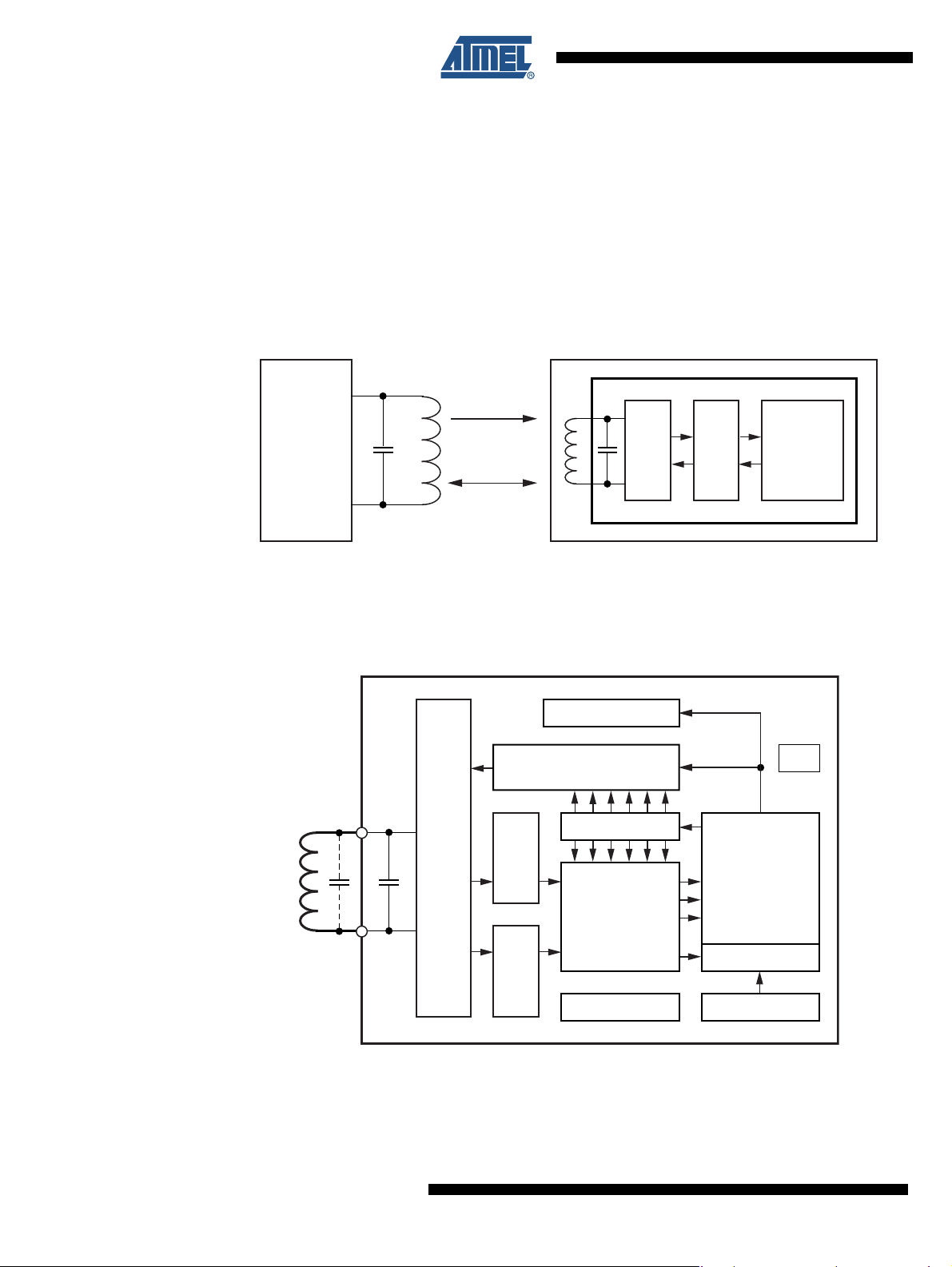
3. System Block Diagram
Figure 3-1. RFID System Using ATA5577 Tag
®
’s web site for product-relevant application notes.
4. ATA5577 - Functional Blocks
Figure 4-1. Block Diagram
2
ATA5577 [Preliminary]
4967DS–RFID–10/08
Page 3

4.1 Analog Front End (AFE)
The AFE includes all circuits that are directly connected to the coil terminals. It generates the
IC's power supply and handles the bi-directional data communication with the reader. It consists
of the following blocks:
• Rectifier to generate a DC supply voltage from the AC coil voltage
• Clock extractor
• Switchable load between Coil 1 and Coil 2 for data transmission from the tag to the reader
• Field-gap detector for data transmission from the base station to the tag
• ESD-protection circuitry
4.2 Data-rate Generator
The data rate is binary programmable to operate at any even-numbered data rate between RF/2
and RF/128 or to any of the fixed Basic mode data rates (RF/8, RF/16, RF/32, RF/40, RF/50,
RF/64, RF/100 and RF/128).
4.3 Write Decoder
The write decoder detects the write gaps and verifies the validity of the data stream according to
the Atmel e555x downlink protocol (pulse interval encoding).
ATA5577 [Preliminary]
4.4 HV Generator
This on-chip charge pump circuit generates the high voltage required to program the EEPROM.
4.5 DC Supply
Power is externally supplied to the IDIC via the two coil connections. The IC rectifies and regulates this RF source and uses it to generate its supply voltage.
4.6 Power-On Reset (POR)
The power-on reset circuit blocks the voltage supply to the IDIC until an acceptable voltage
threshold has been reached.
4.7 Clock Extraction
The clock extraction circuit uses the external RF signal as its internal clock source.
4.8 Controller
The control logic module executes the following functions:
• Load mode register with configuration data from EEPROM block 0 after power-on and during
reading
• Load option register with the settings for the analog front end stored in EEPROM page 1
block 3 after power-on and during reading
• Control all EEPROM memory read/write access and data protection
• Handles the downlink command decoding detecting protocol violations and error conditions
4967DS–RFID–10/08
3
Page 4

4.9 Mode Register
4.10 Modulator
4.11 Memory
The mode register maintains a readable shadow copy of the configuration data held in block 0 of
the EEPROM. It is continually refreshed during read mode and (re-)loaded after every POR
event or reset command. On delivery, the mode register is pre-programmed with default values
(see full version of the datasheet).
The modulator encodes the serialized EEPROM data for transmission to a tag reader or base
station. Several types of modulation are available including Manchester, bi-phase, FSK, PSK,
and NRZ.
Figure 4-2. Memory Map
0 1.........................................................................................32
L Analog front end option set-up Block 3
1 Traceability data Block 2
1 Traceability data Block 1
Page 1
L Page 0 configuration data Block 0
L User data or password Block 7
L User data Block 6
L User data Block 5
L User data Block 4
L User data Block 3
Page 0
L User data Block 2
L User data Block 1
L Configuration data Block 0
32 bits
Not transmitted
The memory is a 363-bit EEPROM, which is arranged in 11 blocks of 33 bits each. Each block
includes a single Lock bit, which is responsible for write-protecting the associated block. Programming takes place on a block basis, so a complete block (including lock bit) can be
programmed with a single command. The memory is subdivided into two page areas. Page 0
contains 8 blocks and page 1 contains 4 blocks. All 33 bits of a block, including the lock bit, are
programmed simultaneously.
4
ATA5577 [Preliminary]
4967DS–RFID–10/08
Page 5

ATA5577 [Preliminary]
Block 0 of page 0 contains the mode/configuration data, which is not transmitted during regular
read operations. Addressing block 0 will always affect block 0 of page 0 regardless of the page
selector. Block 7 of page 0 may be used as a write-protection password.
Block 3 of page 1 contains the option register, which is not transmitted during regular-read
operation.
Bit 0 of every block is the lock bit for that block. Once locked, the block (including the lock bit
itself) is not re-programmable via the RF field.
Blocks 1 and 2 of page 1 contain traceability data and are transmitted with the modulation
parameters defined in the configuration register after the opcode “11” is issued by the reader.
The traceability data blocks are programmed and locked by Atmel.
5. Absolute Maximum Ratings
Stresses beyond those listed under “Absolute Maximum Ratings” may cause permanent damage to the device. This is a stress rating
only and functional operation of the device at these or any other conditions beyond those indicated in the operational sections of this
specification is not implied. Exposure to absolute maximum rating conditions for extended periods may affect device reliability.
Parameters Symbol Value Unit
Maximum DC current into Coil1/Coil2 I
Maximum AC current into Coil1/Coil2, f = 125 kHz I
Power dissipation (die) (free-air condition, time of
application: 1s)
Electrostatic discharge maximum to
ANSI/ESD-STM5.1-2001 standard (HBM)
Operating ambient temperature range T
Storage temperature range (data retention
reduced)
coil p
P
V
T
coil
tot
max
amb
stg
20 (TBD) mA
20 (TBD) mA
100 (TBD) mW
2000 (TBD) V
–40 to +85 °C
–40 to +150 °C
4967DS–RFID–10/08
5
Page 6

6. Electrical Characteristics
T
= +25°C; f
amb
No. Parameters Test Conditions Symbol Min. Typ. Max. Unit Type*
1 RF frequency range f
2.1
2.2
2.3
3.1
3.2
3.3 Program EEPROM
4 Start-up time V
5.1
5.2 V
5.3 V
5.4
6.1
6.2 V
6.3 V
6.4
6.5 Thermal stability V
7.1
7.2 V
7.3 V
7.4
7.5 V
7.6 V
8 Programming time
9 Endurance Erase all/Write all
*) Type means: T: directly or indirectly tested during production; Q: guaranteed based on initial product qualification data
Notes: 1. IDD measurement set-up R = 100kΩ; V
2. Current into Coil1/Coil2 is limited to 10 mA.
3. Since EEPROM performance is influenced by assembly processes, Atmel confirms the parameters for DOW (tested die on
= 125 kHz; unless otherwise specified
coil
T
amb
Supply current (without
current consumed by the
external LC tank circuit)
Read - full temperature
range
Programming - full
temperature range
POR threshold (50-mV
hysteresis)
Coil voltage (AC supply)
Read mode and write
command
coil pp
Clamp voltage (depends
on settings in option
register)
3-mA current into
Coil1/Coil2
20-mA current into
Coil1/Coil2
3-mA current into
Modulation parameters
(depends on settings in
option register)
Coil1/Coil2 and
modulation ON
20 mA current into
Coil1/Coil2 and
modulation ON
Clock detection level
(depends on settings in
V
coil pp
option register)
Gap detection level
(depends on settings in
V
coil pp
option register)
From last command gap
to re-enter read mode
(64 + 648 internal
clocks)
defeat. I
DD
= (V
OUTmax
– V
CLK
uncut wafer) delivery.
= 25°C
(1)
(2)
(2)
= 6V t
= 8V
= 8 V
(3)
= V
CLK
coil
)/R
RF
100 125 150 kHz
1.5 TBD µA T
I
DD
2TBDµA Q
25 TBD µA Q
TBD 3.6 TBD V Q
V
coil pp
startup
V
pp clamp lo
pp clamp med
pp clamp hi
V
pp clamp med
V
pp mod lo
pp mod med
pp mod hi
V
pp mod med
mod lo/Tamb
V
clkdet lo
clkdet med
clkdet hi
V
gapdet lo
gapdet med
gapdet hi
T
prog
n
cycle
6V
8V
clamp
clamp
VQ
VQ
2.5 TBD ms Q
TBD 11 TBD V Q
TBD 13 TBD V Q
TBD 17 TBD V T
TBD 15 TBD V T
TBD 3 TBD V T
TBD 5 TBD V Q
TBD 7 TBD V Q
TBD 7.5 TBD V T
–1 mV/°C Q
TBD 250 TBD mV Q
TBD 550 TBD mV T
TBD 800 TBD mV Q
TBD 250 TBD mV Q
TBD 550 TBD mV T
TBD 850 TBD mV Q
55.76msT
100000 Cycles Q
= 3V: EEPROM programmed to 00 ... 000 (erase all); chip in modulation
6
ATA5577 [Preliminary]
4967DS–RFID–10/08
Page 7

ATA5577 [Preliminary]
6. Electrical Characteristics (Continued)
T
= +25°C; f
amb
No. Parameters Test Conditions Symbol Min. Typ. Max. Unit Type*
10.1
10.2 Top = 150°C
10.3 Top = 250°C
11.1
11.2 242 250 258
11.3 TBD 130 TBD
11.4 TBD 75 TBD
11.5 TBD 10 TBD Q
12.1
12.2 Temperature coefficient TBD TBD TBD TBD TBD TBD
*) Type means: T: directly or indirectly tested during production; Q: guaranteed based on initial product qualification data
Notes: 1. I
2. Current into Coil1/Coil2 is limited to 10 mA.
3. Since EEPROM performance is influenced by assembly processes, Atmel confirms the parameters for DOW (tested die on
= 125 kHz; unless otherwise specified
coil
Top = 55°C
Data retention
Resonance capacitor
Micromodule capacitor
parameters
measurement set-up R = 100kΩ; V
DD
defeat. I
DD
= (V
OUTmax
Mask option
V
coil pp
Capacitance tolerance
T
amb
– V
CLK
uncut wafer) delivery.
= 1V
)/R
(3)
(3)
(3)
t
retention
t
retention
t
retention
10 20 50 Years Q
96 hrs T
24 hrs Q
320 330 340
CLK
C
r
C
r
= V
= 3V: EEPROM programmed to 00 ... 000 (erase all); chip in modulation
coil
320 330 340 pF T
pF
T
7. Revision History
Please note that the following page numbers referred to in this section refer to the specific revision
mentioned, not to this document.
Revision No. History
4967DS-RFID-10/08 • Features on page 1 changed
4967CS-RFID-01/08
4967BS-RFID-09/07
• Features on page 1 changed
• Section 2 “Compatibility” on page 2 changed
• Section 4.9 “Mode Register” on page 4 changed
• Put datasheet in a new template
• Section 4.2 “Data-rate Generator” on page 3 changed
• Figure 4-2 “Memory Map” on page 5 changed
• Section 6 “Electrical Characteristics” numbers 2.1, 2.2 and 2.3 on page 6
changed
4967DS–RFID–10/08
7
Page 8

Headquarters International
Atmel Corporation
2325 Orchard Parkway
San Jose, CA 95131
USA
Tel: 1(408) 441-0311
Fax: 1(408) 487-2600
Atmel Asia
Room 1219
Chinachem Golden Plaza
77 Mody Road Tsimshatsui
East Kowloon
Hong Kong
Tel: (852) 2721-9778
Fax: (852) 2722-1369
Product Contact
Web Site
www.atmel.com
Literature Requests
www.atmel.com/literature
Atmel Europe
Le Krebs
8, Rue Jean-Pierre Timbaud
BP 309
78054
Saint-Quentin-en-Yvelines Cedex
France
Tel: (33) 1-30-60-70-00
Fax: (33) 1-30-60-71-11
Technical Support
rfid@atmel.com
Atmel Japan
9F, Tonetsu Shinkawa Bldg.
1-24-8 Shinkawa
Chuo-ku, Tokyo 104-0033
Japan
Tel: (81) 3-3523-3551
Fax: (81) 3-3523-7581
Sales Contact
www.atmel.com/contacts
Disclaimer: The information in this document is provided in connection with Atmel products. No license, express or implied, by estoppel or otherwise, to any
intellectual property right is granted by this document or in connection with the sale of Atmel products. EXCEPT AS SET FORTH IN ATMEL’S TERMS AND CONDI-
TIONS OF SALE LOCATED ON ATMEL’S WEB SITE, ATMEL ASSUMES NO LIABILITY WHATSOEVER AND DISCLAIMS ANY EXPRESS, IMPLIED OR STATUTORY
WARRANTY RELATING TO ITS PRODUCTS INCLUDING, BUT NOT LIMITED TO, THE IMPLIED WARRANTY OF MERCHANTABILITY, FITNESS FOR A PARTICULAR
PURPOSE, OR NON-INFRINGEMENT. IN NO EVENT SHALL ATMEL BE LIABLE FOR ANY DIRECT, INDIRECT, CONSEQUENTIAL, PUNITIVE, SPECIAL OR INCIDENTAL DAMAGES (INCLUDING, WITHOUT LIMITATION, DAMAGES FOR LOSS OF PROFITS, BUSINESS INTERRUPTION, OR LOSS OF INFORMATION) ARISING OUT OF
THE USE OR INABILITY TO USE THIS DOCUMENT, EVEN IF ATMEL HAS BEEN ADVISED OF THE POSSIBILITY OF SUCH DAMAGES. Atmel makes no
representations or warranties with respect to the accuracy or completeness of the contents of this document and reserves the right to make changes to specifications
and product descriptions at any time without notice. Atmel does not make any commitment to update the information contained herein. Unless specifically provided
otherwise, Atmel products are not suitable for, and shall not be used in, automotive applications. Atmel’s products are not intended, authorized, or warranted for use
as components in applications intended to support or sustain life.
© 2008 Atmel Corporation. All rights reserved. Atmel®, logo and combinations thereof, IDIC® and others are registered trademarks or trade-
marks of Atmel Corporation or its subsidiaries. Other terms and product names may be trademarks of others.
4967DS–RFID–10/08
 Loading...