

Page 1

Features
• Contactless Power Supply
• Contactless Read/Write Data Transmission
• Radio Frequency f
• 128-bit EEPROM User Memory: 16 Bytes (8 Bits Each)
• 8-bit Configuration Memory
• High Q-antenna Tolerance Due to Built-in Options
• Applications
– Access Control
• Standard Unique Format (Manchester, RF/64)
• 40-bitData Memory
• 14-bit Parity Memory
• 9-bit Header Memory
• On-chip Trimmed Antenna Capacitor
– 330 pF ±3%
– 250 pF ±3%
• Mega Pads 200 µm × 400 µm
• Mega Pads 200 µm × 400 µm with 25 µm Gold Bumps for Direct Coil Bonding
• Other Options:
– Direct Access Mode
– OTP Functionality
from 100 kHz to 150 kHz
RF
1. Description
The ATA5575 is a contactless read/write identification IC (IDIC®) for applications in
the 100-kHz to 150-kHz frequency band. A single coil connected to the chip serves as
the IC’s power supply and bi-directional communication interface. The antenna and
chip together form a transponder or tag.
Read/Write
LF RFID IDIC
100 kHz to
150 kHz
ATA5575M1
Summary
Preliminary
The on-chip 128-bit user EEPROM (16 bytes with 8 bits each) can be read and written
byte-wise from a base station (reader). Data is transmitted from the IDIC (uplink) using
load modulation. This is achieved by damping the RF field with a resistive load
between the two terminals Coil 1 and Coil 2. The IC receives and decodes serial base
station commands (downlink), which are encoded as 100% amplitude modulated
(OOK) pulse-interval-encoded bit streams.
The ATA5575 is an EEPROM-based circuit. It is optimized for maximum read range.
Programming is also possible, but the write range is limited.
The chip has to be locked after loading the application-specific data into the device.
Until the enable bits are set properly, the ATA5575M1 transmits all digits “0” in unique
format. Typical applications run at 125 kHz.
NOTE: This is a summary document.
The complete document is available.
For more information, please contact
your local Atmel sales office.
9167AS–RFID–11/09
Page 2
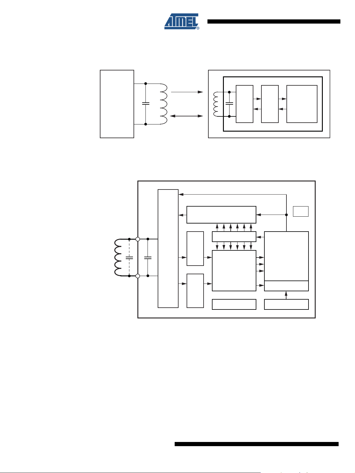
2. System Block Diagram
Data
Reader
or
Base station
ATA5575
Power
Tr ansponder
Coil interface
Controller
Memory
Memory
(136-bit EEPROM)
Modulator
Analog front end
Data-rate
generator
Write
decoder
POR
Coil 2
Coil 1
Controller
Te st logic HV generator
Input register
Mode register
Figure 2-1. RFID System Using ATA5575 Tag
3. ATA5575 - Functional Blocks
Figure 3-1. Block Diagram
2
ATA5575M1 [Preliminary]
9167AS–RFID–11/09
Page 3

4. Analog Front End (AFE)
The AFE includes all circuits which are directly connected to the coil terminals, it generates the
IC’s power supply and handles the bi-directional data communication with the reader. The
AFE consists of the following blocks:
• Rectifier to generate a DC supply voltage from the AC coil voltage
• Clock extractor
• Switchable load between Coil 1 and Coil 2 for data transmission from tag to the reader
• Field-gap detector for data transmission from the base station to the tag
• ESD protection circuitry
4.1 Data Rate Generator
The data rate is fixed to RF/64.
4.2 Write Decoder
The write decoder detects the write gaps and verifies the validity of the data stream according
to the Atmel
ATA5575M1 [Preliminary]
®
downlink protocol (pulse interval encoding).
4.3 HV Generator
This on-chip charge pump circuit generates the high voltage required for programming the
EEPROM.
4.4 DC Supply
Power is externally supplied to the IDIC via the two coil connections. The IC rectifies and regulates this RF source and uses it to generate its supply voltage.
4.5 Power-On Reset (POR)
The power-on reset circuit blocks the voltage supply to the IDIC until an acceptable voltage
threshold has been reached. This, in turn, triggers the default initialization delay sequence.
During this configuration period of 98 field clocks, the ATA5575 is initialized with the configuration data stored in EEPROM byte 16.
4.6 Clock Extraction
The clock extraction circuit uses the external RF signal as its internal clock source.
4.7 Controller
The control logic module executes the following functions:
• Load mode register with configuration data from EEPROM byte 16 after power-on and
during reading
• Controls each EEPROM memory read/write access and handles the data protection
• Handle the downlink command decoding, detecting protocol violations and error conditions
9167AS–RFID–11/09
3
Page 4

4.8 Mode Register
4.9 Modulator
4.10 Memory
The mode register maintains a readable shadow copy of the configuration data held in byte 16
of the EEPROM. It is continually refreshed during read mode and (re-)loaded after every POR
event or reset command. Depending on the version, the configuration data is pre-programmed
when leaving Atmel’s production.
The modulator encodes the serialized EEPROM data for transmission to a tag reader or a
base station. Modulation available: Manchester.
Figure 4-1. Memory Map
1………………....…………….8
Configuration Data Byte 16
User Data Byte 15
User Data Byte 14
User Data Byte 13
User Data Byte 12
User Data Byte 11
User Data Byte 10
User Data Byte 9
User Data Byte 8
User Data Byte 7
User Data Byte 6
User Data Byte 5
User Data Byte 4
User Data Byte 3
User Data Byte 2
User Data Byte 1
User Data Byte 0
8 bits
Not transmitted
The memory is a 136-bit EEPROM, which is arranged in 17 bytes of 8 bits each. Programming
is carried out byte-wise, so a complete byte will be programmed with a single command.
Byte 16 contains the mode/configuration data, which is not transmitted during regular read
operations.
A special bit combination in byte 16 will lock the entire memory. Once locked, the memory
(including byte 16 itself) can not be re-programmed once more via the RF field.
4
ATA5575M1 [Preliminary]
9167AS–RFID–11/09
Page 5

ATA5575M1 [Preliminary]
5. Absolute Maximum Ratings
Stresses beyond those listed under “Absolute Maximum Ratings” may cause permanent damage to the device. This is a stress rating
only and functional operation of the device at these or any other conditions beyond those indicated in the operational sections of this
specification is not implied. Exposure to absolute maximum rating conditions for extended periods may affect device reliability.
Parameters Symbol Value Unit
Maximum DC current into Coil1/Coil2 I
Maximum AC current into Coil1/Coil2
f = 125 kHz
Power dissipation (dice) (free-air condition, time of
application: 1s)
Electrostatic discharge maximum to ANSI/ESD-STM5.1-2001
standard (HBM)
Operating ambient temperature range T
Storage temperature range (data retention reduced) T
I
coil p
P
V
coil
tot
max
amb
stg
t
6. Electrical Characteristics
T
= +25°C; f
amb
No. Parameters Test Conditions Symbol Min. Typ. Max. Unit Type*
1 RF frequency range f
Supply current
(without current
2.1
consumed by the external
LC tank circuit)
2.2
2.3
3.1
Coil voltage (AC supply)
3.2 Program EEPROM
4 Start-up time V
5.1
Clamp
5.2 20 mA current into Coil1/2 V
6.1
Modulation parameters
6.2
6.3 Thermal stability V
*) Type means: T: directly or indirectly tested during production; Q: guaranteed based on initial product qualification data
Notes: 1. I
2. Current into Coil1/Coil2 is limited to 10 mA.
3. Since the EEPROM performance is influenced by assembly processes, Atmel can not confirm the parameters for -DDW
= 125 kHz; unless otherwise specified
coil
100 125 150 kHz
T
amb
= 25°C
RF
(1)
I
DD
Read – full temperature
range
Programming – full
temperature range
Read mode and write
command
coil pp
3 mA current into Coil1/2 V
3 mA current into Coil1/2
and modulation ON
20 mA current into Coil1/2
and modulation ON
measurement setup: EEPROM programmed to 00 ... 000 (erase all); chip in modulation defeat.
DD
(2)
(2)
= 6V t
mod lo /Tamb
V
coil pp
startup
V
V
pp
pp
pp
pp
6V
16 V
TBD 17 TBD V T
TBD 20 TBD V T
TBD 7 TBD V Q
TBD 9 TBD V T
(tested die on unsawn wafer) delivery.
TBD mA
TBD mA
TBD mW
TBD V
–40 to +85 °C
–40 to +150 °C
1.5 3 µA T
25µAQ
25 µA Q
clamp
clamp
VQ
VQ
1.1 ms Q
–1 mV/°C Q
9167AS–RFID–11/09
5
Page 6

6. Electrical Characteristics (Continued)
T
= +25°C; f
amb
No. Parameters Test Conditions Symbol Min. Typ. Max. Unit Type*
7.1 Clock detection level V
7.2 Gap detection level V
8 Programming time
9 Endurance Erase all / write all
10.1
10.2 Top = 150°C
Data retention
10.3 Top = 250°C
11.1
Resonance capacitor
11.2 TBD 250 TBD
*) Type means: T: directly or indirectly tested during production; Q: guaranteed based on initial product qualification data
Notes: 1. I
2. Current into Coil1/Coil2 is limited to 10 mA.
3. Since the EEPROM performance is influenced by assembly processes, Atmel can not confirm the parameters for -DDW
= 125 kHz; unless otherwise specified
coil
= 8V V
coil pp
= 8V V
coil pp
clkdet
gapdet med
TBD 550 TBD mV T
TBD 550 TBD mV T
From last command gap
to re-enter read mode
T
prog
55.76msT
(64 + 648 internal clocks)
(3)
Top = 55°C
Mask option
V
coil pp
measurement setup: EEPROM programmed to 00 ... 000 (erase all); chip in modulation defeat.
DD
(3)
(3)
(3)
(4)
= 1V
n
cycle
t
retention
t
retention
t
retention
C
100000 Cycles Q
10 20 50 Years Q
96 hrs T
24 hrs Q
TBD 330 TBD
r
(tested die on unsawn wafer) delivery.
pF T
6
ATA5575M1 [Preliminary]
9167AS–RFID–11/09
Page 7

Headquarters International
Atmel Corporation
2325 Orchard Parkway
San Jose, CA 95131
USA
Tel: 1(408) 441-0311
Fax: 1(408) 487-2600
Atmel Asia
Unit 1-5 & 16, 19/F
BEA Tower, Millennium City 5
418 Kwun Tong Road
Kwun Tong, Kowloon
Hong Kong
Tel: (852) 2245-6100
Fax: (852) 2722-1369
Product Contact
Web Site
www.atmel.com
Literature Requests
www.atmel.com/literature
Atmel Europe
Le Krebs
8, Rue Jean-Pierre Timbaud
BP 309
78054
Saint-Quentin-en-Yvelines Cedex
France
Tel: (33) 1-30-60-70-00
Fax: (33) 1-30-60-71-11
Technical Support
rfid@atmel.com
Atmel Japan
9F, Tonetsu Shinkawa Bldg.
1-24-8 Shinkawa
Chuo-ku, Tokyo 104-0033
Japan
Tel: (81) 3-3523-3551
Fax: (81) 3-3523-7581
Sales Contact
www.atmel.com/contacts
Disclaimer: The information in this document is provided in connection with Atmel products. No license, express or implied, by estoppel or otherwise, to any
intellectual property right is granted by this document or in connection with the sale of Atmel products. EXCEPT AS SET FORTH IN ATMEL’S TERMS AND CONDI-
TIONS OF SALE LOCATED ON ATMEL’S WEB SITE, ATMEL ASSUMES NO LIABILITY WHATSOEVER AND DISCLAIMS ANY EXPRESS, IMPLIED OR STATUTORY
WARRANTY RELATING TO ITS PRODUCTS INCLUDING, BUT NOT LIMITED TO, THE IMPLIED WARRANTY OF MERCHANTABILITY, FITNESS FOR A PARTICULAR
PURPOSE, OR NON-INFRINGEMENT. IN NO EVENT SHALL ATMEL BE LIABLE FOR ANY DIRECT, INDIRECT, CONSEQUENTIAL, PUNITIVE, SPECIAL OR INCIDENTAL DAMAGES (INCLUDING, WITHOUT LIMITATION, DAMAGES FOR LOSS OF PROFITS, BUSINESS INTERRUPTION, OR LOSS OF INFORMATION) ARISING OUT OF
THE USE OR INABILITY TO USE THIS DOCUMENT, EVEN IF ATMEL HAS BEEN ADVISED OF THE POSSIBILITY OF SUCH DAMAGES. Atmel makes no
representations or warranties with respect to the accuracy or completeness of the contents of this document and reserves the right to make changes to specifications
and product descriptions at any time without notice. Atmel does not make any commitment to update the information contained herein. Unless specifically provided
otherwise, Atmel products are not suitable for, and shall not be used in, automotive applications. Atmel’s products are not intended, authorized, or warranted for use
as components in applications intended to support or sustain life.
© 2009 Atmel Corporation. All rights reserved. Atmel®, logo and combinations thereof, IDIC® and others are registered trademarks or trade-
marks of Atmel Corporation or its subsidiaries. Other terms and product names may be trademarks of others.
9167AS–RFID–11/09
 Loading...