

Page 1
Features
• Low-Voltage and Standard-Voltage Operation
–2.7(V
–2.5(V
• 3-Wire Serial Interface
• Schmitt Trigger, Filtered Inputs for Noise Suppression
• 2MHzClockRate(5V)
• Self-Timed Write Cycle (10 ms max)
• High Reliability
– Endurance: 1 Million Write Cycles
– Data Retention: 100 Years
• Automotive Grade and Extended Temperature Devices Available
• 8-lead PDIP and 8-lead JEDEC SOIC Packages
=2.7Vto5.5V)
CC
=2.5Vto5.5V)
CC
3-Wire
Serial EEPROM
Description
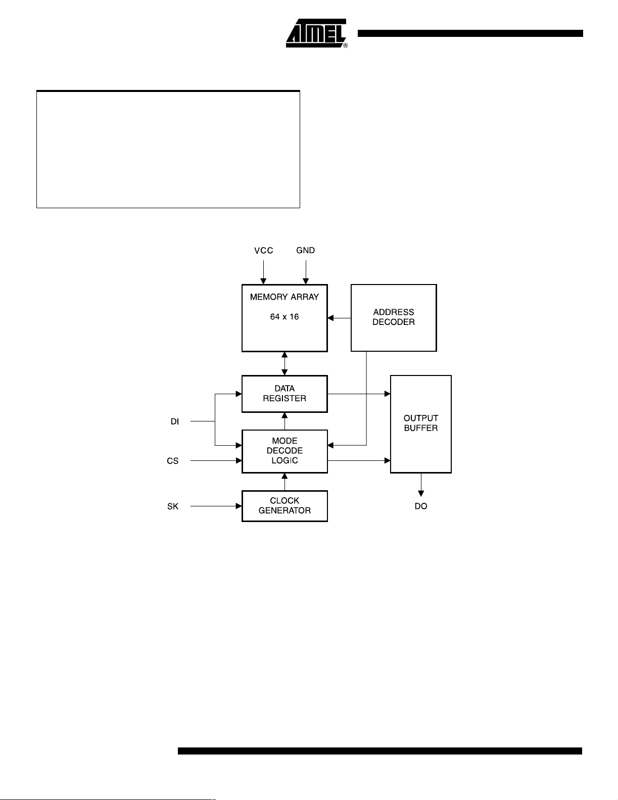
The AT93C46C provides 1024 bits of serial electrically-erasable programmable read
only memory (EEPROM) organized as 64 words of 16 bits each. The device is optimized for use in many industrial and commercial applications where low-power and
low-voltage operation are essential. The AT93C46C is available in space saving 8lead PDIP and 8-lead JEDEC SOIC packages.
TheAT93C46CisenabledthroughtheChipSelectpin(CS),andaccessedviaa3wire serial interface consisting of Data Input (DI), Data Output (DO), and Shift Clock
(SK). Upon receiving a READ instruction at DI, the address is decoded and the data is
clocked out serially on the data output pin DO. The WRITE cycle is completely selftimed and no separate ERASE cycle is required before WRITE. The WRITE cycle is
only enabled when the part is in the ERASE/WRITE ENABLE state. When CS is
brought “high” following the initiation of a WRITE cycle, the DO pin outputs the
READY/BUSY status of the part.
The AT93C46C is available in 2.7V to 5.5V and 2.5V to 5.5V versions.
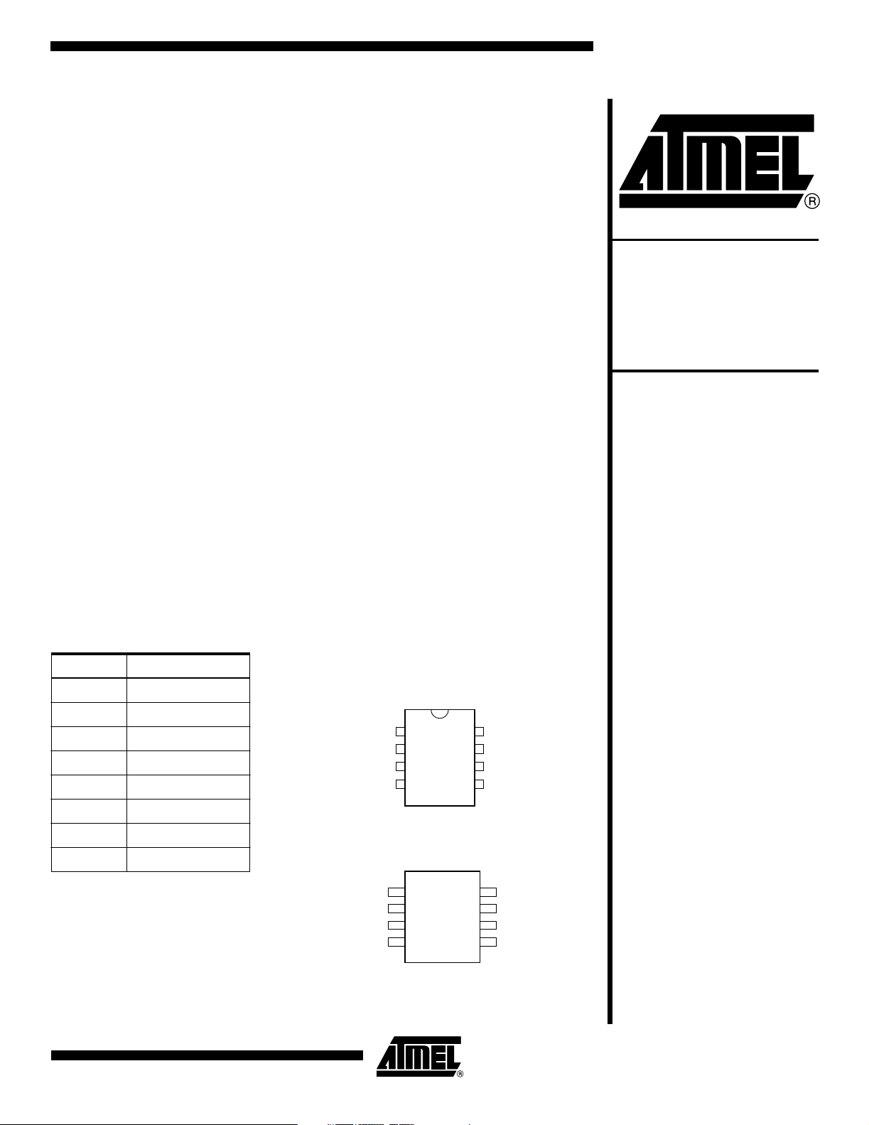
Pin Configurations
Pin Name Function
CS Chip Select
SK Serial Data Clock
DI Serial Data Input
DO Serial Data Output
GND Ground
CS
SK
DI
DO
8-lead PDIP
1
2
3
4
8
7
6
5
VCC
DC
NC
GND
1K (64 x 16)
AT93C46C
VCC Power Supply
NC No Connect
DC Don’t Connect
CS
SK
DO
DI
8-lead SOIC
1
2
3
4
VCC
8
DC
7
NC
6
GND
5
Rev. 1122D–SEEPR–08/02
1
Page 2
Absolute Maximum Ratings*
Operating Temperature .................................. -55°Cto+125°C
Storage Temperature ..................................... -65°Cto+150°C
Voltage on Any Pin
with Respect to Ground .....................................-1.0V to +7.0V
Maximum Operating Voltage .......................................... 6.25V
DC Output Current ........................................................ 5.0 mA
Block Diagram
*NOTICE: Stresses beyond those listed under “Absolute
Maximum Ratings” may cause permanent damage to the device. This is a stress rating only and
functional operation of the device at these or any
other conditions beyond those indicated in the
operational sections of this specification is not
implied. Exposure to absolute maximum rating
conditions for extended periods may affect
device reliability.
2
AT93C46C
1122D–SEEPR–08/02
Page 3
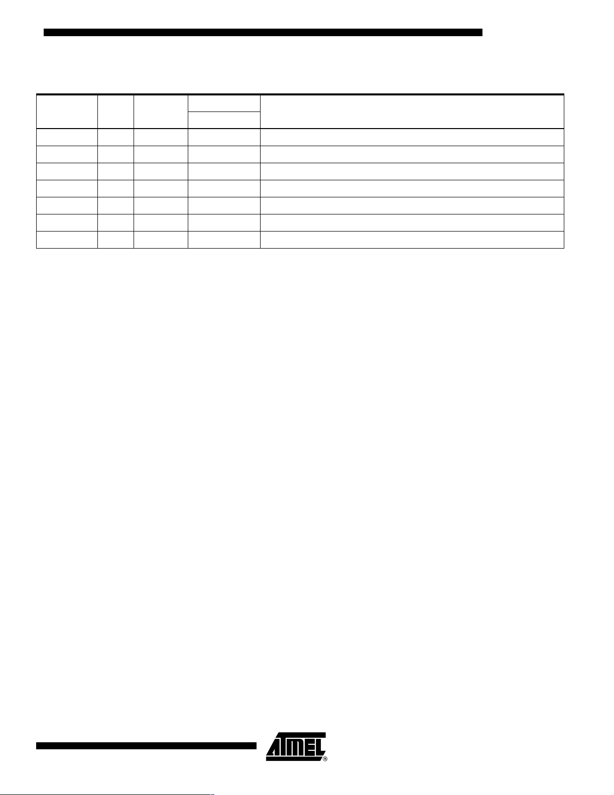
AT93C46C
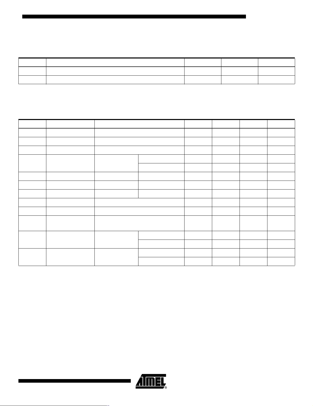
Pin Capacitance
(1)
Applicable over recommended operating range from TA=25°C, f = 1.0 MHz, VCC= +5.0V (unless otherwise noted).
Symbol Test Conditions Max Units Conditions
C
OUT
C
IN
Output Capacitance (DO) 5 pF V
OUT
=0V
Input Capacitance (CS, SK, DI) 5 pF VIN=0V
Note: 1. This parameter is characterized and is not 100% tested.
DC Characteristics
Applicable over recommended operating range from: TAI=-40°Cto+85°C, VCC= +2.5V to +5.5V,
T
=0°Cto+70°C, VCC= +2.5V to +5.5V (unless otherwise noted).
AC
Symbol Parameter Test Condition Min Typ Max Units
V
CC1
V
CC2
V
CC3
I
CC
I
SB1
I
SB2
I
SB3
I
IL
I
OL
(1)
V
IL1
(1)
V
IH1
V
OL1
V
OH1
V
OL2
V
OH2
Note: 1. V
Supply Voltage 2.5 5.5 V
Supply Voltage 2.7 5.5 V
Supply Voltage 4.5 5.5 V
READ at 1.0 MHz 0.5 2.0 mA
Supply Current VCC=5.0V
WRITE at 1.0 MHz 0.5 2.0 mA
Standby Current VCC= 2.5V CS = 0V 14.0 20.0 µA
Standby Current VCC= 2.7V CS = 0V 14.0 20.0 µA
Standby Current VCC= 5.0V CS = 0V 35.0 50.0 µA
Input Leakage VIN=0VtoV
Output Leakage VIN=0VtoV
Input Low Voltage
Input High Voltage
Output Low Voltage
Output High Voltage
Output Low Voltage
Output High Voltage
min and VIHmax are reference only and are not tested.
IL
2.5V ≤ V
4.5V ≤ V
2.5V ≤ V
CC
CC
CC
CC
CC
≤ 5.5V
≤ 5.5V
≤ 2.7V
I
=2.1mA 0.4 V
OL
I
=-0.4mA 2.4 V
OH
=0.15mA 0.2 V
I
OL
I
=-100µAV
OH
-0.6
x0.7
V
CC
-0.2 V
CC
0.1 1.0 µA
0.1 1.0 µA
V
x0.3
CC
+1
V
CC
V
1122D–SEEPR–08/02
3
Page 4
AC Characteristics
Applicable over recommended operating range from TA=-40°Cto+85°C, VCC=+2.5Vto+5.5V,
CL = 1 TTL Gate and 100 pF (unless otherwise noted).
Symbol Parameter Test Condition Min Typ Max Units
f
SK
t
SKH
t
SKL
t
CS
t
CSS
SK Clock Frequency 4.5V ≤ VCC ≤ 5.5V
2.7V ≤ V
2.5V ≤ V
CC
CC
≤ 5.5V
≤ 5.5V
SK High Time 4.5V ≤ VCC ≤ 5.5V
2.7V ≤ V
2.5V ≤ V
CC
CC
≤ 5.5V
≤ 5.5V
SK Low Time 4.5V ≤ VCC ≤ 5.5V
2.7V ≤ V
2.5V ≤ V
CC
CC
≤ 5.5V
≤ 5.5V
Minimum CS Low Time 4.5V ≤ VCC ≤ 5.5V
2.7V ≤ V
2.5V ≤ V
CC
CC
≤ 5.5V
≤ 5.5V
CS Setup Time
Relative to SK
t
DIS
DI Setup Time
Relative to SK
t
CSH
t
DIH
CS Hold Time Relative to SK 0 ns
DI Hold Time
Relative to SK
t
PD1
Output Delay to ‘1’
AC Test
t
PD0
Output Delay to ‘0’
AC Test
t
SV
CS to Status Valid
AC Test
t
DF
t
WP
Endurance
CS to DO in High Impedance
AC Test
CS = V
IL
Write Cycle Time 10 ms
5.0V, 25°C, Page Mode
(1)
Note: 1. This parameter is characterized and is not 100% tested.
4.5V ≤ VCC ≤ 5.5V
2.7V ≤ V
2.5V ≤ V
CC
CC
≤ 5.5V
≤ 5.5V
4.5V ≤ VCC ≤ 5.5V
2.7V ≤ V
2.5V ≤ V
CC
CC
≤ 5.5V
≤ 5.5V
4.5V ≤ VCC ≤ 5.5V
2.7V ≤ V
2.5V ≤ V
CC
CC
≤ 5.5V
≤ 5.5V
4.5V ≤ VCC ≤ 5.5V
2.7V ≤ V
2.5V ≤ V
CC
CC
≤ 5.5V
≤ 5.5V
4.5V ≤ VCC ≤ 5.5V
2.7V ≤ V
2.5V ≤ V
CC
CC
≤ 5.5V
≤ 5.5V
4.5V ≤ VCC ≤ 5.5V
2.7V ≤ V
2.5V ≤ V
CC
CC
≤ 5.5V
≤ 5.5V
4.5V ≤ VCC ≤ 5.5V
2.7V ≤ V
2.5V ≤ V
4.5V ≤ V
≤ 5.5V
CC
≤ 5.5V
CC
≤ 5.5V 3 ms
CC
0
0
0
250
250
500
250
250
500
250
250
500
50
50
100
100
100
200
100
100
200
1M
2
1
0.5
250
250
500
250
250
500
250
250
500
100
100
200
MHz
ns
ns
ns
ns
ns
ns
ns
ns
ns
ns
Write
Cycle
4
AT93C46C
1122D–SEEPR–08/02
Page 5
Instruction Set for the AT93C46C
Address
AT93C46C
Instruction SB Op Code
READ 1 10 A
EWEN 1 00 11XXXX Write enable must precede all programming modes.
ERASE 1 11 A
WRITE 1 01 A
ERAL 1 00 10XXXX Erases all memory locations. Valid only at V
WRAL 1 00 01XXXX Writes all memory locations. Valid only at V
EWDS 1 00 00XXXX Disables all programming instructions.
Functional Description
5-A0
5-A0
5-A0
The AT93C46C is accessed via a simple and versatile three-wire serial communication
interface. Device operation is controlled by seven instructions issued by the host processor. A valid instruction starts with a rising edge of CS and consists of a Start Bit
Commentsx16
Reads data stored in memory, at specified address.
Erase memory location An-A0.
Writes memory location An-A0.
(logic “1”) followed by the appropriate Op Code and the desired memory Address
location.
READ (READ): The Read (READ) instruction contains the Address code for the memory location to be read. After the instruction and address are decoded, data from the
selected memory location is available at the serial output pin DO. Output data changes
are synchronized with the rising edges of serial clock SK. It should be noted that a
dummy bit (logic “0”) precedes the 16-bit data output string.
ERASE/WRITE (EWEN): To assure data integrity, the part automatically goes into the
Erase/Write Disable (EWDS) state when power is first applied. An Erase/Write Enable
(EWEN) instruction must be executed first before any programming instructions can be
carried out. Please note that once in the Erase/Write Enable state, programming
remains enabled until an Erase/Write Disable (EWDS) instruction is executed or V
power is removed from the part.
= 4.5V to 5.5V.
CC
= 4.5V to 5.5V.
CC
CC
1122D–SEEPR–08/02
ERASE (ERASE): The Erase (ERASE) instruction programs all bits in the specified
memory location to the logical “1” state. The self-timed erase cycle starts once the
ERASE instruction and address are decoded. The DO pin outputs the READY/BUSY
status of the part if CS is brought high after being kept low for a minimum of 250 ns (t
CS
A logic “1” at pin DO indicates that the selected memory location has been erased, and
the part is ready for another instruction.
WRITE (WRITE): The Write (WRITE) instruction contains the 16 bits of data to be written into the specified memory location. The self-timed programming cycle t
WP
starts
after the last bit of data is received at serial data input pin DI. The DO pin outputs the
READY/BUSY status of the part if CS is brought high after being kept low for a minimum
of 250 ns (t
). A logic “0” at DO indicates that programming is still in progress. A logic
CS
“1” indicates that the memory location at the specified address has been written with the
data pattern contained in the instruction and the part is ready for further instructions. A
Ready/Busy Status cannot be obtained if the CS is brought high after the end of
the self-timed programming cycle, t
WP
.
).
5
Page 6

ERASE ALL (ERAL): The Erase All (ERAL) instruction programs every bit in the
memory array to the logic “1” state and is primarily used for testing purposes. The DO
pin outputs the READY/BUSY status of the part if CS is brought high after being kept
low for a minimum of 250 ns (t
). The ERAL instruction is valid only at VCC=5.0V±
CS
10%.
WRITE ALL (WRAL): The Write All (WRAL) instruction programs all memory locations with the data patterns specified in the instruction. The DO pin outputs the
READY/BUSY status of the part if CS is brought high after being kept low for a minimum
of 250 ns (t
). The WRAL instruction is valid only at VCC=5.0V± 10%.
CS
ERASE/WRITE DISABLE (EWDS): To protect against accidental data disturb, the
Erase/Write Disable (EWDS) instruction disables all programming modes and should be
executed after all programming operations. The operation of the READ instruction is
independent of both the EWEN and EWDS instructions and can be executed at any
time.
6
AT93C46C
1122D–SEEPR–08/02
Page 7

Timing Diagrams
Synchronous Data Timing
AT93C46C
Note: This is the minimum SK period.
1122D–SEEPR–08/02
7
Page 8

Organization Key for Timing Diagrams
AT93C46C
READ Timing
EWEN Timing
(1)
CS
I/O
A
D
x16
N
N
High Impedance
t
CS
A
5
D
15
t
CS
SK
DI
001
Note: 1. Requires a minimum of nine clock cycles.
EWDS Timing
(1)
CS
SK
DI 1 0
000
Note: 1. Requires a minimum of nine clock cycles.
11
...
t
CS
...
8
AT93C46C
1122D–SEEPR–08/02
Page 9

WRITE Timing
CS
SK
AT93C46C
t
CS
WRAL Timing
(1)(2)
DI
DO
HIGH IMPEDANCE
11
CS
SK
DI
DO
1 0 0 1 ... D
HIGH IMPEDANCE
Notes: 1. Valid only at VCC= 4.5V to 5.5V.
2. Requires a minimum of nine clock cycles.
... ...
0A0D0
A
N
D
N
BUSY
t
WP
t
CS
... D00
N
t
WP
READY
BUSY
READY
1122D–SEEPR–08/02
9
Page 10

ERASE Timing
t
CS
ERAL Timing
CS
SK
DI A
HIGH IMPEDANCE
DO
1 1 ...1
(1)
CS
SK
DI 1 1000
N
A
N-1AN-2
A0
READY
STANDBY
t
DF
HIGH IMPEDANCE
STANDBY
CHECK
STATUS
t
SV
BUSY
t
WP
t
CS
CHECK
STATUS
HIGH IMPEDANCE
DO
Note: 1. Valid only at VCC= 4.5V to 5.5V.
t
SV
BUSY
READY
t
WP
t
DF
HIGH IMPEDANCE
10
AT93C46C
1122D–SEEPR–08/02
Page 11

AT93C46C
Ordering Information
Ordering Code Package Operation Range
AT93C46C-10PI-2.7
AT93C46C-10SI-2.7
AT93C46C-10PI-2.5
AT93C46C-10SI-2.5
Note: For 2.7V and 2.5V devices used in the 4.5V to 5.5V range, please refer to performance values in the AC and DC characteristics
table.
8P3
8S1
8P3
8S1
Industrial
(-40°Cto85°C)
Industrial
(-40°Cto85°C)
Package Type
8P3 8-lead, 0.300" Wide, Plastic Dual Inline Package (PDIP)
8S1 8-lead, 0.150" Wide, Plastic Gull Wing Small Outline (JEDEC SOIC)
Options
-2.7 Low Voltage (2.7V to 5.5V)
-2.5 Low Voltage (2.5V to 5.5V)
1122D–SEEPR–08/02
11
Page 12

Packaging Information
8P3 – PDIP
D1
b3
4 PLCS
Top View
D
e
Side View
1
E
E1
N
c
eA
End View
COMMON DIMENSIONS
(Unit of Measure = inches)
b
b2
A2 A
SYMBOL
A 0.210 2
A2 0.115 0.130 0.195
b 0.014 0.018 0.022 5
b2 0.045 0.060 0.070 6
b3 0.030 0.039 0.045 6
c 0.008 0.010 0.014
D 0.355 0.365 0.400 3
L
D1 0.005 3
E 0.300 0.310 0.325 4
E1 0.240 0.250 0.280 3
e 0.100 BSC
eA 0.300 BSC 4
L 0.115 0.130 0.150 2
MIN
NOM
MAX
NOTE
Notes: 1. This drawing is for general information only; refer to JEDEC Drawing MS-001, Variation BA for additional information.
12
2. Dimensions A and L are measured with the package seated in JEDEC seating plane Gauge GS-3.
3. D, D1 and E1 dimensions do not include mold Flash or protrusions. Mold Flash or protrusions shall not exceed 0.010 inch.
4. E and eA measured with the leads constrained to be perpendicular to datum.
5. Pointed or rounded lead tips are preferred to ease insertion.
6. b2 and b3 maximum dimensions do not include Dambar protrusions. Dambar protrusions shall not exceed 0.010 (0.25 mm).
TITLE
2325 Orchard Parkway
R
San Jose, CA 95131
8P3, 8-lead, 0.300" Wide Body, Plastic Dual
In-line Package (PDIP)
AT93C46C
DRAWING NO.
8P3
1122D–SEEPR–08/02
01/09/02
REV.
B
Page 13

8S1 – JEDEC SOIC
Top View
AT93C46C
1
2
3
H
N
A2
L
e
D
Side View
E
End View
B
A
COMMON DIMENSIONS
(Unit of Measure = mm)
SYMBOL
A – – 1.75
B – – 0.51
C
C – – 0.25
D – – 5.00
E – – 4.00
e 1.27 BSC
H – – 6.20
L – – 1.27
MIN
NOM
MAX
NOTE
Note:
This drawing is for general information only. Refer to JEDEC Drawing MS-012 for proper dimensions, tolerances, datums, etc.
2325 Orchard Parkway
R
San Jose, CA 95131
1122D–SEEPR–08/02
TITLE
8S1, 8-lead (0.150" Wide Body), Plastic Gull Wing
Small Outline (JEDEC SOIC)
DRAWING NO.
8S1 A
10/10/01
REV.
13
Page 14

Atmel Headquarters Atmel Operations
Corporate Headquarters
2325 Orchard Parkway
San Jose, CA 95131
TEL 1(408) 441-0311
FAX 1(408) 487-2600
Europe
Atmel Sarl
Route des Arsenaux 41
Case Postale 80
CH-1705 Fribourg
Switzerland
TEL (41) 26-426-5555
FAX (41) 26-426-5500
Asia
Room 1219
Chinachem Golden Plaza
77 Mody Road Tsimshatsui
East Kowloon
Hong Kong
TEL (852) 2721-9778
FAX (852) 2722-1369
Japan
9F, Tonetsu Shinkawa Bldg.
1-24-8 Shinkawa
Chuo-ku, Tokyo 104-0033
Japan
TEL (81) 3-3523-3551
FAX (81) 3-3523-7581
Memory
2325 Orchard Parkway
San Jose, CA 95131
TEL 1(408) 441-0311
FAX 1(408) 436-4314
Microcontrollers
2325 Orchard Parkway
San Jose, CA 95131
TEL 1(408) 441-0311
FAX 1(408) 436-4314
La Chantrerie
BP 70602
44306 Nantes Cedex 3, France
TEL (33) 2-40-18-18-18
FAX (33) 2-40-18-19-60
ASIC/ASSP/Smart Cards
Zone Industrielle
13106 Rousset Cedex, France
TEL (33) 4-42-53-60-00
FAX (33) 4-42-53-60-01
1150 East Cheyenne Mtn. Blvd.
Colorado Springs, CO 80906
TEL 1(719) 576-3300
FAX 1(719) 540-1759
Scottish Enterprise Technology Park
Maxwell Building
East Kilbride G75 0QR, Scotland
TEL (44) 1355-803-000
FAX (44) 1355-242-743
RF/Automotive
Theresienstrasse 2
Postfach 3535
74025 Heilbronn, Germany
TEL (49) 71-31-67-0
FAX (49) 71-31-67-2340
1150 East Cheyenne Mtn. Blvd.
Colorado Springs, CO 80906
TEL 1(719) 576-3300
FAX 1(719) 540-1759
Biometrics/Imaging/Hi-Rel MPU/
High Speed Converters/RF Datacom
Avenue de Rochepleine
BP 123
38521 Saint-Egreve Cedex, France
TEL (33) 4-76-58-30-00
FAX (33) 4-76-58-34-80
e-mail
literature@atmel.com
Web Site
http://www.atmel.com
© Atmel Corporation 2002.
Atmel Corporation makes no warranty for the use of its products, other than those expressly contained in the Company’s standard warranty
whichisdetailedinAtmel’s Terms and Conditions located on the Company’s web site. The Company assumes no responsibility for any errors
which may appear in this document, reserves the right to change devices or specifications detailed herein at any time without notice, and does
not make any commitment to update the information contained herein. No licenses to patents or other intellectual property of Atmel are granted
by the Company in connection with the sale of Atmel products, expressly or by implication. Atmel’s products are not authorized for use as critical
components in life support devices or systems.
AT ME L®is the registered trademark of Atmel.
Other terms and product names may be the trademarks of others.
Printed on recycled paper.
1122D–SEEPR–08/02 xM
 Loading...