

Page 1

Features
• Incorporates the ARM926EJ-S
– DSP Instruction Extensions, ARM Jazelle
– 16 Kbyte Data Cache, 16 Kbyte Instruction Cache, Write Buffer
– 220 MIPS at 200 MHz
– Memory Management Unit
– EmbeddedICE
™
In-circuit Emulation, Debug Communication Channel Support
• Additional Embedded Memories
– One 32 Kbyte Internal ROM, Single-cycle Access at Maximum Matrix Speed
– One 32 Kbyte Internal SRAM, Single-cycle Access at Maximum Matrix Speed
• External Bus Interface (EBI)
– EBI Supports Mobile DDR, SDRAM, Low Power SDRAM, Static Memory,
Synchronous CellularRAM, ECC-enabled NAND Flash and CompactFlash
• Metal Programmable (MP) Block
– 500,000 Gates/250,000 Gates Metal Programmable Logic (through 5 Metal Layers)
for AT91CAP9S500A/AT91CAP9S250A Respectively
– Ten 512 x 36-bit Dual Port RAMs
– Eight 512 x 72-bit Single Port RAMs
– High Connectivity for Up to Three AHB Masters and Four AHB Slaves
– Up to Seven AIC Interrupt Inputs
– Up to Four DMA Hardware Handshake Interfaces
– Delay Lines for Double Data Rate Interface
– UTMI+ Full Connection
– Up to 77 Dedicated I/Os
• LCD Controller
– Supports Passive or Active Displays
– Up to 24 Bits per Pixel in TFT Mode, Up to 16 Bits per Pixel in STN Color Mode
– Up to 16M Colors in TFT Mode, Resolution Up to 2048x2048, Supports Wider
Screen Buffers
• Image Sensor Interface
– ITU-R BT. 601/656 External Interface, Programmable Frame Capture Rate
– 12-bit Data Interface for Support of High Sensibility Sensors
– SAV and EAV Synchronization, Preview Path with Scaler, YCbCr Format
• USB 2.0 Full Speed (12 Mbits per second) OHCI Host Double Port
– Dual On-chip Transceivers
– Integrated FIFOs and Dedicated DMA Channels
• USB 2.0 High Speed (480 Mbits per second) Device Port
– On-chip Transceiver, 4 Kbyte Configurable Integrated DPRAM
– Integrated FIFOs and Dedicated DMA Channels
– Integrated UTMI+ Physical Interface
• Ethernet MAC 10/100 Base T
– Media Independent Interface (MII) or Reduced Media Independent Interface (RMII)
– 28-byte FIFOs and Dedicated DMA Channels for Receive and Transmit
• Multi-Layer Bus Matrix
– Twelve 32-bit-layer Matrix, Allowing a Maximum of 38.4 Gbps of On-chip Bus
Bandwidth at Maximum 100 MHz System Clock Speed
– Boot Mode Select Option, Remap Command
• Fully-featured System Controller, Including
– Reset Controller, Shutdown Controller
™
ARM® Thumb® Processor
®
Technology for Java® Acceleration
Customizable
Microcontroller
™
Processor
AT91CAP9S500A
AT91CAP9S250A
Preliminary
6264A–CAP–21-May-07
Page 2

– Four 32-bit Battery Backup Registers for a Total of 16 Bytes
– Clock Generator and Power Management Controller
– Advanced Interrupt Controller and Debug Unit
– Periodic Interval Timer, Watchdog Timer and Real-Time Timer
• Reset Controller (RSTC)
– Based on Two Power-on Reset Cells, Reset Source Identification and Reset Output Control
• Shutdown Controller (SHDC)
– Programmable Shutdown Pin Control and Wake-up Circuitry
• Clock Generator (CKGR)
– 32,768 Hz Low-power Oscillator on Battery Backup Power Supply, Providing a Permanent
Slow Clock
– 8 to 16 MHz On-chip Oscillator
– Two PLLs up to 240 MHz
– One USB 480 MHz PLL
• Power Management Controller (PMC)
– Very Slow Clock Operating Mode, Software Programmable Power Optimization Capabilities
– Four Programmable External Clock Signals
• Advanced Interrupt Controller (AIC)
– Individually Maskable, Eight-level Priority, Vectored Interrupt Sources
– Two External Interrupt Sources and One Fast Interrupt Source, Spurious Interrupt Protected
• Debug Unit (DBGU)
– 2-wire UART and Support for Debug Communication Channel, Programmable ICE Access
Prevention
• Periodic Interval Timer (PIT)
– 20-bit Interval Timer plus 12-bit Interval Counter
• Watchdog Timer (WDT)
– Key-protected, Programmable Only Once, Windowed 16-bit Counter Running at Slow Clock
• Real-Time Timer (RTT)
– 32-bit Free-running Backup Counter Running at Slow Clock with 16-bit Prescaler
• Four 32-bit Parallel Input/Output Controllers (PIOA, PIOB, PIOC and PIOE)
– 128 Programmable I/O Lines Multiplexed with up to Two Peripheral I/Os
– Input Change Interrupt Capability on Each I/O Line
– Individually Programmable Open-drain, Pull-up Resistor and Synchronous Output
• DMA Controller (DMAC)
– Acts as one Bus Matrix Master
– Embeds 4 Unidirectional Channels with Programmable Priority, Address Generation, Channel
Buffering and Control
– Supports Four External DMA Requests and Four Internal DMA Requests from the Metal
Programmable Block (MPBlock)
• Twenty-two Peripheral DMA Controller Channels (PDC)
• One 2.0A and 2.0B Compliant CAN Controller
– 16 Fully-programmable Message Object Mailboxes, 16-bit Time Stamp Counter
• Two Multimedia Card Interfaces (MCI)
™
– SDCard/SDIO and MultiMedia
– Automatic Protocol Control and Fast Automatic Data Transfers with PDC
Card 3.31 Compliant
• Two Synchronous Serial Controllers (SSC)
– Independent Clock and Frame Sync Signals for Each Receiver and Transmitter
– I²S Analog Interface Support, Time Division Multiplex Support
– High-speed Continuous Data Stream Capabilities with 32-bit Data Transfer
2
AT91CAP9S500A/AT91CAP9S250A
6264A–CAP–21-May-07
Page 3

AT91CAP9S500A/AT91CAP9S250A
• One AC97 Controller (AC97C)
– 6-channel Single AC97 Analog Front End Interface, Slot Assigner
• Three Universal Synchronous/Asynchronous Receiver Transmitters (USART)
– Individual Baud Rate Generator, IrDA
Encoding/Decoding
– Support for ISO7816 T0/T1 Smart Card, Hardware Handshaking, RS485 Support
• Two Master/Slave Serial Peripheral Interface (SPI)
– 8- to 16-bit Programmable Data Length, Four External Peripheral Chip Selects
– Synchronous Communications at Up to 90 Mbits/sec
• One Three-channel 16-bit Timer/Counters (TC)
– Three External Clock Inputs, Two Multi-purpose I/O Pins per Channel
– Double PWM Generation, Capture/Waveform Mode, Up/Down Capability
• One Four-channel 16-bit PWM Controller (PWMC)
• One Two-wire Interface (TWI)
– Master and Slave Mode Support, All Two-wire Atmel EEPROMs Supported
®
• IEEE
1149.1 JTAG Boundary Scan on All Digital Pins
• Required Power Supplies:
– 1.08V to 1.32V for VDDCORE and VDDBU
– 3.0V to 3.6V for VDDOSC, VDDPLL and VDDIOP0 (Peripheral I/Os)
– Programmable 1.65V to 1.95V or 3.0V to 3.6V for VDDIOP1 (Peripheral I/Os) and for VDDIOM
(Memory I/Os) and VDDIOMPP/VDDIOMP (MP Block I/Os)
• Available in 324- and 400-ball LFBGA RoHS-compliant Packages
®
Infrared Modulation/Demodulation, Manchester
1. Description
The AT91CAP9S500A/AT91CAP9S250A family is based on the integration of an ARM926EJ-S
processor with fast ROM and SRAM memories, and a wide range of peripherals. By providing up
to 500K gates of metal programmable logic, AT91CAP9S500A/AT91CAP9S250A is the ideal
platform for creating custom designs.
The AT91CAP9S500A/AT91CAP9S250A embeds a USB High-speed Device, a 2-port USB
OHCI Host, an LCD Controller, a 4-channel DMA Controller, and one Image Sensor Interface. It
also integrates several standard peripherals, such as USART, SPI, TWI, Timer Counters, PWM
generators, Multimedia Card interface, and one CAN Controller.
The AT91CAP9S500A/AT91CAP9S250A is architectured on a 12-layer matrix, allowing a maximum internal bandwidth of twelve 32-bit buses. It also features one external memory bus (EBI)
capable of interfacing with a wide range of memory devices.
The initial release of the AT91CAP9S500A/AT91CAP9S250A is packaged in a 400-ball LFBGA
RoHS-compliant package. A future release will also be available in a 324-ball LFBGA RoHScompliant package.
6264A–CAP–21-May-07
3
Page 4
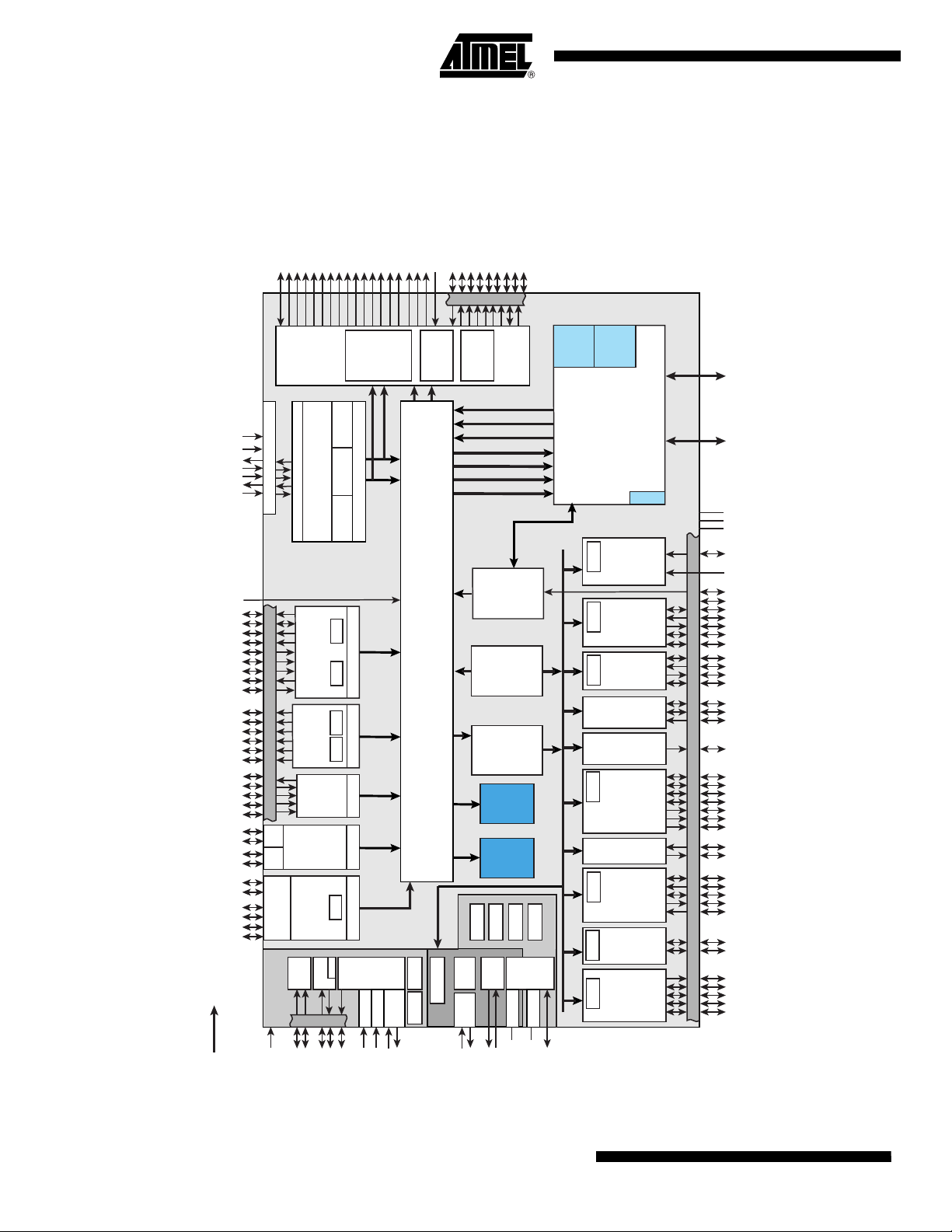
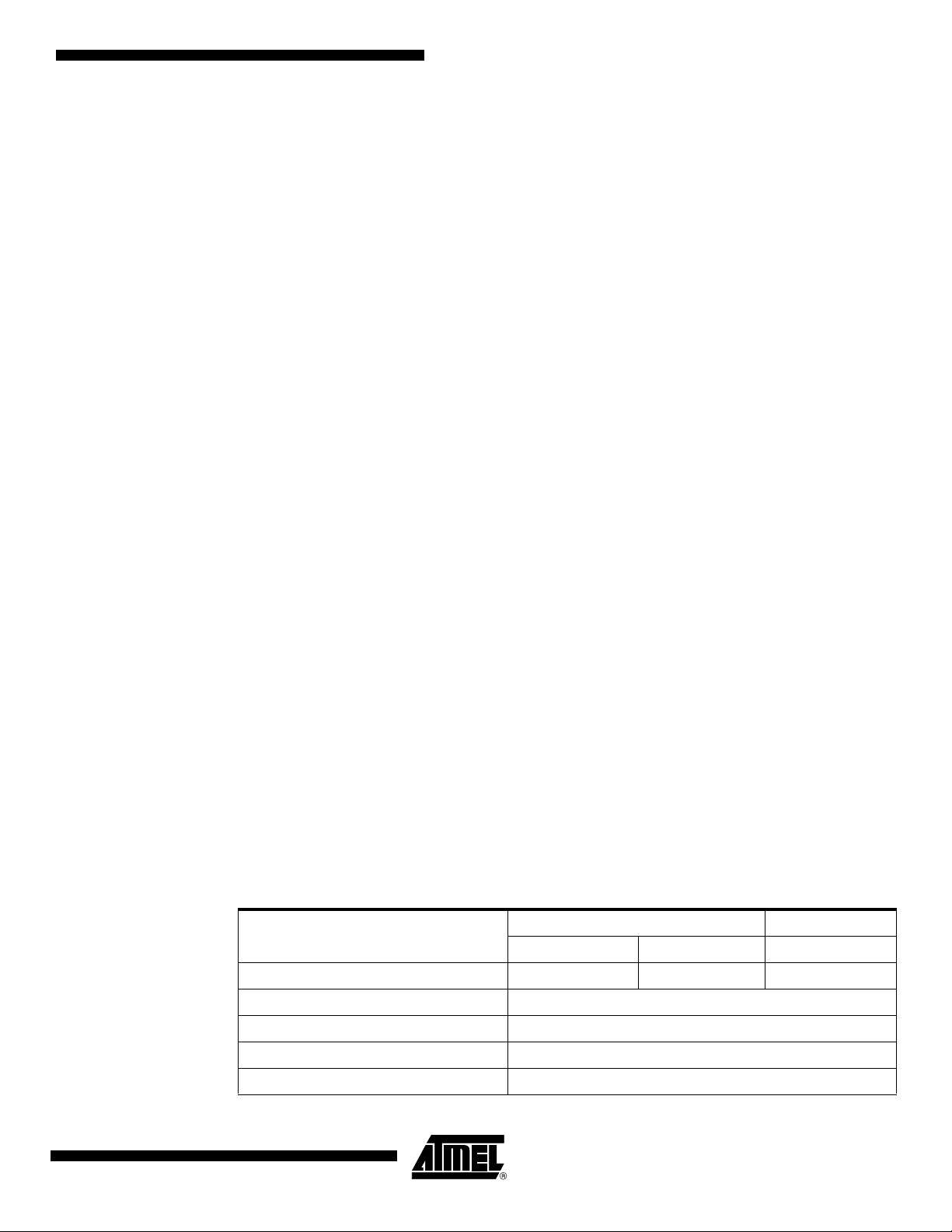
2. AT91CAP9S500A/AT91CAP9S250A Block Diagram
Figure 2-1. AT91CAP9S500A/AT91CAP9S250A Block Diagram
D0-D15
A0/NBS0
A2-A15, A18-A22
A16/BA0
A17/BA1
NCS0
NCS1/BCCS
NRD
NWR0/NWE
NWR1/NBS1
NWR3/NBS3
SDCK, SDCKN
RAS/BCADV, CAS/BCOE
DQS0, DQS1
DDRSDR
Controller
D
I
OSC
PLLB
SDWE/BCWE, SDA10
NANDOE, NANDWE
SDCKE/BCCRE
BCOWAIT
Memory
Burst Cellular
12-layer Matrix
PITWDT
4 GPREG
A23-A24
NWAIT
Static
Controller
RTT
OSC
NCS5/CFCS1
A25/CFRNW
NCS4/CFCS0
NCS2
NCS3/NANDCS
Memory
Controller
4-channel
Peripheral
23-channel
Bridge
Peripheral
SRAM
32Kbytes
ROM
32Kbytes
PIOA
PIOB
SHDC
D16-D31
CFCE1-CFCE2
DMA
DMA
PIOD
PIOC
RSTC
POR
POR
APB
10x
DPR
512x36
PDC
PDC
PDC
PDC
PDC
PDC
PDC
JTAGSEL
NTRST
RTCK
TCK
TMS
TDO
TDI
JTAG Boundary Scan
BMS
EF100
EMDIO
EMDC
ETX0-ETX3
ERX0-ERX3
ERXER-ERXDV
ECRS-ECOL
ETXEN-ETXER
ERXCK-ETXCK/EREFCK
LCDCC
LCDDEN
LCDDOTCK
LCDHSYNC
LCDVSYNC
LCDD0-LCDD23
ISI_MCK
ISI_VSYNC
ISI_HSYNC
ISI_DO-ISI_D11
ISI_PCK
HDMB
HDPB
HDMA
HDPA
FSDM
FSDP
HSDM
HSDP
PLLRC
VBG
SLAVEMASTER
System
Transc.
Transc.
UTMI+
Transc.
Controller
EBI
A1/NBS2/NWR2
& ECC
NAND Flash
CompactFlash
DCache
MMU
In-Circuit Emulator
ICache
ARM926EJ-S Processor
FIFO
MAC
FIFO
10/100 Ethernet
FIFO
LCD
Controller
LUT
Image
Sensor
Interface
USB
OHCI
FIFO
USB
Device
High-Speed
PDC
AIC
DBGU
16K bytes
Bus Interface
16K bytes
DMA
DMA
DMA
DMA
DMA
PMC
PLLA
8x
SPR
512x72
500K Gates (CAP9500)
250K Gates (CAP9250)
Metal Programable Block
L
L
D
ADC
10-bit
8-channel
SSC0
SSC1
AC97C
TC0
TC1
TC2
PWMC
SPI0
SPI1
CAN
USART0
USART1
USART2
TWI
MCI0
MCI1
TWD
CK
CDA
CDB
GNDANA
VDDANA
ADVREF
ADTRIG
AD0-AD7
RK0-RK1
RF0-RF1
RD0-RD1
TD0-TD1
TF0-TF1
TK0-TK1
AC97TX
AC97RX
AC97FS
AC97CK
MISO
MOSI
SPCK
NPCS0
NPCS1
NPCS2
NPCS3
CANRX
CANTX
TWCK
DA0-DA3
DB0-DB3
MPIOB0-MPIOB44
MPIOA0-MPIOA31
DMARQ0-DMARQ3
TIOB0-TIOB2
TIOA0-TIOA2
TCLK0-TCLK2
PWM0-PWM3
SPI0_, SPI1_
TXD0-TXD2
RDX0-RDX2
SCK0-SCK2
RTS0-RTS2
CTS0-CTS2
MCI0_, MCI_1
FIQ
TST
4
AT91CAP9S500A/AT91CAP9S250A
DTXD
DRXD
IRQ0-IRQ1
PCK0-PCK3
PLLRCB
PLLRCA
XIN
XOUT
XIN32
XOUT32
SHDN
WKUP
VDDBU
NRST
VDDCORE
6264A–CAP–21-May-07
Page 5

AT91CAP9S500A/AT91CAP9S250A
3. Signal Description
Table 3-1 gives details on the signal name classified by peripheral.
Table 3-1. Signal Description List
Active
Signal Name Function Type
Power Supplies
VDDIOM EBI I/O Lines Power Supply Power 1.65V to 3.6V
VDDIOP0 Peripherals I/O Lines Power Supply Power 3.0V to 3.6V
VDDIOP1 Peripherals I/O Lines Power Supply Power 1.65V to 3.6V
VDDIOMPA MP Block I/O A Lines Power Supply Power 1.65V to 3.6V
VDDIOMPB MP Block I/O B Lines Power Supply Power 1.65V to 3.6V
VDDBU Backup I/O Lines Power Supply Power 1.08V to 1.32V
VDDPLL PLL Power Supply Power 3.0V to 3.6V
VDDUTMII USB UTMI+ Interface Power Supply Power 3.0V to 3.6V
VDDUTMIC USB UTMI+ Core Power Supply Power 1.08V to 1.32V
VDDUPLL USB UTMI+ PLL Power Supply Power 1.08V to 1.32V
Level Comments
VDDANA ADC Analog Power Supply Power 3.0V to 3.6V
VDDCORE Core Chip Power Supply Power 1.08V to 1.32V
GND Ground Ground
GNDPLL PLL Ground Ground
GNDUTMII USB UTMI+ Interface Ground Ground
GNDUTMIC USB UTMI+ Core Ground Ground
GNDUPLL USB UTMI+ PLL Ground Ground
GNDANA ADC Analog Ground Ground
GNDBU Backup Ground Ground
GNDTHERMAL Thermal Ground Ball Ground
Clocks, Oscillators and PLLs
XIN Main Oscillator Input Input
XOUT Main Oscillator Output Output
XIN32 Slow Clock Oscillator Input Input
XOUT32 Slow Clock Oscillator Output Output
PLLRCA PLL A Filter Input
PLLRCB PLL B Filter Input
Thermally coupled with
package substrate
PCK0 - PCK3 Programmable Clock Output Output
Shutdown, Wakeup Logic
SHDN Shutdown Control Output Do not tie over VDDBU
WKUP Wake-Up Input Input
6264A–CAP–21-May-07
Accept between 0V and
VDDBU
5
Page 6

Table 3-1. Signal Description List (Continued)
Active
Signal Name Function Type
ICE and JTAG
NTRST Test Reset Signal Input Low No pull-up resistor
TCK Test Clock Input No pull-up resistor
TDI Test Data In Input No pull-up resistor
TDO Test Data Out Output
TMS Test Mode Select Input No pull-up resistor
JTAGSEL JTAG Selection Input Pull-down resistor
RTCK Return Test Clock Output
Reset/Test
NRST Microcontroller Reset I/O Low Pull-up resistor
TST Test Mode Select Input Pull-down resistor
BMS Boot Mode Select Input Pull-up resistor
Debug Unit - DBGU
DRXD Debug Receive Data Input
DTXD Debug Transmit Data Output
Level Comments
Advanced Interrupt Controller - AIC
IRQ0 - IRQ1 External Interrupt Inputs Input
FIQ Fast Interrupt Input Input
PIO Controller - PIOA - PIOB - PIOC - PIOD
PA0 - PA31 Parallel IO Controller A I/O Pulled-up input at reset
PB0 - PB31 Parallel IO Controller B I/O Pulled-up input at reset
PC0 - PC31 Parallel IO Controller C I/O Pulled-up input at reset
PD0 - PD31 Parallel IO Controller D I/O Pulled-up input at reset
Direct Memory Access Controller - DMA
DMARQ0-DMARQ3 DMA Requests Input
External Bus Interface - EBI
D0 - D31 Data Bus I/O Pulled-up input at reset
A0 - A25 Address Bus Output 0 at reset
NWAIT External Wait Signal Input Low
Static Memory Controller - SMC
NCS0 - NCS5 Chip Select Lines Output Low
NWR0 - NWR3 Write Signal Output Low
NRD Read Signal Output Low
NWE Write Enable Output Low
NBS0 - NBS3 Byte Mask Signal Output Low
6
AT91CAP9S500A/AT91CAP9S250A
6264A–CAP–21-May-07
Page 7

AT91CAP9S500A/AT91CAP9S250A
Table 3-1. Signal Description List (Continued)
Active
Signal Name Function Type
CompactFlash Support
CFCE1 - CFCE2 CompactFlash Chip Enable Output Low
CFOE CompactFlash Output Enable Output Low
CFWE CompactFlash Write Enable Output Low
CFIOR CompactFlash IO Read Output Low
CFIOW CompactFlash IO Write Output Low
CFRNW CompactFlash Read Not Write Output
CFCS0 - CFCS1 CompactFlash Chip Select Lines Output Low
NAND Flash Support
NANDCS NAND Flash Chip Select Output Low
NANDOE NAND Flash Output Enable Output Low
NANDWE NAND Flash Write Enable Output Low
DDR/SDRAM Controller
SDCK DDR/SDRAM Clock Output
SDCKN DDR Inverted Clock Output
Level Comments
DQS0 DDR Data Qualifier Strobe 0 I/O
DQS1 DDR Data Qualifier Strobe 1 I/O
SDCKE SDRAM Clock Enable Output High
SDCS SDRAM Controller Chip Select Output Low
BA0 - BA1 Bank Select Output
SDWE SDRAM Write Enable Output Low
RAS - CAS Row and Column Signal Output Low
SDA10 SDRAM Address 10 Line Output
Burst CellularRAM Controller
BCCK Burst CellularRAM Clock Output
BCCRE Burst CellularRAM Enable Output
BCADV Burst CellularRAM Burst Advance Signal Output
BCWE Burst CellularRAM Write Enable Output
BCOE Burst CellularRAM Output Enable Output
BCOWAIT Burst CellularRAM Output Wait Input
Multimedia Card Interface MCI
MCIx_CK Multimedia Card Clock Output
MCIx_CD Multimedia Card Command I/O
MCIx_D0 - D3 Multimedia Card Data I/O
Universal Synchronous Asynchronous Receiver Transmitter USART
6264A–CAP–21-May-07
7
Page 8

Table 3-1. Signal Description List (Continued)
Signal Name Function Type
SCKx USARTx Serial Clock I/O
TXDx USARTx Transmit Data I/O
RXDx USARTx Receive Data Input
RTSx USARTx Request To Send Output
CTSx USARTx Clear To Send Input
Synchronous Serial Controller - SSC
TDx SSCx Transmit Data Output
RDx SSCx Receive Data Input
TKx SSCx Transmit Clock I/O
RKx SSCx Receive Clock I/O
TFx SSCx Transmit Frame Sync I/O
RFx SSCx Receive Frame Sync I/O
AC97 Controller - AC97C
AC97RX AC97 Receive Signal Input
AC97TX AC97 Transmit Signal Output
Active
Level Comments
AC97FS AC97 Frame Synchronization Signal Output
AC97CK AC97 Clock signal Input
Timer/Counter - TC
TCLKx TC Channel x External Clock Input Input
TIOAx TC Channel x I/O Line A I/O
TIOBx TC Channel x I/O Line B I/O
Pulse Width Modulation Controller- PWMC
PMWx Pulse Width Modulation Output Output
Serial Peripheral Interface - SPI
SPIx_MISO Master In Slave Out I/O
SPIx_MOSI Master Out Slave In I/O
SPIx_SPCK SPI Serial Clock I/O
SPIx_NPCS0 SPI Peripheral Chip Select 0 I/O Low
SPIx_NPCS1 - SPIx_NPCS3 SPI Peripheral Chip Select Output Low
Two-Wire Interface
TWD Two-wire Serial Data I/O
TWCK Two-wire Serial Clock I/O
CAN Controller
CANRX CAN input Input
CANTX CAN output Output
8
AT91CAP9S500A/AT91CAP9S250A
6264A–CAP–21-May-07
Page 9

AT91CAP9S500A/AT91CAP9S250A
Table 3-1. Signal Description List (Continued)
Active
Signal Name Function Type
LCD Controller - LCDC
LCDD0 - LCDD23 LCD Data Bus Input
LCDVSYNC LCD Vertical Synchronization Output
LCDHSYNC LCD Horizontal Synchronization Output
LCDDOTCK LCD Dot Clock Output
LCDDEN LCD Data Enable Output
LCDCC LCD Contrast Control Output
Ethernet 10/100 E
ETXCK/EREFCK Transmit Clock or Reference Clock Input MII only, REFCK in RMII
ERXCK Receive Clock Input MII only
ETXEN Transmit Enable Output
ETX0-ETX3 Transmit Data Output ETX0-ETX1 only in RMII
ETXER Transmit Coding Error Output MII only
ERXDV Receive Data Valid Input
Level Comments
RXDV in MII, CRSDV in
RMII
ERX0-ERX3 Receive Data Input ERX0-ERX1 only in RMII
ERXER Receive Error Input
ECRS Carrier Sense and Data Valid Input MII only
ECOL Collision Detect Input MII only
EMDC Management Data Clock Output
EMDIO Management Data Input/Output I/O
EF100 Force 100Mbit/sec. Output High RMII only
USB High Speed Device
FSDM USB Full Speed Data - Analog
FSDP USB Full Speed Data + Analog
HSDM USB High Speed Data - Analog
HSDP USB High Speed Data + Analog
VBG Bias Voltage Reference Analog
PLLRCU USB PLL Test Pad Analog
OHCI USB Host Port
HDPA USB Host Port A Data + Analog
HDMA USB Host Port A Data - Analog
HDPB USB Host Port B Data + Analog
HDMB USB Host Port B Data - Analog
ADC
AD0-AD7 Analog Inputs Analog
6264A–CAP–21-May-07
9
Page 10
Table 3-1. Signal Description List (Continued)
Signal Name Function Type
ADVREF ADC Voltage Reference Analog
ADTRIG ADC Trigger Input
Image Sensor Interface - ISI
ISI_D0-ISI_D11 Image Sensor Data Input
ISI_MCK Image Sensor Reference Clock Output
ISI_HSYNC Image Sensor Horizontal Synchro Input
ISI_VSYNC Image Sensor Vertical Synchro Input
ISI_PCK Image Sensor Data Clock Input
MPBLOCK - MPB
MPIOA0-MPIOA31 MPBlock I/Os A I/O
MPIOB0-MPIOB44 MPBlock I/Os B I/O
4. Package and Pinout
The AT91CAP9S500A/AT91CAP9S250A is available in a 400-ball RoHS-compliant BGA package, 17 x 17 mm, 0.8mm ball pitch.
Active
Level Comments
4.1 400-ball BGA Package Outline
Figure 4-1 shows the orientation of the 400-ball BGA Package.
A detailed mechanical description is given in the section “AT91CAP9S500A/AT91CAP9S250A
Mechanical Characteristics” of the product datasheet.
Figure 4-1. 400-ball BGA Package Outline (Top View)
20
19
18
17
16
15
14
13
12
11
10
9
8
7
6
5
4
3
2
1
ABCDE FGHJ KL MNPRT UV
BALL A1
YW
10
AT91CAP9S500A/AT91CAP9S250A
6264A–CAP–21-May-07
Page 11

AT91CAP9S500A/AT91CAP9S250A
4.2 400-ball BGA Package Pinout
Table 4-1. AT91CAP9S500A/AT91CAP9S250A Pinout for 400-ball BGA Package
Pin Signal Name Pin Signal Name Pin Signal Name Pin Signal Name
A1 PC5 F1 PA3 L1 PA22 T1 PD22
A2 PC3 F2 PA4 L2 PA25 T2 PD23
A3 PC2 F3 PA8 L3 PA29 T3 PD30
A4 PC1 F4 PA5 L4 PA31 T4 VDDCORE
A5 PC0 F5 PA6 L5 PD6 T5 SDDRCS
A6 BMS F6 VDDIOM L6 GNDIO T6 DQS0
A7 NRST F7 VDDIOP0 L7 GNDCORE T7 D4
A8 GNDCORE F8 PC24 L8 PA18 T8 D11
A9 PB18 F9 NC L9 GNDTHERMAL T9 D14
A10 PB17 F10 VDDCORE L10 GNDTHERMAL T10 SDA10
A11 PB14 F11 GNDIO L11 GNDTHERMAL T11 VDDCORE
A12 PB15 F12 PB23 L12 GNDTHERMAL T12 MPIOA0
A13 GNDANA F13 PB6 L13 GNDCORE T13 MPIOA9
A14 PB26 F14 NC L14 GNDIO T14 GNDIO
A15 VDDIOP0 F15 NC L15 VDDCORE T15 MPIOA25
A16 GNDIO F16 NC L16 MPIOB28 T16 MPIOA24
A17 FSDP F17 GNDPLL L17 MPIOB32 T17 MPIOA29
A18 FSDM F18 WKUP0 L18 MPIOB34 T18 MPIOB3
A19 HSDP F19 SHDW L19 MPIOB31 T19 MPIOB17
A20 HSDM F20 PLLRCA L20 MPIOB29 T20 MPIOB18
B1 PC17 G1 PA7 M1 PA26 U1 PD25
B2 PC16 G2 PA10 M2 PA30 U2 PD31
B3 PC14 G3 PA11 M3 PD11 U3 BCCLK
B4 PC11 G4 PA9 M4 PD12 U4 A0
B5 PC10 G5 PA12 M5 PD13 U5 D0
B6 PC9 G6 PD10 M6 PD15 U6 D1
B7 TDO G7 GNDIO M7 GNDCORE U7 NWR1
B8 TCK G8 GNDCORE M8 PA28 U8 DQS1
B9 PB20 G9 VDDIOP0 M9 GNDTHERMAL U9 A7
B10 PB19 G10 PC8 M10 GNDTHERMAL U10 A13
B11 PB13 G11 PB25 M11 GNDTHERMAL U11 A20
B12 ADVREF G12 PB21 M12 GNDTHERMAL U12 GNDIO
B13 PB16 G13 PB8 M13 NRD U13 MPIOA4
B14 PB27 G14 PB0 M14 MPIOB26 U14 MPIOA11
B15 PB24 G15 PB2 M15 GNDIO U15 MPIOA16
B16 HDMA G16 NC M16 MPIOB16 U16 VDDMPIOA
B17 VDDIOP0 G17 VDDPLL M17 GNDCORE U17 MPIOA23
6264A–CAP–21-May-07
11
Page 12

Table 4-1. AT91CAP9S500A/AT91CAP9S250A Pinout for 400-ball BGA Package (Continued)
Pin Signal Name Pin Signal Name Pin Signal Name Pin Signal Name
B18 GNDIO G18 GNDCORE M18 MPIOB27 U18 MPIOA28
B19 VDDUTMII G19 TST M19 MPIOB25 U19 MPIOB6
B20 GNDUTMII G20 PLLRCB M20 MPIOB24 U20 MPIOB9
C1 PC23 H1 PA13 N1 PD7 V1 PD26
C2 PC22 H2 PA14 N2 PD8 V2 RAS
C3 PC21 H3 PD0 N3 PD16 V3 SDCKE
C4 PC20 H4 PA15 N4 PD19 V4 D3
C5 PC18 H5 PD1 N5 PD20 V5 VDDIOM
C6 PC15 H6 VDDIOP1 N6 PD29 V6 D5
C7 PC12 H7 VDDCORE N7 GNDIO V7 D9
C8 PC6 H8 GNDIO N8 VDDIOM V8 D15
C9 NTRST H9 GNDIO N9 NCS1 V9 A11
C10 TDI H10 PB10 N10 VDDCORE V10 GNDCORE
C11 VDDANA H11 PB4 N11 A3 V11 A22
C12 PB12 H12 VDDMPIOB N12 A6 V12 MPIOA1
C13 PB29 H13 JTAGSEL N13 VDDCORE V13 MPIOA6
C14 PB9 H14 GNDCORE N14 MPIOB11 V14 MPIOA10
C15 PB7 H15 GNDPLL N15 MPIOB13 V15 MPIOA13
C16 HDPA H16 NC N16 MPIOB12 V16 MPIOA17
C17 HDPB H17 VDDCORE N17 MPIOB14 V17 MPIOA20
C18 VDDUPLL H18 MPIOB44 N18 MPIOB15 V18 MPIOA27
C19 VDDUTMIC H19 XOUT32 N19 MPIOB22 V19 MPIOB5
C20 VBG H20 XIN32 N20 MPIOB23 V20 VDDMPIOB
D1 PC29 J1 PD3 P1 PD9 W1 SDWE
D2 PC28 J2 PD2 P2 PD14 W2 OWAIT
D3 PC27 J3 PD5 P3 PD18 W3 NANDWE
D4 PC26 J4 PA17 P4 PD27 W4 GNDIO
D5 PC25 J5 PA19 P5 PD28 W5 D6
D6 PC19 J6 VDDIOP0 P6 VDDIOM W6 A2
D7 NANDOE J7 PA16 P7 NWR3 W7 A5
D8 PC7 J8 GNDCORE P8 D8 W8 A14
D9 GNDIO J9 GNDTHERMAL P9 D10 W9 A17
D10 TMS J10 GNDTHERMAL P10 GNDIO W10 A19
D11 NC J11 GNDTHERMAL P11 A9 W11 NWR0
D12 PB31 J12 GNDTHERMAL P12 A12 W12 MPIOA2
D13 PB22 J13 GNDIO P13 NC W13 MPIOA5
D14 VDDCORE J14 GNDBU P14 MPIOB8 W14 MPIOA8
D15 PB3 J15 GNDBU P15 MPIOB0 W15 MPIOA12
12
AT91CAP9S500A/AT91CAP9S250A
6264A–CAP–21-May-07
Page 13

AT91CAP9S500A/AT91CAP9S250A
Table 4-1. AT91CAP9S500A/AT91CAP9S250A Pinout for 400-ball BGA Package (Continued)
Pin Signal Name Pin Signal Name Pin Signal Name Pin Signal Name
D16 PB1 J16 MPIOB42 P16 MPIOB1 W16 MPIOA15
D17 HDMB J17 MPIOB39 P17 MPIOB7 W17 MPIOA21
D18 PLLRCU J18 MPIOB43 P18 MPIOB10 W18 MPIOA22
D19 GNDUTMIC J19 MPIOB41 P19 MPIOB21 W19 GNDIO
D20 GNDUPLL J20 GNDIO P20 VDDMPIOB W20 VDDCORE
E1 PC30 K1 PD4 R1 PD21 Y1 SDCK
E2 PA2 K2 PA21 R2 PD17 Y2 SDCKN
E3 PA1 K3 PA24 R3 PD24 Y3 A1
E4 PA0 K4 PA27 R4 CAS Y4 GNDCORE
E5 PC31 K5 PA23 R5 VDDCORE Y5 A4
E6GNDIOK6GNDIOR6D2 Y6A8
E7 VDDCORE K7 PA20 R7 D7 Y7 A10
E8 PC13 K8 VDDCORE R8 VDDIOM Y8 A15
E9 PC4 K9 GNDTHERMAL R9 D13 Y9 A18
E10 RTCK K10 GNDTHERMAL R10 D12 Y10 A21
E11 VDDIOP0 K11 GNDTHERMAL R11 VDDIOM Y11 NCS0
E12 PB30 K12 GNDTHERMAL R12 A16 Y12 MPIOA3
E13 PB28 K13 GNDCORE R13 VDDIOM Y13 MPIOA7
E14 PB11 K14 MPIOB33 R14 NC Y14 VDDMPIOA
E15 PB5 K15 MPIOB30 R15 NC Y15 MPIOA14
E16 NC K16 MPIOB35 R16 NC Y16 MPIOA18
E17 VDDPLL K17 MPIOB38 R17 MPIOB2 Y17 MPIOA19
E18 VDDBU K18 MPIOB40 R18 MPIOB4 Y18 MPIOA26
E19 XIN K19 MPIOB37 R19 MPIOB19 Y19 MPIOA30
E20 XOUT K20 MPIOB36 R20 MPIOB20 Y20 MPIOA31
5. Power Considerations
5.1 Power Supplies
The AT91CAP9S500A/AT91CAP9S250A has several types of power supply pins:
• VDDCORE pins: Power the core, including the processor, the embedded memories and the
peripherals; voltage range between1.08V and 1.32V, 1.2V nominal.
• VDDIOM pins: Power the External Bus Interface; voltage ranges between 1.65V and 1.95V
(1.8V nominal) or between 3.0V and 3.6V (3.3V nominal).
• VDDIOP0 pins: Power the Peripherals I/O lines and the USB transceivers; voltage range
between 3.0V and 3.6V, 3.3V nominal.
• VDDIOP1 pins: Power the Peripherals I/O lines involving the Image Sensor Interface; voltage
ranges from 1.65V to 3.6V, 1.8V, 2.5V, 3V or 3.3V nominal.
6264A–CAP–21-May-07
13
Page 14

• VDDIOMPA pins: Power the MP Block I/O A lines; voltage ranges from 1.65V to 3.6V, 1.8V,
2.5V, 3V or 3.3V nominal.
• VDDIOMPB pins: Power the dedicated MP Block I/O B lines; voltage ranges from 1.65V to
3.6V, 1.8V, 2.5V, 3V or 3.3V nominal.
• VDDBU pin: Powers the Slow Clock oscillator and a part of the System Controller; voltage
range between1.08V and 1.32V, 1.2V nominal.
• VDDPLL pin: Powers the PLL cells; voltage ranges between 3.0V to 3.6V, 3.3V nominal.
• VDDUTMII pin: Powers the UTMI+ interface; voltage ranges from 3.0V to 3.6V, 3.3V nominal.
• VDDUTMIC pin: Powers the UTMI+ core; voltage ranges between 1.08V and 1.32V, 1.2V
nominal.
• VDDUPLL pin: Powers the USB PLL cell; voltage ranges between 1.08V and 1.32V, 1.2V
nominal.
• VDDANA pin: Powers the ADC cell; voltage ranges between 3.0V and 3.6V, 3.3V nominal.
The power supplies VDDIOM, VDDIOP0 and VDDIOP1 are identified in the pinout table and the
multiplexing tables. These supplies enable the user to power the device differently for interfacing
with memories and for interfacing with peripherals.
Ground pins GNDIO are common to VDDIOM, VDDIOP0, VDDIOP1, VDDIOMPA and VDDIOMPB pin power supplies. Separated ground pins are provided for VDDCORE, VDDBU,
VDDPLL, VDDUTMII, VDDUTMIC, VDDUPLL and VDDANA. These ground pins are, respectively, GNDBU, GNDOSC, GNDPLL, GNDUTMII, GNDUTMIC, GNDUPLL and GNDANA.
Special GNDTHERMAL ground balls are thermally coupled with package substrate.
5.2 Power Consumption
The AT91CAP9S500A/AT91CAP9S250A consumes about 700 µA (TBC) of static current on
VDDCORE at 25°C. This static current may go up to 7 mA (TBC) if the temperature increases to
85°C.
On VDDBU, the current does not exceed 3 µA(TBC) @25°C, but can rise at up to 20 µA(TBC)
@85°C.
For dynamic power consumption, the AT91CAP9S500A/AT91CAP9S250A consumes a maximum of 90 mA (TBC) on VDDCORE at typical conditions (1.2V, 25°C, processor running fullperformance algorithm).
5.3 Programmable I/O Lines Power Supplies
The power supply pins VDDIOM, VDDMPIOA and VDDMPIOB accept two voltage ranges. This
allows the device to reach its maximum speed either out of 1.8V or 3.3V external memories.
The target maximum speed is 100 MHz on the pin DDR/SDR and MPIOA or MPIOB pins loaded
with 30 pF for power supply at 1.8V and 50 pF for power supply at 3.3V. The other signals (control, address and data signals) do not go over 50 MHz.
The voltage ranges are determined by programming registers in the Chip Configuration registers
located in the Matrix User Interface.
14
At reset, the selected voltage defaults to 3.3V nominal and power supply pins can accept either
1.8V or 3.3V. Obviously, the device cannot reach its maximum speed if the voltage supplied to
the pins is 1.8V only. The user must make sure to program the EBI voltage range before getting
the device out of its Slow Clock Mode.
AT91CAP9S500A/AT91CAP9S250A
6264A–CAP–21-May-07
Page 15

6. I/O Line Considerations
6.1 JTAG Port Pins
TMS, TDI and TCK are Schmitt trigger inputs and have no pull-up resistors.
TDO and RTCK are outputs, driven at up to VDDIOP0, and have no pull-up resistors.
The JTAGSEL pin is used to select the JTAG boundary scan when asserted at a high level. It
integrates a permanent pull-down resistor of about 15 kΩ to GNDBU so that it can be left uncon-
nected for normal operations.
The NTRST signal is described in Section 6.3 ”Reset Pins” on page 15.
All the JTAG signals are supplied with VDDIOP0.
6.2 Test Pin
The TST pin is used for manufacturing test purposes when asserted high. It integrates a permanent pull-down resistor of about 15 kΩ to GNDBU so that it can be left unconnected for normal
operations. Driving this line at a high level leads to unpredictable results.
This pin is supplied with VDDBU.
AT91CAP9S500A/AT91CAP9S250A
6.3 Reset Pins
NRST is an open-drain output integrating a non-programmable pull-up resistor. It can be driven
with voltage at up to VDDIOP0.
NTRST is an input which allows reset of the JTAG Test Access port. It has no action on the
processor.
As the product integrates power-on reset cells that manage the processor and the JTAG reset,
the NRST and NTRST pins can be left unconnected.
The NRST and NTRST pins both integrate a permanent pull-up resistor of 90 kΩ minimum to
VDDIOP0.
The NRST signal is inserted in the Boundary Scan.
6.4 PIO Controllers
All the I/O lines which are managed by the PIO Controllers integrate a programmable pull-up
resistor of 90 kΩ minimum. Programming of this pull-up resistor is performed independently for
each I/O line through the PIO Controllers.
After reset, all the I/O lines default as inputs with pull-up resistors enabled, except those multiplexed with the External Bus Interface signals that must be enabled as Peripheral at reset. This
is indicated in the column “Reset State” of the PIO Controller multiplexing tables.
6.5 Shutdown Logic Pins
The SHDN pin is an output only, which is driven by the Shutdown Controller only at low level. It
can be tied high with an external pull-up resistor at VDDBU only.
6264A–CAP–21-May-07
The pin WKUP is an input-only. It can accept voltages only between 0V and VDDBU.
15
Page 16

7. Processor and Architecture
7.1 ARM926EJ-S Processor
• RISC Processor based on ARM v5TEJ Architecture with Jazelle technology for Java
acceleration
• Two Instruction Sets
– ARM High-performance 32-bit Instruction Set
– Thumb High Code Density 16-bit Instruction Set
• DSP Instruction Extensions
• 5-Stage Pipeline Architecture:
– Instruction Fetch (F)
– Instruction
– Execute (E)
– Data Memory (M)
– Register Write (W)
• 16-Kbyte Data Cache, 16-Kbyte Instruction Cache
– Virtually-addressed 4-way Associative Cache
– Eight words per line
– Write-through and Write-back Operation
– Pseudo-random or Round-robin Replacement
• Write Buffer
– Main Write Buffer with 16-word Data Buffer and 4-address Buffer
– DCache Write-back Buffer with 8-word Entries and a Single Address Entry
– Software Control Drain
• Standard ARM v4 and v5 Memory Management Unit (MMU)
– Access Permission for Sections
– Access Permission for large pages and small pages can be specified separately for
each quarter of the page
– 16 embedded domains
• Bus Interface Unit (BIU)
– Arbitrates and Schedules AHB Requests
– Separate Masters for both instruction and data access providing complete Matrix
system flexibility
– Separate Address and Data Buses for both the 32-bit instruction interface and the
32-bit data interface
– On Address and Data Buses, data can be 8-bit (Bytes), 16-bit (Half-words) or 32-bit
(Words)
Decode (D)
7.2 Bus Matrix
16
AT91CAP9S500A/AT91CAP9S250A
• 12-layer Matrix, handling requests from 12 masters
• Programmable Arbitration strategy
– Fixed-priority Arbitration
6264A–CAP–21-May-07
Page 17

7.3 Matrix Masters
AT91CAP9S500A/AT91CAP9S250A
– Round-Robin Arbitration, either with no default master, last accessed default master
or fixed default master
• Burst Management
– Breaking with Slot Cycle Limit Support
– Undefined Burst Length Support
• One Address Decoder provided per Master
– Three different slaves may be assigned to each decoded memory area: one for
internal boot, one for external boot, one after remap
• Boot Mode Select
– Non-volatile Boot Memory can be internal or external
– Selection is made by BMS pin sampled at reset
• Remap Command
– Allows Remapping of an Internal SRAM in Place of the Boot Non-Volatile Memory
– Allows Handling of Dynamic Exception Vectors
The Bus Matrix of the AT91CAP9S500A/AT91CAP9S250A manages twelve Masters and thus
each master can perform an access concurrently with the others, assuming that the slave it
accesses is available.
7.4 Matrix Slaves
Each Master has its own decoder, which is defined specifically for each master. In order to simplify the addressing, all the masters have the same decoding.
Table 7-1. List of Bus Matrix Masters
Master 0 ARM926™ Instruction
Master 1 ARM926 Data
Master 2 Peripheral DMA Controller
Master 3 LCD Controller
Master 4 USB High Speed Device Controller
Master 5 Image Sensor Interface
Master 6 DMA Controller
Master 7 Ethernet MAC
Master 8 OHCI USB Host Controller
Master 9 MP Block Master 0
Master 10 MP Block Master 1
Master 11 MP Block Master 2
The Bus Matrix of the AT91CAP9S500A/AT91CAP9S250A manages ten Slaves. Each Slave
has its own arbiter, thus permitting a different arbitration per Slave to be programmed.
6264A–CAP–21-May-07
17
Page 18
The LCD Controller, the DMA Controller, the USB Host and the USB OTG have a user interface
mapped as a Slave of the Matrix. They share the same layer, as programming them does not
require a high bandwidth.
Table 7-2. List of Bus Matrix Slaves
Slave 0 Internal SRAM 32 Kbytes
Slave 1 MP Block Slave 0 (MP Block Internal Memories)
Internal ROM
LCD Controller User Interface
Slave 2
Slave 3 MP Block Slave 1 (MP Block Internal Memories)
Slave 4 External Bus Interface
Slave 5 DDR Controller Port 2
Slave 6 DDR Controller Port 3
Slave 7 MP Block Slave 2 (MP Block External Chip Selects)
Slave 8 MP Block Slave 3 (MP Block Internal Peripherals)
Slave 9 Internal Peripherals for AT91CAP9
DMA Controller User Interface
USB High Speed Device Interface
OHCI USB Host Interface
7.5 Master-to-Slave Access
All the Masters can normally access all the Slaves. However, some paths do not make sense,
such as allowing access from the Ethernet MAC to the Internal Peripherals. Thus, these paths
are forbidden or simply not wired, and shown “-” in Table 7-3,
“AT91CAP9S500A/AT91CAP9S250A Masters to Slaves Access,” on page 19.
18
AT91CAP9S500A/AT91CAP9S250A
6264A–CAP–21-May-07
Page 19

AT91CAP9S500A/AT91CAP9S250A
Table 7-3. AT91CAP9S500A/AT91CAP9S250A Masters to Slaves Access
Master 0 1 2 3 4 5 6 7 8 9 10 11
Slave
ARM926 Instruction
LCDCtrl
ARM926 Data
Peripheral DMA Ctrl
Device Ctrl
USB High Speed
Image Sensor Interface
DMA Ctrl
Ethernet MAC
OHCI USB Host Ctrl
MP Block Master 0
MP Block Master 1
MP Block Master 2
Internal SRAM
0
32 Kbytes
MP Block
1
Slave 0
XXXX X XXXXXXX
XXXX X XXXXXXX
Internal ROM X X X X X X X X X X X X
LCD
Controller
XX-- - ----XXX
User Interface
2
USB High
Speed Device
XX - - - - X - - X X X
Interface
OHCI USB
Host Interface
MPBlock
3
Slave 1
External Bus
4
Interface
XX-- - ----XXX
XXXX X XXXXXXX
XXXX X XXXXXXX
-
- DDR Port 0 X - - - - - - - - - - -
5 DDR Port 1 - X - - - - - - - - - -
6 DDR Port 2 X
DDR Port 3 X
7
8
9
MPBlock
Slave 2
MPBlock
Slave 3
Internal
Peripherals
XXXX X XXXXXXX
XXXX X XXXXXXX
XX X - - - X - - X X X
(1)
(1)
(1)
X
(1)
X
(1)
X
(1)
X
(1)
X
(1)
X
(1)
X
(1)
X
(1)
X
(1)
X
(1)
X
(1)
X
(1)
X
(1)
X
(1)
X
(1)
X
(1)
X
(1)
X
Note: 1. DDR Port 2 or Port 3 is selectable for each master through the Matrix Remap Control Register.
6264A–CAP–21-May-07
19
Page 20

7.6 Peripheral DMA Controller
• Acting as one Matrix Master
• Allows data transfers from/to peripheral to/from any memory space without any intervention
of the processor.
• Next Pointer Support, forbids strong real-time constraints on buffer management.
• Twenty-two Channels
– Two for each USART
– Two for the Debug Unit
– One for the TWI
– One for the ADC Controller
– Two for the AC97 Controller
– Two for each Serial Synchronous Controller
– Two for each Serial Peripheral Interface
– One for the each Multimedia Card Interface
The Peripheral DMA Controller handles transfer requests from the channel according to the following priorities (Low to High priorities):
– DBGU Transmit Channel
– USART2 Transmit Channel
– USART1 Transmit Channel
– USART0 Transmit Channel
– AC97 Transmit Channel
– SPI1 Transmit Channel
– SPI0 Transmit Channel
– SSC1 Transmit Channel
– SSC0 Transmit Channel
– DBGU Receive Channel
– TWI Transmit/Receive Channel
– ADC Receive Channel
– USART2 Receive Channel
– USART1 Receive Channel
– USART0 Receive Channel
– AC97 Receive Channel
– SPI1 Receive Channel
– SPI0 Receive Channel
– SSC1 Receive Channel
– SSC0 Receive Channel
– MCI1 Transmit/Receive Channel
– MCI0 Transmit/Receive Channel
7.7 DMA Controller
20
AT91CAP9S500A/AT91CAP9S250A
• Acting as one Matrix Master
6264A–CAP–21-May-07
Page 21

AT91CAP9S500A/AT91CAP9S250A
• Embeds 4 unidirectional channels with programmable priority
• Address Generation
– Source / destination address programming
– Address increment, decrement or no change
– DMA chaining support for multiple non-contiguous data blocks through use of linked
lists
– Scatter support for placing fields into a system memory area from a contiguous
transfer. Writing a stream of data into non-contiguous fields in system memory
– Gather support for extracting fields from a system memory area into a contiguous
transfer
– User enabled auto-reloading of source, destination and control registers from initially
programmed values at the end of a block transfer
– Auto-loading of source, destination and control registers from system memory at end
of block transfer in block chaining mode
– Unaligned system address to data transfer width supported in hardware
• Channel Buffering
– 8-word FIFO
– Automatic packing/unpacking of data to fit FIFO width
• Channel Control
– Programmable multiple transaction size for each channel
– Support for cleanly disabling a channel without data loss
– Suspend DMA operation
– Programmable DMA lock transfer support
• Transfer Initiation
– Support four External DMA Requests and four Internal DMA request from the MP
Block
– Support for Software handshaking interface. Memory mapped registers can be used
to control the flow of a DMA transfer in place of a hardware handshaking interface
• Interrupt
– Programmable Interrupt generation on DMA Transfer completion Block Transfer
completion, Single/Multiple transaction completion or Error condition
7.8 Debug and Test Features
• ARM926 Real-time In-circuit Emulator
– Two real-time Watchpoint Units
– Two Independent Registers: Debug Control Register and Debug Status Register
– Test Access Port Accessible through JTAG Protocol
– Debug Communications Channel
• Debug Unit
–Two-pin UART
– Debug Communication Channel Interrupt Handling
– Chip ID Register
• IEEE1149.1 JTAG Boundary-scan on All Digital Pins
6264A–CAP–21-May-07
21
Page 22
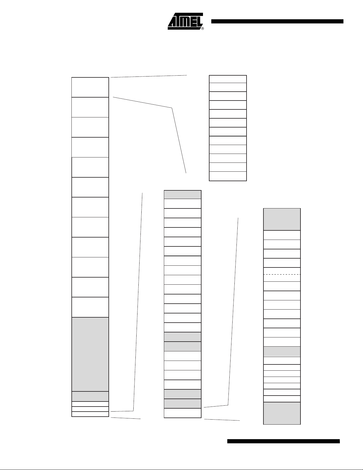
8. Memories
Figure 8-1. AT91CAP9S500A/AT91CAP9S250A Memory Mapping
0x0000 0000
0x0FFF FFFF
0x1000 0000
0x1FFF FFFF
0x2000 0000
0x2FFF FFFF
0x3000 0000
0x3FFF FFFF
0x4000 0000
0x4FFF FFFF
0x5000 0000
0x5FFF FFFF
0x6000 0000
0x6FFF FFFF
0x7000 0000
0x7FFF FFFF
0x8000 0000
0x8FFF FFFF
0x9000 0000
0x9FFF FFFF
0xA000 0000
0xAFFF FFFF
0xB000 0000
0xBFFF FFFF
0xC000 0000
0xEFFF FFFF
0xF000 0000
0xFCFF FFFF
0xFD00 0000
0xFE00 0000
0xFF00 0000
0xFFFF FFFF
Address Memory Space
Internal Memories
EBI
Chip Select 0
EBI
Chip Select 1/
EBI BCRAMC
EBI
Chip Select 2
EBI
Chip Select 3/
NANDFlash
EBI
Chip Select 4/
Compact Flash
Slot 0
EBI
Chip Select 5/
Compact Flash
Slot 1
EBI
DDRSDRC
MPB SLAVE2
Chip Select 0
MPB SLAVE 2
Chip Select 1
MPB SLAVE 2
Chip Select 2
MPB SLAVE 2
Chip Select 3
Undefined
(Abort)
Undefined
(Abort)
MPB SLAVE3
MPB SLAVE3
Internal Peripherals
256M Bytes
256M Bytes
256M Bytes
256M Bytes
256M Bytes
256M Bytes
256M Bytes
256M Bytes
256M Bytes
256M Bytes
256M Bytes
256M Bytes
768M Bytes
208M Bytes
16M Bytes
16M Bytes
16M Bytes
0xFF00 0000
0xFFF7 8000
0xFFF7 C000
0xFFF8 0000
0xFFF8 4000
0xFFF8 8000
0xFFF8 C000
0xFFF9 0000
0xFFF9 4000
0xFFF9 8000
0xFFF9 C000
0xFFFA 0000
0xFFFA 4000
0xFFFA 8000
0xFFFA C000
0xFFFB 0000
0xFFFB 4000
0xFFFB 8000
0xFFFB C000
0xFFFC 0000
0xFFFC 4000
0xFFFC 8000
0xFFFC C000
0xFFFF C000
0xFFFF FFFF
Peripheral Mapping
TCO, TC1, TC2
0x0000 0000
0x0010 0000
0x0020 0000
0x0030 0000
0x0040 0000
0x0050 0000
0x0060 0000
0x0070 0000
0x0080 0000
0x0090 0000
0x00A0 0000
0x00B0 0000
Reserved
UDPHS
MCI0
MCI1
TWI
USART0
USART1
USART2
SSC0
SSC1
AC97C
SPI0
SPI1
CAN0
Reserved
Reserved
PWMC
EMAC
ADCC
ISI
Reserved
Reserved
SYSC
Internal Memory Mapping
Boot Memory (1)
SRAM
MPB SLAVE0
MPB SLAVE0
ROM
LCDC
UDPHS
USB HOST
MPB SLAVE1
MPB SLAVE1
MPB SLAVE1
MPB SLAVE1
16K Bytes
16K Bytes
16K Bytes
16K Bytes
16K Bytes
16K Bytes
16K Bytes
16K Bytes
16K Bytes
16K Bytes
16K Bytes
16K Bytes
16K Bytes
16K Bytes
16K Bytes
16K Bytes
16K Bytes
16K Bytes
16K Bytes
16K Bytes
16K Bytes
16K Bytes
16K Bytes
16K Bytes
0xFFFF C000
0xFFFF E200
0xFFFF E400
0xFFFF E600
0xFFFF E800
0xFFFF EA00
0xFFFF EB10
0xFFFF EC00
0xFFFF EE00
0xFFFF F000
0xFFFF F200
0xFFFF F400
0xFFFF F600
0xFFFF F800
0xFFFF FA00
0xFFFF FC00
0xFFFF FD00
0xFFFF FD10
0xFFFF FD20
0xFFFF FD30
0xFFFF FD40
0xFFFF FD50
0xFFFF FD60
0xFFFF FFFF
Notes :
(1) Can be ROM, EBI_NCS0 or SRAM
depending on BMS and REMAP
System Controller Mapping
Reserved
ECC
BCRAMC
DDRSDRC
SMC
MATRIX
CCFG
DMA
DBGU
AIC
PIOA
PIOB
PIOC
PIOD
Reserved
PMC
RSTC
SHDC
RTT
PIT
WDT
GPBR
Reserved
512 Bytes
512 Bytes
512 bytes
512 Bytes
512 Bytes
512 Bytes
512 Bytes
512 bytes
512 bytes
512 Bytes
512 bytes
512 bytes
512 bytes
256 Bytes
16 Bytes
16 Bytes
16 Bytes
16 Bytes
16 Bytes
16 Bytes
22
AT91CAP9S500A/AT91CAP9S250A
6264A–CAP–21-May-07
Page 23
AT91CAP9S500A/AT91CAP9S250A
A first level of address decoding is performed by the Bus Matrix, i.e., the implementation of the
Advanced High-performance Bus (AHB) for its Master and Slave interfaces with additional
features.
Decoding breaks up the 4G bytes of address space into 16 banks of 256M bytes. The banks 1 to
7 are directed to the EBI that associates these banks to the external chip selects EBI_NCS0 to
EBI_NCS5 and EBI_SDDRCS. The bank 0 is reserved for the addressing of the internal memories, and a second level of decoding provides 1M byte of internal memory area. The banks 8 to
11 are directed to MP Block (Slave 2) and may be used to address external memories. The bank
15 is split into three parts, one reserved for the peripherals that provides access to the Advanced
Peripheral Bus (APB), the two others are directed to MP Block (Slave 3) and may provide
access to the MP Block APB or to other AHB peripherals.
Other areas are unused and performing an access within them provides an abort to the master
requesting such an access.
Each Master has its own bus and its own decoder, thus allowing a different memory mapping
per Master. However, in order to simplify the mappings, all the masters have a similar address
decoding.
Regarding Master 0 and Master 1 (ARM926 Instruction and Data), three different Slaves are
assigned to the memory space decoded at address 0x0: one for internal boot, one for external
boot and one after remap. Refer to Table 8-1, “Internal Memory Mapping,” on page 23 for
details.
8.1 Embedded Memories
• 32 Kbyte ROM
– Single Cycle Access at full matrix speed
• 32 Kbyte Fast SRAM
– Single Cycle Access at full matrix speed
• 20 Kbyte MP Block Fast Dual Port RAM (ten 512x36 DPR instances)
– Used as Dual Port RAM completely managed by MP Block
• 32 Kbyte MP Block Fast Single Port RAM (eight 512x72 SPR instances)
– Used as Single Port RAM completely managed by MP Block
8.1.1 Internal Memory Mapping
Table 8-1 summarizes the Internal Memory Mapping, depending on the Remap status and the
BMS state at reset.
Table 8-1. Internal Memory Mapping
0x0000 0000 ROM EBI_NCS0 SRAM
0x0010 0000 SRAM
0x0020 0000 MP Block Slave 0 (hsel[0])
0x0030 0000 MP Block Slave 0 (hsel[1])
0x0040 0000 ROM
Address
REMAP = 0 REMAP = 1
BMS = 0 BMS = 1
6264A–CAP–21-May-07
23
Page 24

Table 8-1. Internal Memory Mapping (Continued)
0x0050 0000 LCD Controller User Interface
0x0060 0000 USB High Speed Device Interface
0x0070 0000 OHCI USB Host User Interface
0x0080 0000 MP Block Slave 1 (hsel[0])
0x0090 0000 MP Block Slave 1 (hsel[1])
0x00A0 0000 MP Block Slave 1 (hsel[2])
0x00B0 0000 MP Block Slave 1 (hsel[3])
8.1.1.1 Internal 32 Kbyte Fast SRAM
The AT91CAP9S500A/AT91CAP9S250A integrates a 32 Kbyte SRAM, mapped at address
0x0010 0000,which is accessible from the AHB bus. This SRAM is single cycle accessible at full
matrix speed.
8.1.1.2 Boot Memory
The AT91CAP9S500A/AT91CAP9S250A Matrix manages a boot memory which depends on
the level on the pin BMS at reset. The internal memory area mapped between address 0x0 and
0x000F FFFF is reserved at this effect.
If BMS is detected at 1, the boot memory is the memory connected on the Chip Select 0 of the
External Bus Interface. The default configuration for the Static Memory Controller, byte select
mode, 16-bit data bus, Read/Write controlled by Chip Select, allows to boot on a 16-bit non-volatile memory.
If BMS is detected at 0, the boot memory is the embedded ROM.
8.1.2 Boot Program
• Downloads and runs an application from external storage media into internal SRAM
• Downloaded code size depends on embedded SRAM size
• Automatic detection of valid application
• Bootloader on a non-volatile memory
• Boot Uploader in case no valid program is detected in external NVM and supporting several
communication media
The external memories are accessed through the External Bus Interface. Each Chip Select lines
has a 256 Mbyte memory area assigned.
8.2 External Memories
The external memories are accessed through the External Bus Interfaces. Each Chip Select line
has a 256 Mbyte memory area assigned.
Refer to Figure 8-1 on page 22.
– SPI DataFlash
®
connected on NPCS0 of the SPI0
– Serial communication on a DBGU
– USB Bulk Device Port
– External Memories Mapping
24
AT91CAP9S500A/AT91CAP9S250A
6264A–CAP–21-May-07
Page 25

8.2.1 External Bus Interface
The AT91CAP9S500A/AT91CAP9S250A features one External Bus Interface to offer high
bandwidth to the system and to prevent any bottleneck while accessing the external memories.
• Optimized for Application Memory Space support
• Integrates three External Memory Controllers:
– Static Memory Controller
– 4-port DDR/SDRAM Controller
– Burst/CellularRAM Controller
– ECC Controller for NAND Flash
• Additional logic for NAND Flash
• Optional Full 32-bit External Data Bus
• Up to 26-bit Address Bus (up to 64 Mbytes linear per chip select)
• Up to 6 chips selects, Configurable Assignment:
– Static Memory Controller on NCS0
– Burst/CellularRAM Controller or Static Memory Controller on NCS1
– Static Memory Controller on NCS2
– Static Memory Controller on NCS3, Optional NAND Flash support
– Static Memory Controller on NCS4 - NCS5, Optional CompactFlash support
• One dedicated chip select:
– DDR/SDRAM Controller on NCS6
AT91CAP9S500A/AT91CAP9S250A
and CompactFlash
8.2.2 Static Memory Controller
• 8-, 16- or 32-bit Data Bus
• Multiple Access Modes supported
– Byte Write or Byte Select Lines
– Asynchronous read in Page Mode supported (4- up to 32-byte page size)
• Multiple device adaptability
– Compliant with LCD Module
– Control signals programmable setup, pulse and hold time for each Memory Bank
• Multiple Wait State Management
– Programmable Wait State Generation
– External Wait Request
– Programmable Data Float Time
• Slow Clock mode supported
8.2.3 DDR/SDRAM Controller
• Supported devices:
– Standard and Low Power SDRAM (Mobile SDRAM)
– Mobile DDR
• Numerous configurations supported
– 2K, 4K, 8K Row Address Memory Parts
– SDRAM with two or four Internal Banks
6264A–CAP–21-May-07
25
Page 26

– SDRAM with 16- or 32-bit Data Path
– Mobile DDR with four Internal Banks
– Mobile DDR with 16-bit Data Path
• Programming facilities
– Word, half-word, byte access
– Automatic page break when Memory Boundary has been reached
– Multibank Ping-pong Access
– Timing parameters specified by software
– Automatic refresh operation, refresh rate is programmable
– Multiport (4 Ports)
• Energy-saving capabilities
– Self-refresh, power down and deep power down modes supported
• Error detection
– Refresh Error Interrupt
• DDR/SDRAM Power-up Initialization by software
• SDRAM CAS Latency of 1, 2 and 3 supported
• DDR CAS latency of 3 supported
• Auto Precharge Command not used
8.2.4 Burst Cellular RAM Controller
• Supported devices:
– Synchronous Cellular RAM version 1.0, 1.5 and 2.0
• Numerous configurations supported
– 64K, 128K, 256K, 512K Row Address Memory Parts
– Cellular RAM with 16- or 32-bit Data Path
• Programming facilities
– Word, half-word, byte access
– Automatic page break when Memory Boundary has been reached
– Timing parameters specified by software
– Only Continuous read or write burst supported
• Energy-saving capabilities
– Standby and Deep Power Down (DPD) modes supported
– Low Power features (PASR/TCSR) supported
• Cellular RAM Power-up Initialization by hardware
• Cellular RAM CAS latency of 2 and 3 supported (Version 1.0)
• Cellular RAM CAS latency of 2, 3, 4, 5 and 6 supported (Version 1.5 and 2.0)
• Cellular RAM variable or fixed latency supported (Version 1.5 and 2.0)
• Multiplexed address/data bus supported (Version 2.0)
• Asynchronous and Page mode not supported.
26
AT91CAP9S500A/AT91CAP9S250A
6264A–CAP–21-May-07
Page 27

8.2.5 Error Corrected Code Controller
• Tracking the accesses to a NAND Flash device by trigging on the corresponding chip select
• Single bit error correction and 2-bit Random detection.
• Automatic Hamming Code Calculation while writing
– ECC value available in a register
• Automatic Hamming Code Calculation while reading
– Error Report, including error flag, correctable error flag and word address being
detected erroneous
– Support 8- or 16-bit NAND Flash devices with 512-, 1024-, 2048- or 4096-byte
pages
9. System Controller
The System Controller is a set of peripherals, which allow handling of key elements of the system, such as power, resets, clocks, time, interrupts, watchdog, etc.
The System Controller User Interface also embeds the registers that allow configuration of the
Matrix and a set of registers for the chip configuration. The chip configuration registers are used
to configure:
AT91CAP9S500A/AT91CAP9S250A
– EBI chip select assignment and voltage range for external memories
– MP Block
The System Controller peripherals are all mapped within the highest 16 Kbytes of address
space, between addresses 0xFFFF C000 and 0xFFFF FFFF.
However, all the registers of System Controller are mapped on the top of the address space.
This allows all the registers of the System Controller to be addressed from a single pointer by
using the standard ARM instruction set, as the Load/Store instructions have an indexing mode of
± 4 Kbytes.
Figure 9-1 on page 28 shows the System Controller block diagram.
Figure 8-1 on page 22 shows the mapping of the User Interfaces of the System Controller
peripherals.
6264A–CAP–21-May-07
27
Page 28
9.1 System Controller Block Diagram
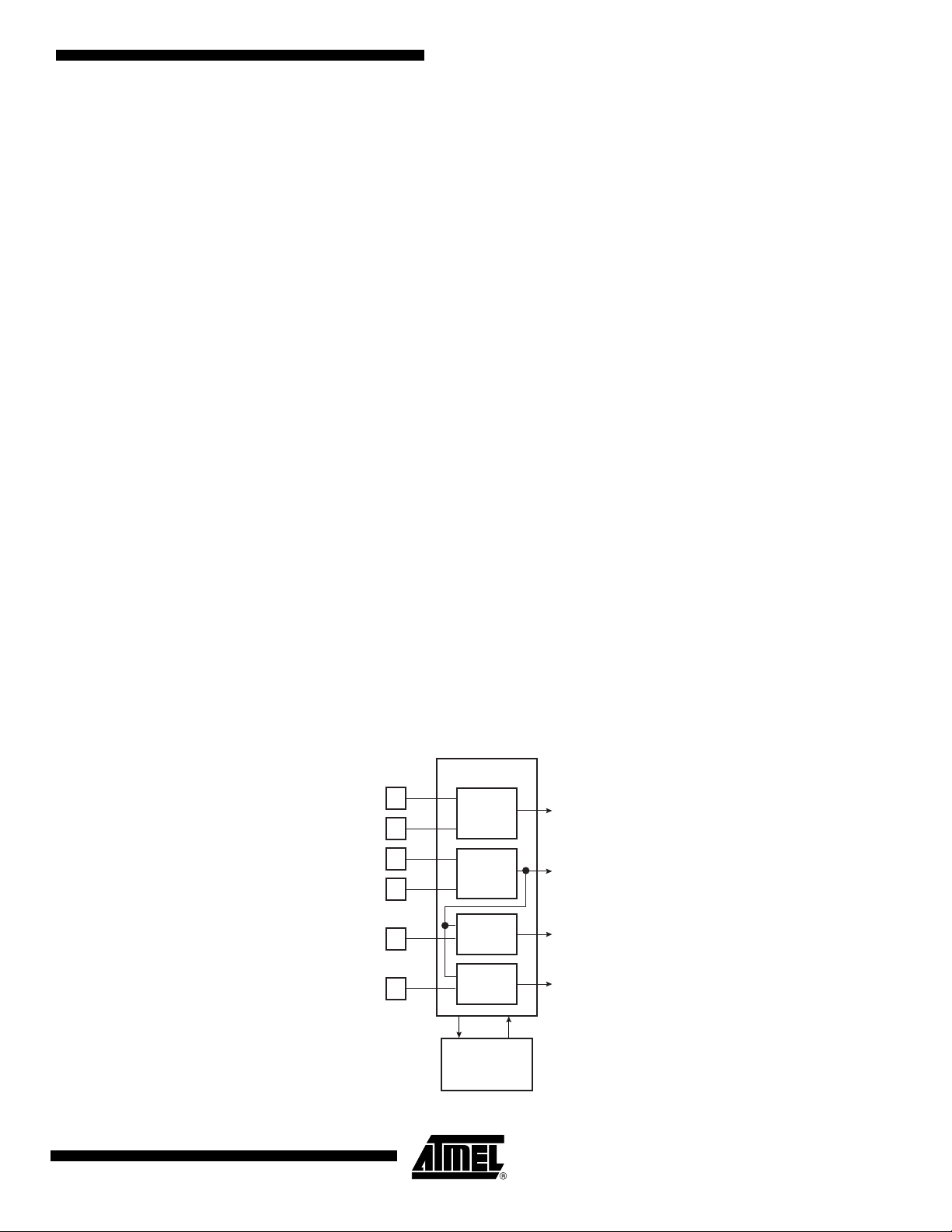
Figure 9-1. AT91CAP9S500A/AT91CAP9S250A System Controller Block Diagram
NRST
SHDN
WKUP
XIN32
XOUT32
XIN
XOUT
PLLRCA
PLLRCB
PA0-PA31
PB0-PB31
PC0-PC31
PD0-PD31
periph_irq[2..29]
pit_irq
rtt_irq
wdt_irq
dbgu_irq
pmc_irq
rstc_irq
periph_nreset
dbgu_rxd
periph_nreset
proc_nreset
VDDCORE
POR
VDDBU
POR
backup_nreset
SLOW
CLOCK
OSC
UTMI PLL
MAIN
OSC
PLLA
PLLB
periph_nreset
periph_nreset
periph_clk[2]
dbgu_rxd
irq0-irq1
fiq
MCK
MCK
debug
SLCK
debug
idle
SLCK
SLCK
SLCK
backup_nreset
SLCK
int
UDPHSCK
por_ntrst
jtag_nreset
rtt_alarm
MAINCK
PLLACK
PLLBCK
System Controller
Advanced
Interrupt
Controller
Debug
Unit
Periodic
Interval
Timer
Watchdog
Timer
wdt_fault
WDRPROC
Reset
Controller
Real-Time
Timer
Shut-Down
Controller
Power
Management
Controller
PIO
Controllers
VDDCORE Powered
int
dbgu_irq
dbgu_txd
pit_irq
wdt_irq
rstc_irq
periph_nreset
proc_nreset
backup_nreset
VDDBU Powered
rtt_irq
rtt_alarm
Voltage
Controller
battery_save
4 General-purpose
Backup Registers
periph_clk[2..31]
pck[0-3]
PCK
UHPCK
MCK
pmc_irq
idle
periph_irq[2]
irq0-irq1
fiq
dbgu_txd
por_ntrst
nirq
nfiq
ntrst
proc_nreset
PCK
debug
jtag_nreset
MCK
periph_nreset
UDPHSCK
periph_clk[28]
periph_nreset
periph_irq[28]
UHPCK
periph_clk[29]
periph_nreset
periph_irq[29]
periph_clk[7..31]
periph_nreset
periph_irq[7..27]
in
out
enable
ARM926EJ-S
Boundary Scan
TAP Controller
Bus Matrix
USB High-speed
Device Port
USB Host
Por t
Embedded
Peripherals
28
AT91CAP9S500A/AT91CAP9S250A
6264A–CAP–21-May-07
Page 29
9.2 Reset Controller
• Based on two Power-on-Reset cells
– One on VDDBU and one on VDDCORE
• Status of the last reset
– Either general reset (VDDBU rising), wake-up reset (VDDCORE rising), software
• Controls the internal resets and the NRST pin output
– Allows shaping a reset signal for the external devices
9.3 Shutdown Controller
• Shutdown and Wake-Up logic
– Software programmable assertion of the SHDN pin
– Deassertion Programmable on a WKUP pin level change or on alarm
9.4 Clock Generator
• Embeds the low power 32,768 Hz Slow Clock Oscillator
– Provides the permanent Slow Clock SLCK to the system
• Embeds the Main Oscillator
– Oscillator bypass feature
– Supports 8 to 16 MHz crystals
– 12 MHz crystal is required for USB High-Speed Device
• Embeds 2 PLLs
– Output 80 to 200 MHz clocks
– Integrates an input divider to increase output accuracy
– 1 MHz minimum input frequency
AT91CAP9S500A/AT91CAP9S250A
reset, user reset or watchdog reset
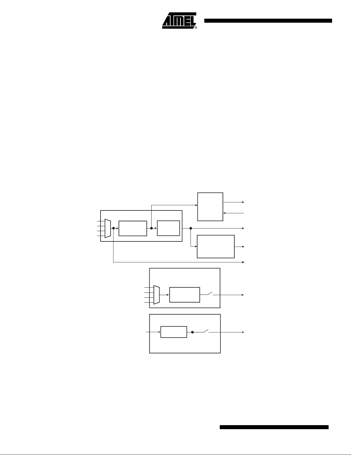
Figure 9-2. Clock Generator Block Diagram
XIN32
XOUT32
XIN
XOUT
PLLRCA
PLLRCB
6264A–CAP–21-May-07
Clock Generator
Slow Clock
Oscillator
Main
Oscillator
PLL and
Divider A
PLL and
Divider B
Power
Management
Controller
Slow Clock
SLCK
Main Clock
MAINCK
PLLA Clock
PLLACK
PLLB Clock
PLLBCK
ControlStatus
29
Page 30
9.5 Power Management Controller
•Provides:
– the Processor Clock PCK
– the Master Clock MCK, in particular to the Matrix and the memory interfaces
– the USB High-speed Device Clock UDPHSCK
– the USB Host Clock UHPCK
– independent peripheral clocks, typically at the frequency of MCK
– four programmable clock outputs: PCK0 to PCK3
• Five flexible operating modes:
– Normal Mode, processor and peripherals running at a programmable frequency
– Idle Mode, processor stopped waiting for an interrupt
– Slow Clock Mode, processor and peripherals running at low frequency
– Standby Mode, mix of Idle and Backup Mode, peripheral running at low frequency,
processor stopped waiting for an interrupt
– Backup Mode, Main Power Supplies off, VDDBU powered by a battery
Figure 9-3. AT91CAP9S500A/AT91CAP9S250A Power Management Controller Block Diagram
Processor
SLCK
MAINCK
PLLACK
PLLBCK
Master Clock Controller
Prescaler
/1,/2,/4,...,/64
Clock
Controller
Idle Mode
Divider
/1,/2,/4
Peripherals
Clock Controller
ON/OFF
Programmable Clock Controller
PCK
int
MCK
periph_clk[..]
DDRCK
9.6 Periodic Interval Timer
• Includes a 20-bit Periodic Counter, with less than 1 µs accuracy
• Includes a 12-bit Interval Overlay Counter
• Real-time OS or Linux/WinCE compliant tick generator
30
AT91CAP9S500A/AT91CAP9S250A
SLCK
MAINCK
PLLACK
PLLBCK
PLLBCK
Prescaler
/1,/2,/4,...,/64
USB Clock Controller
Divider
/1,/2,/4
ON/OFF
ON/OFF
pck[..]
UHPCK
6264A–CAP–21-May-07
Page 31

AT91CAP9S500A/AT91CAP9S250A
9.7 Watchdog Timer
• 16-bit key-protected only-once-Programmable Counter
• Windowed, prevents the processor to be in a dead-lock on the watchdog access
9.8 Real-time Timer
• Two Real-time Timers, allowing backup of time with different accuracies
– 32-bit Free-running back-up Counter
– Integrates a 16-bit programmable prescaler running on the embedded 32,768 Hz
oscillator
– Alarm Register to generate a wake-up of the system through the Shutdown
Controller
9.9 General-Purpose Backed-up Registers
• Four 32-bit backup general-purpose registers
9.10 Advanced Interrupt Controller
• Controls the interrupt lines (nIRQ and nFIQ) of the ARM Processor
• Thirty-two individually maskable and vectored interrupt sources
– Source 0 is reserved for the Fast Interrupt Input (FIQ)
– Source 1 is reserved for system peripherals (PIT, RTT, PMC, DBGU, etc.)
– Programmable Edge-triggered or Level-sensitive Internal Sources
– Programmable Positive/Negative Edge-triggered or High/Low Level-sensitive
• Four External Sources plus the Fast Interrupt signal
• 8-level Priority Controller
– Drives the Normal Interrupt of the processor
– Handles priority of the interrupt sources 1 to 31
– Higher priority interrupts can be served during service of lower priority interrupt
• Vectoring
– Optimizes Interrupt Service Routine Branch and Execution
– One 32-bit Vector Register per interrupt source
– Interrupt Vector Register reads the corresponding current Interrupt Vector
•Protect Mode
– Easy debugging by preventing automatic operations when protect models are
enabled
•Fast Forcing
– Permits redirecting any normal interrupt source on the Fast Interrupt of the
processor
9.11 Debug Unit
6264A–CAP–21-May-07
• Composed of two functions
–Two-pin UART
– Debug Communication Channel (DCC) support
31
Page 32

•Two-pin UART
• Debug Communication Channel Support
9.12 Chip Identification
• Chip ID: 0x039A03A0
• JTAG ID: 0x05B1B03F
• ARM926 TAP ID: 0x0792603F
9.13 PIO Controllers
• 4 PIO Controllers, PIOA to PIOD, controlling a total of 128 I/O Lines
• Each PIO Controller controls up to 32 programmable I/O Lines
• Fully programmable through Set/Clear Registers
• Multiplexing of two peripheral functions per I/O Line
• For each I/O Line (whether assigned to a peripheral or used as general purpose I/O)
• Synchronous output, provides Set and Clear of several I/O lines in a single write
– Implemented features are 100% compatible with the standard Atmel USART
– Independent receiver and transmitter with a common programmable Baud Rate
Generator
– Even, Odd, Mark or Space Parity Generation
– Parity, Framing and Overrun Error Detection
– Automatic Echo, Local Loopback and Remote Loopback Channel Modes
– Support for two PDC channels with connection to receiver and transmitter
– Offers visibility of and interrupt trigger from COMMRX and COMMTX signals from
the ARM Processor’s ICE Interface
– PIOA has 32 I/O Lines
– PIOB has 32 I/O Lines
– PIOC has 32 I/O Lines
– PIOD has 32 I/O Lines
– Input change interrupt
– Glitch filter
– Multi-drive option enables driving in open drain
– Programmable pull up on each I/O line
– Pin data status register, supplies visibility of the level on the pin at any time
32
AT91CAP9S500A/AT91CAP9S250A
6264A–CAP–21-May-07
Page 33

10. Peripherals
10.1 User Interface
10.2 Identifiers
AT91CAP9S500A/AT91CAP9S250A
The peripherals are mapped in the upper 256 Mbytes of the address space between the
addresses 0xFFFA 0000 and 0xFFFC FFFF. Each user peripheral is allocated 16 Kbytes of
address space.
A complete memory map is presented in Figure 8-1 on page 22.
The AT91CAP9S500A/AT91CAP9S250A embeds a wide range of peripherals. Table 10-1
defines the Peripheral Identifiers of the AT91CAP9S500A/AT91CAP9S250A. A peripheral identifier is required for the control of the peripheral interrupt with the Advanced Interrupt Controller
and for the control of the peripheral clock with the Power Management Controller.
Table 10-1. AT91CAP9S500A/AT91CAP9S250A Peripheral Identifiers
Peripheral
ID
0 AIC Advanced Interrupt Controller FIQ
1 SYSC System Controller Interrupt
2 PIOA-D Parallel I/O Controller A to D
3 MPB0 MP Block Peripheral 0
4 MPB1 MP Block Peripheral 1
5 MPB2 MP Block Peripheral 2
6 MPB3 MP Block Peripheral 3
7 MPB4 MP Block Peripheral 4
8 US0 USART 0
9 US1 USART 1
10 US2 USART 2
11 MCI0 Multimedia Card Interface 0
12 MCI1 Multimedia Card Interface 1
13 CAN CAN Controller
14 TWI Two-Wire Interface
15 SPI0 Serial Peripheral Interface 0
Peripheral
Mnemonic Peripheral Name
External
Interrupt
6264A–CAP–21-May-07
16 SPI1 Serial Peripheral Interface 1
17 SSC0 Synchronous Serial Controller 0
18 SSC1 Synchronous Serial Controller 1
19 AC97 AC97 Controller
20 TC0, TC1, TC2 Timer/Counter 0, 1 and 2
21 PWMC Pulse Width Modulation Controller
22 EMAC Ethernet MAC
23 Reserved Reserved
33
Page 34

Table 10-1. AT91CAP9S500A/AT91CAP9S250A Peripheral Identifiers (Continued)
Peripheral
ID
24 ADCC ADC Controller
25 ISI Image Sensor Interface
26 LCDC LCD Controller
27 DMA DMA Controller
28 UDPHS USB High Speed Device Port
29 UHP USB Host Port
30 AIC Advanced Interrupt Controller IRQ0
31 AIC Advanced Interrupt Controller IRQ1
Peripheral
Mnemonic Peripheral Name
10.2.1 Peripheral Interrupts and Clock Control
10.2.1.1 System Interrupt
The System Interrupt in Source 1 is the wired-OR of the interrupt signals coming from:
• the DDR/SDRAM Controller
• the BCRAM Controller
• the Debug Unit
• the Periodic Interval Timer
• the Real-Time Timer
• the Watchdog Timer
• the Reset Controller
• the Power Management Controller
• the MP Block
The clock of these peripherals cannot be deactivated and Peripheral ID 1 can only be used
within the Advanced Interrupt Controller.
External
Interrupt
10.2.1.2 External Interrupts
All external interrupt signals, i.e., the Fast Interrupt signal FIQ or the Interrupt signals IRQ0 to
IRQ1, use a dedicated Peripheral ID. However, there is no clock control associated with these
peripheral IDs.
10.2.1.3 Timer Counter Interrupts
The three Timer Counter channels interrupt signals are OR-wired together to provide the interrupt source 19 of the Advanced Interrupt Controller. This forces the programmer to read all
Timer Counter status registers before branching the right Interrupt Service Routine.
The Timer Counter channels clocks cannot be deactivated independently. Switching off the
clock of the Peripheral 19 disables the clock of the 3 channels.
34
AT91CAP9S500A/AT91CAP9S250A
6264A–CAP–21-May-07
Page 35

AT91CAP9S500A/AT91CAP9S250A
10.3 Peripherals Signals Multiplexing on I/O Lines
The AT91CAP9S500A/AT91CAP9S250A features 4 PIO controllers, PIOA, PIOB, PIOC and
PIOD, that multiplex the I/O lines of the peripheral set.
Each PIO Controller controls up to 32 lines. Each line can be assigned to one of two peripheral
functions, A or B. The multiplexing tables in the following paragraphs define how the I/O lines of
the peripherals A and B are multiplexed on the PIO Controllers. The two columns “Function” and
“Comments” have been inserted in this table for the user’s own comments; they may be used to
track how pins are defined in an application.
Note that some peripheral functions which are output only may be duplicated within both tables.
The column “Reset State” indicates whether the PIO Line resets in I/O mode or in peripheral
mode. If I/O is mentioned, the PIO Line resets in input with the pull-up enabled, so that the
device is maintained in a static state as soon as the reset is released. As a result, the bit corresponding to the PIO Line in the register PIO_PSR (Peripheral Status Register) resets low.
If a signal name is mentioned in the “Reset State” column, the PIO Line is assigned to this function and the corresponding bit in PIO_PSR resets high. This is the case of pins controlling
memories, in particular the address lines, which require the pin to be driven as soon as the reset
is released. Note that the pull-up resistor is also enabled in this case.
6264A–CAP–21-May-07
35
Page 36

10.3.1 PIO Controller A Multiplexing
Table 10-2. Multiplexing on PIO Controller A
PIO Controller A Application Usage
Reset
I/O Line Peripheral A Peripheral B Comments
PA0 MCI0_D0 SPI0_MISO I/O VDDIOP0
PA1 MCI0_CD SPI0_MOSI I/O VDDIOP0
PA2 MCI0_CK SPI0_SPCK I/O VDDIOP0
PA3 MCI0_D1 SPI0_NPCS1 I/O VDDIOP0
PA4 MCI0_D2 SPI0_NPCS2 I/O VDDIOP0
PA5 MCI0_D3 SPI0_NPCS0 I/O VDDIOP0
PA6 AC97FS I/O VDDIOP0
PA7 AC97CK I/O VDDIOP0
PA8 AC97TX I/O VDDIOP0
PA9 AC97RX I/O VDDIOP0
PA10 IRQ0 PWM1 I/O VDDIOP0
PA11 DMARQ0 PWM3 I/O VDDIOP0
PA12 CANTX PCK0 I/O VDDIOP0
PA13 CANRX I/O VDDIOP0
PA14 TCLK2 IRQ1 I/O VDDIOP0
PA15 DMARQ3 PCK2 I/O VDDIOP0
PA16 MCI1_CK ISI_D0 I/O VDDIOP1
PA17 MCI1_CD ISI_D1 I/O VDDIOP1
State
Power
Supply Function Comments
PA18 MCI1_D0 ISI_D2 I/O VDDIOP1
PA19 MCI1_D1 ISI_D3 I/O VDDIOP1
PA20 MCI1_D2 ISI_D4 I/O VDDIOP1
PA21 MCI1_D3 ISI_D5 I/O VDDIOP1
PA22 TXD0 ISI_D6 I/O VDDIOP1
PA23 RXD0 ISI_D7 I/O VDDIOP1
PA24 RTS0 ISI_PCK I/O VDDIOP1
PA25 CTS0 ISI_HSYNC I/O VDDIOP1
PA26 SCK0 ISI_VSYNC I/O VDDIOP1
PA27 PCK1 ISI_MCK I/O VDDIOP1
PA28 SPI0_NPCS3 ISI_D8 I/O VDDIOP1
PA29 TIOA0 ISI_D9 I/O VDDIOP1
PA30 TIOB0 ISI_D10 I/O VDDIOP1
PA31 DMARQ1 ISI_D11 I/O VDDIOP1
36
AT91CAP9S500A/AT91CAP9S250A
6264A–CAP–21-May-07
Page 37

10.3.2 PIO Controller B Multiplexing
Table 10-3. Multiplexing on PIO Controller B
PIO Controller B Application Usage
AT91CAP9S500A/AT91CAP9S250A
Reset
I/O Line Peripheral A Peripheral B Comments
PB0 TF0 I/O VDDIOP0
PB1 TK0 I/O VDDIOP0
PB2 TD0 I/O VDDIOP0
PB3 RD0 I/O VDDIOP0
PB4 RK0 TWD I/O VDDIOP0
PB5 RF0 TWCK I/O VDDIOP0
PB6 TF1 TIOA1 I/O VDDIOP0
PB7 TK1 TIOB1 I/O VDDIOP0
PB8 TD1 PWM2 I/O VDDIOP0
PB9 RD1 LCDCC I/O VDDIOP0
PB10 RK1 PCK1 I/O VDDIOP0
PB11 RF1 I/O VDDIOP0
PB12 SPI1_MISO I/O VDDIOP0
PB13 SPI1_MOSI AD0 I/O VDDIOP0
PB14 SPI1_SPCK AD1 I/O VDDIOP0
PB15 SPI1_NPCS0 AD2 I/O VDDIOP0
PB16 SPI1_NPCS1 AD3 I/O VDDIOP0
PB17 SPI1_NPCS2 AD4 I/O VDDIOP0
State
Power
Supply Function Comments
PB18 SPI1_NPCS3 AD5 I/O VDDIOP0
PB19 PWM0 AD6 I/O VDDIOP0
PB20 PWM1 AD7 I/O VDDIOP0
PB21 ETXCK/EREFCK TIOA2 I/O VDDIOP0
PB22 ERXDV TIOB2 I/O VDDIOP0
PB23 ETX0 PCK3 I/O VDDIOP0
PB24 ETX1 I/O VDDIOP0
PB25 ERX0 I/O VDDIOP0
PB26 ERX1 I/O VDDIOP0
PB27 ERXER I/O VDDIOP0
PB28 ETXEN TCLK0 I/O VDDIOP0
PB29 EMDC PWM3 I/O VDDIOP0
PB30 EMDIO I/O VDDIOP0
PB31 ADTRIG EF100 I/O VDDIOP0
6264A–CAP–21-May-07
37
Page 38

10.3.3 PIO Controller C Multiplexing
Table 10-4. Multiplexing on PIO Controller C
PIO Controller C Application Usage
Reset
I/O Line Peripheral A Peripheral B Comments
PC0 LCDVSYNC I/O VDDIOP0
PC1 LCDHSYNC I/O VDDIOP0
PC2 LCDDOTCK I/O VDDIOP0
PC3 LCDDEN PWM1 I/O VDDIOP0
PC4 LCDD0 LCDD3 I/O VDDIOP0
PC5 LCDD1 LCDD4 I/O VDDIOP0
PC6 LCDD2 LCDD5 I/O VDDIOP0
PC7 LCDD3 LCDD6 I/O VDDIOP0
PC8 LCDD4 LCDD7 I/O VDDIOP0
PC9 LCDD5 LCDD10 I/O VDDIOP0
PC10 LCDD6 LCDD11 I/O VDDIOP0
PC11 LCDD7 LCDD12 I/O VDDIOP0
PC12 LCDD8 LCDD13 I/O VDDIOP0
PC13 LCDD9 LCDD14 I/O VDDIOP0
PC14 LCDD10 LCDD15 I/O VDDIOP0
PC15 LCDD11 LCDD19 I/O VDDIOP0
PC16 LCDD12 LCDD20 I/O VDDIOP0
PC17 LCDD13 LCDD21 I/O VDDIOP0
State
Power
Supply Function Comments
PC18 LCDD14 LCDD22 I/O VDDIOP0
PC19 LCDD15 LCDD23 I/O VDDIOP0
PC20 LCDD16 ETX2 I/O VDDIOP0
PC21 LCDD17 ETX3 I/O VDDIOP0
PC22 LCDD18 ERX2 I/O VDDIOP0
PC23 LCDD19 ERX3 I/O VDDIOP0
PC24 LCDD20 ETXER I/O VDDIOP0
PC25 LCDD21 ECRS I/O VDDIOP0
PC26 LCDD22 ECOL I/O VDDIOP0
PC27 LCDD23 ERXCK I/O VDDIOP0
PC28 PWM0 TCLK1 I/O VDDIOP0
PC29 PCK0 PWM2 I/O VDDIOP0
PC30 DRXD I/O VDDIOP0
PC31 DTXD I/O VDDIOP0
38
AT91CAP9S500A/AT91CAP9S250A
6264A–CAP–21-May-07
Page 39

10.3.4 PIO Controller D Multiplexing
Table 10-5. Multiplexing on PIO Controller D
PIO Controller D Application Usage
AT91CAP9S500A/AT91CAP9S250A
Reset
I/O Line Peripheral A Peripheral B Comments
PD0 TXD1 SPI0_NPCS2 I/O VDDIOP0
PD1 RXD1 SPI0_NPCS3 I/O VDDIOP0
PD2 TXD2 SPI1_NPCS2 I/O VDDIOP0
PD3 RXD2 SPI1_NPCS3 I/O VDDIOP0
PD4 FIQ I/O VDDIOP0
PD5 DMARQ2 RTS2 I/O VDDIOP0
PD6 NWAIT CTS2 I/O VDDIOM
PD7 NCS4/CFCS0 RTS1 I/O VDDIOM
PD8 NCS5/CFCS1 CTS1 I/O VDDIOM
PD9 CFCE1 SCK2 I/O VDDIOM
PD10 CFCE2 SCK1 I/O VDDIOM
PD11 NCS2 I/O VDDIOM
PD12 A23 A23 VDDIOM
PD13 A24 A24 VDDIOM
PD14 A25/CFRNW A25 VDDIOM
PD15 NCS3/NANDCS I/O VDDIOM
PD16 D16 I/O VDDIOM
PD17 D17 I/O VDDIOM
State
Power
Supply Function Comments
PD18 D18 I/O VDDIOM
PD19 D19 I/O VDDIOM
PD20 D20 I/O VDDIOM
PD21 D21 I/O VDDIOM
PD22 D22 I/O VDDIOM
PD23 D23 I/O VDDIOM
PD24 D24 I/O VDDIOM
PD25 D25 I/O VDDIOM
PD26 D26 I/O VDDIOM
PD27 D27 I/O VDDIOM
PD28 D28 I/O VDDIOM
PD29 D29 I/O VDDIOM
PD30 D30 I/O VDDIOM
PD31 D31 I/O VDDIOM
6264A–CAP–21-May-07
39
Page 40

10.4 Embedded Peripherals
10.4.1 Serial Peripheral Interface
• Supports communication with serial external devices
– Four chip selects with external decoder support allow communication with up to 15
peripherals
– Serial memories, such as DataFlash and 3-wire EEPROMs
– Serial peripherals, such as ADCs, DACs, LCD Controllers, CAN Controllers and
Sensors
– External co-processors
• Master or slave serial peripheral bus interface
– 8- to 16-bit programmable data length per chip select
– Programmable phase and polarity per chip select
– Programmable transfer delays between consecutive transfers and between clock
and data per chip select
– Programmable delay between consecutive transfers
– Selectable mode fault detection
• Very fast transfers supported
– Transfers with baud rates up to MCK
– The chip select line may be left active to speed up transfers on the same device
10.4.2 Two-wire Interface
• Compatibility with standard two-wire serial memory
• One, two or three bytes for slave address
• Sequential read/write operations
10.4.3 USART
• Programmable Baud Rate Generator
• 5- to 9-bit full-duplex synchronous or asynchronous serial communications
• RS485 with driver control signal
• ISO7816, T = 0 or T = 1 Protocols for interfacing with smart cards
– 1, 1.5 or 2 stop bits in Asynchronous Mode or 1 or 2 stop bits in Synchronous Mode
– Parity generation and error detection
– Framing error detection, overrun error detection
– MSB- or LSB-first
– Optional break generation and detection
– By 8 or by-16 over-sampling receiver frequency
– Hardware handshaking RTS-CTS
– Receiver time-out and transmitter timeguard
– Optional Multi-drop Mode with address generation and detection
– Optional Manchester Encoding
– NACK handling, error counter with repetition and iteration limit
40
AT91CAP9S500A/AT91CAP9S250A
6264A–CAP–21-May-07
Page 41

• IrDA modulation and demodulation
– Communication at up to 115.2 Kbps
• Test Modes
– Remote Loopback, Local Loopback, Automatic Echo
10.4.4 Synchronous Serial Controller
• Provides serial synchronous communication links used in audio and telecom applications
(with CODECs in Master or Slave Modes, I
• Contains an independent receiver and transmitter and a common clock divider
• Offers a configurable frame sync and data length
• Receiver and transmitter can be programmed to start automatically or on detection of
different event on the frame sync signal
• Receiver and transmitter include a data signal, a clock signal and a frame synchronization
signal
10.4.5 AC97 Controller
• Compatible with AC97 Component Specification V2.2
• Capable to Interface with a Single Analog Front end
• Three independent RX Channels and three independent TX Channels
– One RX and one TX channel dedicated to the AC97 Analog Front end control
– One RX and one TX channel for data transfers, associated with a PDC
– One RX and one TX channel for data transfers with no PDC
• Time Slot Assigner allowing to assign up to 12 time slots to a channel
• Channels support mono or stereo up to 20 bit sample length
– Variable sampling rate AC97 Codec Interface (48KHz and below)
AT91CAP9S500A/AT91CAP9S250A
2
S, TDM Buses, Magnetic Card Reader, etc.)
10.4.6 Timer Counter
6264A–CAP–21-May-07
• Three 16-bit Timer Counter Channels
• Wide range of functions including:
– Frequency Measurement
– Event Counting
– Interval Measurement
– Pulse Generation
–Delay Timing
– Pulse Width Modulation
– Up/down Capabilities
• Each channel is user-configurable and contains:
– Three external clock inputs
– Five internal clock inputs
– Two multi-purpose input/output signals
• Two global registers that act on all three TC Channels
41
Page 42

10.4.7 Pulse Width Modulation Controller
• 4 channels, one 16-bit counter per channel
• Common clock generator, providing Thirteen Different Clocks
– A Modulo n counter providing eleven clocks
– Two independent Linear Dividers working on modulo n counter outputs
• Independent channel programming
– Independent Enable Disable Commands
– Independent Clock Selection
– Independent Period and Duty Cycle, with Double Bufferization
– Programmable selection of the output waveform polarity
– Programmable center or left aligned output waveform
10.4.8 Multimedia Card Interface
• 2 double-channel Multimedia Card Interface, allowing concurrent transfers with 2 cards
• Compatibility with MultiMedia Card Specification Version 3.31
• Compatibility with SD Memory Card Specification Version 1.0
• Compatibility with SDIO Specification Version V1.0.
• Cards clock rate up to Master Clock divided by 2
• Embedded power management to slow down clock rate when not used
• Each MCI has one slot supporting
– One MultiMediaCard bus (up to 30 cards) or
– One SD Memory Card
– One SDIO Card
• Support for stream, block and multi-block data read and write
10.4.9 CAN Controller
42
AT91CAP9S500A/AT91CAP9S250A
• Fully compliant with 16-mailbox CAN 2.0A and 2.0B CAN Controllers
• Bit rates up to 1Mbit/s.
• Object-oriented mailboxes, each with the following properties:
– CAN Specification 2.0 Part A or 2.0 Part B Programmable for Each Message
– Object Configurable as receive (with overwrite or not) or transmit
– Local Tag and Mask Filters up to 29-bit Identifier/Channel
– 32 bits access to Data registers for each mailbox data object
– Uses a 16-bit time stamp on receive and transmit message
– Hardware concatenation of ID unmasked bitfields to speedup family ID processing
– 16-bit internal timer for Time Stamping and Network synchronization
– Programmable reception buffer length up to 16 mailbox object
– Priority Management between transmission mailboxes
– Autobaud and listening mode
– Low power mode and programmable wake-up on bus activity or by the application
– Data, Remote, Error and Overload Frame handling
6264A–CAP–21-May-07
Page 43

10.4.10 USB Host Port
• Compliance with OHCI Rev 1.0 Specification
• Compliance with USB V2.0 Full-speed and Low-speed Specification
• Supports both Low-speed 1.5 Mbps and Full-speed 12 Mbps devices
• Root hub integrated with two downstream USB ports
• Two embedded USB transceivers
• Supports power management
• Operates as a master on the Matrix
• Internal DMA Controller, operating as a Master on Bus Matrix
10.4.11 USB High Speed Device Port
• USB V2.0 high-speed compliant, 480 MBits per second
• Embedded USB V2.0 UTMI+ high-speed transceiver
• Embedded 4K-byte dual-port RAM for endpoints
• Embedded 6 channels DMA controller
• Suspend/Resume logic
• Up to 2 or 3 banks for isochronous and bulk endpoints
• Seven endpoints:
– Endpoint 0: 64 bytes, 1 bank mode
– Endpoint 1 & 2: 512 bytes, 2 banks mode, HS isochronous capable
– Endpoint 3 & 4: 64 bytes, 3 banks mode
– Endpoint 5 & 6: 1024 bytes, 3 banks mode, HS isochronous capable
AT91CAP9S500A/AT91CAP9S250A
10.4.12 LCD Controller
• Single and Dual scan color and monochrome passive STN LCD panels supported
• Single scan active TFT LCD panels supported
• 4-bit single scan, 8-bit single or dual scan, 16-bit dual scan STN interfaces supported
• Up to 24-bit single scan TFT interfaces supported
• Up to 16 gray levels for mono STN and up to 4096 colors for color STN displays
• 1, 2 bits per pixel (palletized), 4 bits per pixel (non-palletized) for mono STN
• 1, 2, 4, 8 bits per pixel (palletized), 16 bits per pixel (non-palletized) for color STN
• 1, 2, 4, 8 bits per pixel (palletized), 16, 24 bits per pixel (non-palletized) for TFT
• Single clock domain architecture
• Resolution supported up to 2048x2048
• 2D-DMA Controller for management of virtual Frame Buffer
• Automatic resynchronization of the frame buffer pointer to prevent flickering
10.4.13 Ethernet 10/100 MAC
• Compatibility with IEEE Standard 802.3
• 10 and 100 MBits per second data throughput capability
– Allows management of frame buffer larger than the screen size and moving the view
over this virtual frame buffer
6264A–CAP–21-May-07
43
Page 44

• Full- and half-duplex operations
• MII or RMII interface to the physical layer
• Register Interface to address, data, status and control registers
• Internal DMA Controller, operating as a Master on Bus Matrix
• Interrupt generation to signal receive and transmit completion
• 28-byte transmit and 28-byte receive FIFOs
• Automatic pad and CRC generation on transmitted frames
• Address checking logic to recognize four 48-bit addresses
• Support promiscuous mode where all valid frames are copied to memory
• Support physical layer management through MDIO interface control of alarm and update
time/calendar data in
10.4.14 Image Sensor Interface
• ITU-R BT. 601/656 8-bit mode external interface support
• Support for ITU-R BT.656-4 SAV and EAV synchronization
• Vertical and horizontal resolutions up to 2048 x 2048
• Preview Path up to 640*480
• Support for packed data formatting for YCbCr 4:2:2 formats
• Preview scaler to generate smaller size image
• Programmable frame capture rate
• Internal DMA Controller, operating as a Master on Bus Matrix
44
AT91CAP9S500A/AT91CAP9S250A
6264A–CAP–21-May-07
Page 45

11. Metal Programmable Block
The Metal Programmable Block (MPBlock) is connected to internal resources as the AHB bus or
interrupts and to external resources as dedicated I/O pads or UTMI+ core.
The MPBlock may be used to implement the Advanced High-speed Bus (AHB) or Advanced
Peripheral Bus (APB) custom peripherals. The MPBlock adds approximately 500K or 250K
gates of standard cell custom logic to the AT91CAP9S500A/AT91CAP9S250A base design.
Figure 11-1 shows the MPBlock and its connections to internal or external resources.
Figure 11-1. MPBlock Connectivity
DMAITs
CLOCKS
CAN,
MACB, OHCI
ENABLE
AT91CAP9S500A/AT91CAP9S250A
AHB MASTERS AHB SLAVES
MPBlock Test Wrapper
MPBLOCK
500K Gates (CAP9500)
250K Gates (CAP9250)
DPR
512x36
10x
8x
CHIP ID
JTAG ID
11.1 Internal Connectivity
In order to connect the MPBlock custom peripheral to the AT91CAP9S500A/AT91CAP9S250A
base design, the following connections are made.
11.1.1 Clocks
The MPBlock receives the following clocks:
• 32,768 Hz Slow Clock
• 8 to 16 MHz Main Oscillator Clock
• PLLA Clock
• PLLB Clock
• 48 MHz USB Clock
• 12 MHz USB Clock
UTMI+
PHY
Chip Boundary Scan
MPIOA[31:0]
SPR
512x72
MPIOB[44:0]
6264A–CAP–21-May-07
45
Page 46

• 30 or 60 MHz UTMI+ USB Clock
• MCK System Clock
• DDRCK Dual Rate System Clock
• PCK Processor Clock
• 5 Gated Peripherals Clock (for AHB and/or APB peripherals) corresponding to Peripheral ID
11.1.2 AHB Master Buses
The MPBlock may implement up to three AHB masters, each having a dedicated AHB master
bus connected to the Bus Matrix.
11.1.3 AHB Slave Buses
The MPBlock receives four different AHB slave buses coming from the Bus Matrix. Each bus
has two or four select signals that can implement up to 12 AHB slaves.
11.1.4 Interrupts
The MPBlock is connected to 5 dedicated interrupt lines corresponding to Peripheral ID 3 to 9.
It is also connected to two other interrupt lines (through OR gate) corresponding to Peripheral ID
1 and 2
11.1.5 DMA Channels
The MPBlock is connected to 4 DMA hardware handshaking interfaces, allowing it to implement
up to 4 DMA enabled peripherals.
3 to 7
11.1.6 Peripheral DMA Channels
The MPBlock is not connected to the Peripheral DMA Controller. In order to implement Peripheral DMA Controller (PDC) enabled APB peripherals, a PDC and an AHB-to-APB Bridge must
be integrated into the MPBlock using one AHB master and one AHB slave bus.
11.1.7 MPBlock Single Port RAMs
The MPBlock is connected to eight instances of 512x72 High-Speed Single Port RAMs.
The MPBlock has control over all memory connections.
11.1.8 MPBlock Dual Port RAMs
The MPBlock is connected to ten instances of 512x36 High-Speed Dual Port RAMs.
The MPBlock has control over all memory connections.
11.1.9 Optional Peripherals Enable
The MPBlock drives the enable of the optional peripherals, and so can enable or disable any of
the optional peripherals.
46
AT91CAP9S500A/AT91CAP9S250A
6264A–CAP–21-May-07
Page 47

11.2 External Connectivity
The MPBlock is connected to the following external resources.
11.2.1 Dedicated I/O Lines
The MPBlock is directly connected to 77 (32 MPIOA and 45 MPIOB lines) dedicated I/O Pads
with the following features:
• Supply/Drive control pin (needed for high-speed or low voltage interfaces)
• Pull-up control pin
• Supported logic levels include:
– LVCMOS33 at 100 MHz maximum frequency
– LVCMOS25 at 50 MHz maximum frequency
– LVCMOS18 at 100 MHz maximum frequency
Only 32 dedicated I/O pins are available in the TFBGA324 package.
11.2.2 UTMI+ Transceiver
The MPBlock may be connected to the UTMI+ transceiver. As only one UTMI+ transceiver is
available, the USB High-speed Device and the MPBlock do not have access to the UTMI+ at the
same time. However, a dual role Master-Slave USB High-Speed may be implemented by using
the USB High-speed Device and integrating a High-speed Host in the MPBlock as the switching
between both is generated inside the MPBlock.
AT91CAP9S500A/AT91CAP9S250A
11.3 Prototyping Solution
In order to prototype the final custom design, a Prototyping Platform version of the
AT91CAP9S500A/AT91CAP9S250A design has been created. The platform maps APB and
AHB masters or slaves into the FPGA located outside the chip with the following features and
restrictions:
• AT91CAP9S500A/AT91CAP9S250A to FPGA interface is provided to prototype AHB masters
and slave into the external FPGA exactly as if it were in MPBlock.
• Prototyped AHB Masters
– Prototyped AHB Masters have access to AT91CAP9S500A/AT91CAP9S250A slave
– Prototyped AHB Masters have access to MPBlock (FPGA) slave resources.
• Prototyped AHB Slaves
– Prototyped AHB Slaves may be accessed from AT91CAP9S500A/AT91CAP9S250A
– Prototyped AHB Slaves may be accessed from MPBlock (FPGA) resources.
• Prototyped APB Slaves
– APB bus must be created locally in the FPGA by implementing AHB to APB bridge.
Figure 11-2 shows a typical prototyping solution.
resources.
master resources.
Peripheral DMA controller may also be necessary to implement locally in the FPGA
in order to prototype PDC enabled APB peripherals.
6264A–CAP–21-May-07
47
Page 48

Figure 11-2. Typical Prototyping Solution
MASTERS ARM926EJ-S
AT91CAP9S500A/AT91CAP9S250A
CAP9500
CAP9250
EBI
Bus Matrix
AHB 2 APB
BRIDGE
DPR
APB
SLAVE
4-channel
DMA
CAP9500/CAP9250 FPGA Interface
Local AHB Matrix
PDC
SLAVE
RAM
APB
APB
Metal Programmable Block
500K Gates (CAP9500)
250K Gates (CAP9250)
FPGA Interface
MPIOA[31:0] MPIOB[44:0]
AHB
MASTER
DPR
AHB
SLAVE
Emulation Area
FPGA
AHB
MASTER
DPR
MPBlock
6264A–CAP–21-May-07
48
Page 49

12. ARM926EJ-S Processor Overview
12.1 Overview
The ARM926EJ-S processor is a member of the ARM9™ family of general-purpose microprocessors. The ARM926EJ-S implements ARM architecture version 5TEJ and is targeted at multitasking applications where full memory management, high performance, low die size and low
power are all important features.
The ARM926EJ-S processor supports the 32-bit ARM and 16-bit Thumb instruction sets,
enabling the user to trade off between high performance and high code density. It also supports
8-bit Java instruction set and includes features for efficient execution of Java bytecode, providing a Java performance similar to a JIT (Just-In-Time compilers), for the next generation of Javapowered wireless and embedded devices. It includes an enhanced multiplier design for
improved DSP performance.
The ARM926EJ-S processor supports the ARM debug architecture and includes logic to assist
in both hardware and software debug.
The ARM926EJ-S provides a complete high performance processor subsystem, including:
• an ARM9EJ-S
• a Memory Management Unit (MMU)
• separate instruction and data AMBA
• separate instruction and data TCM interfaces
™
integer core
AT91CAP9S500A/AT91CAP9S250A
™
AHB bus interfaces
6264A–CAP–21-May-07
49
Page 50

12.2 Block Diagram
Figure 12-1. ARM926EJ-S Internal Functional Block Diagram
ARM926EJ-S
Coprocessor
Interface
TCM
Interface
EmbeddedICE
ICE
Interface
ETM
Interface
ARM9EJ-S
-RT
R DATAW DATA
Processor
INSTR
DA
IA
Droute
Iroute
DEXT
DCACHE
MMU
ICACHE
IEXT
Data
AHB
Interface
Bus
Interface
Unit
Instruction
AHB
Interface
AHB
AHB
12.3 ARM9EJ-S Processor
12.3.1 ARM9EJ-S Operating States
The ARM9EJ-S processor can operate in three different states, each with a specific instruction
set:
• ARM state: 32-bit, word-aligned ARM instructions.
• Thumb state: 16-bit, halfword-aligned Thumb instructions.
• Jazelle state: variable length, byte-aligned Jazelle instructions.
In Jazelle state, all instruction Fetches are in words.
12.3.2 Switching State
The operating state of the ARM9EJ-S core can be switched between:
• ARM state and Thumb state using the BX and BLX instructions, and loads to the PC
50
AT91CAP9S500A/AT91CAP9S250A
6264A–CAP–21-May-07
Page 51

• ARM state and Jazelle state using the BXJ instruction
All exceptions are entered, handled and exited in ARM state. If an exception occurs in Thumb or
Jazelle states, the processor reverts to ARM state. The transition back to Thumb or Jazelle
states occurs automatically on return from the exception handler.
12.3.3 Instruction Pipelines
The ARM9EJ-S core uses two kinds of pipelines to increase the speed of the flow of instructions
to the processor.
A five-stage (five clock cycles) pipeline is used for ARM and Thumb states. It consists of Fetch,
Decode, Execute, Memory and Writeback stages.
A six-stage (six clock cycles) pipeline is used for Jazelle state It consists of Fetch,
Jazelle/Decode (two clock cycles), Execute, Memory and Writeback stages.
12.3.4 Memory Access
The ARM9EJ-S core supports byte (8-bit), half-word (16-bit) and word (32-bit) access. Words
must be aligned to four-byte boundaries, half-words must be aligned to two-byte boundaries and
bytes can be placed on any byte boundary.
Because of the nature of the pipelines, it is possible for a value to be required for use before it
has been placed in the register bank by the actions of an earlier instruction. The ARM9EJ-S control logic automatically detects these cases and stalls the core or forward data.
AT91CAP9S500A/AT91CAP9S250A
12.3.5 Jazelle Technology
The Jazelle technology enables direct and efficient execution of Java byte codes on ARM processors, providing high performance for the next generation of Java-powered wireless and
embedded devices.
The new Java feature of ARM9EJ-S can be described as a hardware emulation of a JVM (Java
Virtual Machine). Java mode will appear as another state: instead of executing ARM or Thumb
instructions, it executes Java byte codes. The Java byte code decoder logic implemented in
ARM9EJ-S decodes 95% of executed byte codes and turns them into ARM instructions without
any overhead, while less frequently used byte codes are broken down into optimized sequences
of ARM instructions. The hardware/software split is invisible to the programmer, invisible to the
application and invisible to the operating system. All existing ARM registers are re-used in
Jazelle state and all registers then have particular functions in this mode.
Minimum interrupt latency is maintained across both ARM state and Java state. Since byte
codes execution can be restarted, an interrupt automatically triggers the core to switch from
Java state to ARM state for the execution of the interrupt handler. This means that no special
provision has to be made for handling interrupts while executing byte codes, whether in hardware or in software.
12.3.6 ARM9EJ-S Operating Modes
In all states, there are seven operation modes:
• User mode is the usual ARM program execution state. It is used for executing most
application programs
• Fast Interrupt (FIQ) mode is used for handling fast interrupts. It is suitable for high-speed data
transfer or channel process
• Interrupt (IRQ) mode is used for general-purpose interrupt handling
6264A–CAP–21-May-07
51
Page 52

• Supervisor mode is a protected mode for the operating system
• Abort mode is entered after a data or instruction prefetch abort
• System mode is a privileged user mode for the operating system
• Undefined mode is entered when an undefined instruction exception occurs
Mode changes may be made under software control, or may be brought about by external interrupts or exception processing. Most application programs execute in User Mode. The non-user
modes, known as privileged modes, are entered in order to service interrupts or exceptions or to
access protected resources.
12.3.7 ARM9EJ-S Registers
The ARM9EJ-S core has a total of 37 registers:
• 31 general-purpose 32-bit registers
• 6 32-bit status registers
Table 12-1 shows all the registers in all modes.
Table 12-1. ARM9TDMI
User and
System Mode
R0 R0 R0 R0 R0 R0
R1 R1 R1 R1 R1 R1
R2 R2 R2 R2 R2 R2
R3 R3 R3 R3 R3 R3
R4 R4 R4 R4 R4 R4
R5 R5 R5 R5 R5 R5
R6 R6 R6 R6 R6 R6
R7 R7 R7 R7 R7 R7
R8 R8 R8 R8 R8
R9 R9 R9 R9 R9
R10 R10 R10 R10 R10
R11 R11 R11 R11 R11
R12 R12 R12 R12 R12
R13 R13_SVC R13_ABORT R13_UNDEF R13_IRQ R13_FIQ
R14 R14_SVC R14_ABORT R14_UNDEF R14_IRQ R14_FIQ
PC PC PC PC PC PC
Supervisor
®
Modes and Registers Layout
Mode Abort Mode
Undefined
Mode Interrupt Mode
Fast Interrupt
Mode
R8_FIQ
R9_FIQ
R10_FIQ
R11_FIQ
R12_FIQ
52
CPSR CPSR CPSR CPSR CPSR CPSR
SPSR_SVC SPSR_ABORT SPSR_UNDEF SPSR_IRQ SPSR_FIQ
Mode-specific banked registers
The ARM state register set contains 16 directly-accessible registers, r0 to r15, and an additional
register, the Current Program Status Register (CPSR). Registers r0 to r13 are general-purpose
AT91CAP9S500A/AT91CAP9S250A
6264A–CAP–21-May-07
Page 53

AT91CAP9S500A/AT91CAP9S250A
registers used to hold either data or address values. Register r14 is used as a Link register that
holds a value (return address) of r15 when BL or BLX is executed. Register r15 is used as a program counter (PC), whereas the Current Program Status Register (CPSR) contains condition
code flags and the current mode bits.
In privileged modes (FIQ, Supervisor, Abort, IRQ, Undefined), mode-specific banked registers
(r8 to r14 in FIQ mode or r13 to r14 in the other modes) become available. The corresponding
banked registers r14_fiq, r14_svc, r14_abt, r14_irq, r14_und are similarly used to hold the values (return address for each mode) of r15 (PC) when interrupts and exceptions arise, or when
BL or BLX instructions are executed within interrupt or exception routines. There is another register called Saved Program Status Register (SPSR) that becomes available in privileged modes
instead of CPSR. This register contains condition code flags and the current mode bits saved as
a result of the exception that caused entry to the current (privileged) mode.
In all modes and due to a software agreement, register r13 is used as stack pointer.
The use and the function of all the registers described above should obey ARM Procedure Call
Standard (APCS) which defines:
• constraints on the use of registers
• stack conventions
• argument passing and result return
The Thumb state register set is a subset of the ARM state set. The programmer has direct
access to:
• Eight general-purpose registers r0-r7
• Stack pointer, SP
• Link register, LR (ARM r14)
•PC
• CPSR
There are banked registers SPs, LRs and SPSRs for each privileged mode (for more details see
the ARM9EJ-S Technical Reference Manual, ref. DDI0222B,
12.3.7.1 Status Registers
The ARM9EJ-S core contains one CPSR, and five SPSRs for exception handlers to use. The
program status registers:
• hold information about the most recently performed ALU operation
• control the enabling and disabling of interrupts
• set the processor operation mode
revision r1p2 page 2-12).
6264A–CAP–21-May-07
53
Page 54

Figure 12-2. Status Register Format
31 30 2928 27 24 7 6 5 0
NZCV Q JIFT
Reserved
Jazelle state bit
Reserved
Sticky Overflow
Overflow
Carry/Borrow/Extend
Zero
Negative/Less than
Mode
Mode bits
Thumb state bit
FIQ disable
IRQ disable
Figure 12-2 shows the status register format, where:
• N: Negative, Z: Zero, C: Carry, and V: Overflow are the four ALU flags
• The Sticky Overflow (Q) flag can be set by certain multiply and fractional arithmetic
instructions like QADD, QDADD, QSUB, QDSUB, SMLAxy, and SMLAWy needed to achieve
DSP operations.
The Q flag is sticky in that, when set by an instruction, it remains set until explicitly cleared by
an MSR instruction writing to the CPSR. Instructions cannot execute conditionally on the
status of the Q flag.
• The J bit in the CPSR indicates when the ARM9EJ-S core is in Jazelle state, where:
– J = 0: The processor is in ARM or Thumb state, depending on the T bit
– J = 1: The processor is in Jazelle state.
• Mode: five bits to encode the current processor mode
12.3.7.2 Exceptions
Exception Types and Priorities
The ARM9EJ-S supports five types of exceptions. Each type drives the ARM9EJ-S in a privi-
leged mode. The types of exceptions are:
• Fast interrupt (FIQ)
• Normal interrupt (IRQ)
• Data and Prefetched aborts (Abort)
• Undefined instruction (Undefined)
• Software interrupt and Reset (Supervisor)
When an exception occurs, the banked version of R14 and the SPSR for the exception mode
are used to save the state.
More than one exception can happen at a time, therefore the ARM9EJ-S takes the arisen exceptions according to the following priority order:
• Reset (highest priority)
• Data Abort
•FIQ
•IRQ
•Prefetch Abort
• BKPT, Undefined instruction, and Software Interrupt (SWI) (Lowest priority)
54
AT91CAP9S500A/AT91CAP9S250A
6264A–CAP–21-May-07
Page 55

The BKPT, or Undefined instruction, and SWI exceptions are mutually exclusive.
There is one exception in the priority scheme though, when FIQs are enabled and a Data Abort
occurs at the same time as an FIQ, the ARM9EJ-S core enters the Data Abort handler, and proceeds immediately to FIQ vector. A normal return from the FIQ causes the Data Abort handler to
resume execution. Data Aborts must have higher priority than FIQs to ensure that the transfer
error does not escape detection.
Exception Modes and Handling
Exceptions arise whenever the normal flow of a program must be halted temporarily, for example, to service an interrupt from a peripheral.
When handling an ARM exception, the ARM9EJ-S core performs the following operations:
1. Preserves the address of the next instruction in the appropriate Link Register that corresponds to the new mode that has been entered. When the exception entry is from:
– ARM and Jazelle states, the ARM9EJ-S copies the address of the next instruction
– THUMB state, the ARM9EJ-S writes the value of the PC into LR, offset by a value
2. Copies the CPSR into the appropriate SPSR.
3. Forces the CPSR mode bits to a value that depends on the exception.
4. Forces the PC to fetch the next instruction from the relevant exception vector.
The register r13 is also banked across exception modes to provide each exception handler with
private stack pointer.
AT91CAP9S500A/AT91CAP9S250A
into LR (current PC(r15) + 4 or PC + 8 depending on the exception).
(current PC + 2, PC + 4 or PC + 8 depending on the exception) that causes the
program to resume from the correct place on return.
The ARM9EJ-S can also set the interrupt disable flags to prevent otherwise unmanageable
nesting of exceptions.
When an exception has completed, the exception handler must move both the return value in
the banked LR minus an offset to the PC and the SPSR to the CPSR. The offset value varies
according to the type of exception. This action restores both PC and the CPSR.
The fast interrupt mode has seven private registers r8 to r14 (banked registers) to reduce or
remove the requirement for register saving which minimizes the overhead of context switching.
The Prefetch Abort is one of the aborts that indicates that the current memory access cannot be
completed. When a Prefetch Abort occurs, the ARM9EJ-S marks the prefetched instruction as
invalid, but does not take the exception until the instruction reaches the Execute stage in the
pipeline. If the instruction is not executed, for example because a branch occurs while it is in the
pipeline, the abort does not take place.
The breakpoint (BKPT) instruction is a new feature of ARM9EJ-S that is destined to solve the
problem of the Prefetch Abort. A breakpoint instruction operates as though the instruction
caused a Prefetch Abort.
A breakpoint instruction does not cause the ARM9EJ-S to take the Prefetch Abort exception until
the instruction reaches the Execute stage of the pipeline. If the instruction is not executed, for
example because a branch occurs while it is in the pipeline, the breakpoint does not take place.
12.3.8 ARM Instruction Set Overview
The ARM instruction set is divided into:
6264A–CAP–21-May-07
• Branch instructions
55
Page 56

• Data processing instructions
• Status register transfer instructions
• Load and Store instructions
• Coprocessor instructions
• Exception-generating instructions
ARM instructions can be executed conditionally. Every instruction contains a 4-bit condition
code field (bits[31:28]).
Table 12-2 gives the ARM instruction mnemonic list.
Table 12-2. ARM Instruction Mnemonic List
Mnemonic Operation Mnemonic Operation
MOV Move MVN Move Not
ADD Add ADC Add with Carry
SUB Subtract SBC Subtract with Carry
RSB Reverse Subtract RSC Reverse Subtract with Carry
CMP Compare CMN Compare Negated
TST Test TEQ Test Equivalence
AND Logical AND BIC Bit Clear
EOR Logical Exclusive OR ORR Logical (inclusive) OR
MUL Multiply MLA Multiply Accumulate
SMULL Sign Long Multiply UMULL Unsigned Long Multiply
SMLAL
MSR Move to Status Register MRS Move From Status Register
B Branch BL Branch and Link
BX Branch and Exchange SWI Software Interrupt
LDR Load Word STR Store Word
LDRSH Load Signed Halfword
LDRSB Load Signed Byte
LDRH Load Half Word STRH Store Half Word
LDRB Load Byte STRB Store Byte
LDRBT
LDRT Load Register with Translation STRT Store Register with Translation
LDM Load Multiple STM Store Multiple
SWP Swap Word SWPB Swap Byte
MCR Move To Coprocessor MRC Move From Coprocessor
LDC Load To Coprocessor STC Store From Coprocessor
CDP Coprocessor Data Processing
Signed Long Multiply
Accumulate
Load Register Byte with
Translation
UMLAL
STRBT
Unsigned Long Multiply
Accumulate
Store Register Byte with
Translation
56
AT91CAP9S500A/AT91CAP9S250A
6264A–CAP–21-May-07
Page 57

12.3.9 New ARM Instruction Set
.
Table 12-3. New ARM Instruction Mnemonic List
Mnemonic Operation Mnemonic Operation
BXJ Branch and exchange to Java MRRC Move double from coprocessor
(1)
BLX
SMLAxy
SMLAL
SMLAWy
SMULxy Signed Multiply 16 * 16 bit PLD
SMULWy Signed Multiply 32 * 16 bit STRD Store Double
QADD Saturated Add STC2
QDADD Saturated Add with Double LDRD Load Double
QSUB Saturated subtract LDC2
QDSUB Saturated Subtract with double CLZ Count Leading Zeroes
AT91CAP9S500A/AT91CAP9S250A
Branch, Link and exchange MCR2
Signed Multiply Accumulate 16 *
16 bit
Signed Multiply Accumulate
Long
Signed Multiply Accumulate 32 *
16 bit
MCRR Move double to coprocessor
CDP2
BKPT Breakpoint
Alternative move of ARM reg to
coprocessor
Alternative Coprocessor Data
Processing
Soft Preload, Memory prepare to
load from address
Alternative Store from
Coprocessor
Alternative Load to
Coprocessor
Notes: 1. A Thumb BLX contains two consecutive Thumb instructions, and takes four cycles.
12.3.10 Thumb Instruction Set Overview
The Thumb instruction set is a re-encoded subset of the ARM instruction set.
The Thumb instruction set is divided into:
• Branch instructions
• Data processing instructions
• Load and Store instructions
• Load and Store multiple instructions
• Exception-generating instruction
Table 5 shows the Thumb instruction set. Table 12-4 gives the Thumb instruction mnemonic list.
Table 12-4. Thumb Instruction Mnemonic List
Mnemonic Operation Mnemonic Operation
MOV Move MVN Move Not
ADD Add ADC Add with Carry
SUB Subtract SBC Subtract with Carry
CMP Compare CMN Compare Negated
TST Test NEG Negate
AND Logical AND BIC Bit Clear
EOR Logical Exclusive OR ORR Logical (inclusive) OR
6264A–CAP–21-May-07
57
Page 58

Table 12-4. Thumb Instruction Mnemonic List (Continued)
Mnemonic Operation Mnemonic Operation
LSL Logical Shift Left LSR Logical Shift Right
ASR Arithmetic Shift Right ROR Rotate Right
MUL Multiply BLX Branch, Link, and Exchange
B Branch BL Branch and Link
BX Branch and Exchange SWI Software Interrupt
LDR Load Word STR Store Word
LDRH Load Half Word STRH Store Half Word
LDRB Load Byte STRB Store Byte
LDRSH Load Signed Halfword LDRSB Load Signed Byte
LDMIA Load Multiple STMIA Store Multiple
PUSH Push Register to stack POP Pop Register from stack
BCC Conditional Branch BKPT Breakpoint
12.4 CP15 Coprocessor
Coprocessor 15, or System Control Coprocessor CP15, is used to configure and control all the
items in the list below:
• ARM9EJ-S
• Caches (ICache, DCache and write buffer)
•TCM
•MMU
• Other system options
To control these features, CP15 provides 16 additional registers. See Table 12-5.
58
Table 12-5. CP15 Registers
Register Name Read/Write
0 ID Code
0 Cache type
0 TCM status
(1)
(1)
(1)
1 Control Read/write
2 Translation Table Base Read/write
3 Domain Access Control Read/write
4 Reserved None
5 Data fault Status
5 Instruction fault status
(1)
(1)
6 Fault Address Read/write
7 Cache Operations Read/Write
8 TLB operations Unpredictable/Write
AT91CAP9S500A/AT91CAP9S250A
Read/Unpredictable
Read/Unpredictable
Read/Unpredictable
Read/write
Read/write
6264A–CAP–21-May-07
Page 59

AT91CAP9S500A/AT91CAP9S250A
Table 12-5. CP15 Registers
Register Name Read/Write
9 cache lockdown
9 TCM region Read/write
10 TLB lockdown Read/write
11 Reserved None
12 Reserved None
13 FCSE PID
13 Context ID
14 Reserved None
15 Test configuration Read/Write
Notes: 1. Register locations 0,5, and 13 each provide access to more than one register. The register
accessed depends on the value of the opcode_2 field.
2. Register location 9 provides access to more than one register. The register accessed depends
on the value of the CRm field.
(2)
(1)
(1)
Read/write
Read/write
Read/Write
6264A–CAP–21-May-07
59
Page 60

12.4.1 CP15 Registers Access
CP15 registers can only be accessed in privileged mode by:
• MCR (Move to Coprocessor from ARM Register) instruction is used to write an ARM register
to CP15.
• MRC (Move to ARM Register from Coprocessor) instruction is used to read the value of
CP15 to an ARM register.
Other instructions like CDP, LDC, STC can cause an undefined instruction exception.
The assembler code for these instructions is:
MCR/MRC{cond} p15, opcode_1, Rd, CRn, CRm, opcode_2.
The MCR, MRC instructions bit pattern is shown below:
31 30 29 28 27 26 25 24
cond 1110
23 22 21 20 19 18 17 16
opcode_1 L CRn
15 14 13 12 11 10 9 8
Rd 1111
76543210
opcode_2 1 CRm
• CRm[3:0]: Specified Coprocessor Action
Determines specific coprocessor action. Its value is dependent on the CP15 register used. For details, refer to CP15 specific register behavior.
• opcode_2[7:5]
Determines specific coprocessor operation code. By default, set to 0.
• Rd[15:12]: ARM Register
Defines the ARM register whose value is transferred to the coprocessor. If R15 is chosen, the result is unpredictable.
• CRn[19:16]: Coprocessor Register
Determines the destination coprocessor register.
• L: Instruction Bit
0 = MCR instruction
1 = MRC instruction
• opcode_1[23:20]: Coprocessor Code
Defines the coprocessor specific code. Value is c15 for CP15.
• cond [31:28]: Condition
For more details, see Chapter 2 in ARM926EJ-S TRM, ref. DDI0198B.
60
AT91CAP9S500A/AT91CAP9S250A
6264A–CAP–21-May-07
Page 61

12.5 Memory Management Unit (MMU)
The ARM926EJ-S processor implements an enhanced ARM architecture v5 MMU to provide virtual memory features required by operating systems like Symbian
®
Linux
. These virtual memory features are memory access permission controls and virtual to
physical address translations.
The Virtual Address generated by the CPU core is converted to a Modified Virtual Address
(MVA) by the FCSE (Fast Context Switch Extension) using the value in CP15 register13. The
MMU translates modified virtual addresses to physical addresses by using a single, two-level
page table set stored in physical memory. Each entry in the set contains the access permissions
and the physical address that correspond to the virtual address.
The first level translation tables contain 4096 entries indexed by bits [31:20] of the MVA. These
entries contain a pointer to either a 1 MB section of physical memory along with attribute information (access permissions, domain, etc.) or an entry in the second level translation tables;
coarse table and fine table.
The second level translation tables contain two subtables, coarse table and fine table. An entry
in the coarse table contains a pointer to both large pages and small pages along with access
permissions. An entry in the fine table contains a pointer to large, small and tiny pages.
Table 7 shows the different attributes of each page in the physical memory.
AT91CAP9S500A/AT91CAP9S250A
®
OS, Windows CE®, and
Table 12-6. Mapping Details
Mapping Name Mapping Size Access Permission By Subpage Size
Section 1M byte Section -
Large Page 64K bytes 4 separated subpages 16K bytes
Small Page 4K bytes 4 separated subpages 1K byte
Tiny Page 1K byte Tiny Page -
The MMU consists of:
• Access control logic
• Translation Look-aside Buffer (TLB)
• Translation table walk hardware
12.5.1 Access Control Logic
The access control logic controls access information for every entry in the translation table. The
access control logic checks two pieces of access information: domain and access permissions.
The domain is the primary access control mechanism for a memory region; there are 16 of them.
It defines the conditions necessary for an access to proceed. The domain determines whether
the access permissions are used to qualify the access or whether they should be ignored.
The second access control mechanism is access permissions that are defined for sections and
for large, small and tiny pages. Sections and tiny pages have a single set of access permissions
whereas large and small pages can be associated with 4 sets of access permissions, one for
each subpage (quarter of a page).
6264A–CAP–21-May-07
61
Page 62

12.5.2 Translation Look-aside Buffer (TLB)
The Translation Look-aside Buffer (TLB) caches translated entries and thus avoids going
through the translation process every time. When the TLB contains an entry for the MVA (Modified Virtual Address), the access control logic determines if the access is permitted and outputs
the appropriate physical address corresponding to the MVA. If access is not permitted, the MMU
signals the CPU core to abort.
If the TLB does not contain an entry for the MVA, the translation table walk hardware is invoked
to retrieve the translation information from the translation table in physical memory.
12.5.3 Translation Table Walk Hardware
The translation table walk hardware is a logic that traverses the translation tables located in
physical memory, gets the physical address and access permissions and updates the TLB.
The number of stages in the hardware table walking is one or two depending whether the
address is marked as a section-mapped access or a page-mapped access.
There are three sizes of page-mapped accesses and one size of section-mapped access. Pagemapped accesses are for large pages, small pages and tiny pages. The translation process
always begins with a level one fetch. A section-mapped access requires only a level one fetch,
but a page-mapped access requires an additional level two fetch. For further details on the
MMU, please refer to chapter 3 in ARM926EJ-S Technical Reference Manual, ref. DDI0198B.
12.5.4 MMU Faults
The MMU generates an abort on the following types of faults:
• Alignment faults (for data accesses only)
• Translation faults
• Domain faults
• Permission faults
The access control mechanism of the MMU detects the conditions that produce these faults. If
the fault is a result of memory access, the MMU aborts the access and signals the fault to the
CPU core.The MMU retains status and address information about faults generated by the data
accesses in the data fault status register and fault address register. It also retains the status of
faults generated by instruction fetches in the instruction fault status register.
The fault status register (register 5 in CP15) indicates the cause of a data or prefetch abort, and
the domain number of the aborted access when it happens. The fault address register (register 6
in CP15) holds the MVA associated with the access that caused the Data Abort. For further
details on MMU faults, please refer to chapter 3 in ARM926EJ-S Technical Reference Manual,
ref. DDI0198B.
12.6 Caches and Write Buffer
The ARM926EJ-S contains a 16 KB Instruction Cache (ICache), a 16 KB Data Cache (DCache),
and a write buffer. Although the ICache and DCache share common features, each still has
some specific mechanisms.
The caches (ICache and DCache) are four-way set associative, addressed, indexed and tagged
using the Modified Virtual Address (MVA), with a cache line length of eight words with two dirty
bits for the DCache. The ICache and DCache provide mechanisms for cache lockdown, cache
pollution control, and line replacement.
62
AT91CAP9S500A/AT91CAP9S250A
6264A–CAP–21-May-07
Page 63

A new feature is now supported by ARM926EJ-S caches called allocate on read-miss commonly
known as wrapping. This feature enables the caches to perform critical word first cache refilling.
This means that when a request for a word causes a read-miss, the cache performs an AHB
access. Instead of loading the whole line (eight words), the cache loads the critical word first, so
the processor can reach it quickly, and then the remaining words, no matter where the word is
located in the line.
The caches and the write buffer are controlled by the CP15 register 1 (Control), CP15 register 7
(cache operations) and CP15 register 9 (cache lockdown).
12.6.1 Instruction Cache (ICache)
The ICache caches fetched instructions to be executed by the processor. The ICache can be
enabled by writing 1 to I bit of the CP15 Register 1 and disabled by writing 0 to this same bit.
When the MMU is enabled, all instruction fetches are subject to translation and permission
checks. If the MMU is disabled, all instructions fetches are cachable, no protection checks are
made and the physical address is flat-mapped to the modified virtual address. With the MVA use
disabled, context switching incurs ICache cleaning and/or invalidating.
When the ICache is disabled, all instruction fetches appear on external memory (AHB) (see
Tables 4-1 and 4-2 in page 4-4 in ARM926EJ-S TRM, ref. DDI0198B).
AT91CAP9S500A/AT91CAP9S250A
On reset, the ICache entries are invalidated and the ICache is disabled. For best performance,
ICache should be enabled as soon as possible after reset.
12.6.2 Data Cache (DCache) and Write Buffer
ARM926EJ-S includes a DCache and a write buffer to reduce the effect of main memory bandwidth and latency on data access performance. The operations of DCache and write buffer are
closely connected.
12.6.2.1 DCache
The DCache needs the MMU to be enabled. All data accesses are subject to MMU permission
and translation checks. Data accesses that are aborted by the MMU do not cause linefills or data
accesses to appear on the AMBA ASB interface. If the MMU is disabled, all data accesses are
noncachable, nonbufferable, with no protection checks, and appear on the AHB bus. All
addresses are flat-mapped, VA = MVA = PA, which incurs DCache cleaning and/or invalidating
every time a context switch occurs.
The DCache stores the Physical Address Tag (PA Tag) from which every line was loaded and
uses it when writing modified lines back to external memory. This means that the MMU is not
involved in write-back operations.
Each line (8 words) in the DCache has two dirty bits, one for the first four words and the other
one for the second four words. These bits, if set, mark the associated half-lines as dirty. If the
cache line is replaced due to a linefill or a cache clean operation, the dirty bits are used to decide
whether all, half or none is written back to memory.
6264A–CAP–21-May-07
DCache can be enabled or disabled by writing either 1 or 0 to bit C in register 1 of CP15 (see
Tables 4-3 and 4-4 on page 4-5 in ARM926EJ-S TRM, ref. DDI0222B).
The DCache supports write-through and write-back cache operations, selected by memory
region using the C and B bits in the MMU translation tables.
63
Page 64

12.6.2.2 Write Buffer
Write-though Operation
The DCache contains an eight data word entry, single address entry write-back buffer used to
hold write-back data for cache line eviction or cleaning of dirty cache lines.
The Write Buffer can hold up to 16 words of data and four separate addresses. DCache and
Write Buffer operations are closely connected as their configuration is set in each section by the
page descriptor in the MMU translation table.
The ARM926EJ-S contains a write buffer that has a 16-word data buffer and a four- address
buffer. The write buffer is used for all writes to a bufferable region, write-through region and
write-back region. It also allows to avoid stalling the processor when writes to external memory
are performed. When a store occurs, data is written to the write buffer at core speed (high
speed). The write buffer then completes the store to external memory at bus speed (typically
slower than the core speed). During this time, the ARM9EJ-S processor can preform other
tasks.
DCache and Write Buffer support write-back and write-through memory regions, controlled by C
and B bits in each section and page descriptor within the MMU translation tables.
When a cache write hit occurs, the DCache line is updated. The updated data is then written to
the write buffer which transfers it to external memory.
When a cache write miss occurs, a line, chosen by round robin or another algorithm, is stored in
the write buffer which transfers it to external memory.
Write-back Operation
When a cache write hit occurs, the cache line or half line is marked as dirty, meaning that its
contents are not up-to-date with those in the external memory.
When a cache write miss occurs, a line, chosen by round robin or another algorithm, is stored in
the write buffer which transfers it to external memory.
12.7 Tightly-Coupled Memory Interface
12.7.1 TCM Description
The ARM926EJ-S processor features a Tightly-Coupled Memory (TCM) interface, which
enables separate instruction and data TCMs (ITCM and DTCM) to be directly reached by the
processor. TCMs are used to store real-time and performance critical code, they also provide a
DMA support mechanism. Unlike AHB accesses to external memories, accesses to TCMs are
fast and deterministic and do not incur bus penalties.
The user has the possibility to independently configure each TCM size with values within the following ranges, [0KB, 0 KB] for ITCM size and [0KB, 0 KB] for DTCM size.
TCMs can be configured by two means: HMATRIX TCM register and TCM region register (register 9) in CP15 and both steps should be performed. HMATRIX TCM register sets TCM size
whereas TCM region register (register 9) in CP15 maps TCMs and enables them.
The data side of the ARM9EJ-S core is able to access the ITCM. This is necessary to enable
code to be loaded into the ITCM, for SWI and emulated instruction handlers, and for accesses to
PC-relative literal pools.
64
AT91CAP9S500A/AT91CAP9S250A
6264A–CAP–21-May-07
Page 65

12.7.2 Enabling and Disabling TCMs
Prior to any enabling step, the user should configure the TCM sizes in HMATRIX TCM register.
Then enabling TCMs is performed by using TCM region register (register 9) in CP15. The user
should use the same sizes as those put in HMATRIX TCM register. For further details and programming tips, please refer to chapter 2.3 in ARM926EJ-S TRM, ref. DDI0222B.
12.7.3 TCM Mapping
The TCMs can be located anywhere in the memory map, with a single region available for ITCM
and a separate region available for DTCM. The TCMs are physically addressed and can be
placed anywhere in physical address space. However, the base address of a TCM must be
aligned to its size, and the DTCM and ITCM regions must not overlap. TCM mapping is performed by using TCM region register (register 9) in CP15. The user should input the right
mapping address for TCMs.
12.8 Bus Interface Unit
The ARM926EJ-S features a Bus Interface Unit (BIU) that arbitrates and schedules AHB
requests. The BIU implements a multi-layer AHB, based on the AHB-Lite protocol, that enables
parallel access paths between multiple AHB masters and slaves in a system. This is achieved by
using a more complex interconnection matrix and gives the benefit of increased overall bus
bandwidth, and a more flexible system architecture.
AT91CAP9S500A/AT91CAP9S250A
The multi-master bus architecture has a number of benefits:
• It allows the development of multi-master systems with an increased bus bandwidth and a
flexible architecture.
• Each AHB layer becomes simple because it only has one master, so no arbitration or masterto-slave muxing is required. AHB layers, implementing AHB-Lite protocol, do not have to
support request and grant, nor do they have to support retry and split transactions.
• The arbitration becomes effective when more than one master wants to access the same
slave simultaneously.
12.8.1 Supported Transfers
The ARM926EJ-S processor performs all AHB accesses as single word, bursts of four words, or
bursts of eight words. Any ARM9EJ-S core request that is not 1, 4, 8 words in size is split into
packets of these sizes. Note that the Atmel bus is AHB-Lite protocol compliant, hence it does not
support split and retry requests.
6264A–CAP–21-May-07
65
Page 66

Table 8 gives an overview of the supported transfers and different kinds of transactions they are
used for.
Table 12-7. Supported Transfers
HBurst[2:0] Description
SINGLE Single transfer
Single transfer of word, half word, or byte:
• data write (NCNB, NCB, WT, or WB that has missed in DCache)
• data read (NCNB or NCB)
• NC instruction fetch (prefetched and non-prefetched)
• page table walk read
INCR4 Four-word incrementing burst
INCR8 Eight-word incrementing burst Full-line cache write-back, eight-word burst NCNB, NCB, WT, or WB write.
WRAP8 Eight-word wrapping burst Cache linefill
Half-line cache write-back, Instruction prefetch, if enabled. Four-word burst NCNB,
NCB, WT, or WB write.
12.8.2 Thumb Instruction Fetches
All instructions fetches, regardless of the state of ARM9EJ-S core, are made as 32-bit accesses
on the AHB. If the ARM9EJ-S is in Thumb state, then two instructions can be fetched at a time.
12.8.3 Address Alignment
The ARM926EJ-S BIU performs address alignment checking and aligns AHB addresses to the
necessary boundary. 16-bit accesses are aligned to halfword boundaries, and 32-bit accesses
are aligned to word boundaries.
66
AT91CAP9S500A/AT91CAP9S250A
6264A–CAP–21-May-07
Page 67

13. Debug and Test
13.1 Description
AT91CAP9S500A/AT91CAP9S250A
The AT91CAP9 features a number of complementary debug and test capabilities. A common
JTAG/ICE (In-Circuit Emulator) port is used for standard debugging functions, such as downloading code and single-stepping through programs. The Debug Unit provides a two-pin UART
that can be used to upload an application into internal SRAM. It manages the interrupt handling of the internal COMMTX and COMMRX signals that trace the activity of the Debug
Communication Channel.
A set of dedicated debug and test input/output pins gives direct access to these capabilities
from a PC-based test environment.
6264A–CAP–21-May-07
67
Page 68

13.2 Block Diagram
Figure 13-1. Debug and Test Block Diagram
TMS
TCK
TDI
NTRST
Boundary
Port
ARM9EJ-S
ICE-RT
ICE/JTAG
TAP
DBGU
Reset
and
Test
PIO
JTAGSEL
TDO
RTCK
POR
TST
DTXD
DRXD
68
ARM926EJ-S
TAP: Test Access Port
PDC
AT91CAP9S500A/AT91CAP9S250A
6264A–CAP–21-May-07
Page 69

AT91CAP9S500A/AT91CAP9S250A
13.3 Application Examples
13.3.1 Debug Environment
Figure 13-2 on page 69 shows a complete debug environment example. The ICE/JTAG inter-
face is used for standard debugging functions, such as downloading code and single-stepping
through the program.
Figure 13-2. Application Debug and Trace Environment Example
ICE/JTAG
Interface
ICE/JTAG
Connector
Host Debugger
AT91CAP9
AT91CAP9-based Application
13.3.2 Test Environment
Figure 13-3 on page 69 shows a test environment example. Test vectors are sent and inter-
preted by the tester. In this example, the “board in test” is designed using a number of JTAGcompliant devices. These devices can be connected to form a single scan chain.
Figure 13-3. Application Test Environment Example
JTAG
Interface
ICE/JTAG
Connector
AT91CAP9
RS232
Connector
Test Adaptor
Terminal
Tester
Chip 2Chip n
Chip 1
6264A–CAP–21-May-07
AT91CAP9-based Application Board In Test
69
Page 70

13.4 Debug and Test Pin Description
Table 13-1. Debug and Test Pin List
Pin Name Function Type Active Level
NRST Microcontroller Reset Input/Output Low
TST Test Mode Select Input High
TCK Test Clock Input
TDI Test Data In Input
TDO Test Data Out Output
TMS Test Mode Select Input
RTCK Returned Test Clock Output
NTRST Test Reset Input Low
JTAGSEL JTAG Selection Input
AT91CAP9S500A/AT91CAP9S250A
Reset/Test
ICE and JTAG
Debug Unit
DRXD Debug Receive Data Input
DTXD Debug Transmit Data Output
13.5 Functional Description
13.5.1 Test Pin
One dedicated pin, TST, is used to define the device operating mode. The user must make
sure that this pin is tied at low level to ensure normal operating conditions. Other values associated with this pin are reserved for manufacturing test.
13.5.2 Embedded In-circuit Emulator
The ARM9EJ-S Embedded In-Circuit Emulator-RT is supported via the ICE/JTAG port. It is
connected to a host computer via an ICE interface. Debug support is implemented using an
ARM9EJ-S core embedded within the ARM926EJ-S. The internal state of the ARM926EJ-S is
examined through an ICE/JTAG port which allows instructions to be serially inserted into the
pipeline of the core without using the external data bus. Therefore, when in debug state, a
store-multiple (STM) can be inserted into the instruction pipeline. This exports the contents of
the ARM9EJ-S registers. This data can be serially shifted out without affecting the rest of the
system.
There are two scan chains inside the ARM9EJ-S processor which support testing, debugging,
and programming of the EmbeddedICE-RT
port.
™
. The scan chains are controlled by the ICE/JTAG
6264A–CAP–21-May-07
EmbeddedICE mode is selected when JTAGSEL is low. It is not possible to switch directly
between ICE and JTAG operations. A chip reset must be performed after JTAGSEL is
changed.
For further details on the Embedded In-Circuit-Emulator-RT, see the ARM document:
70
Page 71

ARM9EJ-S Technical Reference Manual (DDI 0222A).
13.5.3 JTAG Signal Description
• TMS is the Test Mode Select input which controls the transitions of the test interface state
machine.
• TDI is the Test Data Input line which supplies the data to the JTAG registers (Boundary
Scan Register, Instruction Register, or other data registers).
• TDO is the Test Data Output line which is used to serially output the data from the JTAG
registers to the equipment controlling the test. It carries the sampled values from the
boundary scan chain (or other JTAG registers) and propagates them to the next chip in the
serial test circuit.
• NTRST (optional in IEEE Standard 1149.1) is a Test-ReSeT input which is mandatory in
ARM cores and used to reset the debug logic. On Atmel ARM926EJ-S-based cores,
NTRST is a Power On Reset output. It is asserted on power on. If necessary, the user can
also reset the debug logic with the NTRST pin assertion during 2.5 MCK periods.
• TCK is the Test Clock input which enables the test interface. TCK is pulsed by the
equipment controlling the test and not by the tested device. It can be pulsed at any
frequency. Note the maximum JTAG clock rate on ARM926EJ-S cores is 1/6th the clock of
the CPU. This gives 5.45 kHz maximum initial JTAG clock rate for an ARM9E running from
the 32.768 kHz slow clock.
• RTCK is the Return Test Clock. Not an IEEE Standard 1149.1 signal added for a better
clock handling by emulators. From some ICE Interface probes, this return signal can be
used to synchronize the TCK clock and take not care about the given ratio between the ICE
Interface clock and system clock equal to 1/6th. This signal is only available in JTAG ICE
Mode and not in boundary scan mode.
AT91CAP9S500A/AT91CAP9S250A
13.5.4 Debug Unit
The Debug Unit provides a two-pin (DXRD and TXRD) USART that can be used for several
debug and trace purposes and offers an ideal means for in-situ programming solutions and
debug monitor communication. Moreover, the association with two peripheral data controller
channels permits packet handling of these tasks with processor time reduced to a minimum.
The Debug Unit also manages the interrupt handling of the COMMTX and COMMRX signals
that come from the ICE and that trace the activity of the Debug Communication Channel.The
Debug Unit allows blockage of access to the system through the ICE interface.
A specific register, the Debug Unit Chip ID Register, gives information about the product version and its internal configuration.
The AT91CAP9 Debug Unit Chip ID value is 0x039A 03A0 on 32-bit width.
For further details on the Debug Unit, see the section “Debug Unit”.
13.5.5 IEEE 1149.1 JTAG Boundary Scan
IEEE 1149.1 JTAG Boundary Scan allows pin-level access independent of the device packaging technology.
IEEE 1149.1 JTAG Boundary Scan is enabled when JTAGSEL is high. The SAMPLE,
EXTEST and BYPASS functions are implemented. In ICE debug mode, the ARM processor
responds with a non-JTAG chip ID that identifies the processor to the ICE system. This is not
IEEE 1149.1 JTAG-compliant.
6264A–CAP–21-May-07
71
Page 72

AT91CAP9S500A/AT91CAP9S250A
It is not possible to switch directly between JTAG and ICE operations. A chip reset must be
performed after JTAGSEL is changed.
A Boundary-scan Descriptor Language (BSDL) file is provided to set up test.
13.5.6 ID Code Register Access: Read-only
31 30 29 28 27 26 25 24
VERSION PART NUMBER
23 22 21 20 19 18 17 16
PART NUMBER
15 14 13 12 11 10 9 8
PART NUMBER MANUFACTURER IDENTITY
76543210
MANUFACTURER IDENTITY 1
• MANUFACTURER IDENTITY[11:1]
Set to 0x01F.
Bit[0] Required by IEEE Std. 1149.1.
Set to 0x1.
JTAG ID Code value is 0x05B1_B03F.
• PART NUMBER[27:12]: Product Part Number
Product part Number is 0x5B1B
• VERSION[31:28]: Product Version Number
Set to 0x0.
6264A–CAP–21-May-07
72
Page 73

14. Boot Program
14.1 Description
AT91CAP9S500A/AT91CAP9S250A
The Boot Program integrates different programs that manage download and/or upload into the
different memories of the product.
First, it initializes the Debug Unit serial port (DBGU) and the USB Device Port.
Then the DataFlash Boot program is executed. It looks for a sequence of seven valid ARM
exception vectors in a DataFlash connected to the SPI. All these vectors must be B-branch or
LDR load register instructions except for the sixth vector. This vector is used to store the size
of the image to download.
If a valid sequence is found, code is downloaded into the internal SRAM. This is followed by a
remap and a jump to the first address of the SRAM.
If no valid ARM vector sequence is found, NANDFlash Boot program is then executed. First, it
looks for a boot.bin file in the root directory or in the FIRMWARE directory of a FAT12/16 formatted NANDFlash. If such a file is found, code is downloaded into the internal SRAM. This is
followed by a remap and a jump to the first address of the SRAM.
If the NANDFlash is not formatted, the NANDFlash Boot program looks for a sequence of
seven valid ARM exception vectors. If such a sequence is found, code is downloaded into the
internal SRAM. This is followed by a remap and a jump to the first address of the SRAM.
If no valid ARM vector sequence is found, SAM-BA
actions either on the USB device, or on the DBGU serial port.
™
Boot is then executed. It waits for trans-
14.2 Flow Diagram
The Boot Program implements the algorithm in Figure 14-1.
6264A–CAP–21-May-07
73
Page 74

Figure 14-1. Boot Program Algorithm Flow Diagram
Device
Setup
SPI DataFlash Boot
No
NandFlash Boot
No
Timeout < 1 s
Timeout 1 s Typ.
Yes
Yes
USB Enumeration
Successful ?
Yes Yes
Run SAM-BA Boot
Download from
DataFlash (NPCS0)
Download from
NandFlash
No
Run
Run
No
Character(s) received
on DBGU ?
Run SAM-BA Boot
DataFlash Boot
NandFlash Boot
SAM-BA Boot
74
AT91CAP9S500A/AT91CAP9S250A
6264A–CAP–21-May-07
Page 75

14.3 Device Initialization
Initialization follows the steps described below:
1. Stack setup for ARM supervisor mode
2. Main Oscillator Frequency Detection
3. C variable initialization
4. PLL setup: PLLB is initialized to generate a 48 MHz clock necessary to use the USB
Table 14-1 defines the crystals supported by the Boot Program.
Table 14-1. Crystals Supported by Software Auto-Detection (MHz)
3.0 3.2768 3.6864 3.84 4.0
4.433619 4.608 4.9152 5.0 5.24288
6.0 6.144 6.4 6.5536 7.159090
7.3728 7.864320 8.0 9.8304 10.0
11.05920 12.0 12.288 13.56 14.31818
14.7456 16.0 17.734470 18.432 20.0
AT91CAP9S500A/AT91CAP9S250A
Device. A register located in the Power Management Controller (PMC) determines
the frequency of the main oscillator and thus the correct factor for the PLLB.
5. Initialization of the DBGU serial port (115200 bauds, 8, N, 1)
6. Enable the user reset
7. Jump to DataFlash Boot sequence through NPCS0. If DataFlash Boot succeeds, per-
form a remap and jump to 0x0.
8. Jump to NANDFlash Boot sequence. If NANDFlash Boot succeeds, perform a remap
and jump to 0x0.
9. Activation of the Instruction Cache
10. Jump to SAM-BA Boot sequence
11. Disable the Watchdog
12. Initialization of the USB Device Port
Figure 14-2. Remap Action after Download Completion
0x0000_0000
Internal
ROM
0x0010_0000
Internal
SRAM
0x0000_0000
Internal
SRAM
REMAP
0x0040_0000
Internal
ROM
6264A–CAP–21-May-07
75
Page 76

14.4 DataFlash Boot
The DataFlash Boot program searches for a valid application in the SPI DataFlash memory. If
a valid application is found, this application is loaded into internal SRAM and executed by
branching at address 0x0000_0000 after remap. This application may be the application code
or a second-level bootloader.
All the calls to functions are PC relative and do not use absolute addresses.
After reset, the code in internal ROM is mapped at both addresses 0x0000_0000 and
0x0040_0000:
14.4.1 Valid Image Detection
The DataFlash Boot software looks for a valid application by analyzing the first 28 bytes corresponding to the ARM exception vectors. These bytes must implement ARM instructions for
either branch or load PC with PC relative addressing.
AT91CAP9S500A/AT91CAP9S250A
400000 ea000006 B 0x20 00 ea000006 B 0x20
400004 eafffffe B 0x04 04 eafffffe B 0x04
400008 ea00002f B _main 08 ea00002f B _main
40000c eafffffe B 0x0c 0c eafffffe B 0x0c
400010 eafffffe B 0x10 10 eafffffe B 0x10
400014 eafffffe B 0x14 14 eafffffe B 0x14
400018 eafffffe B 0x18 18 eafffffe B 0x18
The sixth vector, at offset 0x14, contains the size of the image to download. The user must
replace this vector with his own vector (see ”Structure of ARM Vector 6” on page 76).
Figure 14-3. LDR Opcode
31 28 27 24 23 20 19 16 15 12 11 0
111011IPU1W0 Rn Rd
Figure 14-4. B Opcode
31 28 27 24 23 0
1 1 1 0 1 0 1 0 Offset (24 bits)
Unconditional instruction: 0xE for bits 31 to 28
Load PC with PC relative addressing instruction:
– Rn = Rd = PC = 0xF
–I==1
–P==1
– U offset added (U==1) or subtracted (U==0)
–W==1
14.4.2 Structure of ARM Vector 6
The ARM exception vector 6 is used to store information needed by the DataFlash boot program. This information is described below.
6264A–CAP–21-May-07
76
Page 77

Figure 14-5. Structure of the ARM Vector 6
31 0
14.4.2.1 Example
An example of valid vectors follows:
00 ea000006 B 0x20
04 eafffffe B 0x04
08 ea00002f B _main
0c eafffffe B 0x0c
10 eafffffe B 0x10
14 00001234 B 0x14
18 eafffffe B 0x18
The size of the image to load into SRAM is contained in the location of the sixth ARM vector.
Thus the user must replace this vector by the correct vector for his application.
14.4.3 DataFlash Boot Sequence
The DataFlash Boot program performs device initialization followed by the download
procedure.
AT91CAP9S500A/AT91CAP9S250A
Size of the code to download in bytes
<- Code size = 4660 bytes
The DataFlash Boot program supports all Atmel DataFlash devices. Table 14-2 summarizes
the parameters to include in the ARM vector 6 for all devices.
Table 14-2. DataFlash Device
Device Density Page Size (bytes) Number of Pages
AT45DB011B 1 Mbit 264 512
AT45DB021B 2 Mbits 264 1024
AT45DB041B 4 Mbits 264 2048
AT45DB081B 8 Mbits 264 4096
AT45DB161B 16 Mbits 528 4096
AT45DB321B 32 Mbits 528 8192
AT45DB642 64 Mbits 1056 8192
The DataFlash has a Status Register that determines all the parameters required to access
the device. The DataFlash Boot is configured to be compatible with the future design of the
DataFlash.
6264A–CAP–21-May-07
77
Page 78

Figure 14-6. Serial DataFlash Download
Send status command
AT91CAP9S500A/AT91CAP9S250A
Start
Is status OK ?
Yes
Read the first 7 instructions (28 bytes).
Decode the sixth ARM vector
7 vectors
(except vector 6) are LDR
or Branch instruction
Yes
Read the DataFlash into the internal SRAM.
(code size to read in vector 6)
Restore the reset value for the peripherals.
Set the PC to 0 and perform the REMAP
to jump to the downloaded application
No
No
Jump to next boot
solution
14.5 NANDFlash Boot
6264A–CAP–21-May-07
End
The NANDFlash Boot program searches for a valid application in the NANDFlash memory.
First, it looks for a boot.bin file in the root directory or in the FIRMWARE directory of a
FAT12/16 formatted NANDFlash. If a valid file is found, this application is loaded into internal
SRAM and executed by branching at address 0x0000_0000 after remap. This application may
be the application code or a second-level bootloader.
If NANDFlash is not formatted, the NANDFlash Boot program searches for a valid application
in the NANDFlash memory. If a valid application is found, this application is loaded into internal
SRAM and executed by branching at address 0x0000_0000 after remap. See ”DataFlash
Boot” on page 76 for more information on Valid Image Detection.
78
Page 79

14.5.1 Supported NANDFlash Devices
Any 8 or 16-bit NANDFlash Devices from 1 Mbit to 16 Gbit density.
Table 14-3. Supported NANDFlash Manufacturers
Manufacturer Identifier
Toshiba
Samsung
Fujitsu 0x04
National Semiconductor
Renesas 0x07
STMicroelectronics 0x20
Micron
®
®
®
14.6 SAM-BA Boot
If no valid DataFlash device has been found during the DataFlash boot sequence, the SAMBA boot program is performed.
The SAM-BA boot principle is to:
AT91CAP9S500A/AT91CAP9S250A
0x98
0xEC
®
0x8F
0x2C
– Check if USB Device enumeration has occured.
– Check if characters have been received on the DBGU.
– Once the communication interface is identified, the application runs in an infinite
loop waiting for different commands as in Table 14-4.
Table 14-4. Commands Available through the SAM-BA Boot
Command Action Argument(s) Example
O write a byte Address, Value# O200001,CA#
o read a byte Address,# o200001,#
H write a half word Address, Value# H200002,CAFE#
h read a half word Address,# h200002,#
W write a word Address, Value# W200000,CAFEDECA#
w read a word Address,# w200000,#
S send a file Address,# S200000,#
R receive a file Address, NbOfBytes# R200000,1234#
G go Address# G200200#
V display version No argument V#
• Write commands: Write a byte (O), a halfword (H) or a word (W) to the target.
– Address: Address in hexadecimal.
– Value: Byte, halfword or word to write in hexadecimal.
– Output: ‘>’.
• Read commands: Read a byte (o), a halfword (h) or a word (w) from the target.
– Address: Address in hexadecimal
6264A–CAP–21-May-07
79
Page 80

14.6.1 DBGU Serial Port
AT91CAP9S500A/AT91CAP9S250A
– Output: The byte, halfword or word read in hexadecimal following by ‘>’
• Send a file (S): Send a file to a specified address
– Address: Address in hexadecimal
– Output: ‘>’.
Note: There is a time-out on this command which is reached when the prompt ‘>’ appears before the
end of the command execution.
• Receive a file (R): Receive data into a file from a specified address
– Address: Address in hexadecimal
–
NbOfBytes: Number of bytes in hexadecimal to receive
– Output: ‘>’
•Go (G): Jump to a specified address and execute the code
– Address: Address to jump in hexadecimal
– Output: ‘>’
• Get Version (V): Return the SAM-BA boot version
– Output: ‘>’
Communication is performed through the DBGU serial port initialized to 115200 Baud, 8, n, 1.
14.6.2 Xmodem Protocol
The Send and Receive File commands use the Xmodem protocol to communicate. Any terminal performing this protocol can be used to send the application file to the target. The size of
the binary file to send depends on the SRAM size embedded in the product. In all cases, the
size of the binary file must be lower than the SRAM size because the Xmodem protocol
requires some SRAM memory to work.
The Xmodem protocol supported is the 128-byte length block. This protocol uses a two-character CRC-16 to guarantee detection of a maximum bit error.
Xmodem protocol with CRC is accurate provided both sender and receiver report successful
transmission. Each block of the transfer looks like:
<SOH><blk #><255-blk #><--128 data bytes--><checksum> in which:
– <SOH> = 01 hex
– <blk #> = binary number, starts at 01, increments by 1, and wraps 0FFH to 00H
(not to 01)
– <255-blk #> = 1’s complement of the blk#.
– <checksum> = 2 bytes CRC16
Figure 14-7 shows a transmission using this protocol.
6264A–CAP–21-May-07
80
Page 81

Figure 14-7. Xmodem Transfer Example
Host Device
14.6.3 USB Device Port
A 48 MHz USB clock is necessary to use the USB Device port. It has been programmed earlier in the device initialization procedure with PLLB configuration.
AT91CAP9S500A/AT91CAP9S250A
C
SOH 01 FE Data[128] CRC CRC
ACK
SOH 02 FD Data[128] CRC CRC
ACK
SOH 03 FC Data[100] CRC CRC
ACK
EOT
ACK
The device uses the USB communication device class (CDC) drivers to take advantage of the
installed PC RS-232 software to talk over the USB. The CDC class is implemented in all
releases of Windows
www.usb.org, describes a way to implement devices such as ISDN modems and virtual COM
ports.
The Vendor ID is Atmel’s vendor ID 0x03EB. The product ID is 0x6124. These references are
used by the host operating system to mount the correct driver. On Windows systems, the INF
files contain the correspondence between vendor ID and product ID.
14.6.3.1 Enumeration Process
The USB protocol is a master/slave protocol. This is the host that starts the enumeration sending requests to the device through the control endpoint. The device handles standard requests
as defined in the USB Specification.
Table 14-5. Handled Standard Requests
Request Definition
GET_DESCRIPTOR Returns the current device configuration value.
SET_ADDRESS Sets the device address for all future device access.
SET_CONFIGURATION Sets the device configuration.
GET_CONFIGURATION Returns the current device configuration value.
GET_STATUS Returns status for the specified recipient.
SET_FEATURE Used to set or enable a specific feature.
CLEAR_FEATURE Used to clear or disable a specific feature.
®
, from Windows 98SE to Windows XP. The CDC document, available at
6264A–CAP–21-May-07
81
Page 82

AT91CAP9S500A/AT91CAP9S250A
The device also handles some class requests defined in the CDC class.
Table 14-6. Handled Class Requests
Request Definition
SET_LINE_CODING
GET_LINE_CODING
SET_CONTROL_LINE_STATE
Unhandled requests are STALLed.
14.6.3.2 Communication Endpoints
There are two communication endpoints and endpoint 0 is used for the enumeration process.
Endpoint 1 is a 64-byte Bulk OUT endpoint and endpoint 2 is a 64-byte Bulk IN endpoint.
SAM-BA Boot commands are sent by the host through the endpoint 1. If required, the message is split by the host into several data payloads by the host driver.
If the command requires a response, the host can send IN transactions to pick up the
response.
14.7 Hardware and Software Constraints
• The DataFlash and NANDFlash downloaded code size must be inferior to 28 Kbytes.
• The code is always downloaded from the device address 0x0000_0000 to the address
0x0000_0000 of the internal SRAM (after remap).
• The downloaded code must be position-independent or linked at address 0x0000_0000.
• The DataFlash must be connected to NPCS0 of the SPI.
The SPI and NANDFlash drivers use several PIOs in alternate functions to communicate with
devices. Care must be taken when these PIOs are used by the application. The devices connected could be unintentionally driven at boot time, and electrical conflicts between SPI output
pins and the connected devices may appear.
Configures DTE rate, stop bits, parity and number of
character bits.
Requests current DTE rate, stop bits, parity and number
of character bits.
RS-232 signal used to tell the DCE device the DTE
device is now present.
6264A–CAP–21-May-07
To assure correct functionality, it is recommended to plug in critical devices to other pins.
Table 14-7 contains a list of pins that are driven during the boot program execution. These
pins are driven during the boot sequence for a period of less than 1 second if no correct boot
program is found.
For the DataFlash driven by the SPCK signal at 8 MHz, the time to download 28 Kbytes is
reduced to 200 ms.
82
Page 83

AT91CAP9S500A/AT91CAP9S250A
Before performing the jump to the application in internal SRAM, all the PIOs and peripherals
used in the boot program are set to their reset state.
Table 14-7. Pins Driven during Boot Program Execution
Peripheral Pin PIO Line
SPI0 MOSI PIOA1
SPI0 MISO PIOA0
SPI0 SPCK PIOA2
SPI0 NPCS0 PIOA5
PIOD NANDCS PIOD15
Address Bus NAND ALE A21
Address Bus NAND CLE A22
DBGU DRXD PIOC30
DBGU DTXD PIOC31
6264A–CAP–21-May-07
83
Page 84

84
AT91CAP9S500A/AT91CAP9S250A
6264A–CAP–21-May-07
Page 85

15. Reset Controller (RSTC)
15.1 Description
The Reset Controller (RSTC), based on power-on reset cells, handles all the resets of the system without any external components. It reports which reset occurred last.
The Reset Controller also drives independently or simultaneously the external reset and the
peripheral and processor resets.
15.2 Block Diagram
Figure 15-1. Reset Controller Block Diagram
AT91CAP9S500A/AT91CAP9S250A
Main Supply
POR
Backup Supply
POR
NRST
WDRPROC
wd_fault
15.3 Functional Description
Reset Controller
Startup
Counter
NRST
nrst_out
Manager
rstc_irq
Reset
State
Manager
proc_nreset
user_reset
periph_nreset
exter_nreset
backup_neset
SLCK
15.3.1 Reset Controller Overview
The Reset Controller is made up of an NRST Manager, a Startup Counter and a Reset State
Manager. It runs at Slow Clock and generates the following reset signals:
• proc_nreset: Processor reset line. It also resets the Watchdog Timer.
• backup_nreset: Affects all the peripherals powered by VDDBU.
• periph_nreset: Affects the whole set of embedded peripherals.
• nrst_out: Drives the NRST pin.
These reset signals are asserted by the Reset Controller, either on external events or on software action. The Reset State Manager controls the generation of reset signals and provides a
signal to the NRST Manager when an assertion of the NRST pin is required.
The NRST Manager shapes the NRST assertion during a programmable time, thus controlling
external device resets.
6264A–CAP–21-May-07
85
Page 86

The startup counter waits for the complete crystal oscillator startup. The wait delay is given by
the crystal oscillator startup time maximum value that can be found in the section Crystal Oscillator Characteristics in the Electrical Characteristics section of the product documentation.
The Reset Controller Mode Register (RSTC_MR), allowing the configuration of the Reset Controller, is powered with VDDBU, so that its configuration is saved as long as VDDBU is on.
15.3.2 NRST Manager
The NRST Manager samples the NRST input pin and drives this pin low when required by the
Reset State Manager. Figure 15-2 shows the block diagram of the NRST Manager.
Figure 15-2. NRST Manager
RSTC_SR
URSTS
NRSTL
RSTC_MR
URSTEN
RSTC_MR
URSTIEN
rstc_irq
Other
interrupt
sources
NRST
15.3.2.1 NRST Signal or Interrupt
The NRST Manager samples the NRST pin at Slow Clock speed. When the line is detected low,
a User Reset is reported to the Reset State Manager.
However, the NRST Manager can be programmed to not trigger a reset when an assertion of
NRST occurs. Writing the bit URSTEN at 0 in RSTC_MR disables the User Reset trigger.
The level of the pin NRST can be read at any time in the bit NRSTL (NRST level) in RSTC_SR.
As soon as the pin NRST is asserted, the bit URSTS in RSTC_SR is set. This bit clears only
when RSTC_SR is read.
The Reset Controller can also be programmed to generate an interrupt instead of generating a
reset. To do so, the bit URSTIEN in RSTC_MR must be written at 1.
15.3.2.2 NRST External Reset Control
The Reset State Manager asserts the signal ext_nreset to assert the NRST pin. When this
occurs, the “nrst_out” signal is driven low by the NRST Manager for a time programmed by the
field ERSTL in RSTC_MR. This assertion duration, named EXTERNAL_RESET_LENGTH, lasts
(ERSTL+1)
2
Slow Clock cycles. This gives the approximate duration of an assertion between 60 µs
and 2 seconds. Note that ERSTL at 0 defines a two-cycle duration for the NRST pulse.
nrst_out
RSTC_MR
ERSTL
External Reset Timer
user_reset
exter_nreset
86
This feature allows the Reset Controller to shape the NRST pin level, and thus to guarantee that
the NRST line is driven low for a time compliant with potential external devices connected on the
system reset.
AT91CAP9S500A/AT91CAP9S250A
6264A–CAP–21-May-07
Page 87

As the field is within RSTC_MR, which is backed-up, this field can be used to shape the system
power-up reset for devices requiring a longer startup time than the Slow Clock Oscillator.
15.3.3 BMS Sampling
The product matrix manages a boot memory that depends on the level on the BMS pin at reset.
The BMS signal is sampled three slow clock cycles after the Core Power-On-Reset output rising
edge.
Figure 15-3. BMS Sampling
SLCK
Core Supply
POR output
AT91CAP9S500A/AT91CAP9S250A
BMS Signal
proc_nreset
15.3.4 Reset States
The Reset State Manager handles the different reset sources and generates the internal reset
signals. It reports the reset status in the field RSTTYP of the Status Register (RSTC_SR). The
update of the field RSTTYP is performed when the processor reset is released.
15.3.4.1 General Reset
A general reset occurs when VDDBU and VDDCORE are powered on. The backup supply POR
cell output rises and is filtered with a Startup Counter, which operates at Slow Clock. The purpose of this counter is to make sure the Slow Clock oscillator is stable before starting up the
device. The length of startup time is hardcoded to comply with the Slow Clock Oscillator startup
time.
After this time, the processor clock is released at Slow Clock and all the other signals remain
valid for Y cycles for proper processor and logic reset. Then, all the reset signals are released
and the field RSTTYP in RSTC_SR reports a General Reset. As the RSTC_MR is reset, the
NRST line rises 2 cycles after the backup_nreset, as ERSTL defaults at value 0x0.
XXX H or L
BMS sampling delay
= 3 cycles
6264A–CAP–21-May-07
When VDDBU is detected low by the Backup Supply POR Cell, all resets signals are immediately asserted, even if the Main Supply POR Cell does not report a Main Supply shutdown.
VDDBU only activates the backup_nreset signal.
The backup_nreset must be released so that any other reset can be generated by VDDCORE
(Main Supply POR output).
Figure 15-4 shows how the General Reset affects the reset signals.
87
Page 88

Figure 15-4. General Reset State
SLCK
MCK
Backup Supply
POR output
Main Supply
POR output
backup_nreset
proc_nreset
RSTTYP
periph_nreset
NRST
(nrst_out)
Startup Time
Processor Startup
= 2 cycles
XXX 0x0 = General Reset
EXTERNAL RESET LENGTH
= 2 cycles
BMS Sampling
Any
Freq.
XXX
88
AT91CAP9S500A/AT91CAP9S250A
6264A–CAP–21-May-07
Page 89

15.3.4.2 Wake-up Reset
The Wake-up Reset occurs when the Main Supply is down. When the Main Supply POR output
is active, all the reset signals are asserted except backup_nreset. When the Main Supply powers up, the POR output is resynchronized on Slow Clock. The processor clock is then re-enabled
during Y Slow Clock cycles, depending on the requirements of the ARM processor.
At the end of this delay, the processor and other reset signals rise. The field RSTTYP in
RSTC_SR is updated to report a Wake-up Reset.
The “nrst_out” remains asserted for EXTERNAL_RESET_LENGTH cycles. As RSTC_MR is
backed-up, the programmed number of cycles is applicable.
When the Main Supply is detected falling, the reset signals are immediately asserted. This transition is synchronous with the output of the Main Supply POR.
Figure 15-5. Wake-up State
SLCK
AT91CAP9S500A/AT91CAP9S250A
MCK
Main Supply
POR output
backup_nreset
proc_nreset
RSTTYP
periph_nreset
NRST
(nrst_out)
Resynch.
2 cycles
Processor Startup
= 2 cycles
XXX 0x1 = WakeUp Reset
EXTERNAL RESET LENGTH
= 4 cycles (ERSTL = 1)
Any
Freq.
XXX
6264A–CAP–21-May-07
89
Page 90
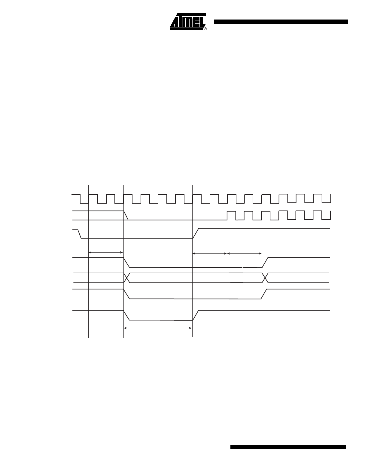
15.3.4.3 User Reset
The User Reset is entered when a low level is detected on the NRST pin and the bit URSTEN in
RSTC_MR is at 1. The NRST input signal is resynchronized with SLCK to insure proper behavior of the system.
The User Reset is entered as soon as a low level is detected on NRST. The Processor Reset
and the Peripheral Reset are asserted.
The User Reset is left when NRST rises, after a two-cycle resynchronization time and a Y-cycle
processor startup. The processor clock is re-enabled as soon as NRST is confirmed high.
When the processor reset signal is released, the RSTTYP field of the Status Register
(RSTC_SR) is loaded with the value 0x4, indicating a User Reset.
The NRST Manager guarantees that the NRST line is asserted for
EXTERNAL_RESET_LENGTH Slow Clock cycles, as programmed in the field ERSTL. However, if NRST does not rise after EXTERNAL_RESET_LENGTH because it is driven low
externally, the internal reset lines remain asserted until NRST actually rises.
Figure 15-6. User Reset State
SLCK
MCK
NRST
proc_nreset
RSTTYP
periph_nreset
NRST
(nrst_out)
Any
Freq.
Resynch.
2 cycles
Any XXX
>= EXTERNAL RESET LENGTH
Resynch.
2 cycles
Processor Startup
= 2 cycles
0x4 = User Reset
90
AT91CAP9S500A/AT91CAP9S250A
6264A–CAP–21-May-07
Page 91

15.3.4.4 Software Reset
The Reset Controller offers several commands used to assert the different reset signals. These
commands are performed by writing the Control Register (RSTC_CR) with the following bits at
1:
The software reset is entered if at least one of these bits is set by the software. All these commands can be performed independently or simultaneously. The software reset lasts Y Slow
Clock cycles.
The internal reset signals are asserted as soon as the register write is performed. This is
detected on the Master Clock (MCK). They are released when the software reset is left, i.e.; synchronously to SLCK.
If EXTRST is set, the nrst_out signal is asserted depending on the programming of the field
ERSTL. However, the resulting falling edge on NRST does not lead to a User Reset.
AT91CAP9S500A/AT91CAP9S250A
• PROCRST: Writing PROCRST at 1 resets the processor and the watchdog timer.
• PERRST: Writing PERRST at 1 resets all the embedded peripherals, including the memory
system, and, in particular, the Remap Command. The Peripheral Reset is generally used for
debug purposes.
• EXTRST: Writing EXTRST at 1 asserts low the NRST pin during a time defined by the field
ERSTL in the Mode Register (RSTC_MR).
If and only if the PROCRST bit is set, the Reset Controller reports the software status in the field
RSTTYP of the Status Register (RSTC_SR). Other Software Resets are not reported in
RSTTYP.
As soon as a software operation is detected, the bit SRCMP (Software Reset Command in
Progress) is set in the Status Register (RSTC_SR). It is cleared as soon as the software reset is
left. No other software reset can be performed while the SRCMP bit is set, and writing any value
in RSTC_CR has no effect.
6264A–CAP–21-May-07
91
Page 92

Figure 15-7. Software Reset
SLCK
MCK
Write RSTC_CR
proc_nreset
if PROCRST=1
RSTTYP
periph_nreset
if PERRST=1
NRST
(nrst_out)
if EXTRST=1
SRCMP in RSTC_SR
Any
Freq.
Any
Resynch.
1 cycle
Processor Startup
= 2 cycles
XXX
0x3 = Software Reset
EXTERNAL RESET LENGTH
8 cycles (ERSTL=2)
92
AT91CAP9S500A/AT91CAP9S250A
6264A–CAP–21-May-07
Page 93

15.3.4.5 Watchdog Reset
The Watchdog Reset is entered when a watchdog fault occurs. This state lasts Y Slow Clock
cycles.
When in Watchdog Reset, assertion of the reset signals depends on the WDRPROC bit in
WDT_MR:
• If WDRPROC is 0, the Processor Reset and the Peripheral Reset are asserted. The NRST
• If WDRPROC = 1, only the processor reset is asserted.
The Watchdog Timer is reset by the proc_nreset signal. As the watchdog fault always causes a
processor reset if WDRSTEN is set, the Watchdog Timer is always reset after a Watchdog
Reset, and the Watchdog is enabled by default and with a period set to a maximum.
When the WDRSTEN in WDT_MR bit is reset, the watchdog fault has no impact on the reset
controller.
Figure 15-8. Watchdog Reset
AT91CAP9S500A/AT91CAP9S250A
line is also asserted, depending on the programming of the field ERSTL. However, the
resulting low level on NRST does not result in a User Reset state.
SLCK
MCK
wd_fault
proc_nreset
RSTTYP
periph_nreset
Only if
WDRPROC = 0
NRST
(nrst_out)
15.3.5 Reset State Priorities
The Reset State Manager manages the following priorities between the different reset sources,
given in descending order:
Any
Freq.
Any
Processor Startup
= 2 cycles
XXX
0x2 = Watchdog Reset
EXTERNAL RESET LENGTH
8 cycles (ERSTL=2)
6264A–CAP–21-May-07
• Backup Reset
• Wake-up Reset
• Watchdog Reset
• Software Reset
• User Reset
Particular cases are listed below:
93
Page 94

• When in User Reset:
– A watchdog event is impossible because the Watchdog Timer is being reset by the
proc_nreset signal.
– A software reset is impossible, since the processor reset is being activated.
• When in Software Reset:
– A watchdog event has priority over the current state.
– The NRST has no effect.
• When in Watchdog Reset:
– The processor reset is active and so a Software Reset cannot be programmed.
– A User Reset cannot be entered.
15.3.6 Reset Controller Status Register
The Reset Controller status register (RSTC_SR) provides several status fields:
• RSTTYP field: This field gives the type of the last reset, as explained in previous sections.
• SRCMP bit: This field indicates that a Software Reset Command is in progress and that no
further software reset should be performed until the end of the current one. This bit is
automatically cleared at the end of the current software reset.
• NRSTL bit: The NRSTL bit of the Status Register gives the level of the NRST pin sampled on
each MCK rising edge.
• URSTS bit: A high-to-low transition of the NRST pin sets the URSTS bit of the RSTC_SR
register. This transition is also detected on the Master Clock (MCK) rising edge (see Figure
15-9). If the User Reset is disabled (URSTEN = 0) and if the interruption is enabled by the
URSTIEN bit in the RSTC_MR register, the URSTS bit triggers an interrupt. Reading the
RSTC_SR status register resets the URSTS bit and clears the interrupt.
Figure 15-9. Reset Controller Status and Interrupt
MCK
Peripheral Access
2 cycle
resynchronization
NRST
NRSTL
URSTS
rstc_irq
if (URSTEN = 0) and
(URSTIEN = 1)
read
RSTC_SR
2 cycle
resynchronization
94
AT91CAP9S500A/AT91CAP9S250A
6264A–CAP–21-May-07
Page 95

AT91CAP9S500A/AT91CAP9S250A
15.4 Reset Controller (RSTC) User Interface
Table 15-1. Reset Controller (RSTC) Register Mapping
Back-up Reset
Offset Register Name Access Reset Value
0x00 Control Register RSTC_CR Write-only -
0x04 Status Register RSTC_SR Read-only 0x0000_0001 0x0000_0000
0x08 Mode Register RSTC_MR Read/Write - 0x0000_0000
Note: 1. The reset value of RSTC_SR either reports a General Reset or a Wake-up Reset depending on last rising power supply.
Value
6264A–CAP–21-May-07
95
Page 96

15.4.1 Reset Controller Control Register Register Name: RSTC_CR
Access Type: Write-only
31 30 29 28 27 26 25 24
KEY
23 22 21 20 19 18 17 16
––––––––
15 14 13 12 11 10 9 8
–––––– –
76543210
––––EXTRSTPERRST–PROCRST
• PROCRST: Processor Reset
0 = No effect.
1 = If KEY is correct, resets the processor.
• PERRST: Peripheral Reset
0 = No effect.
1 = If KEY is correct, resets the peripherals.
• EXTRST: External Reset
0 = No effect.
1 = If KEY is correct, asserts the NRST pin.
•KEY: Password
Should be written at value 0xA5. Writing any other value in this field aborts the write operation.
96
AT91CAP9S500A/AT91CAP9S250A
6264A–CAP–21-May-07
Page 97

AT91CAP9S500A/AT91CAP9S250A
15.4.2 Reset Controller Status Register Register Name: RSTC_SR
Access Type: Read-only
31 30 29 28 27 26 25 24
––––––––
23 22 21 20 19 18 17 16
––––––SRCMPNRSTL
15 14 13 12 11 10 9 8
––––– RSTTYP
76543210
–––––––URSTS
• URSTS: User Reset Status
0 = No high-to-low edge on NRST happened since the last read of RSTC_SR.
1 = At least one high-to-low transition of NRST has been detected since the last read of RSTC_SR.
• RSTTYP: Reset Type
Reports the cause of the last processor reset. Reading this RSTC_SR does not reset this field.
RSTTYP Reset Type Comments
0 0 0 General Reset Both VDDCORE and VDDBU rising
0 0 1 Wake Up Reset VDDCORE rising
0 1 0 Watchdog Reset Watchdog fault occurred
0 1 1 Software Reset Processor reset required by the software
1 0 0 User Reset NRST pin detected low
• NRSTL: NRST Pin Level
Registers the NRST Pin Level at Master Clock (MCK).
• SRCMP: Software Reset Command in Progress
0 = No software command is being performed by the reset controller. The reset controller is ready for a software command.
1 = A software reset command is being performed by the reset controller. The reset controller is busy.
6264A–CAP–21-May-07
97
Page 98

15.4.3 Reset Controller Mode Register Register Name: RSTC_MR
Access Type: Read/Write
31 30 29 28 27 26 25 24
KEY
23 22 21 20 19 18 17 16
–––––––
15 14 13 12 11 10 9 8
–––– ERSTL
76543210
– – URSTIEN – – – URSTEN
• URSTEN: User Reset Enable
0 = The detection of a low level on the pin NRST does not generate a User Reset.
1 = The detection of a low level on the pin NRST triggers a User Reset.
• URSTIEN: User Reset Interrupt Enable
0 = USRTS bit in RSTC_SR at 1 has no effect on rstc_irq.
1 = USRTS bit in RSTC_SR at 1 asserts rstc_irq if URSTEN = 0.
• ERSTL: External Reset Length
This field defines the external reset length. The external reset is asserted during a time of 2
(ERSTL+1)
allows assertion duration to be programmed between 60 µs and 2 seconds.
•KEY: Password
Should be written at value 0xA5. Writing any other value in this field aborts the write operation.
Slow Clock cycles. This
98
AT91CAP9S500A/AT91CAP9S250A
6264A–CAP–21-May-07
Page 99

16. Real-time Timer (RTT)
16.1 Overview
The Real-time Timer is built around a 32-bit counter and used to count elapsed seconds. It
generates a periodic interrupt and/or triggers an alarm on a programmed value.
16.2 Block Diagram
Figure 16-1. Real-time Timer
AT91CAP9S500A/AT91CAP9S250A
SLCK
RTT_MR
RTTRST
reload
16-bit
Divider
RTT_MR
RTPRES
RTT_MR
RTTRST
RTT_VR
RTT_AR
0
10
32-bit
Counter
CRTV
ALMV
RTT_SR
RTT_SR
RTT_SR
=
read
set
RTTINC
reset
reset
set
RTT_MR
RTTINCIEN
rtt_int
RTT_MR
ALMIEN
ALMS
rtt_alarm
16.3 Functional Description
The Real-time Timer is used to count elapsed seconds. It is built around a 32-bit counter fed
by Slow Clock divided by a programmable 16-bit value. The value can be programmed in the
field RTPRES of the Real-time Mode Register (RTT_MR).
Programming RTPRES at 0x00008000 corresponds to feeding the real-time counter with a 1
Hz signal (if the Slow Clock is 32.768 Hz). The 32-bit counter can count up to 2
corresponding to more than 136 years, then roll over to 0.
The Real-time Timer can also be used as a free-running timer with a lower time-base. The
best accuracy is achieved by writing RTPRES to 3. Programming RTPRES to 1 or 2 is possible, but may result in losing status events because the status register is cleared two Slow
Clock cycles after read. Thus if the RTT is configured to trigger an interrupt, the interrupt
occurs during 2 Slow Clock cycles after reading RTT_SR. To prevent several executions of
the interrupt handler, the interrupt must be disabled in the interrupt handler and re-enabled
when the status register is clear.
6264A–CAP–21-May-07
32
seconds,
99
Page 100

The Real-time Timer value (CRTV) can be read at any time in the register RTT_VR (Real-time
Value Register). As this value can be updated asynchronously from the Master Clock, it is
advisable to read this register twice at the same value to improve accuracy of the returned
value.
The current value of the counter is compared with the value written in the alarm register
RTT_AR (Real-time Alarm Register). If the counter value matches the alarm, the bit ALMS in
RTT_SR is set. The alarm register is set to its maximum value, corresponding to
0xFFFF_FFFF, after a reset.
The bit RTTINC in RTT_SR is set each time the Real-time Timer counter is incremented. This
bit can be used to start a periodic interrupt, the period being one second when the RTPRES is
programmed with 0x8000 and Slow Clock equal to 32.768 Hz.
Reading the RTT_SR status register resets the RTTINC and ALMS fields.
Writing the bit RTTRST in RTT_MR immediately reloads and restarts the clock divider with the
new programmed value. This also resets the 32-bit counter.
Note: Because of the asynchronism between the Slow Clock (SCLK) and the System Clock (MCK):
1) The restart of the counter and the reset of the RTT_VR current value register is effective only
2 slow clock cycles after the write of the RTTRST bit in the RTT_MR register.
2) The status register flags reset is taken into account only 2 slow clock cycles after the read of
the RTT_SR (Status Register).
Figure 16-2. RTT Counting
MCK
RTPRES - 1
Prescaler
RTT
RTTINC (RTT_SR)
ALMS (RTT_SR)
APB Interface
APB cycle
0
...
ALMVALMV-10 ALMV+1
read RTT_SR
ALMV+2 ALMV+3
APB cycle
100
AT91CAP9S500A/AT91CAP9S250A
6264A–CAP–21-May-07
 Loading...