

Page 1
Features
General
• High-performance, Low-power secureAVR
• Low Power Idle and Power-Down Modes
• Bond Pad Locations Conforming to ISO 7816-2
• ESD Protection up to ± 4000V
• Operating Range: 2.7V to 5.5V
• Operating Temperature: -25°C to +85°C
• Internal Variable Frequency Oscillator up to 30 Mhz
• Available in Wafers, Modules and standard ROHS packages: SOIC8 or DFN8
TM
Enhanced RISC Architecture
Memory
• 96K bytes of ROM Program Memory
• 4K bytes of EEPROM including 128 OTP bytes and 384 bytes of Bit-addressable Area
– 1 to 64-byte Program/Erase
– 2 ms Program / 2 ms Erase
– Typically More than 500,000 Write/Erase Cycles at a Temperature of 25°C
– 10 Years Data Retention
• 2K bytes of RAM Memory
Peripherals
• ISO 7816 Controller
– Up to 625 kbps at 5 MHz
– Compliant with T = 0 and T = 1 Protocols
• High Speed Master/Slave SPI Serial Interface
– Supports clock up to 20MHz in Slave and Master Mode in typical conditions
– Double Buffering for high performance (16x2 bytes DPRAM buffers)
– DMA Controller for fast transfers between internal DPRAM to RAM
• Hardware Communication Interface Detection
• Two I/O Ports (supporting ISO 7816)
• Programmable Internal Oscillator (Up to 30 MHz for CPU)
• Two 16-bit Timers
• Random Number Generator (RNG)
• 2-level Interrupt Controller
• Hardware DES and Triple DES Engine DPA/DEMA Resistant
• Checksum Accelerator
• Code Signature Module
• CRC 16 & 32 Engine (Compliant with ISO/IEC 3309)
Secure
Microcontroller
for Security
Modules
AT90SO4
Summary
Security
• Dedicated Hardware for Protection Against SPA/DPA/SEMA/DEMA Attacks
• Advanced Protection Against Physical Attack, Including Active Shield
• Environmental Protection Systems (Voltage, Frequency, Temperature, Light
monitors...)
• Secure Memory Management/Access Protection (Supervisor Mode)
Development Tools
• Voyager Emulation Platform (ATV4 Plus) to Support Software Development
• IAR Systems EWAVR
• Software Libraries and Application Notes
®
V5.11B Debugger or Above
Note: This is a summary document. A complete document will be
available under NDA. For more information, please contact your
local Atmel sales office.
6579A–SMS–29Jan10
Page 2

Part Number
AT90SO4-xxx-P
AT: Atmel
90 : AVR Core
SO : Smart Object
4 : EEPROM Size
xxx : Chip Personalization Number*
P = Z : DFN8 Package
R : SOIC8 Package
* For more details about the Chip Personalization Number, please contact your local ATMEL sales office.
Description
Targeted for low cost security applications, the AT90SO4 is based on the secureAVR architecture that allows the linear addressing of up
to 8M bytes of code and up to 16M bytes of data as well as a number of new functional and security features. It is a low-power, high-performance, 8/16-bit microcontroller with ROM program memory, EEPROM data memory based on the secureAVR enhanced RISC
architecture. By executing powerful instructions in a single clock cycle, the AT90SO4 achieves throughputs close to 1 MIPS per MHz. Its
Harvard architecture includes 32 general purpose working registers directly connected to the ALU, allowing two independent registers to
be accessed in one single instruction executed in one clock cycle.
The ability to map the EEPROM in the code space allows parts of the program memory to be reprogrammed in-system. This technology
combined with the versatile 8/16-bit CPU on a monolithic chip provides a highly flexible and cost-effective solution to many embedded
security applications.
Additional security features include power and frequency protection logic, logical scrambling on program data and addresses, Power
Analysis countermeasures and memory accesses controlled by a supervisor mode. A block diagram of the AT90SO4 is shown in Figure
1 hereafter.
High-Speed SPI Controller
The AT90SO4 hosts a High Speed SPI interface for full-duplex and synchronous data transfer. When configured as a master, the controller provides clock up to 20MHz thanks to the dedicated internal VFO clock system.
A specific DMA contoller allows fast tranfers between DPRAM banks to CPU RAM. The internal DPRAM memory provides 4 DPRAM
buffers of 16 bytes each: 2 for Reception and 2 for Transmission.
The SPI controller features three sources of interrupt (Byte Transmitted, Time-out and Reception Overflow) and a programmable clock
and inter-bytes (guardtime) delays.
2
AT90SO4
6579A–SMS–29Jan10
Page 3
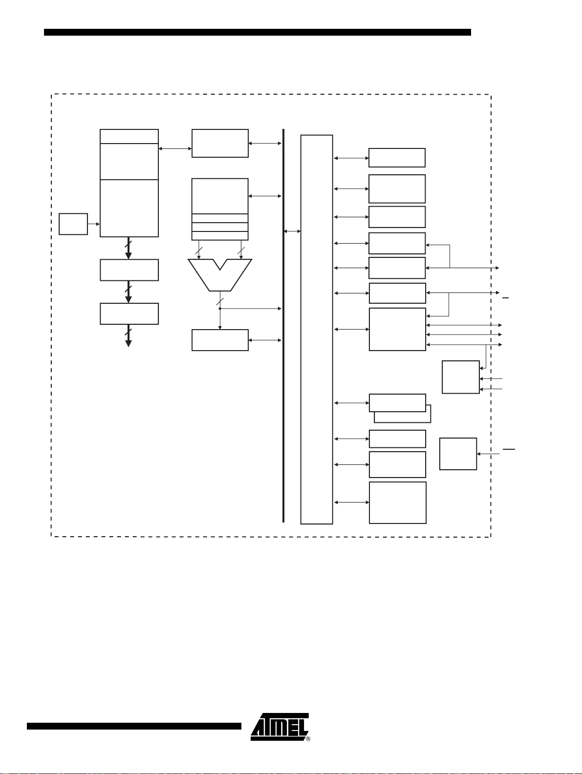
Figure 1. AT90SO4 secureAVR Enhanced RISC Architecture
Instruction
Decoder
Program
Memory
Instruction
Register
Access
Control
General
Purpose
Registers
X
Y
Z
Status
Register
RAM
Data Memory
Interrupt
Unit
ISO 7816
I/O Port 0
Control
Lines
ALU
EEPROM
User Memory
OTP
PC
Secure
Control
VCC
GND
Access
Control
IN/OUT0
Data Bus
8-bit
RNG
16
16
16
8
88
DES
DPA Counter
measures
Reset
Circuit
RST
ISO 7816
Controller
CRC and
Checksum
Accelerator
Timer 1
Timer 0
ISO7816
I/O Port 1
SPI
Controller
SPI_MISO
SPICLK /
ISOCLK
SPI_MOSI
IN/OUT1 /
SS
AT90SO4
6579A–SMS–29Jan10
3
Page 4
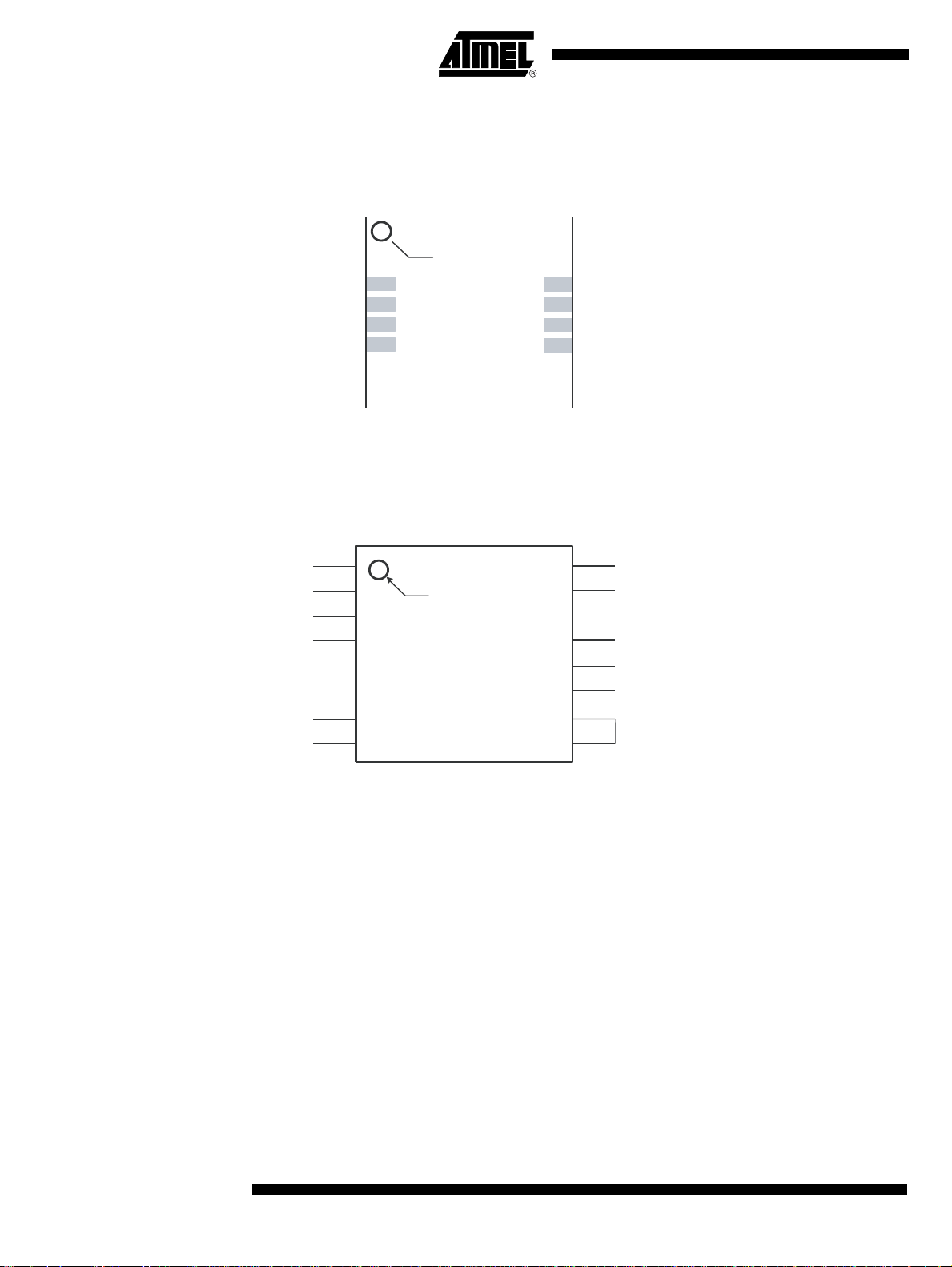
Pinout and Package Information
2
3
1
4
8
7
6
5
SPI_MISO
VCC
RST
SPI_CLK / ISO_CLK
SPI_MOSI
GND
SPI_SS / IO1
IO0
AT90SO4
DFN8
INDEX CORNER
AT90SO4
SOIC8
INDEX CORNER
SPI_MOSI
GND
I01 / SPI_SS
IO0
1
2
3
4
8
7
6
5
SPI_MISO
VCC
RST
ISO_CLK / SPI_SCK
Figure 2. Pinout AT90SO4 - Package DFN8
Figure 3. Pinout AT90SO4 - Package SOIC8
4
AT90SO4
6579A–SMS–29Jan10
Page 5

Figure 4. Dual Fleat No Lead Package, 8 leads
AT90SO4
6579A–SMS–29Jan10
5
Page 6

Figure 5. Plastic Small Outline Package - 8-lead - 0.209” Body
COMMON DIMENSIONS
(Unit of Measure = mm)
SYMBOL
MIN
NOM
MAX
NOTE
Notes: 1. This drawing is for general information only; refer to EIAJ Drawing EDR-7320 for additional information.
2. Mismatch of the upper and lower dies and resin burrs are not included.
3. It is recommended that upper and lower cavities be equal. If they are different, the larger dimension shall be regarded.
4. Determines the true geometric position.
5. Values b and C apply to pb/Sn solder plated terminal.
The standard thickness of the solder layer shall be 0.010 +0.010/-0.005 mm.
A 1.70 2.16
A1 0.05 0.25
b 0.35 0.48 5
C 0.15 0.35 5
D 5.13 5.35
E1 5.18 5.40 2, 3
E 7.70 8.26
L 0.51 0.85
?
0˚ 8˚
e 1.27 BSC 4
End View
Side View
e
b
A
A1
D
E
N
1
C
E1
?
L
Top View
6
AT90SO4
6579A–SMS–29Jan10
Page 7

Product Marking
39WWzzz
LLLLL
YYMM
39: Chip Identification Number
WW: ROM Code
zzz: Chip Personalization Number
LLLLL : Lot Number
YYMM : Date Code
39WWzzz
LLLLL
YYMM
39: Chip Identification Number
WW: ROM Code
zzz: Chip Personalization Number
LLLLL : Lot Number
YYMM : Date Code
Figure 1. Package DFN8
AT90SO4
Figure 1. Package SOIC8
6579A–SMS–29Jan10
7
Page 8

Product Characteristics
Maximum Ratings
Table 1. Absolute Maximum Ratings
Symbol Parameter Min. Max. Unit
V
V
T
E
EEPROM
CC
IN
A
Supply Voltage -0.3 7.5 V
Input Voltage VSS-0.3 VCC+0.3 V
Operating Temperature -25 +85 °C
EEPROM Endurance
for write/erase cycles
500 000
(1)
cycles
V
DataRetent ion
EEPROM Data Reten-
10 Year s
tion Virgin
ESD Electrostatic Dis-
4 kV
charge (HBM)
L
up
Latch-up +/- 200 mA
1. Depends on conditions. Please refer to “EEPROM Reliability & Qualification Specification”
(PE/SPEC/032).
AC/DC Characteristics (2.7V - 5.50V range; T= -2 5°C to +85°C)
Table 2. DC Characteristics (2.7V - 5.50V range; T= -25°C to +85°C)
Symbol Parameter Condition Min. Typ. Max. Units
V
Supply Voltage 2.7 5.50 V
CC
Supply Voltage
V
CC
Supply Voltage
Input High Voltage - I/O 0..1
Input High Voltage - ISOCLK
V
IH
Input High Voltage - RST
Input High Voltage - MISO, MOSI
Input Low Voltage - I/O 0..1
Input Low Voltage - ISOCLK
V
IL
Input Low Voltage - RST
Input Low Voltage - MISO, MOSI
Leakage High Current- I/O 0..1
Leakage High Current - ISOCLK
I
IH
Leakage High Current - RST
Leakage High Current - MISO, MOSI
Leakage Low Current - I/O 0..1
Leakage Low Current - ISOCLK
I
IL
Leakage Low Current - RST
Leakage Low Current - MISO, MOSI
5.0V (+/- 10%)
3.0V (+/- 10%)
5V, 3V
5V, 3V
5V, 3V, VIN = V
5V, 3V, VIN = V
4.5
2.7
0.7*V
0.7*V
0.7*V
0.7*Vcc
-0.3
-0.3
-0.3
-0.3
-10
IH
-10
-10
-10
-40
IL
-10
-40
-40
CC
CC
CC
5.0
3.0
5.5
3.3
VCC+0.3
+0.3
V
CC
V
+0.3
CC
+0.3
V
CC
0.2*V
CC
0.2*V
CC
0.2*V
CC
0.2*V
CC
10
10
10
10
10
10
10
10
μA
μA
V
V
V
8
AT90SO4
6579A–SMS–29Jan10
Page 9

Table 2. DC Characteristics (2.7V - 5.50V range; T= -25°C to +85°C)
Symbol Parameter Condition Min. Typ. Max. Units
AT90SO4
Output Low Voltage - I/O 0..1
V
OL
Output Low Voltage - MISO, MOSI
Output High Voltage - I/O 0..1
V
OH
Output High Voltage - MISO, MOSI
Pin Pull-up I/O0, RST, I/O1, MISO,
R
I/O
MOSI
5V, IOL = 1mA
3V, IOL = 1mA
5V, 3V, IOH = 1mA
0
0
0.7*Vcc
0.7*Vcc
0.08*V
0.15*V
Vcc
Vcc
CC
CC
V
V
220 KOhm
Table 3. AC Characteristics (2.7V - 5.50V range; T= -25°C to +85°C)
Symbol Parameter Condition Min. Typ. Max. Units
f
External Clock Frequency 1 5 MHz
CLK
f
VFO
f
VFO
Average
t
EEPROM
Variable Frequency Oscillator
Average Variable Frequency
Oscillator
(2)
EEPROM Write Time (erase+write) 1.6 2 2.4 ms
(1)
TrI/O Output Rise Time (HRD Mode)
TfI/O Output Fall Time
1. Please refer to Application Note “How to estimate a performance of a running code “ TPR0231X for the
dependence on temperature, clock jitter and clock dividers.
Expected value at 25°C
Clock Jitter not enabled
5V, 3V
Expected value at 25°C
Clock Jitter enabled
5V, 3V
C
=30pF
out
R
=20kOhm
pullup
C
=30pF
out
R
=20kOhm
pullup
28 31 34 MHz
28 MHz
100 ns
100 ns
Table 4. Security Characteristics (2.7V - 5.50V range; T= -25°C to +85°C)
Symbol Parameter Condition Min. Typ. Max. Units
V
V
T
Max
T
Voltage Monitor: High Level
MAX
Detection
Voltage Monitor: Low Level
MIN
Detection
External Frequency Monitor:
f
MAX
High Level Detection
External Frequency Monitor: Low
f
MIN
Level Detection
Temperature Monitor: High Level
MON
Detection
Temperature Monitor: Low Level
MON
Detection
Min
Chip trimmed to operate at 5V,
3V
Duty cycle = 40% to 60%
Running on External Clock
Duty cycle = 40% to 60%
Running on External Clock
5.5 V
2.7
5 MHz
1 MHz
85 °C
-25 °C
V
6579A–SMS–29Jan10
9
Page 10

Table 5. Icc Characteristics (2.7V - 5.50V range; T= -25°C to +85°C)
Symbol Parameter Condition Min. Typ. Max. Units
I
cc Run Mode
I
cc Run Mode
Supply Current in Run Mode
f
=5MHz
CLK
Supply Current in Run Mode
f
=30MHz
VFO
5V, 3V
From ROM
5V, 3V
From ROM
6 mA
10 mA
Supply Current add-on when DES is
I
cc DES
running
f
=5MHz
CLK
5V, 3V 4 mA
Supply Current add-on when DES is
I
cc DES
I
cc IDLE
running
f
=30MHz
VFO
Supply Current in IDLE Mode
Clock :5MHz
5V, 3V 10 mA
5V, 3V 2 mA
Supply Current in POWER-DOWN
I
cc POWER-DOWN
Mode
5V, 3V 200 μA
Clock : 1MHz
Supply Current in POWER-DOWN
I
cc POWER-DOWN
Mode
5V, 3V 200 μA
No Clock Running
Table 6. High Speed SPI characteristics in Master Mode (2.7V - 5.50V range; T= -25°C to +85°C)
Symbol Parameter Condition Min. Typ. Max. Units
t
MISOsetup
t
MISOhold
t
SCKrising
t’
MISOsetup
t’
MISOhold
t
SCKfalling
SCK
MISO Setup time before SCK rises
MISO Hold time after SCK rises
SCK rising to MOSI Delay
MISO Setup time before SCK falls
MISO Hold time after SCK falls
SCK falling to MOSI Delay
Host frequency
C
=10pF
OUT
=20pF
C
OUT
C
=10pF
OUT
=20pF
C
OUT
C
=10pF
OUT
C
=20pF
OUT
C
=10pF
OUT
=20pF
C
OUT
C
=10pF
OUT
=20pF
C
OUT
C
=10pF
OUT
C
=20pF
OUT
C
=10pF
OUT
=20pF
C
OUT
10 ns
10 ns
10 ns
10 ns
10 ns
10 ns
20 MHz
10
AT90SO4
6579A–SMS–29Jan10
Page 11

Table 7. High Speed SPI characteristics in Slave Mode (2.7V - 5.50V range; T= -25°C to +85°C)
Symbol Parameter Condition Min. Typ. Max. Units
C
=10pF
t
SCKfalling
t
SCKrising
t
MOSIsetup
t
MOSIhold
t’
MOSIsetup
t’
MOSIhold
t
SSsetup
t
dat->dat
SCK
SCK falling to MISO Delay
SCK rising to MISO Delay
MOSI Setup time before SCK rises
MOSI Hold time after SCK rises
MOSI Setup time before SCK falls
MOSI Hold time after SCK falls
SS Setup time
Interbyte delay
Slave frequency
C
C
C
C
C
C
C
C
C
C
C
C
C
C
C
C
C
OUT
OUT
OUT
OUT
OUT
OUT
OUT
OUT
OUT
OUT
OUT
OUT
OUT
OUT
OUT
OUT
OUT
OUT
=20pF
=10pF
=20pF
=10pF
=20pF
=10pF
=20pF
=10pF
=20pF
=10pF
=20pF
=10pF
=20pF
=10pF
=20pF
=10pF
=20pF
13 ns
13 ns
10 ns
10 ns
10 ns
10 ns
10 ns
10 ns
20 MHz
AT90SO4
6579A–SMS–29Jan10
11
Page 12

12
AT90SO4
6579A–SMS–29Jan10
Page 13

6579A–SMS–29Jan10
© Atmel Corporation 2010. All rights reserved. Atmel
®
, logo and combinations thereof, Everywhere You Are® and others, are registered
trademarks or trademarks of Atmel Corporation or its subsidiaries. Other terms and product names may be trademarks of others.
Disclaimer: The information in this document is provided in connection with Atmel products. No license, express or implied, by estoppel or otherwise, to any
intellectual property right is granted by this document or in connection with the sale of Atmel products. EXCEPT AS SET FORTH IN ATMEL’S TERMS AND CONDI-
TIONS OF SALE LOCATED ON ATMEL’S WEB SITE, ATMEL ASSUMES NO LIABILITY WHATSOEVER AND DISCLAIMS ANY EXPRESS, IMPLIED OR STATUTORY
WARRANTY RELATING TO ITS PRODUCTS INCLUDING, BUT NOT LIMITED TO, THE IMPLIED WARRANTY OF MERCHANTABILITY, FITNESS F OR A PARTICULAR
PURPOSE, OR NON-INFRINGEMENT. IN NO EVENT SHALL ATMEL BE LIABLE FOR ANY DIRECT, INDIRECT, CONSEQUENTIAL, PUNITIVE, SPECIAL OR INCIDENTAL DAMAGES (INCLUDING, WITHOUT LIMITATION, DAMAGES FOR LOSS OF PROFITS, BUSINESS INTERRUPTION, OR LOSS OF INFORMATION) ARISING OUT
OF THE USE OR INABILITY TO USE THIS DOCUMENT, EVEN IF ATMEL HAS BEEN ADVISED OF THE POSSIBILITY OF SUCH DAMAGES. Atmel makes no
representations or warranties with respect to the accuracy or completeness of the contents of this document and reserves the right to make changes to specifications
and product descriptions at any time without notice. Atmel does not make any commitment to update the information contained herein. Atmel’s products are not
intended, authorized, or warranted for use as components in applications intended to support or sustain life.
Atmel Corporation Atmel Operations
2325 Orchard Parkway
San Jose, CA 95131, USA
Tel: 1(408) 441-0311
Fax: 1(408) 487-2600
Regional Headquarters
Europe
Atmel Sarl
Route des Arsenaux 41
Case Postale 80
CH-1705 Fribourg
Switzerland
Tel: (41) 26-426-5555
Fax: (41) 26-426-5500
Asia
Room 1219
Chinachem Golden Plaza
77 Mody Road Tsimshatsui
East Kowloon
Hong Kong
Tel: (852) 2721-9778
Fax: (852) 2722-1369
Japan
9F, Tonetsu Shinkawa Bldg.
1-24-8 Shinkawa
Chuo-ku, Tokyo 104-0033
Japan
Tel: (81) 3-3523-3551
Fax: (81) 3-3523-7581
Memory
2325 Orchard Parkway
San Jose, CA 95131, USA
Tel: 1(408) 441-0311
Fax: 1(408) 436-4314
Microcontrollers
2325 Orchard Parkway
San Jose, CA 95131, USA
Tel: 1(408) 441-0311
Fax: 1(408) 436-4314
La Chantrerie
BP 70602
44306 Nantes Cedex 3, France
Tel: (33) 2-40-18-18-18
Fax: (33) 2-40-18-19-60
ASIC/ASSP/Secure Microcontroller Solutions
Zone Industrielle
13106 Rousset Cedex, France
Tel: (33) 4-42-53-60-00
Fax: (33) 4-42-53-60-01
1150 East Cheyenne Mtn. Blvd.
Colorado Springs, CO 80906, USA
Tel: 1(719) 576-3300
Fax: 1(719) 540-1759
Scottish Enterprise Technology Park
Maxwell Building
East Kilbride G75 0QR, Scotland
Tel: (44) 1355-803-000
Fax: (44) 1355-242-743
RF/Automotive
Theresienstrasse 2
Postfach 3535
74025 Heilbronn, Germany
Tel: (49) 71-31-67-0
Fax: (49) 71-31-67-2340
1150 East Cheyenne Mtn. Blvd.
Colorado Springs, CO 80906, USA
Tel: 1(719) 576-3300
Fax: 1(719) 540-1759
Biometrics/Imaging/Hi-Rel MPU/
High Speed Converters/RF Datacom
Avenue de Rochepleine
BP 123
38521 Saint-Egreve Cedex, France
Tel: (33) 4-76-58-30-00
Fax: (33) 4-76-58-34-80
Literature Requests
www.atmel.com/literature
 Loading...