

Page 1

Features
• Utilizes the AVR
• AVR – High-performance and Low-power RISC Architecture
– 118 Powerful Instructions – Most Single Clock Cycle Execution
– 32x8GeneralPurposeWorkingRegisters
– Up to 10 MIPS Throughput at 10 MHz
• Data and Non-volatile Program Memory
– 2K Bytes of In-System Programmable Flash
Endurance 1,000 Write/Erase Cycles
– 128 Bytes of SRAM
– 128 Bytes of In-System Programmable EEPROM
Endurance: 100,000 Write/Erase Cycles
– Programming Lock for Flash Program and EEPROM Data Security
• Peripheral Features
– One 8-bit Timer/Counter with Separate Prescaler
– One 16-bit Timer/Counter with Separate Prescaler,
Compare, Capture Modes and 8-, 9-, or 10-bit PWM
– On-chip Analog Comparator
– Programmable Watchdog Timer with On-chip Oscillator
– SPI Serial Interface for In-System Programming
–FullDuplexUART
• • Special Microcontroller Features
– Low-power Idle and Power-down Modes
– External and Internal Interrupt Sources
• • Specifications
– Low-power, High-speed CMOS Process Technology
– Fully Static Operation
• Power Consumption at 4 MHz, 3V, 25°C
– Active: 2.8 mA
– Idle Mode: 0.8 mA
– Power-down Mode: <1 µA
• I/O and Packages
– 15 Programmable I/O Lines
– 20-pin PDIP and SOIC
• Operating Voltages
– 2.7 - 6.0V (AT90S2313-4)
– 4.0 - 6.0V (AT90S2313-10)
• Speed Grades
– 0 - 4 MHz (AT90S2313-4)
– 0 - 10 MHz (AT90S2313-10)
®
RISC Architecture
8-bit
Microcontroller
with 2K Bytes
of In-System
Programmable
Flash
AT90S2313
Pin Configuration
PDIP/SOIC
Rev. 0839I–AVR–06/02
1
Page 2
Description The AT90S2313 is a low-power CMOS 8-bit microcontroller based on the AVR RISC
architecture. By executing powerful instructions in a single clock cycle, the AT90S2313
achieves throughputs approaching 1 MIPS per MHz allowing the system designer to
optimize power consumption versus processing speed.
The AVR core combines a rich instruction set with 32 general purpose working registers.
All the 32 registers are directly connected to the Arithmetic Logic Unit (ALU), allowing
two independent registers to be accessed in one single instruction executed in one clock
cycle. The resulting architecture is more code efficient while achieving throughputs up to
ten times faster than conventional CISC microcontrollers.
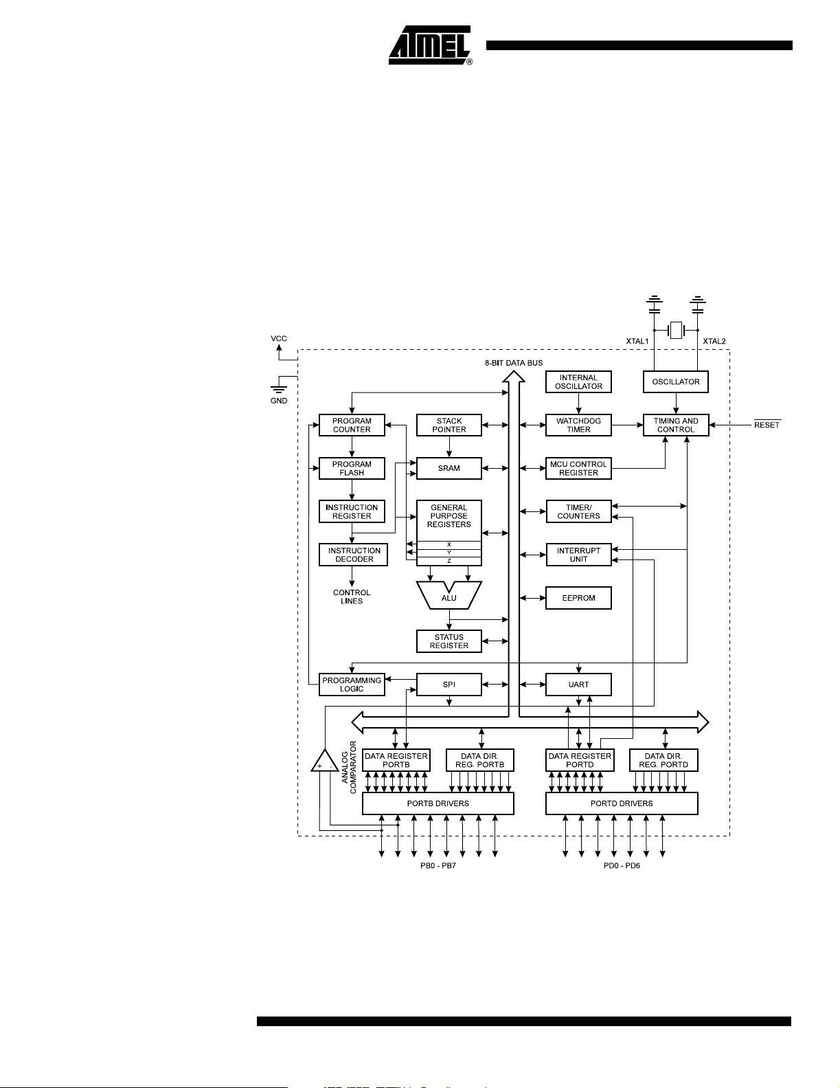
Figure 1. The AT90S2313 Block Diagram
The AT90S2313 provides the following features: 2K bytes of In-System Programmable
Flash, 128 bytes EEPROM, 128 bytes SRAM, 15 general purpose I/O lines, 32 general
purpose working registers, flexible Timer/Counters with compare modes, internal and
external interrupts, a programmable serial UART, programmable Watchdog Timer with
internal Oscillator, an SPI serial port for Flash memory downloading and two software
2
AT90S2313
0839I–AVR–06/02
Page 3

selectable power-saving modes. The Idle mode stops the CPU while allowing the
SRAM, Timer/Counters, SPI port and interrupt system to continue functioning. The
Power-down mode saves the register contents but freezes the Oscillator, disabling all
other chip functions until the next external interrupt or Hardware Reset.
The device is manufactured using Atmel’s high-density non-volatile memory technology.
The On-chip In-System Programmable Flash allows the Program memory to be reprogrammed in-system through an SPI serial interface or by a conventional non-volatile
memory programmer. By combining an enhanced RISC 8-bit CPU with In-System Programmable Flash on a monolithic chip, the Atmel AT90S2313 is a powerful
microcontroller that provides a highly flexible and cost-effective solution to many embedded control applications.
The AT90S2313 AVR is supported with a full suite of program and system development
tools including: C compilers, macro assemblers, program debugger/simulators, In-Circuit Emulators and evaluation kits.
Pin Descriptions
VCC Supply voltage pin.
GND Ground pin.
AT90S2313
Port B (PB7..PB0) Port B is an 8-bit bi-directional I/O port. Port pins can provide internal pull-up resistors
(selected for each bit). PB0 and PB1 also serve as the positive input (AIN0) and the
negative input (AIN1), respectively, of the On-chip Analog Comparator. The Port B output buffers can sink 20 mA and can drive LED displays directly. When pins PB0 to PB7
are used as inputs and are externally pulled low, they will source current if the internal
pull-up resistors are activated. The Port B pins are tri-stated when a reset condition
becomes active, even if the clock is not active.
Port B also serves the functions of various special features of the AT90S2313 as listed
on page 51.
Port D (PD6..PD0) Port D has seven bi-directional I/O ports with internal pull-up resistors, PD6..PD0. The
Port D output buffers can sink 20 mA. As inputs, Port D pins that are externally pulled
low will source current if the pull-up resistors are activated. The Port D pins are tri-stated
when a reset condition becomes active, even if the clock is not active.
Port D also serves the functions of various special features of the AT90S2313 as listed
on page 56.
RESET
XTAL1 Input to the inverting Oscillator amplifier and input to the internal clock operating circuit.
XTAL2 Output from the inverting Oscillator amplifier.
Reset input. A low level on this pin for more than 50 ns will generate a Reset, even if the
clock is not running. Shorter pulses are not guaranteed to generate a Reset.
0839I–AVR–06/02
3
Page 4
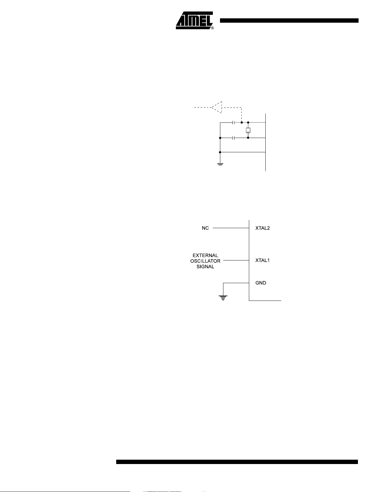
Crystal Oscillator XTAL1 and XTAL2 are input and output, respectively, of an inverting amplifier that can
be configured for use as an On-chip Oscillator, as shown in Figure 2. Either a quartz
crystal or a ceramic resonator may be used. To drive the device from an external clock
source, XTAL2 should be left unconnected while XTAL1 is driven, as shown in Figure 3.
Figure 2. Oscillator Connections
MAX 1 HC BUFFER
HC
C2
C1
Note: When using the MCU Oscillator as a clock for an external device, an HC buffer should be
connected as indicated in the figure.
XTAL2
XTAL1
GND
Figure 3. External Clock Drive Configuration
4
AT90S2313
0839I–AVR–06/02
Page 5
AT90S2313
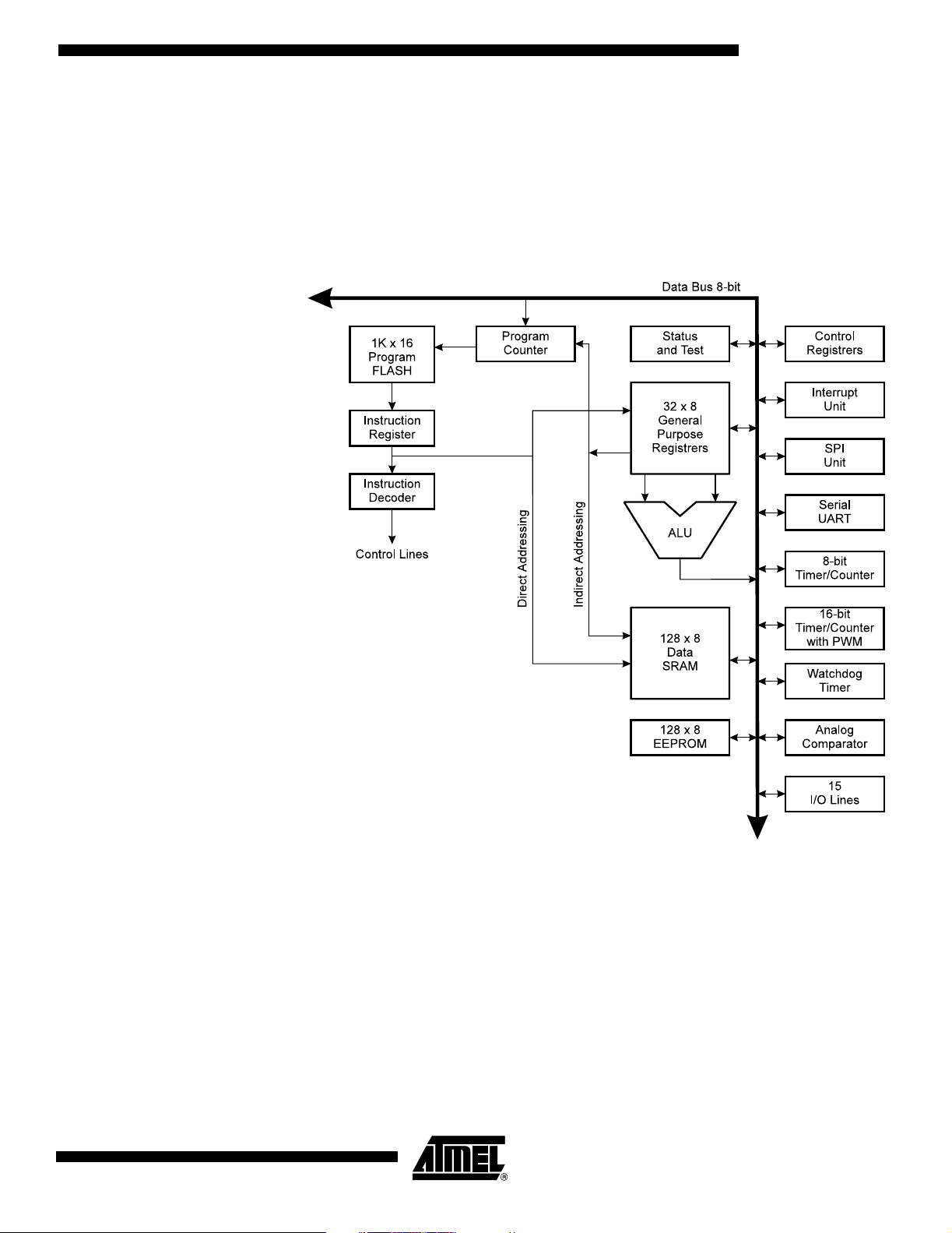
Architectural Overview
The fast-access Register File concept contains 32 x 8-bit general purpose working registers with a single clock cycle access time. This means that during one single clock
cycle, one ALU (Arithmetic Logic Unit) operation is executed. Two operands are output
from the Register File, the operation is executed, and the result is stored back in the
Register File – in one clock cycle.
Figure 4. The AT90S2313 AVR RISC Architecture
0839I–AVR–06/02
Six of the 32 registers can be used as three 16-bit indirect address register pointers for
Data Space addressing – enabling efficient address calculations. One of the three
address pointers is also used as the address pointer for the constant table look-up function. These added function registers are the 16-bit X-register, Y-register, and Z-register.
The ALU supports arithmetic and logic functions between registers or between a constant and a register. Single register operations are also executed in the ALU. Figure 4
shows the AT90S2313 AVR RISC microcontroller architecture.
In addition to the register operation, the conventional memory addressing modes can be
used on the Register File as well. This is enabled by the fact that the Register File is
assigned the 32 lowermost Data Space addresses ($00 - $1F), allowing them to be
accessed as though they were ordinary memory locations.
5
Page 6
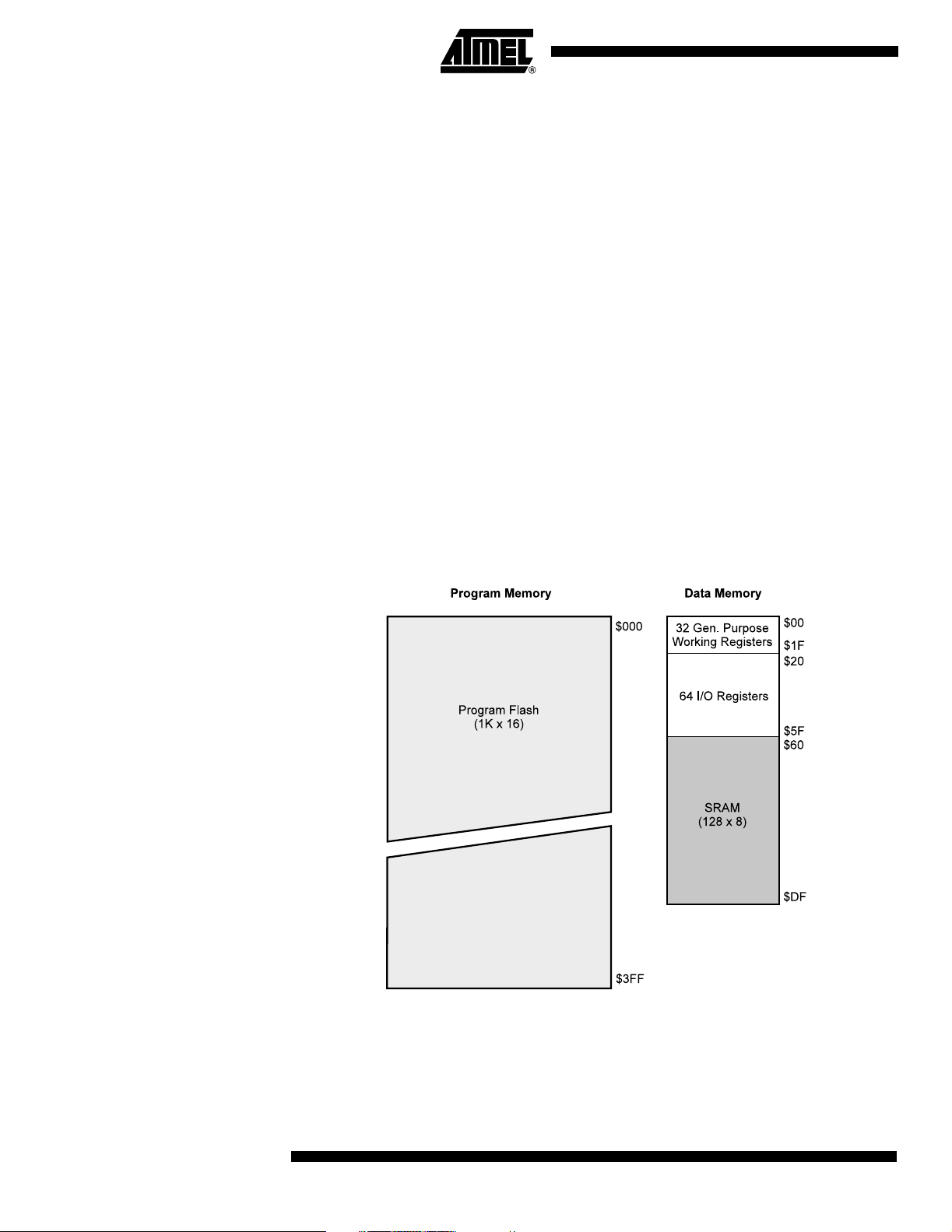
The I/O memory space contains 64 addresses for CPU peripheral functions such as
control registers, Timer/Counters, A/D converters and other I/O functions. The I/O memory can be accessed directly or as the Data Space locations following those of the
Register File, $20 - $5F.
The AVR has Harvard architecture – with separate memories and buses for program
and data. The program memory is accessed with a 2-stage pipeline. While one instruction is being executed, the next instruction is pre-fetched from the program memory.
This concept enables instructions to be executed in every clock cycle. The program
memory is In-System Programmable Flash memory.
With the relative jump and call instructions, the whole 1K address space is directly
accessed. Most AVR instructions have a single 16-bit word format. Every program
memory address contains a 16- or 32-bit instruction.
During interrupts and subroutine calls, the return address Program Counter (PC) is
stored on the Stack. The Stack is effectively allocated in the general data SRAM, and
consequently the stack size is only limited by the total SRAM size and the usage of the
SRAM. All user programs must initialize the SP in the reset routine (before subroutines
or interrupts are executed). The 8-bit Stack Pointer (SP) is read/write accessible in the
I/O space.
The 128 bytes data SRAM + Register File and I/O Registers can be easily accessed
through the five different addressing modes supported in the AVR architecture.
The memory spaces in the AVR architecture are all linear and regular memory maps.
Figure 5. Memory Maps
A flexible interrupt module has its control registers in the I/O space with an additional
Global Interrupt Enable bit in the Status Register. All the different interrupts have a separate Interrupt Vector in the Interrupt Vector table at the beginning of the program
memory. The different interrupts have priority in accordance with their Interrupt Vector
position. The lower the Interrupt Vector address, the higher the priority.
6
AT90S2313
0839I–AVR–06/02
Page 7
AT90S2313
General Purpose Register File
Figure 6 shows the structure of the 32 general purpose registers in the CPU.
Figure 6. AVR CPU General Purpose Working Registers
70Addr.
R0 $00
R1 $01
R2 $02
…
R13 $0D
General R14 $0E
Purpose R15 $0F
Working R16 $10
Registers R17 $11
…
R26 $1A X-register Low Byte
R27 $1B X-register High Byte
R28 $1C Y-register Low Byte
R29 $1D Y-register High Byte
R30 $1E Z-register Low Byte
R31 $1F Z-register High Byte
All the register operating instructions in the instruction set have direct and single-cycle
access to all registers. The only exception is the five constant arithmetic and logic
instructions SBCI, SUBI, CPI, ANDI, ORI between a constant and a register and the LDI
instruction for load immediate constant data. These instructions apply to the second half
of the registers in the Register File (R16..R31). The general SBC, SUB, CP, AND, OR,
and all other operations between two registers or on a single register apply to the entire
Register File.
X-register, Y-register, and Zregister
As shown in Figure 6, each register is also assigned a data memory address, mapping
them directly into the first 32 locations of the user Data Space. Although the Register
File is not physically implemented as SRAM locations, this memory organization provides great flexibility in access of the registers, as the X-, Y-, and Z-registers can be set
to index any register in the file.
The registers R26..R31 have some added functions to their general purpose usage.
These registers are the address pointers for indirect addressing of the Data Space. The
three indirect address registers X, Y and Z are defined in Figure 7.
Figure 7. X-, Y-, and Z-Registers
15 0
X-register 7 0 7 0
R27 ($1B) R26 ($1A)
15 0
Y-register 7 0 7 0
R29 ($1D) R28 ($1C)
15 0
Z-register 7 0 7 0
R31 ($1F) R30 ($1E)
0839I–AVR–06/02
7
Page 8

In the different addressing modes these address registers have functions as fixed displacement, automatic increment and decrement (see the descriptions for the different
instructions).
ALU – Arithmetic Logic Unit
In-SystemProgrammable Flash Program Memory
The high-performance AVR ALU operates in direct connection with all the 32 general
purpose working registers. Within a single clock cycle, ALU operations between registers in the Register File are executed. The ALU operations are divided into three main
categories – arithmetic, logical, and bit functions.
The AT90S2313 contains 2K bytes On-chip In-System Programmable Flash memory for
program storage. Since all instructions are 16- or 32-bit words, the Flash is organized as
1K x 16. The Flash memory has an endurance of at least 1,000 write/erase cycles.
The AT90S2313 Program Counter (PC) is 10 bits wide, thus addressing the 1,024 program memory addresses.
See page 60 for a detailed description on Flash data downloading. See page 10 for the
different addressing modes.
EEPROM Data Memory The AT90S2313 contains 128 bytes of EEPROM data memory. It is organized as a sep-
arate data space in which single bytes can be read and written. The EEPROM has an
endurance of at least 100,000 write/erase cycles. The access between the EEPROM
and the CPU is described on page 39, specifying the EEPROM Address Register, the
EEPROM Data Register and the EEPROM Control Register.
For the SPI data downloading, see page 68 for a detailed description.
8
AT90S2313
0839I–AVR–06/02
Page 9
SRAM Data Memory Figure 8 shows how the AT90S2313 data memory is organized.
Figure 8. SRAM Organization
Register File Data Address Space
R0 $00
R1 $01
R2 $02
……
R29 $1D
R30 $1E
R31 $1F
I/O Registers
$00 $20
$01 $21
$02 $22
……
$3D $5D
$3E $5E
$3F $5F
AT90S2313
Internal SRAM
$60
$61
$62
…
$DD
$DE
$DF
The 224 data memory locations address the Register File, I/O memory and the data
SRAM. The first 96 locations address the Register File + I/O memory, and the next 128
locations address the data SRAM.
The five different addressing modes for the data memory cover: Direct, Indirect with Displacement, Indirect, Indirect with Pre-decrement and Indirect with Post-increment. In the
Register File, registers R26 to R31 feature the indirect addressing pointer registers.
The Direct addressing reaches the entire data address space.
The Indirect with Displacement mode features 63 address locations reached from the
base address given by the Y- and Z-registers.
When using register indirect addressing modes with automatic pre-decrement and postincrement, the address registers X, Y, and Z are used and decremented and
incremented.
The 32 general purpose working registers, 64 I/O Registers and the 128 bytes of data
SRAM in the AT90S2313 are all directly accessible through all these addressing modes.
0839I–AVR–06/02
9
Page 10
Program and Data Addressing Modes
The AT90S2313 AVR RISC microcontroller supports powerful and efficient addressing
modes for access to the Program memory (Flash) and Data memory. This section
describes the different addressing modes supported by the AVR architecture. In the figures, OP means the operation code part of the instruction word. To simplify, not all
figures show the exact location of the addressing bits.
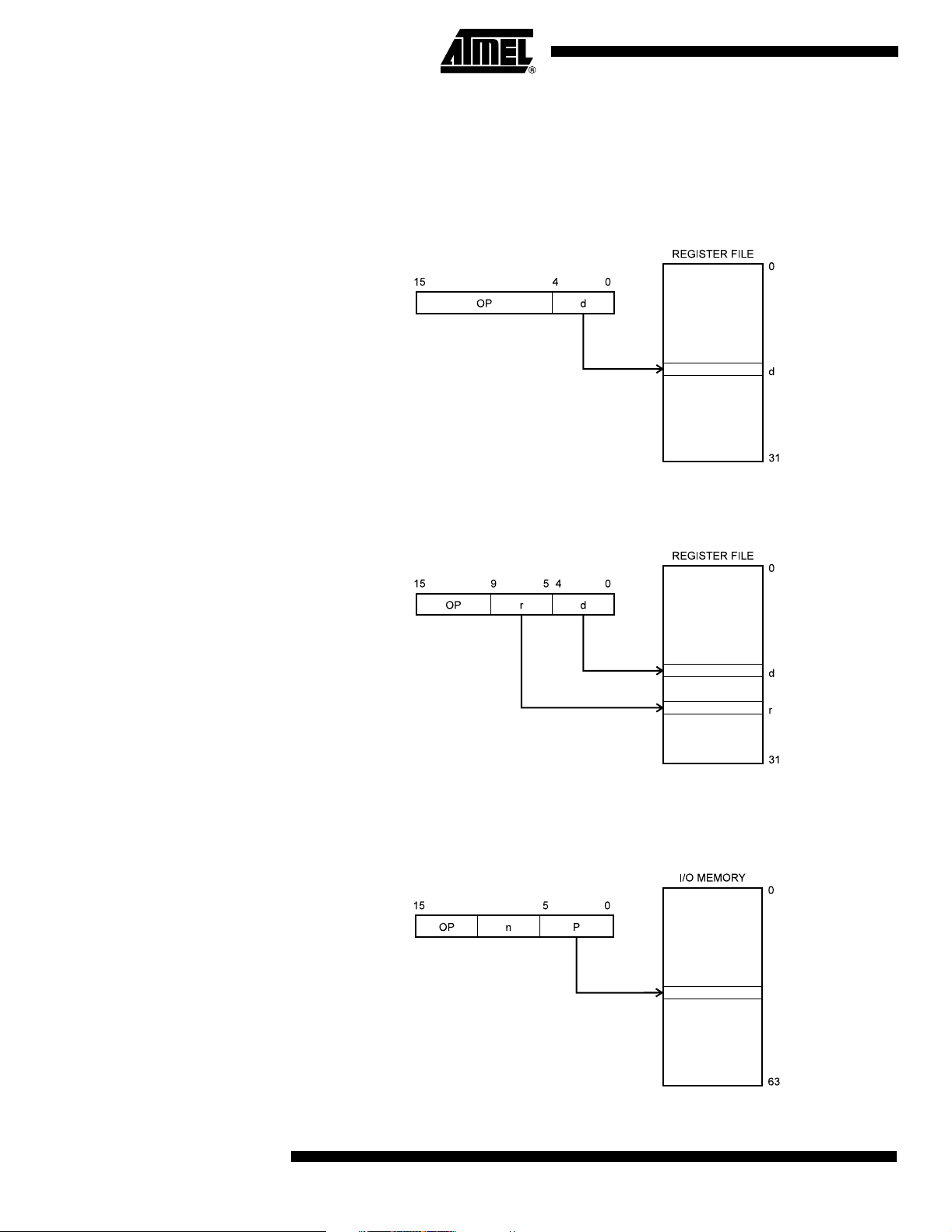
Register Direct, Single Register Rd
Register Direct, Two Registers Rd and Rr
Figure 9. Direct Single Register Addressing
The operand is contained in register d (Rd).
Figure 10. Direct Register Addressing, Two Registers
Operands are contained in register r (Rr) and d (Rd). The result is stored in register d
(Rd).
I/O Direct Figure 11. I/O Direct Addressing
10
AT90S2313
0839I–AVR–06/02
Page 11
Operand address is contained in 6 bits of the instruction word. n is the destination or
source register address.
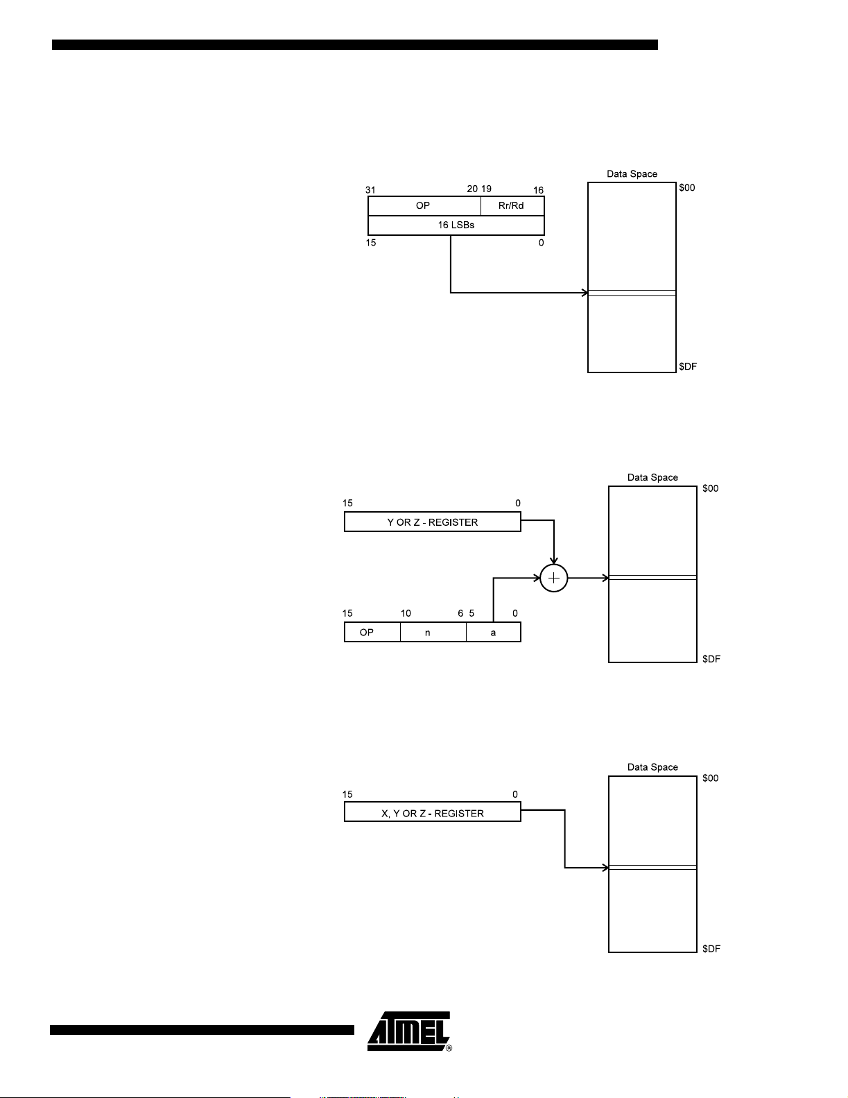
Data Direct Figure 12. Direct Data Addressing
A 16-bit data address is contained in the 16 LSBs of a 2-word instruction. Rd/Rr specify
the destination or source register.
AT90S2313
Data Indirect with Displacement
Data Indirect Figure 14. Data Indirect Addressing
Figure 13. Data Indirect with Displacement
Operand address is the result of the Y- or Z-register contents added to the address contained in 6 bits of the instruction word.
0839I–AVR–06/02
Operand address is the contents of the X-, Y-, or Z-register.
11
Page 12
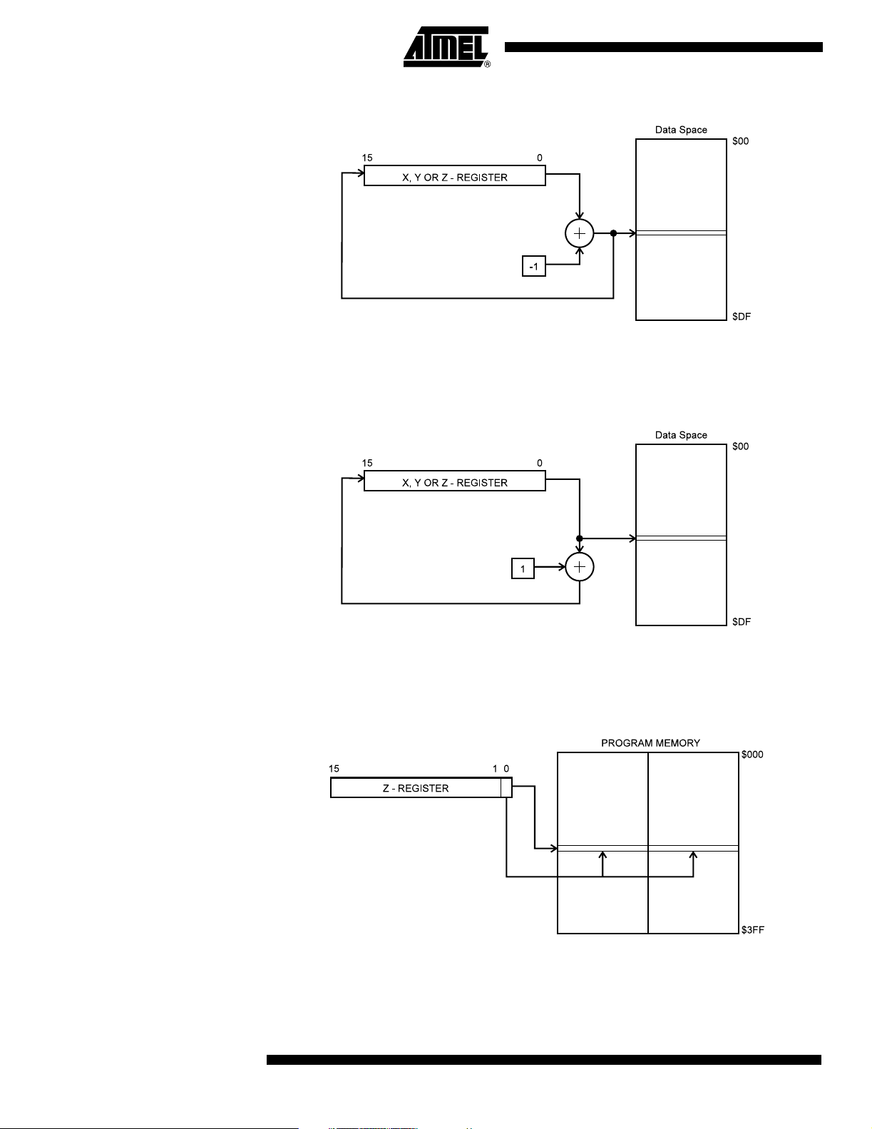
Data Indirect with Predecrement
Figure 15. Data Indirect Addressing with Pre-decrement
The X-, Y-, or Z-register is decremented before the operation. Operand address is the
decremented contents of the X-, Y-, or Z-register.
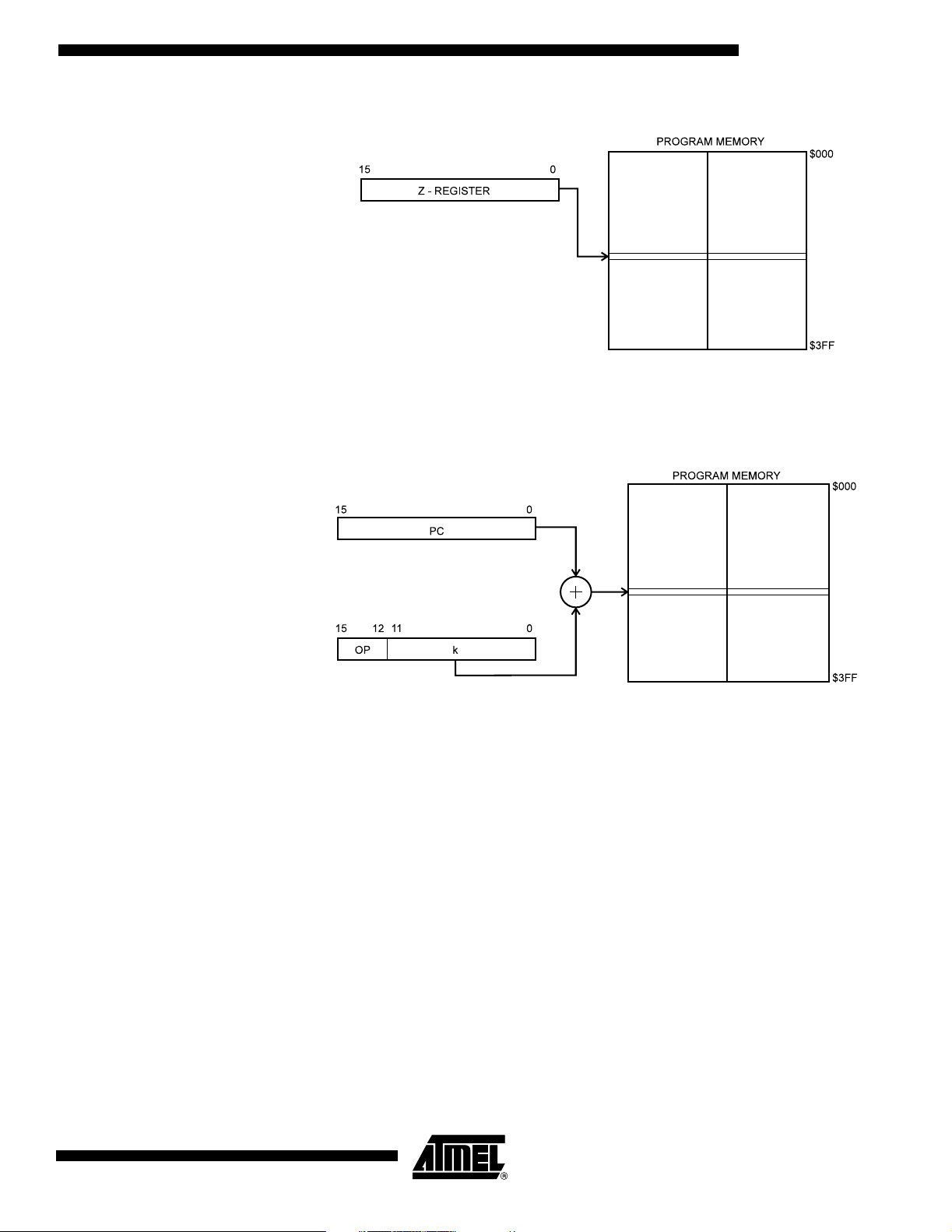
Data Indirect with Postincrement
Constant Addressing Using the LPM Instruction
Figure 16. Data Indirect Addressing with Post-increment
The X-, Y-, or Z-register is incremented after the operation. Operand address is the contents of the X-, Y-, or Z-register prior to incrementing.
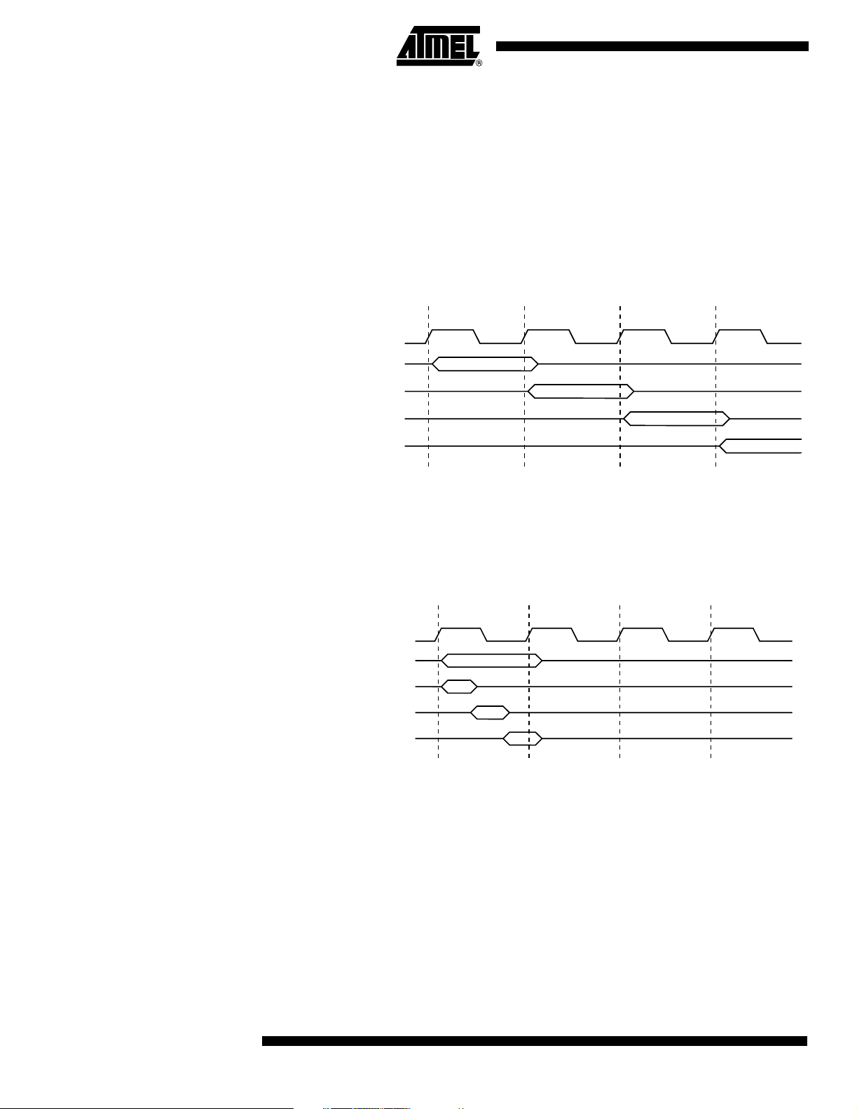
Figure 17. Code Memory Constant Addressing
12
Constant byte address is specified by the Z-register contents. The 15 MSBs select word
address (0 - 1K), the LSB selects low byte if cleared (LSB = 0) or high byte if set (LSB =
1).
AT90S2313
0839I–AVR–06/02
Page 13
AT90S2313
Indirect Program Addressing, IJMP and ICALL
Relative Program Addressing, RJMP and RCALL
Figure 18. Indirect Program Memory Addressing
Program execution continues at address contained by the Z-register (i.e., the PC is
loaded with the contents of the Z-register).
Figure 19. Relative Program Memory Addressing
0839I–AVR–06/02
Program execution continues at address PC + k + 1. The relative address k is -2048 to
2047.
13
Page 14
Memory Access and Instruction Execution Timing
This section describes the general access timing concepts for instruction execution and
internal memory access.
TheAVRCPUisdrivenbytheSystemClockØ, directly generated from the external
clock crystal for the chip. No internal clock division is used.
Figure 20 shows the parallel instruction fetches and instruction executions enabled by
the Harvard architecture and the fast-access Register File concept. This is the basic
pipelining concept to obtain up to 1 MIPS per MHz with the corresponding unique results
for functions per cost, functions per clocks and functions per power-unit.
Figure 20. The Parallel Instruction Fetches and Instruction Executions
T1 T2 T3 T4
System Clock Ø
1st Instruction Fetch
1st Instruction Execute
2nd Instruction Fetch
2nd Instruction Execute
3rd Instruction Fetch
3rd Instruction Execute
4th Instruction Fetch
Figure 21 shows the internal timing concept for the Register File. In a single clock cycle
an ALU operation using two register operands is executed, and the result is stored back
to the destination register.
Figure 21. Single-cycle ALU Operation
T1 T2 T3 T4
System Clock Ø
Total Execution Time
Register Operands Fetch
ALU Operation Execute
Result Write Back
The internal data SRAM access is performed in two System Clock cycles as described
in Figure 22.
14
AT90S2313
0839I–AVR–06/02
Page 15
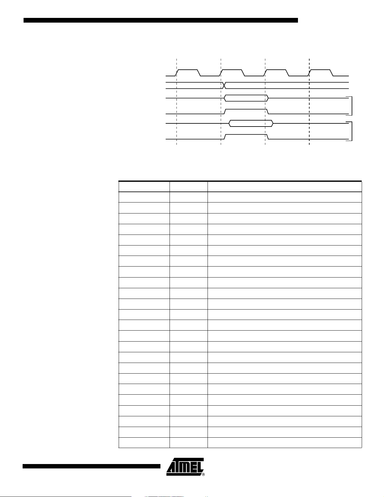
Figure 22. On-chip Data SRAM Access Cycles
T1 T2 T3 T4
System Clock Ø
AT90S2313
Address
Data
WR
Data
RD
Prev. Address
Address
I/O Memory The I/O space definition of the AT90S2313 is shown in Table 1.
Table 1. AT90S2313 I/O Space
Address Hex Name Function
$3F ($5F) SREG Status Register
$3D ($5D) SPL Stack Pointer Low
$3B ($5B) GIMSK General Interrupt MaSK Register
$3A ($5A) GIFR General Interrupt Flag Register
$39 ($59) TIMSK Timer/Counter Interrupt MaSK Register
$38 ($58) TIFR Timer/Counter Interrupt Flag Register
$35 ($55) MCUCR MCU general Control Register
(1)
Write
Read
$33 ($53) TCCR0 Timer/Counter 0 Control Register
$32 ($52) TCNT0 Timer/Counter 0 (8-bit)
$2F ($4F) TCCR1A Timer/Counter 1 Control Register A
$2E ($4E) TCCR1B Timer/Counter 1 Control Register B
$2D ($4D) TCNT1H Timer/Counter 1 High Byte
$2C ($4C) TCNT1L Timer/Counter 1 Low Byte
$2B ($4B) OCR1AH Output Compare Register 1 High Byte
$2A ($4A) OCR1AL Output Compare Register 1 Low Byte
$25 ($45) ICR1H T/C 1 Input Capture Register High Byte
$24 ($44) ICR1L T/C 1 Input Capture Register Low Byte
$21 ($41) WDTCR Watchdog Timer Control Register
$1E ($3E) EEAR EEPROM Address Register
$1D ($3D) EEDR EEPROM Data Register
$1C ($3C) EECR EEPROM Control Register
$18 ($38) PORTB Data Register, Port B
$17 ($37) DDRB Data Direction Register, Port B
$16 ($36) PINB Input Pins, Port B
0839I–AVR–06/02
15
Page 16
Table 1. AT90S2313 I/O Space
Address Hex Name Function
$12 ($32) PORTD Data Register, Port D
$11 ($31) DDRD Data Direction Register, Port D
$10 ($30) PIND Input Pins, Port D
$0C ($2C) UDR UART I/O Data Register
$0B ($2B) USR UART Status Register
$0A ($2A) UCR UART Control Register
$09 ($29) UBRR UART Baud Rate Register
$08 ($28) ACSR Analog Comparator Control and Status Register
Note: 1. Reserved and unused locations are not shown in the table.
(1)
(Continued)
All AT90S2313 I/O and peripherals are placed in the I/O space. The I/O locations are
accessed by the IN and OUT instructions transferring data between the 32 general purpose working registers and the I/O space. I/O Registers within the address range $00 $1F are directly bit-accessible using the SBI and CBI instructions. In these registers, the
value of single bits can be checked by using the SBIS and SBIC instructions. Refer to
the instruction set section for more details. When using the I/O specific commands IN
and OUT, the I/O addresses $00 - $3F must be used. When addressing I/O Registers as
SRAM, $20 must be added to this address. All I/O Register addresses throughout this
document are shown with the SRAM address in parentheses.
For compatibility with future devices, reserved bits should be written to zero if accessed.
Reserved I/O memory addresses should never be written.
Some of the Status Flags are cleared by writing a logical “1” to them. Note that the CBI
and SBI instructions will operate on all bits in the I/O Register, writing a “1” back into any
flag read as set, thus clearing the flag. The CBI and SBI instructions work with registers
$00 to $1F only.
The I/O and peripherals control registers are explained in the following sections.
Status Register – SREG The AVR Status Register (SREG) at I/O space location $3F ($5F) is defined as:
Bit 76543210
$3F ($5F) I THSVNZCSREG
Read/Write R/W R/W R/W R/W R/W R/W R/W R/W
Initialvalue00000000
• Bit 7 – I: Global Interrupt Enable
The Global Interrupt Enable bit must be set (one) for the interrupts to be enabled. The
individual interrupt enable control is then performed in separate control registers. If the
Global Interrupt Enable bit is cleared (zero), none of the interrupts are enabled independent of the individual interrupt enable settings. The I-bit is cleared by hardware after an
interrupt has occurred, and is set by the RETI instruction to enable subsequent
interrupts.
•Bit6–T:BitCopyStorage
16
The Bit Copy instructions BLD (Bit LoaD) and BST (Bit STore) use the T-bit as source
and destination for the operated bit. A bit from a register in the Register File can be copied into T by the BST instruction, and a bit in T can be copied into a bit in a register in the
Register File by the BLD instruction.
AT90S2313
0839I–AVR–06/02
Page 17

AT90S2313
• Bit 5 – H: Half-carry Flag
The Half-carry Flag H indicates a Half-carry in some arithmetic operations. See the
Instruction Set description for detailed information.
• Bit 4 – S: Sign Bit, S = N ⊕ V
The S-bit is always an exclusive or between the Negative Flag N and the Two’s Complement Overflow Flag V. See the Instruction Set description for detailed information.
• Bit 3 – V: Two’s Complement Overflow Flag
The Two’s Complement Overflow Flag V supports two’s complement arithmetics. See
the Instruction Set description for detailed information.
• Bit 2 – N: Negative Flag
The Negative Flag N indicates a negative result after the different arithmetic and logic
operations. See the Instruction Set description for detailed information.
• Bit 1 – Z: Zero Flag
The Zero Flag Z indicates a zero result after the different arithmetic and logic operations. See the Instruction Set description for detailed information.
• Bit 0 – C: Carry Flag
The Carry Flag C indicates a Carry in an arithmetic or logic operation. See the Instruction Set description for detailed information.
Note that the Status Register is not automatically stored when entering an interrupt routine and restored when returning from an interrupt routine. This must be handled by
software.
Stack Pointer – SP An 8-bit register at I/O address $3D ($5D) forms the Stack Pointer of the AT90S2313. 8
bits are used to address the 128 bytes of SRAM in locations $60 - $DF.
Bit 76543210
$3D ($5D) SP7 SP6 SP5 SP4 SP3 SP2 SP1 SP0 SPL
Read/Write R/W R/W R/W R/W R/W R/W R/W R/W
Initialvalue00000000
The Stack Pointer points to the data SRAM stack area where the Subroutine and Interrupt Stacks are located. This stack space in the data SRAM must be defined by the
program before any subroutine calls are executed or interrupts are enabled. The Stack
Pointer must be set to point above $60. The Stack Pointer is decremented by 1 when
data is pushed onto the stack with the PUSH instruction, and it is decremented by 2
when an address is pushed onto the stack with subroutine calls and interrupts. The
Stack Pointer is incremented by 1 when data is popped from the stack with the POP
instruction, and it is incremented by 2 when an address is popped from the stack with
return from subroutine RET or return from interrupt RETI.
0839I–AVR–06/02
17
Page 18

Reset and Interrupt Handling
The AT90S2313 provides 10 different interrupt sources. These interrupts and the separate Reset Vector each have a separate Program Vector in the program memory space.
All the interrupts are assigned individual enable bits that must be set (one) together with
the I-bit in the Status Register in order to enable the interrupt.
The lowest addresses in the Program memory space are automatically defined as the
Reset and Interrupt Vectors. The complete list of vectors is shown in Table 2. The list
also determines the priority levels of the different interrupts. The lower the address, the
higher the priority level. RESET has the highest priority, and next is INT0 (the External
Interrupt Request 0), etc.
Table 2. Reset and Interrupt Vectors
Vector No. Program Address Source Interrupt Definition
1 $000 RESET Hardware Pin, Power-on Reset and
Watchdog Reset
2 $001 INT0 External Interrupt Request 0
3 $002 INT1 External Interrupt Request 1
4 $003 TIMER1 CAPT1 Timer/Counter1 Capture Event
5 $004 TIMER1 COMP1 Timer/Counter1 Compare Match
6 $005 TIMER1 OVF1 Timer/Counter1 Overflow
7 $006 TIMER0 OVF0 Timer/Counter0 Overflow
8 $007 UART, RX UART, RX Complete
9 $008 UART, UDRE UART Data Register Empty
10 $009 UART, TX UART, TX Complete
11 $00A ANA_COMP Analog Comparator
The most typical and general program setup for the Reset and Interrupt Vector
addresses are:
Address Labels Code Comments
$000 rjmp RESET ; Reset Handler
$001 rjmp EXT_INT0 ; IRQ0 Handler
$002 rjmp EXT_INT1 ; IRQ1 Handler
$003 rjmp TIM_CAPT1 ; Timer1 Capture Handler
$004 rjmp TIM_COMP1 ; Timer1 Compare Handler
$005 rjmp TIM_OVF1 ; Timer1 Overflow Handler
$006 rjmp TIM_OVF0 ; Timer0 Overflow Handler
$007 rjmp UART_RXC ; UART RX Complete Handler
$008 rjmp UART_DRE ; UDR Empty Handler
$009 rjmp UART_TXC ; UART TX Complete Handler
$00a rjmp ANA_COMP ; Analog Comparator Handler
;
$00b MAIN: ldi r16,low(RAMEND); Main program start
$00c out SPL,r16
$00d <instr> xxx
…………
18
AT90S2313
0839I–AVR–06/02
Page 19
Reset Sources The AT90S2313 has three sources of reset:
• Power-on Reset. The MCU is reset when the supply voltage is below the Power-on
Reset threshold (V
POT
).
• External Reset. The MCU is reset when a low level is present on the RESET
more than 50 ns.
• Watchdog Reset. The MCU is reset when the Watchdog Timer period expires and
the Watchdog is enabled.
During Reset, all I/O Registers are then set to their initial values, and the program starts
execution from address $000. The instruction placed in address $000 must be an RJMP
(Relative Jump) instruction to the reset handling routine. If the program never enables
an interrupt source, the Interrupt Vectors are not used, and regular program code can
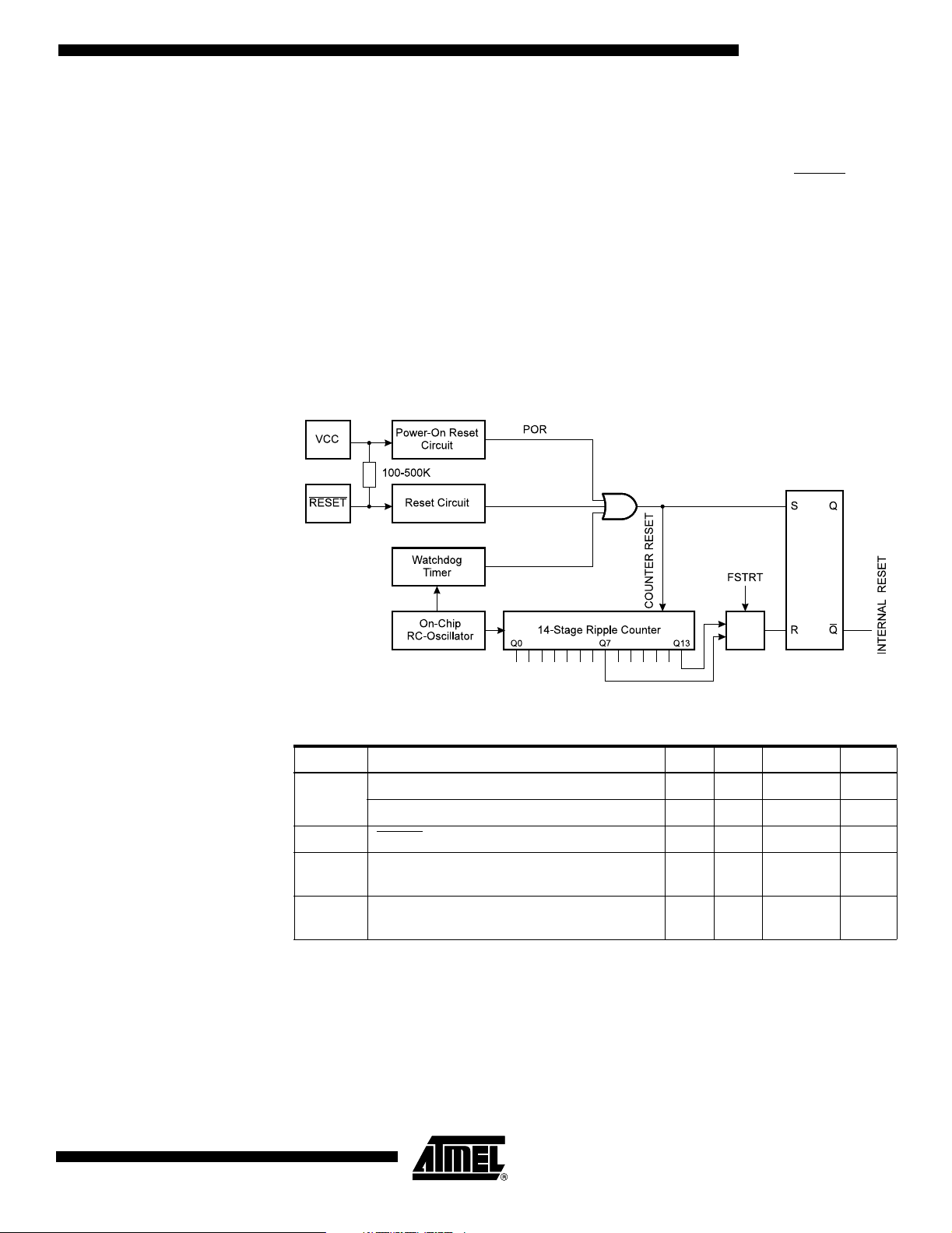
be placed at these locations. The circuit diagram in Figure 23 shows the reset logic.
Table 3 defines the timing and electrical parameters of the reset circuitry.
Figure 23. Reset Logic
AT90S2313
pin for
0839I–AVR–06/02
Table 3. Reset Characteristics (V
Symbol Parameter Min Typ Max Units
Power-on Reset Threshold Voltage (rising) 1.0 1.4 1.8 V
(1)
V
POT
V
RST
t
TOUT
t
TOUT
Note: 1. The Power-on Reset will not work unless the supply voltage has been below V
Power-on Reset Threshold Voltage (falling) 0.4 0.6 0.8 V
RESET Pin Threshold Voltage – 0.85 V
Reset Delay Time-out Period
FSTRT Unprogrammed
Reset Delay Time-out Period
FSTRT Programmed
(falling).
=5.0V)
CC
CC
11.0 16.0 21.0 ms
0.25 0.28 0.31 ms
V
POT
The user can select the start-up time according to typical Oscillator start-up. The number of WDT Oscillator cycles used for each time-out is shown in Table 4. The frequency
of the Watchdog Oscillator is voltage-dependent, as shown in “Typical Characteristics”
on page 74.
19
Page 20
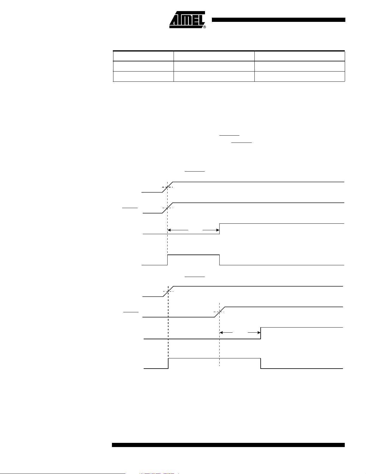
Table 4. Number of Watchdog Oscillator Cycles
FSTRT Time-out at VCC= 5V Number of WDT Cycles
Programmed 0.28 ms 256
Unprogrammed 16.0 ms 16K
Power-on Reset A Power-on Reset (POR) circuit ensures that the device is reset from Power-on. As
shown in Figure 23, an internal timer is clocked from the Watchdog Timer. This timer
prevents the MCU from starting until after a certain period after V
Power-on Threshold voltage (V
)(seeFigure24).TheFSTRTFusebitintheFlash
POT
has reached the
CC
can be programmed to give a shorter start-up time if a ceramic resonator or any other
fast-start Oscillator is used to clock the MCU.
If the built-in start-up delay is sufficient, RESET
an external pull-up resistor. By holding the RESET
can be connected to VCCdirectly or via
pin low for a period after VCChas
been applied, the Power-on Reset period can be extended. Refer to Figure 25 for a timing example of this.
Figure 24. MCU Start-up, RESET
V
VCC
RESET
TIME-OUT
INTERNAL
RESET
POT
V
RST
Figure 25. MCU Start-up, RESET
V
VCC
RESET
POT
Tied to VCC.
t
TOUT
Controlled Externally
V
RST
20
AT90S2313
TIME-OUT
INTERNAL
RESET
t
TOUT
0839I–AVR–06/02
Page 21
AT90S2313
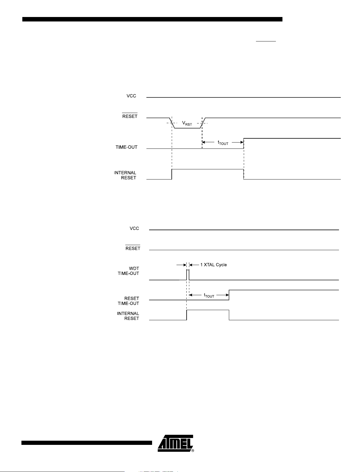
External Reset An External Reset is generated by a low level on the RESET pin. Reset pulses longer
than 50 ns will generate a reset, even if the clock is not running. Shorter pulses are not
guaranteed to generate a reset. When the applied signal reaches the Reset Threshold
Voltage (V
period t
Figure 26. External Reset during Operation
) on its positive edge, the delay timer starts the MCU after the Time-out
RST
has expired.
TOUT
Watchdog Reset When the Watchdog times out, it will generate a short reset pulse of one XTAL cycle
duration. On the falling edge of this pulse, the delay timer starts counting the Time-out
period t
. Refer to page 37 for details on operation of the Watchdog.
TOUT
Figure 27. Watchdog Reset during Operation
Interrupt Handling The AT90S2313 has two 8-bit Interrupt Mask Control Registers: the GIMSK (General
Interrupt Mask Register) and the TIMSK (Timer/Counter Interrupt Mask Register).
When an interrupt occurs, the Global Interrupt Enable I-bit is cleared (zero) and all interrupts are disabled. The user software can set (one) the I-bit to enable interrupts. The Ibit is set (one) when a Return from Interrupt instruction (RETI) is executed.
0839I–AVR–06/02
For interrupts triggered by events that can remain static (e.g., the Output Compare
Register1 matching the value of Timer/Counter1), the Interrupt Flag is set when the
event occurs. If the Interrupt Flag is cleared and the interrupt condition persists, the flag
will not be set until the event occurs the next time.
When the Program Counter is vectored to the actual Interrupt Vector in order to execute
the interrupt handling routine, hardware clears the corresponding flag that generated the
21
Page 22
General Interrupt Mask Register – GIMSK
interrupt. Some of the Interrupt Flags can also be cleared by writing a logical “1” to the
flag bit position(s) to be cleared.
If an interrupt condition occurs when the corresponding interrupt enable bit is cleared
(zero), the Interrupt Flag will be set and remembered until the interrupt is enabled, or the
flag is cleared by software.
If one or more interrupt conditions occur when the Global Interrupt Enable bit is cleared
(zero), the corresponding interrupt flag(s) will be set and remembered until the Global
Interrupt Enable bit is set (one), and will be executed by order of priority.
Note that external level interrupt does not have a flag, and will only be remembered for
as long as the interrupt condition is active.
Note that the Status Register is not automatically stored when entering an interrupt routine and restored when returning from an interrupt routine. This must be handled by
software.
Bit 7 6 5 4 3 2 1 0
$3B ($5B) INT1 INT0 – – – – – – GIMSK
Read/Write R/W R/W R R R R R R
Initial value 0 0 0 0 0 0 0 0
• Bit 7 – INT1: External Interrupt Request 1 Enable
When the INT1 bit is set (one) and the I-bit in the Status Register (SREG) is set (one),
the external pin interrupt is enabled. The Interrupt Sense Control1 bits 1/0 (ISC11 and
ISC10) in the MCU general Control Register (MCUCR) defines whether the external
interrupt is activated on rising or falling edge of the INT1 pin or level sensed. Activity on
the pin will cause an interrupt request even if INT1 is configured as an output. The corresponding interrupt of External Interrupt Request 1 is executed from program memory
address $002. See also “External Interrupts”.
• Bit 6 – INT0: External Interrupt Request 0 Enable
When the INT0 bit is set (one) and the I-bit in the Status Register (SREG) is set (one),
the external pin interrupt is enabled. The Interrupt Sense Control0 bits 1/0 (ISC01 and
ISC00) in the MCU general Control Register (MCUCR) defines whether the External
Interrupt is activated on rising or falling edge of the INT0 pin or level sensed. Activity on
the pin will cause an interrupt request even if INT0 is configured as an output. The corresponding interrupt of External Interrupt Request 0 is executed from program memory
address $001. See also “External Interrupts.”
• Bits 5..0 – Res: Reserved Bits
These bits are reserved bits in the AT90S2313 and always read as zero.
22
AT90S2313
0839I–AVR–06/02
Page 23
General Interrupt FLAG Register – GIFR
AT90S2313
Bit 7 6 5 4 3 2 1 0
$3A ($5A) INTF1 INTF0 – – – – – – GIFR
Read/Write R/W R/W R R R R R R
Initial value 0 0 0 0 0 0 0 0
• Bit 7 – INTF1: External Interrupt Flag1
When an edge on the INT1 pin triggers an interrupt request, the corresponding Interrupt
Flag, INTF1, becomes set (one). If the I-bit in SREG and the corresponding interrupt
enable bit, INT1 bit in GIMSK, are set (one), the MCU will jump to the Interrupt Vector.
The flag is cleared when the interrupt routine is executed. Alternatively, the flag can be
cleared by writing a logical “1” to it. The flag is always cleared when INT1 is configured
as level interrupt.
• Bit 6 – INTF0: External Interrupt Flag0
When an edge on the INT0 pin triggers an interrupt request, the corresponding Interrupt
Flag, INTF0, becomes set (one). If the I-bit in SREG and the corresponding interrupt
enable bit, INT0 bit in GIMSK, are set (one), the MCU will jump to the Interrupt Vector.
The flag is cleared when the interrupt routine is executed. Alternatively, the flag can be
cleared by writing a logical “1” to it. The flag is always cleared when INT0 is configured
as level interrupt.
Timer/Counter Interrupt Mask Register – TIMSK
• Bits 5..0 – Res: Reserved Bits
These bits are reserved bits in the AT90S2313 and always read as zero.
Note that external level interrupt does not have a flag, and will only be remembered for
as long as the interrupt condition is active.
Bit 7 6 5 4 3 2 1 0
$39 ($59) TOIE1 OCIE1A – – TICIE1 – TOIE0 – TIMSK
Read/Write R/W R/W R R R/W R R/W R
Initial value 0 0 0 0 0 0 0 0
• Bit 7 – TOIE1: Timer/Counter1 Overflow Interrupt Enable
When the TOIE1 bit is set (one) and the I-bit in the Status Register is set (one), the
Timer/Counter1 Overflow Interrupt is enabled. The corresponding interrupt (at vector
$005) is executed if an overflow in Timer/Counter1 occurs (i.e., when the TOV1 bit is set
in the Timer/Counter Interrupt Flag Register [TIFR]).
• Bit 6 – OCIE1A: Timer/Counter1 Output Compare Match Interrupt Enable
When the OCIE1A bit is set (one) and the I-bit in the Status Register is set (one), the
Timer/Counter1 Compare Match Interrupt is enabled. The corresponding interrupt (at
vector $004) is executed if a compare match in Timer/Counter1 occurs (i.e., when the
OCF1A bit is set in the Timer/Counter Interrupt Flag Register [TIFR]).
0839I–AVR–06/02
• Bit 5,4 – Res: Reserved Bits
These bits are reserved bits in the AT90S2313 and always read as zero.
23
Page 24

Timer/Counter Interrupt FLAG Register – TIFR
• Bit 3 – TICIE1: Timer/Counter1 Input Capture Interrupt Enable
When the TICIE1 bit is set (one) and the I-bit in the Status Register is set (one), the
Timer/Counter1 Input Capture Event Interrupt is enabled. The corresponding interrupt
(at vector $003) is executed if a capture-triggering event occurs on PD6(ICP) (i.e., when
the ICF1 bit is set in the Timer/Counter Interrupt Flag Register [TIFR]).
• Bit 2 – Res: Reserved Bit
This bit is a reserved bit in the AT90S2313 and always reads as zero.
• Bit 1 – TOIE0: Timer/Counter0 Overflow Interrupt Enable
When the TOIE0 bit is set (one) and the I-bit in the Status Register is set (one), the
Timer/Counter0 Overflow Interrupt is enabled. The corresponding interrupt (at vector
$006) is executed if an overflow in Timer/Counter0 occurs (i.e., when the TOV0 bit is set
in the Timer/Counter Interrupt Flag Register [TIFR]).
• Bit 0 – Res: Reserved Bit
This bit is a reserved bit in the AT90S2313 and always read as zero.
Bit 7 6 5 4 3 2 1 0
$38 ($58) TOV1 OCF1A – – ICF1 – TOV0 – TIFR
Read/Write R/W R/W R R R/W R R/W R
Initial value 0 0 0 0 0 0 0 0
• Bit 7 – TOV1: Timer/Counter1 Overflow Flag
The TOV1 is set (one) when an overflow occurs in Timer/Counter1. TOV1 is cleared by
hardware when executing the corresponding interrupt handling vector. Alternatively,
TOV1 is cleared by writing a logical “1” to the flag. When the I-bit in SREG and TOIE1
(Timer/Counter1 Overflow Interrupt Enable) and TOV1 are set (one), the
Timer/Counter1 Overflow Interrupt is executed. In PWM mode, this bit is set when
Timer/Counter1 changes counting direction at $0000.
• Bit 6 – OCF1A: Output Compare Flag 1A
The OCF1A bit is set (one) when a compare match occurs between the Timer/Counter1
and the data in OCR1A (Output Compare Register1 A). OCF1A is cleared by hardware
when executing the corresponding interrupt handling vector. Alternatively, OCF1A is
cleared by writing a logical “1” to the flag. When the I-bit in SREG and OCIE1A
(Timer/Counter1 Compare Match Interrupt Enable) and the OCF1A are set (one), the
Timer/Counter1 Compare Match Interrupt is executed.
• Bits 5, 4 – Res: Reserved Bits
These bits are reserved bits in the AT90S2313 and always read as zero.
• Bit 3 – ICF1: Input Capture Flag 1
The ICF1 bit is set (one) to flag an input capture event, indicating that the
Timer/Counter1 value has been transferred to the Input Capture Register (ICR1). ICF1
is cleared by hardware when executing the corresponding interrupt handling vector.
Alternatively, ICF1 is cleared by writing a logical “1” to the flag. When the SREG I-bit
and TICIE1 (Timer/Counter1 Input Capture Interrupt Enable) and ICF1 are set (one), the
Timer/Counter1 Capture Interrupt is executed.
24
AT90S2313
0839I–AVR–06/02
Page 25

AT90S2313
• Bit 2 – Res: Reserved Bit
This bit is a reserved bit in the AT90S2313 and always reads as zero.
• Bit 1 – TOV0: Timer/Counter0 Overflow Flag
The bit TOV0 is set (one) when an overflow occurs in Timer/Counter0. TOV0 is cleared
by hardware when executing the corresponding interrupt handling vector. Alternatively,
TOV0 is cleared by writing a logical “1” to the flag. When the SREG I-bit and TOIE0
(Timer/Counter0 Overflow Interrupt Enable) and TOV0 are set (one), the
Timer/Counter0 Overflow Interrupt is executed.
• Bit 0 – Res: Reserved Bit
This bit is a reserved bit in the AT90S2313 and always reads as zero.
External Interrupts The External Interrupts are triggered by the INT1 and INT0 pins. Observe that, if
enabled, the interrupts will trigger even if the INT0/INT1 pins are configured as outputs.
This feature provides a way of generating a software interrupt. The External Interrupts
can be triggered by a falling or rising edge or a low level. This is set up as indicated in
the specification for the MCU Control Register (MCUCR). When the External Interrupt is
enabled and is configured as level-triggered, the interrupt will trigger as long as the pin
is held low.
The External Interrupts are set up as described in the specification for the MCU Control
Register (MCUCR).
Interrupt Response Time The interrupt execution response for all the enabled AVR interrupts is four clock cycles,
minimum. Four clock cycles after the Interrupt Flag has been set, the Program Vector
address for the actual interrupt handling routine is executed. During this four clock cycle
period, the Program Counter (two bytes) is pushed onto the Stack, and the Stack
Pointer is decremented by two. The Power-down is normally a relative jump to the interrupt routine, and this jump takes two clock cycles. If an interrupt occurs during execution
of a multi-cycle instruction, this instruction is completed before the interrupt is served.
A return from an interrupt handling routine takes four clock cycles. During these four
clock cycles, the Program Counter (two bytes) is popped back from the Stack, the Stack
Pointer is incremented by two, and the I-flag in SREG is set. When the AVR exits from
an interrupt, it will always return to the main program and execute one more instruction
before any pending interrupt is served.
MCU Control Register – MCUCR
The MCU Control Register contains control bits for general MCU functions.
Bit 76543210
$35 ($55) – – SE SM ISC11 ISC10 ISC01 ISC00 MCUCR
Read/Write R R R/W R/W R/W R/W R/W R/W
Initialvalue00000000
• Bits 7, 6 – Res: Reserved Bits
0839I–AVR–06/02
These bits are reserved bits in the AT90S2313 and always read as zero.
• Bit 5 – SE: Sleep Enable
The SE bit must be set (one) to make the MCU enter the sleep mode when the SLEEP
instruction is executed. To avoid the MCU entering the sleep mode unless it is the programmer’s purpose, it is recommended to set the Sleep Enable (SE) bit just before the
execution of the SLEEP instruction.
25
Page 26
• Bit 4 – SM: Sleep Mode
This bit selects between the two available sleep modes. When SM is cleared (zero), Idle
mode is selected as sleep mode. When SM is set (one), Power-down mode is selected
as sleep mode. For details, refer to the paragraph “Sleep Modes”.
•Bits3,2–ISC11,ISC10:InterruptSenseControl1Bit1andBit0
The External Interrupt 1 is activated by the external pin INT1 if the SREG I-flag and the
corresponding interrupt mask in the GIMSK Register is set. The level and edges on the
external INT1 pin that activate the interrupt are defined in Table 5.
Table 5. Interrupt 1 Sense Control
ISC11 ISC10 Description
0 0 The low level of INT1 generates an interrupt request.
01Reserved
1 0 The falling edge of INT1 generates an interrupt request.
1 1 The rising edge of INT1 generates an interrupt request.
• Bits 1, 0 – ISC01, ISC00: Interrupt Sense Control 0 Bit 1 and Bit 0
The External Interrupt 0 is activated by the external pin INT0 if the SREG I-flag and the
corresponding interrupt mask is set. The level and edges on the external INT0 pin that
activate the interrupt are defined in Table 6.
Table 6. Interrupt 0 Sense Control
ISC01 ISC00 Description
0 0 The low level of INT0 generates an interrupt request.
01Reserved
1 0 The falling edge of INT0 generates an interrupt request.
1 1 The rising edge of INT0 generates an interrupt request.
The value on the INTn pin is sampled before detecting edges. If edge interrupt is
selected, pulses with a duration longer than one CPU clock period will generate an interrupt. Shorter pulses are not guaranteed to generate an interrupt. If low-level interrupt is
selected, the low level must be held until the completion of the currently executing
instruction to generate an interrupt. If enabled, a level-triggered interrupt will generate
an interrupt request as long as the pin is held low.
26
AT90S2313
0839I–AVR–06/02
Page 27
AT90S2313
Sleep Modes To enter the sleep modes, the SE bit in MCUCR must be set (one) and a SLEEP instruc-
tion must be executed. If an enabled interrupt occurs while the MCU is in a sleep mode,
the MCU awakes, executes the interrupt routine, and resumes execution from the
instruction following SLEEP. The contents of the Register File, SRAM and I/O memory
are unaltered. If a Reset occurs during sleep mode, the MCU wakes up and executes
from the Reset Vector.
Idle Mode When the SM bit is cleared (zero), the SLEEP instruction forces the MCU into the Idle
mode, stopping the CPU but allowing Timer/Counters, Watchdog and the interrupt system to continue operating. This enables the MCU to wake up from external triggered
interrupts as well as internal ones like Timer Overflow interrupt and Watchdog Reset. If
wake-up from the Analog Comparator Interrupt is not required, the Analog Comparator
can be powered down by setting the ACD-bit in the Analog Comparator Control and Status Register (ACSR). This will reduce power consumption in Idle mode. When the MCU
wakes up from Idle mode, the CPU starts program execution immediately.
Power-down Mode When the SM bit is set (one), the SLEEP instruction forces the MCU into the Power-
down mode. In this mode, the external Oscillator is stopped while the external interrupts
and the Watchdog (if enabled) continue operating. Only an External Reset, a Watchdog
Reset (if enabled), an external level interrupt on INT0 or INT1 can wake up the MCU.
Note that when a level-triggered interrupt is used for wake-up from Power-down, the low
level must be held for a time longer than the reset delay Time-out period t
wise, the device will not wake up.
TOUT
.Other-
Timer/Counters The AT90S2313 provides two general purpose Timer/Counters – one 8-bit T/C and one
16-bit T/C. The Timer/Counters have individual prescaling selection from the same 10bit prescaling timer. Both Timer/Counters can either be used as a timer with an internal
clock time base or as a counter with an external pin connection that triggers the
counting.
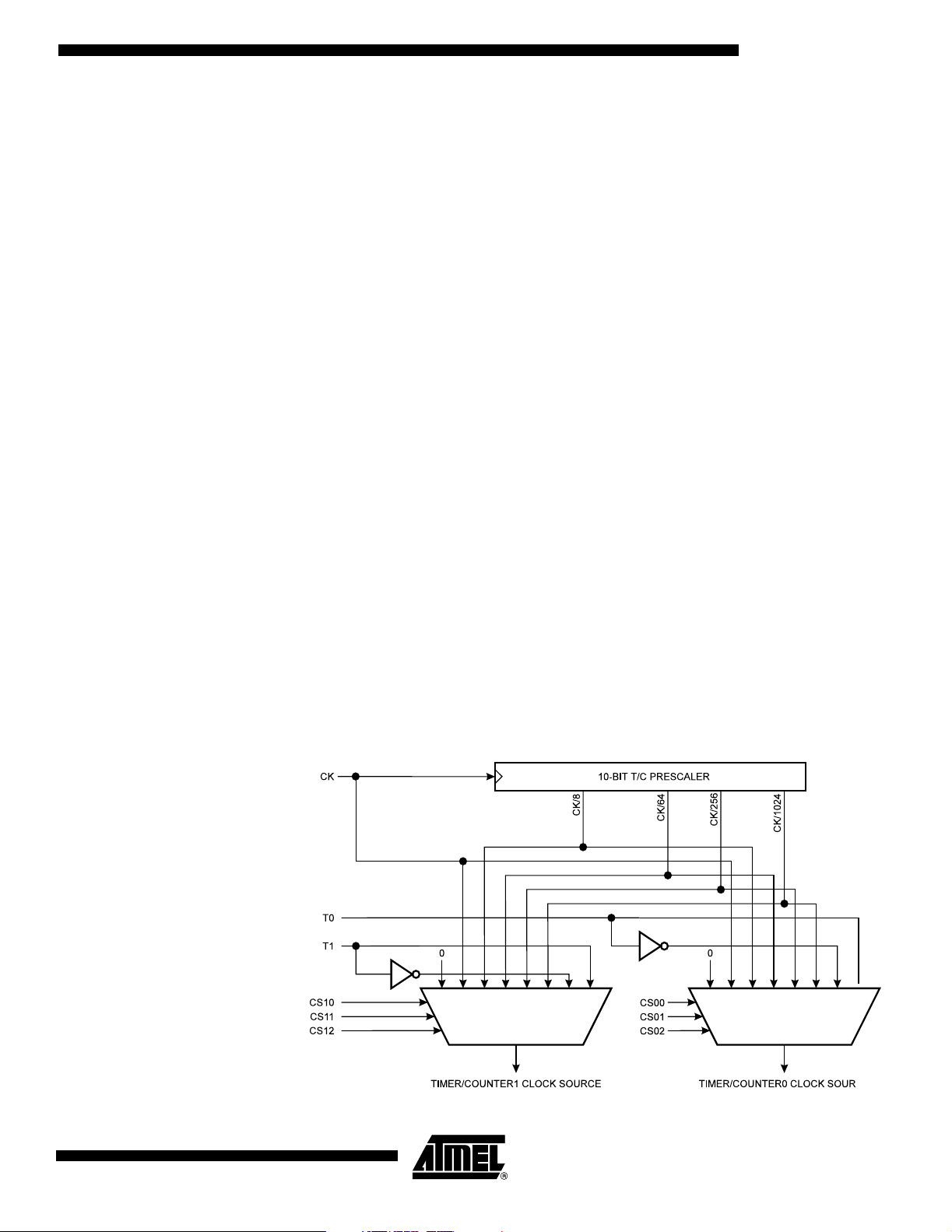
Timer/Counter Prescaler Figure 28 shows the general Timer/Counter prescaler.
Figure 28. Timer/Counter Prescaler
0839I–AVR–06/02
TCK1 TCK0
27
Page 28
The four different prescaled selections are: CK/8, CK/64, CK/256, and CK/1024, where
CK is the Oscillator clock. For the two Timer/Counters, added selections such as CK,
external clock source and stop can be selected as clock sources.
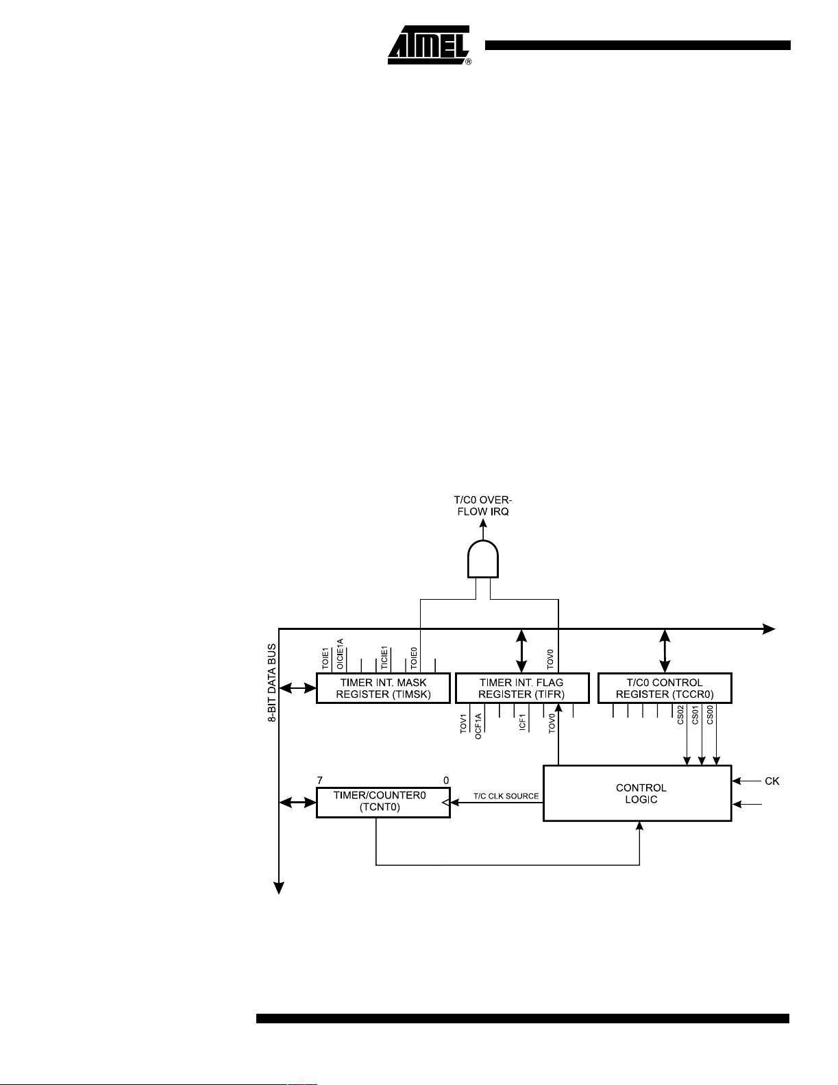
8-bit Timer/Counter0 Figure 29 shows the block diagram for Timer/Counter0.
The 8-bit Timer/Counter0 can select clock source from CK, prescaled CK or an external
pin. In addition, it can be stopped as described in the specification for the
Timer/Counter0 Control Register (TCCR0). The Overflow Status Flag is found in the
Timer/Counter Interrupt Flag Register (TIFR). Control signals are found in the
Timer/Counter0 Control Register (TCCR0). The interrupt enable/disable settings for
Timer/Counter0 are found in the Timer/Counter Interrupt Mask Register (TIMSK).
When Timer/Counter0 is externally clocked, the external signal is synchronized with the
Oscillator frequency of the CPU. To assure proper sampling of the external clock, the
minimum time between two external clock transitions must be at least one internal CPU
clock period. The external clock signal is sampled on the rising edge of the internal CPU
clock.
The 8-bit Timer/Counter0 features both a high-resolution and a high-accuracy usage
with the lower prescaling opportunities. Similarly, the high prescaling opportunities make
the Timer/Counter0 useful for lower speed functions or exact timing functions with infrequent actions.
Figure 29. Timer/Counter0 Block Diagram
28
T0
AT90S2313
0839I–AVR–06/02
Page 29

Timer/Counter0 Control Register – TCCR0
AT90S2313
Bit 7 6 5 4 3 2 1 0
$33 ($53) –– – – –CS02 CS01 CS00 TCCR0
Read/Write R R R R R R/W R/W R/W
Initial value 0 0 0 0 0 0 0 0
• Bits 7..3 – Res: Reserved Bits
These bits are reserved bits in the AT90S2313 and always read zero.
• Bits 2,1,0 – CS02, CS01, CS00: Clock Select0, Bit 2,1 and 0
The Clock Select0 bits 2, 1, and 0 define the prescaling source of Timer/Counter0.
Table 7. Clock 0 Prescale Select
CS02 CS01 CS00 Description
0 0 0 Stop, the Timer/Counter0 is stopped.
001CK
010CK/8
011CK/64
Timer/Counter0 – TCNT0
100CK/256
1 0 1 CK/1024
1 1 0 External Pin T0, falling edge
1 1 1 External Pin T0, rising edge
The Stop condition provides a Timer Enable/Disable function. The CK down divided
modes are scaled directly from the CK Oscillator clock. If the external pin modes are
used for Timer/Counter0, transitions on PD4/(T0) will clock the counter even if the pin is
configured as an output. This feature can give the user software control of the counting.
Bit 76543210
$32 ($52) MSB LSB TCNT0
Read/Write R/W R/W R/W R/W R/W R/W R/W R/W
Initialvalue00000000
The Timer/Counter0 is realized as an up-counter with read and write access. If the
Timer/Counter0 is written and a clock source is present, the Timer/Counter0 continues
counting in the timer clock cycle following the write operation.
0839I–AVR–06/02
29
Page 30

16-bit Timer/Counter1 Figure 30 shows the block diagram for Timer/Counter1.
Figure 30. Timer/Counter1 Block Diagram
T1
30
The 16-bit Timer/Counter1 can select clock source from CK, prescaled CK or an external pin. In addition, it can be stopped as described in the specification for the
Timer/Counter1 Control Register (TCCR1B). The different Status Flags (Overflow, Compare Match and Capture Event) and control signals are found in the Timer/Counter
Interrupt Flag Register (TIFR). The interrupt enable/disable settings for Timer/Counter1
are found in the Timer/Counter Interrupt Mask Register (TIMSK).
When Timer/Counter1 is externally clocked, the external signal is synchronized with the
Oscillator frequency of the CPU. To assure proper sampling of the external clock, the
minimum time between two external clock transitions must be at least one internal CPU
clock period. The external clock signal is sampled on the rising edge of the internal CPU
clock.
The 16-bit Timer/Counter1 features both a high-resolution and a high-accuracy usage
with the lower prescaling opportunities. Similarly, the high prescaling opportunities
makes the Timer/Counter1 useful for lower speed functions or exact timing functions
with infrequent actions.
The Timer/Counter1 supports an Output Compare function using the Output Compare
Register 1A (OCR1A) as the data source to be compared to the Timer/Counter1 contents. The Output Compare functions include optional clearing of the counter on
compare matches, and actions on the Output Compare pin 1 on compare matches.
AT90S2313
0839I–AVR–06/02
Page 31

AT90S2313
Timer/Counter1 can also be used as an 8-, 9-, or 10-bit Pulse Width Modulator. In this
mode the counter and the OCR1 Register serve as a glitch-free standalone PWM with
centered pulses. Refer to page 35 for a detailed description of this function.
The Input Capture function of Timer/Counter1 provides a capture of the Timer/Counter1
contents to the Input Capture Register (ICR1), triggered by an external event on the
Input Capture Pin (ICP). The actual capture event settings are defined by the
Timer/Counter1 Control Register (TCCR1B). In addition, the Analog Comparator can be
set to trigger the input capture. Refer to “Analog Comparator” on page 48 for details on
this. The ICP pin logic is shown in Figure 31.
Figure 31. ICP Pin Schematic Diagram
Timer/Counter1 Control Register A – TCCR1A
If the Noise Canceler function is enabled, the actual trigger condition for the capture
event is monitored over four samples, and all four must be equal to activate the capture
flag.
Bit 7 6 5 4 3 2 1 0
$2F ($4F) COM1A1 COM1A0 ––––PWM11 PWM10 TCCR1A
Read/Write R/W R/W R R R R R/W R/W
Initial value 0 0 0 0 0 0 0 0
• Bits 7, 6 – COM1A1, COM1A0: Compare Output Mode1, Bits 1 and 0
The COM1A1 and COM1A0 control bits determine any output pin action following a
compare match in Timer/Counter1. Any output pin actions affect pin OC1 (Output Compare pin 1) (PB3). This is an alternative function to the I/O port, and the corresponding
direction control bit must be set (one) to control an output pin. The control configuration
is shown in Table 8.
Table 8. Compare 1 Mode Select
COM1A1 COM1A0 Description
0 0 Timer/Counter1 disconnected from output pin OC1
0 1 Toggle the OC1 output line.
1 0 Clear the OC1 output line (to zero).
(1)(2)
0839I–AVR–06/02
1 1 Set the OC1 output line (to one).
Notes: 1. In PWM mode, these bits have a different function. Refer to Table 12 for a detailed
description.
2. The initial state of the OC1 output line is undefined.
• Bits 5..2 – Res: Reserved Bits
These bits are reserved bits in the AT90S2313 and always read zero.
31
Page 32

Timer/Counter1 Control Register B – TCCR1B
• Bits 1, 0 – PWM11, PWM10: Pulse Width Modulator Select Bits
These bits select PWM operation of Timer/Counter1 as specified in Table 9. This mode
is described on page 35.
Table 9. PWM Mode Select
PWM11 PWM10 Description
0 0 PWM operation of Timer/Counter1 is disabled
0 1 Timer/Counter1 is an 8-bit PWM
1 0 Timer/Counter1 is a 9-bit PWM
1 1 Timer/Counter1 is a 10-bit PWM
Bit 7654 3210
$2E ($4E) ICNC1 ICES1 ––CTC1 CS12 CS11 CS10 TCCR1B
Read/Write R/W R/W R R R/W R/W R/W R/W
Initialvalue0000 0000
• Bit 7 – ICNC1: Input Capture1 Noise Canceler (4 CKs)
When the ICNC1 bit is cleared (zero), the input capture trigger noise canceler function is
disabled. The input capture is triggered at the first rising/falling edge sampled on the ICP
(input capture pin) as specified. When the ICNC1 bit is set (one), four successive samples are measured on the ICP (input capture pin), and all samples must be high/low
according to the input capture trigger specification in the ICES1 bit. The actual sampling
frequency is the XTAL clock frequency.
• Bit 6 – ICES1: Input Capture1 Edge Select
While the ICES1 bit is cleared (zero), the Timer/Counter1 contents are transferred to the
Input Capture Register (ICR1) on the falling edge of the input capture pin (ICP). While
the ICES1 bit is set (one), the Timer/Counter1 contents are transferred to the Input Capture Register (ICR1) on the rising edge of the input capture pin (ICP).
• Bits 5, 4 – Res: Reserved Bits
These bits are reserved bits in the AT90S2313 and always read zero.
• Bit 3 – CTC1: Clear Timer/Counter1 on Compare Match
When the CTC1 control bit is set (one), the Timer/Counter1 is reset to $0000 in the clock
cycle after a compareA match. If the CTC1 control bit is cleared, Timer/Counter1 continues counting and is unaffected by a compare match. Since the compare match is
detected in the CPU clock cycle following the match, this function will behave differently
when a prescaling higher than 1 is used for the timer. When a prescaling of 1 is used,
and the Compare A Register is set to C, the timer will count as follows if CTC1 is set:
...|C-2|C-1|C|0|1|...
When the prescaler is set to divide by 8, the timer will count like this:
... | C-2, C-2, C-2, C-2, C-2, C-2, C-2, C-2 | C-1, C-1, C-1, C-1, C-1, C-1, C-1, C-1 | C, 0,
0, 0, 0, 0, 0, 0 |...
In PWM mode, this bit has no effect.
32
AT90S2313
0839I–AVR–06/02
Page 33

AT90S2313
• Bits 2,1,0 – CS12, CS11, CS10: Clock Select1, Bits 2, 1 and 0
The Clock Select1 bits 2, 1, and 0 define the prescaling source of Timer/Counter1.
Table 10. Clock 1 Prescale Select
CS12 CS11 CS10 Description
0 0 0 Stop, the Timer/Counter1 is stopped.
001CK
010CK/8
011CK/64
100CK/256
1 0 1 CK/1024
1 1 0 External Pin T1, falling edge
1 1 1 External Pin T1, rising edge
The Stop condition provides a Timer Enable/Disable function. The CK down divided
modes are scaled directly from the CK Oscillator clock. If the external pin modes are
used for Timer/Counter1, transitions on PD5/(T1) will clock the counter even if the pin is
configured as an output. This feature can give the user software control of the counting.
Timer/Counter1 – TCNT1H and TCNT1L
Bit 151413121110 9 8
$2D ($4D) MSB TCNT1H
$2C ($4C) LSB TCNT1L
76543210
Read/Write R/W R/W R/W R/W R/W R/W R/W R/W
R/W R/W R/W R/W R/W R/W R/W R/W
Initialvalue00000000
00000000
This 16-bit register contains the prescaled value of the 16-bit Timer/Counter1. To
ensure that both the high and low bytes are read and written simultaneously when the
CPU accesses these registers, the access is performed using an 8-bit temporary register (TEMP). This temporary register is also used when accessing OCR1A and ICR1. If
the main program and interrupt routines perform access to registers using TEMP, interrupts must be disabled during access from the main program or interrupts if interrupts
are re-enabled.
• TCNT1 Timer/Counter1 Write:
WhentheCPUwritestothehighbyteTCNT1H,thewrittendataisplacedinthe
TEMP Register. Next, when the CPU writes the low byte TCNT1L, this byte of data
is combined with the byte data in the TEMP Register, and all 16 bits are written to
the TCNT1 Timer/Counter1 Register simultaneously. Consequently, the high byte
TCNT1H must be accessed first for a full 16-bit register write operation.
• TCNT1 Timer/Counter1 Read:
When the CPU reads the low byte TCNT1L, the data of the low byte TCNT1L is sent
to the CPU and the data of the high byte TCNT1H is placed in the TEMP Register.
When the CPU reads the data in the high byte TCNT1H, the CPU receives the data
in the TEMP Register. Consequently, the low byte TCNT1L must be accessed first
for a full 16-bit register read operation.
0839I–AVR–06/02
33
Page 34

Timer/Counter1 Output Compare Register A – OCR1AH and OCR1AL
The Timer/Counter1 is realized as an up or up/down (in PWM mode) counter with read
and write access. If Timer/Counter1 is written to and a clock source is selected, the
Timer/Counter1 continues counting in the timer clock cycle after it is preset with the written value.
Bit 151413121110 9 8
$2B ($4B) MSB OCR1AH
$2A ($4A) LSB OCR1AL
76543210
Read/Write R/W R/W R/W R/W R/W R/W R/W R/W
R/W R/W R/W R/W R/W R/W R/W R/W
Initialvalue00000000
00000000
The Output Compare Register is a 16-bit read/write register.
The Timer/Counter1 Output Compare Register contains the data to be continuously
compared with Timer/Counter1. Actions on compare matches are specified in the
Timer/Counter1 Control and Status Registers.
Since the Output Compare Register (OCR1A) is a 16-bit register, a temporary register
TEMP is used when OCR1A is written to ensure that both bytes are updated simultaneously. When the CPU writes the high byte, OCR1AH, the data is temporarily stored in
the TEMP Register. When the CPU writes the low byte, OCR1AL, the TEMP Register is
simultaneously written to OCR1AH. Consequently, the high byte OCR1AH must be written first for a full 16-bit register write operation.
Timer/Counter1 Input Capture Register – ICR1H and ICR1L
The TEMP Register is also used when accessing TCNT1, and ICR1. If the main program and interrupt routines perform access to registers using TEMP, interrupts must be
disabled during access from the main program or interrupts if interrupts are re-enabled.
Bit 151413121110 9 8
$25 ($45) MSB ICR1H
$24 ($44) LSB ICR1L
76543210
Read/Write R R RRRRRR
RRRRRRRR
Initialvalue00000000
00000000
The Input Capture Register is a 16-bit read-only register.
When the rising or falling edge (according to the input capture edge setting [ICES1]) of
the signal at the input capture pin (ICP) is detected, the current value of the
Timer/Counter1 is transferred to the Input Capture Register (ICR1). At the same time,
the Input Capture Flag (ICF1) is set (one).
Since the Input Capture Register (ICR1) is a 16-bit register, a temporary register TEMP
is used when ICR1 is read to ensure that both bytes are read simultaneously. When the
CPU reads the low byte ICR1L, the data is sent to the CPU and the data of the high byte
ICR1H is placed in the TEMP Register. When the CPU reads the data in the high byte
ICR1H, the CPU receives the data in the TEMP Register. Consequently, the low byte
ICR1L must be accessed first for a full 16-bit register read operation.
34
AT90S2313
0839I–AVR–06/02
Page 35
AT90S2313
The TEMP Register is also used when accessing TCNT1 and OCR1A. If the main program and interrupt routines perform access to registers using TEMP, interrupts must be
disabled during access from the main program or interrupts if interrupts are re-enabled.
Timer/Counter1 in PWM Mode When the PWM mode is selected, Timer/Counter1 and the Output Compare Register1
(OCR1A) form an 8-, 9-, or 10-bit, free-running, glitch-free and phase-correct PWM with
output on the PB3(OC1) pin. Timer/Counter1 acts as an up/down counter, counting up
from $0000 to TOP (see Table 11), where it turns and counts down again to zero before
the cycle is repeated. When the counter value matches the contents of the 8, 9 or 10
least significant bits of OCR1A, the PB3(OC1) pin is set or cleared according to the settings of the COM1A1 and COM1A0 bits in the Timer/Counter1 Control Register
(TCCR1). Refer to Table 12 for details.
Table 11. Timer TOP Values and PWM Frequency
PWM Resolution Timer TOP Value Frequency
8-bit $00FF (255) f
9-bit $01FF (511) f
10-bit $03FF(1023) f
TC1
TC1
TC1
/510
/1022
/2046
Table 12. Compare1 Mode Select in PWM Mode
COM1A1 COM1A0 Effect on OC1
0 0 Not connected
0 1 Not connected
10
11
Note: 1. The initial state of the OC1 output line is undefined.
Cleared on compare match, upcounting. Set on compare match,
down-counting (non-inverted PWM).
Cleared on compare match, downcounting. Set on compare match,
up-counting (inverted PWM).
(1)
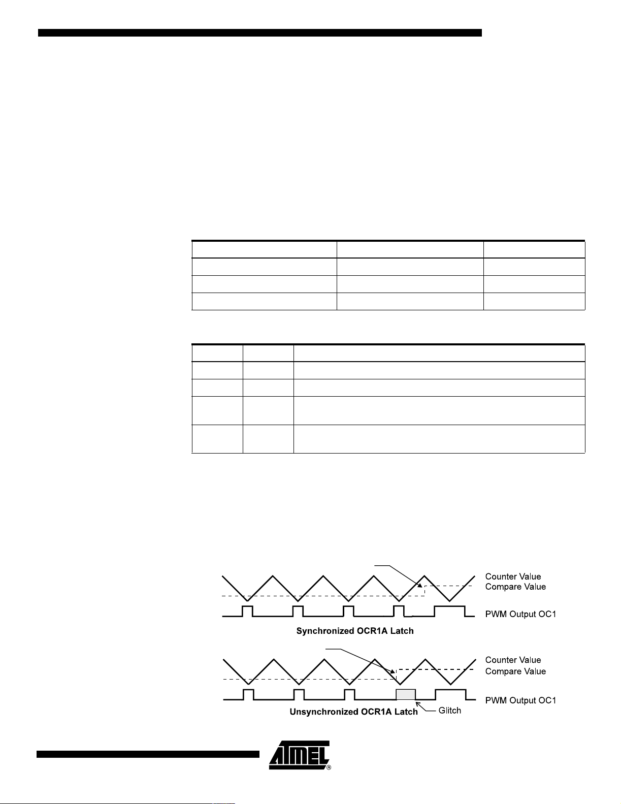
Note that in the PWM mode, the 10 least significant OCR1A bits, when written, are
transferred to a temporary location. They are latched when Timer/Counter1 reaches
TOP. This prevents the occurrence of odd-length PWM pulses (glitches) in the event of
an unsynchronized OCR1A write. See Figure 32 for an example.
Figure 32. Effects on Unsynchronized OCR1 Latching
Compare V
alue changes
0839I–AVR–06/02
Compare Value changes
35
Page 36
During the time between the write and the latch operations, a read from OCR1A will
read the contents of the temporary location. This means that the most recently written
value always will read out of OCR1A.
When the OCR1 contains $0000 or TOP, the output OC1 is updated to low or high on
the next compare match according to the settings of COM1A1/COM1A0. This is shown
in Table 13.
Note: If the Compare Register contains the TOP value and the prescaler is not in use
(CS12..CS10 = 001), the PWM output will not produce any pulse at all, because the upcounting and down-counting values are reached simultaneously. When the prescaler is in
use (CS12..CS10 ≠ 001 or 000), the PWM output goes active when the counter reaches
the TOP value, but the down-counting compare match is not interpreted to be reached
before the next time the counter reaches the TOP value, making a one-period PWM
pulse.
Table 13. PWM Outputs OCR = $0000 or TOP
COM1A1 COM1A0 OCR1A Output OC1
1 0 $0000 L
10TOPH
1 1 $0000 H
11TOPL
In PWM mode, the Timer Overflow Flag1 (TOV1) is set when the counter advances from
$0000. Timer Overflow Interrupt1 operates exactly as in normal Timer/Counter mode
(i.e., it is executed when TOV1 is set, provided that Timer Overflow Interrupt1 and global
interrupts are enabled). This also applies to the Timer Output Compare1 Flag and
interrupt.
36
AT90S2313
0839I–AVR–06/02
Page 37
AT90S2313
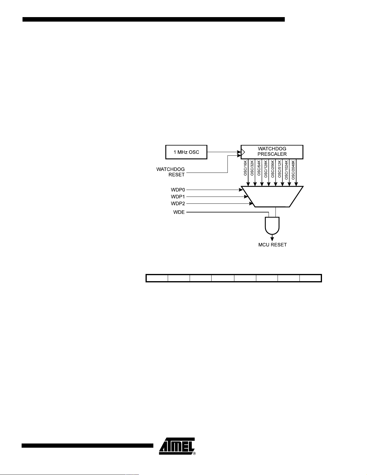
Watchdog Timer The Watchdog Timer is clocked from a separate On-chip Oscillator that runs at 1 MHz.
This is the typical value at V
V
levels. By controlling the Watchdog Timer prescaler, the Watchdog Reset interval
CC
can be adjusted. See Table 14 for a detailed description. The WDR (Watchdog Reset)
instruction resets the Watchdog Timer. Eight different clock cycle periods can be
selected to determine the reset period. If the reset period expires without another
Watchdog Reset, the AT90S2313 resets and executes from the Reset Vector. For timing details on the Watchdog Reset, refer to page 21.
To prevent unintentional disabling of the Watchdog, a special turn-off sequence must be
followed when the Watchdog is disabled. Refer to the description of the Watchdog Timer
Control Register for details.
Figure 33. Watchdog Timer
= 5V. See characterization data for typical values at other
CC
Watchdog Timer Control Register – WDTCR
Bit 765 4 3210
$21 ($41) –––WDTOE WDE WDP2 WDP1 WDP0 WDTCR
Read/Write R R R R/W R/W R/W R/W R /W
Initialvalue000 0 0000
• Bits 7..5 – Res: Reserved Bits
These bits are reserved bits in the AT90S2313 and will always read as zero.
• Bit 4 – WDTOE: Watchdog Turn-off Enable
This bit must be set (one) when the WDE bit is cleared. Otherwise, the Watchdog will
not be disabled. Once set, hardware will clear this bit to zero after four clock cycles.
Refer to the description of the WDE bit for a Watchdog disable procedure.
• Bit 3 – WDE: Watchdog Enable
When the WDE is set (one) the Watchdog Timer is enabled, and if the WDE is cleared
(zero), the Watchdog Timer function is disabled. WDE can only be cleared if the
WDTOE bit is set (one). To disable an enabled Watchdog Timer, the following procedure must be followed:
0839I–AVR–06/02
37
Page 38

1. In the same operation, write a logical “1” to WDTOE and WDE. A logical “1” must
be written to WDE even though it is set to 1 before the disable operation starts.
2. Within the next four clock cycles, write a logical “0” to WDE. This disables the
Watchdog.
• Bits 2..0 – WDP2, WDP1, WDP0: Watchdog Timer Prescaler 2, 1 and 0
The WDP2, WDP1 and WDP0 bits determine the Watchdog Timer prescaling when the
Watchdog Timer is enabled. The different prescaling values and their corresponding
time-out periods are shown in Table 14.
Table 14. Watchdog Timer Prescale Select
Number of
WDT Oscillator
WDP2 WDP1 WDP0
0 0 0 16K cycles 47 ms 15 ms
0 0 1 32K cycles 94 ms 30 ms
0 1 0 64K cycles 0.19 s 60 ms
0 1 1 128K cycles 0.38 s 0.12 s
1 0 0 256K cycles 0.75 s 0,24 s
1 0 1 512K cycles 1.5 s 0.49 s
1 1 0 1,024K cycles 3.0 s 0.97 s
1 1 1 2,048K cycles 6.0 s 1.9 s
Note: 1. The frequency of the Watchdog Oscillator is voltage-dependent, as shown in the
Electrical Characteristics section.
The WDR (Watchdog Reset) instruction should always be executed before the
Watchdog Timer is enabled. This ensures that the reset period will be in accordance
with the Watchdog Timer prescale settings. If the Watchdog Timer is enabled without
reset, the Watchdog Timer may not start counting from zero.
To avoid unintentional MCU Reset, the Watchdog Timer should be disabled or reset
before changing the Watchdog Timer Prescale Select.
Cycles
(1)
Typical Time-out
at V
CC
=3.0V
Typical Time-out
at VCC=5.0V
38
AT90S2313
0839I–AVR–06/02
Page 39

AT90S2313
EEPROM Read/Write Access
EEPROM Address Register – EEAR
The EEPROM Access Registers are accessible in the I/O space.
The write access time is in the range of 2.5 - 4 ms, depending on the V
voltages. A
CC
self-timing function, however, lets the user software detect when the next byte can be
written. If the user code contains code that writes the EEPROM, some precaution must
be taken. In heavily filtered power supplies, V
is likely to rise or fall slowly on Power-
CC
up/down. This causes the device for some period of time to run at a voltage lower than
specified as minimum for the clock frequency used. CPU operation under these conditions may cause the Program Counter to perform unintentional jumps and eventually
execute the EEPROM write code. To secure EEPROM integrity, the user is advised to
use an external under-voltage reset circuit in this case.
In order to prevent unintentional EEPROM writes, a specific write procedure must be followed. Refer to the description of the EEPROM Control Register for details on this.
When the EEPROM is written, the CPU is halted for two clock cycles before the next
instruction is executed. When the EEPROM is read, the CPU is halted for four clock
cycles before the next instruction is executed.
Bit 76543210
$1E ($3E) – EEAR6 EEAR5 EEAR4 EEAR3 EEAR2 EEAR1 EEAR0 EEAR
Read/Write R R/W R/W R/W R/W R/W R/W R/W
Initialvalue00000000
• Bit 7 – Res: Reserved Bit
EEPROM Data Register – EEDR
This bit is a reserved bit in the AT90S2313 and will always read as zero.
• Bit 6..0 – EEAR6..0: EEPROM Address
The EEPROM Address Register (EEAR6..0) specifies the EEPROM address in the 128
bytes EEPROM space. The EEPROM data bytes are addressed linearly between 0 and
127.
Bit 76543210
$1D ($3D) MSB LSB EEDR
Read/Write R/W R/W R/W R/W R/W R/W R/W R/W
Initialvalue00000000
• Bit 7..0 – EEDR7..0: EEPROM Data
For the EEPROM write operation, the EEDR Register contains the data to be written to
the EEPROM in the address given by the EEAR Register. For the EEPROM read operation, the EEDR contains the data read out from the EEPROM at the address given by
EEAR.
0839I–AVR–06/02
39
Page 40

EEPROM Control Register – EECR
Bit 76543 210
$1C ($3C) –––––EEMWE EEWE EERE EECR
Read/Write R RRRRR/WR/WR/W
Initialvalue00000 0 00
• Bit 7..3 – Res: Reserved Bits
These bits are reserved bits in the AT90S2313 and will always read as zero.
• Bit 2 – EEMWE: EEPROM Master Write Enable
The EEMWE bit determines whether setting EEWE to one causes the EEPROM to be
written. When EEMWE is set (one), setting EEWE will write data to the EEPROM at the
selected address. If EEMWE is zero, setting EEWE will have no effect. When EEMWE
has been set (one) by software, hardware clears the bit to zero after four clock cycles.
See the description of the EEWE bit for a EEPROM write procedure.
• Bit 1 – EEWE: EEPROM Write Enable
The EEPROM Write Enable Signal (EEWE) is the write strobe to the EEPROM. When
address and data are correctly set up, the EEWE bit must be set to write the value into
the EEPROM. The EEMWE bit must be set when the logical “1” iswrittentoEEWE,otherwise no EEPROM write takes place. The following procedure should be followed
when writing the EEPROM (the order of steps 2 and 3 is unessential):
1. Wait until EEWE becomes zero.
2. Write new EEPROM address to EEAR (optional).
3. Write new EEPROM data to EEDR (optional).
4. Write a logical “1” to the EEMWE bit in EECR (to be able to write a logical “1” to
theEEMWEbit,theEEWEbitmustbewrittentozerointhesamecycle).
5. Within four clock cycles after setting EEMWE, write a logical “1” to EEWE.
When the write access time (typically 2.5 ms at V
=5Vor4msatVCC=2.7V)has
CC
elapsed, the EEWE bit is cleared (zero) by hardware. The user software can poll this bit
and wait for a zero before writing the next byte. When EEWE has been set, the CPU is
halted for two cycles before the next instruction is executed.
Caution: An interrupt between step 4 and step 5 will make the write cycle fail, since the
EEPROM Master Write Enable will time-out. If an interrupt routine accessing the
EEPROM is interrupting another EEPROM access, the EEAR or EEDR Register will be
modified, causing the interrupted EEPROM access to fail. It is recommended to have
the Global Interrupt Flag cleared during the last four steps to avoid these problems.
• Bit 0 – EERE: EEPROM Read Enable
The EEPROM Read Enable Signal (EERE) is the read strobe to the EEPROM. When
the correct address is set up in the EEAR Register, the EERE bit must be set. When the
EERE bit is cleared (zero) by hardware, requested data is found in the EEDR Register.
The EEPROM read access takes one instruction and there is no need to poll the EERE
bit. When EERE has been set, the CPU is halted for four cycles before the next instruction is executed.
The user should poll the EEWE bit before starting the read operation. If a write operation
is in progress when new data or address is written to the EEPROM I/O Registers, the
write operation will be interrupted and the result is undefined.
40
AT90S2313
0839I–AVR–06/02
Page 41

AT90S2313
Prevent EEPROM Corruption
During periods of low VCC, the EEPROM data can be corrupted because the supply voltage is too low for the CPU and the EEPROM to operate properly. These issues are the
same as for board-level systems using the EEPROM, and the same design solutions
should be applied.
An EEPROM data corruption can be caused by two situations when the voltage is too
low. First, a regular write sequence to the EEPROM requires a minimum voltage to
operate correctly. Secondly, the CPU itself can execute instructions incorrectly if the
supply voltage for executing instructions is too low.
EEPROM data corruption can easily be avoided by following these design recommendations (one is sufficient):
1. Keep the AVR RESET active (low) during periods of insufficient power supply
voltage. This is best done by an external low V
referred to as a Brown-out Detector (BOD). Please refer to the AVR 180 application note for design considerations regarding Power-on Reset and low-voltage
detection.
2. Keep the AVR core in Power-down sleep mode during periods of low V
will prevent the CPU from attempting to decode and execute instructions, effectively protecting the EEPROM Registers from unintentional writes.
3. Store constants in Flash memory if the ability to change memory contents from
software is not required. Flash memory cannot be updated by the CPU and will
not be subject to corruption.
Reset Protection circuit, often
CC
CC
.This
0839I–AVR–06/02
41
Page 42
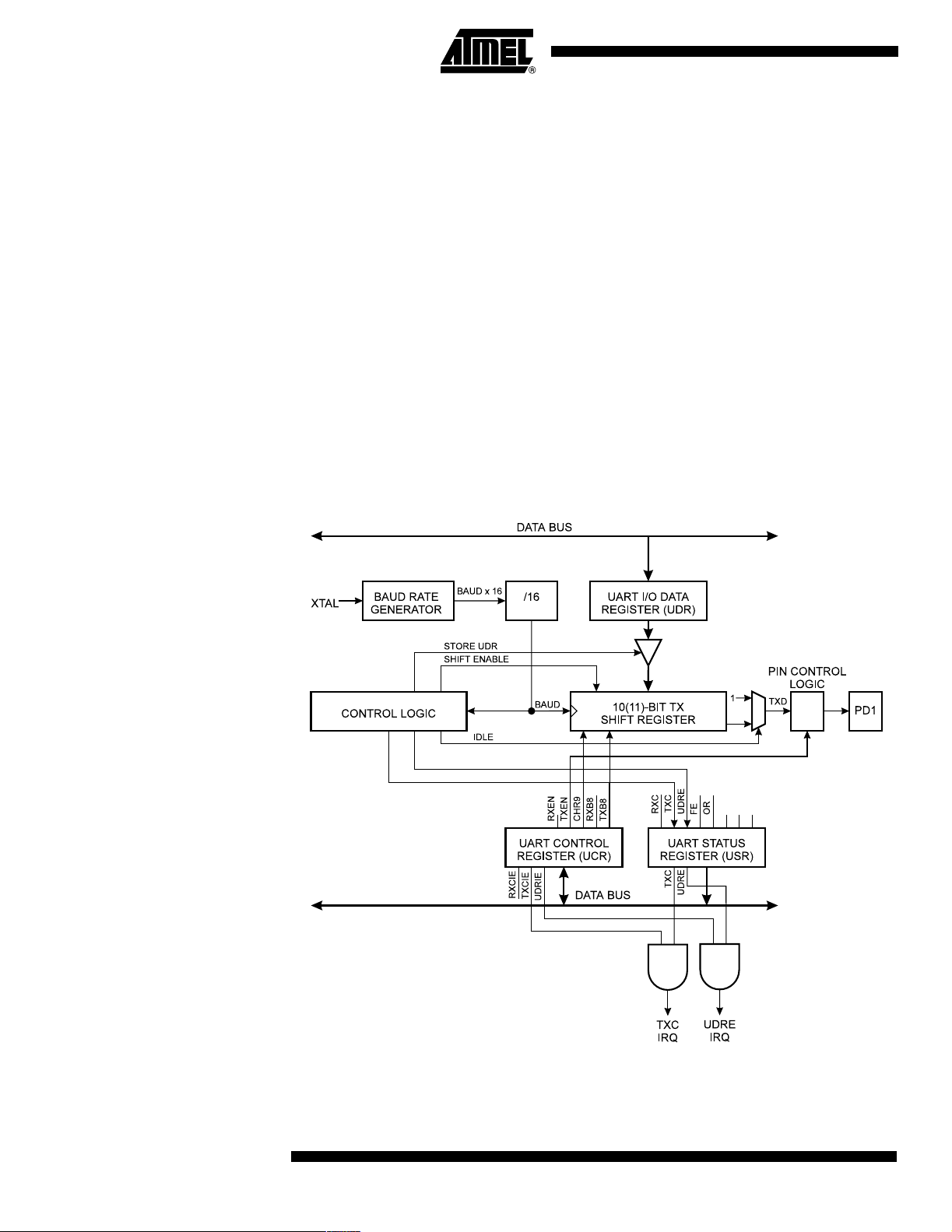
UART The AT90S2313 features a full duplex (separate Receive and Transmit Registers) Uni-
versal Asynchronous Receiver and Transmitter (UART). The main features are:
•
Baud Rate Generator that can Generate a Large Number of Baud Rates (bps)
• High Baud Rates at Low XTAL Frequencies
• 8 or 9 Bits Data
• Noise Filtering
• Overrun Detection
• Framing Error Detection
• False Start Bit Detection
• Three separate Interrupts on TX Complete, TX Data Register Empty and RX Complete
Data Transmission A block schematic of the UART transmitter is shown in Figure 34.
Data transmission is initiated by writing the data to be transmitted to the UART I/O Data
Register (UDR). Data is transferred from UDR to the Transmit Shift Register when:
• A new character has been written to UDR after the stop bit from the previous
character has been shifted out. The Shift Register is loaded immediately.
• A new character has been written to UDR before the stop bit from the previous
character has been shifted out. The Shift Register is loaded when the stop bit of the
character currently being transmitted has been shifted out.
Figure 34. UART Transmitter
42
If the 10(11)-bit Transmitter Shift Register is empty, data is transferred from UDR to the
Shift Register. At this time the UDRE (UART Data Register Empty) bit in the UART Sta-
AT90S2313
0839I–AVR–06/02
Page 43

tus Register (USR) is set. When this bit is set (one), the UART is ready to receive the
next character. At the same time as the data is transferred from UDR to the 10(11)-bit
Shift Register, bit 0 of the Shift Register is cleared (start bit) and bit 9 or 10 is set (stop
bit). If 9-bit data word is selected (the CHR9 bit in the UART Control Register [UCR] is
set), the TXB8 bit in UCR is transferred to bit 9 in the Transmit Shift Register.
On the Baud Rate clock following the transfer operation to the Shift Register, the start bit
is shifted out on the TXD pin. Then follows the data, LSB first. When the stop bit has
been shifted out, the Shift Register is loaded if any new data has been written to the
UDR during the transmission. During loading, UDRE is set. If there is no new data in the
UDR Register to send when the stop bit is shifted out, the UDRE Flag will remain set
until UDR is written again. When no new data has been written, and the stop bit has
been present on TXD for one bit length, the TX Complete Flag (TXC) in USR is set.
The TXEN bit in UCR enables the UART transmitter when set (one). When this bit is
cleared (zero), the PD1 pin can be used for general I/O. When TXEN is set, the UART
Transmitter will be connected to PD1, which is forced to be an output pin regardless of
the setting of the DDD1 bit in DDRD.
Data Reception Figure 35 shows a block diagram of the UART Receiver.
Figure 35. UART Receiver
AT90S2313
0839I–AVR–06/02
The Receiver front-end logic samples the signal on the RXD pin at a frequency of 16
times the baud rate. While the line is idle, one single sample of logical “0” will be interpreted as the falling edge of a start bit, and the start bit detection sequence is initiated.
Let sample 1 denote the first zero-sample. Following the 1-to-0 transition, the receiver
samples the RXD pin at samples 8, 9 and 10. If two or more of these three samples are
43
Page 44
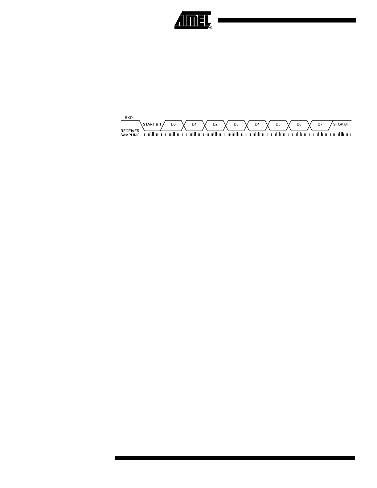
found to be logical “1”s, the start bit is rejected as a noise spike and the receiver starts
looking for the next 1-to-0 transition.
If, however, a valid start bit is detected, sampling of the data bits following the start bit is
performed. These bits are also sampled at samples 8, 9 and 10. The logical value found
in at least two of the three samples is taken as the bit value. All bits are shifted into the
Transmitter Shift Register as they are sampled. Sampling of an incoming character is
shown in Figure 36.
Figure 36. Sampling Received Data
When the stop bit enters the Receiver, the majority of the three samples must be “1” to
accept the stop bit. If two or more samples are logical “0”s, the Framing Error (FE) Flag
in the UART Status Register (USR) is set. Before reading the UDR Register, the user
should always check the FE bit to detect Framing Errors.
Whether or not a valid stop bit is detected at the end of a character-reception cycle, the
data is transferred to UDR and the RXC Flag in USR is set. UDR is in fact two physically
separate registers; one for transmitted data and one for received data. When UDR is
read, the Receive Data Register is accessed, and when UDR is written, the Transmit
Data Register is accessed. If 9-bit data word is selected (the CHR9 bit in the UART Control Register [UCR] is set), the RXB8 bit in UCR is loaded with bit 9 in the Transmit Shift
Register when data is transferred to UDR.
If, after having received a character, the UDR Register has not been read since the last
receive, the OverRun (OR) Flag in UCR is set. This means that the last data byte shifted
into the Shift Register could not be transferred to UDR and has been lost. The OR bit is
buffered and is updated when the valid data byte in UDR is read. Thus, the user should
always check the OR bit after reading the UDR Register in order to detect any overruns
if the baud rate is high or CPU load is high.
When the RXEN bit in the UCR Register is cleared (zero), the receiver is disabled. This
means that the PD0 pin can be used as a general I/O pin. When RXEN is set, the UART
Receiver will be connected to PD0, which is forced to be an input pin regardless of the
setting of the DDD0 bit in DDRD. When PD0 is forced to input by the UART, the
PORTD0 bit can still be used to control the pull-up resistor on the pin.
When the CHR9 bit in the UCR Register is set, transmitted and received characters are
nine bits long plus start and stop bits. The ninth data bit to be transmitted is the TXB8 bit
in UCR Register. This bit must be set to the wanted value before a transmission is initiated by writing to the UDR Register. The ninth data bit received is the RXB8 bit in the
UCR Register.
44
AT90S2313
0839I–AVR–06/02
Page 45
UART Control
The UART I/O Data Register – UDR
UART Status Register – USR
AT90S2313
Bit 76543210
$0C ($2C) MSB LSB UDR
Read/Write R/W R/W R/W R/W R/W R/W R/W R/W
Initialvalue00000000
The UDR Register is actually two physically separate registers sharing the same I/O
address. When writing to the register, the UART Transmit Data Register is written.
When reading from UDR, the UART Receive Data Register is read.
Bit 76543210
$0B ($2B) RXC TXC UDRE FE OR –––USR
Read/Write R R/W RRRRRR
Initialvalue00100000
The USR Register is a read-only register providing information on the UART status.
• Bit 7 – RXC: UART Receive Complete
This bit is set (one) when a received character is transferred from the Receiver Shift
Register to UDR. The bit is set regardless of any detected framing errors. When the
RXCIE bit in UCR is set, the UART Receive Complete interrupt will be executed when
RXC is set (one). RXC is cleared by reading UDR. When interrupt-driven data reception
is used, the UART Receive Complete Interrupt routine must read UDR in order to clear
RXC, otherwise a new interrupt will occur once the interrupt routine terminates.
• Bit 6 – TXC: UART Transmit Complete
This bit is set (one) when the entire character (including the stop bit) in the Transmit
Shift Register has been shifted out and no new data has been written to UDR. This flag
is especially useful in half-duplex communications interfaces, where a transmitting application must enter Receive mode and free the communications bus immediately after
completing the transmission.
When the TXCIE bit in UCR is set, setting of TXC causes the UART Transmit Complete
interrupt to be executed. TXC is cleared by hardware when executing the corresponding
interrupt handling vector. Alternatively, the TXC bit is cleared (zero) by writing a logical
“1” to the bit.
• Bit 5 – UDRE: UART Data Register Empty
This bit is set (one) when a character written to UDR is transferred to the Transmit Shift
Register. Setting of this bit indicates that the transmitter is ready to receive a new character for transmission.
When the UDRIE bit in UCR is set, the UART Transmit Complete interrupt is executed
as long as UDRE is set. UDRE is cleared by writing UDR. When interrupt-driven data
transmittal is used, the UART Data Register Empty Interrupt routine must write UDR in
order to clear UDRE, otherwise a new interrupt will occur once the interrupt routine
terminates.
0839I–AVR–06/02
UDRE is set (one) during reset to indicate that the transmitter is ready.
45
Page 46

UART Control Register – UCR
• Bit 4 – FE: Framing Error
This bit is set if a Framing Error condition is detected (i.e., when the stop bit of an incoming character is zero).
The FE bit is cleared when the stop bit of received data is one.
• Bit 3 – OR: OverRun
This bit is set if an OverRun condition is detected (i.e., when a character already present
in the UDR Register is not read before the next character has been shifted into the
Receiver Shift Register). The OR bit is buffered, which means that it will be set once the
valid data still in UDRE is read.
The OR bit is cleared (zero) when data is received and transferred to UDR.
• Bits 2..0 – Res: Reserved Bits
These bits are reserved bits in the AT90S2313 and will always read as zero.
Bit 76543210
$0A ($2A) RXCIE TXCIE UDRIE RXEN TXEN CHR9 RXB8 TXB8 UCR
Read/Write R/W R/W R/W R/W R/W R/W R W
Initialvalue00000010
• Bit 7 – RXCIE: RX Complete Interrupt Enable
When this bit is set (one), a setting of the RXC bit in USR will cause the Receive Complete Interrupt routine to be executed provided that global interrupts are enabled.
• Bit 6 – TXCIE: TX Complete Interrupt Enable
When this bit is set (one), a setting of the TXC bit in USR will cause the Transmit Complete Interrupt routine to be executed provided that global interrupts are enabled.
• Bit 5 – UDRIE: UART Data Register Empty Interrupt Enable
When this bit is set (one), a setting of the UDRE bit in USR will cause the UART Data
Register Empty Interrupt routine to be executed provided that global interrupts are
enabled.
• Bit 4 – RXEN: Receiver Enable
This bit enables the UART Receiver when set (one). When the Receiver is disabled, the
RXC, OR and FE Status Flags cannot become set. If these flags are set, turning off
RXEN does not cause them to be cleared.
• Bit 3 – TXEN: Transmitter Enable
This bit enables the UART Transmitter when set (one). When disabling the Transmitter
while transmitting a character, the Transmitter is not disabled before the character in the
Shift Register plus any following character in UDR has been completely transmitted.
• Bit 2 – CHR9: 9 Bit Characters
46
When this bit is set (one), transmitted and received characters are nine bits long plus
start and stop bits. The ninth bit is read and written by using the RXB8 and TXB8 bits in
UCR, respectively. The ninth data bit can be used as an extra stop bit or a parity bit.
AT90S2313
0839I–AVR–06/02
Page 47
AT90S2313
• Bit 1 – RXB8: Receive Data Bit 8
When CHR9 is set (one), RXB8 is the ninth data bit of the received character.
• Bit 0 – TXB8: Transmit Data Bit 8
When CHR9 is set (one), TXB8 is the ninth data bit in the character to be transmitted.
Baud Rate Generator The baud rate generator is a frequency divider that generates baud rates according to
the following equation:
f
BAUD
• BAUD = Baud Rate
• fCK= Crystal Clock frequency
• UBRR = Contents of the UART Baud Rate Register (UBRR) (0 - 255)
For standard crystal frequencies, the most commonly used baud rates can be generated
by using the UBRR settings in Table 15. UBRR values that yield an actual baud rate differing less than 2% from the target baud rate, are boldfaced in the table. However, using
baud rates that have more than 1% error is not recommended. High error ratings give
less noise resistance.
CK
-------------------------------------=
16(UBRR 1)+
Table 15. UBRR Settings at Various Crystal Frequencies
Baud Rate
2400
4800
9600
14400
19200
28800
38400
57600
76800
115200
Baud Rate
2400
4800
9600
14400
19200
28800
38400
57600
76800
115200
Baud Rate
2400
4800
9600
14400
19200
28800
38400
57600
76800
115200
UBRR=
UBRR=
UBRR= 6 7. 5 UBRR=
UBRR= 3 7. 8 UBRR=
UBRR= 2 7. 8 UBRR=
UBRR= 1 7. 8 UBRR=
UBRR= 1 22. 9 UBRR=
UBRR= 0 7. 8 UBRR=
UBRR= 0 22. 9 UBRR= 1 33.3 UBRR= 1 22. 9 UBRR=
UBRR= 0 84. 3 UBRR=
3.2768 MHz
UBRR=
UBRR=
UBRR=
UBRR=
UBRR= 10 3.1 UBRR=
UBRR=
UBRR= 4 6. 3 UBRR=
UBRR= 3 12. 5 UBRR=
UBRR= 2 12. 5 UBRR=
UBRR= 1 12. 5 UBRR=
7.3728 MHz
UBRR=
UBRR=
UBRR=
UBRR=
UBRR=
UBRR=
UBRR=
UBRR=
UBRR=
UBRR=
1MHz
25 0. 2
12 0. 2
84 0. 4
42 0. 8
20 1. 6
13 1. 6
191 0.0
95 0. 0
47 0. 0
31 0. 0
23 0. 0
15 0. 0
11 0. 0
%E rror
%E rror
61.6
%E rror
70.0
50.0
30.0
1.8432 MHz
UBRR=
UBRR=
3.6864 MHz
UBRR=
UBRR=
UBRR=
UBRR=
UBRR=
UBRR=
UBRR=
UBRR=
UBRR=
UBRR=
UBRR= 16 2.1 UBRR=
UBRR=
UBRR= 8 3. 7 UBRR=
UBRR= 6 7. 5 UBRR= 7 6.7 UB RR=
UBRR= 3 7. 8 UBRR=
47 0. 0
23 0. 0
11 0. 0
95 0. 0
47 0. 0
23 0. 0
15 0. 0
11 0. 0
8MHz
207 0.2
103 0.2
51 0. 2
34 0. 8
25 0. 2
12 0. 2
%E rror
UBRR=
UBRR=
UBRR=
70.0
50.0
30.0
20.0
10.0
00.0
70.0
50.0
30.0
20.0
10.0
UBRR= 8 3. 7 UBRR= 10 3.1
UBRR= 6 7. 5 UBRR=
UBRR= 3 7. 8 UBRR= 4 6.3
UBRR= 2 7. 8 UBRR=
UBRR= 1 7. 8 UBRR= 2 12.5
UBRR= 0 7. 8 UBRR= 0 25.0
%E rror
UBRR=
UBRR=
UBRR=
UBRR= 16 2.1 UBRR=
UBRR=
UBRR= 8 3. 7 UBRR=
UBRR= 6 7. 5 UBRR= 7 6.7
UBRR= 3 7. 8 UBRR=
UBRR= 2 7. 8 UBRR= 3 6.7
UBRR= 1 7. 8 UBRR= 2 20.0
%E rror
UBRR=
UBRR=
UBRR=
UBRR=
UBRR=
UBRR=
2MHz
4MHz
9.216 M Hz
%E rror
51 0. 2
25 0. 2
12 0. 2
%E rror
103 0.2
51 0. 2
25 0. 2
12 0. 2
%E rror
239 0.0
119 0.0
59 0. 0
39 0. 0
29 0. 0
19 0. 0
14 0. 0
90.0
40.0
2.4576 MHz
UBRR=
UBRR=
UBRR=
4.608 M Hz
UBRR=
UBRR=
UBRR=
UBRR=
11.059 MHz
UBRR= 287 UBRR=
UBRR=
UBRR=
UBRR=
UBRR=
UBRR=
UBRR=
UBRR=
%E rror
63 0. 0
31 0. 0
15 0. 0
70.0
30.0
10.0
%E rror
119 0.0
59 0. 0
29 0. 0
19 0. 0
14 0. 0
90.0
40.0
%E rror
143 0.0
71 0. 0
47 0. 0
35 0. 0
23 0. 0
17 0. 0
11 0. 0
80.0
50.0
0839I–AVR–06/02
47
Page 48

UART Baud Rate Register – UBRR
Bit 76543210
$09 ($29) MSB LSB UBRR
Read/Write R/W R/W R/W R/W R/W R/W R/W R/W
Initialvalue00000000
The UBRR Register is an 8-bit read/write register that specifies the UART Baud Rate
according to the formula on the previous page.
Analog Comparator The Analog Comparator compares the input values on the positive input AIN0 (PB0) and
the negative input PB1(AIN1). When the voltage on the positive input PB0 (AIN0) is
higher than the voltage on the negative input PB1 (AIN1), the Analog Comparator Output, ACO is set (one). The comparator’s output can be set to trigger the Timer/Counter1
Input Capture function. In addition, the comparator can trigger a separate interrupt
exclusive to the Analog Comparator. The user can select interrupt triggering on comparator output rise, fall or toggle. A block diagram of the comparator and its surrounding
logic is shown in Figure 37.
Figure 37. Analog Comparator Block Diagram
Analog Comparator Control and Status Register – ACSR
48
AT90S2313
Bit 76543210
$08 ($28) ACD – ACO ACI ACIE ACIC ACIS1 ACIS0 ACSR
Read/Write R/W R R R/W R/W R/W R/W R/W
Initialvalue00N/A00000
• Bit 7 – ACD: Analog Comparator Disable
When this bit is set (one), the power to the Analog Comparator is switched off. This bit
can be set at any time to turn off the Analog Comparator. This will reduce power consumption in active and Idle modes. When changing the ACD bit, the Analog Comparator
Interrupt must be disabled by clearing the ACIE bit in ACSR. Otherwise an interrupt can
occur when the bit is changed.
• Bit 6 – Res: Reserved Bit
This bit is a reserved bit in the AT90S2313 and will always read as zero.
0839I–AVR–06/02
Page 49
AT90S2313
• Bit 5 – ACO: Analog Comparator Output
ACO is directly connected to the comparator output.
• Bit 4 – ACI: Analog Comparator Interrupt Flag
This bit is set (one) when a comparator output event triggers the interrupt mode defined
by ACIS1 and ACIS0. The Analog Comparator Interrupt routine is executed if the ACIE
bit is set (one) and the I-bit in SREG is set (one). ACI is cleared by hardware when executing the corresponding interrupt handling vector. Alternatively, ACI is cleared by
writing a logical “1” to the flag. Observe, however, that if another bit in this register is
modified using the SBI or CBI instruction, ACI will be cleared if it has become set before
the operation.
• Bit 3 – ACIE: Analog Comparator Interrupt Enable
When the ACIE bit is set (one) and the I-bit in the Status Register is set (one), the Analog Comparator interrupt is activated. When cleared (zero), the interrupt is disabled.
• Bit 2 – ACIC: Analog Comparator Input Capture Enable
When set (one), this bit enables the Input Capture function in Timer/Counter1 to be triggered by the Analog Comparator. The comparator output is, in this case, directly
connected to the Input Capture front-end logic, making the comparator utilize the noise
canceler and edge-select features of the Timer/Counter1 Input Capture interrupt. When
cleared (zero), no connection between the Analog Comparator and the Input Capture
function is given. To make the comparator trigger the Timer/Counter1 Input Capture
interrupt, the TICIE1 bit in the Timer Interrupt Mask Register (TIMSK) must be set (one).
• Bits 1,0 – ACIS1, ACIS0: Analog Comparator Interrupt Mode Select
These bits determine which comparator events trigger the Analog Comparator interrupt.
The different settings are shown in Table 16.
Table 16. ACIS1/ACIS0 Settings
ACIS1 ACIS0 Interrupt Mode
0 0 Comparator Interrupt on Output Toggle
01Reserved
1 0 Comparator Interrupt on Falling Output Edge
1 1 Comparator Interrupt on Rising Output Edge
Note: 1. When changing the ACIS1/ACIS0 bits, the Analog Comparator Interrupt must be dis-
abled by clearing its Interrupt Enable bit in the ACSR Register. Otherwise an interrupt
can occur when the bits are changed.
(1)
0839I–AVR–06/02
49
Page 50

I/O Ports All AVR ports have true Read-Modify-Write functionality when used as general digital
I/O ports. This means that the direction of one port pin can be changed without unintentionally changing the direction of any other pin with the SBI and CBI instructions. The
same applies for changing drive value (if configured as output) or enabling/disabling of
pull-up resistors (if configured as input).
Port B Port B is an 8-bit bi-directional I/O port.
Three I/O memory address locations are allocated for the Port B, one each for the Data
Register – PORTB, $18 ($38), Data Direction Register – DDRB, $17($37) and the Port
B Input Pins – PINB, $16($36). The Port B Input Pins address is read-only, while the
Data Register and the Data Direction Register are read/write.
All port pins have individually selectable pull-up resistors. The Port B output buffers can
sink 20 mA and thus drive LED displays directly. When pins PB0 to PB7 are used as
inputs and are externally pulled low, they will source current if the internal pull-up resistors are activated.
The Port B pins with alternate functions are shown in Table 17.
Table 17. Port B Pin Alternate Functions
Port Pin Alternate Functions
PB0 AIN0 (Analog Comparator positive input)
PB1 AIN1 (Analog Comparator negative input)
Port B Data Register – PORTB
Port B Data Direction Register – DDRB
Port B Input Pins Address – PINB
PB3 OC1 (Timer/Counter1 Output Compare Match output)
PB5 MOSI (Data input line for memory downloading)
PB6 MISO (Data output line for memory uploading)
PB7 SCK (Serial clock input)
When the pins are used for the alternate function, the DDRB and PORTB Registers
have to be set according to the alternate function description.
Bit 76543210
$18 ($38)
Read/Write R/W R/W R/W R/W R/W R/W R/W R/W
Initialvalue00000000
Bit 76543210
$17 ($37) DDB7 DDB6 DDB5 DDB4 DDB3 DDB2 DDB1 DDB0 DDRB
Read/Write R/W R/W R/W R/W R/W R/W R/W R/W
Initialvalue00000000
Bit 76543210
$16 ($36) PINB7 PINB6 PINB5 PINB4 PINB3 PINB2 PINB1 PINB0 PINB
Read/Write R R R RRRRR
Initial value N/A N/A N/A N/A N/A N/A N/A N/A
PORTB7 PORTB6 PORTB5 PORTB4 PORTB3 PORTB2 PORTB1 PORTB0 PORTB
50
AT90S2313
0839I–AVR–06/02
Page 51
AT90S2313
The Port B Input Pins address (PINB) is not a register; this address enables access to
the physical value on each Port B pin. When reading PORTB, the Port B Data Latch is
read, and when reading PINB, the logical values present on the pins are read.
Port B as General Digital I/O All eight pins in Port B have equal functionality when used as digital I/O pins.
PBn, general I/O pin: The DDBn bit in the DDRB Register selects the direction of this
pin. If DDBn is set (one), PBn is configured as an output pin. If DDBn is cleared (zero),
PBn is configured as an input pin. If PORTBn is set (one) when the pin is configured as
an input pin, the MOS pull-up resistor is activated. To switch the pull-up resistor off, the
PORTBn has to be cleared (zero) or the pin has to be configured as an output pin The
Port B pins are tri-stated when a reset condition becomes active, even if the clock is not
active.
Table 18. DDBn Effects on Port B Pins
DDBn PORTBn I/O Pull-up Comment
0 0 Input No Tri-state (High-Z)
0 1 Input Yes PBn will source current if ext. pulled low
1 0 Output No Push-pull Zero Output
1 1 Output No Push-pull One Output
Note: 1. n:7,6…0, pin number.
Alternate Functions of Port B The alternate pin functions of Port B are:
• SCK – Port B, Bit 7
SCK, Clock Input pin for memory up/downloading.
• MISO – Port B, Bit 6
MISO, Data Output pin for memory uploading.
• MOSI – Port B, Bit 5
MOSI, Data Input pin for memory downloading.
• OC1 – Port B, Bit 3
(1)
0839I–AVR–06/02
OC1, Output Compare Match Output. The PB3 pin can serve as an external output for
Timer1 Compare Match. The PB3 pin has to be configured as an output (DDB3 is set
[one]) to serve this function. See the timer description for further details, and how to
enable the output.
• AIN1 – Port B, Bit 1
AIN1, Analog Comparator Negative Input. When configured as an input (DDB1 is
cleared [zero]) and with the internal MOS pull-up resistor switched off (PB1 is cleared
[zero]), this pin also serves as the negative input of the On-chip Analog Comparator.
• AIN0 – Port B, Bit 0
AIN0, Analog Comparator Positive Input. When configured as an input (DDB0 is cleared
[zero]) and with the internal MOS pull-up resistor switched off (PB0 is cleared [zero]),
this pin also serves as the positive input of the On-chip Analog Comparator.
51
Page 52

Port B Schematics Note that all port pins are synchronized. The synchronization latches are, however, not
shown in the figures.
Figure 38. Port B Schematic Diagram (Pins PB0 and PB1)
52
AT90S2313
0839I–AVR–06/02
Page 53

Figure 39. Port B Schematic Diagram (Pin PB3)
MOS
PULLUP
PB3
AT90S2313
RD
RESET
R
Q
D
DDB3
C
WD
RESET
R
Q
D
PORTB3
C
RL
RP
WP
DATA BUS
WP: WRITE PORTB
WD: WRITE DDRB
RL: READ PORTB LATCH
RP: READ PORTB PIN
RD: READ DDRB
OUTPUT
MODE SELECT
Figure 40. Port B Schematic Diagram (Pins PB2 and PB4)
COM1A0
COM1A1
COMP. MATCH1
0839I–AVR–06/02
53
Page 54
Figure 41. Port B Schematic Diagram (Pin PB5)
Figure 42. Port B Schematic Diagram (Pin PB6)
54
AT90S2313
0839I–AVR–06/02
Page 55

Figure 43. Port B Schematic Diagram (Pin PB7)
AT90S2313
Port D Three I/O memory address locations are allocated for the Port D: one each for the Data
Register – PORTD, $12($32), Data Direction Register – DDRD, $11($31) and the Port D
Input Pins – PIND, $10($30). The Port D Input Pins address is read-only, while the Data
Register and the Data Direction Register are read/write.
Port D has seven bi-directional I/O pins with internal pull-up resistors, PD6..PD0. The
Port D output buffers can sink 20 mA. As inputs, Port D pins that are externally pulled
low will source current if the pull-up resistors are activated.
Some Port D pins have alternate functions as shown in Table 19:
Table 19. Port D Pin Alternate Functions
Port Pin Alternate Function
PD0 RXD (Receive data input for the UART)
PD1 TXD (Transmit data output for the UART)
PD2 INT0 (External interrupt 0 input)
PD3 INT1 (External interrupt 1 input)
PD4 TO (Timer/Counter0 external input)
PD5 T1 (Timer/Counter1 external input)
PD6 ICP (Timer/Counter1Input Capture pin)
When the pins are used for the alternate function, the DDRD and PORTD Registers
have to be set according to the alternate function description.
0839I–AVR–06/02
55
Page 56

Port D Data Register – PORTD
Bit 76543210
$12 ($32)
Read/Write R R/W R/W R/W R/W R/W R/W R/W
Initialvalue00000000
– PORTD6 PORTD5 PORTD4 PORTD3 PORTD2 PORTD1 PORTD0 PORTD
Port D Data Direction Register – DDRD
Bit 76543210
$11 ($31) – DDD6 DDD5 DDD4 DDD3 DDD2 DDD1 DDD0 DDRD
Read/Write R R/W R/W R/W R/W R/W R/W R/W
Initialvalue00000000
Port D Input Pins Address – PIND
Bit 76543210
$10 ($30) – PIND6 PIND5 PIND4 PIND3 PIND2 PIND1 PIND0 PIND
Read/Write R R R RRRRR
Initial value 0 N/A N/A N/A N/A N/A N/A N/A
The Port D Input Pins address (PIND) is not a register; this address enables access to
the physical value on each Port D pin. When reading PORTD, the Port D Data Latch is
read, and when reading PIND, the logical values present on the pins are read.
Port D as General Digital I/O PDn, general I/O pin: The DDDn bit in the DDRD Register selects the direction of this
pin. If DDDn is set (one), PDn is configured as an output pin. If DDDn is cleared (zero),
PDn is configured as an input pin. If PORTDn is set (one) when configured as an input
pin, the MOS pull-up resistor is activated. To switch the pull-up resistor off, the PORTDn
has to be cleared (zero) or the pin has to be configured as an output pin. The Port D pins
are tri-stated when a reset condition becomes active, even if the clock is not active.
Table 20. DDDn Bits on Port D Pins
DDDn PORTDn I/O Pull-up Comment
0 0 Input No Tri-state (High-Z)
0 1 Input Yes PDn will source current if ext. pulled low
1 0 Output No Push-pull Zero Output
1 1 Output No Push-pull One Output
Note: 1. n: 6…0, pin number.
Alternate Functions of Port D The alternate functions of Port D are:
• ICP – Port D, Bit 6
Timer/Counter1 Input Capture pin. See the Timer/Counter1 description for further
details.
• T1 – Port D, Bit 5
T1, Timer 1 Clock source. See the Timer description for further details.
• T0 – Port D, Bit 4
T0, Timer/Counter0 Clock source. See the Timer description for further details.
(1)
56
AT90S2313
0839I–AVR–06/02
Page 57

AT90S2313
• INT1 – Port D, Bit 3
INT1, External Interrupt Source 1. The PD3 pin can serve as an external interrupt
source to the MCU. See the interrupt description for further details and how to enable
the source.
• INT0 – Port D, Bit 2
INT0, External Interrupt Source 0. The PD2 pin can serve as an external interrupt
source to the MCU. See the interrupt description for further details and how to enable
the source.
• TXD – Port D, Bit 1
Transmit Data (Data Output pin for the UART). When the UART Transmitter is enabled,
this pin is configured as an output regardless of the value of DDRD1.
• RXD – Port D, Bit 0
Receive Data (Data Input pin for the UART). When the UART Receiver is enabled, this
pin is configured as an input regardless of the value of DDRD0. When the UART forces
thispintobeaninput,alogical“1” in PORTD0 will turn on the internal pull-up.
Port D Schematics Note that all port pins are synchronized. The synchronization latches are, however, not
shown in the figures.
Figure 44. Port D Schematic Diagram (Pin PD0)
MOS
PULLUP
PD0
WRITE PORTD
WP:
WRITE DDRD
WD:
READ PORTD LATCH
RL:
READ PORTD PIN
RP:
READ DDRD
RD:
UART RECEIVE DATA
RXD:
UART RECEIVE ENABLE
RXEN:
RD
RESET
D
Q
DDD0
C
WD
RESET
D
Q
PORTD0
C
RL
RP
WP
RXEN
RXD
DATA BUS
0839I–AVR–06/02
57
Page 58

Figure 45. Port D Schematic Diagram (Pin PD1)
MOS
PULLUP
PD1
WRITE PORTD
WP:
WRITE DDRD
WD:
READ PORTD LATCH
RL:
READ PORTD PIN
RP:
READ DDRD
RD:
UART TRANSMIT DATA
TXD:
UART TRANSMIT ENABLE
TXEN:
RD
RESET
R
D
Q
DDD1
C
WD
RESET
R
Q
D
PORTD1
C
RL
RP
WP
DATA B US
TXEN
TXD
Figure 46. Port D Schematic Diagram (Pins PD2 and PD3)
58
AT90S2313
0839I–AVR–06/02
Page 59

Figure 47. Port D Schematic Diagram (Pins PD4 and PD5)
MOS
PULLUP
PDn
RL
RP
AT90S2313
RD
RESET
R
D
Q
DDDn
C
WD
RESET
R
Q
PORTDn
C
WP
D
DATA BUS
WRITE PORTD
WP:
WRITE DDRD
WD:
READ PORTD LATCH
RL:
READ PORTD PIN
RP:
READ DDRD
RD:
4, 5
n:
0, 1
m:
SENSE CONTROL
CSm2
CSm1
Figure 48. Port D Schematic Diagram (Pin PD6)
CSm0
TIMERm CLOCK
SOURCE MUX
0839I–AVR–06/02
59
Page 60
Memory Programming
Program and Data Memory Lock Bits
The AT90S2313 MCU provides two Lock bits that can be left unprogrammed (“1”)orcan
be programmed (“0”) to obtain the additional features listed in Table 21. The Lock bits
can only be erased with the Chip Erase operation.
Table 21. Lock Bit Protection Modes
Memory Lock Bits
Protection TypeMode LB1 LB2
1 1 1 No memory lock features enabled.
2 0 1 Further programming of the Flash and EEPROM is disabled.
3 0 0 Same as mode 2, and verify is also disabled.
Note: 1. In the Parallel mode, further programming of the Fuse bits are also disabled. Program
the Fuse bits before programming the Lock bits.
Fuse Bits The AT90S2313 has two Fuse bits: SPIEN and FSTRT.
• When the SPIEN Fuse is programmed (“0”), Serial Program and Data Downloading
is enabled. The default value is programmed (“0”).
• When the FSTRT Fuse is programmed (“0”), the short start-up time is selected. The
default value is unprogrammed (“1”). Parts with this bit pre-programmed (“0”)canbe
delivered on demand.
The Fuse bits are not accessible in Serial Programming mode. The status of the fuses
are not affected by Chip Erase.
(1)
Signature Bytes All Atmel microcontrollers have a 3-byte signature code that identifies the device. This
code can be read in both serial and parallel mode. The three bytes reside in a separate
address space.
(1)
they are:
Programming the Flash and EEPROM
For the AT90S2313
1. $000: $1E (indicates manufactured by Atmel).
2. $001: $91 (indicates 2 Kb Flash memory).
3. $002: $01 (indicates AT90S2313 device when signature byte $001 is $91).
Note: 1. When both Lock bits are programmed (Lock mode 3), the signature bytes cannot be
read in serial mode. Reading the signature bytes will return: $00, $01 and $02.
Atmel’s AT90S2313 offers 2K bytes of In-System Reprogrammable Flash Program
memory and 128 bytes of EEPROM Data memory.
The AT90S2313 is shipped with the On-chip Flash Program and EEPROM Data memory arrays in the erased state (i.e., contents = $FF) and ready to be programmed. This
device supports a high-voltage (12V) Parallel Programming mode and a low-voltage
Serial Programming mode. The +12V is used for programming enable only, and no current of significance is drawn by this pin. The Serial Programming mode provides a
convenient way to download program and data into the AT90S2313 inside the user’s
system.
The program and EEPROM memory arrays in the AT90S2313 are programmed byteby-byte in either programming mode. For the EEPROM, an auto-erase cycle is provided
60
AT90S2313
0839I–AVR–06/02
Page 61
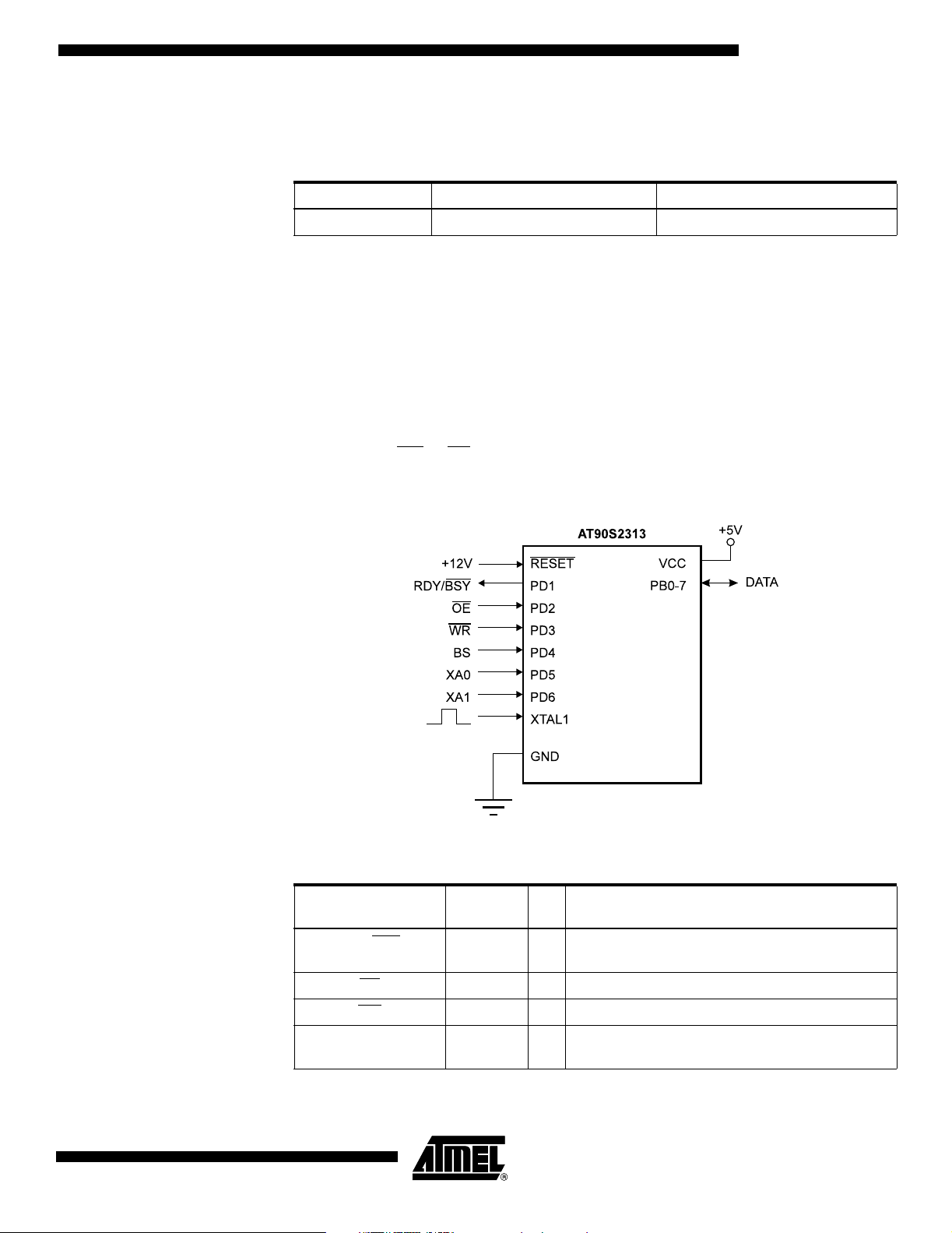
AT90S2313
within the self-timed write instruction in the Serial Programming mode. During programming, the supply voltage must be in accordance with Table 22.
Table 22. Supply Voltage during Programming
Part Serial Programming Parallel Programming
AT90S2313 2.7 - 6.0V 4.5 - 5.5V
Parallel Programming This section describes how to parallel program and verify Flash Program memory,
EEPROM data memory, Lock bits and Fuse bits in the AT90S2313.
Signal Names In this section, some pins of the AT90S2313 are referenced by signal names describing
their function during parallel programming. Pins not described in the following table are
referenced by pin names. See Figure 49 and Table 23. Pins not described in Table 23
are referenced by pin names.
The XA1/XA0 pins determine the action executed when the XTAL1 pin is given a positive pulse. The bit coding is shown in Table 24.
When pulsing WR
or OE, the command loaded determines the action executed. The
command is a byte where the different bits are assigned functions as shown in Table 25.
Figure 49. Parallel Programming
.
Table 23. Pin Name Mapping
Signal Name in
Programming Mode Pin Name I/O Function
0839I–AVR–06/02
RDY/BSY
OE
WR
BS PD4 I Byte Select (“0” selects low byte, “1” selects high
PD1 O 0: Device is busy programming, 1: Device is ready
for new command
PD2 I Output Enable (Active low)
PD3 I Write Pulse (Active low)
byte)
61
Page 62

Table 23. Pin Name Mapping
Signal Name in
Programming Mode Pin Name I/O Function
XA0 PD5 I XTAL Action Bit 0
XA1 PD6 I XTAL Action Bit 1
DATA PB7 - 0 I/O Bi-directional Data Bus (Output when OE
is low)
Table 24. XA1 and XA0 Coding
XA1 XA0 Action when XTAL1 is Pulsed
0 0 Load Flash or EEPROM Address (High or low address byte determined by BS)
0 1 Load Data (High or Low data byte for Flash determined by BS)
1 0 Load Command
1 1 No Action, Idle
Table 25. Command Byte Bit Coding
Command Byte Command Executed
1000 0000 Chip Erase
0100 0000 Write Fuse Bits
0010 0000 Write Lock Bits
0001 0000 Write Flash
0001 0001 Write EEPROM
0000 1000 Read Signature Bytes
0000 0100 Read Fuse and Lock Bits
0000 0010 Read Flash
0000 0011 Read EEPROM
Enter Programming Mode The following algorithm puts the device in Parallel Programming mode:
1. Apply supply voltage according to Table 22, between V
2. Set the RESET
3. Apply 11.5 - 12.5V to RESET
been applied to RESET
and BS pin to “0” and wait at least 100 ns.
. Any activity on BS within 100 ns after +12V has
, will cause the device to fail entering Programming
and GND.
CC
mode.
Chip Erase The Chip Erase command will erase the Flash and EEPROM memories, and the Lock
bits. The Lock bits are not reset until the Flash and EEPROM have been completely
erased. The Fuse bits are not changed. Chip Erase must be performed before the Flash
or EEPROM is reprogrammed.
Load Command “Chip Erase”
1. SetXA1,XA0to“10”. This enables command loading.
2. Set BS to “0”.
3. Set DATA to “1000 0000”. This is the command for Chip Erase.
4. Give XTAL1 a positive pulse. This loads the command.
62
AT90S2313
0839I–AVR–06/02
Page 63

AT90S2313
5. Give WR a t
for
t
WLWH_CE
WLWH_CE
value. Chip Erase does not generate any activity on the RDY/BSY
wide negative pulse to execute Chip Erase. See Table 26
pin.
Programming the Flash A: Load Command “Write Flash”
1. SetXA1,XA0to“10”. This enables command loading.
2. Set BS to “0”.
3. Set DATA to “0001 0000”. This is the command for Write Flash.
4. Give XTAL1 a positive pulse. This loads the command.
B: Load Address High Byte
1. SetXA1,XA0to“00”. This enables address loading.
2. Set BS to “1”. This selects high byte.
3. Set DATA = Address high byte ($00 - $03).
4. Give XTAL1 a positive pulse. This loads the address high byte.
C: Load Address Low Byte
1. SetXA1,XA0to“00”. This enables address loading.
2. Set BS to “0”. This selects low byte.
3. Set DATA = Address low byte ($00 - $FF).
4. Give XTAL1 a positive pulse. This loads the address low byte.
D: Load Data Low Byte
1. SetXA1,XA0to“01”. This enables data loading.
2. Set DATA = Data low byte ($00 - $FF).
3. Give XTAL1 a positive pulse. This loads the data low byte.
E: Write Data Low Byte
1. Set BS to “0”. This selects low data.
2. Give WR
a negative pulse. This starts programming of the data byte. RDY/BSY
goes low.
3. Wait until RDY/BSY
goes high to program the next byte.
(See Figure 50 for signal waveforms.)
F: Load Data High Byte
1. SetXA1,XA0to“01”. This enables data loading.
2. Set DATA = Data high byte ($00 - $FF).
3. Give XTAL1 a positive pulse. This loads the data high byte.
G:WriteDataHighByte
1. Set BS to “1”. This selects high data.
2. Give WR
a negative pulse. This starts programming of the data byte. RDY/BSY
goes low.
3. Wait until RDY/BSY
goes high to program the next byte.
(See Figure 51 for signal waveforms.)
0839I–AVR–06/02
63
Page 64

The loaded command and address are retained in the device during programming. For
efficient programming, the following should be considered:
• The command needs only be loaded once when writing or reading multiple memory
locations.
• Address high byte needs only be loaded before programming a new 256-word page
in the Flash.
• Skip writing the data value $FF; that is, the contents of the entire Flash and
EEPROM after a Chip Erase.
These considerations also apply to EEPROM programming and Flash, EEPROM and
signature byte reading.
Figure 50. Programming the Flash
$10 ADDR. HIGH ADDR. LOW DATA LOWDATA
XA1
XA0
BS
XTAL1
WR
RDY/BSY
RESET
12V
OE
Figure 51. Programming the Flash (Continued)
DATA
XA1
XA0
BS
XTAL1
WR
RDY/BSY
RESET
DATA HIGH
+12V
64
OE
AT90S2313
0839I–AVR–06/02
Page 65

AT90S2313
Reading the Flash The algorithm for reading the Flash memory is as follows (refer to “Programming the
Flash” for details on command and address loading):
1. A: Load Command “0000 0010”.
2. B: Load Address High Byte ($00 - $03).
3. C: Load Address Low Byte ($00 - $FF).
4. Set OE
5. Set BS to “1”. The Flash word high byte can now be read from DATA.
6. Set OE
Programming the EEPROM The programming algorithm for the EEPROM data memory is as follows (refer to “Pro-
gramming the Flash” for details on command, address and data loading):
1. A: Load Command “0001 0001”.
2. C: Load Address Low Byte ($00 - $7F).
3. D: Load Data Low Byte ($00 - $FF).
4. E: Write Data Low Byte.
Reading the EEPROM The algorithm for reading the EEPROM memory is as follows (refer to “Programming the
Flash” for details on command and address loading):
1. A: Load Command “0000 0011”.
2. C: Load Address Low Byte ($00 - $7F).
3. Set OE
4. Set OE
to “0”, and BS to “0”. The Flash word low byte can now be read at DATA.
to “1”.
to “0”, and BS to “0”. The EEPROM data byte can now be read at DATA.
to “1”.
Programming the Fuse Bits The algorithm for programming the Fuse bits is as follows (refer to “Programming the
Flash” for details on command and data loading):
1. A: Load Command “0100 0000”.
2. D: Load Data Low Byte. Bit n = “0” programs and bit n = “1” erases the Fuse bit.
Bit 5 = SPIEN Fuse bit.
Bit 0 = FSTRT Fuse bit.
Bit7-6,4-1=“1”. These bits are reserved and should be left unprogrammed (“1”).
3. Give WR
a t
WLWH_PFB
wide negative pulse to execute the programming; t
WLWH_PFB
is
found in Table 26. Programming the Fuse bits does not generate any activity on
the RDY/BSY
pin.
Programming the Lock Bits The algorithm for programming the Lock bits is as follows (refer to “Programming the
Flash” on page 63 for details on command and data loading):
1. A: Load Command “0010 0000”.
2. D: Load Data Low Byte. Bit n = “0” programs the Lock bit.
Bit 2 = Lock Bit2
Bit 1 = Lock Bit1
Bit7-3,0=“1”. These bits are reserved and should be left unprogrammed (“1”).
3. E: Write Data Low Byte.
The Lock bits can only be cleared by executing Chip Erase.
0839I–AVR–06/02
65
Page 66

Reading the Fuse and Lock Bits
Reading the Signature Bytes The algorithm for reading the signature bytes is as follows (refer to “Programming the
The algorithm for reading the Fuse and Lock bits is as follows (refer to “Programming
the Flash” on page 63 for details on command loading):
1. A: Load Command “0000 0100”.
2. Set OE
read at DATA (“0” means programmed).
Bit 7 = Lock Bit1
Bit 6 = Lock Bit2
Bit 5 = SPIEN Fuse bit
Bit 0 = FSTRT Fuse bit
3. Set OE
Observe that BS needs to be set to “1”.
Flash” on page 63 for details on command and address loading):
1. A: Load Command “0000 1000”.
2. C: Load Address Low Byte ($00 - $02).
Set OE
3. Set OE
to “0”, and BS to “1”. The status of the Fuse and Lock bits can now be
to “1”.
to “0”,andBSto“0”. The selected signature byte can now be read at DATA.
to “1”.
66
AT90S2313
0839I–AVR–06/02
Page 67

AT90S2313
Parallel Programming Characteristics
Figure 52. Parallel Programming Timing
t
XLWL
t
DVXH
t
XHXL
t
XLDX
t
BVWL
XTAL1
Data & Contol
(DATA, XA0/1, BS)
t
WR
WLWH
t
WHRL
t
RHBX
RDY/BSY
t
WLRH
OE
t
XLOL
t
OLDV
t
OHDZ
DATA
Table 26. Parallel Programming Characteristics, TA=25°C ± 10%, VCC= 5V ± 10%
Symbol Parameter Min Typ Max Units
V
PP
I
PP
t
DVX H
t
XHXL
t
XLDX
t
XLWL
t
BVWL
t
RHBX
t
WLWH
t
WHRL
t
WLRH
t
XLOL
t
OLDV
t
OHDZ
t
WLWH_CE
t
WLWH_PFB
Notes: 1. Use t
Programming Enable Voltage 11.5 12.5 V
Programming Enable Current 250.0 µA
Data and Control Setup before XTAL1 High 67.0 ns
XTAL1 Pulse Width High 67.0 ns
Data and Control Hold after XTAL1 Low 67.0 ns
XTAL1 Low to WR Low 67.0 ns
BSValidtoWRLow 67.0 ns
BS Hold after RDY/BSY High 67.0 ns
WR Pulse Width Low
WR High to RDY/BSY Low
WR Low to RDY/BSY High
(1)
(2)
(2)
67.0 ns
20.0 ns
0.5 0.7 0.9 ms
XTAL1 Low to OE Low 67.0 ns
OE Low to DATA Valid 20.0 ns
OE High to DATA Tri-stated 20.0 ns
WR Pulse Width Low for Chip Erase 5.0 10.0 15.0 ms
WR Pulse Width Low for Programming the Fuse
Bits 1.0 1.5 1.8 ms
2. If t
WLWH_CE
WLWH
forchiperaseandt
is held longer than t
WLWH_PFB
, no RDY/BSY pulse will be seen.
WLRH
for programming the Fuse bits.
Write
Read
0839I–AVR–06/02
67
Page 68
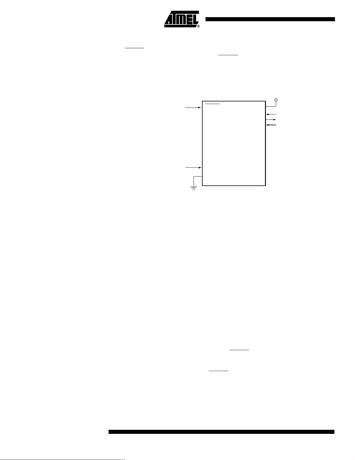
Serial Downloading Both the program and data memory arrays can be programmed using the serial SPI bus
while RESET
and MISO (output). See Figure 53. After RESET
instruction needs to be executed first before program/erase instructions can be
executed.
Figure 53. Serial Programming and Verify
is pulled to GND. The serial interface consists of pins SCK, MOSI (input)
is set low, the Programming Enable
AT90S2313
2.7 - 6.0V
VCC
PB7
PB6
PB5
SCK
MISO
MOSI
CLOCK INPUT
RESET
XTAL1
GND
For the EEPROM, an auto-erase cycle is provided within the self-timed write instruction
and there is no need to first execute the Chip Erase instruction. The Chip Erase instruction turns the content of every memory location in both the program and EEPROM
arrays into $FF.
The program and EEPROM memory arrays have separate address spaces: $0000 to
$03FF for program Flash memory and $000 to $07F for EEPROM data memory.
Either an external clock is supplied at pin XTAL1 or a crystal needs to be connected
across pins XTAL1 and XTAL2. The minimum low and high periods for the serial clock
(SCK) input are defined as follows:
Serial Programming Algorithm
68
AT90S2313
Low: > 2 XTAL1 clock cycle
High: > 2 XTAL1 clock cycles
When writing serial data to the AT90S2313, data is clocked on the rising edge of SCK.
When reading data from the AT90S2313, data is clocked on the falling edge of SCK.
See Figure 54, Figure and Table 29 for timing details.
To program and verify the AT90S2313 in the Serial Programming mode, the following
sequence is recommended (See 4-byte instruction formats in Table 28):
1. Power-up sequence:
Apply power between V
and GND while RESET and SCK are set to “0”.Ifacrys-
CC
tal is not connected across pins XTAL1 and XTAL2, apply a clock signal to the
XTAL1 pin. In some systems, the programmer cannot guarantee that SCK is held
low during Power-up. In this case, RESET
must be given a positive pulse of at least
two XTAL1 cycles duration after SCK has been set to “0”.
2. Wait for at least 20 ms and enable serial programming by sending the Programming Enable serial instruction to the MOSI (PB5) pin.
3. The serial programming instructions will not work if the communication is out of
synchronization. When in sync, the second byte ($53) will echo back when issu-
0839I–AVR–06/02
Page 69

AT90S2313
ing the third byte of the Programming Enable instruction. Whether the echo is
correct or not, all four bytes of the instruction must be transmitted. If the $53 did
not echo back, give SCK a positive pulse and issue a new Programming Enable
instruction. If the $53 is not seen within 32 attempts, there is no functional device
connected.
4. If a Chip Erase is performed (must be done to erase the Flash), wait t
after the instruction, give RESET a positive pulse, and start over from step 2.
See Table 30 for t
WD_ERASE
value.
5. The Flash or EEPROM array is programmed one byte at a time by supplying the
address and data together with the appropriate Write instruction. An EEPROM
memory location is first automatically erased before new data is written. Use
Data Polling to detect when the next byte in the Flash or EEPROM can be written. If polling is not used, wait t
See Table 31 for t
WD_PROG
value. In an erased device, no $FFs in the data file(s)
WD_PROG
before transmitting the next instruction.
need to be programmed.
6. Any memory location can be verified by using the Read instruction that returns
the content at the selected address at the serial output MISO (PB6) pin.
7. At the end of the programming session, RESET
can be set high to commence
normal operation.
8. Power-off sequence (if needed):
Set XTAL1 to “0” (if a crystal is not used).
power off.
CC
to “1”.
Set RESET
Turn V
WD_ERASE
Data Polling EEPROM When a byte is being programmed into the EEPROM, reading the address location
being programmed will give the value P1 until the auto-erase is finished, and then the
value P2. See Table 27 for P1 and P2 values.
At the time the device is ready for a new EEPROM byte, the programmed value will read
correctly. This is used to determine when the next byte can be written. This will not work
for the values P1 and P2, so when programming these values, the user will have to wait
for at least the prescribed time t
30 for t
WD_PROG
value. As a chip-erased device contains $FF in all locations, program-
WD_PROG
before programming the next byte. See Table
ming of addresses that are meant to contain $FF can be skipped. This does not apply if
the EEPROM is reprogrammed without first chip-erasing the device.
Table 27. Read Back Value during EEPROM Polling
Part P1 P2
AT90S2313 $80 $7F
0839I–AVR–06/02
69
Page 70
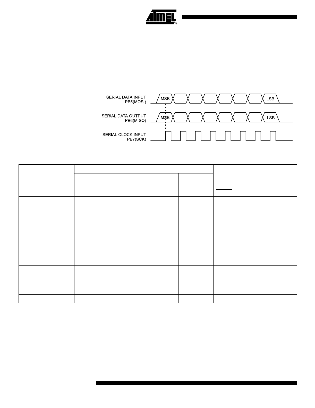
Data Polling Flash When a byte is being programmed into the Flash, reading the address location being
programmed will give the value $7F. At the time the device is ready for a new byte, the
programmed value will read correctly. This is used to determine when the next byte can
be written. This will not work for the value $7F, so when programming this value, the
user will have to wait for at least t
WD_PROG
before programming the next byte. As a chiperased device contains $FF in all locations, programming of addresses that are meant
to contain $FF can be skipped.
Figure 54. Serial Programming Waveforms
Table 2 8. Serial Programming Instruction Set
Instruction Format
Instruction
Programming Enable
Chip Erase
Read Program Memory
Write Program Memory
Read EEPROM
Memory
Write EEPROM
Memory
Write Lock Bits
Read Signature Bytes 0011 0000 xxxx xxxx xxxx xxbb oooo oooo Read signature byte o at address b.
Note: a = address high bits, b = address low bits, H =0– Low byte, 1 – High Byte, o = data out, i = data in, x = don’t care,1= Lock bit
1,
2
= Lock bit 2.
Note: 1. The signature bytes are not readable in lock mode 3, i.e. both Lock bits programmed.
1010 1100 0101 0011 xxxx xxxx xxxx xxxx Enable serial programming while
1010 1100 100x xxxx xxxx xxxx xxxx xxxx Chip erase Flash and EEPROM
0010 H000 xxxx xxaa bbbb bbb b oooo oooo Read H (highorlow)datao from
0100 H000 xxxx xxaa bbbb bbb b iiii iiii Write H (high or low) data i to
1010 0000 xxxx xxxx xbbb bbbb oooo oooo Read data o from EEPROM memory
1100 0000 xxxx xxxx xbbb bbbb iiii iiii Write data i to EEPROM memory at
1010 1100 111x x
21
x xxxx xxxx xxxx xxxx Write Lock bits. Set bits
OperationByte 1 Byte 2 Byte 3 Byte4
RESET
memory arrays.
program memory at word address
a:b.
program memory at word address
a:b.
at address b.
address b.
program Lock bits.
is low.
1,2
= “0” to
(1)
70
AT90S2313
0839I–AVR–06/02
Page 71

AT90S2313
Serial Programming Characteristics
Figure 55. Serial Programming Timing
MOSI
SCK
MISO
t
OVSH
t
SHSL
t
SHOX
Tabl e 29. Serial Programming Characteristics, T
t
SLSH
t
SLIV
=-40°Cto85°C, VCC=2.7-6.0V
A
(unless otherwise noted)
Symbol Parameter Min Typ Max Units
1/t
t
CLCL
1/t
t
CLCL
t
SHSL
t
SLSH
t
OVSH
t
SHOX
t
SLIV
CLCL
CLCL
Oscillator Frequency (VCC= 2.7 - 6.0V) 0 4.0 MHz
Oscillator Period (VCC= 2.7 - 6.0V) 250.0 ns
Oscillator Frequency (VCC=4.0-6.0V) 0 10.0 MHz
Oscillator Period (VCC= 4.0 - 6.0V) 100.0 ns
SCK Pulse Width High 2.0 t
SCK Pulse Width Low 2.0 t
MOSI Setup to SCK High t
MOSI Hold after SCK High 2.0 t
CLCL
CLCL
CLCL
CLCL
SCK Low to MISO Valid 10.0 16.0 32.0 ns
ns
ns
ns
ns
Table 30. Minimum Wait Delay after the Chip Erase Instruction
Symbol 3.2V 3.6V 4.0V 5.0V
t
WD_ERASE
18 ms 14 ms 12 ms 8 ms
Table 31. Minimum Wait Delay after Writing a Flash or EEPROM Location
Symbol 3.2V 3.6V 4.0V 5.0V
t
WD_PROG
9ms 7ms 6ms 4ms
0839I–AVR–06/02
71
Page 72

Electrical Characteristics
Absolute Maximum Ratings*
Operating Temperature .................................. -55°Cto+125°C
Storage Temperature ..................................... -65°Cto+150°C
Voltage on Any Pin Except RESET
with Respect to Ground ...............................-1.0V to VCC+0.5V
Voltage on RESET
Maximum Operating Voltage ............................................ 6.6V
DC Current per I/O Pin ............................................... 40.0 mA
with Respect to Ground ....-1.0V to +13.0V
*NOTICE: Stresses beyond those listed under “Absolute
Maximum Ratings” may cause permanent dam-
age to the device. This is a stress rating only and
functional operation of the device at these or
other conditions beyond those indicated in the
operational sections of this specification is not
implied. Exposure to absolute maximum rating
conditions for extended periods may affect device
reliability.
DC Current V
and GND Pins ................................ 200.0 mA
CC
DC Characteristics
TA=-40°Cto85°C, VCC= 2.7V to 6.0V (unless otherwise noted)
Symbol Parameter Condition Min Typ Max Units
V
IL
V
IL1
V
IH
V
IH1
V
IH2
V
OL
V
OH
I
IL
I
IH
Input Low Voltage (Except XTAL1) -0.5 0.3 V
Input Low Voltage (XTAL1) -0.5 0.3 V
4.3
2.3
CC
CC
CC
(2)
(2)
(2)
Input High Voltage (Except XTAL1, RESET)0.6V
Input High Voltage (XTAL1) 0.7 V
Input High Voltage (RESET)0.85V
Output Low Voltage
(Ports B, D)
Output High Voltage
(Ports B, D)
Input Leakage
Current I/O pin
Input Leakage
Current I/O pin
(3)
(4)
=20mA,VCC=5V
I
OL
I
=10mA,VCC=3V
OL
=-3mA,VCC=5V
I
OH
I
=-1.5mA,VCC=3V
OH
VCC= 6V, pin low
(absolute value)
VCC=6V,pinhigh
(absolute value)
RRST Reset Pull-up Resistor 100.0 500.0 kΩ
(1)
CC
(1)
CC
VCC+0.5 V
VCC+0.5 V
VCC+0.5 V
0.6
0.5
1.5 µA
980.0 nA
V
V
V
V
V
V
72
R
I/O
I
CC
I
CC
V
ACI O
I
ACLK
t
ACPD
I/O Pin Pull-up Resistor 35.0 120.0 kΩ
Power Supply Current
Power-down Mode
(5)
Analog Comparator
Input Offset Voltage
Analog Comparator
Input Leakage Current
Analog Comparator
Propagation Delay
Active Mode, V
Idle Mode V
WDT enabled, VCC= 3V 9.0 15.0 µA
WDT disabled, V
VCC=5V
V
in=VCC
/2
VCC=5V
V
=VCC/2
in
VCC=2.7V
V
=4.0V
CC
=3V,4MHz 3.0 mA
CC
=3V,4MHz 1.0 mA
CC
= 3V <1.0 2.0 µA
CC
40.0 mV
-50.0 50.0 nA
750.0
500.0
AT90S2313
0839I–AVR–06/02
ns
Page 73
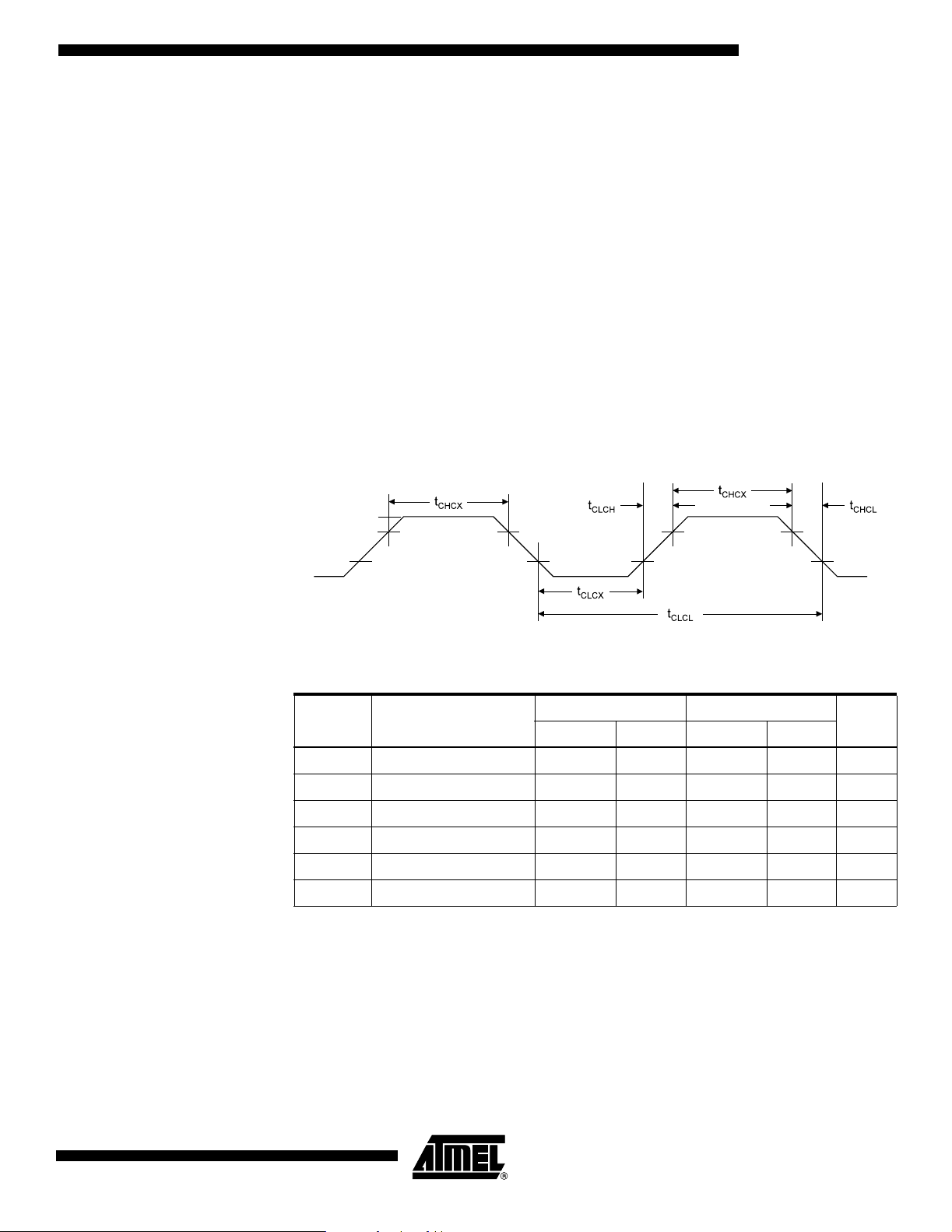
AT90S2313
Notes: 1. “Max” means the highest value where the pin is guaranteed to be read as low.
2. “Min” means the lowest value where the pin is guaranteed to be read as high.
3. Although each I/O port can sink more than the test conditions (20 mA at V
10 mA at V
be observed:
1] The sum of all I
2] The sum of all II
3] The sum of all I
If I
exceeds the test condition, VOLmay exceed the related specification. Pins are
OL
not guaranteed to sink current greater than the listed test condition.
4. Although each I/O port can source more than the test conditions (3 mA at V
1.5 mA at V
be observed:
1] The sum of all I
2] The sum of all I
3] The sum of all I
If I
exceeds the test condition, VOHmay exceed the related specification. Pins are
OH
not guaranteed to source current greater than the listed test condition.
5. Minimum V
= 3V) under steady state conditions (non-transient), the following must
CC
, for all ports, should not exceed 200 mA
OL
, for port D0 - D5 and XTAL2 should not exceed 100 mA.
OL
, for ports B0 - B7 and D6 should not exceed 100 mA.
OL
= 3V) under steady state conditions (non-transient), the following must
CC
, for all ports, should not exceed 200 mA
OH
, for port D0 - D5 and XTAL2 should not exceed 100 mA.
OH
, for ports B0 - B7 and D6 should not exceed 100 mA.
OH
for Power-down is 2V.
CC
CC
CC
=5V,
=5V,
External Clock Drive Waveforms
Figure 56. External Clock
VIH1
VIL1
External Clock Drive
Symbol Parameter
1/t
t
CLCL
t
CHCX
t
CLCX
t
CLCH
t
CHCL
CLCL
Oscillator Frequency 0 4 0 10.0 MHz
Clock Period 250.0 100.0 ns
High Time 100.0 40.0 ns
Low Time 100.0 40.0 ns
Rise Time 1.6 0.5 µs
Fall Time 1.6 0.5 µs
V
=2.7Vto6.0V VCC=4.0Vto6.0V
CC
UnitsMinMaxMinMax
0839I–AVR–06/02
73
Page 74

Typical Characteristics
The following charts show typical behavior. These figures are not tested during manufacturing. All current consumption measurements are performed with all I/O pins
configured as inputs and with internal pull-ups enabled. A sine wave generator with railto-rail output is used as clock source.
The power consumption in Power-down mode is independent of clock selection.
The current consumption is a function of several factors such as: operating voltage,
operating frequency, loading of I/O pins, switching rate of I/O pins, code executed and
ambient temperature. The dominating factors are operating voltage and frequency.
The current drawn from capacitive loaded pins may be estimated (for one pin) as
• VCC• fwhereCL= load capacitance, VCC= operating voltage and f = average
C
L
switching frequency of I/O pin.
The parts are characterized at frequencies higher than test limits. Parts are not guaranteed to function properly at frequencies higher than the ordering code indicates.
The difference between current consumption in Power-down mode with Watchdog
Timer enabled and Power-down mode with Watchdog Timer disabled represents the differential current drawn by the Watchdog Timer.
Figure 57. Active Supply Current vs. Frequency
ACTIVE SUPPLY CURRENT vs. FREQUENCY
25
20
15
(mA)
cc
I
10
5
0
0 1 2 3 4 5 6 7 8 9 10 11 12 13 14 15
T = 25˚C
A
Frequency (MHz)
V
= 2.7V
cc
V
V
V
V
V
V
V
V
= 6V
cc
= 5.5V
cc
= 5V
cc
= 4.5V
cc
= 4V
cc
= 3.6V
cc
= 3.3V
cc
= 3.0V
cc
74
AT90S2313
0839I–AVR–06/02
Page 75

AT90S2313
Figure 58. Active Supply Current vs. V
ACTIVE SUPPLY CURRENT vs. V
CC
FREQUENCY = 4 MHz
12
10
8
(mA)
cc
6
I
4
2
0
2 2.5 3 3.5 4 4.5 5 5.5 6
V
(V)
cc
Figure 59. Idle Supply Current vs. Frequency
cc
T = 25˚C
A
T = 85˚C
A
IDLE SUPPLY CURRENT vs. FREQUENCY
T = 25˚C
A
8
7
6
5
4
(mA)
cc
I
3
2
1
0
0 1 2 3 4 5 6 7 8 9 10 11 12 13 14 15
Frequency (MHz)
V
cc
= 2.7V
V
V
V
V
V
V
V
V
= 6V
cc
= 5.5V
cc
= 5V
cc
= 4.5V
cc
= 4V
cc
= 3.6V
cc
= 3.3V
cc
= 3.0V
cc
0839I–AVR–06/02
75
Page 76

Figure 60. Idle Supply Current vs. V
CC
IDLE SUPPLY CURRENT vs. V
FREQUENCY = 4 MHz
3.5
3
2.5
2
(mA)
cc
I
1.5
1
0.5
0
2 2.5 3 3.5 4 4.5 5 5.5 6
V
(V)
cc
Figure 61. Power-down Supply Current vs. V
POWER DOWN SUPPLY CURRENT vs. V
2
1.8
1.6
1.4
1.2
(µΑ)
cc
I
1
0.8
0.6
0.4
0.2
0
2 2.5 3 3.5 4 4.5 5 5.5 6
WATCHDOG TIMER DISABLED
V
(V)
cc
CC
cc
T = 25˚C
A
T = 85˚C
A
cc
T = 85˚C
A
T = 70˚C
A
T = 45˚C
A
T = 25˚C
A
76
AT90S2313
0839I–AVR–06/02
Page 77

AT90S2313
Figure 62. Power-down Supply Current vs. V
POWER DOWN SUPPLY CURRENT vs. V
160
140
120
100
(µΑ)
cc
80
I
60
40
20
0
2 2.5 3 3.5 4 4.5 5 5.5 6
WATCHDOG TIMER ENABLED
V
(V)
cc
Figure 63. Analog Comparator Current vs. V
CC
CC
cc
T = 25˚C
A
T = 85˚C
A
ANALOG COMPARATOR CURRENT vs. V
cc
0.9
0.8
0.7
T = 25˚C
A
0.6
T = 85˚C
0.5
(mA)
cc
I
0.4
0.3
0.2
0.1
0
2 2.5 3 3.5 4 4.5 5 5.5 6
V
(V)
cc
A
0839I–AVR–06/02
77
Page 78

Note: Analog Comparator offset voltage is measured as absolute offset.
Figure 64. Analog Comparator Offset Voltage vs. Common Mode Voltage
ANALOG COMPARATOR OFFSET VOLTAGE vs.
COMMON MODE VOLTAGE
18
16
14
12
10
8
Offset Voltage (mV)
6
4
2
0
0 0.5 1 1.5 2 2.5 3 3.5 4 4.5 5
Common Mode Voltage (V)
V = 5V
cc
T = 25˚C
A
T = 85˚C
A
Figure 65. Analog Comparator Offset Voltage vs. Common Mode Voltage
ANALOG COMPARATOR OFFSET VOLTAGE vs.
COMMON MODE VOLTAGE
10
8
V = 2.7V
cc
T = 25˚C
A
78
AT90S2313
6
4
Offset Voltage (mV)
2
0
0 0.5 1 1.5 2 2.5 3
Common Mode Voltage (V)
T = 85˚C
A
0839I–AVR–06/02
Page 79

Figure 66. Analog Comparator Input Leakage Current
AT90S2313
ANALOG COMPARATOR INPUT LEAKAGE CURRENT
V = 6V
CC
T = 25˚C
60
50
40
30
ACLK
I (nA)
20
10
0
-10
0 0.5 1.5122.53.53 4 4.5 5 6 6.5 75.5
V (V)
IN
Figure 67. Watchdog Oscillator Frequency vs. V
WATCHDOG OSCILLATOR FREQUENCY vs. V
A
CC
cc
1600
T = 25˚C
A
1400
1200
1000
800
RC
F (KHz)
600
400
200
0
2 2.5 3 3.5 4 4.5 5 5.5 6
V (V)
cc
T = 85˚C
A
0839I–AVR–06/02
79
Page 80

Note: Sink and source capabilities of I/O ports are measured on one pin at a time.
Figure 68. Pull-up Resistor Current vs. Input Voltage
PULL-UP RESISTOR CURRENT vs. INPUT VOLTAGE
120
100
80
OP
60
I (µA)
40
20
0
0 0.5 1 1.5 2 2.5 3 3.5 4 4.5 5
T = 25˚C
A
T = 85˚C
A
V = 5V
cc
V (V)
OP
Figure 69. Pull-up Resistor Current vs. Input Voltage
PULL-UP RESISTOR CURRENT vs. INPUT VOLTAGE
30
T = 25˚C
A
25
T = 85˚C
20
A
V = 2.7V
cc
80
AT90S2313
15
OP
I (µA)
10
5
0
0 0.5 1 1.5 2 2.5 3
V (V)
OP
0839I–AVR–06/02
Page 81

Figure 70. I/O Pin Sink Current vs. Output Voltage
AT90S2313
I/O PIN SINK CURRENT vs. OUTPUT VOLTAGE
70
V = 5V
cc
T = 25˚C
A
60
50
40
30
OL
I (mA)
20
10
0
0 0.5 1 1.5 2 2.5 3
V (V)
OL
Figure 71. I/O Pin Source Current vs. Output Voltage
I/O PIN SOURCE CURRENT vs. OUTPUT VOLTAGE
20
18
16
14
12
10
OH
8
I (mA)
6
4
2
0
0 0.5 1 1.5 2 2.5 3 3.5 4 4.5 5
T = 25˚C
A
T = 85˚C
A
V = 5V
cc
V (V)
OH
T = 85˚C
A
0839I–AVR–06/02
81
Page 82
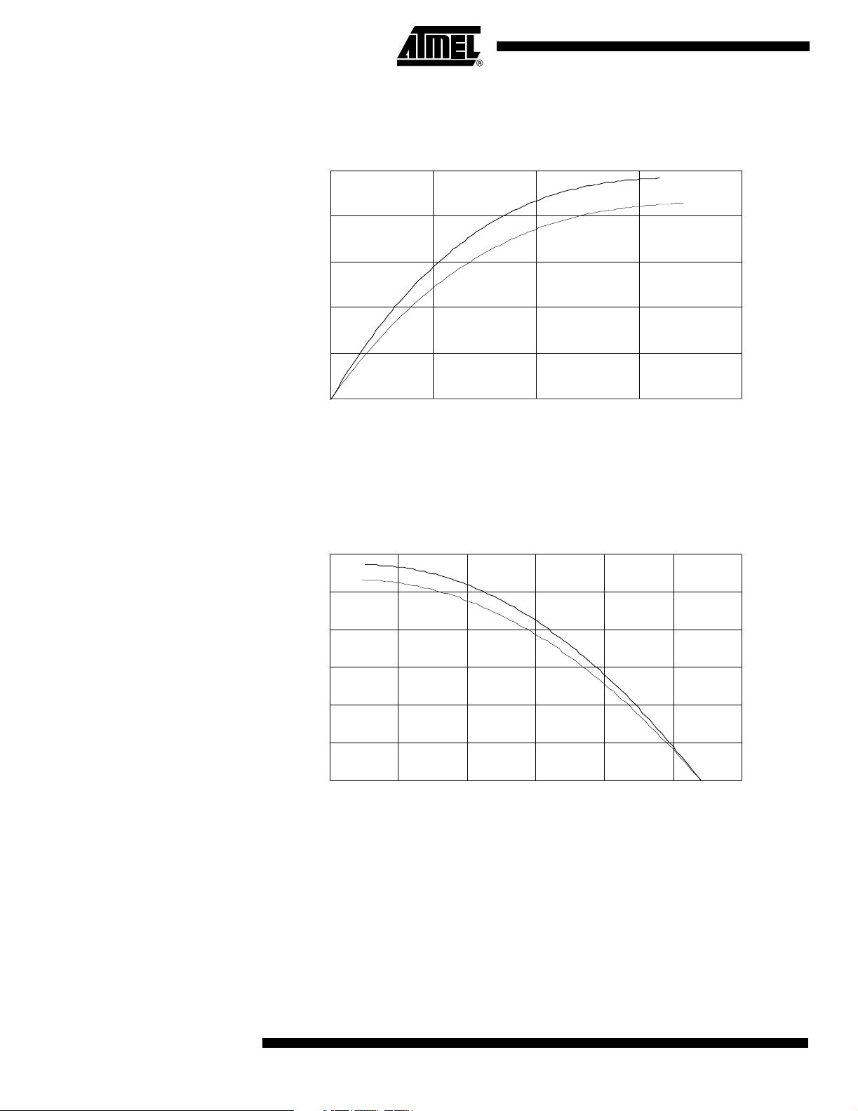
Figure 72. I/O Pin Sink Current vs. Output Voltage
I/O PIN SINK CURRENT vs. OUTPUT VOLTAGE
25
V = 2.7V
cc
T = 25˚C
A
20
T = 85˚C
A
15
10
OL
I (mA)
5
0
0 0.5 1 1.5 2
V (V)
OL
Figure 73. I/O Pin Source Current vs. Output Voltage
I/O PIN SOURCE CURRENT vs. OUTPUT VOLTAGE
6
T = 25˚C
A
V = 2.7V
cc
5
T = 85˚C
A
4
3
OH
I (mA)
2
1
0
0 0.5 1 1.5 2 2.5 3
V (V)
OH
82
AT90S2313
0839I–AVR–06/02
Page 83

AT90S2313
Figure 74. I/O Pin Input Threshold Voltage vs. V
I/O PIN INPUT THRESHOLD VOLTAGE vs. V
2.5
2
1.5
1
Threshold Voltage (V)
0.5
0
2.7 4.0 5.0
Figure 75. I/O Pin Input Hysteresis vs. V
T = 25˚C
A
V
cc
CC
CC
cc
I/O PIN INPUT HYSTERESIS vs. V
0.18
0.16
0.14
0.12
0.1
0.08
Input hysteresis (V)
0.06
0.04
0.02
0
2.7 4.0 5.0
T = 25˚C
A
V
cc
cc
0839I–AVR–06/02
83
Page 84
Register Summary
Address Name Bit 7 Bit 6 Bit 5 Bit 4 Bit 3 Bit 2 Bit 1 Bit 0 Page
$3F ($5F) SREG I T H S V N Z C page 16
$3E ($5E) Reserved
$3D ($5D) SPL SP7 SP6 SP5 SP4 SP3 SP2 SP1 SP0 page 17
$3C ($5C) Reserved
$3B ($5B) GIMSK INT1 INT0 – – – – – – page 22
$3A ($5A) GIFR INTF1 INTF0
$39 ($59) TIMSK TOIE1 OCIE1A
$38 ($58) TIFR TOV1 OCF1A – – ICF1 – TOV0 – page 24
$37 ($57) Reserved
$36 ($56) Reserved
$35 ($55) MCUCR – – SE SM ISC11 ISC10 ISC01 ISC00 page 25
$34 ($54) Reserved
$33 ($53) TCCR0 – – – – – CS02 CS01 CS00 page 29
$32 ($52) TCNT0 Timer/Counter0 (8 Bits) page 29
$31 ($51) Reserved
$30 ($50) Reserved
$2F ($4F) TCCR1A COM1A1 COM1A0 – – – – PWM11 PWM10 page 31
$2E ($4E) TCCR1B ICNC1 ICES1
$2D ($4D) TCNT1H Timer/Counter1 – Counter Register High Byte page 33
$2C ($4C) TCNT1L Timer/Counter1 – Counter Register Low Byte page 33
$2B ($4B) OCR1AH Timer/Counter1 – Compare Register High Byte page 34
$2A ($4A) OCR1AL Timer/Counter1 – Compare Register Low Byte page 34
$29 ($49) Reserved
$28 ($48) Reserved
$27 ($47) Reserved
$26 ($46) Reserved
$25 ($45) ICR1H Timer/Counter1 – Input Capture Register High Byte page 34
$24 ($44) ICR1L Timer/Counter1 – Input Capture Register Low Byte page 34
$23 ($43) Reserved
$22 ($42) Reserved
$21 ($41) WDTCR – – – WDTOE WDE WDP2 WDP1 WDP0 page 37
$20 ($40) Reserved
$1F ($3F) Reserved
$1E ($3E) EEAR – EEPROM Address Register page 39
$1D ($3D) EEDR EEPROM Data Register page 39
$1C ($3C) EECR – – – – – EEMWE EEWE EERE page 40
$1B ($3B) Reserved
$1A ($3A) Reserved
$19 ($39) Reserved
$18 ($38) PORTB PORTB7 PORTB6 PORTB5 PORTB4 PORTB3 PORTB2 PORTB1 PORTB0 page 50
$17 ($37) DDRB DDB7 DDB6 DDB5 DDB4 DDB3 DDB2 DDB1 DDB0 page 50
$16 ($36) PINB PINB7 PINB6 PINB5 PINB4 PINB3 PINB2 PINB1 PINB0 page 50
$15 ($35) Reserved
$14 ($34) Reserved
$13 ($33) Reserved
$12 ($32) PORTD – PORTD6 PORTD5 PORTD4 PORTD3 PORTD2 PORTD1 PORTD0 page 56
$11 ($31) DDRD – DDD6 DDD5 DDD4 DDD3 DDD2 DDD1 DDD0 page 56
$10 ($30) PIND
... Reserved
$0C ($2C) UDR UART I/O Data Register page 45
$0B ($2B) USR RXC T XC UDRE FE OR – – – page 45
$0A ($2A) U CR RXCIE TXCIE UDRIE RXEN TXEN CHR9 RXB8 TXB8 page 46
$09 ($29) UBRR UART Baud Rate Register page 48
$08 ($28) ACSR ACD – ACO ACI ACIE ACIC ACIS1 ACIS0 page 48
… Reserved
$00 ($20) Reserved
– PIND6 PIND5 PIND4 PIND3 PIND2 PIND1 PIND0 page 56
– – TICIE1 – TOIE0 – page 23
. – CTC1 CS12 CS11 CS10 page 32
Notes: 1. For compatibility with future devices, reserved bits should be written to zero if accessed. Reserved I/O memory addresses
should never be written.
2. Some of the Status Flags are cleared by writing a logical “1” to them. Note that the CBI and SBI instructions will operate on
all bits in the I/O Register, writing a “1” back into any flag read as set, thus clearing the flag. The CBI and SBI instructions
work with registers $00 to $1F only.
page 23
84
AT90S2313
0839I–AVR–06/02
Page 85

AT90S2313
Instruction Set Summary
Mnemonic Operands Description Operation Flags # Clocks
ARITHMETIC AND LOGIC INSTRUCTIONS
ADD Rd, Rr Add Two Registers Rd ← Rd + Rr Z,C,N,V,H 1
ADC Rd, Rr Add with Carry Two Registers Rd ← Rd + Rr + C Z,C,N,V,H 1
ADIW Rdl, K Add Immediate to Word Rdh:Rdl ← Rdh:Rdl + K Z,C,N,V,S 2
SUB Rd, Rr Subtract Two Registers Rd ← Rd − Rr Z,C,N,V,H 1
SUBI Rd, K Subtract Constant from Register Rd ← Rd − K Z,C,N,V,H 1
SBIW Rdl, K Subtract Immediate from Word Rdh:Rdl ← Rdh:Rdl − K Z,C,N,V,S 2
SBC Rd, Rr Subtract with Carry Two Registers Rd ← Rd − Rr − C Z,C,N,V,H 1
SBCI Rd, K Subtract with Carry Constant from Reg. Rd ← Rd − K − C Z,C,N,V,H 1
AND Rd, Rr Logical AND Registers Rd ← Rd • Rr Z,N,V 1
ANDI Rd, K Logical AND Register and Constant Rd ← Rd • K Z,N,V 1
OR Rd, Rr Logical OR Registers Rd ← Rd v Rr Z,N,V 1
ORI Rd, K Logical OR Register and Constant Rd ← Rd v K Z,N,V 1
EOR Rd, Rr Exclusive OR Registers Rd ← Rd ⊕ Rr Z,N,V 1
COM Rd One’s Complement Rd ← $FF − Rd Z,C,N,V 1
NEG Rd Two’s Complement Rd ← $00 − Rd Z,C,N,V,H 1
SBR Rd,K SetBit(s)inRegister Rd← Rd v K Z,N,V 1
CBR Rd, K Clear Bit(s) in Register Rd ← Rd • ($FF − K) Z,N,V 1
INC Rd Increment Rd ← Rd + 1 Z,N,V 1
DEC Rd Decrement Rd ← Rd − 1 Z,N,V 1
TST Rd Test for Zero or Minus Rd ← Rd • Rd Z,N,V 1
CLR Rd Clear Register Rd ← Rd ⊕ Rd Z,N,V 1
SER Rd Set Register Rd ← $FF None 1
BRANCH INSTRUCTIONS
RJMP k Relative Jump PC ← PC+k+1 None 2
IJMP Indirect Jump to (Z) PC ← Z None 2
RCALL k Relative Subroutine Call PC ← PC+k+1 None 3
ICALL Indirect Call to (Z) PC ← Z None 3
RET Subroutine Return PC ← STACK None 4
RETI Interrupt Return PC ← ST ACK I 4
CPSE Rd, Rr Compare, Skip if Equal if (Rd = Rr) PC ← PC + 2 or 3 None 1/2
CP Rd, Rr Compare Rd − Rr Z,N,V,C,H 1
CPC Rd, Rr Compare with Carry Rd − Rr − C Z,N,V,C,H 1
CPI Rd, K Compare Register with Immediate Rd − K Z,N,V,C,H 1
SBRC Rr, b Skip if Bit in Register Cleared if (Rr(b) = 0) PC ← PC + 2 or 3 None 1/2
SBRS Rr, b Skip if Bit in Register is Set if (Rr(b) = 1) PC ← PC + 2 or 3 None 1/2
SBIC P, b Skip if Bit in I/O Register Cleared if (P(b) = 0) PC ← PC + 2 or 3 None 1/2
SBIS P, b Skip if Bit in I/O Register is Set if (R(b) = 1) PC ← PC + 2 or 3 None 1/2
BRBS s, k Branch if Status Flag Set if (SREG(s) = 1) then PC ← PC + k + 1 None 1/2
BRBC s, k Branch if Status Flag Cleared if (SREG(s) = 0) then PC ← PC + k + 1 None 1/2
BREQ k Branch if Equal if (Z = 1) then PC ← PC + k + 1 None 1/2
BRNE k Branch if Not Equal if (Z = 0) then PC ← PC + k + 1 None 1/2
BRCS k Branch if Carry Set if (C = 1) then PC ← PC + k + 1 None 1/2
BRCC k Branch if Carry Cleared if (C = 0) then PC ← PC + k + 1 None 1/2
BRSH k Branch if Same or Higher if (C = 0) then PC ← PC + k + 1 None 1/2
BRLO k Branch if Lower if (C = 1) then PC ← PC + k + 1 None 1/2
BRMI k Branch if Minus if (N = 1) then PC ← PC + k + 1 None 1/2
BRPL k Branch if Plus if (N = 0) then PC ← PC + k + 1 None 1/2
BRGE k Branch if Greater or Equal, Signed if (N ⊕ V = 0) then PC ← PC + k + 1 None 1/2
BRLT k Branch if Less than Zero, Signed if (N ⊕ V = 1) then PC ← PC + k + 1 None 1/2
BRHS k Branch if Half-carry Flag Set if (H = 1) then PC ← PC + k + 1 None 1/2
BRHC k Branch if Half-carry Flag Cleared if (H = 0) then PC ← PC + k + 1 None 1/2
BRTS k Branch if T-Flag Set if (T = 1) then PC ← PC + k + 1 None 1/2
BRTC k Branch if T-Flag Cleared if (T = 0) then PC ← PC + k + 1 None 1/2
BRVS k Branch if Overflow Flag is Set if (V = 1) then PC ← PC + k + 1 None 1/2
BRVC k Branch if Overflow Flag is Cleared if (V = 0) then PC ← PC + k + 1 None 1/2
BRIE k Branch if Interrupt Enabled if (I = 1) then PC ← PC + k + 1 None 1/2
BRID k Branch if Interrupt Disabled if (I = 0) then PC ← PC + k + 1 None 1/2
0839I–AVR–06/02
85
Page 86

Instruction Set Summary (Continued)
Mnemonic Operands Description Operation Flags # Clocks
DATA TRANSFER INSTRUCTIONS
MOV Rd, Rr Move between Registers Rd ← Rr None 1
LDI Rd, K Load Immediate Rd ← K None 1
LD Rd, X Load Indirect Rd ← (X) None 2
LD Rd, X+ Load Indirect and Post-Inc. Rd ← (X ), X ← X + 1 None 2
LD Rd, -X Load Indirect and Pre-Dec. X ← X − 1, Rd ← (X) None 2
LD Rd, Y Load Indirect Rd ← (Y) None 2
LD Rd, Y+ Load Indirect and Post-Inc. Rd ← (Y ), Y ← Y + 1 None 2
LD Rd, -Y Load Indirect and Pre-Dec. Y ← Y − 1, Rd ← (Y) None 2
LDD Rd, Y+q Load Indirect with Displacement Rd ← (Y + q) None 2
LD Rd, Z Load Indirect Rd ← (Z) None 2
LD Rd, Z+ Load Indirect and Post-Inc. Rd ← (Z), Z ← Z+1 None 2
LD Rd, -Z Load Indirect and Pre-Dec. Z ← Z-1,Rd← (Z) None 2
LDD Rd, Z+q Load Indirect with Displacement Rd ← (Z + q) None 2
LDS Rd, k Load Direct from SRAM Rd ← (k) None 2
ST X, Rr Store Indirect (X) ← Rr None 2
ST X+, Rr Store Indirect and Post-Inc. (X) ← Rr, X ← X + 1 None 2
ST -X, Rr Store Indirect and Pre-Dec. X ← X-1,(X) ← Rr None 2
ST Y, Rr Store Indirect (Y) ← Rr None 2
ST Y+, Rr Store Indirect and Post-Inc. (Y) ← Rr, Y ← Y + 1 None 2
ST -Y, Rr Store Indirect and Pre-Dec. Y ← Y-1,(Y) ← Rr None 2
STD Y+q, Rr Store Indirect with Displacement (Y + q) ← Rr None 2
ST Z, Rr Store Indirect (Z) ← Rr None 2
ST Z+, Rr Store Indirect and Post-Inc. (Z) ← Rr, Z ← Z + 1 None 2
ST -Z, Rr Store Indirect and Pre-Dec. Z ← Z-1,(Z)← Rr None 2
STD Z+q, Rr Store Indirect with Displacement (Z + q) ← Rr None 2
STS k, Rr Store Direct to SRAM (k) ← Rr None 2
LPM Load Program Memory R0 ← (Z) None 3
IN Rd, P In Port Rd ← P None 1
OUT P, Rr Out Port P ← Rr None 1
PUSH Rr Push Register on Stack STACK ← Rr None 2
POP Rd Pop Register from Stack Rd ← STACK None 2
BIT AND BIT-TEST INSTRUCTIONS
SBI P, b Set Bit in I/O Register I/O(P,b) ← 1 None 2
CBI P, b Clear Bit in I/O Register I/O(P,b) ← 0 None 2
LSL Rd Logical Shift Left Rd(n+1) ← Rd(n), Rd(0) ← 0 Z,C,N,V 1
LSR Rd Logical Shift Right Rd(n) ← Rd(n+1), Rd(7) ← 0 Z,C,N,V 1
ROL Rd Rotate Left through Carry Rd(0) ← C, Rd(n+1) ← Rd(n), C ← Rd(7) Z,C,N,V 1
ROR Rd Rotate Right through Carry Rd(7) ← C, Rd(n) ← Rd(n+1), C ← Rd(0) Z ,C,N,V 1
ASR Rd Arithmetic Shift Right Rd(n) ← Rd(n+1), n = 0..6 Z,C,N,V 1
SWAP Rd Swap Nibble s Rd(3.. 0) ← Rd(7..4), Rd(7..4) ← Rd(3..0) None 1
BSET s Flag Set SREG(s) ← 1SREG(s)1
BCLR s Flag Clear SREG(s) ← 0SREG(s)1
BST Rr, b Bit Store from Register to T T ← Rr(b) T 1
BLD Rd, b Bit Load from T to Register Rd(b) ← T None 1
SEC Set Carry C ← 1C1
CLC Clear Carry C ← 0C1
SEN Set Negative Flag N ← 1N1
CLN Clear Negative Flag N ← 0N1
SEZ Set Zero Flag Z ← 1Z1
CLZ Clear Zero Flag Z ← 0Z1
SEI Global Interrupt Enable I ← 1I1
CLI Global Interrupt Disable I ← 0I1
SES Set Signed Test Flag S ← 1S1
CLS Clear Signed Test Flag S ← 0S1
SEV Set Two’s Complement Overflow V ← 1V1
CLV Clear Two’s Complement Overflow V ← 0V1
SET Set T in SREG T ← 1T1
CLT Clear T in SREG T ← 0T1
SEH SetHalf-carryFlaginSREG H← 1H1
CLH Clear Half-carry Flag in SREG H ← 0H1
NOP No Operation None 1
SLEEP Sleep (see specific descr. for Sleep function) None 1
WDR Watchdog Reset (see specific descr. for WDR/Timer) None 1
86
AT90S2313
0839I–AVR–06/02
Page 87
AT90S2313
Ordering Information
Speed (MHz) Power Supply Ordering Code Package Operation Range
4 2.7 - 6.0V AT90S2313-4PC
AT90S2313-4SC
AT90S2313-4PI
AT90S2313-4SI
10 4.0 - 6.0V AT90S2313-10PC
AT90S2313-10SC
AT90S2313-10PI
AT90S2313-10SI
20P3
20S
20P3
20S
20P3
20S
20P3
20S
Commercial
(0°Cto70°C)
Industrial
(-40°Cto85°C)
Commercial
(0°Cto70°C)
Industrial
(-40°Cto85°C)
Package Type
20P3 20-lead, 0.300" Wide, Plastic Dual Inline Package (PDIP)
20S 20-lead, 0.300" Wide, Plastic Gull Wing Small Outline (SOIC)
0839I–AVR–06/02
87
Page 88

Packaging Information
PIN
1
E1
A1
B
E
B1
C
L
SEATING PLANE
A
20P3
D
e
eC
eB
Notes: 1. This package conforms to JEDEC reference MS-001, Variation AD.
2. Dimensions D and E1 do not include mold Flash or Protrusion.
Mold Flash or Protrusion shall not exceed 0.25 mm (0.010").
2325 Orchard Parkway
R
San Jose, CA 95131
TITLE
20P3, 20-lead (0.300"/7.62 mm Wide) Plastic Dual
Inline Package (PDIP)
SYMBOL
A ––5.334
A1 0.381 ––
D 25.984 – 25.493 Note 2
E 7.620 – 8.255
E1 6.096 – 7.112 Note 2
B 0.356 – 0.559
B1 1.270 – 1.551
L 2.921 – 3.810
C 0.203 – 0.356
eB ––10.922
eC 0.000 – 1.524
e 2.540 TYP
COMMON DIMENSIONS
(Unit of Measure = mm)
MIN
NOM
MAX
NOTE
DRAWING NO.
20P3
09/28/01
REV.
B
88
AT90S2313
0839I–AVR–06/02
Page 89

20S
AT90S2313
20S, 20-lead, Plastic Gull Wing Small
Outline (SOIC), 0.300" body.
Dimensions in Millineters and (Inches)*
JEDEC STANDARD MS-013
0.51(0.020)
0.33(0.013)
PIN 1 ID
0º ~ 8º
PIN 1
1.27 (0.050) BSC
13.00 (0.5118)
12.60 (0.4961)
0.30(0.0118)
0.10 (0.0040)
0.32 (0.0125)
0.23 (0.0091)
7.60 (0.2992)
7.40 (0.2914)
2.65 (0.1043)
2.35 (0.0926)
10.65 (0.419)
10.00 (0.394)
0839I–AVR–06/02
1.27 (0.050)
0.40 (0.016)
*Controlling dimension: Inches
REV. A 04/11/2001
89
Page 90

AT90S2313
Table of Contents
Features................................................................................................. 1
Pin Configuration.................................................................................. 1
Description............................................................................................ 2
Pin Descriptions.................................................................................................... 3
Crystal Oscillator................................................................................................... 4
Architectural Overview......................................................................... 5
General Purpose Register File ............................................................................. 7
ALU – Arithmetic Logic Unit.................................................................................. 8
In-System Programmable Flash Program Memory .............................................. 8
EEPROM Data Memory........................................................................................ 8
SRAM Data Memory............................................................................................. 9
Program and Data Addressing Modes................................................................ 10
Memory Access and Instruction Execution Timing ............................................. 14
I/O Memory......................................................................................................... 15
Reset and Interrupt Handling.............................................................................. 18
Sleep Modes....................................................................................................... 27
Timer/Counters ................................................................................... 27
Timer/Counter Prescaler..................................................................................... 27
8-bit Timer/Counter0........................................................................................... 28
16-bit Timer/Counter1......................................................................................... 30
Watchdog Timer.................................................................................. 37
EEPROM Read/Write Access............................................................. 39
Prevent EEPROM Corruption............................................................................. 41
UART.................................................................................................... 42
Data Transmission.............................................................................................. 42
Data Reception................................................................................................... 43
UART Control ..................................................................................................... 45
Analog Comparator ............................................................................ 48
I/O Ports............................................................................................... 50
Port B.................................................................................................................. 50
Port D.................................................................................................................. 55
Memory Programming........................................................................ 60
Program and Data Memory Lock Bits................................................................. 60
Fuse Bits............................................................................................................. 60
Signature Bytes .................................................................................................. 60
Programming the Flash and EEPROM............................................................... 60
0839I–AVR–06/02
i
Page 91

Parallel Programming ......................................................................................... 61
Parallel Programming Characteristics ................................................................ 67
Serial Downloading............................................................................................. 68
Serial Programming Characteristics ................................................................... 71
Electrical Characteristics................................................................... 72
Absolute Maximum Ratings*............................................................................... 72
DC Characteristics.............................................................................................. 72
External Clock Drive Waveforms........................................................................ 73
External Clock Drive ........................................................................................... 73
Typical Characteristics ...................................................................... 74
Register Summary.............................................................................. 84
Instruction Set Summary ................................................................... 85
Ordering Information.......................................................................... 87
Packaging Information....................................................................... 88
20P3 ................................................................................................................... 88
20S ..................................................................................................................... 89
Table of Contents .................................................................................. i
ii
AT90S2313
0839I–AVR–06/02
Page 92

Atmel Headquarters Atmel Operations
Corporate Headquarters
2325 Orchard Parkway
San Jose, CA 95131
TEL 1(408) 441-0311
FAX 1(408) 487-2600
Europe
Atmel Sarl
Route des Arsenaux 41
Case Postale 80
CH-1705 Fribourg
Switzerland
TEL (41) 26-426-5555
FAX (41) 26-426-5500
Asia
Room 1219
Chinachem Golden Plaza
77 Mody Road Tsimhatsui
East Kowloon
Hong Kong
TEL (852) 2721-9778
FAX (852) 2722-1369
Japan
9F, Tonetsu Shinkawa Bldg.
1-24-8 Shinkawa
Chuo-ku, Tokyo 104-0033
Japan
TEL (81) 3-3523-3551
FAX (81) 3-3523-7581
Memory
2325 Orchard Parkway
San Jose, CA 95131
TEL 1(408) 441-0311
FAX 1(408) 436-4314
Microcontrollers
2325 Orchard Parkway
San Jose, CA 95131
TEL 1(408) 441-0311
FAX 1(408) 436-4314
La Chantrerie
BP 70602
44306 Nantes Cedex 3, France
TEL (33) 2-40-18-18-18
FAX (33) 2-40-18-19-60
ASIC/ASSP/Smart Cards
Zone Industrielle
13106 Rousset Cedex, France
TEL (33) 4-42-53-60-00
FAX (33) 4-42-53-60-01
1150 East Cheyenne Mtn. Blvd.
Colorado Springs, CO 80906
TEL 1(719) 576-3300
FAX 1(719) 540-1759
Scottish Enterprise Technology Park
Maxwell Building
East Kilbride G75 0QR, Scotland
TEL (44) 1355-803-000
FAX (44) 1355-242-743
RF/Automotive
Theresienstrasse 2
Postfach 3535
74025 Heilbronn, Germany
TEL (49) 71-31-67-0
FAX (49) 71-31-67-2340
1150 East Cheyenne Mtn. Blvd.
Colorado Springs, CO 80906
TEL 1(719) 576-3300
FAX 1(719) 540-1759
Biometrics/Imaging/Hi-Rel MPU/
High Speed Converters/RF Datacom
Avenue de Rochepleine
BP 123
38521 Saint-Egreve Cedex, France
TEL (33) 4-76-58-30-00
FAX (33) 4-76-58-34-80
e-mail
literature@atmel.com
Web Site
http://www.atmel.com
© Atmel Corporation 2002.
Atmel Corporation makes no warranty for the use of its products, other than those expressly contained in the Company’s standard warranty
whichisdetailedinAtmel’s Terms and Conditions located on the Company’s web site. The Company assumes no responsibility for any errors
which may appear in this document, reserves the right to change devices or specifications detailed herein at any time without notice, and does
not make any commitment to update the information contained herein. No licenses to patents or other intellectual property of Atmel are granted
by the Company in connection with the sale of Atmel products, expressly or by implication. Atmel’s products are not authorized for use as critical
components in life support devices or systems.
AT ME L®and AVR®are the registered trademarks of Atmel.
Other terms and product names may be the trademarks of others.
Printed on recycled paper.
0839I–AVR–06/02 0M
 Loading...