

Page 1

Features
• High-performance and Low-power AVR
– 118 Powerful Instructions – Most Single Cycle Execution
– 32x8GeneralPurposeWorkingRegisters
– Up to 8 MIPS Throughput at 8 MHz
• Data and Non-volatile Program Memory
– 4K Bytes of In-System Programmable Flash
Endurance 1,000 Write/Erase Cycles
– 128 Bytes of SRAM
– 256 Bytes of In-System Programmable EEPROM
Endurance: 100,000 Write/Erase Cycles
– Programming Lock for Flash Program and EEPROM Data Security
• Peripheral Features
– One 8-bit Timer/Counter with Separate Prescaler
– Expanded 16-bit Timer/Counter with Separate Prescaler,
Compare, Capture Modes and 8-, 9-, or 10-bit PWM
– On-chip Analog Comparator
– Programmable Watchdog Timer with Separate On-chip Oscillator
– Programmable UART
– 6-channel, 10-bit ADC
– Master/Slave SPI Serial Interface
• Special Microcontroller Features
– Brown-out Reset Circuit
– Enhanced Power-on Reset Circuit
– Low-power Idle and Power-down Modes
• Power Consumption at 4 MHz, 3V, 25°C
– Active: 3.4 mA
– Idle Mode: 1.4 mA
– Power-down Mode: <1 µA
• I/O and Packages
– 20 Programmable I/O Lines
– 28-lead PDIP and 32-lead TQFP
• Operating Voltage
– 2.7V - 6.0V for the AT90LS4433
– 4.0V - 6.0V for the AT90S4433
• Speed Grades
– 0 - 4 MHz for the AT90LS4433
– 0 - 8 MHz for the AT90S4433
®
8-bit RISC Architecture
8-bit
Microcontroller
with 4K Bytes of
In-System
Programmable
Flash
AT90S4433
AT90LS4433
Not Recommend for
New Designs. Use
ATmega8.
Rev. 1042G–AVR–09/02
1
Page 2
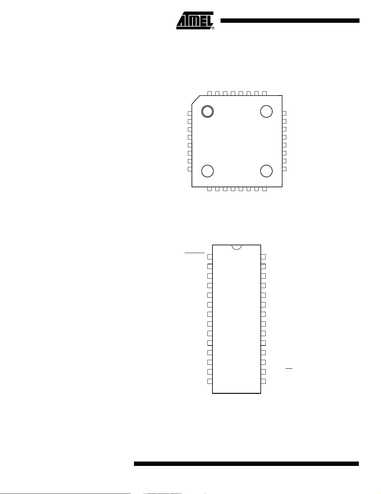
Pin Configurations TQFP Top View
PD2 (INT0)
PD1 (TXD)
PD0 (RXD)
RESET
PC5 (ADC5)
PC4 (ADC4)
PC3 (ADC3)
PC2 (ADC2)
(INT1) PD3
(T0) PD4
NC
VCC
GND
NC
XTAL1
XTAL2
(RXD) PD0
(TXD) PD1
(INT0) PD2
(INT1) PD3
(T0) PD4
(T1) PD5
(AIN0) PD6
(AIN1) PD7
(ICP) PB0
1
2
3
4
5
6
7
8
RESET
VCC
GND
XTAL1
XTAL2
32313029282726
9
10111213141516
(T1) PD5
(AIN0) PD6
(AIN1) PD7
1
2
3
4
5
6
7
8
9
10
11
12
13
14
PDIP
(SS) PB2
(ICP) PB0
(OC1) PB1
28
27
26
25
24
23
22
21
20
19
18
17
16
15
(MOSI) PB3
25
24
PC1 (ADC1)
23
PC0 (ADC0)
22
NC
21
AGND
20
AREF
19
NC
18
AVCC
17
PB5 (SCK)
(MISO) PB4
PC5 (ADC5)
PC4 (ADC4)
PC3 (ADC3)
PC2 (ADC2)
PC1 (ADC1)
PC0 (ADC0)
AGND
AREF
AVCC
PB5 (SCK)
PB4 (MISO)
PB3 (MOSI)
PB2 (SS)
PB1 (OC1)
2
AT90S/LS4433
1042G–AVR–09/02
Page 3

AT90S/LS4433
Description The AT90S4433 is a low-power CMOS 8-bit microcontroller based on the AVR RISC
architecture. By executing powerful instructions in a single clock cycle, the AT90S4433
achieves throughputs approaching 1 MIPS per MHz, allowing the system designer to
optimize power consumption versus processing speed.
The AVR core combines a rich instruction set with 32 general purpose working registers.
All the 32 registers are directly connected to the Arithmetic Logic Unit (ALU), allowing
two independent registers to be accessed in one single instruction, executed in one
clock cycle. The resulting architecture is more code efficient while achieving throughputs
up to ten times faster than conventional CISC microcontrollers.
The AT90S4433 provides the following features: 4K bytes of In-System Programmable
Flash, 256 bytes of EEPROM, 128 bytes of SRAM, 20 general purpose I/O lines, 32
general purpose working registers, two flexible Timer/Counters with compare modes,
internal and external interrupts, a programmable serial UART, 6-channel, 10-bit ADC,
programmable Watchdog Timer with internal Oscillator, an SPI serial port and two software-selectable Power-saving modes. The Idle mode stops the CPU while allowing the
SRAM, Timer/Counters, SPI port and interrupt system to continue functioning. The
Power-down mode saves the register contents but freezes the Oscillator, disabling all
other chip functions until the next interrupt or Hardware Reset.
The device is manufactured using Atmel’s high-density non-volatile memory technology.
The On-chip Flash Program memory can be re-programmed In-System through an SPI
serial interface or by a conventional non-volatile memory programmer. By combining a
RISC 8-bit CPU with In-System Programmable Flash on a monolithic chip, the Atmel
AT90S4433 is a powerful microcontroller that provides a highly flexible and cost-effective solution to many embedded control applications.
The AT90S4433 AVR is supported with a full suite of program and system development
tools including: C Compilers, macro assemblers, program debugger/simulators, In-Circuit Emulators and evaluation kits.
Table 1. Comparison Table
Device Flash EEPROM SRAM Voltage Range Frequency
AT90S4433 4K 256B 128B 4.0V - 6.0V 0 - 8 MHz
AT90LS4433 4K 256B 128B 2.7V - 6.0V 0 - 4 MHz
1042G–AVR–09/02
3
Page 4
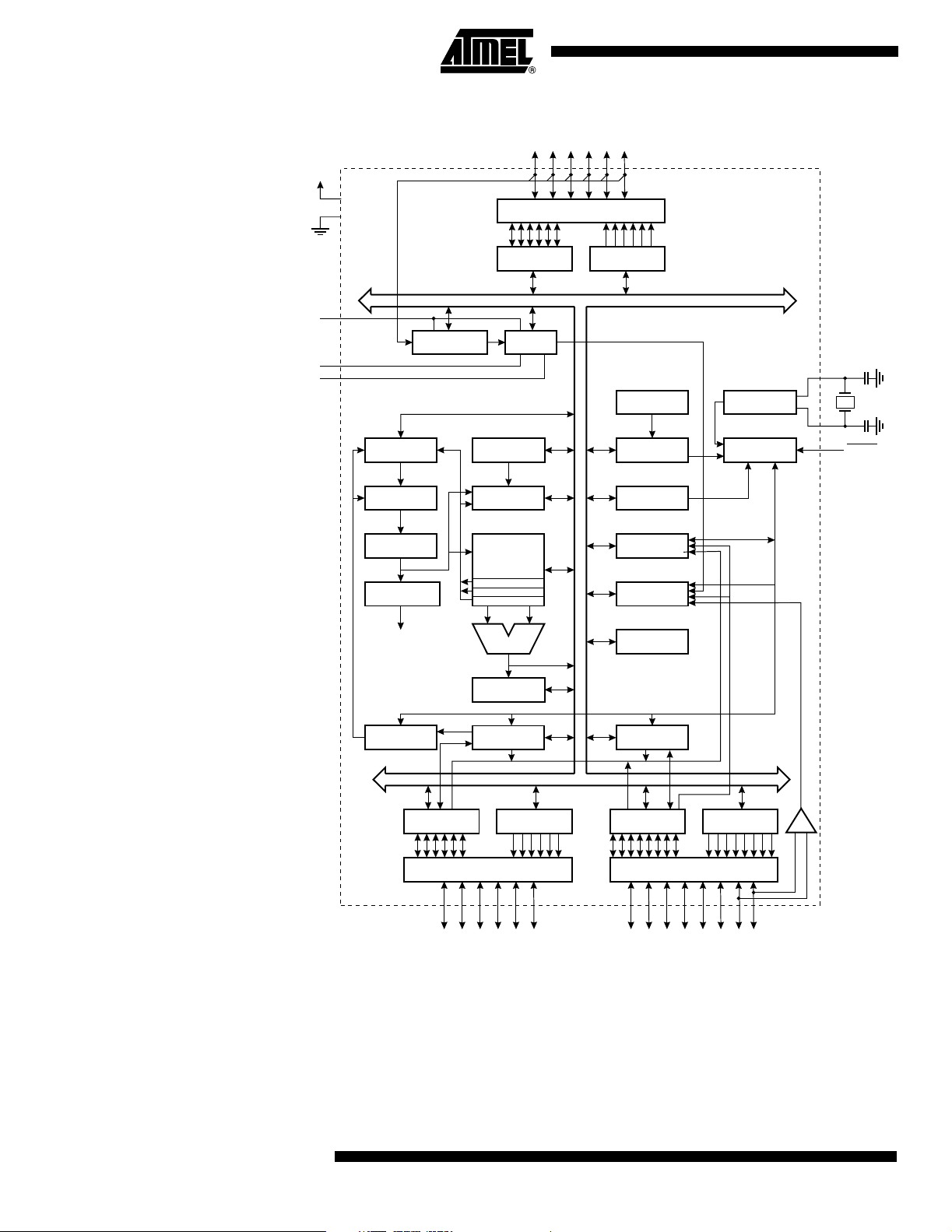
Block Diagram Figure 1. The AT90S4433 Block Diagram
PC0 - PC5
VCC
PORTC DRIVERS
GND
AVCC
AGND
AREF
PROGRAM
COUNTER
PROGRAM
FLASH
INSTRUCTION
REGISTER
INSTRUCTION
DECODER
CONTROL
LINES
DATA REGISTER
PORTC
ANALOG MUX ADC
STACK
POINTER
SRAM
GENERAL
PURPOSE
REGISTERS
X
Y
Z
ALU
STATUS
REGISTER
8-BIT DATA BUS
DATA DIR.
REG. PORTC
INTERNAL
OSCILLATOR
WATCHDOG
TIMER
MCU CONTROL
REGISTER
TIMER/
COUNTERS
INTERRUPT
EEPROM
UNIT
OSCILLATOR
TIMING AND
CONTROL
XTAL1
XTAL2
RESET
PROGRAMMING
LOGIC
DATA REGISTER
PORTB
PORTB DRIVERS
4
AT90S/LS4433
PB0 - PB5
SPI
DATA DIR.
REG. PORTB
UART
DATA REGISTER
PORTD
PORTD DRIVERS
PD0 - PD7
DATA DIR.
REG. PORTD
+
-
COMPARATOR
ANALOG
1042G–AVR–09/02
Page 5

AT90S/LS4433
Pin Descriptions
VCC Supply voltage.
GND Ground.
Port B (PB5..PB0) Port B is a 6-bit bi-directional I/O port with internal pull-up resistors. The Port B output
buffers can sink 20 mA. As inputs, Port B pins that are externally pulled low will source
current if the pull-up resistors are activated.
Port B also serves the functions of various special features of the AT90S4433 as listed
on page 73.
The Port B pins are tri-stated when a reset condition becomes active, even if the clock is
not running.
Port C (PC5..PC0) Port C is a 6-bit bi-directional I/O port with internal pull-up resistors. The Port C output
buffers can sink 20 mA. As inputs, Port C pins that are externally pulled low will source
current if the pull-up resistors are activated. Port C also serves as the analog inputs to
the A/D Converter.
The Port C pins are tri-stated when a reset condition becomes active, even if the clock is
not running.
Port D (PD7..PD0) Port D is an 8-bit bi-directional I/O port with internal pull-up resistors. The Port D output
buffers can sink 20 mA. As inputs, Port D pins that are externally pulled low will source
current if the pull-up resistors are activated.
Port D also serves the functions of various special features of the AT90S4433 as listed
on page 81.
The Port D pins are tri-stated when a reset condition becomes active, even if the clock is
not running.
RESET
XTAL1 Input to the inverting oscillator amplifier and input to the internal clock operating circuit
XTAL2 Output from the inverting oscillator amplifier
AVCC AVCC is the supply voltage for Port A and the A/D Converter. If the ADC is not used,
AREF AREF is the analog reference input for the A/D Converter. For ADC operations, a volt-
AGND If the board has a separate analog ground plane, this pin should be connected to this
Reset input. An External Reset is generated by a low level on the RESET pin. Reset
pulses longer than 50 ns will generate a reset, even if the clock is not running. Shorter
pulses are not guaranteed to generate a reset.
this pin must be connected to V
V
via a low-pass filter. See page 64 for details on operation of the ADC.
CC
age in the range 2.0V to AVCC must be applied to this pin.
ground plane. Otherwise, connect to GND.
. If the ADC is used, this pin should be connected to
CC
1042G–AVR–09/02
5
Page 6
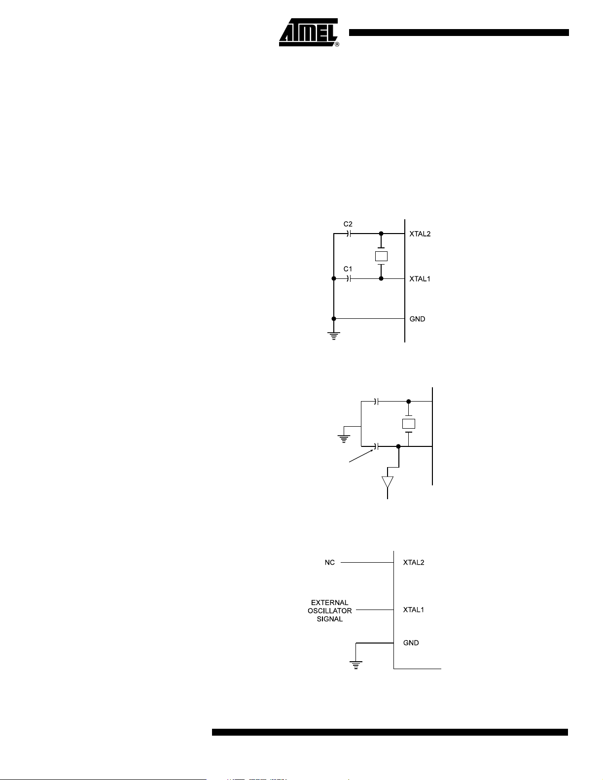
Clock Options
Crystal Oscillator XTAL1 and XTAL2 are input and output, respectively, of an inverting amplifier, which
can be configured for use as an On-chip Oscillator, as shown in Figure 2 and Figure 3.
Either a quartz crystal or a ceramic resonator may be used.
External Clock If the Oscillator is to be used as a clock for an external device, the clock signal from
XTAL2 may be routed to one HC buffer while reducing the load capacitor by 5 pF, as
shown in Figure 3. To drive the device from an external clock source, XTAL2 should be
left unconnected while XTAL1 is driven as shown in Figure 4.
Figure 2. Oscillator Connections
Figure 3. Using MCU Oscillator as a Clock for an External Device
XTAL1
XTAL2
REDUCE BY 5
F
P
HC
MAX 1 HC BUFFER
Figure 4. External Clock Drive Configuration
6
AT90S/LS4433
1042G–AVR–09/02
Page 7
AT90S/LS4433
Architectural Overview
The fast-access Register File concept contains 32 x 8-bit general purpose working registers with a single clock cycle access time. This means that during one single clock
cycle, one Arithmetic Logic Unit (ALU) operation is executed. Two operands are output
from the Register File, the operation is executed, and the result is stored back in the
Register File – in one clock cycle.
Six of the 32 registers can be used as three 16-bit indirect address register pointers for
Data Space addressing, enabling efficient address calculations. One of the three
address pointers is also used as the address pointer for the constant table look-up function. These added function registers are the 16-bit X-, Y-, and Z-register.
The ALU supports arithmetic and logic functions between registers or between a constant and a register. Single register operations are also executed in the ALU. Figure 5
shows the AT90S4433 AVR RISC microcontroller architecture.
In addition to the register operation, the conventional Memory Addressing modes can be
used on the Register File as well. This is enabled by the fact that the Register File is
assigned the 32 lowermost Data Space addresses ($00 - $1F), allowing them to be
accessed as though they were ordinary memory locations.
Figure 5. The AT90S4433 AVR RISC Architecture
Data Bus 8-bit
2K X 16
Program
Memory
Program
Counter
Status
and Control
Interrupt
Unit
Instruction
Register
Instruction
Decoder
Control Lines
Direct Addressing
Indirect Addressing
32 x 8
General
Purpose
Registrers
ALU
128 x 8
Data
SRAM
256 x 8
EEPROM
20
I/O Lines
SPI
Unit
Serial
UART
8-bit
Timer/Counter
16-bit
Timer/Counter
with PWM
Watchdog
Timer
Analog to Digital
Converter
Analog
Comparator
1042G–AVR–09/02
7
Page 8

The I/O memory space contains 64 addresses for CPU peripheral functions such as
Control Registers, Timer/Counters, A/D Converters and other I/O functions. The I/O
memory can be accessed directly, or as the Data Space locations following those of the
Register File, $20 - $5F.
The AVR uses a Harvard architecture concept – with separate memories and buses for
program and data. The Program memory is executed with a two-stage pipeline. While
one instruction is being executed, the next instruction is pre-fetched from the Program
memory. This concept enables instructions to be executed in every clock cycle.
The Program memory is In-System Programmable Flash memory.
With the relative jump and call instructions, the whole 2K word address space is directly
accessed. Most AVR instructions have a single 16-bit word format. Every program
memory address contains a 16- or 32-bit instruction.
During interrupts and subroutine calls, the return address Program Counter (PC) is
stored on the Stack. The Stack is effectively allocated in the general data SRAM and,
consequently, the Stack size is only limited by the total SRAM size and the usage of the
SRAM. All user programs must initialize the SP in the reset routine (before subroutines
or interrupts are executed). The 8-bit Stack Pointer (SP) is read/write accessible in the
I/O space.
The 128 bytes of data SRAM can be easily accessed through the five different addressing modes supported in the AVR architecture.
The memory spaces in the AVR architecture are all linear and regular memory maps.
8
AT90S/LS4433
1042G–AVR–09/02
Page 9
Figure 6. AT90S4433 Memory Maps
AT90S/LS4433
Data MemoryProgram Memory
Program Flash
(2K x 16)
$000
32 Gen. Purpose
Working Registers
64 I/O Registers
Internal SRAM
(128 x 8)
$0000
$001F
$0020
$005F
$0060
$00DF
$7FF
A flexible interrupt module has its control registers in the I/O space with an additional
Global Interrupt Enable bit in the Status Register. All the different interrupts have a separate Interrupt Vector in the Interrupt Vector table at the beginning of the Program
memory. The different interrupts have priority in accordance with their Interrupt Vector
position. The lower the Interrupt Vector address, the higher the priority.
1042G–AVR–09/02
9
Page 10
General Purpose Register File
Figure 7 shows the structure of the 32 general purpose working registers in the CPU.
Figure 7. AVR CPU General Purpose Working Registers
7 0 Addr.
R0 $00
R1 $01
R2 $02
…
R13 $0D
General R14 $0E
Purpose R15 $0F
Working R16 $10
Registers R17 $11
…
R26 $1A X-register Low Byte
R27 $1B X-register High Byte
R28 $1C Y-register Low Byte
R29 $1D Y-register High Byte
R30 $1E Z-register Low Byte
R31 $1F Z-register High Byte
All the register operating instructions in the instruction set have direct and single cycle
access to all registers. The only exceptions are the five constant arithmetic and logic
instructions SBCI, SUBI, CPI, ANDI, and ORI between a constant and a register, and
the LDI instruction for load immediate constant data. These instructions apply to the
second half of the registers in the Register File (R16..R31). The general SBC, SUB, CP,
AND, and OR, and all other operations between two registers or on a single register
apply to the entire Register File.
X-register, Y-register and Zregister
As shown in Figure 7, each register is also assigned a data memory address, mapping
them directly into the first 32 locations of the user Data Space. Although not being physically implemented as SRAM locations, this memory organization provides great
flexibility in access of the registers, as the X-, Y- ,and Z-registers can be set to index any
register in the file.
The registers R26..R31 have some added functions to their general purpose usage.
These registers are address pointers for indirect addressing of the Data Space. The
three indirect address registers X, Y, and Z are defined as:
Figure 8. X-, Y-, and Z-registers
15 0
X - register 7070
R27 ($1B) R26 ($1A)
15 0
Y - register
Z-register
7070
R29 ($1D) R28 ($1 C)
15 0
7070
R31 ($1F) R30 ($1E)
10
AT90S/LS4433
1042G–AVR–09/02
Page 11
AT90S/LS4433
In the different addressing modes, these address registers have functions as fixed displacement, automatic increment and decrement (see the descriptions for the different
instructions).
ALU – Arithmetic Logic Unit
In-System Programmable Flash Program Memory
The high-performance AVR ALU operates in direct connection with all the 32 general
purpose working registers. Within a single clock cycle, ALU operations between registers in the Register File are executed. The ALU operations are divided into three main
categories: arithmetic, logical, and bit functions.
The AT90S4433 contains 4K bytes of On-chip, In-System Programmable Flash memory
for program storage. Since all instructions are 16- or 32-bit words, the Flash is organized as 2K x 16. The Flash memory has an endurance of at least 1,000 write/erase
cycles. The AT90S4433 Program Counter (PC) is 11 bits wide, thus addressing the
2,048 program memory addresses. See page 93 for a detailed description of Flash data
downloading. See page 12 for the different program memory addressing modes.
Figure 9. SRAM Organization
Register File Data Address Spa ce
R0 $0000
R1 $0001
R2 $0002
º º
R29 $001D
R30 $001E
R31 $001F
I/O Registers
$00 $0020
$01 $0021
$02 $0022
……
$3D $005D
$3E $005E
$3F $005F
SRAM Data Memory Figure 9 shows how the AT90S4433 SRAM memory is organized.
The lower 224 data memory locations address the Register File, the I/O memory and
the internal data SRAM. The first 96 locations address the Register File and I/O memory, and the next 128 locations address the internal data SRAM.
The five different addressing modes for the data memory cover: Direct, Indirect with Displacement, Indirect, Indirect with Pre-decrement, and Indirect with Post-increment. In
the Register File, registers R26 to R31 feature the indirect addressing pointer registers.
1042G–AVR–09/02
Internal SRAM
$0060
$0061
º
$00DE
$00DF
11
Page 12
The direct addressing reaches the entire data space. The Indirect with Displacement
mode features 63 address locations reached from the base address given by the Y- or
Z-register.
When using register indirect addressing modes with automatic pre-decrement and postincrement, the address registers X, Y, and Z are decremented and incremented.
The 32 general purpose working registers, 64 I/O Registers and the 128 bytes of internal data SRAM in the AT90S4433 are all accessible through all these addressing
modes.
See the next section for a detailed description of the different addressing modes.
Program and Data Addressing Modes
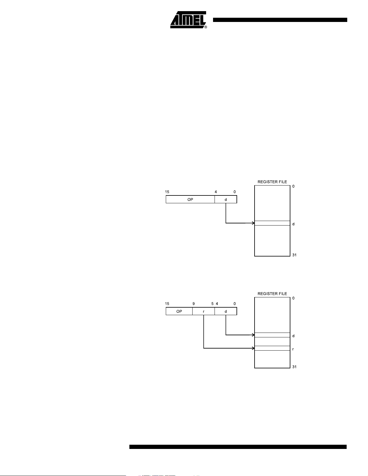
Register Direct, Single Register Rd
Register Direct, Two Registers Rd and Rr
The AT90S4433 AVR RISC microcontroller supports powerful and efficient addressing
modes for access to the Flash Program memory, SRAM, Register File, and I/O data
memory. This section describes the different addressing modes supported by the AVR
architecture. In the figures, OP means the operation code part of the instruction word.
To simplify, not all figures show the exact location of the addressing bits.
Figure 10. Direct Single Register Addressing
The operand is contained in register d (Rd).
Figure 11. Direct Register Addressing, Two Registers
12
Operands are contained in registers r (Rr) and d (Rd). The result is stored in register d
(Rd).
AT90S/LS4433
1042G–AVR–09/02
Page 13
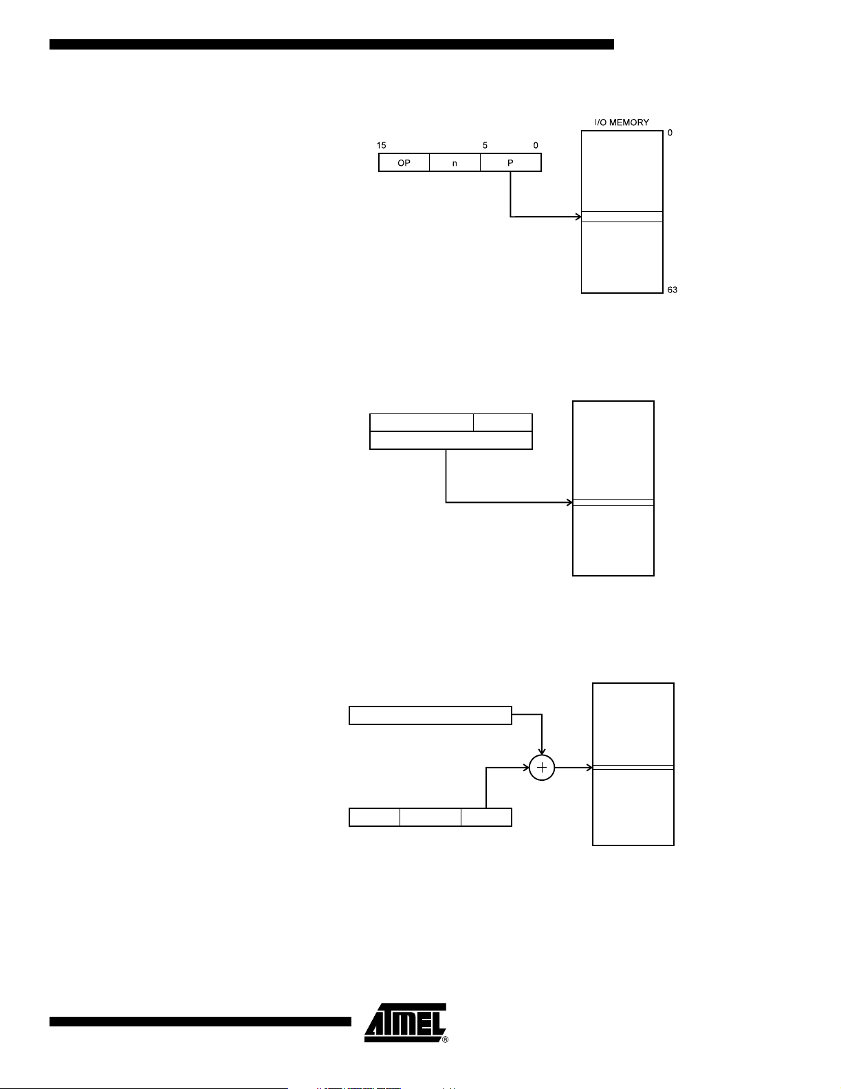
I/O Direct Figure 12. I/O Direct Addressing
Operand address is contained in six bits of the instruction word. n is the destination or
source register address.
Data Direct Figure 13. Direct Data Addressing
31
OP Rr/Rd
15 0
20 19
16 LSBs
AT90S/LS4433
Data Space
16
$0000
Data Indirect with Displacement
$00DF
A 16-bit data address is contained in the 16 LSBs of a two-word instruction. Rd/Rr specify the destination or source register.
Figure 14. Data Indirect with Displacement
15
Y OR Z - REGISTER
15
OP an
Data Space
0
05610
$0000
$00DF
Operand address is the result of the Y- or Z-register contents added to the address contained in six bits of the instruction word.
1042G–AVR–09/02
13
Page 14
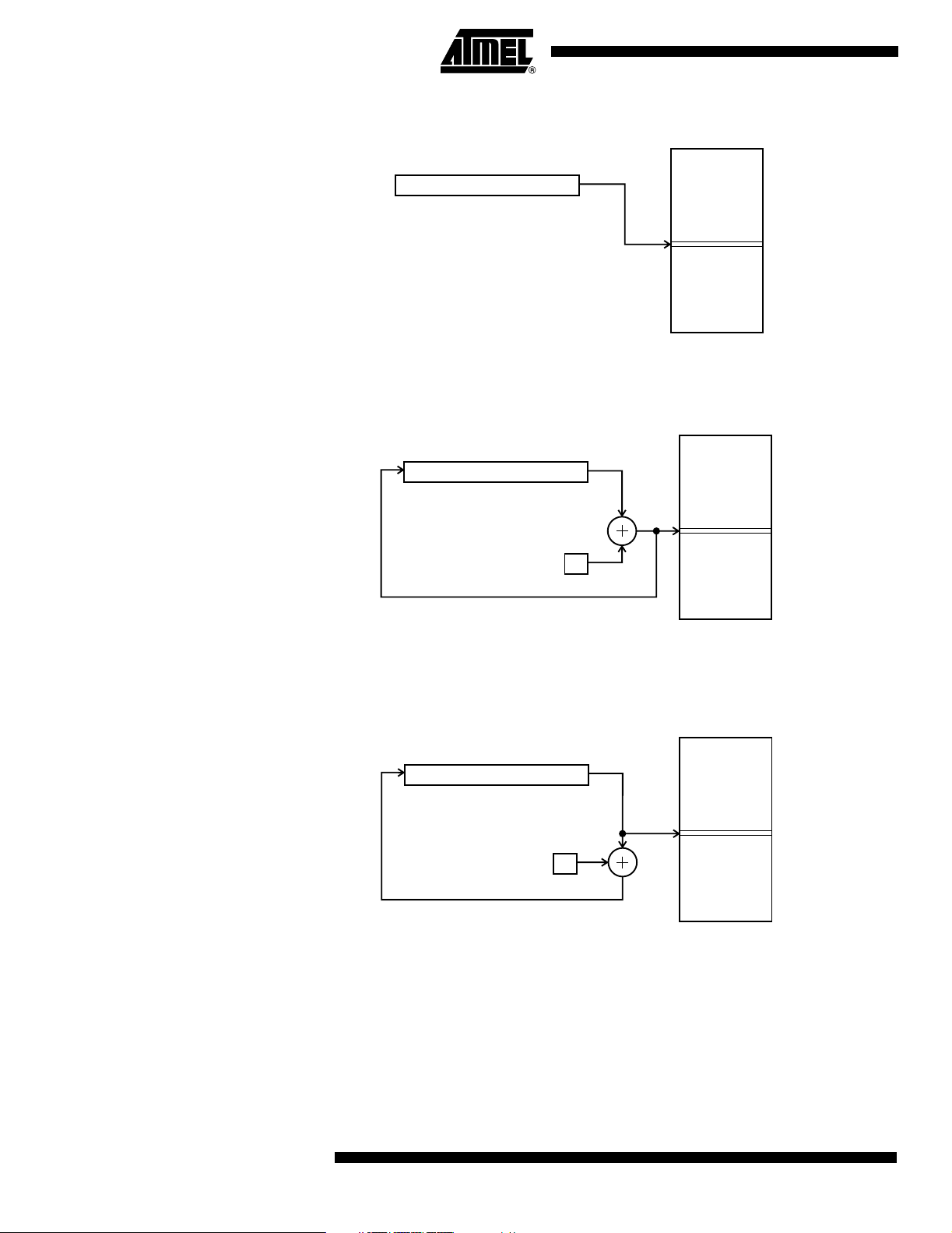
Data Indirect Figure 15. Data Indirect Addressing
X, Y, OR Z - REGISTER
Operand address is the contents of the X-, Y-, or the Z-register.
Data Space
015
$0000
$00DF
Data Indirect with Predecrement
Data Indirect with Postincrement
Figure 16. Data Indirect Addressing with Pre-decrement
Data Space
015
X, Y, OR Z - REGISTER
-1
$0000
$00DF
The X-, Y-, or the Z-register is decremented before the operation. Operand address is
the decremented contents of the X-, Y-, or the Z-register.
Figure 17. Data Indirect Addressing with Post-increment
Data Space
015
X, Y, OR Z - REGISTER
$0000
14
1
$00DF
The X-, Y-, or the Z-register is incremented after the operation. Operand address is the
content of the X-, Y-, or the Z-register prior to incrementing.
AT90S/LS4433
1042G–AVR–09/02
Page 15
AT90S/LS4433
Constant Addressing Using the LPM Instruction
Indirect Program Addressing, IJMP and ICALL
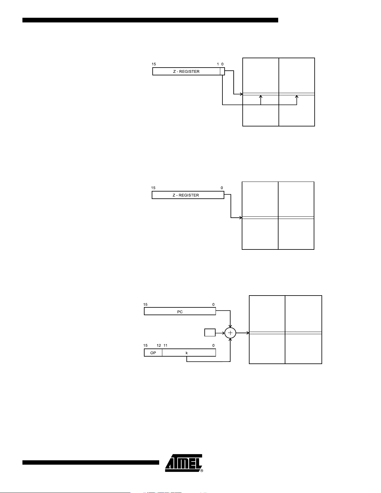
Figure 18. Code Memory Constant Addressing
PROGRAM MEMORY
$000
$7FF
Constant byte address is specified by the Z-register contents. The 15 MSBs select word
address (0 - 2K), the LSB selects Low Byte if cleared (LSB = 0) or High Byte if set
(LSB = 1).
Figure 19. Indirect Program Memory Addressing
PROGRAM MEMORY
$000
Relative Program Addressing, RJMP and RCALL
$7FF
Program execution continues at address contained by the Z-register (i.e., the PC is
loaded with the contents of the Z-register).
Figure 20. Relative Program Memory Addressing
PROGRAM MEMORY
+1
$000
$7FF
Program execution continues at address PC + k + 1. The relative address k is from
-2048 to 2047.
1042G–AVR–09/02
15
Page 16
EEPROM Data Memory The AT90S4433 contains 256 bytes of data EEPROM memory. It is organized as a sep-
arate data space, in which single bytes can be read and written. The EEPROM has an
endurance of at least 100,000 write/erase cycles per location. The access between the
EEPROM and the CPU is described on page 53, specifying the EEPROM Address Registers, the EEPROM Data Register and the EEPROM Control Register.
For the SPI Data downloading, see page 93 for a detailed description. The EEPROM
Data memory is In-System Programmable through the SPI port. Please refer to the
“EEPROM Read/Write Access” section on page 45 for a thorough description of
EEPROM access.
Memory Access Times and Instruction Execution Timing
This section describes the general access timing concepts for instruction execution and
internal memory access.
TheAVRCPUisdrivenbytheSystemClockØ, directly generated from the external
clock crystal for the chip. No internal clock division is used.
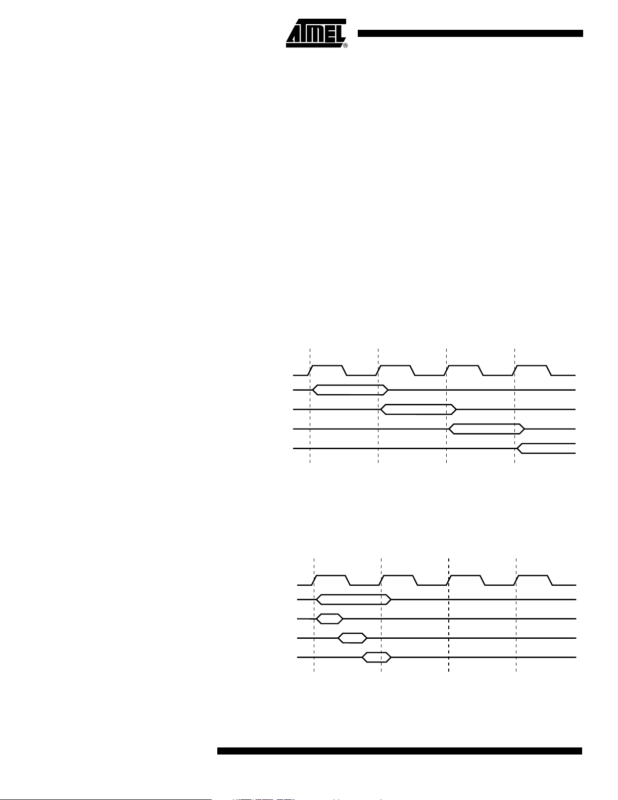
Figure 21 shows the parallel instruction fetches and instruction executions enabled by
the Harvard architecture and the fast-access Register File concept. This is the basic
pipelining concept to obtain up to 1 MIPS per MHz with the corresponding unique results
for functions per cost, functions per clocks and functions per power unit.
Figure 21. The Parallel Instruction Fetches and Instruction Executions
T1 T2 T3 T4
System Clock Ø
1st Instruction Fetch
1st Instruction Execute
2nd Instruction Fetch
2nd Instruction Execute
3rd Instruction Fetch
3rd Instruction Execute
4th Instruction Fetch
Figure 22 shows the internal timing concept for the Register File. In a single clock cycle
an ALU operation using two register operands is executed and the result is stored back
to the destination register.
16
Figure 22. Single Cycle ALU Operation
T1 T2 T3 T4
System Clock Ø
Total Execution Time
Register Operands Fetch
ALU Operation Execute
Result Write Back
The internal data SRAM access is performed in two System Clock cycles as described
in Figure 23.
AT90S/LS4433
1042G–AVR–09/02
Page 17
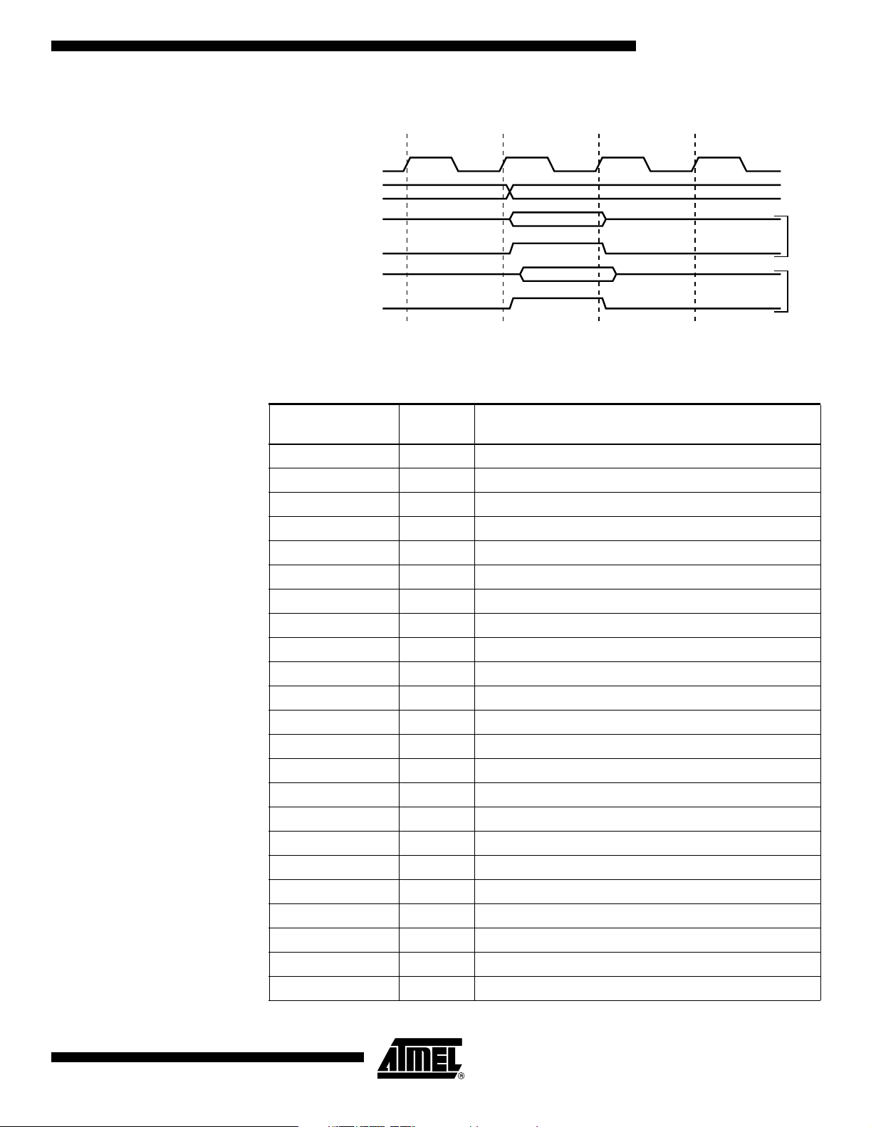
Figure 23. On-chip Data SRAM Access Cycles
T1 T2 T3 T4
System Clock Ø
AT90S/LS4433
Address
Data
WR
Data
RD
Prev. Address
Address
I/O Memory The I/O space definition of the AT90S4433 is shown in Table 2.
Table 2. AT90S4433 I/O Space
I/O Address
(SRAM Address) Name Function
$3F ($5F) SREG Status Register
$3D ($5D) SP Stack Pointer
$3B ($5B) GIMSK General Interrupt MaSK Register
$3A ($5A) GIFR General Interrupt Flag Register
$39 ($59) TIMSK Timer/Counter Interrupt MaSK Register
$38 ($58) TIFR Timer/Counter Interrupt Flag Register
$35 ($55) MCUCR MCU general Control Register
$34 ($54) MCUSR MCU general Status Register
(1)
Write
Read
1042G–AVR–09/02
$33 ($53) TCCR0 Timer/Counter0 Control Register
$32 ($52) TCNT0 Timer/Counter0 (8-bit)
$2F ($4F) TCCR1A Timer/Counter1 Control Register A
$2E ($4E) TCCR1B Timer/Counter1 Control Register B
$2D ($4D) TCNT1H Timer/Counter1 High Byte
$2C ($4C) TCNT1L Timer/Counter1 Low Byte
$2B ($4B) OCR1H Timer/Counter1 Output Compare Register High Byte
$2A ($4A) OCR1L Timer/Counter1 Output Compare Register Low Byte
$27 ($47) ICR1H Timer/Counter1 Input Capture Register High Byte
$26 ($46) ICR1L Timer/Counter 1 Input Capture Register Low Byte
$21 ($41) WDTCR Watchdog Timer Control Register
$1E ($3E) EEAR EEPROM Address Register
$1D ($3D) EEDR EEPROM Data Register
$1C ($3C) EECR EEPROM Control Register
$18 ($38) PORTB Data Register, Port B
17
Page 18

Table 2. AT90S4433 I/O Space
I/O Address
(SRAM Address) Name Function
$17 ($37) DDRB Data Direction Register, Port B
$16 ($36) PINB Input Pins, Port B
$15 ($35) PORTC Data Register, Port C
$14 ($34) DDRC Data Direction Register, Port C
$13 ($33) PINC Input Pins, Port C
$12 ($32) PORTD Data Register, Port D
$11 ($31) DDRD Data Direction Register, Port D
$10 ($30) PIND Input Pins, Port D
$0F ($2F) SPDR SPI I/O Data Register
$0E ($2E) SPSR SPI Status Register
$0D ($2D) SPCR SPI Control Register
$0C ($2C) UDR UART I/O Data Register
$0B ($2B) UCSRA UART Control and Status Register A
$0A ($2A) UCSRB UART Control and Status Register B
$09 ($29) UBRR UART Baud Rate Register
(1)
(Continued)
$08 ($28) ACSR Analog Comparator Control and Status Register
$07 ($27) ADMUX ADC Multiplexer Select Register
$06 ($26) ADCSR ADC Control and Status Register
$05 ($25) ADCH ADC Data Register High
$04 ($24) ADCL ADC Data Register Low
$03 ($23) UBRRHI UART Baud Rate Register High
Note: 1. Reserved and unused locations are not shown in the table.
All AT90S4433 I/Os and peripherals are placed in the I/O space. The I/O locations are
accessed by the IN and OUT instructions transferring data between the 32 general purpose working registers and the I/O space. I/O Registers within the address range $00 $1F are directly bit-accessible using the SBI and CBI instructions. In these registers, the
value of single bits can be checked by using the SBIS and SBIC instructions. Refer to
the instruction set section for more details. When using the I/O specific commands IN
and OUT, the I/O addresses $00 - $3F must be used. When addressing I/O Registers as
SRAM, $20 must be added to this address. All I/O Register addresses throughout this
document are shown with the SRAM address in parentheses.
For compatibility with future devices, reserved bits should be written to zero when
accessed. Reserved I/O memory addresses should never be written.
Some of the Status Flags are cleared by writing a logical “1” to them. Note that the CBI
and SBI instructions will operate on all bits in the I/O Register, writing a one back into
any flag read as set, thus clearing the flag. The CBI and SBI instructions work with registers $00 to $1F only.
18
The I/O and Peripherals Control Registers are explained in the following sections.
AT90S/LS4433
1042G–AVR–09/02
Page 19

AT90S/LS4433
Status Register – SREG The AVR Status Register (SREG) at I/O space location $3F ($5F) is defined as:
Bit 76543210
$3F ($5F) I THSVNZCSREG
Read/Write R/W R/W R/W R/W R/W R/W R/W R/W
InitialValue00000000
• Bit 7 – I: Global Interrupt Enable
The Global Interrupt Enable bit must be set (one) for the interrupts to be enabled. The
individual interrupt enable control is then performed in separate control registers. If the
Global Interrupt Enable Register is cleared (zero), none of the interrupts are enabled
independent of the individual interrupt enable settings. The I-bit is cleared by hardware
after an interrupt has occurred and is set by the RETI instruction to enable subsequent
interrupts.
• Bit 6 – T: Bit Copy Storage
The Bit Copy Instructions BLD (Bit LoaD) and BST (Bit STore) use the T-bit as source
and destination for the operated bit. A bit from a register in the Register File can be copied into T by the BST instruction, and a bit in T can be copied into a bit in a register in the
Register File by the BLD instruction.
• Bit 5 – H: Half Carry Flag
The Half Carry Flag H indicates a Half Carry in some arithmetical operations. See the
Instruction Set description for detailed information.
• Bit 4 – S: Sign Bit, S = N
⊕ V
The S-bit is always an exclusive or between the Negative Flag N and the Two’s Complement Overflow Flag V. See the Instruction Set description for detailed information.
• Bit 3 – V: Two’s Complement Overflow Flag
The Two’s Complement Overflow Flag V supports two’s complement arithmetics. See
the Instruction Set description for detailed information.
• Bit 2 – N: Negative Flag
The Negative Flag N indicates a negative result from an arithmetical or logical operation.
See the Instruction Set description for detailed information.
• Bit 1 – Z: Zero Flag
The Zero Flag Z indicates a zero result from an arithmetical or logical operation. See the
Instruction Set description for detailed information.
• Bit 0 – C: Carry Flag
1042G–AVR–09/02
The Carry Flag C indicates a carry in an arithmetical or logical operation. See the
Instruction Set description for detailed information.
Note that the Status Register is not automatically stored when entering an interrupt routine and restored when returning from an interrupt routine. This must be handled by
software.
19
Page 20

Stack Pointer – SP The AT90S4433 Stack Pointer is implemented as an 8-bit register in the I/O space loca-
tion $3D ($5D). As the AT90S4433 data memory has $0DF locations, eight bits are
used.
76543210
$3D ($5D) SP7 SP6 SP5 SP4 SP3 SP2 SP1 SP0 SP
Read/Write R/W R/W R/W R/W R/W R/W R/W R/W
InitialValue00000000
The Stack Pointer points to the data SRAM stack area where the Subroutine and Interrupt stacks are located. This stack space in the data SRAM must be defined by the
program before any subroutine calls are executed or interrupts are enabled. The Stack
Pointer must be set to point above $60. The Stack Pointer is decremented by one when
data is pushed onto the stack with the PUSH instruction, and it is decremented by two
when an address is pushed onto the Stack with subroutine calls and interrupts. The
Stack Pointer is incremented by one when data is popped from the stack with the POP
instruction, and it is incremented by two when an address is popped from the Stack with
return from subroutine RET or return from interrupt RETI.
Reset and Interrupt Handling
The AT90S4433 provides 13 different interrupt sources. These interrupts and the separate reset vector each have a separate Program Vector in the Program memory space.
All interrupts are assigned individual enable bits, which must be set (one) together with
the I-bit in the Status Register in order to enable the interrupt.
The lowest addresses in the Program memory space are automatically defined as the
Reset and Interrupt Vectors. The complete list of Vectors is shown in Table 3. The list
also determines the priority levels of the different interrupts. The lower the address, the
higher the priority level. RESET has the highest priority, and next is INT0 (the External
Interrupt Request 0), etc.
Table 3. Reset and Interrupt Vectors
Program
Vector No.
1 $000 RESET
2 $001 INT0 External Interrupt Request 0
3 $002 INT1 External Interrupt Request 1
4 $003 TIMER1 CAPT Timer/Counter1 Capture Event
5 $004 TIMER1 COMP Timer/Counter1 Compare Match
6 $005 TIMER1 OVF Timer/Counter1 Overflow
7 $006 TIMER0 OVF Timer/Counter0 Overflow
Address Source Interrupt Definition
External Pin, Power-on Reset, Brown-out Reset
and Watchdog Reset
20
8 $007 SPI, STC Serial Transfer Complete
9 $008 UART, RX UART, Rx Complete
10 $009 UART, UDRE UART Data Register Empty
11 $00A UART, TX UART, Tx Complete
12 $00B ADC ADC Conversion Complete
13 $00C EE_RDY EEPROM Ready
14 $00D ANA_COMP Analog Comparator
AT90S/LS4433
1042G–AVR–09/02
Page 21

AT90S/LS4433
The most typical program setup for the Reset and Interrupt Vector addresses are:
Address Labels Code Comments
$000 rjmp RESET ; Reset Handler
$001 rjmp EXT_INT0 ; IRQ0 Handler
$002 rjmp EXT_INT1 ; IRQ1 Handler
$003 rjmp TIM1_CAPT ; Timer1 Capture Handler
$004 rjmp TIM1_COMP ; Timer1 compare Handler
$005 rjmp TIM1_OVF ; Timer1 Overflow Handler
$006 rjmp TIM0_OVF ; Timer0 Overflow Handler
$007 rjmp SPI_STC; ; SPI Transfer Complete Handler
$008 rjmp UART_RXC ; UART RX Complete Handler
$009 rjmp UART_DRE ; UDR Empty Handler
$00a rjmp UART_TXC ; UART TX Complete Handler
$00b rjmp ADC ; ADC Conversion Complete Interrupt Handler
$00c rjmp EE_RDY ; EEPROM Ready Handler
$00d rjmp ANA_COMP ; Analog Comparator Handler
;
$00e MAIN: ldi r16,low(RAMEND); Main program start
$00f out SP,r16;
$010 <instr> xxx ;
…… ……
Reset Sources The AT90S4433 has four sources of reset:
• Power-on Reset. The MCU is reset when the supply voltage is below the Power-on
Reset threshold (V
POT
).
• External Reset. The MCU is reset when a low level is present on the RESET
more than 50 ns.
• Watchdog Reset. The MCU is reset when the Watchdog Timer period expires and
the Watchdog is enabled.
• Brown-out Reset. The MCU is reset when the supply voltage (V
certain voltage.
During Reset, all I/O Registers are then set to their Initial Values, and the program starts
execution from address $000. The instruction placed in address $000 must be an RJMP
(relative jump) instruction to the reset handling routine. If the program never enables an
interrupt source, the Interrupt Vectors are not used, and regular program code can be
placed at these locations. The circuit diagram in Figure 24 shows the Reset Logic. Table
4 and Table 5 define the timing and electrical parameters of the reset circuitry.
) falls below a
CC
pin for
1042G–AVR–09/02
21
Page 22
Figure 24. Reset Logic
V
CC
Power-on Reset
Circuit
DATA BU S
MCU Status
Register (MCUSR)
BORF
PORF
WDRF
EXTRF
BODEN
BODLEVEL
RESET
Brown-out
Reset Circuit
Reset Circuit
Watchdog
Timer
On-chip
RC Oscillator
CK
CKSEL[2:0]
Delay Counters
Counter Reset
Full
Table 4. Reset Characteristics (VCC=5.0V)
Symbol Parameter Min Typ Max Units
Power-on Reset
Threshold
Voltage, rising
(1)
V
POT
Power-on Reset
Threshold
Voltage, falling
1.0 1.4 1.8 V
0.4 0.6 0.8 V
Internal Reset
22
Note: 1. The Power-on Reset will not work unless the supply voltage has been below V
AT90S/LS4433
RESET Pin
V
RST
Threshold
0.6 V
CC
V
Voltage
Brown-out Reset
V
BOT
Threshold
Voltage
(BODLEVEL=1)
3.5
(BODLEVEL=0)
2.2
2.7
(BODLEVEL=1)
4.0
(BODLEVEL=0)
3.0
(BODLEVEL=1)
V
4.5
(BODLEVEL=0)
POT
(falling).
1042G–AVR–09/02
Page 23
Table 5. Reset Delay Selections
AT90S/LS4433
CKSEL
[2:0]
000 16 ms + 6 CK 4 ms + 6 CK External Clock, slowly rising power
001 6 CK 6 CK External Clock, BOD enabled
010 256 ms + 16K CK 64 ms + 16K CK Crystal Oscillator
011 16 ms + 16K CK 4 ms + 16K CK Crystal Oscillator, fast rising power
100 16K CK 16K CK Crystal Oscillator, BOD enabled
101 256 ms + 1K CK 64 ms + 1K CK Ceramic Resonator
110 16 ms + 1K CK 4 ms + 1K CK Ceramic Resonator, fast rising power
111 1K CK 1K CK Ceramic Resonator, BOD enabled
Note: 1. Or external Power-on Reset.
Start-up Time,
t
at VCC=2.7V
TOUT
Start-up Time,
t
at VCC= 5.0V Recommended Usage
TOUT
(1)
(1)
(1)
This table shows the Start-up times from Reset. From sleep, only the clock counting part
of the Start-up time is used. The Watchdog Oscillator is used for timing the Real Time
part of the Start-up time. The number WDT Oscillator cycles used for each time-out is
shown in Table 6.
Table 6. Number of Watchdog Oscillator Cycles
Time-out Number of Cycles
4.0 ms (at V
64 ms (at V
=5.0V) 4K
CC
=5.0V) 64K
CC
The frequency of the Watchdog Oscillator is voltage dependent, as shown in the Electrical Characteristics section.
Power-on Reset A Power-on Reset (POR) pulse is generated by an On-chip Detection circuit. The detec-
tion level is nominally 2.2V. The POR is activated whenever V
is below the detection
CC
level. The POR circuit can be used to trigger the Start-up Reset, as well as detect a failure in supply voltage.
The Power-on Reset (POR) circuit ensures that the device is Reset from Power-on.
Reaching the Power-on Reset threshold voltage invokes a delay counter, which determines the delay, for which the device is kept in RESET after V
rise. The Time-out
CC
period of the delay counter is a combination of Internal RC Oscillator cycles and External Oscillator cycles, and it can be defined by the user through the CKSEL Fuses. The
eight different selections for the delay period are presented in Table 5. The RESET signal is activated again, without any delay, when the V
decreases to below detection
CC
level.
1042G–AVR–09/02
23
Page 24
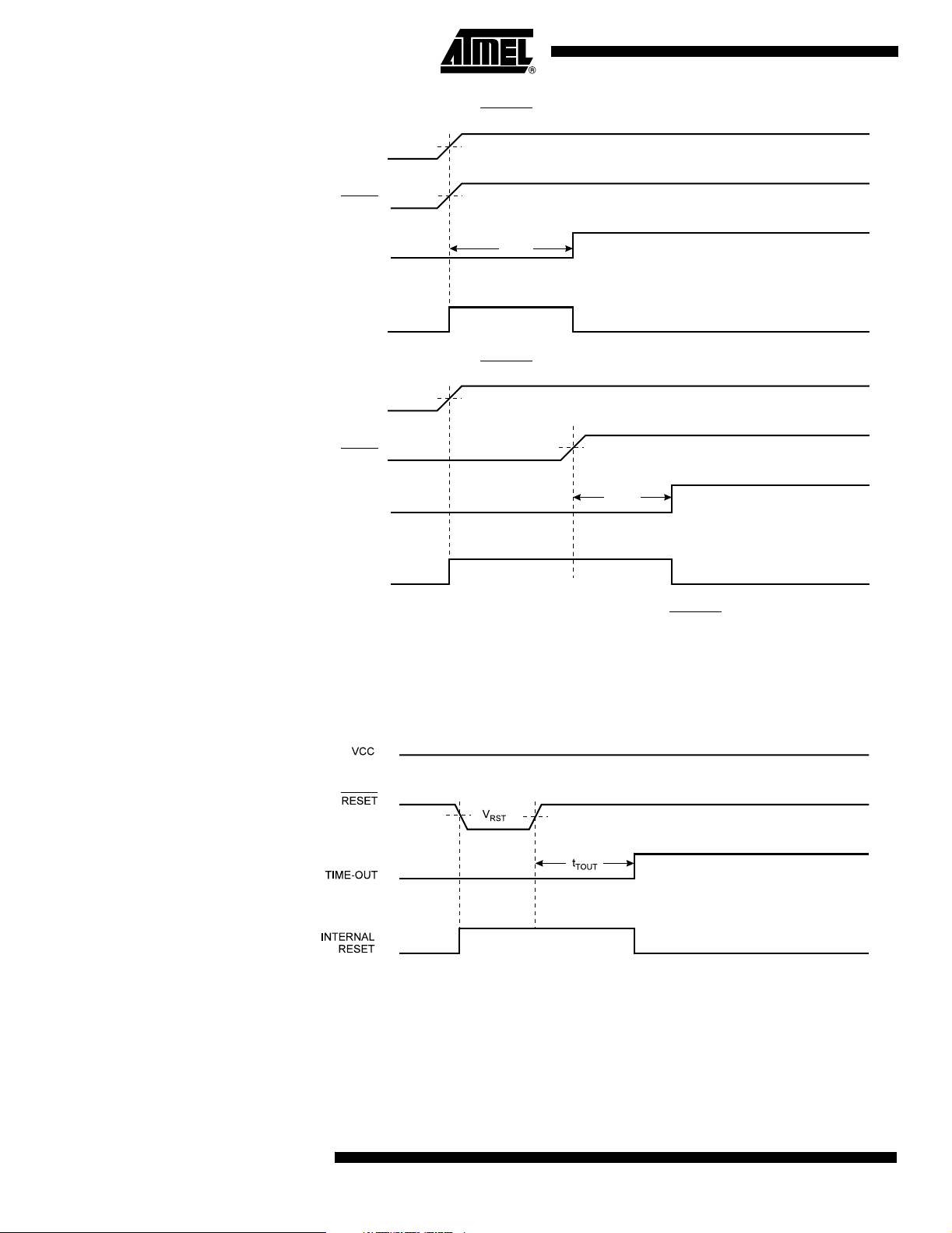
Figure 25. MCU Start-up, RESET Tied to V
V
VCC
RESET
TIME-OUT
INTERNAL
RESET
POT
V
RST
t
TOUT
CC
Figure 26. MCU Start-up, RESET Controlled Externally
V
VCC
RESET
TIME-OUT
INTERNAL
RESET
POT
V
RST
t
TOUT
External Reset An External Reset is generated by a low level on the RESET
than 50 ns will generate a Reset, even if the clock is not running. Shorter pulses are not
guaranteed to generate a Reset. When the applied signal reaches the Reset Threshold
Voltage (V
period (t
) on its positive edge, the delay timer starts the MCU after the Time-out
RST
) has expired.
TOUT
Figure 27. External Reset during Operation
pin. Reset pulses longer
24
AT90S/LS4433
1042G–AVR–09/02
Page 25
AT90S/LS4433
Brown-out Detection AT90S4433 has an On-chip Brown-out Detection (BOD) circuit for monitoring the V
level during the operation. The power supply must be decoupled with a 47 nF to 100 nF
capacitor if the BOD function is used. The BOD circuit can be enabled/disabled by the
fuse BODEN. When BODEN is enabled (BODEN programmed), and V
decreases to a
CC
value below the trigger level, the Brown-out Reset is immediately activated. When V
increases above the trigger level, the Brown-out Reset is deactivated after a delay. The
delay is defined by the user in the same way as the delay of POR signal (see Table 5).
The trigger level for the BOD can be selected by the fuse BODLEVEL to be 2.7V
(BODLEVEL unprogrammed), or 4.0V (BODLEVEL programmed). The trigger level has
a hysteresis of 50 mV to ensure spike-free Brown-out Detection.
The BOD circuit will only detect a drop in V
if the voltage stays below the trigger level
CC
for longer than 3 µs for trigger level 4.0V, 7 µs for trigger level 2.7V (typical values).
Figure 28. Brown-out Reset during Operation
VCC
RESET
TIME-OUT
INTERNAL
RESET
V
BOT-
V
BOT+
t
TOUT
CC
CC
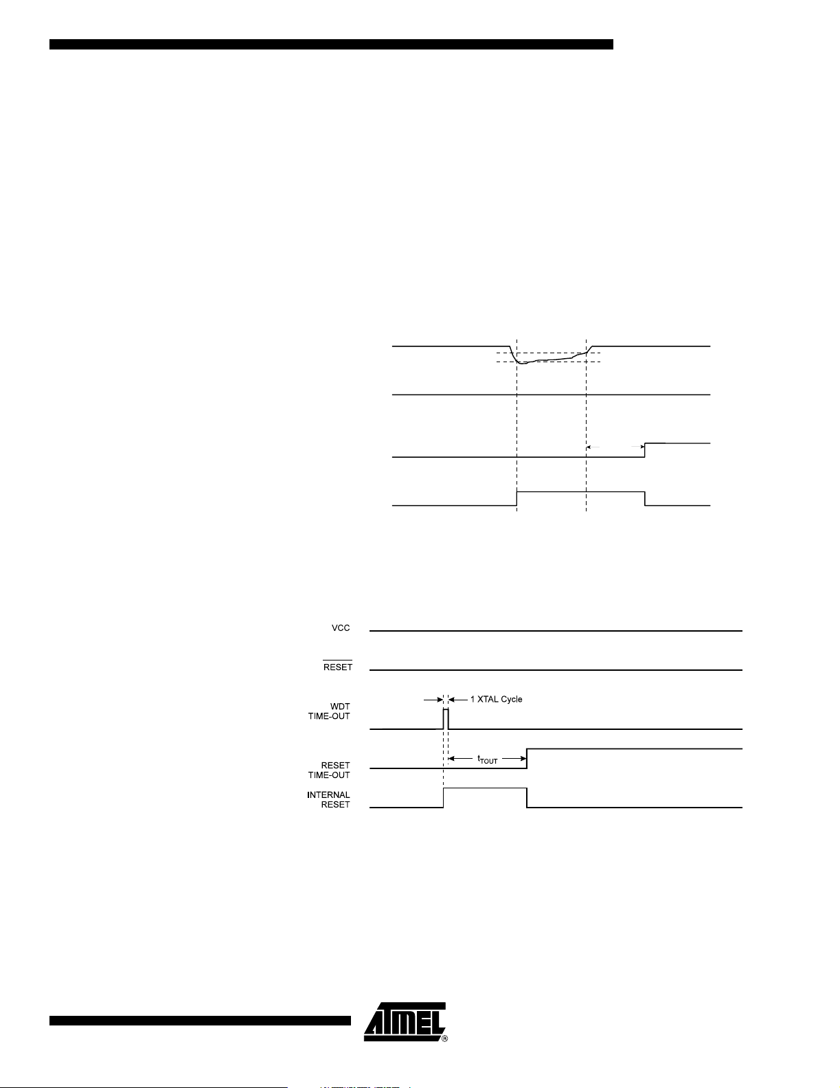
Watchdog Reset When the Watchdog times out, it will generate a short reset pulse of one XTAL cycle
duration. On the falling edge of this pulse, the delay timer starts counting the Time-out
period (t
). See page 43 for details on operation of the Watchdog.
TOUT
Figure 29. Watchdog Reset during Operation
1042G–AVR–09/02
25
Page 26

MCU Status Register – MCUSR
The MCU Status Register provides information on which reset source caused an MCU
Reset.
Bit 76543210
$34 ($54) ––––WDRF BORF EXTRF PORF MCUSR
Read/Write R R R R R/W R/W R/W R/W
Initial Value 0 0 0 0 See Bit Description
• Bits 7..4 – Res: Reserved Bits
These bits are reserved bits in the AT90S4433 and always read as zero.
• Bit 3 – WDRF: Watchdog Reset Flag
This bit is set if a Watchdog Reset occurs. The bit is cleared by a Power-On Reset, or by
writing a logical “0” to the flag.
• Bit 2 – BORF: Brown-out Reset Flag
This bit is set if a Brown-out Reset occurs. The bit is cleared by a Power-on Reset, or by
writing a logical “0” to the flag.
• Bit 1 – EXTRF: External Reset Flag
This bit is set if an External Reset occurs. The bit is cleared by a Power-on Reset, or by
writing a logical “0” to the flag.
• Bit 0 – PORF: Power-on Reset Flag
This bit is set if a Power-on Reset occurs. The bit is cleared only by writing a logical “0”
to the flag.
To make use of the Reset Flags to identify a reset condition, the user should read and
then clear the MCUSR as early as possible in the program. If the register is cleared
before another reset occurs, the source of the reset can be found by examining the
Reset Flags.
Interrupt Handling The AT90S4433 has two 8-bit Interrupt Mask Control Registers; GIMSK (General Inter-
rupt Mask) Register and TIMSK (Timer/Counter Interrupt Mask) Register.
When an interrupt occurs, the Global Interrupt Enable I-bit is cleared (zero) and all interrupts are disabled. The user software can set (one) the I-bit to enable nested interrupts.
The I-bit is set (one) when a Return from Interrupt instruction (RETI) is executed.
When the Program Counter is vectored to the actual Interrupt Vector in order to execute
the interrupt handling routine, hardware clears the corresponding flag that generated the
interrupt. Some of the interrupt flags can also be cleared by writing a logical “1” to the
flag bit position(s) to be cleared.
If an interrupt condition occurs when the corresponding interrupt enable bit is cleared
(zero), the Interrupt Flag will be set and remembered until the interrupt is enabled or the
flag is cleared by software.
If one or more interrupt conditions occur when the Global Interrupt Enable bit is cleared
(zero), the corresponding Interrupt Flag(s) will be set and remembered until the Global
Interrupt Enable bit is set (one), and will be executed by order of priority.
26
Note that external level interrupt does not have a flag and will only be remembered for
as long as the interrupt condition is active.
AT90S/LS4433
1042G–AVR–09/02
Page 27

General Interrupt Mask Register – GIMSK
AT90S/LS4433
Note that the Status Register is not automatically stored when entering an interrupt routine or restored when returning from an interrupt routine. This must be handled by
software.
Bit 7 6 5 4 3 2 1 0
$3B ($5B) INT1 INT0 –– ––––GIMSK
Read/Write R/W R/W R R R R R R
Initial Value 0 0 0 0 0 0 0 0
• Bit 7 – INT1: External Interrupt Request 1 Enable
When the INT1 bit is set (one) and the I-bit in the Status Register (SREG) is set (one),
the external pin interrupt is enabled. The Interrupt Sense Control1 bits 1/0 (ISC11 and
ISC10) in the MCU General Control Register (MCUCR) defines whether the External
Interrupt is activated on rising or falling edge of the INT1 pin or is level sensed. Please
note that INTF1 Flag is not set when the level-sensitive interrupt condition is met. However, INT1 interrupt is generated, provided that INT1 mask bit is set in GIMSK Register.
Activity on the pin will cause an interrupt request even if INT1 is configured as an output.
The corresponding interrupt of External Interrupt Request 1 is executed from program
memory address $002. See also “External Interrupts”.
General Interrupt Flag Register – GIFR
• Bit 6 – INT0: External Interrupt Request 0 Enable
When the INT0 bit is set (one) and the I-bit in the Status Register (SREG) is set (one),
the external pin interrupt is enabled. The Interrupt Sense Control0 bits 1/0 (ISC01 and
ISC00) in the MCU General Control Register (MCUCR) defines whether the External
Interrupt is activated on rising or falling edge of the INT0 pin or is level sensed. Please
note that INTF0 Flag is not set when the level-sensitive interrupt condition is met. However, INT0 interrupt is generated, provided that INT0 mask bit is set in GIMSK Register.
Activity on the pin will cause an interrupt request even if INT0 is configured as an output.
The corresponding interrupt of External Interrupt Request 0 is executed from program
memory address $001. See also “External Interrupts”.
• Bits 5..0 – Res: Reserved Bits
These bits are reserved bits in the AT90S4433 and always read as zero.
Bit 7 6 5 4 3 2 1 0
$3A ($5A) INTF1 INTF0 –– ––––GIFR
Read/Write R/W R/W R R R R R R
Initial Value 0 0 0 0 0 0 0 0
• Bit 7 – INTF1: External Interrupt Flag1
When an edge on the INT1 pin triggers an interrupt request, the corresponding interrupt
flag, INTF1 becomes set (one). If the I-bit in SREG and the corresponding interrupt
enable bit, INT1 in GIMSK, is set (one), the MCU will jump to the Interrupt Vector. The
flag is always cleared when the interrupt routine is executed. Alternatively, the flag is
cleared by writing a logical “1” to it. This flag is always cleared when INT1 is configured
as level interrupt.
1042G–AVR–09/02
27
Page 28

Timer/Counter Interrupt Mask Register – TIMSK
• Bit 6 – INTF0: External Interrupt Flag0
When an edge on the INT0 pin triggers an interrupt request, the corresponding Interrupt
Flag, INTF0 becomes set (one). If the I-bit in SREG and the corresponding interrupt
enable bit, INT0 in GIMSK is set (one), the MCU will jump to the Interrupt Vector. The
flag is always cleared when the interrupt routine is executed. Alternatively, the flag is
cleared by writing a logical “1” to it. This flag is always cleared when INT0 is configured
as level interrupt.
• Bits 5..0 – Res: Reserved Bits
These bits are reserved bits in the AT90S4433 and always read as zero.
Bit 7 6 5 4 3 2 1 0
$39 ($59) TOIE1 OCIE1 ––TICIE1 – TOIE 0 – TIMSK
Read/Write R/W R/W R R R/W R R/W R
Initial Value 0 0 0 0 0 0 0 0
• Bit 7 – TOIE1: Timer/Counter1 Overflow Interrupt Enable
When the TOIE1 bit is set (one) and the I-bit in the Status Register is set (one), the
Timer/Counter1 Overflow Interrupt is enabled. The corresponding interrupt (at vector
$005) is executed if an overflow in Timer/Counter1 occurs, i.e., when the TOV1 bit is set
in the Timer/Counter Interrupt Flag Register (TIFR).
• Bit 6 – OCIE1: Timer/Counter1 Output Compare Match Interrupt Enable
When the OCIE1 bit is set (one) and the I-bit in the Status Register is set (one), the
Timer/Counter1 Compare Match Interrupt is enabled. The corresponding interrupt (at
vector $004) is executed if a compare match in Timer/Counter1 occurs, i.e., when the
OCF1 bit is set in the Timer/Counter Interrupt Flag Register (TIFR).
• Bits 5, 4 – Res: Reserved Bits
These bits are reserved bits in the AT90S4433 and always read as zero.
• Bit 3 – TICIE1: Timer/Counter1 Input Capture Interrupt Enable
When the TICIE1 bit is set (one) and the I-bit in the Status Register is set (one), the
Timer/Counter1 Input Capture Event Interrupt is enabled. The corresponding interrupt
(at vector $003) is executed if a capture-triggering event occurs on pin 14, PB0 (ICP),
i.e., when the ICF1 bit is set in the Timer/Counter Interrupt Flag Register (TIFR).
• Bit 2 – Res: Reserved Bit
This bit is a reserved bit in the AT90S4433 and always reads as zero.
• Bit 1 – TOIE0: Timer/Counter0 Overflow Interrupt Enable
When the TOIE0 bit is set (one) and the I-bit in the Status Register is set (one), the
Timer/Counter0 Overflow Interrupt is enabled. The corresponding interrupt (at vector
$006) is executed if an overflow in Timer/Counter0 occurs, i.e., when the TOV0 bit is set
in the Timer/Counter Interrupt Flag Register (TIFR).
28
• Bit 0 – Res: Reserved Bit
This bit is a reserved bit in the AT90S4433 and always reads as zero.
AT90S/LS4433
1042G–AVR–09/02
Page 29

Timer/Counter Interrupt Flag Register – TIFR
AT90S/LS4433
Bit 7 6 5 4 3 2 1 0
$38 ($58) TO V1 OCF 1 ––ICF1 – TOV0 – TIFR
Read/Write R/W R/W R R R/W R R/W R
Initial Value 0 0 0 0 0 0 0 0
• Bit 7 – TOV1: Timer/Counter1 Overflow Flag
The TOV1 is set (one) when an overflow occurs in Timer/Counter1. TOV1 is cleared by
hardware when executing the corresponding interrupt handling vector. Alternatively,
TOV1 is cleared by writing a logical “1” to the flag. When the I-bit in SREG and TOIE1
(Timer/Counter1 Overflow Interrupt Enable) and TOV1 are set (one), the
Timer/Counter1 Overflow Interrupt is executed. In PWM mode, this bit is set when
Timer/Counter1 advances from $0000.
• Bit 6 – OCF1: Output Compare Flag 1
The OCF1 bit is set (one) when a Compare Match occurs between the Timer/Counter1
and the data in Output Compare Register 1 (OCR1). OCF1 is cleared by hardware when
executing the corresponding interrupt handling vector. Alternatively, OCF1 is cleared by
writing a logical “1” to the flag. When the I-bit in SREG and OCIE1 (Timer/Counter1
Compare Match Interrupt A Enable) and the OCF1 are set (one), the Timer/Counter1
Compare Match Interrupt is executed.
• Bits 5, 4 – Res: Reserved Bits
These bits are reserved bits in the AT90S4433 and always read as zero.
• Bit 3 – ICF1: Input Capture Flag 1
The ICF1 bit is set (one) to flag an Input Capture Event, indicating that the
Timer/Counter1 value has been transferred to the Input Capture Register (ICR1). ICF1
is cleared by hardware when executing the corresponding interrupt handling vector.
Alternatively, ICF1 is cleared by writing a logical “1” to the flag. When the SREG I-bit
and TICIE1 (Timer/Counter1 Input Capture Interrupt Enable) and ICF1 are set (one), the
Timer/Counter1 Capture Interrupt is executed.
• Bit 2 – Res: Reserved Bit
This bit is a reserved bit in the AT90S4433 and always reads as zero.
• Bit 1 – TOV0: Timer/Counter0 Overflow Flag
The bit TOV0 is set (one) when an overflow occurs in Timer/Counter0. TOV0 is cleared
by hardware when executing the corresponding interrupt handling vector. Alternatively,
TOV0 is cleared by writing a logical “1” to the flag. When the SREG I-bit and TOIE0
(Timer/Counter0 Overflow Interrupt Enable) and TOV0 are set (one), the
Timer/Counter0 Overflow Interrupt is executed.
• Bit 0 – Res: Reserved Bit
1042G–AVR–09/02
This bit is a reserved bit in the AT90S4433 and always reads as zero.
29
Page 30

External Interrupts The External Interrupts are triggered by the INT1 and INT0 pins. Observe that, if
enabled, the interrupts will trigger even if the INT0/INT1 pins are configured as outputs.
This feature provides a way of generating a software interrupt. The External Interrupts
can be triggered by a falling or rising edge or a low level. This is set up as indicated in
the specification for the MCU Control Register (MCUCR). When the External Interrupt is
enabled and is configured as level triggered, the interrupt will trigger as long as the pin is
held low.
The External Interrupts are set up as described in the specification for the MCU Control
Register (MCUCR).
Interrupt Response Time The interrupt execution response for all the enabled AVR interrupts is four clock cycles
minimum. Four clock cycles after the Interrupt Flag has been set, the Program Vector
address for the actual interrupt handling routine is executed. During this four clock cycle
period, the Program Counter (two bytes) is pushed onto the Stack, and the Stack
Pointer is decremented by two. The vector is normally a relative jump to the interrupt
routine, and this jump takes two clock cycles. If an interrupt occurs during execution of a
multi-cycle instruction, this instruction is completed before the interrupt is served.
A return from an interrupt handling routine (same as for a subroutine call routine) takes
four clock cycles. During these four clock cycles, the Program Counter (two bytes) is
popped back from the Stack, the Stack Pointer is incremented by two and the I-flag in
SREG is set. When the AVR exits from an interrupt, it will always return to the main program and execute one more instruction before any pending interrupt is served.
MCU Control Register – MCUCR
The MCU Control Register contains control bits for general MCU functions.
Bit 76543210
$35 ($55) ––SE SM ISC11 ISC10 ISC01 ISC00 MCUCR
Read/Write R R R/W R/W R/W R/W R/W R/W
InitialValue00000000
• Bits 7, 6 – Res: Reserved Bits
These bits are reserved bits in the AT90S4433 and always read as zero.
• Bit 5 – SE: Sleep Enable
The SE bit must be set (one) to make the MCU enter the sleep mode when the SLEEP
instruction is executed. To avoid having the MCU entering the sleep mode unless it is
the programmer’s purpose, it is recommended that the Sleep Enable SE bit be set just
before the execution of the SLEEP instruction.
• Bit 4 – SM: Sleep Mode
This bit selects between the two available sleep modes. When SM is cleared (zero), Idle
mode is selected as sleep mode. When SM is set (one), Power-down mode is selected
as sleep mode. For details, refer to the paragraph “Sleep Modes” below.
30
AT90S/LS4433
1042G–AVR–09/02
Page 31

AT90S/LS4433
• Bits 3, 2 – ISC11, ISC10: Interrupt Sense Control 1 Bit 1 and Bit 0
The External Interrupt 1 is activated by the external pin INT1 if the SREG I-flag and the
corresponding interrupt mask in the GIMSK are set. The level and edges on the external
INT1 pin that activate the interrupt are defined in Table 7.
Table 7. Interrupt 1 Sense Control
ISC11 ISC10 Description
0 0 The low level of INT1 generates an interrupt request.
0 1 Any logical change on INT1 generates an interrupt request.
1 0 The falling edge of INT1 generates an interrupt request.
1 1 The rising edge of INT1 generates an interrupt request.
The value on the INT1 pin is sampled before detecting edges. If edge or toggle interrupt
is selected, pulses that last longer than one clock period will generate an interrupt.
Shorter pulses are not guaranteed to generate an interrupt. If low-level interrupt is
selected, the low level must be held until the completion of the currently executing
instruction to generate an interrupt.
• Bits 1, 0 – ISC01, ISC00: Interrupt Sense Control 0 Bit 1 and Bit 0
The External Interrupt 0 is activated by the external pin INT0 if the SREG I-flag and the
corresponding interrupt mask are set. The level and edges on the external INT0 pin that
activate the interrupt are defined in Table 8.
Table 8. Interrupt 0 Sense Control
ISC01 ISC00 Description
0 0 The low level of INT0 generates an interrupt request.
0 1 Any logical change on INT0 generates an interrupt request.
1 0 The falling edge of INT0 generates an interrupt request.
1 1 The rising edge of INT0 generates an interrupt request.
The value on the INT0 pin is sampled before detecting edges. If edge or toggle interrupt
is selected, pulses that last longer than one clock period will generate an interrupt.
Shorter pulses are not guaranteed to generate an interrupt. If low-level interrupt is
selected, the low level must be held until the completion of the currently executing
instruction to generate an interrupt.
Sleep Modes To enter the sleep modes, the SE bit in MCUCR must be set (one) and a SLEEP instruc-
tion must be executed. The SM bit in the MCUCR Register selects which sleep mode
(Idle or Power-down) will be activated by the SLEEP instruction. If an enabled interrupt
occurs while the MCU is in a sleep mode, the MCU wakes up, executes the interrupt
routine, and resumes execution from the instruction following SLEEP. The contents of
the Register File and I/O memory are unaltered. If a reset occurs during sleep mode, the
MCU wakes up and executes from the Reset Vector.
1042G–AVR–09/02
Note that if a level-triggered interrupt is used for wake-up from Power-down, the low
level must be held for a time longer than the reset delay Time-out period (t
TOU T
). Other-
wise, the device will not wake up.
31
Page 32

Idle Mode When the SM bit is cleared (zero), the SLEEP instruction forces the MCU into the Idle
mode stopping the CPU but allowing Timer/Counters, Watchdog and the interrupt system to continue operating. This enables the MCU to wake up from external triggered
interrupts as well as internal ones like Timer Overflow interrupt and Watchdog Reset. If
wake-up from the Analog Comparator interrupt is not required, the Analog Comparator
can be powered down by setting the ACD bit in the Analog Comparator Control and Status Register (ACSR). This will reduce power consumption in Idle mode.
Power-down Mode When the SM bit is set (one), the SLEEP instruction forces the MCU into the Power-
down mode. In this mode, the External Oscillator is stopped while the external interrupts
and the Watchdog (if enabled) continue operating. Only an External Reset, a Watchdog
Reset (if enabled) or an external level interrupt can wake up the MCU.
Note that if a level-triggered interrupt is used for wake-up from Power-down mode, the
changed level must be held for a time to wake up the MCU. This makes the MCU less
sensitive to noise. The Wake-up period is equal to the clock-counting part of the Reset
period (see Table 5). The MCU will wake up from Power-down if the input has the
required level for two Watchdog Oscillator cycles. If the wake-up period is shorter than
two Watchdog Oscillator cycles, the MCU will wake up if the input has the required level
for the duration of the Wake-up period. If the wake-up condition disappears before the
wake-up period has expired, the MCU will wake up from Power-down without executing
the corresponding interrupt.
The period of the Watchdog Oscillator is 2.7 µs (nominal) at 3.0V and 25°C. The frequency of the Watchdog Oscillator is voltage dependent as shown in the Electrical
Characteristics section.
When waking up from Power-down mode, a delay from the wake-up condition occurs
until the wake-up becomes effective. This allows the clock to restart and become stable
after having been stopped. The wake-up period is defined by the same CKSEL Fuses
that define the Reset Time-out period.
32
AT90S/LS4433
1042G–AVR–09/02
Page 33

AT90S/LS4433
Timer/Counters The AT90S4433 provides two general purpose Timer/Counters – one 8-bit T/C and one
16-bit T/C. Timer/Counters0 and 1 have individual prescaling selection from the same
10-bit prescaling timer. These Timer/Counters can either be used as a Timer with an
internal clock time base or as a counter with an external pin connection that triggers the
counting.
Timer/Counter Prescaler Figure 30. Prescaler for Timer/Counter0 and 1
TCK1
For Timer/Counters0 and 1, the four different prescaled selections are CK/8, CK/64,
CK/256, and CK/1024, where CK is the Oscillator clock. For the two Timer/Counters0
and 1, external source and stop can also be selected as clock sources.
TCK0
8-bit Timer/Counter0 The 8-bit Timer/Counter0 can select clock source from CK, prescaled CK or an external
pin. In addition, it can be stopped as described in the specification for the
Timer/Counter0 Control Register (TCCR0). The Overflow Status Flag is found in the
Timer/Counter Interrupt Flag Register (TIFR). Control signals are found in the
Timer/Counter0 Control Register (TCCR0). The interrupt enable/disable settings for
Timer/Counter0 are found in the Timer/Counter Interrupt Mask Register (TIMSK).
When Timer/Counter0 is externally clocked, the external signal is synchronized with the
Oscillator frequency of the CPU. To assure proper sampling of the external clock, the
minimum time between two external clock transitions must be at least one internal CPU
clock period. The external clock signal is sampled on the rising edge of the internal CPU
clock.
The 8-bit Timer/Counter0 features both a high resolution and a high-accuracy usage
with the lower prescaling opportunities. Similarly, the high prescaling opportunities make
the Timer/Counter0 useful for lower speed functions or exact timing functions with infrequent actions. Figure 31 shows the block diagram for Timer/Counter0.
1042G–AVR–09/02
33
Page 34

Figure 31. Timer/Counter0 Block Diagram
OCIE1
OCF1
T0
Timer/Counter0 Control Register – TCCR0
Bit 7 6 5 4 3 2 1 0
$33 ($53) –– – – –CS02 CS01 CS00 TCCR0
Read/Write R R R R R R/W R/W R/W
Initial Value 0 0 0 0 0 0 0 0
• Bits 7 – 3 – Res: Reserved Bits
These bits are reserved bits in the AT90S4433 and always read as zero.
• Bits 2, 1, 0 – CS02, CS01, CS00: Clock Select0, Bits 2, 1, and 0
The Clock Select0 bits 2, 1, and 0 define the prescaling source of Timer/Counter0.
Table 9. Clock 0 Prescale Select
CS02 CS01 CS00 Description
0 0 0 Stop, Timer/Counter0 is stopped.
001CK
010CK/8
011CK/64
100CK/256
101CK/1024
34
1 1 0 External Pin T0, falling edge
1 1 1 External Pin T0, rising edge
AT90S/LS4433
1042G–AVR–09/02
Page 35

The Stop condition provides a Timer Enable/Disable function. The prescaled CK modes
are scaled directly from the CK Oscillator clock. If the external pin modes are used for
Timer/Counter0, transitions on PD4/(T0) will clock the counter even if the pin is configured as an output. This feature can give the user software control of the counting.
Timer Counter0 – TCNT0
Bit 76543210
$32 ($52) MSB LSB TCNT0
Read/Write R/W R/W R/W R/W R/W R/W R/W R/W
InitialValue00000000
The Timer/Counter0 is realized as an up-counter with read and write access. If the
Timer/Counter0 is written and a clock source is present, the Timer/Counter0 continues
counting in the clock cycle following the write operation.
16-bit Timer/Counter1 Figure 32 shows the block diagram for Timer/Counter1.
Figure 32. Timer/Counter1 Block Diagram
AT90S/LS4433
1042G–AVR–09/02
T1
The 16-bit Timer/Counter1 can select clock source from CK, prescaled CK or an external pin. In addition, it can be stopped as described in the specification for the
Timer/Counter1 Control Register (TCCR1A). The different Status Flags (Overflow, Compare Match and Capture Event) and control signals are found in the Timer/Counter
35
Page 36

Interrupt Flag Register (TIFR). The interrupt enable/disable settings for Timer/Counter1
are found in the Timer/Counter Interrupt Mask Register (TIMSK).
When Timer/Counter1 is externally clocked, the external signal is synchronized with the
Oscillator frequency of the CPU. To assure proper sampling of the external clock, the
minimum time between two external clock transitions must be at least one internal CPU
clock period. The external clock signal is sampled on the rising edge of the internal CPU
clock.
The 16-bit Timer/Counter1 features both a high resolution and a high-accuracy usage
with the lower prescaling opportunities. Similarly, the high prescaling opportunities
makes the Timer/Counter1 useful for lower speed functions or exact timing functions
with infrequent actions.
The Timer/Counter1 supports an Output Compare function using the Output Compare
Register1 (OCR1) as the data source to be compared to the Timer/Counter1 contents.
The Output Compare functions include optional clearing of the counter on compare
matches and actions on the Output Compare pin 1 on compare matches.
Timer/Counter1 can also be used as a 8-, 9-, or 10-bit Pulse Width Modulator. In this
mode, the counter and the OCR1 Register serve as a glitch-free, stand-alone PWM with
centered pulses. Refer to page 41 for a detailed description of this function.
The Input Capture function of Timer/Counter1 provides a capture of the Timer/Counter1
contents to the Input Capture Register (ICR1), triggered by an external event on the
Input Capture Pin (ICP). The actual capture event settings are defined by the
Timer/Counter1 Control Register (TCCR1). In addition, the Analog Comparator can be
set to trigger the Input Capture. Refer to the section, “The Analog Comparator”,for
details of this. The ICP pin logic is shown in Figure 33.
Figure 33. ICP Pin Schematic Diagram
If the Noise Canceler function is enabled, the actual trigger condition for the capture
event is monitored over four samples, and all four must be equal to activate the Capture
Flag. The input pin signal is sampled at XTAL clock frequency.
36
AT90S/LS4433
1042G–AVR–09/02
Page 37

Timer/Counter1 Control Register A – TCCR1A
AT90S/LS4433
Bit 7 6 5 4 3 2 1 0
$2F ($4F) COM11 COM10 ––––PWM11 PWM10 TCCR1A
Read/Write R/W R/W R R R R R/W R/W
Initial Value 0 0 0 0 0 0 0 0
• Bits 7, 6 – COM11, COM10: Compare Output Mode1, Bits 1, and 0
The COM11 and COM10 control bits determine any output pin action following a
Compare Match in Timer/Counter1. Any output pin actions affect pin OC1 (Output
Compare pin 1). This is an alternative function to an I/O port, and the corresponding
direction control bit must be set (one) to control an output pin. The control configuration
is shown in Table 10.
Table 10. Compare 1 Mode Select
COM11 COM10 Description
0 0 Timer/Counter1 disconnected from output pin OC1
0 1 Toggle the OC1 output line.
1 0 Clear the OC1 output line (to zero).
1 1 Set the OC1 output line (to one).
In PWM mode, these bits have a different function. Refer to Table 11 for a detailed
description.
• Bits 5..2 – Res: Reserved Bits
These bits are reserved bits in the AT90S4433 and always read as zero.
• Bits 1, 0 – PWM11, PWM10: Pulse Width Modulator Select Bits
These bits select PWM operation of Timer/Counter1 as specified in Table 11. This mode
is described on page 41.
Table 11. PWM Mode Select
PWM11 PWM10 Description
0 0 PWM operation of Timer/Counter1 is disabled
0 1 Timer/Counter1 is an 8-bit PWM
1 0 Timer/Counter1 is a 9-bit PWM
1 1 Timer/Counter1 is a 10-bit PWM
1042G–AVR–09/02
37
Page 38

Timer/Counter1 Control Register B – TCCR1B
Bit 76543210
$2E ($4E) ICNC1 ICES1 ––CTC1 CS12 CS11 CS10 TCCR1B
Read/Write R/W R/W R R R/W R/W R/W R/W
InitialValue0000 0000
• Bit 7 – ICNC1: Input Capture1 Noise Canceler (4 CKs)
When the ICNC1 bit is cleared (zero), the Input Capture trigger Noise Canceler function
is disabled. The Input Capture is triggered at the first rising/falling edge sampled on the
ICP (Input Capture Pin) as specified. When the ICNC1 bit is set (one), four successive
samples are measured on the ICP (Input Capture Pin), and all samples must be
high/low according to the input capture trigger specification in the ICES1 bit. The actual
sampling frequency is the XTAL clock frequency.
• Bit 6 – ICES1: Input Capture1 Edge Select
While the ICES1 bit is cleared (zero), the Timer/Counter1 contents are transferred to the
Input Capture Register (ICR1) on the falling edge of the Input Capture Pin (ICP). While
the ICES1 bit is set (one), the Timer/Counter1 contents are transferred to the Input Capture Register (ICR1) on the rising edge of the Input Capture Pin (ICP).
• Bits 5, 4 – Res: Reserved Bits
These bits are reserved bits in the AT90S4433 and always read as zero.
• Bit 3 – CTC1: Clear Timer/Counter1 on Compare Match
When the CTC1 control bit is set (one), the Timer/Counter1 is reset to $0000 in the clock
cycle after a Compare Match. If the CTC1 control bit is cleared, Timer/Counter1 continues counting and is unaffected by a Compare Match. Since the compare match is
detected in the CPU clock cycle following the match, this function will behave differently
when a prescaling higher than 1 is used for the Timer. When a prescaling of 1 is used
and the Compare Register is set to C, the timer will count as follows if CTC1 is set:
...|C-2|C-1|C|0|1|...
When the prescaler is set to divide by 8, the timer will count like this:
... | C-2, C-2, C-2, C-2, C-2, C-2, C-2, C-2 | C-1, C-1, C-1, C-1, C-1, C-1, C-1, C-1 | C, 0,
0, 0, 0, 0, 0, 0 | 1, 1, 1, 1, 1, 1, 1, 1| ...
In PWM mode, this bit has no effect.
38
AT90S/LS4433
1042G–AVR–09/02
Page 39

AT90S/LS4433
• Bits 2, 1, 0 – CS12, CS11, CS10: Clock Select1, Bits 2, 1, and 0
The Clock Select1 bits 2, 1, and 0 define the prescaling source of Timer/Counter1.
Table 12. Clock 1 Prescale Select
CS12 CS11 CS10 Description
0 0 0 Stop, the Timer/Counter1 is stopped.
001CK
010CK/8
011CK/64
100CK/256
1 0 1 CK/1024
1 1 0 External Pin T1, falling edge
1 1 1 External Pin T1, rising edge
The Stop condition provides a Timer Enable/Disable function. The prescaled CK modes
are scaled directly from the CK Oscillator clock. If the external pin modes are used for
Timer/Counter0, transitions on PD5/(T1) will clock the counter even if the pin is configured as an output. This feature can give the user software control of the counting.
Timer/Counter1 – TCNT1H and TCNT1L
Bit 151413121110 9 8
$2D ($4D) MSB TCNT1H
$2C ($4C) LSB TCNT1L
76543210
Read/Write R/W R/W R/W R/W R/W R/W R/W R/W
R/W R/W R/W R/W R/W R/W R/W R/W
InitialValue00000000
00000000
This 16-bit register contains the prescaled value of the 16-bit Timer/Counter1. To
ensure that both the High and Low Bytes are read and written simultaneously when the
CPU accesses these registers, the access is performed using an 8-bit temporary register (TEMP). This temporary register is also used when accessing OCR1 and ICR1. If the
main program and interrupt routines perform access to registers using TEMP, interrupts
must be disabled during access from the main program (and from interrupt routines if
interrupts are allowed from within interrupt routines).
• TCNT1 Timer/Counter1 Write
When the CPU writes to the High Byte TCNT1H, the written data is placed in the TEMP
Register. Next, when the CPU writes the Low Byte TCNT1L, this byte of data is combined with the byte data in the TEMP Register, and all 16 bits are written to the TCNT1
Timer/Counter1 Register simultaneously. Consequently, the High Byte TCNT1H must
be accessed first for a full 16-bit register write operation.
1042G–AVR–09/02
• TCNT1 Timer/Counter1 Read
When the CPU reads the Low Byte TCNT1L, the data of the Low Byte TCNT1L is sent
to the CPU and the data of the High Byte TCNT1H is placed in the TEMP Register.
When the CPU reads the data in the High Byte TCNT1H, the CPU receives the data in
39
Page 40

Timer/Counter1 Output Compare Register – OCR1H and OCR1L
the TEMP Register. Consequently, the Low Byte TCNT1L must be accessed first for a
full 16-bit register read operation.
The Timer/Counter1 is realized as an up or up/down (in PWM mode) counter with read
and write access. If Timer/Counter1 is written to and a clock source is selected, the
Timer/Counter1 continues counting in the timer clock cycle after it is preset with the written value.
Bit 151413121110 9 8
$2B ($4B) MSB OCR1H
$2A ($4A) LSB OCR1L
76543210
Read/Write R/W R/W R/W R/W R/W R/W R/W R/W
R/W R/W R/W R/W R/W R/W R/W R/W
InitialValue00000000
00000000
The Output Compare Register is a 16-bit read/write register.
The Timer/Counter1 Output Compare Register contains the data to be continuously
compared with Timer/Counter1. Actions on compare matches are specified in the
Timer/Counter1 Control and Status Register.
Since the Output Compare Register (OCR1) is a 16-bit register, a temporary register
TEMP is used when OCR1 is written to ensure that both bytes are updated simultaneously. When the CPU writes the High Byte, OCR1H, the data is temporarily stored in
the TEMP Register. When the CPU writes the Low Byte, OCR1L, the TEMP Register is
simultaneously written to OCR1H. Consequently, the High Byte OCR1H must be written
first for a full 16-bit register write operation.
The TEMP Register is also used when accessing TCNT1 and ICR1. If the main program
and interrupt routines perform access to registers using TEMP, interrupts must be disabled during access from the main program.
40
AT90S/LS4433
1042G–AVR–09/02
Page 41

Timer/Counter1 Input Capture Register – ICR1H and ICR1L
AT90S/LS4433
Bit 151413121110 9 8
$27 ($47) MSB ICR1H
$26 ($46) LSB ICR1L
76543210
Read/Write R R RRRRRR
RRRRRRRR
InitialValue00000000
00000000
The Input Capture Register is a 16-bit, read only register.
When the rising or falling edge (according to the input capture edge setting [ICES1]) of
the signal at the Input Capture Pin (ICP) is detected, the current value of the
Timer/Counter1 is transferred to the Input Capture Register (ICR1). At the same time,
the Input Capture Flag (ICF1) is set (one).
Since the Input Capture Register (ICR1) is a 16-bit register, a temporary register
(TEMP) is used when ICR1 is read to ensure that both bytes are read simultaneously.
When the CPU reads the Low Byte, ICR1L, the data is sent to the CPU and the data of
the High Byte, ICR1H, is placed in the TEMP Register. When the CPU reads the data in
the High Byte, ICR1H, the CPU receives the data in the TEMP Register. Consequently,
the Low Byte, ICR1L, must be accessed first for a full 16-bit register read operation.
The TEMP Register is also used when accessing TCNT1 and OCR1. If the main program and interrupt routines perform access to registers using TEMP, interrupts must be
disabled during access from the main program.
Timer/Counter1 in PWM Mode When the PWM mode is selected, Timer/Counter1 and the Output Compare Register1
(OCR1) form a 8-, 9-, or 10-bit, free-running, glitch-free, phase correct PWM with output
on the PB1(OC1) pin. Timer/Counter1 acts as an up/down counter, counting up from
$0000 to TOP (see Table 13), where it turns and counts down again to zero before the
cycle is repeated. When the counter value matches the contents of the 8, 9, or 10 least
significant bits of OCR1, the PB1(OC1) pin is set or cleared according to the settings of
the COM11 and COM10 bits in the Timer/Counter1 Control Register (TCCR1). Refer to
Table 14 for details.
Table 13. Timer TOP Values and PWM Frequency
PWM Resolution Timer TOP Value Frequency
8-bit $00FF (255) f
9-bit $01FF (511) f
10-bit $03FF(1023) f
Note: 1. If the Compare Register contains the TOP value and the prescaler is not in use
(CS12..CS10 = 001), the PWM output will not produce any pulse at all, because the
up-counting and down-counting values are reached simultaneously. When the prescaler is in use (CS12..CS10 ≠ 001 or 000), the PWM output goes active when the
counter reaches the TOP value, but the down-counting compare match is not interpreted to be reached before the next time the counter reaches the TOP value,
making a one-period PWM pulse.
(1)
TCK1
TCK1
TCK1
/510
/1022
/2046
1042G–AVR–09/02
41
Page 42

Table 14. Compare1 Mode Select in PWM Mode
COM11 COM10 Effect on OC1
0 0 Not connected
0 1 Not connected
10
11
Cleared on compare match, up-counting. Set on compare match, downcounting (non-inverted PWM).
Cleared on compare match, down-counting. Set on compare match, upcounting (inverted PWM).
Note that in the PWM mode, the ten least significant OCR1 bits, when written, are transferred to a temporary location. They are latched when Timer/Counter1 reaches TOP.
This prevents the occurrence of odd-length PWM pulses (glitches) in the event of an
unsynchronized OCR1 write. See Figure 34 for an example.
Figure 34. Effects on Unsynchronized OCR1 Latching
During the time between the write and the latch operation, a read from OCR1 will read
the contents of the temporary location. This means that the most recently written value
always will read out of OCR1.
When OCR1 contains $0000 or TOP, the output OC1 is updated to low or high on the
next compare match according to the settings of COM11 and COM10. This is shown in
Table 15.
Table 15. PWM Outputs OCR = $0000 or TOP
COM11 COM10 OCR1 Output OC1
1 0 $0000 L
10TOP H
1 1 $0000 H
11TOP L
In PWM mode, the Timer Overflow Flag1 (TOV1) is set when the counter changes direction at $0000. Timer Overflow Interrupt1 operates exactly as in normal Timer/Counter
mode, i.e., it is executed when TOV1 is set, provided that Timer Overflow Interrupt1 and
global interrupts are enabled. This also applies to the Timer Output Compare1 Flag and
interrupt.
42
AT90S/LS4433
1042G–AVR–09/02
Page 43

AT90S/LS4433
Watchdog Timer The Watchdog Timer is clocked from a separate On-chip Oscillator. By controlling the
Watchdog Timer prescaler, the Watchdog Reset interval can be adjusted as shown in
Table 6. See characterization data for typical values at other V
(Watchdog Reset) instruction resets the Watchdog Timer. Eight different clock cycle
periods can be selected to determine the reset period. If the reset period expires without
another Watchdog Reset, the AT90S4433 resets and executes from the Reset vector.
For timing details on the Watchdog Reset, refer to page 25.
To prevent unintentional disabling of the Watchdog, a special turn-off sequence must be
followed when the Watchdog is disabled. Refer to the description of the Watchdog Timer
Control Register for details.
Figure 35. Watchdog Timer
levels. The WDR
CC
Watchdog Timer Control Register – WDTCR
Bit 76543210
$21 ($41) –––WDTOE WDE WDP2 WDP1 WDP0 WDTCR
Read/Write R R R R/W R/W R/W R/W R/W
Initial Value 0 0 0 0 0 0 0 0
• Bits 7..5 – Res: Reserved Bits
These bits are reserved bits in the AT90S4433 and will always read as zero.
• Bit 4 – WDTOE: Watchdog Turn-off Enable
This bit must be set (one) when the WDE bit is cleared. Otherwise, the Watchdog will
not be disabled. Once set, hardware will clear this bit to zero after four clock cycles.
Refer to the description of the WDE bit for a Watchdog disable procedure.
• Bit 3 – WDE: Watchdog Enable
When the WDE is set (one), the Watchdog Timer is enabled; if the WDE is cleared
(zero), the Watchdog Timer function is disabled. WDE can only be cleared if the
WDTOE bit is set (one). To disable an enabled Watchdog Timer, the following procedure must be followed:
1. In the same operation, write a logical “1” to WDTOE and WDE. A logical “1” must
be written to WDE even though it is set to one before the disable operation
starts.
2. Within the next four clock cycles, write a logical “0” to WDE. This disables the
Watchdog.
1042G–AVR–09/02
43
Page 44

• Bits 2..0 – WDP2, WDP1, WDP0: Watchdog Timer Prescaler 2, 1, and 0
The WDP2, WDP1, and WDP0 bits determine the Watchdog Timer prescaling when the
Watchdog Timer is enabled. The different prescaling values and their corresponding
time-out periods are shown inTable 16.
Table 16. Watchdog Timer Prescale Select
Number of WDT
WDP2 WDP1 WDP0
0 0 0 16K cycles 47 ms 15 ms
0 0 1 32K cycles 94 ms 30 ms
0 1 0 64K cycles 0.19 s 60 ms
0 1 1 128K cycles 0.38 s 0.12 s
1 0 0 256K cycles 0.75 s 0.24 s
1 0 1 512K cycles 1.5 s 0.49 s
1 1 0 1,024K cycles 3.0 s 0.97 s
1 1 1 2,048K cycles 6.0 s 1.9 s
Note: 1. The frequency of the Watchdog Oscillator is voltage dependent, as shown in the
Electrical Characteristics section.
The WDR (Watchdog Reset) instruction should always be executed before the
Watchdog Timer is enabled. This ensures that the reset period will be in accordance
with the Watchdog Timer prescale settings. If the Watchdog Timer is enabled without
reset, the Watchdog Timer may not start counting from zero.
To avoid unintentional MCU reset, the Watchdog Timer should be disabled or Reset
before changing the Watchdog Timer Prescale Select.
Oscillator Cycles
(1)
Typical Time-out
at VCC=3.0V
Typical Time-out
at VCC=5.0V
44
AT90S/LS4433
1042G–AVR–09/02
Page 45

AT90S/LS4433
EEPROM Read/Write Access
EEPROM Address Register – EEAR
The EEPROM Access Registers are accessible in the I/O space.
The write access time is in the range of 2.5 - 4 ms, depending on the V
voltages. A
CC
self-timing function lets the user software detect when the next byte can be written. A
special EEPROM Ready interrupt can be set to trigger when the EEPROM is ready to
accept new data.
An ongoing EEPROM write operation will complete even if a reset condition occurs.
In order to prevent unintentional EEPROM writes, a two-state write procedure must be
followed. Refer to the description of the EEPROM Control Register for details on this.
When the EEPROM is written, the CPU is halted for two clock cycles before the next
instruction is executed.
When the EEPROM is read, the CPU is halted for four clock cycles before the next
instruction is executed.
Bit 76543210
$1E ($3E) EEAR7 EEAR6 EEAR5 EEAR4 EEAR3 EEAR2 EEAR1 EEAR0 EE AR
Read/Write R/W R/W R/W R/W R/W R/W R/W R/W
InitialValueXXXXXXXX
The EEPROM Address Register (EEAR) specifies the EEPROM address in the 256
bytes of EEPROM space. The EEPROM data bytes are addressed linearly between 0
and 255. The Initial Value of EEAR is undefined. A proper value must be written before
the EEPROM may be accessed.
EEPROM Data Register – EEDR
EEPROM Control Register – EECR
Bit 76543210
$1D ($3D) MSB LSB EEDR
Read/Write R/W R/W R/W R/W R/W R/W R/W R/W
InitialValue00000000
• Bits 7..0 – EEDR7.0: EEPROM Data
For the EEPROM write operation, the EEDR Register contains the data to be written to
the EEPROM in the address given by the EEAR Register. For the EEPROM read operation, the EEDR contains the data read out from the EEPROM at the address given by
EEAR.
Bit 76543210
$1C ($3C) ––––EERIE EEMWE EEW E EERE EECR
Read/Write R R R R R/W R/W R/W R/W
InitialValue00000000
• Bits 7..4 – Res: Reserved Bits
These bits are reserved bits in the AT90S4433 and will always read as zero.
1042G–AVR–09/02
45
Page 46

• Bit 3 – EERIE: EEPROM Ready Interrupt Enable
When the I-bit in SREG and EERIE are set (one), the EEPROM Ready Interrupt is
enabled. When cleared (zero), the interrupt is disabled. The EEPROM Ready Interrupt
generates a constant interrupt when EEWE is cleared (zero).
• Bit 2 – EEMWE: EEPROM Master Write Enable
The EEMWE bit determines whether setting EEWE to one causes the EEPROM to be
written. When EEMWE is set (one), setting EEWE will write data to the EEPROM at the
selected address. If EEMWE is zero, setting EEWE will have no effect. When EEMWE
has been set (one) by software, hardware clears the bit to zero after four clock cycles.
See the description of the EEWE bit for a EEPROM write procedure.
• Bit 1 – EEWE: EEPROM Write Enable
The EEPROM Write Enable Signal (EEWE) is the write strobe to the EEPROM. When
address and data are correctly set up, the EEWE bit must be set to write the value into
the EEPROM. The EEMWE bit must be set when the logical “1” iswrittentoEEWE,otherwise no EEPROM write takes place. The following procedure should be followed
when writing the EEPROM (the order of steps 2 and 3 is unessential):
1. Wait until EEWE becomes zero.
2. Write new EEPROM address to EEAR (optional).
3. Write new EEPROM data to EEDR (optional).
4. Write a logical “1” to the EEMWE bit in EECR (to be able to write a logical “1” to
theEEMWEbit,theEEWEbitmustbewrittentozerointhesamecycle).
5. Within four clock cycles after setting EEMWE, write a logical “1” to EEWE.
Caution: An interrupt between step 4 and step 5 will make the write cycle fail, since the
EEPROM Master Write Enable will time-out. If an interrupt routine accessing the
EEPROM is interrupting another EEPROM access, the EEAR and EEDR Registers will
be modified, causing the interrupted EEPROM access to fail. It is recommended to have
the global interrupt flag cleared during the last four steps to avoid these problems.
When the write access time (typically 2.5 ms at V
elapsed, the EEWE bit is cleared (zero) by hardware. The user software can poll this bit
and wait for a zero before writing the next byte. When EEWE has been set, the CPU is
halted for two cycles before the next instruction is executed.
• Bit 0 – EERE: EEPROM Read Enable
The EEPROM Read Enable Signal (EERE) is the read strobe to the EEPROM. When
the correct address is set up in the EEAR Register, the EERE bit must be set. When the
EERE bit is cleared (zero) by hardware, requested data is found in the EEDR Register.
The EEPROM read access takes one instruction and there is no need to poll the EERE
bit. When EERE has been set, the CPU is halted for four cycles before the next instruction is executed.
The user should poll the EEWE bit before starting the read operation. If a write operation
is in progress when new data or address is written to the EEPROM I/O Registers, the
write operation will be interrupted and the result is undefined.
=5Vor4msatVCC=2.7V)has
CC
46
AT90S/LS4433
1042G–AVR–09/02
Page 47

AT90S/LS4433
Prevent EEPROM Corruption
During periods of low VCC, the EEPROM data can be corrupted because the supply voltage is too low for the CPU and the EEPROM to operate properly. These issues are the
same as for board-level systems using the EEPROM, and the same design solutions
should be applied.
An EEPROM data corruption can be caused by two situations when the voltage is too
low. First, a regular write sequence to the EEPROM requires a minimum voltage to
operate correctly. Second, the CPU itself can execute instructions incorrectly if the supply voltage for executing instructions is too low.
EEPROM data corruption can easily be avoided by following these design recommendations (one is sufficient):
1. Keep the AVR RESET active (low) during periods of insufficient power supply
voltage. This can be done by enabling the internal Brown-out Detector (BOD) if
the operating speed matches the detection level. If not, an external low V
Reset Protection circuit can be applied.
2. Keep the AVR core in Power-down sleep mode during periods of low V
will prevent the CPU from attempting to decode and execute instructions, effectively protecting the EEPROM Registers from unintentional writes.
3. Store constants in Flash memory if the ability to change memory contents from
software is not required. Flash memory cannot be updated by the CPU and will
not be subject to corruption.
CC
CC
.This
1042G–AVR–09/02
47
Page 48

Serial Peripheral Interface – SPI
The Serial Peripheral Interface (SPI) allows high-speed synchronous data transfer
between the AT90S4433 and peripheral devices or between several AVR devices. The
AT90S4433 SPI features include the following:
•
Full Duplex, Three-wire Synchronous Data Transfer
• Master or Slave Operation
• LSB First or MSB First Data Transfer
• Four Programmable Bit Rates
• End of Transmission Interrupt Flag
• Write Collision Flag Protection
• Wake-up from Idle Mode
Figure 36. SPI Block Diagram
48
The interconnection between Master and Slave CPUs with SPI is shown in Figure 37.
The PB5(SCK) pin is the clock output in the Master mode and is the clock input in the
Slave mode. Writing to the SPI Data Register of the Master CPU starts the SPI clock
generator, and the data written shifts out of the PB3(MOSI) pin and into the PB3(MOSI)
pin of the Slave CPU. After shifting one byte, the SPI clock generator stops, setting the
end of Transmission Flag (SPIF). If the SPI Interrupt Enable bit (SPIE) in the SPCR
Register is set, an interrupt is requested. The Slave Select input, PB2(SS
select an individual Slave SPI device. The two Shift Registers in the Master and the
Slave can be considered as one distributed 16-bit circular Shift Register. This is shown
in Figure 37. When data is shifted from the Master to the Slave, data is also shifted in
the opposite direction, simultaneously. This means that during one shift cycle, data in
the master and the slave are interchanged.
AT90S/LS4433
), is set low to
1042G–AVR–09/02
Page 49

AT90S/LS4433
Figure 37. SPI Master-slave Interconnection
The system is single buffered in the transmit direction and double buffered in the receive
direction. This means that bytes to be transmitted cannot be written to the SPI Data
Register before the entire shift cycle is completed. When receiving data, however, a
received byte must be read from the SPI Data Register before the next byte has been
completely shifted in. Otherwise, the first byte is lost.
When the SPI is enabled, the data direction of the MOSI, MISO, SCK, and SS
pins is
overridden according to Table 17.
Table 17. SPI Pin Direction Overrides
Pin Direction Overrides, Master SPI Mode Direction Overrides, Slave SPI Modes
MOSI User Defined Input
MISO Input User Defined
SCK User Defined Input
SS
User Defined Input
Note: 1. See “Alternate Functions of Port B” on page 73 for a detailed description of how to
define the direction of the user-defined SPI pins.
(1)
SS Pin Functionality When the SPI is configured as a Master (MSTR in SPCR is set), the user can determine
the direction of the SS
pin, which does not affect the SPI system. If SS
high to ensure Master SPI operation. If the SS
when the SPI is configured as master with the SS
tem interprets this as another master selecting the SPI as a slave and starts to send
data to it. To avoid bus contention, the SPI system takes the following actions:
1. The MSTR bit in SPCR is cleared and the SPI system becomes a Slave. As a
result of the SPI becoming a Slave, the MOSI and SCK pins become inputs.
2. The SPIF Flag in SPSR is set, and if the SPI interrupt is enabled and the I-bit in
SREG is set, the interrupt routine will be executed.
pin. If SS is configured as an output, the pin is a general output
is configured as an input, it must be held
pin is driven low by peripheral circuitry
pin defined as an input, the SPI sys-
1042G–AVR–09/02
Thus, when interrupt-driven SPI transmittal is used in Master mode, and there exists a
possibility that SS
is driven low, the interrupt should always check that the MSTR bit is
still set. Once the MSTR bit has been cleared by a slave select, it must be set by the
user to re-enable the SPI Master mode.
When the SPI is configured as a slave, the SS
pin is always input. When SS is held low,
the SPI is activated and MISO becomes an output if configured so by the user. All other
49
Page 50

pins are inputs. When SS is driven high, externally all pins are inputs and the SPI is
passive, which means that it will not receive incoming data. Note that the SPI logic will
be reset once the SS
transmission, the SPI will stop sending and receiving immediately and both data
received and data sent must be considered as lost.
pin is brought high. If the SS pin is brought high during a
Data Modes There are four combinations of SCK phase and polarity with respect to serial data,
which are determined by control bits CPHA and CPOL. The SPI data transfer formats
are shown in Figure 38 and Figure 39.
Figure 38. SPI Transfer Format with CPHA = 0 and DORD = 0
Figure 39. SPI Transfer Format with CPHA = 1 and DORD = 0
50
AT90S/LS4433
1042G–AVR–09/02
Page 51

SPIControlRegister– SPCR
AT90S/LS4433
Bit 76543210
$0D ($2D) SPIE SPE DORD MSTR CPOL CPHA SPR1 SPR0 SPCR
Read/Write R/W R/W R/W R/W R/W R/W R/W R/W
InitialValue00000000
• Bit 7 – SPIE: SPI Interrupt Enable
This bit causes the SPI interrupt to be executed if SPIF bit in the SPSR Register is set
and the global interrupts are enabled.
• Bit 6 – SPE: SPI Enable
When the SPE bit is set (one), the SPI is enabled. This bit must be set to enable any SPI
operations.
• Bit 5 – DORD: Data Order
When the DORD bit is set (one), the LSB of the data word is transmitted first.
When the DORD bit is cleared (zero), the MSB of the data word is transmitted first.
• Bit 4 – MSTR: Master/Slave Select
This bit selects Master SPI mode when set (one), and Slave SPI mode when cleared
(zero). If SS
is configured as an input and is driven low while MSTR is set, MSTR will be
cleared and SPIF in SPSR will become set. The user will then have to set MSTR to reenable SPI Master mode.
• Bit 3 – CPOL: Clock Polarity
When this bit is set (one), SCK is high when idle. When CPOL is cleared (zero), SCK is
low when idle. Refer to Figure 38 and Figure 39 for additional information.
• Bit 2 – CPHA: Clock Phase
Refer to Figure 38 or Figure 39 for the functionality of this bit.
• Bits 1, 0 – SPR1, SPR0: SPI Clock Rate Select 1 and 0
These two bits control the SCK rate of the device configured as a Master. SPR1 and
SPR0 have no effect on the Slave. The relationship between SCK and the Oscillator
clock frequency (f
) is shown in Table 18.
cl
Table 18. Relationship between SCK and the Oscillator Frequency
SPR1 SPR0 SCK Frequency
00 f
01 f
10 f
11 f
cl
cl
cl
/128
cl
/4
/16
/64
1042G–AVR–09/02
51
Page 52

SPI Status Register – SPSR
Bit 76543210
$0E ($2E) SPIF WCOL ––––––SPSR
Read/Write R RRRRRRR
InitialValue00000000
• Bit 7 – SPIF: SPI Interrupt Flag
When a serial transfer is complete, the SPIF bit is set (one) and an interrupt is generated if SPIE in SPCR is set (one) and global interrupts are enabled. If SS
is an input and
is driven low when the SPI is in Master mode, this will also set the SPIF Flag. SPIF is
cleared by hardware when executing the corresponding interrupt handling vector. Alternatively, the SPIF bit is cleared by first reading the SPI Status Register with SPIF set
(one), then by accessing the SPI Data Register (SPDR).
• Bit 6 – WCOL: Write Collision Flag
The WCOL bit is set if the SPI Data Register (SPDR) is written during a data transfer.
The WCOL bit (and the SPIF bit) are cleared (zero) by first reading the SPI Status Register with WCOL set (one), and then by accessing the SPI Data Register.
• Bits 5..0 – Res: Reserved Bits
These bits are reserved bits in the AT90S4433 and will always read as zero.
The SPI interface on the AT90S4433 is also used for Program memory and EEPROM
downloading or uploading. See page 93 for Serial Programming and verification.
SPI Data Register – SPDR
Bit 76543210
$0F ($2F) MSB LSB SPDR
Read/Write R/W R/W R/W R/W R/W R/W R/W R/W
InitialValueXXXXXXXXUndefined
The SPI Data Register is a read/write register used for data transfer between the Register File and the SPI Shift Register. Writing to the register initiates data transmission.
Reading the register causes the Shift Register Receive buffer to be read.
52
AT90S/LS4433
1042G–AVR–09/02
Page 53

AT90S/LS4433
UART The AT90S4433 features a full duplex (separate Receive and Transmit Registers) Uni-
versal Asynchronous Receiver and Transmitter (UART). The main features are:
•
Baud Rate Generator Generates any Baud Rate
• High Baud Rates at Low XTAL Frequencies
• 8 or 9 Bits Data
• Noise Filtering
• Overrun Detection
• Framing Error Detection
• False Start Bit Detection
• Three Separate Interrupts on TX Complete, TX Data Register Empty, and RX Complete
• Multi-processor Communication Mode
Data Transmission A block schematic of the UART Transmitter is shown in Figure 40.
Figure 40. UART Transmitter
UART CONTROL
AND STAUS
REGISTER B (UCSRB)
UART CONTROL
AND STAUS
REGISTER A (UCSRA)
Data transmission is initiated by writing the data to be transmitted to the UART I/O Data
Register (UDR). Data is transferred from UDR to the Transmit Shift Register when:
• A new character has been written to UDR after the stop bit from the previous
character has been shifted out. The Shift Register is loaded immediately.
• A new character has been written to UDR before the stop bit from the previous
character has been shifted out. The Shift Register is loaded when the stop bit of the
character currently being transmitted has been shifted out.
When data is transferred from UDR to the Shift Register, the UDRE (UART Data Register Empty) bit in the UART Control and Status Register A, UCSRA, is set. When this bit
is set (one), the UART is ready to receive the next character. At the same time as the
1042G–AVR–09/02
53
Page 54

data is transferred from UDR to the 10(11)-bit Shift Register, bit 0 of the Shift Register is
cleared (start bit) and bit 9 or 10 is set (stop bit). If 9-bit data word is selected (the CHR9
bit in the UART Control and Status Register B, UCSRB is set), the TXB8 bit in UCSRB is
transferred to bit nine in the Transmit Shift Register.
On the baud rate clock following the transfer operation to the Shift Register, the start bit
is shifted out on the TXD pin. Then follows the data, LSB first. When the stop bit has
been shifted out, the Shift Register is loaded if any new data has been written to the
UDR during the transmission. During loading, UDRE is set. If there is no new data in the
UDR Register to send when the stop bit is shifted out, the UDRE Flag will remain set
until UDR is written again. When no new data has been written, and the stop bit has
been present on TXD for one bit length, the TX Complete Flag, TXC, in UCSRA is set.
The TXEN bit in UCSRB enables the UART Transmitter when set (one). When this bit is
cleared (zero), the PD1 pin can be used for general I/O. When TXEN is set, the UART
Transmitter will be connected to PD1, which is forced to be an output pin regardless of
the setting of the DDD1 bit in DDRD.
Data Reception Figure 41 shows a block diagram of the UART Receiver.
Figure 41. UART Receiver
54
AT90S/LS4433
UART CONTROL
AND STAUS
REGISTER A (UCSRA)
UART CONTROL
AND STAUS
REGISTER B (UCSRB)
1042G–AVR–09/02
Page 55

AT90S/LS4433
The Receiver front-end logic samples the signal on the RXD pin at a frequency 16 times
the baud rate. While the line is idle, one single sample of logical “0” will be interpreted as
the falling edge of a start bit, and the start bit detection sequence is initiated. Let sample
1 denote the first zero-sample. Following the 1-to-0 transition, the Receiver samples the
RXD pin at samples 8, 9, and 10. If two or more of these three samples are found to be
logical “1”s, the start bit is rejected as a noise spike and the receiver starts looking for
the next 1-to-0 transition.
If, however, a valid start bit is detected, sampling of the data bits following the start bit is
performed. These bits are also sampled at samples 8, 9, and 10. The logical value found
in at least two of the three samples is taken as the bit value. All bits are shifted into the
transmitter Shift Register as they are sampled. Sampling of an incoming character is
shown in Figure 42.
Figure 42. Sampling Received Data
When the stop bit enters the receiver, the majority of the three samples must be one to
accept the stop bit. If two or more samples are logical “0”s, the Framing Error (FE) Flag
in the UART Control and Status Register A (UCSRA) is set. Before reading the UDR
Register, the user should always check the FE bit to detect Framing Errors.
Whether or not a valid stop bit is detected at the end of a character reception cycle, the
data is transferred to UDR and the RXC Flag in UCSRA is set. UDR is, in fact, two physically separate registers: one for Transmitted Data and one for Received Data. When
UDR is read, the Receive Data Register is accessed, and when UDR is written, the
Transmit Data Register is accessed. If 9-bit data word is selected (the CHR9 bit in the
UART Control and Status Register B, UCSRB is set), the RXB8 bit in UCSRB is loaded
with bit nine in the Transmit Shift Register when data is transferred to UDR.
If, after having received a character, the UDR Register has not been read since the last
receive, the OverRun (OR) Flag in UCSRB is set. This means that the last data byte
shifted into the Shift Register could not be transferred to UDR and has been lost. The
OR bit is buffered and is updated when the valid data byte in UDR is read. Thus, the
user should always check the OR bit after reading the UDR Register in order to detect
any overruns if the baud rate is high or CPU load is high.
When the RXEN bit in the UCSRB Register is cleared (zero), the receiver is disabled.
This means that the PD0 pin can be used as a general I/O pin. When RXEN is set, the
UART receiver will be connected to PD0, which is forced to be an input pin regardless of
the setting of the DDD0 bit in DDRD. When PD0 is forced to input by the UART, the
PORTD0 bit can still be used to control the pull-up resistor on the pin.
When the CHR9 bit in the UCSRB Register is set, transmitted and received characters
are nine bits long, plus start and stop bits. The ninth data bit to be transmitted is the
TXB8 bit in UCSRB Register. This bit must be set to the wanted value before a transmission is initiated by writing to the UDR Register. The ninth data bit received is the
RXB8 bit in the UCSRB Register.
1042G–AVR–09/02
55
Page 56

Multi-processor Communication Mode
The Multi-processor Communication mode enables several slave MCUs to receive data
from a Master MCU. This is done by first decoding an address byte to find out which
MCU has been addressed. If a particular slave MCU has been addressed, it will receive
the following data bytes as normal, while the other slave MCUs will ignore the data bytes
until another address byte is received.
For an MCU to act as a Master MCU, it should enter 9-bit Transmission mode (CHR9 in
UCSRB set). The ninth bit must be one to indicate that an address byte is being transmitted, and zero to indicate that a data byte is being transmitted.
For the Slave MCUs, the mechanism appears slightly differently for 8-bit and 9-bit
Reception mode. In 8-bit Reception mode (CHR9 in UCSRB cleared), the stop bit is one
for an address byte and zero for a data byte. In 9-bit Reception mode (CHR9 in UCSRB
set), the ninth bit is one for an address byte and zero for a data byte, whereas the stop
bit is always high.
The following procedure should be used to exchange data in Multi-processor Communication mode:
1. All slave MCUs are in Multi-processor Communication mode (MPCM in UCSRA
is set).
2. The Master MCU sends an address byte, and all Slaves receive and read this
byte. In the slave MCUs, the RXC Flag in UCSRA will be set as normal.
3. Each Slave MCU reads the UDR Register and determines if it has been
selected. If so, it clears the MPCM bit in UCSRA, otherwise it waits for the next
address byte.
4. For each received data byte, the receiving MCU will set the Receive Complete
Flag (RXC in UCSRA). In 8-bit mode, the receiving MCU will also generate a
Framing Error (FE in UCSRA set), since the stop bit is zero. The other Slave
MCUs, which still have the MPCM bit set, will ignore the data byte. In this case,
the UDR Register and the RXC or FE Flags will not be affected.
5. After the last byte has been transferred, the process repeats from step 2.
56
AT90S/LS4433
1042G–AVR–09/02
Page 57

UART Control
UART I/O Data Register – UDR
UART Control and Status Register A – UCSRA
AT90S/LS4433
Bit 76543210
$0C ($2C) MSB LSB UDR
Read/Write R/W R/W R/W R/W R/W R/W R/W R/W
InitialValue00000000
The UDR Register is actually two physically separate registers sharing the same I/O
address. When writing to the register, the UART Transmit Data Register is written.
When reading from UDR, the UART Receive Data Register is read.
Bit 76543210
$0B ($2B) RXC TXC UDRE FE OR ––MPCM UCSRA
Read/Write R R/W RRRRRR/W
InitialValue00100000
• Bit 7 – RXC: UART Receive Complete
This bit is set (one) when a received character is transferred from the Receiver Shift
Register to UDR. The bit is set regardless of any detected framing errors. When the
RXCIE bit in UCSRB is set, the UART Receive Complete interrupt will be executed
when RXC is set (one). RXC is cleared by reading UDR. When interrupt-driven data
reception is used, the UART Receive Complete Interrupt routine must read UDR in
order to clear RXC, otherwise a new interrupt will occur once the interrupt routine
terminates.
• Bit 6 – TXC: UART Transmit Complete
This bit is set (one) when the entire character (including the stop bit) in the Transmit
Shift Register has been shifted out and no new data has been written to UDR. This flag
is especially useful in half-duplex communications interfaces, where a transmitting application must enter Receive mode and free the communications bus immediately after
completing the transmission.
When the TXCIE bit in UCSRB is set, setting of TXC causes the UART Transmit Complete interrupt to be executed. TXC is cleared by hardware when executing the
corresponding interrupt handling vector. Alternatively, the TXC bit is cleared (zero) by
writing a logical “1” to the bit.
• Bit 5 – UDRE: UART Data Register Empty
This bit is set (one) when a character written to UDR is transferred to the Transmit Shift
Register. Setting of this bit indicates that the Transmitter is ready to receive a new character for transmission.
When the UDRIE bit in UCSRB is set, the UART Transmit Complete interrupt to be executed as long as UDRE is set. UDRE is cleared by writing UDR. When interrupt-driven
data transmittal is used, the UART Data Register Empty Interrupt routine must write
UDR in order to clear UDRE, otherwise a new interrupt will occur once the interrupt routine terminates.
UDRE is set (one) during reset to indicate that the transmitter is ready.
1042G–AVR–09/02
57
Page 58

• Bit 4 – FE: Framing Error
This bit is set if a Framing Error condition is detected, i.e., when the stop bit of an incoming character is zero.
The FE bit is cleared when the stop bit of received data is one.
• Bit 3 – OR: OverRun
This bit is set if an OverRun condition is detected, i.e., when a character already present
in the UDR Register is not read before the next character has been shifted into the
Receiver Shift Register. The OR bit is buffered, which means that it will be set once the
valid data still in UDRE is read.
The OR bit is cleared (zero) when data is received and transferred to UDR.
• Bits 2..1 – Res: Reserved Bits
These bits are reserved bits in the AT90S4433 and will always read as zero.
• Bit 0 – MPCM: Multi-processor Communication Mode
This bit is used to enter Multi-processor Communication mode. The bit is set when the
slave MCU waits for an address byte to be received. When the MCU has been
addressed, the MCU switches off the MPCM bit and starts data reception.
For a detailed description, see “Multi-processor Communication Mode”.
UART Control and Status Register B – UCSRB
Bit 76543210
$0A ($2A) RXCIE TXCIE UDRIE RXEN TXEN CHR9 RXB8 TXB8 UCSRB
Read/Write R/W R/W R/W R/W R/W R/W R W
InitialValue00000010
• Bit 7 – RXCIE: RX Complete Interrupt Enable
When this bit is set (one), a setting of the RXC bit in UCSRA will cause the Receive
Complete Interrupt routine to be executed, provided that global interrupts are enabled.
• Bit 6 – TXCIE: TX Complete Interrupt Enable
When this bit is set (one), a setting of the TXC bit in UCSRA will cause the Transmit
Complete Interrupt routine to be executed, provided that global interrupts are enabled.
• Bit 5 – UDRIE: UART Data Register Empty Interrupt Enable
When this bit is set (one), a setting of the UDRE bit in UCSRA will cause the UART Data
Register Empty Interrupt routine to be executed, provided that global interrupts are
enabled.
• Bit 4 – RXEN: Receiver Enable
This bit enables the UART Receiver when set (one). When the Receiver is disabled, the
RXC, OR, and FE status flags cannot become set. If these flags are set, turning off
RXEN does not cause them to be cleared.
58
AT90S/LS4433
1042G–AVR–09/02
Page 59

AT90S/LS4433
• Bit 3 – TXEN: Transmitter Enable
This bit enables the UART Transmitter when set (one). When disabling the Transmitter
while transmitting a character, the Transmitter is not disabled before the character in the
Shift Register plus any following character in UDR has been completely transmitted.
• Bit 2 – CHR9: 9-bit Characters
When this bit is set (one), transmitted and received characters are nine bits long, plus
start and stop bits. The ninth bit is read and written by using the RXB8 and TXB8 bits in
UCSRB, respectively. The ninth data bit can be used as an extra stop bit or a parity bit.
• Bit 1 – RXB8: Receive Data Bit 8
When CHR9 is set (one), RXB8 is the ninth data bit of the received character.
• Bit 0 – TXB8:TransmitDataBit8
When CHR9 is set (one), TXB8 is the ninth data bit in the character to be transmitted.
Baud Rate Generator The Baud Rate Generator is a frequency divider, which generates baud rates according
to the following equation:
f
BAUD
• BAUD = Baud Rate
• f
• UBR = Contents of the UBRRHI and UBRR Registers, (0 - 4095)
= Crystal Clock frequency
CK
=
CK
---------------------------------16(UBR 1 )+
For standard crystal frequencies, the most commonly used baud rates can be generated
by using the UBR settings in Table 19. UBR values that yield an actual baud rate differing less than 2% from the target baud rate are boldface in the table. However, using
baud rates that have more than 1% error is not recommended. High error ratings give
less noise resistance.
1042G–AVR–09/02
59
Page 60

Table 1 9. UBR Settings at Various Crystal Frequencies
Baud Rate
2400
4800
9600
14400
19200
28800
38400
57600
76800
115200
1MHz
UBR=
UBR=
UBR= 6 7.5 UBR=
UBR= 3 7.8 UBR=
UBR= 2 7.8 UBR=
UBR= 1 7.8 UBR=
UBR= 1 22.9 UBR=
UBR= 0 7.8 UBR=
UBR= 0 22.9 UBR= 1 33.3 UBR= 1 22.9 UBR=
UBR= 0 84.3 UBR=
%Error
25 0.2
12 0.2
1.8432 MHz
UBR=
UBR=
%Error
47 0.0
23 0.0
11 0.0
70.0
50.0
30.0
20.0
10.0
00.0
2MHz
UBR=
UBR=
UBR=
UBR= 8 3.7 UBR= 10 3.1
UBR= 6 7.5 UBR=
UBR= 3 7.8 UBR= 4 6.3
UBR= 2 7.8 UBR=
UBR= 1 7.8 UBR= 2 12.5
UBR= 0 7.8 UBR= 0 25.0
%Error
51 0.2
25 0.2
12 0.2
2.4576 MHz
UBR=
UBR=
UBR=
%Error
63 0.0
31 0.0
15 0.0
70.0
30.0
10.0
Baud Rate
2400
4800
9600
14400
19200
28800
38400
57600
76800
115200
Baud Rate
2400
4800
9600
14400
19200
28800
38400
57600
76800
115200
3.2768 MHz
UBR=
UBR=
UBR=
UBR=
UBR= 10 3. 1 UBR=
UBR=
UBR= 4 6.3 UBR=
UBR= 3 12.5 UBR=
UBR= 2 12.5 UBR=
UBR= 1 12.5 UBR=
7.3728 MHz
UBR=
UBR=
UBR=
UBR=
UBR=
UBR=
UBR=
UBR=
UBR=
UBR=
%Error
84 0.4
42 0.8
20 1.6
13 1.6
61.6
%Error
191 0.0
95 0.0
47 0.0
31 0.0
23 0.0
15 0.0
11 0.0
70.0
50.0
30.0
3.6864 MHz
UBR=
UBR=
UBR=
UBR=
UBR=
UBR=
UBR=
UBR=
UBR=
UBR=
UBR= 16 2.1 UBR=
UBR=
UBR= 8 3.7 UBR=
UBR= 6 7.5 UBR= 7 6.7 UBR=
UBR= 3 7.8 UBR=
95 0.0
47 0.0
23 0.0
15 0.0
11 0.0
8MHz
207 0.2
103 0.2
51 0.2
34 0.8
25 0.2
12 0.2
%Error
UBR=
UBR=
UBR=
UBR= 16 2.1 UBR=
UBR=
70.0
50.0
30.0
20.0
10.0
%Error
UBR= 8 3.7 UBR=
UBR= 6 7.5 UBR= 7 6.7
UBR= 3 7.8 UBR=
UBR= 2 7.8 UBR= 3 6.7
UBR= 1 7.8 UBR= 2 20.0
UBR=
UBR=
UBR=
UBR=
UBR=
UBR=
4MHz
103 0.2
9.216 MHz
239 0.0
119 0.0
%Error
51 0.2
25 0.2
12 0.2
%Error
59 0.0
39 0.0
29 0.0
19 0.0
14 0.0
90.0
40.0
4.608 MHz
UBR=
UBR=
UBR=
UBR=
11.059 MHz
UBR= 287 UBR=
UBR=
UBR=
UBR=
UBR=
UBR=
UBR=
UBR=
%Error
119 0.0
59 0.0
29 0.0
19 0.0
14 0.0
90.0
40.0
%Error
143 0.0
71 0.0
47 0.0
35 0.0
23 0.0
17 0.0
11 0.0
80.0
50.0
60
AT90S/LS4433
1042G–AVR–09/02
Page 61

UART Baud Rate Register – UBRR
AT90S/LS4433
Bit 151413121110 9 8
$03 ($23) ––––MSB LSB UBRRHI
$09 ($29) MSB LSB UBRR
76543210
Read/Write R R R R R/W R/W R/W R/W
R/W R/W R/W R/W R/W R/W R/W R/W
InitialValue00000000
00000000
This is a 12-bit register that contains the UART Baud Rate according to the equation on
the previous page. The UBRRHI contains the four most significant bits, and the UBRR
contains the eight least significant bits of the UART Baud Rate.
1042G–AVR–09/02
61
Page 62

Analog Comparator The Analog Comparator compares the input values on the positive input PD6 (AIN0)
and negative input PD7 (AIN1). When the voltage on the positive input PD6 (AIN0) is
higher than the voltage on the negative input PD7 (AIN1), the Analog Comparator Output, ACO, is set (one). The comparator’s output can be set to trigger the Timer/Counter1
Input Capture function. In addition, the comparator can trigger a separate interrupt,
exclusive to the Analog Comparator. The user can select interrupt triggering on comparator output rise, fall or toggle. A block diagram of the comparator and its surrounding
logic is shown in Figure 43.
Figure 43. Analog Comparator Block Diagram
Analog Comparator Control and Status Register – ACSR
Bit 76543210
$08 ($28) ACD AINBG ACO ACI ACIE ACIC ACIS 1 ACIS0 ACSR
Read/Write R/W R/W R R/W R/W R/W R /W R/W
InitialValue00N/A00000
• Bit 7 – ACD: Analog Comparator Disable
When this bit is set (one), the power to the Analog Comparator is switched off. This bit
can be set at any time to turn off the Analog Comparator. When changing the ACD bit,
the Analog Comparator interrupt must be disabled by clearing the ACIE bit in ACSR.
Otherwise, an interrupt can occur when the bit is changed.
• Bit 6 – AINBG: Analog Comparator Bandgap Select
When this bit is set, BOD is enabled and the BODEN is programmed, a fixed bandgap
voltage of 1.22V ± 0.1V replaces the normal input to the positive input (AIN0) of the
comparator. When this bit is cleared, the normal input pin, PD6, is applied to the positive
input of the comparator.
• Bit 5 – ACO: Analog Comparator Output
ACO is directly connected to the comparator output.
62
AT90S/LS4433
1042G–AVR–09/02
Page 63

AT90S/LS4433
• Bit 4 – ACI: Analog Comparator Interrupt Flag
This bit is set (one) when a comparator output event triggers the interrupt mode defined
by ACI1 and ACI0. The Analog Comparator Interrupt routine is executed if the ACIE bit
is set (one) and the I-bit in SREG is set (one). ACI is cleared by hardware when executing the corresponding interrupt handling vector. Alternatively, ACI is cleared by writing a
logical “1” to the flag.
• Bit 3 – ACIE: Analog Comparator Interrupt Enable
When the ACIE bit is set (one) and the I-bit in the Status Register is set (one), the Analog Comparator interrupt is activated. When cleared (zero), the interrupt is disabled.
• Bit 2 – ACIC: Analog Comparator Input Capture Enable
When set (one), this bit enables the Input Capture function in Timer/Counter1 to be triggered by the Analog Comparator. The comparator output is, in this case, directly
connected to the Input Capture front-end logic, making the comparator utilize the noise
canceler and edge select features of the Timer/Counter1 Input Capture interrupt. When
cleared (zero), no connection between the Analog Comparator and the Input Capture
function is given. To make the comparator trigger the Timer/Counter1 Input Capture
interrupt, the TICIE1 bit in the Timer Interrupt Mask Register (TIMSK) must be set (one).
• Bits 1, 0 – ACIS1, ACIS0: Analog Comparator Interrupt Mode Select
These bits determine which comparator events trigger the Analog Comparator interrupt.
The different settings are shown in Table 20.
Table 20. ACIS1/ACIS0 Settings
ACIS1 ACIS0 Interrupt Mode
0 0 Comparator Interrupt on Output Toggle.
01Reserved
1 0 Comparator Interrupt on Falling Output Edge.
1 1 Comparator Interrupt on Rising Output Edge.
Note: 1. When changing the ACIS1/ACIS0 bits, the Analog Comparator interrupt must be dis-
abled by clearing its Interrupt Enable bit in the ACSR Register. Otherwise, an
interrupt can occur when the bits are changed.
(1)
Caution: Using the SBI or CBI instruction on bits other than ACI in this register will write
a one back into ACI if it is read as set, thus clearing the flag.
1042G–AVR–09/02
63
Page 64

Analog-to-Digital Converter
Features • 10-bit Resolution
• ±2 LSB Absolute Accuracy
• 0.5 LSB Integral Non-linearity
• 65 - 260 µs Conversion Time
• Up to 15 kSPS
• Six Multiplexed Input Channels
• Rail-to-Rail Input Range
• Free Run or Single Conversion Mode
• Interrupt on ADC Conversion Complete
• Sleep Mode Noise Canceler
The AT90S4433 features a 10-bit successive approximation ADC. The ADC is connected to a 6-channel Analog Multiplexer, which allows each pin of Port C to be used as
an input for the ADC. The ADC contains a Sample and Hold Amplifier, which ensures
that the input voltage to the ADC is held at a constant level during conversion. A block
diagram of the ADC is shown in Figure 44.
The ADC has two separate analog supply voltage pins: AVCC and AGND. AGND must
be connected to GND, and the voltage on AVCC must not differ from V
±0.3V. See the section “ADC Noise Canceling Techniques” on page 70 for how to connect these pins.
An external reference voltage must be applied to the AREF pin. This voltage must be in
the range 2.0 - AVCC.
more than
CC
Figure 44. Analog-to-Digital Converter Block Schematic
ADC CONVERSION
COMPLETE IRQ
8-BIT DATA BUS
External
Reference
Voltage
Analog
Inputs
6-
CHANNEL
MUX
ADC MULTIPLEXER
SELECT (ADMUX)
-
+
SAMPLE & HOLD
COMPARATOR
MUX2
MUX1
ADC CTRL & STATUS
ADEN
MUX0
REGISTER (ADCSR)
ADFR
ADSC
ADIF
ADIF
ADIE
ADIE
ADPS2
CONVERSION LOGIC10-BIT DAC
90
ADC DATA REGISTER
(ADCH/ADCL)
ADPS0
ADPS1
64
AT90S/LS4433
1042G–AVR–09/02
Page 65

AT90S/LS4433
Operation The ADC can operate in two modes: Single Conversion and Free Run mode. In Single
Conversion mode, each conversion will have to be initiated by the user. In Free Run
mode, the ADC is constantly sampling and updating the ADC Data Register. The ADFR
bit in ADCSR selects between the two available modes.
The ADMUX Register selects which one of the six analog input channels is to be used
as input to the ADC.
The ADC is enabled by writing a logical “1” to the ADC Enable bit, ADEN in ADCSR.
The first conversion that is started after enabling the ADC will be preceded by a dummy
conversion to initialize the ADC. To the user, the only difference will be that this conversion takes 12 clock cycles more than a normal conversion.
A conversion is started by writing a logical “1” to the ADC Start Conversion bit, ADSC.
This bit will stay high as long as the conversion is in progress and be set to zero by hardware when the conversion is completed. If a different data channel is selected while a
conversion is in progress, the ADC will finish the current conversion before performing
the channel change.
As the ADC generates a 10-bit result, two Data Registers, ADCH and ADCL, must be
read to get the result when the conversion is complete. Special data protection logic is
used to ensure that the contents of the Data Registers belong to the same result when
they are read. This mechanism works as follows: When reading data, ADCL must be
read first. Once ADCL is read, ADC access to Data Registers is blocked. This means
that if ADCL has been read and a conversion completes before ADCH is read, none of
the registers are updated and the result from the conversion is lost. When ADCH is
read, ADC access to the ADCH and ADCL Registers is re-enabled.
The ADC has its own interrupt, ADIF, which can be triggered when a conversion completes. When ADC access to the Data Registers is prohibited between reading of ADCH
and ADCL, the interrupt will trigger even if the result gets lost.
Prescaling Figure 45. ADC Prescaler
ADEN
ADPS0
ADPS1
ADPS2
The ADC contains a prescaler, which divides the system clock to an acceptable ADC
clock frequency. The ADC accepts input clock frequencies in the range 50 - 200 kHz.
Applying a higher input frequency will result in a poorer accuracy (see “ADC Characteristics” on page 71).
CK
Reset
7-BIT ADC PRESCALER
CK/2
CK/4
ADC CLOCK SOURCE
CK/8
CK/16
CK/32
CK/64
CK/128
1042G–AVR–09/02
The ADPS0 - ADPS2 bits in ADCSR are used to generate a proper ADC clock input frequency from any XTAL frequency above 100 kHz. The prescaler starts counting from
the moment the ADC is switched on by setting the ADEN bit in ADCSR. The prescaler
65
Page 66

keeps running for as long as the ADEN bit is set and is continuously reset when ADEN
is low.
When initiating a conversion by setting the ADSC bit in ADCSR, the conversion starts at
the following rising edge of the ADC clock cycle. The actual sample-and-hold takes
place 1.5 ADC clock cycles after the start of the conversion. The result is ready and written to the ADC Result Register after 13 cycles. In Single Conversion mode, the ADC
needs one more clock cycle before a new conversion can be started (see Figure 47). If
ADSC is set high in this period, the ADC will start the new conversion immediately. In
Free Run mode, a new conversion will be started immediately after the result is written
to the ADC Result Register. Using Free Run mode and an ADC clock frequency of 200
kHz gives the lowest conversion time, 65 µs, equivalent to 15.4 kSPS. For a summary of
conversion times, see Table 21.
Figure 46. ADC Timing Diagram, First Conversion (Single Conversion Mode)
Cycle Number
ADC Clock
ADEN
ADSC
Hold Strobe
ADIF
ADCH
ADCL
13
1 212
Dummy Conversion Actual Conversion
14 15
16 17
18
19 20 21 22 23
24 25 26 1
Table 2 1. ADC Conversion Time
Sample Cycle
Condition
Number
Ready(Cycle Number)
1st Conversion, Free Run 13.5 25 25 125 - 500
1st Conversion, Single 13.5 25 26 130 - 520
Free Run Conversion 1.5 13 13 65 - 260
Single Conversion 1.5 13 14 70 - 280
Result
Total Conversion
Time (Cycles)
Total C onv e rsion
Time (µs)
MSB of Result
LSB of Result
Second
Conversion
2
66
AT90S/LS4433
1042G–AVR–09/02
Page 67

Figure 47. ADC Timing Diagram, Single Conversion
One Conversion Next Conversion
2 3 4 5 6 7 8
Cycle Number
ADC Clock
ADSC
ADIF
1
9
AT90S/LS4433
10 11 12 13
12
3
ADCH
ADCL
Sample & Hold
MUX and REFS
Update
Conversion
complete
Figure 48. ADC Timing Diagram, Free Run Conversion
Cycle Number
ADC Clock
ADSC
Hold Strobe
ADIF
ADCH
ADCL
11 12 13
One Conversion Next
12
MSB of Result
LSB of Result
Conversion
Sign and MSB of Result
LSB of Result
MUX and REFS
Update
ADC Noise Canceler Function
1042G–AVR–09/02
The ADC features a Noise Canceler that enables conversion during Idle mode to reduce
noise induced from the CPU core. To make use of this feature, the following procedure
should be used:
1. Make sure that the ADC is enabled and is not busy converting. Single Conversion mode must be selected and the ADC conversion complete interrupt must be
enabled. Thus:
ADEN = 1
ADSC = 0
ADFR = 0
ADIE = 1
2. Enter Idle mode. The ADC will start a conversion once the CPU has been halted.
3. If no other interrupts occur before the ADC conversion completes, the ADC interrupt will wake up the MCU and execute the ADC conversion complete interrupt
routine.
67
Page 68

ADC Multiplexer Select Register – ADMUX
Bit 76543210
$07 ($27) – ADCBG –––MUX2 MUX1 MUX 0 ADMUX
Read/Write R R/W R R R R/W R/W R/W
InitialValue00000000
• Bit 7 – Res: Reserved Bit
This bit is a reserved bit in the AT90S4433, and should be written to zero if accessed.
• Bit 6 – ADCBG: ADC Bandgap Select
When this bit is set and the BOD is enabled (BODEN Fuse is programmed), a fixed
bandgap voltage of 1.22V ± 0.1V replaces the normal input to the ADC. When this bit is
cleared, the normal input pin (as selected by MUX2..MUX0) is applied to the ADC.
• Bits 5..3 – Res: Reserved Bits
These bits are reserved bits in the AT90S4433, and should be written to zero if
accessed.
• Bits 2..0 – MUX2..MUX0: Analog Channel Select Bits 2 - 0
The value of these three bits selects which analog input 5 - 0 is connected to the ADC.
ADC Control and Status Register – ADCSR
‘
Bit 76543210
$06 ($26) ADEN ADSC ADFR ADIF ADIE ADPS2 ADPS1 ADPS0 ADCSR
Read/Write R/W R/W R/W R/W R/W R/W R/W R/W
InitialValue00000000
• Bit 7 – ADEN: ADC Enable
Writing a logical “1” to this bit enables the ADC. By clearing this bit to zero, the ADC is
turned off. Turning the ADC off while a conversion is in progress will terminate this
conversion.
• Bit 6 – ADSC: ADC Start Conversion
In Single Conversion mode, a logical “1” must be written to this bit to start each conversion. In Free Run mode, a logical “1” must be written to this bit to start the first
conversion. The first time ADSC has been written after the ADC has been enabled, or if
ADSC is written at the same time as the ADC is enabled, a dummy conversion will precede the initiated conversion. This dummy conversion performs initialization of the ADC.
ADSC remains high during the conversion. ADSC goes low after the conversion is complete, but before the result is written to the ADC Data Registers. This allows a new
conversion to be initiated before the current conversion is complete. The new conversion will then start immediately after the current conversion completes. When a dummy
conversion precedes a real conversion, ADSC will stay high until the real conversion
completes.
68
Writing a “0” to this bit has no effect.
AT90S/LS4433
1042G–AVR–09/02
Page 69

AT90S/LS4433
• Bit 5 – ADFR: ADC Free Run Select
When this bit is set (one), the ADC operates in Free Run mode. In this mode, the ADC
samples and updates the Data Registers continuously. Clearing this bit (zero) will terminate Free Run mode.
• Bit 4 – ADIF: ADC Interrupt Flag
This bit is set (one) when an ADC conversion completes and the Data Registers are
updated. The ADC Conversion Complete interrupt is executed if the ADIE bit and the Ibit in SREG are set (one). ADIF is cleared by hardware when executing the corresponding interrupt handling vector. Alternatively, ADIF is cleared by writing a logical “1” to the
flag. Beware that if doing a Read-Modify-Write on ADCSR, a pending interrupt can be
disabled. This also applies if the SBI and CBI instructions are used.
• Bit 3 – ADIE: ADC Interrupt Enable
When this bit is set (one) and the I-bit in SREG is set (one), the ADC Conversion Complete interrupt is activated.
• Bits 2..0 – ADPS2..ADPS0: ADC Prescaler Select Bits
These bits determine the division factor between the XTAL frequency and the input
clock to the ADC.
ADC Data Register – ADCL AND ADCH
Table 22. ADC Prescaler Selections
ADPS2 ADPS1 ADPS0 Division Factor
000 2
001 2
010 4
011 8
100 16
101 32
110 64
111 128
Bit 151413121110 9 8
$05 ($25) ––––––ADC9 ADC8 ADCH
$04 ($26) ADC7 ADC6 ADC5 ADC4 ADC3 ADC2 ADC1 ADC0 ADCL
76543210
Read/Write R RRRRRRR
RRRRRRRR
InitialValue00000000
00000000
1042G–AVR–09/02
When an ADC conversion is complete, the result is found in these two registers. In Free
Run mode, it is essential that both registers are read and that ADCL is read before
ADCH.
69
Page 70

Scanning Multiple Channels
Since change of analog channel always is delayed until a conversion is finished, the
Free Run mode can be used to scan multiple channels without interrupting the converter. Typically, the ADC Conversion Complete interrupt will be used to perform the
channel shift. However, the user should take the following fact into consideration: The
interrupt triggers once the result is ready to be read. In Free Run mode, the next conversion will start immediately when the interrupt triggers. If ADMUX is changed after the
interrupt triggers, the next conversion has already started and the old setting is used.
ADC Noise Canceling Techniq ue s
Digital circuitry inside and outside the AT90S4433 generates EMI, which might affect
the accuracy of analog measurements. If conversion accuracy is critical, the noise level
can be reduced by applying the following techniques:
1. The analog part of the AT90S4433 and all analog components in the application
should have a separate analog ground plane on the PCB. This ground plane is
connected to the digital ground plane via a single point on the PCB.
2. Keep analog signal paths as short as possible. Make sure analog tracks run over
the analog ground plane and keep them well away from high-speed switching
digital tracks.
3. The AVCC pin on the AT90S4433 should be connected to the digital V
CC
supply
voltage via an LC network as shown in Figure 49.
4. Use the ADC Noise Canceler function to reduce induced noise from the CPU.
5. If some Port C pins are used as digital outputs, it is essential that these do not
switchwhileaconversionisinprogress.
Figure 49. ADC Power Connections
VCC
28
PC5 (ADC5)
27
PC4 (ADC4)
26
PC3 (ADC3)
25
AT90S4433
24
23
22
21
20
19
PC2 (ADC2)
PC1 (ADC1)
PC0 (ADC0)
AGND
AREF
AVCC
PB5
Analog Ground Plane
10 µH
100 nF
70
Note that since AVCC feeds the Port C output drivers, the RC network shown should not
be employed if any Port C serve as outputs.
AT90S/LS4433
1042G–AVR–09/02
Page 71

AT90S/LS4433
ADC Characteristics T
=-40°Cto85°C
A
Symbol Parameter Condition Min Typ Max Units
Resolution 10 Bits
V
=4V
Absolute Accuracy
Absolute Accuracy
Absolute Accuracy
Integral Non-linearity V
Differential Non-linearity V
REF
ADC clock = 200 kHz
V
=4V
REF
ADC clock = 1 MHz
=4V
V
REF
ADC clock = 2 MHz
>2V 0.5 LSB
REF
>2V 0.5 LSB
REF
12LSB
4LSB
16 LSB
Zero Error (Offset) 1 LSB
Conversion Time 65 260 µs
Clock Frequency 50 200 kHz
AVCC Analog Supply Voltage V
V
REF
R
REF
R
AIN
Reference Voltage 2 AVCC V
Reference Input Resistance 6 10 13 kΩ
Analog Input Resistance 100 MΩ
CC
-0.3
(1)
VCC+0.3
(2)
Notes: 1. Minimum for AVCC is 2.7V.
2. Maximum for AVCC is 6.0V.
V
1042G–AVR–09/02
71
Page 72

I/O Ports All AVR ports have true Read-Modify-Write functionality when used as general digital
I/O ports. This means that the direction of one port pin can be changed without unintentionally changing the direction of any other pin with the SBI and CBI instructions. The
same applies for changing drive value (if configured as output) or enabling/disabling of
pull-up resistors (if configured as input).
Port B Port B is a 6-bit bi-directional I/O port.
Three I/O memory address locations are allocated for the Port B, one each for the Data
Register – PORTB, $18($38), Data Direction Register – DDRB, $17($37), and the Port
B Input Pins – PINB, $16($36). The Port B Input Pins address is read only, while the
Data Register and the Data Direction Register are read/write.
All port pins have individually selectable pull-up resistors. The Port B output buffers can
sink 20 mA and thus drive LED displays directly. When pins PB0 to PB7 are used as
inputs and are externally pulled low, they will source current if the internal pull-up resistors are activated.
The Port B pins with alternate functions are shown in Table 23.
Table 23. Port B Pin Alternate Functions
Port Pin Alternate Functions
PB0 ICP (Timer/Counter1 Input Capture Pin)
PB1 OC1 (Timer/Counter1 Output Compare Match Output)
Port B Data Register – PORTB
Port B Data Direction Register – DDRB
Port B Input Pins Address – PINB
PB2 SS
PB3 MOSI (SPI Bus Master Output/Slave Input)
PB4 MISO (SPI Bus Master Input/Slave Output)
PB5 SCK (SPI Bus Serial Clock)
(SPI Slave Select Input)
When the pins are used for the alternate function, the DDRB and PORTB Registers
have to be set according to the alternate function description.
Bit 76543210
$18 ($38)
Read/Write R R R/W R/W R/W R/W R/W R/W
InitialValue00000000
Bit 76543210
$17 ($37) ––DDB5 DDB4 DDB3 DDB2 DDB1 DDB0 DDRB
Read/Write R R R/W R/W R/W R/W R/W R/W
InitialValue00000000
Bit 76543210
$16 ($36) ––PINB5 PINB4 PINB3 PINB2 PINB1 PINB0 PINB
Read/Write R R R RRRRR
Initial Value 0 0 N/A N/A N/A N/A N/A N/A
––PORTB5 PORTB4 PORTB3 PORTB2 PORTB1 PORTB0 PORTB
72
AT90S/LS4433
1042G–AVR–09/02
Page 73

AT90S/LS4433
The Port B Input Pins address (PINB) is not a register; this address enables access to
the physical value on each Port B pin. When reading PORTB, the Port B Data Latch is
read, and when reading PINB, the logical values present on the pins are read.
Port B as General Digital I/O All six pins in Port B have equal functionality when used as digital I/O pins.
PBn, general I/O pin: The DDBn bit in the DDRB Register selects the direction of this
pin. If DDBn is set (one), PBn is configured as an output pin. If DDBn is cleared (zero),
PBn is configured as an input pin. If PORTBn is set (one) when the pin is configured as
an input pin, the MOS pull-up resistor is activated. To switch the pull-up resistor off, the
PORTBn has to be cleared (zero) or the pin has to be configured as an output pin. The
port pins are tri-stated when a reset condition becomes active, even if the clock is not
running.
Table 24. DDBn Effects on Port B Pins
DDBn PORTBn I/O Pull-up Comment
0 0 Input No Tri-state (high-Z)
0 1 Input Yes PBn will source current if ext. pulled low.
1 0 Output No Push-pull Zero Output
1 1 Output No Push-pull One Output
Note: 1. n: 5..0, pin number.
(1)
Alternate Functions of Port B The alternate pin configuration is as follows:
• SCK – Port B, Bit 5
SCK: Master Clock output, Slave Clock input pin for SPI channel. When the SPI is
enabled as a Slave, this pin is configured as an input, regardless of the setting of DDB5.
When the SPI is enabled as a Master, the data direction of this pin is controlled by
DDB5. When the pin is forced to be an input, the pull-up can still be controlled by the
PORTB5 bit. See the description of the SPI port for further details.
• MISO – Port B, Bit 4
MISO: Master Data input, Slave Data output pin for SPI channel. When the SPI is
enabled as a Master, this pin is configured as an input, regardless of the setting of
DDB4. When the SPI is enabled as a Slave, the data direction of this pin is controlled by
DDB4. When the pin is forced to be an input, the pull-up can still be controlled by the
PORTB4 bit. See the description of the SPI port for further details.
1042G–AVR–09/02
• MOSI – Port B, Bit 3
MOSI: SPI Master Data output, Slave Data input for SPI channel. When the SPI is
enabled as a Slave, this pin is configured as an input, regardless of the setting of DDB3.
When the SPI is enabled as a Master, the data direction of this pin is controlled by
DDB3. When the pin is forced to be an input, the pull-up can still be controlled by the
PORTB3 bit. See the description of the SPI port for further details.
• SS
– Port B, Bit 2
: Slave Port Select input. When the SPI is enabled as a Slave, this pin is configured
SS
as an input, regardless of the setting of DDB2. As a Slave, the SPI is activated when this
pin is driven low. When the SPI is enabled as a Master, the data direction of this pin is
73
Page 74

controlled by DDB2. When the pin is forced to be an input, the pull-up can still be controlled by the PORTB2 bit. See the description of the SPI port for further details.
• OC1 – Port B, Bit 1
OC1, Output Compare Match output: PB1 pin can serve as an external output for the
Timer/Counter1 Output Compare. The pin has to be configured as an output (DDB1 set
[one]) to serve this function. See the timer description on how to enable this function.
The OC1 pin is also the output pin for the PWM mode timer function.
• ICP – Port B, Bit 0
ICP, Input Capture Pin: PB0 pin can serve as an external input for the Timer/Counter1
input capture. The pin has to be configured as an input (DDB0 cleared [zero]) to serve
this function. See the timer description on how to enable this function.
Figure 50. Port B Schematic Diagram (Pin PB0)
RD
MOS
PULLUP
PB0
RL
RESET
Q
DDB6
WD
RESET
Q
PORTB0
WP
R
D
C
R
D
C
DATA BUS
74
AT90S/LS4433
WP:
WRITE PORTB
WD:
WRITE DDRB
RL:
READ PORTB LATCH
RP:
READ PORTB PIN
RD:
READ DDRB
ACIC:
COMPARATOR IC ENABLE
ACO:
COMPARATOR OUTPUT
RP
0
NOISE CANCELER EDGE SELECT ICF1
1
ICNC1 ICES1
ACIC
ACO
1042G–AVR–09/02
Page 75

Figure 51. Port B Schematic Diagram (Pin PB1)
AT90S/LS4433
DDB1
PB1
WP:
WRITE PORTB
WD:
WRITE DDRB
RL:
READ PORTB LATCH
RP:
READ PORTB PIN
RD:
READ DDRB
Figure 52. Port B Schematic Diagram (Pin PB2)
MOS
PULLUP
PB2
RL
PORTB1
RD
RESET
Q
DDB2
WD
RESET
Q
PORTB2
WP
D
C
D
C
DATA BUS
1042G–AVR–09/02
WRITE PORTB
WP:
WRITE DDRB
WD:
READ PORTB LATCH
RL:
READ PORTB PIN
RP:
READ DDRB
RD:
SPI MASTER ENABLE
MSTR:
SPI ENABLE
SPE:
RP
MSTR
SPE
SPI SS
75
Page 76

Figure 53. Port B Schematic Diagram (Pin PB3)
MOS
PULLUP
PB3
WRITE PORTB
WP:
WRITE DDRB
WD:
READ PORTB LATCH
RL:
READ PORTB PIN
RP:
READ DDRB
RD:
SPI ENABLE
SPE:
MASTER SELECT
MSTR
RD
RESET
R
D
Q
DDB3
C
WD
RESET
R
Q
D
PORTB3
C
RL
WP
RP
MSTR
SPE
SPI MASTER
OUT
SPI SLAVE
IN
DATA BUS
Figure 54. Port B Schematic Diagram (Pin PB4)
MOS
PULLUP
PB4
WRITE PORTB
WP:
WRITE DDRB
WD:
READ PORTB LATCH
RL:
READ PORTB PIN
RP:
READ DDRB
RD:
SPI ENABLE
SPE:
MASTER SELECT
MSTR
RD
RESET
R
D
Q
DDB4
C
WD
RESET
R
Q
D
PORTB4
C
RL
WP
RP
MSTR
SPE
SPI SLAVE
OUT
SPI MASTER
IN
DATA BUS
76
AT90S/LS4433
1042G–AVR–09/02
Page 77

Figure 55. Port B Schematic Diagram (Pin PB5)
MOS
PULLUP
PB5
WRITE PORTB
WP:
WRITE DDRB
WD:
READ PORTB LATCH
RL:
READ PORTB PIN
RP:
READ DDRB
RD:
SPI ENABLE
SPE:
MASTER SELECT
MSTR
AT90S/LS4433
RD
RESET
R
D
Q
DDB5
C
WD
RESET
R
Q
D
PORTB5
C
RL
WP
RP
MSTR
SPE
SPI CLOCK
OUT
DATA BUS
Port C Port C is a 6-bit bi-directional I/O port.
Three I/O memory address locations are allocated for the Port C, one each for the Data
Register – PORTC, $15($35), Data Direction Register – DDRC, $14($34), and the Port
C Input Pins – PINC, $13($33). The Port C Input Pins address is read only, while the
Data Register and the Data Direction Register are read/write.
All port pins have individually selectable pull-up resistors. The Port C output buffers can
sink 20 mA and thus drive LED displays directly. When pins PC0 to PC5 are used as
inputs and are externally pulled low, they will source current if the internal pull-up resistors are activated.
Port C has an alternate function as analog inputs for the ADC. If some Port C pins are
configured as outputs, it is essential that these do not switch when a conversion is in
progress. This might corrupt the result of the conversion.
During Power-down mode, the Schmitt triggers of the digital inputs are disconnected.
This allows an analog voltage close to V
causing excessive power consumption.
SPI CLOCK
IN
/2 to be present during Power-down without
CC
1042G–AVR–09/02
77
Page 78

Port C Data Register – PORTC
Bit 76543210
$15 ($35)
Read/Write R R R/W R/W R/W R/W R/W R/W
InitialValue00000000
––PORTC5 PORTC4 PORTC3 PORTC2 PORTC1 PORTC0 PORTC
Port C Data Direction Register – DDRC
Bit 76543210
$14 ($34) ––DDC5 DDC4 DDC3 DDC2 DDC1 DDC0 DDRC
Read/Write R R R/W R/W R/W R/W R/W R/W
InitialValue00000000
Port C Input Pins Address – PINC
Bit 76543210
$13 ($33) ––PINC5 PINC4 PINC3 PINC2 PINC1 PINC0 PINC
Read/Write R R R RRRRR
Initial Value 0 0 N/A N/A N/A N/A N/A N/A
The Port C Input Pins address (PINC) is not a register; this address enables access to
the physical value on each Port C pin. When reading PORTC, the Port C Data Latch is
read, and when reading PINC, the logical values present on the pins are read.
Port C as General Digital I/O All six pins in Port C have equal functionality when used as digital I/O pins.
PCn, general I/O pin: The DDCn bit in the DDRC Register selects the direction of this
pin. If DDCn is set (one), PCn is configured as an output pin. If DDCn is cleared (zero),
PCn is configured as an input pin. If PORTCn is set (one) when the pin is configured as
an input pin, the MOS pull-up resistor is activated. To switch the pull-up resistor off,
PORTCn has to be cleared (zero) or the pin has to be configured as an output pin.The
port pins are tri-stated when a reset condition becomes active, even if the clock is not
running.
Table 25. DDCn Effects on Port C Pins
(1)
78
DDCn PORTCn I/O Pull-up Comment
0 0 Input No Tri-state (high-Z)
0 1 Input Yes PCn will source current if ext. pulled low.
1 0 Output No Push-pull Zero Output
1 1 Output No Push-pull One Output
Note: 1. n: 5..0, pin number
AT90S/LS4433
1042G–AVR–09/02
Page 79

AT90S/LS4433
Port C Schematics Note that all port pins are synchronized. The synchronization latch is, however, not
shown in the figure.
Figure 56. Port C Schematic Diagrams (Pins PC0 - PC5)
RD
MOS
PULLUP
PCn
RL
RESET
Q
DDCn
WD
RESET
Q
PORTCn
WP
D
C
D
C
DATA BUS
WP:
WD:
RL:
RP:
RD:
PWRDN:
n:
PWRDN
WRITE PORTC
WRITE DDRC
READ PORTC LATCH
READ PORTC PIN
READ DDRC
POWER DOWN MODE
0 - 5
RP
TO ADC MUX
ADCn
1042G–AVR–09/02
79
Page 80

Port D Port D is an 8-bit bi-directional I/O port with internal pull-up resistors.
Three I/O memory address locations are allocated for Port D, one each for the Data
Register – PORTD, $12($32), Data Direction Register – DDRD, $11($31), and the Port
D Input Pins – PIND, $10($30). The Port D Input Pins address is read only, while the
Data Register and the Data Direction Register are read/write.
The Port D output buffers can sink 20 mA. As inputs, Port D pins that are externally
pulled low will source current if the pull-up resistors are activated.
Some Port D pins have alternate functions as shown in Table 26.
Table 26. Port D Pin Alternate Functions
Port Pin Alternate Function
PD0 RXD (UART Input Line)
PD1 TXD (UART Output Line)
PD2 INT0 (External Interrupt 0 Input)
PD3 INT1 (External Interrupt 1 Input)
PD4 T0 (Timer/Counter 0 External Counter Input)
PD5 T1 (Timer/Counter 1 External Counter Input)
PD6 AIN0 (Analog Comparator Positive Input)
PD7 AIN1 (Analog Comparator Negative Input)
Port D Data Register – PORTD
Port D Data Direction Register – DDRD
Port D Input Pins Address – PIND
Bit 76543210
$12 ($32)
Read/Write R/W R/W R/W R/W R/W R/W R/W R/W
InitialValue00000000
Bit 76543210
$11 ($31) DDD7 DDD6 DDD5 DDD4 DDD3 DDD2 DDD1 DDD0 DDRD
Read/Write R/W R/W R/W R/W R/W R/W R/W R/W
InitialValue00000000
Bit 76543210
$10 ($30) PIND7 PIND6 PIND5 PIND4 PIND3 PIND2 PIND1 PIND0 PIND
Read/Write R R R RRRRR
Initial Value N/A N/A N/A N/A N/A N/A N/A N/A
PORTD7 PORTD 6 PORTD5 PORTD4 PORTD3 PORTD2 PORTD1 PORTD0 PORTD
The Port D Input Pins address (PIND) is not a register; this address enables access to
the physical value on each Port D pin. When reading PORTD, the Port D Data Latch is
read, and when reading PIND, the logical values present on the pins are read.
80
AT90S/LS4433
1042G–AVR–09/02
Page 81

AT90S/LS4433
Port D as General Digital I/O PDn, General I/O pin: The DDDn bit in the DDRD Register selects the direction of this
pin. If DDDn is set (one), PDn is configured as an output pin. If DDDn is cleared (zero),
PDn is configured as an input pin. If PDn is set (one) when configured as an input pin,
the MOS pull-up resistor is activated. To switch the pull-up resistor off, the PDn has to
be cleared (zero) or the pin has to be configured as an output pin.The port pins are tristated when a reset condition becomes active, even if the clock is not running.
Table 27. DDDn Bits on Port D Pins
DDDn PORTDn I/O Pull-up Comment
0 0 Input No Tri-state (high-Z)
0 1 Input Yes PDn will source current if ext. pulled low.
1 0 Output No Push-pull Zero Output
1 1 Output No Push-pull One Output
Note: 1. n: 7,6..0, pin number.
Alternate Functions of Port D • AIN1 – Port D, Bit 7
AIN1, Analog Comparator Negative Input. When configured as an input (DDD7 is
cleared [zero]), and with the internal MOS pull-up resistor switched off (PD7 is cleared
[zero]), this pin also serves as the negative input of the On-chip Analog Comparator.
During Power-down mode, the Schmitt trigger of the digital input is disconnected. This
allows analog signals, which are close to V
out causing excessive power consumption.
• AIN0 – Port D, Bit 6
AIN0, Analog Comparator Positive Input. When configured as an input (DDD6 is cleared
[zero]), and with the internal MOS pull-up resistor switched off (PD6 is cleared [zero]),
this pin also serves as the positive input of the On-chip Analog Comparator. During
Power-down mode, the Schmitt trigger of the digital input is disconnected. This allows
analog signals, which are close to V
causing excessive power consumption.
(1)
/2, to be present during Power-down with-
CC
/2, to be present during Power-down without
CC
1042G–AVR–09/02
• T1 – Port D, Bit 5
T1, Timer/Counter1 Counter Source. See the Timer description for further details
• T0 – Port D, Bit 4
T0: Timer/Counter0 Counter Source. See the Timer description for further details.
• INT1 – Port D, Bit 3
INT1, External Interrupt Source 1: The PD3 pin can serve as an external interrupt
source to the MCU. See the interrupt description for further details and how to enable
the source.
• INT0 – Port D, Bit 2
INT0, External Interrupt Source 0: The PD2 pin can serve as an external interrupt
source to the MCU. See the interrupt description for further details and how to enable
the source.
81
Page 82

• TXD – Por t D, Bit 1
Transmit Data (Data Output pin for the UART). When the UART Transmitter is enabled,
this pin is configured as an output, regardless of the value of DDD1.
• RXD – Port D, Bit 0
Receive Data (Data Input pin for the UART). When the UART Receiver is enabled, this
pin is configured as an input, regardless of the value of DDD0. When the UART forces
thispintobeaninput,alogical“1” in PORTD0 will turn on the internal pull-up.
Port D Schematics Note that all port pins are synchronized. The synchronization latches are, however, not
shown in the figures.
Figure 57. Port D Schematic Diagram (Pin PD0)
RD
MOS
PULLUP
PD0
RL
RESET
Q
DDD0
WD
RESET
Q
PORTD0
WP
D
C
D
C
DATA BUS
WRITE PORTD
WP:
WRITE DDRD
WD:
READ PORTD LATCH
RL:
READ PORTD PIN
RP:
READ DDRD
RD:
UART RECEIVE DATA
RXD:
UART RECEIVE ENABLE
RXEN:
RP
RXEN
RXD
82
AT90S/LS4433
1042G–AVR–09/02
Page 83

Figure 58. Port D Schematic Diagram (Pin PD1)
MOS
PULLUP
PD1
WRITE PORTD
WP:
WRITE DDRD
WD:
READ PORTD LATCH
RL:
READ PORTD PIN
RP:
READ DDRD
RD:
UART TRANSMIT DATA
TXD:
UART TRANSMIT ENABLE
TXEN:
AT90S/LS4433
RD
RESET
R
D
Q
DDD1
C
WD
RESET
R
Q
D
PORTD1
C
RL
RP
WP
DATA BUS
TXEN
TXD
Figure 59. Port D Schematic Diagram (Pins PD2 and PD3)
1042G–AVR–09/02
83
Page 84

Figure 60. Port D Schematic Diagram (Pins PD4 and PD5)
DDDn
PDn
WRITE PORTD
WP:
WRITE DDRD
WD:
READ PORTD LATCH
RL:
READ PORTD PIN
RP:
READ DDRD
RD:
4, 5
n:
2
Figure 61. Port D Schematic Diagram (Pins PD6 and PD7)
MOS
PULLUP
PDn
RL
PORTBn
RD
RESET
Q
DDDn
WD
RESET
Q
PORTDn
WP
D
C
D
C
DATA BUS
84
AT90S/LS4433
WP:
WD:
RP:
RD:
PWRDN:
RL:
n:
m:
WRITE PORTD
WRITE DDRD
READ PORTD LATCH
READ PORTD PIN
READ DDRD
POWER DOWN MODE
6, 7
0, 1
PWRDN
RP
TO COMPARATOR
AINm
1042G–AVR–09/02
Page 85

Memory Programming
AT90S/LS4433
Program and Data Memory Lock Bits
The AT90S4433 MCU provides two Lock bits, which can be left unprogrammed (“1”)or
canbeprogrammed(“0”) to obtain the additional features listed in Table 28. The Lock
bits can only be erased with the Chip Erase command.
Table 28. Lock Bit Protection Modes
Memory Lock Bits
Protection TypeMode LB1 LB2
1 1 1 No memory lock features enabled.
2 0 1 Further programming of the Flash and EEPROM is disabled.
3 0 0 Same as mode 2, and verify is also disabled.
Note: 1. In Parallel mode, programming of the Fuse bits are also disabled. Program the Fuse
bits before programming the Lock bits.
(1)
Fuse Bits The AT90S4433 has six Fuse bits, SPIEN, BODLEVEL, BODEN and CKSEL2..0.
• When the SPIEN Fuse is programmed (“0”), Serial Program and Data Downloading
is enabled. Default value is programmed (“0”). This bit is not accessible in Serial
Programming mode.
• The BODLEVEL Fuse selects the Brown-out Detection Level and changes the startup times. See “Brown-out Detection” on page 25. Default value is unprogrammed
(“1”).
• When the BODEN Fuse is programmed (“0”), the Brown-out Detector is enabled.
See “Brown-out Detection” on page 25. Default value is unprogrammed (“1”).
• CKSEL2..0: See Table 5 on page 23 for which combination of CKSEL2..0 to use.
Default value is “010”.
Signature Bytes All Atmel microcontrollers have a 3-byte signature code that identifies the device. This
code can be read in both serial and parallel mode. The three bytes reside in a separate
address space.
(1)
For the AT90S4433
1. $000: $1E (indicates manufactured by Atmel)
2. $001: $92 (indicates 4 KB Flash memory)
3. $002: $03 (indicates AT90S4433 device when signature byte $001 is $92)
Note: 1. When both Lock bits are programmed (Lock mode 3), the signature bytes cannot be
read in Serial mode. Reading the signature bytes will return $00, $01 and $02.
1042G–AVR–09/02
they are:
85
Page 86

Programming the Flash and EEPROM
Atmel’s AT90S4433 offers 4K bytes of In-System Reprogrammable Flash Program
memory and 256 bytes of EEPROM Data memory.
The AT90S4433 is shipped with the On-chip Flash Program and EEPROM Data memory arrays in the erased state (i.e., contents = $FF) and ready to be programmed. This
device supports a High-voltage (12V) Parallel Programming mode and a Low-voltage
Serial Programming mode. The +12V is used for programming enable only, and no current of significance is drawn by this pin. The Serial Programming mode provides a
convenient way to download program and data into the AT90S4433 inside the user’s
system.
The Program and Data memory arrays on the AT90S4433 are programmed byte-bybyte in either Programming mode. For the EEPROM, an auto-erase cycle is provided
within the self-timed write instruction in the Serial Programming mode. During programming, the supply voltage must be in accordance with Table 29.
Table 29. Supply Voltage during Programming
Part Serial Programming Parallel Programming
AT90LS4433 2.7 - 6.0V 4.5 - 5.5V
AT90S4433 4.0 - 6.0V 4.5 - 5.5V
Parallel Programming This section describes how to Parallel program and verify Flash Program memory,
EEPROM Data memory, Lock bits and Fuse bits in the AT90S4433.
Signal Names In this section, some pins of the AT90S4433 are referenced by signal names describing
their function during Parallel programming. See Figure 62 and Table 30. Pins not
described in Table 30 are referenced by pin name.
The XA1/XA0 pins determine the action executed when the XTAL1 pin is given a positive pulse. The bit codings are shown in Table 31.
When pulsing WR
or OE, the command loaded determines the action executed. The
command is a byte where the different bits are assigned functions as shown in Table 32.
Figure 62. Parallel Programming
RDY/BSY
OE
WR
BS
XA0
XA1
+12V
PD1
PD2
PD3
PD4
PD5
PD6
RESET
XTAL1
GND
AT90S4433
PC1 - PC0,
PB5 - PB0
+5V
VCC
DATA
86
AT90S/LS4433
1042G–AVR–09/02
Page 87

Table 30. Pin Name Mapping
Signal Name in
Programming Mode Pin Name I/O Function
AT90S/LS4433
RDY/BSY
OE
WR
BS PD4 I
XA0 PD5 I XTAL Action Bit 0
XA1 PD6 I XTAL Action Bit 1
DATA PC1 - 0, PB5 - 0 I/O
PD1 O
PD2 I Output Enable (active low)
PD3 I WritePulse(activelow)
0: Device is busy programming, 1: Device is
ready for new command
Byte Select (“0” selects Low Byte, “1”
selects High Byte)
Bi-directional Data Bus (output when OE
low)
Table 31. XA1 and XA0 Coding
XA1 XA0 Action when XTAL1 is Pulsed
0 0 Load Flash or EEPROM Address (high or low address byte determined by BS)
0 1 Load Data (high or low data byte for Flash determined by BS)
1 0 Load Command
1 1 No Action, Idle
is
Table 32. Command Byte Bit Coding
Command Byte Command Executed
1000 0000 Chip Erase
0100 0000 Write Fuse Bits
0010 0000 Write Lock Bits
0001 0000 Write Flash
0001 0001 Write EEPROM
0000 1000 Read Signature Bytes
0000 0100 Read Fuse and Lock Bits
0000 0010 Read Flash
0000 0011 Read EEPROM
Enter Programming Mode The following algorithm puts the device in Parallel Programming mode:
1. Apply supply voltage according to Table 29, between V
2. Set the RESET
3. Apply 11.5 - 12.5V to RESET
been applied to RESET
and BS pin to “0” and wait at least 100 ns.
. Any activity on BS within 100 ns after +12V has
will cause the device to fail entering Programming mode.
and GND.
CC
1042G–AVR–09/02
87
Page 88

Chip Erase The Chip Erase command will erase the Flash and EEPROM memories and the Lock
bits. The Lock bits are not reset until the Flash and EEPROM have been completely
erased. The Fuse bits are not changed. Chip Erase must be performed before the Flash
or EEPROM is reprogrammed.
A: Load Command “Chip Erase”
1. SetXA1,XA0to“10”. This enables command loading.
2. Set BS to “0”.
3. Set DATA to “1000 0000”. This is the command for Chip Erase.
4. Give XTAL1 a positive pulse. This loads the command.
5. Give WR
t
WLWH_CE
at
WLWH_CE
value. Chip Erase does not generate any activity on the RDY/BSY pin.
wide negative pulse to execute Chip Erase. See Table 33 for
Programming the Flash A: Load Command “Write Flash”
1. SetXA1,XA0to“10”. This enables command loading.
2. Set BS to “0”.
3. Set DATA to “0001 0000”. This is the command for Write Flash.
4. Give XTAL1 a positive pulse. This loads the command.
B: Load Address High Byte
1. SetXA1,XA0to“00”. This enables address loading.
2. Set BS to “1”. This selects High Byte.
3. Set DATA = Address High Byte ($00 - $07).
4. Give XTAL1 a positive pulse. This loads the address High Byte.
C: Load Address Low Byte
1. SetXA1,XA0to“00”. This enables address loading.
2. Set BS to “0”. This selects Low Byte.
3. Set DATA = Address Low Byte ($00 - $FF).
4. Give XTAL1 a positive pulse. This loads the address Low Byte.
D: Load Data Low Byte
1. SetXA1,XA0to“01”. This enables data loading.
2. Set DATA = Data Low Byte ($00 - $FF).
3. Give XTAL1 a positive pulse. This loads the data Low Byte.
E: Write Data Low Byte
1. Set BS to “0”. This selects low data.
2. Give WR
a negative pulse. This starts programming of the data byte. RDY/BSY
goes low.
3. Wait until RDY/BSY
goes high to program the next byte.
(See Figure 63 for signal waveforms.)
F: Load Data High Byte
1. SetXA1,XA0to“01”. This enables data loading.
2. Set DATA = Data High Byte ($00 - $FF).
3. Give XTAL1 a positive pulse. This loads the data High Byte.
88
AT90S/LS4433
1042G–AVR–09/02
Page 89

AT90S/LS4433
G:WriteDataHighByte
1. Set BS to “1”. This selects high data.
2. Give WR
goes low.
3. Wait until RDY/BSY
(See Figure 64 for signal waveforms.)
The loaded command and address are retained in the device during programming. For
efficient programming, the following should be considered:
• The command needs to be loaded only once when writing or reading multiple
memory locations.
• Address High Byte needs to be loaded only before programming a new 256-word
page in the Flash.
• Skip writing the data value $FF, that is, the contents of the entire Flash and
EEPROM after a Chip Erase.
These considerations also apply to EEPROM programming and Flash, EEPROM and
signature bytes reading.
Figure 63. Programming the Flash Waveforms
a negative pulse. This starts programming of the data byte. RDY/BSY
goes high to program the next byte.
XA1
XA0
BS
XTAL1
WR
RDY/BSY
RESET
OE
$10 ADDR. HIGH ADDR. LOW DATA LOWDATA
12V
1042G–AVR–09/02
89
Page 90

Figure 64. Programming the Flash Waveforms (Continued)
DATA
XA1
XA0
BS
XTAL1
WR
RDY/BSY
RESET
OE
DATA HIGH
+12V
Reading the Flash The algorithm for reading the Flash memory is as follows (refer to “Programming the
Flash” for details on command and address loading):
A: Load Command “0000 0010”.
B: Load Address High Byte ($00 - $07).
C: Load Address Low Byte ($00 - $FF).
1. Set OE
to “0”, and BS to “0”. The Flash word Low Byte can now be read at
DATA.
2. Set BS to “1”. The Flash word High Byte can now be read from DATA.
3. Set OE
to “1”.
Programming the EEPROM The programming algorithm for the EEPROM Data memory is as follows (refer to “Pro-
gramming the Flash” for details on command, address and data loading):
A: Load Command “0001 0001”.
B: Load Address Low Byte ($00 - $FF).
C: Load Data Low Byte ($00 - $FF).
D: Write Data Low Byte.
Reading the EEPROM The algorithm for reading the EEPROM memory is as follows (refer to “Programming the
Flash” for details on command and address loading):
A: Load Command “0000 0011”.
B: Load Address Low Byte ($00 - $FF).
1. Set OE
2. Set OE
to “0”, and BS to “0”. The EEPROM data byte can now be read at DATA.
to “1”.
90
AT90S/LS4433
1042G–AVR–09/02
Page 91

AT90S/LS4433
Programming the Fuse Bits The algorithm for programming the Fuse bits is as follows (refer to “Programming the
Flash” for details on command and data loading):
A: Load Command “0100 0000”.
B: Load Data Low Byte. Bit n = “0” programs and bit n = “1” erases the Fuse bit.
Bit 5 = SPIEN Fuse bit
Bit 4 = BODLEVEL Fuse bit
Bit 3 = BODEN Fuse bit
Bit 2 = CKSEL2 Fuse bit
Bit 1 = CKSEL1 Fuse bit
Bit 0 = CKSEL0 Fuse bit
Bits7-6=“1”. These bits are reserved and should be left unprogrammed (“1”).
1. Give WR
is found in Table 33. Programming the Fuse bits does not generate any activity
on the RDY/BSY
Programming the Lock Bits The algorithm for programming the Lock bits is as follows (refer to “Programming the
Flash” for details on command and data loading):
A: Load Command “0010 0000”.
B: Load Data Low Byte. Bit n = “0” programs the Lock bit.
Bit 2 = Lock bit 2
Bit 1 = Lock bit 1
Bits7-3,0=“1”. These bits are reserved and should be left unprogrammed (“1”).
at
WLWH_PFB
wide negative pulse to execute the programming, t
pin.
WLWH_PFB
Reading the Fuse and Lock Bits
C: Write Data Low Byte.
The Lock bits can only be cleared by executing Chip Erase.
The algorithm for reading the Fuse and Lock bits is as follows (refer to “Programming
the Flash” for details on command loading):
A: Load Command “0000 0100”.
1. Set OE
to “0”, and BS to “0”. The status of the Fuse bits can now be read at
DATA (“0” means programmed).
Bit 5 = SPIEN Fuse bit
Bit 4 = BODLEVEL Fuse bit
Bit 3 = BODEN Fuse bit
Bit 2 = CKSEL2 Fuse bit
Bit 1 = CKSEL1 Fuse bit
Bit 0 = CKSEL0 Fuse bit
2. Set BS to “1”. The status of the Lock bits can now be read at DATA (“0” means
programmed).
Bit 2 = Lock Bit 2
Bit 1= Lock Bit 1
3. Set OE
to “1”.
1042G–AVR–09/02
91
Page 92

Reading the Signature Bytes The algorithm for reading the signature bytes is as follows (refer to “Programming the
Flash” for details on command and address loading):
A: Load Command “0000 1000”.
B: Load Address Low Byte ($00 - $02).
1. Set OE
to “0”, and BS to “0”. The selected signature byte can now be read at
DATA.
2. Set OE
to “1”.
Parallel Programming Characteristics
Figure 65. Parallel Programming Timing
t
XLWL
t
DVXH
t
XHXL
t
XLDX
t
XLOL
t
BVWL
t
WLWH
t
OLDV
t
WHRL
t
RHBX
t
WLRH
t
OHDZ
XTAL1
Data & Contol
(DATA, XA0/1, BS)
WR
RDY/BSY
OE
DATA
Table 33. Parallel Programming Characteristics TA=25°C ± 10%, VCC=5V±10%
Symbol Parameter Min Typ Max Units
V
PP
I
PP
t
DVX H
t
XHXL
t
XLDX
t
XLWL
t
BVWL
t
RHBX
t
WLWH
t
WHRL
t
WLRH
t
XLOL
t
OLDV
t
OHDZ
t
WLWH_CE
t
WLWH_PFB
Notes: 1. Use t
Programming Enable Voltage 11.5 12.5 V
Programming Enable Current 250.0 µA
Data and Control Setup before XTAL1 High 67.0 ns
XTAL1 Pulse Width High 67.0 ns
Data and Control Hold after XTAL1 Low 67.0 ns
XTAL1 Low to WR Low 67.0 ns
BSValidtoWRLow 67.0 ns
BS Hold after RDY/BSY High 67.0 ns
WR Pulse Width Low
WR High to RDY/BSY Low
WR Low to RDY/BSY High
(1)
(2)
(2)
67.0 ns
20.0 ns
0.5 0.7 0.9 ms
XTAL1 Low to OE Low 67.0 ns
OE Low to DATA Valid 20.0 ns
OE High to DATA Tri-stated 20.0 ns
WR Pulse Width Low for Chip Erase 5.0 10.0 15.0 ms
WR Pulse Width Low for Programming the Fuse
1.0 1.5 1.8 ms
Bits
2. If t
WLWH_CE
WLWH
for Chip Erase and t
is held longer than t
WLWH_PFB
, no RDY/BSY pulse will be seen.
WLRH
for programming the Fuse bits.
Write
Read
92
AT90S/LS4433
1042G–AVR–09/02
Page 93

AT90S/LS4433
Serial Downloading Both the Program and Data memory arrays can be programmed using the SPI bus while
RESET
MISO (output) (see Figure 66). After RESET
instruction needs to be executed first before program/erase instructions can be
executed.
Figure 66. Serial Programming and Verify
is pulled to GND. The serial interface consists of pins SCK, MOSI (input) and
is set low, the Programming Enable
AT90S/LS4433
4.0 - 6.0 V (AT90S4433)
2.7 - 6.0 V (AT90LS4433)
VCC
DATA OUT
INSTR. IN
CLOCK IN
GND
CLOCK
INPUT
PB4(MISO)
PB3(MOSI)
PB5(SCK)
RESET
XTAL1
GND
For the EEPROM, an auto-erase cycle is provided within the self-timed write instruction
and there is no need to first execute the Chip Erase instruction. The Chip Erase instruction turns the content of every memory location in both the program and EEPROM
arrays into $FF.
The Program and EEPROM memory arrays have separate address spaces: 0000 to
$07FF for Program memory and $0000 to $00FF for EEPROM memory.
Either an external system clock is supplied at pin XTAL1 or a crystal needs to be connected across pins XTAL1 and XTAL2. The minimum low and high periods for the serial
clock (SCK) input are defined as follows:
Low: > 2 XTAL1 clock cycles
High: > 2 XTAL1 clock cycles
Serial Programming Algorithm
1042G–AVR–09/02
When writing serial data to the AT90S4433, data is clocked on the rising edge of CLK.
When reading data from the AT90S4433, data is clocked on the falling edge of CLK.
See Figure 67, Figure 68 and Table 36 for details.
To program and verify the AT90S4433 in the Serial Programming mode, the following
sequence is recommended (see 4-byte instruction formats in Table 35):
1. Power-up sequence:
Apply power between V
and GND while RESET and SCK are set to “0”.Ifa
CC
crystal is not connected across pins XTAL1 and XTAL2, apply a clock signal to
the XTAL1 pin. In some systems, the programmer cannot guarantee that SCK is
held low during Power-up. In this case, RESET
must be given a positive pulse of
at least two XTAL1 cycles’ duration after SCK has been set to “0”.
2. Wait for at least 20 ms and enable serial programming by sending the Programming Enable serial instruction to pin MOSI/PB3.
3. The serial programming instructions will not work if the communication is out of
synchronization. When in sync, the second byte ($53) will echo back when issu-
93
Page 94

ing the third byte of the Programming Enable instruction. Whether or not the
echo is correct, all four bytes of the instruction must be transmitted. If the $53 did
not echo back, give SCK a positive pulse and issue a new Programming Enable
instruction. If the $53 is not seen within 32 attempts, there is no functional device
connected.
4. If a Chip Erase is performed (must be done to erase the Flash), wait t
WD_ERASE
after the instruction, give RESET a positive pulse, and start over from step 2.
See Table 37 on page 97 for t
WD_ERASE
value.
5. The Flash or EEPROM array is programmed one byte at a time by supplying the
address and data together with the appropriate Write instruction. An EEPROM
memory location is first automatically erased before new data is written. Use
data polling to detect when the next byte in the Flash or EEPROM can be written. If polling is not used, wait t
WD_PROG
before transmitting the next instruction. In
an erased device, no $FFs in the data file(s) need to be programmed. See Table
38 on page 97 for t
WD_PROG
value.
6. Any memory location can be verified by using the Read instruction, which returns
the content at the selected address at serial output MISO/PB4.
7. At the end of the programming session, RESET
can be set high to commence
normal operation.
8. Power-off sequence (if needed):
Set XTAL1 to “0” (if a crystal is not used).
Set RESET
Tu r n V
power off.
CC
to “1”.
Data Polling EEPROM When a byte is being programmed into the EEPROM, reading the address location
being programmed will give the value P1 until the auto-erase is finished, and then the
value P2. See Table 34 for P1 and P2 values.
At the time the device is ready for a new EEPROM byte, the programmed value will read
correctly. This is used to determine when the next byte can be written. This will not work
for the values P1 and P2, so when programming these values, the user will have to wait
for at least the prescribed time t
38 for t
WD_PROG
value. As a chip-erased device contains $FF in all locations, program-
WD_PROG
before programming the next byte. See Table
ming of addresses that are meant to contain $FF can be skipped. This does not apply if
the EEPROM is reprogrammed without first Chip Erasing the device.
Table 34. Read Back Value during EEPROM Polling
Part P1 P2
AT90S/LS4433 $00 $FF
94
AT90S/LS4433
1042G–AVR–09/02
Page 95

AT90S/LS4433
Data Polling Flash When a byte is being programmed into the Flash, reading the address location being
programmed will give the value $FF. At the time the device is ready for a new byte, the
programmed value will read correctly. This is used to determine when the next byte can
be written. This will not work for the value $FF, so when programming this value, the
user will have to wait for at least t
WD_PROG
erased device contains $FF in all locations, programming of addresses that are meant
to contain $FF can be skipped.
Figure 67. Serial Programming Waveforms
SERIAL DATA INPUT
PB3(MOSI)
MSB
before programming the next byte. As a chip-
LSB
SERIAL DATA OUTPUT
SERIAL CLOCK INPUT
PB4(MISO)
PB5(SCK)
MSB
LSB
1042G–AVR–09/02
95
Page 96

Table 3 5. Serial Programming Instruction Set
Instruction
Instruction Format
OperationByte 1 Byte 2 Byte 3 Byte4
Programming Enable
Chip Erase
Read Program Memory
Write Program Memory
Read EEPROM
Memory
Write EEPROM
Memory
Write Lock Bits
Read Lock Bits
Read Sigature Bytes 0011 0000 xxxx xxxx xxxx xxbb oooo oooo Read signature byte o at address b.
WriteFuseBits
1010 1100 0101 0011 xxxx xxxx xxxx xxxx Enable Serial Programming while
RESET
1010 1100 100x xxxx xxxx xxxx xxxx xxxx Chip Erase Flash and EEPROM
memory arrays.
0010 H000 xxxx xaaa bbbb bbbb oooo oooo Read H (highorlow)datao from
program memory at word address
a:b.
0100 H000 xxxx xaaa bbbb bbbb iiii iiii Write H (high or low) data i to
program memory at word address
a:b.
1010 0000 xxxx xxxx bbbb bbbb oooo oooo Read data o from EEPROM memory
at address a:b.
1100 0000 xxxx xxxx bbbb bbbb iiii iiii Write data i to EEPROM memory at
address a:b.
1010 1100 1111 1
0101 1000 xxxx xxxx xxxx xxxx xxxx x
1010 1100 10176543 xxxx xxxx xxxx xxxx Set bits 7 - 3 = “0” to program, “1” to
21
1 xxxx xxxx xxxx xxxx Write Lock bits. Set bits
program Lock bits.
21
x Read Lock bits. “0” = programmed,
“1” = unprogrammed.
unprogram.
is low.
1,2
= “0” to
(1)
Read Fuse Bits
Note: 1. The signature bytes are not readable in lock mode 3, i.e., both Lock bits programmed.
a = address high bits
b = address low bits
H =0– Low Byte, 1 – High Byte
o = data out
i =datain
x = don’tcare
1
= Lock bit 1
2
= Lock bit 2
3 = CKSEL0 Fuse
4 = CKSEL1 Fuse
5 = CKSEL2 Fuse
6 =BODENFuse
7 = BODLEVEL Fuse
8 = SPIEN Fuse
0101 0000 xxxx xxxx xxxx xxxx xx87 6543 Read Fuse bits. “0” = programmed,
“1” = unprogrammed.
96
AT90S/LS4433
1042G–AVR–09/02
Page 97

AT90S/LS4433
Serial Programming Characteristics
Figure 68. Serial Programming Timing
MOSI
t
OVSH
t
SHOX
t
SLSH
SCK
t
SHSL
MISO
t
SLIV
Tabl e 36. Serial Programming Characteristics, T
(unless otherwise noted)
Symbol Parameter Min Typ Max Units
1/t
t
CLCL
1/t
t
CLCL
t
SHSL
t
SLSH
t
OVSH
t
SHOX
t
SLIV
CLCL
CLCL
Oscillator Frequency (VCC= 2.7 - 6.0V) 0 4 MHz
Oscillator Period (VCC=2.7-6.0V) 250 ns
Oscillator Frequency (VCC= 4.0 - 6.0V) 0 8 MHz
Oscillator Period (VCC=4.0-6.0V) 125 ns
SCK Pulse Width High 2 t
SCK Pulse Width Low 2 t
MOSI Setup to SCK High t
MOSI Hold after SCK High 2 t
SCK Low to MISO Valid 10 16 32 ns
=-40°Cto85°C, VCC=2.7-6.0V
A
CLCL
CLCL
CLCL
CLCL
ns
ns
ns
ns
1042G–AVR–09/02
Table 37. Minimum Wait Delay after the Chip Erase Instruction
Symbol 3.2V 3.6V 4.0V 5.0V
t
WD_ERASE
18 ms 14 ms 12 ms 8 ms
Table 38. Minimum Wait Delay after Writing a Flash or EEPROM Location
Symbol 3.2V 3.6V 4.0V 5.0V
t
WD_PROG
9ms 7ms 6ms 4ms
97
Page 98

Electrical Characteristics
Absolute Maximum Ratings*
Operating Temperature .................................. -55°Cto+125°C
Storage Temperature ..................................... -65°Cto+150°C
Voltage on Any Pin except RESET
with Respect to Ground .............................-1.0V to VCC+0.5V
Voltage on RESET
with Respect to Ground ....-1.0V to +13.0V
Maximum Operating Voltage ............................................ 6.6V
DC Current per I/O Pin ............................................... 40.0 mA
DC Current VCC and GND Pins ............................... 300.0 mA
DC Characteristics
TA=-40°Cto85°C, VCC= 2.7V to 6.0V (unless otherwise noted)
Symbol Parameter Condition Min Typ Max Units
V
IL
V
IL1
V
IH
V
IH1
V
IH2
V
OL
V
OH
I
IL
Input Low Voltage Except (XTAL, RESET)-0.5 0.3V
XTAL
Input Low Voltage
RESET
Input High Voltage Except (XTAL, RESET)0.7V
Input High Voltage XTAL 0.7 V
Input High Voltage RESET 0.85 V
Output Low Voltage
(Ports B, C, D)
Output High Voltage
(Ports B, C, D)
Input Leakage
Current I/O pin
(3)
(4)
I
=20mA,VCC=5V
OL
=10mA,VCC=3V
I
OL
=-3mA,VCC=5V
I
OH
=-1.5mA,VCC=3V
I
OH
VCC=6V,pin=low
(absolute value)
*NOTICE: Stresses beyond those listed under “Absolute
Maximum Ratings” may cause permanent damage to the device. This is a stress rating only and
functional operation of the device at these or
other conditions beyond those indicated in the
operational sections of this specification is not
implied. Exposure to absolute maximum rating
conditions for extended periods may affect
device reliability.
(1)
CC
-0.5 0.2 V
CC
CC
CC
(2)
(2)
(2)
VCC+0.5 V
VCC+0.5 V
VCC+0.5 V
CC
(1)
0.6
0.5
4.3
2.2
8.0 µA
V
V
V
V
I
IH
Input Leakage
Current I/O pin
VCC= 6V, pin = high
(absolute value)
8.0 µA
RRST Reset Pull-up 100.0 500.0 kΩ
98
R
I/O
I
CC
I/O Pin Pull-up Resistor 35.0 120.0 kΩ
=3V 5.0 mA
CC
=3V 2.0 mA
CC
=3V
CC
(5)
=3V
CC
(5)
20.0 µA
10.0 µA
Power Supply Current
Active4MHz,V
Idle 4 MHz, V
Power-down, V
WDT enabled
Power-down, V
WDT disabled
AT90S/LS4433
1042G–AVR–09/02
Page 99

AT90S/LS4433
DC Characteristics (Continued)
TA=-40°Cto85°C, VCC= 2.7V to 6.0V (unless otherwise noted)
Symbol Parameter Condition Min Typ Max Units
V
ACIO
I
ACLK
t
ACPD
Analog Comparator Input
Offset Voltage
Analog Comparator Input
Leakage A
Analog Comparator
Propagation Delay
VCC=5.0V
V
in=VCC
/2
VCC=5.0V
in=VCC
/2
V
VCC=2.7V
=4.0V
V
CC
-50.0 50.0 nA
750.0
500.0
Notes: 1. “Max” means the highest value where the pin is guaranteed to be read as low (logical “0”).
2. “Min” means the lowest value where the pin is guaranteed to be read as high (logical “1”).
3. Although each I/O port can sink more than the test conditions (20 mA at V
= 5.0V, 10 mA at VCC= 3.0V) under steady-
CC
state conditions (non-transient), the following must be observed:
1] The sum of all I
2] The sum of all I
3] The sum of all I
If I
exceeds the test condition, VOLmay exceed the related specification. Pins are not guaranteed to sink current greater
OL
, for all ports, should not exceed 300 mA.
OL
, for ports C0 - C5, should not exceed 100 mA.
OL
, for ports B0 - B5, D0 - D7 and XTAL2, should not exceed 200 mA.
OL
than the listed test condition.
4. Although each I/O port can source more than the test conditions (3 mA at V
=5.0V,1.5mAatVCC= 3.0V) under steady-
CC
state conditions (non-transient), the following must be observed:
1] The sum of all I
2] The sum of all I
3] The sum of all I
If I
exceeds the test condition, VOHmay exceed the related specification. Pins are not guaranteed to source current
OH
, for all ports, should not exceed 300 mA.
OH
, for ports C0 - C5, should not exceed 100 mA.
OH
, for ports B0 - B5, D0 - D7 and XTAL2, should not exceed 200 mA.
OH
greater than the listed test condition.
5. Minimum V
for Power-down is 2.0V.
CC
40.0 mV
ns
1042G–AVR–09/02
99
Page 100

External Clock Drive Waveforms
Figure 69. External Clock
VIH1
VIL1
Table 39. External Clock Drive
Symbol Parameter
=2.7Vto6.0V VCC=4.0Vto6.0V
V
CC
UnitsMinMaxMinMax
1/t
t
CLCL
t
CHCX
t
CLCX
t
CLCH
t
CHCL
CLCL
Oscillator Frequency 0.0 4.0 0.0 8.0 MHz
Clock Period 250.0 125.0 ns
High Time 100.0 50.0 ns
Low Time 100.0 50.0 ns
Rise Time 1.6 0.5 µs
Fall Time 1.6 0.5 µs
100
AT90S/LS4433
1042G–AVR–09/02
 Loading...