

Page 1

Features
• Utilizes the AVR
• AVR – High-performance and Low-power RISC Architecture
– 118 Powerful Instructions – Most Single Clock Cycle Execution
– 32 x 8 General-purpose Working Registers
– Up to 1.5 MIPS Throughput at 1.5 MHz
• Data and Nonvolatile Program Memory
– 8K Bytes Flash Program Memory
Endurance: 1,000 Write/Erase Cycles
– 256 Bytes Internal SRAM
– 512 Bytes EEPROM
Endurance: 100,000 Write/Erase Cycles
– Programming Lock for Flash Program and EEPROM Data Security
• Peripheral Features
– One 8-bit Timer/Counter with Separate Prescaler
– One 16-bit Timer/Counter with Separate Prescaler
• Special Microcontroller Features
– Low-power Idle and Power-down Modes
– External and Internal Interrupt Sources
– 6-channel, 10-bit ADC
• Specifications
– Low-power, High-speed CMOS Process Technology
– Fully Static Operation
• Power Consumption at 1.5 MHz, 3.6V, 25°C
– Active: 1.2 mA
– Idle Mode: 0.2 mA
– Power-down Mode: <10 µA
• I/O and Packages
– Seven General Output Lines
– Two External Interrupt Lines
– 48-lead LQFP/VQFP Package
• Operating Voltage
– 3.3 - 6.0V
• Speed Grade
– 0 - 1.5 MHz
®
RISC Architecture
8-bit
Microcontroller
with 8K Bytes
Programmable
Flash
AT90C8534
Preliminary
Description
The AT90C8534 is a low-power CMOS 8-bit microcontroller based on the AVR RISC
architecture. By executing powerful instructions in a single clock cycle, the
Pin Configuration
ADIN0
NC
NC
NC
NC
NC
NC
NC
NC
NC
AGND
NC
NC
PA0
PA1
PA2
PA3NCNCNCNC
4847464544434241403938
1
2
3
4
5
6
7
8
9
10
11
12
1314151617181920212223
ADIN3
ADIN4
AVCC
ADIN5
ADIN1
ADIN2
NC
NC
RESET
PA4
VCC
PA5
NC
37
24
XTAL2
XTAL1
36
NC
35
INT0
34
INT1
33
PA6
32
NC
31
GND
30
NC
29
NC
28
NC
27
NC
26
NC
25
NC
(continued)
Rev. 1229B–11/00
1
Page 2
AT90C8534 achieves throughputs approaching 1 MIPS per MHz allowing the system designer to optimize power consumption versus processing speed.
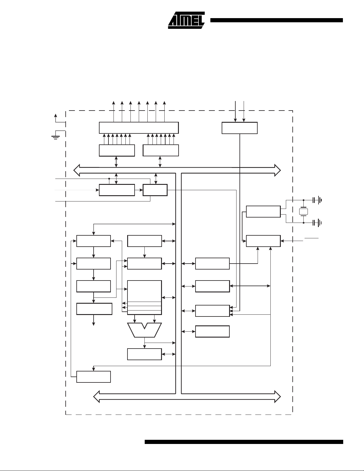
Block Diagram
Figure 1. The AT90C8534 Block Diagram
VCC
GND
AVCC
ADIN5..0
AGND
PROGRAM
COUNTER
PROGRAM
FLASH
PA0 - PA6
PORTA DRIVERS
DATA REGISTER
PORTA
ANALOG MUX ADC
REG. PORTA
STACK
POINTER
SRAM
DATA DIR.
8-BIT DATA BUS
MCU CONTROL
REGISTER
INT1,0
EXTERNAL
INTERRUPTS
OSCILLATOR
TIMING AND
CONTROL
XTAL1
XTAL2
RESET
INSTRUCTION
REGISTER
INSTRUCTION
DECODER
CONTROL
LINES
PROGRAMMING
LOGIC
2
AT90C8534
GENERAL
PURPOSE
REGISTERS
X
Y
Z
ALU
STATUS
REGISTER
TIMER/
COUNTERS
INTERRUPT
UNIT
EEPROM
Page 3

AT90C8534
The AVR core combines a rich instruction set with 32 general-purpose working registers. All the 32 registers are directly
connected to the Arithmetic Logic Unit (ALU), allowing two independent registers to be accessed in one single instruction
executed in one clock cycle. The resulting architecture is more code efficient while achieving throughputs up to ten times
faster than conventional CISC microcontrollers.
The AT90C8534 provides the following features: 8K bytes of programmable Flash, 512 bytes EEPROM, 256 bytes SRAM,
7 general output lines, 2 external interrupt lines, 32 general-purpose working registers, 2 flexible timer/counters, internal
and external interrupts, 6-channel, 10-bit ADC, and 2 software-selectable power saving modes. The Idle mode stops the
CPU while allowing the ADC, timer/counters and interrupt system to continue functioning. The Power-down mode saves
the SRAM and register contents but freezes the oscillator, disabling all other chip functions until the next interrupt or hardware reset.
The device is manufactured using Atmel’s high-density nonvolatile memory technology. The on-chip programmable Flash
allows the program memory to be reprogrammed by a conventional nonvolatile memory programmer. By combining an
8-bit RISC CPU with programmable Flash on a monolithic chip, the Atmel AT90C8534 is a powerful microcontroller that
provides a highly flexible and cost-effective solution to many embedded control applications.
The AT90C8534 AVR is supported with a full suite of program and system development tools including: C compilers, macro
assemblers, program debugger/simulators, in-circuit emulators and evaluation kits.
Pin Descriptions
VCC
Digital supply voltage
GND
Digital ground
Port A (PA6..PA0)
Port A is a 7-bit output port with tri-state mode. The Port A output buffers can sink 20 mA and can drive LED displays
directly. The port pins are tri-stated when a reset condition becomes active, even if the clock is not running.
INT1, 0
External interrupt input pins. A falling or rising edge on either of these pins will generate an interrupt request. Interrupt
pulses longer than 40 ns will generate an interrupt, even if the clock is not running.
ADIN5..0
ADC input pins. Any of these pins can be selected as the input to the ADC.
RESET
Reset input. An external reset is generated by a low level on the RESET pin. Reset pulses longer than 100 ns will generate
a reset, even if the clock is not running. Shorter pulses are not guaranteed to generate a reset.
XTAL1
Input to the inverting oscillator amplifier and input to the internal clock operating circuit.
XTAL2
Output from the inverting oscillator amplifier
AVCC
This is the supply voltage pin for the A/D Converter. If the ADC is not used, the pin must be connected to V
used, the pin should be connected to VCC via a low-pass filter. See page 30 for details on operation of the ADC.
AGND
Analog ground. If the board has a separate analog ground plane, this pin should be connected to this ground plane.
Otherwise, connect to GND.
. If the ADC is
CC
3
Page 4
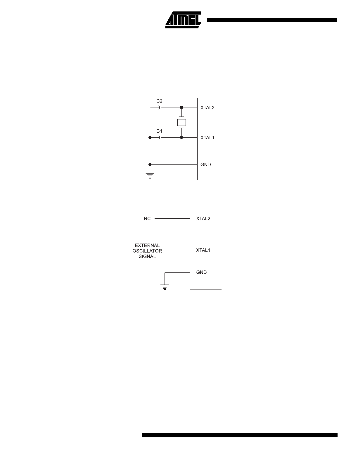
Crystal Oscillators
XTAL1 and XTAL2 are input and output, respectively, of an inverting amplifier that can be configured for use as an on-chip
oscillator, as shown in Figure 2. Either a quartz crystal or a ceramic resonator may be used. To drive the device from an
external clock source, XTAL2 should be left unconnected while XTAL1 is driven as shown in Figure 3. Note that XTAL2
should not be used to drive other components.
Figure 2. Oscillator Connections
Figure 3. External Clock Drive Configuration
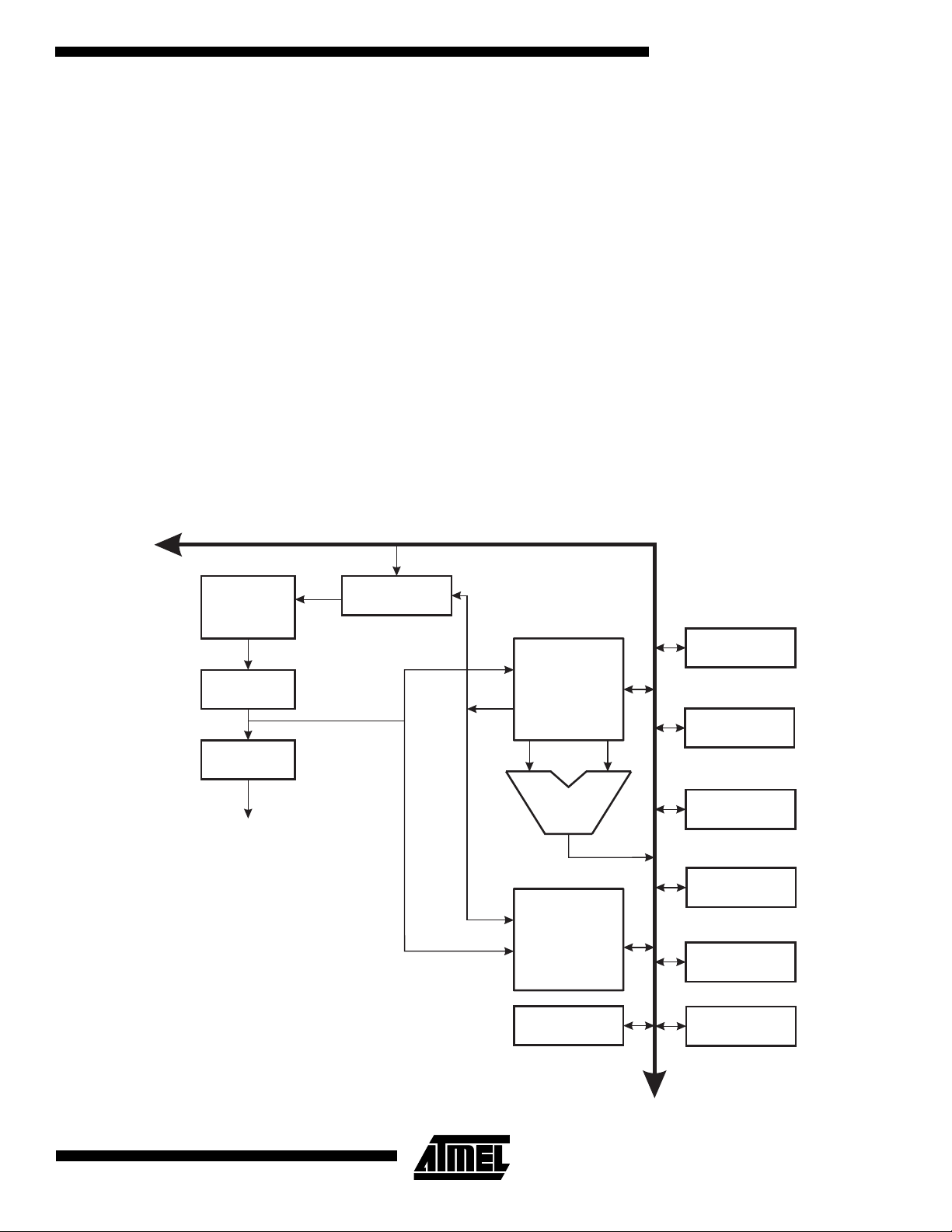
Architectural Overview
The fast-access register file concept contains 32 x 8-bit general-purpose working registers with a single clock cycle access
time. This means that during one single clock cycle, one ALU (Arithmetic Logic Unit) operation is executed. Two operands
are output from the register file, the operation is executed and the result is stored back in the register file – in one clock
cycle.
Six of the 32 registers can be used as three 16-bit indirect address register pointers for Data Space addressing, enabling
efficient address calculations. One of the three address pointers is also used as the address pointer for the constant table
look-up function. These added function registers are the 16-bit X-register, Y-register and Z-register.
The ALU supports arithmetic and logic functions between registers or between a constant and a register. Single register
operations are also executed in the ALU. Figure 4 shows the AT90C8534 AVR RISC microcontroller architecture.
In addition to the register operation, the conventional memory addressing modes can be used on the register file as well.
This is enabled by the fact that the register file is assigned the 32 lowermost Data Space addresses ($00 - $1F), allowing
them to be accessed as though they were ordinary memory locations.
4
AT90C8534
Page 5
AT90C8534
The I/O memory space contains 64 addresses for CPU peripheral functions such as Control Registers, Timer/Counters,
A/D converters and other I/O functions. The I/O memory can be accessed directly or as the Data Space locations
following those of the register file, $20 - $5F.
The AVR uses a Harvard architecture concept – with separate memories and buses for program and data. The program
memory is executed with a single-level pipelining. While one instruction is being executed, the next instruction is
pre-fetched from the program memory. This concept enables instructions to be executed in every clock cycle. The program
memory is programmable Flash memory.
With the relative jump and call instructions, the whole 4K word (8K bytes) address space is directly accessed. Most AVR
instructions have a single 16-bit word format. Every program memory address contains a 16- or 32-bit instruction.
During interrupts and subroutine calls, the return address program counter (PC) is stored on the stack. The stack is effectively allocated in the general data SRAM and, consequently, the stack size is only limited by the total SRAM size and the
usage of the SRAM. All user programs must initialize the stack pointer (SP) in the reset routine (before subroutines or
interrupts are executed). The 9-bit stack pointer is read/write accessible in the I/O space.
The 256 bytes data SRAM can be easily accessed through the five different addressing modes supported in the AVR
architecture.
The memory spaces in the AVR architecture are all linear and regular memory maps.
Figure 4. The AT90C8534 AVR RISC Architecture
AVR
4K X 16
Program
Memory
Instruction
Register
Instruction
Decoder
Control Lines
AT90C8534 Architecture
Program
Counter
32 x 8
General
Purpose
Registrers
Direct Addressing
Indirect Addressing
256 x 8
SRAM
Data Bus 8-bit
ALU
Data
Interrupt
Unit
Status
and Control
8-bit
Timer/Counter
16-bit
Timer/Counter
Analog to Digital
Converter
512 x 8
EEPROM
7
Output Lines
5
Page 6

Figure 5. Memory Maps
Data MemoryProgram Memory
Program Flash
(4K x 16)
$000
32 Gen. Purpose
Working Registers
64 I/O Registers
Internal SRAM
(256 x 8)
$0000
$001F
$0020
$005F
$0060
$015F
$FFF
A flexible interrupt module has its control registers in the I/O space with an additional global interrupt enable bit in the status
register. All the different interrupts have a separate interrupt vector in the interrupt vector table at the beginning of the
program memory. The different interrupts have priority in accordance with their interrupt vector position. The lower the
interrupt vector address, the higher the priority.
6
AT90C8534
Page 7
General-purpose Register File
Figure 6 shows the structure of the 32 general-purpose working registers in the CPU.
Figure 6. AVR CPU General-purpose Working Registers
70Addr.
R0 $00
R1 $01
R2 $02
…
R13 $0D
General R14 $0E
Purpose R15 $0F
Working R16 $10
Registers R17 $11
…
R26 $1A X-register low byte
R27 $1B X-register high byte
R28 $1C Y-register low byte
R29 $1D Y-register high byte
R30 $1E Z-register low byte
R31 $1F Z-register high byte
AT90C8534
All the register operating instructions in the instruction set have direct and single-cycle access to all registers. The only
exception are the five constant arithmetic and logic instructions SBCI, SUBI, CPI, ANDI and ORI between a constant and a
register and the LDI instruction for load immediate constant data. These instructions apply to the second half of the
registers in the register file – R16..R31. The general SBC, SUB, CP, AND and OR and all other operations between two
registers or on a single register apply to the entire register file.
As shown in Figure 6, each register is also assigned a data memory address, mapping them directly into the first 32 locations of the user Data Space. Although not being physically implemented as SRAM locations, this memory organization
provides great flexibility in access of the registers, as the X-, Y- and Z-registers can be set to index any register in the file.
X-register, Y-register and Z-register
The registers R26..R31 have some added functions to their general-purpose usage. These registers are address pointers
for indirect addressing of the Data Space. The three indirect address registers X, Y and Z are defined as:
Figure 7. X-, Y- and Z-registers
15 0
X-register 7 0 7 0
R27 ($1B) R26 ($1A)
15 0
Y-register 7 0 7 0
R29 ($1D) R28 ($1C)
15 0
Z-register 7 0 7 0
R31 ($1F) R30 ($1E)
In the different addressing modes these address registers have functions as fixed displacement, automatic increment and
decrement (see the descriptions for the different instructions).
7
Page 8
ALU – Arithmetic Logic Unit
The high-performance AVR ALU operates in direct connection with all the 32 general-purpose working registers. Within a
single clock cycle, ALU operations between registers in the register file are executed. The ALU operations are divided into
three main categories: arithmetic, logical and bit functions.
Programmable Flash Program Memory
The AT90C8534 contains 8K bytes of on-chip programmable Flash memory for program storage. Since all instructions are
16- or 32-bit words, the Flash is organized as 4K x 16. The Flash memory has an endurance of at least 1000 write/erase
cycles. The AT90C8534 program counter (PC) is 12 bits wide, thus addressing the 4096 program memory addresses.
Constant tables must be allocated within the address 0 - 4K (see the LPM – Load Program Memory instruction description).
See page 9 for the different program memory addressing modes.
SRAM Data Memory
The following figure shows how the AT90C8534 SRAM memory is organized.
Figure 8. SRAM Organization
Register File
R0
R1
R2
...
R29
R30
R31
I/O Registers
$00
$01
$02
...
$3D
$3E
$3F
Data Address Space
$0000
$0001
$0002
...
$001D
$001E
$001F
$0020
$0021
$0022
...
$005D
$005E
$005F
Internal SRAM
$0060
$0061
...
$015E
$015F
The lower 352 data memory locations address the register file, the I/O memory and the internal data SRAM. The first
96 locations address the register file + I/O memory, and the next 256 locations address the internal data SRAM.
The five different addressing modes for the data memory cover: Direct, Indirect with Displacement, Indirect, Indirect with
Pre-decrement and Indirect with Post-increment. In the register file, registers R26 to R31 feature the indirect addressing
pointer registers.
The direct addressing reaches the entire data space.
8
AT90C8534
Page 9
AT90C8534
The Indirect with Displacement mode features 63 address locations reached from the base address given by the Y- or
Z-register.
When using register indirect addressing modes with automatic pre-decrement and post-increment, the address registers X,
Y and Z are decremented and incremented.
The 32 general-purpose working registers, 64 I/O registers and the 256 bytes of internal data SRAM in the AT90C8534 are
all accessible through all these addressing modes.
See the next section for a detailed description of the different addressing modes.
Program and Data Addressing Modes
The AT90C8534 AVR RISC microcontroller supports powerful and efficient addressing modes for access to the program
memory (Flash) and data memory (SRAM, Register file and I/O memory). This section describes the different addressing
modes supported by the AVR architecture. In the figures, OP means the operation code part of the instruction word. To
simplify, not all figures show the exact location of the addressing bits.
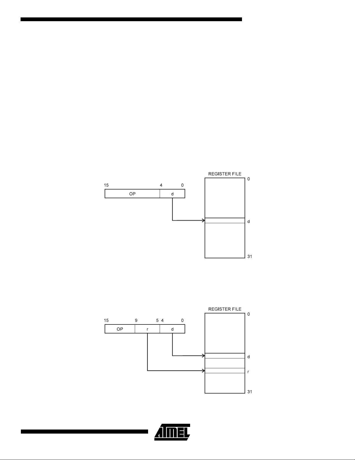
Register Direct, Single Register Rd
Figure 9. Direct Single Register Addressing
The operand is contained in register d (Rd).
Register Direct, Two Registers Rd And Rr
Figure 10. Direct Register Addressing, Two Registers
Operands are contained in register r (Rr) and d (Rd). The result is stored in register d (Rd).
9
Page 10

I/O Direct
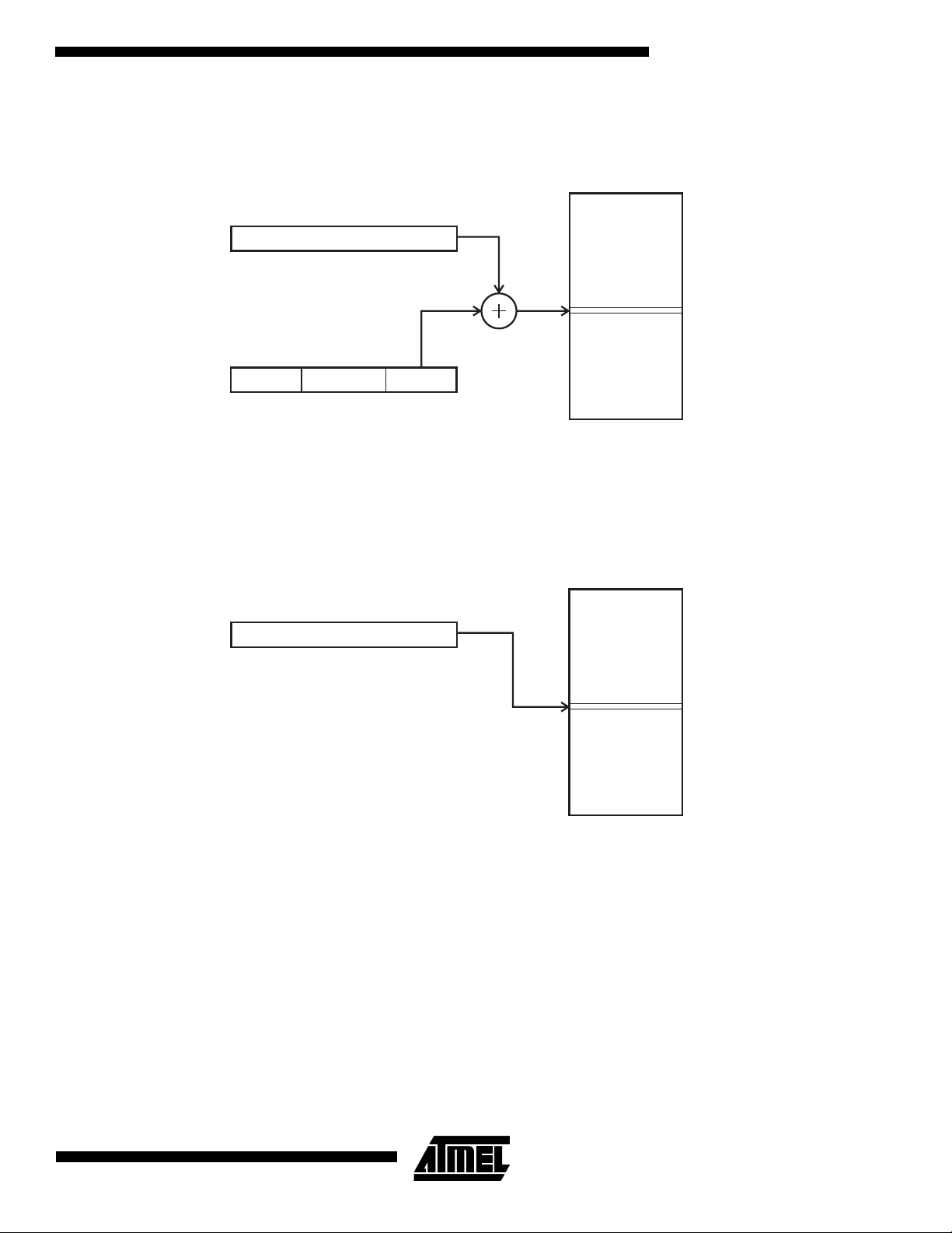
Figure 11. I/O Direct Addressing
Operand address is contained in six bits of the instruction word. n is the destination or source register address.
Data Direct
Figure 12. Direct Data Addressing
Data Space
31
OP Rr/Rd
15 0
20 19
16 LSBs
16
$0000
$015F
A 16-bit data address is contained in the 16 LSBs of a 2-word instruction. Rd/Rr specify the destination or source register.
10
AT90C8534
Page 11
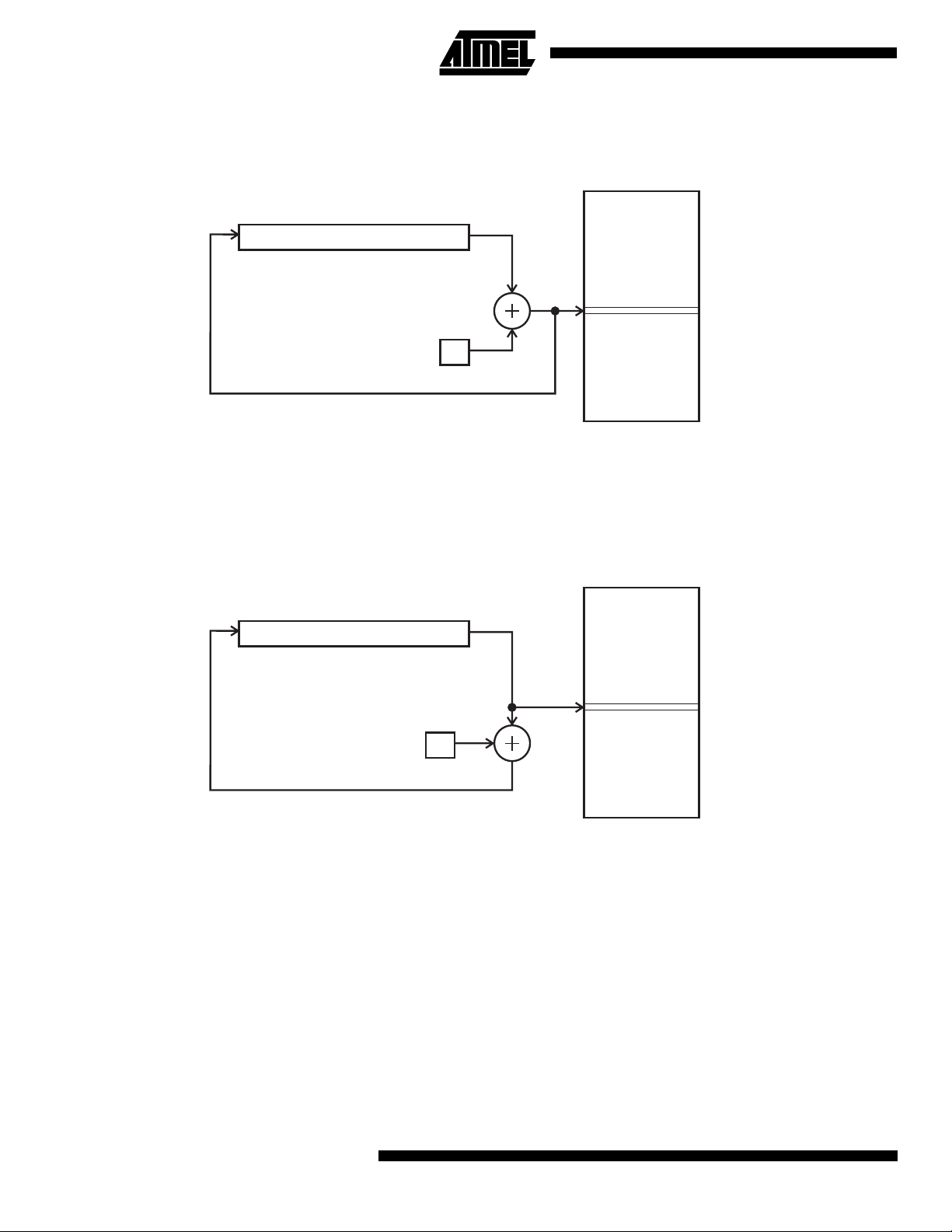
Data Indirect with Displacement
Figure 13. Data Indirect with Displacement
AT90C8534
15
Y OR Z - REGISTER
15
OP an
Data Space
0
05610
$0000
$015F
Operand address is the result of the Y- or Z-register contents added to the address contained in six bits of the instruction
word.
Data Indirect
Figure 14. Data Indirect Addressing
Data Space
015
X, Y OR Z - REGISTER
$0000
Operand address is the contents of the X-, Y- or the Z-register.
$015F
11
Page 12
Data Indirect with Pre-decrement
Figure 15. Data Indirect Addressing with Pre-decrement
Data Space
015
X, Y OR Z - REGISTER
-1
$0000
$015F
The X-, Y- or the Z-register is decremented before the operation. Operand address is the decremented contents of the X-,
Y- or the Z-register.
Data Indirect with Post-increment
Figure 16. Data Indirect Addressing with Post-increment
Data Space
015
X, Y OR Z - REGISTER
$0000
1
$015F
The X-, Y- or the Z-register is incremented after the operation. Operand address is the content of the X-, Y- or the Z-register
prior to incrementing.
12
AT90C8534
Page 13
AT90C8534
Constant Addressing Using the LPM Instruction
Figure 17. Code Memory Constant Addressing
Constant byte address is specified by the Z-register contents. The 15 MSBs select word address (0 - 4K), the LSB selects
low byte if cleared (LSB = 0) or high byte if set (LSB = 1).
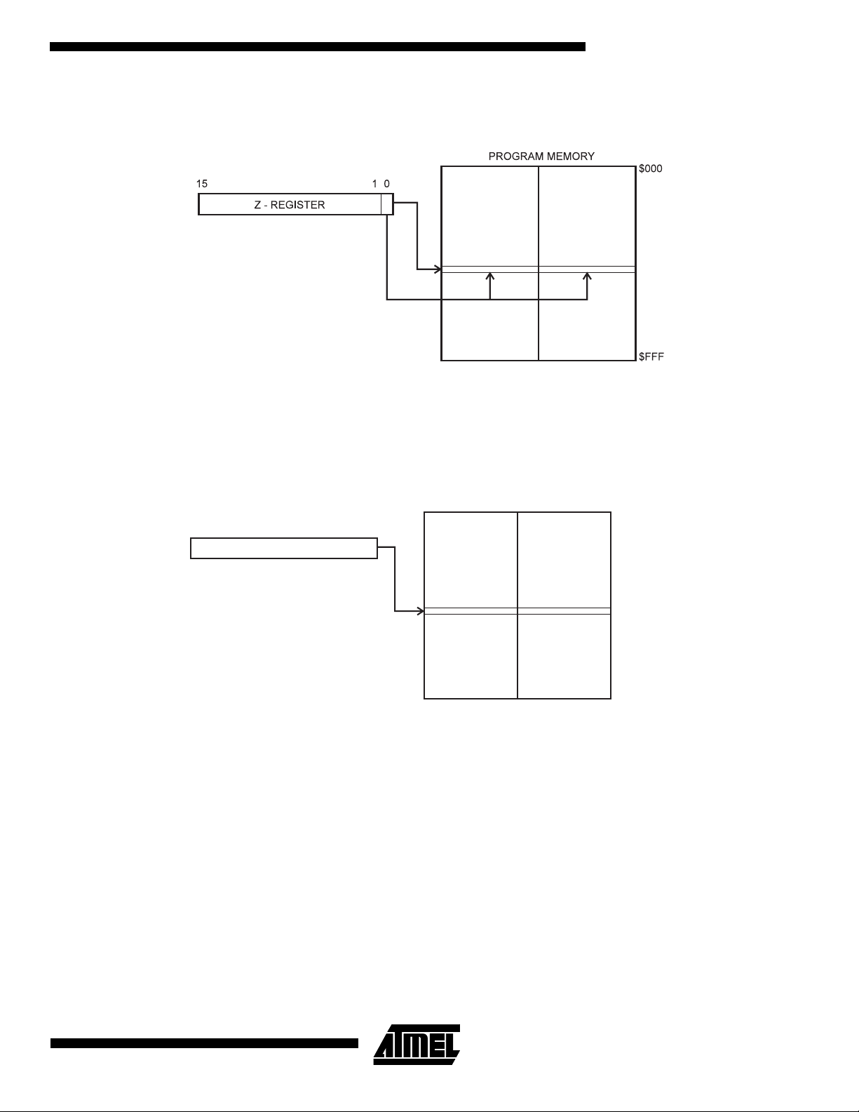
Indirect Program Addressing, IJMP and ICALL
Figure 18. Indirect Program Memory Addressing
PROGRAM MEMORY
$000
15 0
Z-REGISTER
$7FF/$FFF
Program execution continues at address contained by the Z-register (i.e., the PC is loaded with the contents of the
Z-register).
13
Page 14
Relative Program Addressing, RJMP And RCALL
Figure 19. Relative Program Memory Addressing
+1
Program execution continues at address PC + k + 1. The relative address k is from -2048 to 2047.
EEPROM Data Memory
The AT90C8534 contains 512 bytes of data EEPROM memory. It is organized as a separate data space, in which single
bytes can be read and written. The EEPROM has an endurance of at least 100,000 write/erase cycles. The access
between the EEPROM and the CPU is described on page 28, specifying the EEPROM Address Registers, the EEPROM
Data Register, and the EEPROM Control Register.
Memory Access Times and Instruction Execution Timing
This section describes the general access timing concepts for instruction execution and internal memory access.
The AVR CPU is driven by the System Clock Ø, directly generated from the external clock crystal for the chip. No internal
clock division is used.
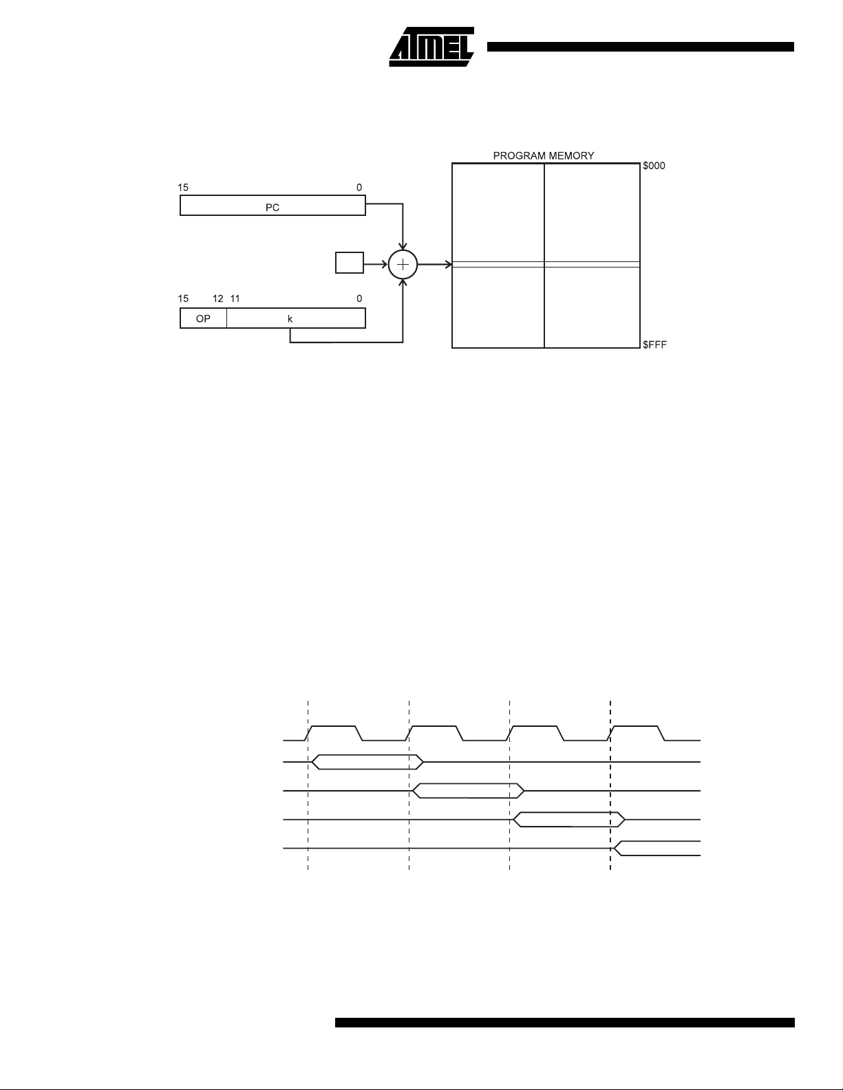
Figure 20 shows the parallel instruction fetches and instruction executions enabled by the Harvard architecture and the
fast-access register file concept. This is the basic pipelining concept to obtain up to 1 MIPS per MHz with the corresponding
unique results for functions per cost, functions per clocks and functions per power unit.
Figure 20. The Parallel Instruction Fetches and Instruction Executions
T1 T2 T3 T4
System Clock Ø
1st Instruction Fetch
1st Instruction Execute
2nd Instruction Fetch
2nd Instruction Execute
3rd Instruction Fetch
3rd Instruction Execute
4th Instruction Fetch
14
AT90C8534
Page 15
AT90C8534
Figure 21 shows the internal timing concept for the register file. In a single clock cycle an ALU operation using two register
operands is executed and the result is stored back to the destination register.
Figure 21. Single Cycle ALU Operation
T1 T2 T3 T4
System Clock Ø
Total Execution Time
Register Operands Fetch
ALU Operation Execute
Result Write Back
The internal data SRAM access is performed in two System Clock cycles as described in Figure 22.
Figure 22. On-Chip Data SRAM Access Cycles
T1 T2 T3 T4
System Clock Ø
Address
Data
WR
Data
RD
Prev. Address
Address
Write
Read
15
Page 16

I/O Memory
The I/O space definition of the AT90C8534 is shown in Table 1.
Table 1. AT90C8534 I/O Space
I/O Address (SRAM Address) Name Function
$3F ($5F) SREG Status REGister
$3E ($5E) SPH Stack Pointer High
$3D ($5D) SPL Stack Pointer Low
$3B ($5B) GIMSK General Interrupt MaSK register
$3A ($5A) GIFR General Interrupt Flag Register
$39 ($59) TIMSK Timer/Counter Interrupt MaSK register
$38 ($58) TIFR Timer/Counter Interrupt Flag register
$35 ($55) MCUCR MCU general Control Register
$33 ($53) TCCR0 Timer/Counter0 Control Register
$32 ($52) TCNT0 Timer/Counter0 (8-bit)
$2E ($4E) TCCR1 Timer/Counter1 Control Register
$2D ($4D) TCNT1H Timer/Counter1 High Byte
$2C ($4C) TCNT1L Timer/Counter1 Low Byte
$1F ($3E) EEARH EEPROM Address Register High Byte
$1E ($3E) EEARL EEPROM Address Register Low Byte
$1D ($3D) EEDR EEPROM Data Register
$1C ($3C) EECR EEPROM Control Register
$1B ($3B) PORTA Data Register, Port A
$1A ($3A) DDRA Data Direction Register, Port A
$10 ($30) GIPR General Interrupt Pin Register
$07 ($27) ADMUX ADC Multiplexer Select Register
$06 ($26) ADCSR ADC Control and Status Register
$05 ($25) ADCH ADC Data Register High
$04 ($24) ADCL ADC Data Register Low
Note: Reserved and unused locations are not shown in the table.
The AT90C8534 I/Os and peripherals are placed in the I/O space. The I/O locations are accessed by the IN and OUT
instructions transferring data between the 32 general-purpose working registers and the I/O space. I/O registers within the
address range $00 - $1F are directly bit-accessible using the SBI and CBI instructions. In these registers, the value of
single bits can be checked by using the SBIS and SBIC instructions. Refer to the instruction set section for more details.
When using the I/O specific commands, IN and OUT, the I/O addresses $00 - $3F must be used. When addressing I/O registers as SRAM, $20 must be added to this address. All I/O register addresses throughout this document are shown with
the SRAM address in parentheses.
For compatibility with future devices, reserved bits should be written to zero if accessed. Reserved I/O memory addresses
should never be written.
The I/O and peripherals control registers are explained in the following sections.
16
AT90C8534
Page 17

AT90C8534
Status Register – SREG
The AVR status register (SREG) at I/O space location $3F ($5F) is defined as:
Bit 76543210
$3F ($5F) I T H S V N Z C SREG
Read/Write R/W R/W R/W R/W R/W R/W R/W R/W
Initial value 0 0 0 0 0 0 0 0
Bit 7 – I: Global Interrupt Enable
•
The global interrupt enable bit must be set (one) for the interrupts to be enabled. The individual interrupt enable control is
then performed in separate control registers. If the global interrupt enable bit is cleared (zero), none of the interrupts are
enabled independent of the individual interrupt enable settings. The I-bit is cleared by hardware when an interrupt routine is
entered and is set by the RETI instruction to enable subsequent interrupts.
Bit 6 – T: Bit Copy Storage
•
The bit copy instructions BLD (Bit LoaD) and BST (Bit STore) use the T-bit as source and destination for the operated bit. A
bit from a register in the register file can be copied into T by the BST instruction and a bit in T can be copied into a bit in a
register in the register file by the BLD instruction.
Bit 5 – H: Half-carry Flag
•
The half-carry flag H indicates a half-carry in some arithmetical operations. See the Instruction Set description for detailed
information.
Bit 4 – S: Sign Bit, S = N⊄⊕ V
•
The S-bit is always an exclusive or between the negative flag N and the two’s complement overflow flag V. See the Instruction Set description for detailed information.
•
Bit 3 – V: Two’s Complement Overflow Flag
The two’s complement overflow flag V supports two’s complement arithmetics. See the Instruction Set description for
detailed information.
Bit 2 – N: Negative Flag
•
The negative flag N indicates a negative result from an arithmetical or logical operations. See the Instruction Set description for detailed information.
Bit 1 – Z: Zero Flag
•
The zero flag Z indicates a zero result from an arithmetical or logical operations. See the Instruction Set description for
detailed information.
•
Bit 0 – C: Carry Flag
The carry flag C indicates a carry in an arithmetical or logic operation. See the Instruction Set description for detailed
information.
Note that the status register is not automatically stored when entering an interrupt routine or restored when returning from
an interrupt routine. This must be handled by software.
Stack Pointer – SP
The AT90C8534 Stack Pointer is implemented as two 8-bit registers in the I/O space locations $3E ($5E) and $3D ($5D).
As the AT90C8534 data memory has $15F locations, nine bits are used.
Bit 151413121110 9 8
$3E ($5E) –––––––SP8 SPH
$3D ($5D) SP7 SP6 SP5 SP4 SP3 SP2 SP1 SP0 SPL
76543210
Read/Write RRRRRRRR/W
R/W R/W R/W R/W R/W R/W R/W R/W
Initial value 0 0 0 0 0 0 0 0
00000000
The Stack Pointer points to the data SRAM stack area where the Subroutine and Interrupt Stacks are located. This stack
space in the data SRAM must be defined by the program before any subroutine calls are executed or interrupts are
enabled. The Stack Pointer is decremented by 1 when data is pushed onto the stack with the PUSH instruction and it is
17
Page 18

decremented by 2 when data is pushed onto the stack with subroutine RCALL and interrupt. The Stack Pointer is incremented by 1 when data is popped from the stack with the POP instruction and it is incremented by 2 when data is popped
from the stack with return from subroutine RET or return from interrupt RETI.
Reset and Interrupt Handling
The AT90C8534 provides six different interrupt sources. These interrupts and the separate reset vector each have a
separate program vector in the program memory space. All interrupts are assigned individual enable bits that must be set
(one) together with the I-bit in the status register in order to enable the interrupt.
The lowest addresses in the program memory space are automatically defined as the Reset and Interrupt vectors. The
complete list of vectors is shown in Table 2. The list also determines the priority levels of the different interrupts. The lower
the address, the higher the priority level. RESET has the highest priority and next is INT0 (the External Interrupt Request
0), etc.
Table 2. Reset and Interrupt Vectors
Vector No. Program Address Source Interrupt Definition
1 $000 RESET Hardware Pin
2 $001 INT0 External Interrupt Request 0
3 $002 INT1 External Interrupt Request 1
4 $003 TIMER1 OVF Timer/Counter1 Overflow
5 $004 TIMER0 OVF Timer/Counter0 Overflow
6 $005 ADC ADC Conversion Complete
7 $006 EE_RDY EEPROM Ready
The most typical program setup for the Reset and Interrupt vector addresses are:
Address Labels Code Comments
$000 rjmp RESET ; Reset Handler
$001 rjmp EXT_INT0 ; IRQ0 Handler
$002 rjmp EXT_INT1 ; IRQ1 Handler
$003 rjmp TIM1_OVF ; Timer1 Overflow Handler
$004 rjmp TIM0_OVF ; Timer0 Overflow Handler
$005 rjmp ADC ; ADC Conversion Complete Interrupt Handler
$006 rjmp EE_RDY ; EEPROM Ready Handler
;
$007 MAIN: ldi r16, high(RAMEND); Main program start
out SPH, r16
ldi r16, low(RAMEND)
out SPL, r16
<instr> xxx
…………
18
AT90C8534
Page 19

AT90C8534
Reset
During reset, all I/O registers are set to their initial values and the program counter is set to address $000. When reset is
released, the program starts execution from this address. The instruction placed in address $000 must be an RJMP (relative jump) instruction to the reset handling routine. If the program never enables an interrupt source, the interrupt vectors
are not used and regular program code can be placed at these locations. The circuit diagram in Figure 23 shows the reset
logic. Table 3 defines the timing and electrical parameters of the reset circuitry
Figure 23. Reset Logic
CLOCK
Table 3. Reset Characteristics (V
Symbol Parameter Min Typ Max Units
V
RST
t
TOUT
RESET Pin Threshold Voltage 0.6 V
Reset Delay Time-out Period - 1026 - clocks
= 5.0V)
CC
CC
V
External reset
The AT90C8534 has one source of reset: the external reset pin. The external reset is used for three purposes:
1. Power-on Reset. During power-on, the external reset must be held active (low) until 100 ns after V
has reached
CC
the minimum operation voltage.
2. Brown-out Reset. If V
active immediately, and must be held active until 100 ns after V
drops below the minimum operation voltage during operation, the external reset must go
CC
rises to the minimum operation voltage.
CC
3. Normal Operation Reset. During normal operation, reset is generated by holding the external reset active for at
least 100 ns.
When the external reset is released, an internal timer that is clocked from the external clock input is started, holding the
internal reset active until the external clock source has toggled a certain number of times (see Table 3). This is illustrated in
Figure 24 and Figure 25.
19
Page 20

Figure 24. External Reset on Start-up
V
VCC
RESET
TIME-OUT
INTERNAL
RESET
POT
Figure 25. External Reset during Operation
V
RST
t
TOUT
Interrupt Handling
The AT90C8534 has two 8-bit Interrupt Mask control registers; GIMSK (General Interrupt Mask register) and TIMSK
(Timer/Counter Interrupt Mask register).
When an interrupt occurs, the Global Interrupt Enable I-bit is cleared (zero) and all interrupts are disabled. The user software can set (one) the I-bit to enable nested interrupts. The I-bit is set (one) when a Return from Interrupt instruction (RETI)
is executed.
When the Program Counter is vectored to the actual interrupt vector in order to execute the interrupt handling routine, hardware clears the corresponding flag that generated the interrupt. Some of the interrupt flags can also be cleared by writing a
logical “1” to the flag bit position(s) to be cleared.
If an interrupt condition occurs when the corresponding interrupt enable bit is cleared (zero), the interrupt flag will be set
and remembered until the interrupt is enabled or the flag is cleared by software.
If one or more interrupt conditions occur when the global interrupt enable bit is cleared (zero), the corresponding interrupt
flag(s) will be set and remembered until the global interrupt enable bit is set (one), and will be executed by order of priority.
Note that the status register is not automatically stored when entering an interrupt routine and restored when returning from
an interrupt routine. This must be handled by software.
20
AT90C8534
Page 21

AT90C8534
General Interrupt Mask Register – GIMSK
Bit 76543210
$3B ($5B) INT1 INT0 ––––––GIMSK
Read/Write R/W R/W R R R R R R
Initial value 00000000
Bit 7 – INT1: External Interrupt Request 1 Enable
•
When the INT1 bit is set (one) and the I-bit in the Status Register (SREG) is set (one), the external pin interrupt is enabled.
The external interrupt is activated on falling or rising edge of the INT1 pin. The corresponding interrupt of External Interrupt
Request 1 is executed from program memory address $002. See also “External Interrupts”.
Bit 6 – INT0: External Interrupt Request 0 Enable
•
When the INT0 bit is set (one) and the I-bit in the Status Register (SREG) is set (one), the external pin interrupt is enabled.
The external interrupt is activated on falling or rising edge of the INT0 pin. The corresponding interrupt of External Interrupt
Request 0 is executed from program memory address $001. See also “External Interrupts”.
Bits 5..0 – Res: Reserved Bits
•
These bits are reserved bits in the AT90C8534 and always read as zero.
General Interrupt Flag Register – GIFR
Bit 76543 210
$3A ($5A) INTF1 INTF0 ––––––GIFR
Read/Write R/W R/W R R R R R R
Initial value 00000000
Bit 7 – INTF1: External Interrupt Flag 1
•
When an event on the INT1 pin triggers an interrupt request, INTF1 becomes set (one). If the I-bit in SREG and the INT1 bit
in GIMSK are set (one), the MCU will jump to the interrupt vector at address $002. The flag is cleared when fetching the
interrupt vector. Alternatively, the flag can be cleared by writing a logical “1” to it.
Bit 6 – INTF0: External Interrupt Flag 0
•
When an event on the INT0 pin triggers an interrupt request, INTF0 becomes set (one). If the I-bit in SREG and the INT0 bit
in GIMSK are set (one), the MCU will jump to the interrupt vector at address $001. The flag is cleared when fetching the
interrupt vector. Alternatively, the flag can be cleared by writing a logical “1” to it.
Bits 5..0 – Res: Reserved Bits
•
These bits are reserved bits in the AT90C8534 and always read as zero.
General Interrupt Pin Register – GIPR
Bit 76543210
$10 ($30) ––––IPIN1 IPIN0 ––GIPR
Read/Write RRRRRRRR
Initial value 0 0 0 0 x x 0 0
Bits 7..4 – Res: Reserved Bits
•
These bits are reserved bits in the AT90C8534 and always read as zero.
•
Bit 3 – IPIN1: External Interrupt Pin 1
Reading this bit returns the logical value present on input pin INT1 (after synchronization latches).
Bit 2 – IPIN0: External Interrupt Pin 0
•
Reading this bit returns the logical value present on input pin INT0 (after synchronization latches).
Bits 1..0 – Res: Reserved Bits
•
These bits are reserved bits in the AT90C8534 and always read as zero.
21
Page 22

Timer/Counter Interrupt Mask Register – TIMSK
Bit 76543210
$39 ($59) –––––TOIE1 – TOIE0 TIMSK
Read/Write RRRRRR/WRR/W
Initial value 00000000
Bits 7..3 – Res: Reserved Bits
•
These bits are reserved bits in the AT90C8534 and always read as zero.
•
Bit 2 – TOIE1: Timer/Counter1 Overflow Interrupt Enable
When the TOIE1 bit is set (one) and the I-bit in the Status Register is set (one), the Timer/Counter1 Overflow interrupt is
enabled. The corresponding interrupt (at vector $003) is executed if an overflow in Timer/Counter1 occurs, i.e., when the
Overflow Flag (Timer/Counter1) is set (one) in the Timer/Counter Interrupt Flag Register (TIFR).
Bit 1 – Res: Reserved Bit
•
This bit is a reserved bit in the AT90C8534 and always reads as zero.
•
Bit 0 – TOIE0: Timer/Counter0 Overflow Interrupt Enable
When the TOIE0 bit is set (one) and the I-bit in the Status Register is set (one), the Timer/Counter0 Overflow interrupt is
enabled. The corresponding interrupt (at vector $004) is executed if an overflow in Timer/Counter0 occurs, i.e., when the
Overflow Flag (Timer0) is set (one) in the Timer/Counter Interrupt Flag Register (TIFR).
Timer/Counter Interrupt Flag Register – TIFR
Bit 76543210
$38 ($58) –––––TOV1 – TOV0 TIFR
Read/Write RRRRRR/WRR/W
Initial value 00000000
Bits 7..3 – Res: Reserved Bits
•
These bits are reserved bits in the AT90C8534 and always read as zero.
Bit 2 – TOV1: Timer/Counter1 Overflow Flag
•
The TOV1 is set (one) when an overflow occurs in Timer/Counter1. TOV1 is cleared when fetching the interrupt vector.
Alternatively, TOV1 is cleared by writing a logical “1” to the flag. When the I-bit in SREG and TOIE1 (Timer/Counter1
Overflow Interrupt Enable) and TOV1 are set (one), the Timer/Counter1 Overflow Interrupt is executed.
Bit 1 – Res: Reserved Bit
•
This bit is a reserved bit in the AT90C8534 and always reads as zero.
•
Bit 0 – TOV0: Timer/Counter0 Overflow Flag
The bit TOV0 is set (one) when an overflow occurs in Timer/Counter0. TOV0 is cleared when fetching the interrupt vector.
Alternatively, TOV0 is cleared by writing a logical “1” to the flag. When the SREG I-bit and TOIE0 (Timer/Counter0 Overflow Interrupt Enable) and TOV0 are set (one), the Timer/Counter0 Overflow interrupt is executed.
External Interrupts
The external interrupts are triggered by the INT1 and INT0 pins. The external interrupts can be triggered by a falling or
rising edge.
Interrupt Response Time
The interrupt execution response for all the enabled AVR interrupts is four clock cycles minimum. Four clock cycles after
the interrupt flag has been set, the program vector address for the actual interrupt handling routine is executed. During this
4-clock-cycle period, the Program Counter (2 bytes) is pushed onto the stack and the Stack Pointer is decremented by 2.
The vector is normally a relative jump to the interrupt routine, and this jump takes two clock cycles. If an interrupt occurs
during execution of a multi-cycle instruction, this instruction is completed before the interrupt is served.
A return from an interrupt handling routine (same as for a subroutine call routine) takes four clock cycles. During these four
clock cycles, the Program Counter (2 bytes) is popped back from the stack, the Stack Pointer is incremented by 2 and the
I-flag in SREG is set. When the AVR exits from an interrupt, it will always return to the main program and execute one more
instruction before any pending interrupt is served.
22
AT90C8534
Page 23

AT90C8534
MCU Control Register – MCUCR
The MCU Control Register contains control bits for general MCU functions.
Bit 76543210
$35 ($55) – SE SM ––ISC1 – ISC0 MCUCR
Read/Write R R/W R/W R R R/W R R/W
Initial value 0 0 0 0 0 0 0 0
Bit 7 – Res: Reserved Bit
•
This bit is reserved bits in the AT90C8534 and always reads as zero.
•
Bit 6 – SE: Sleep Enable
The SE bit must be set (one) to make the MCU enter the sleep mode when the SLEEP instruction is executed. To avoid the
MCU entering the sleep mode, unless it is the programmer’s purpose, it is recommended to set the Sleep Enable (SE) bit
just before the execution of the SLEEP instruction.
Bit 5 – SM: Sleep Mode
•
This bit selects between the two available sleep modes. When SM is cleared (zero), Idle Mode is selected as Sleep Mode.
When SM is set (one), Power-down Mode is selected as Sleep Mode. For details, refer to the section “Sleep Modes”.
Bit 4..3 – Res: Reserved Bits
•
These bits are reserved bits in the AT90C8534 and always read as zero.
•
Bit 2 – ISC1: Interrupt Sense Control 1
The external interrupt 1 is activated by the external pin INT1 if the SREG I-flag and the corresponding interrupt mask in the
GIMSK are set. If ISC1 is cleared (zero) a falling edge on INT1 activates the interrupt. If ISC1 is set (one), a rising edge on
INT1 activates the interrupt. Edges on INT2 are registered asynchronously. Pulses on INT1 wider than 40 ns will generate
an interrupt. Shorter pulses are not guaranteed to generate an interrupt.
When changing the ISC1 bit, an interrupt can occur. Therefore, it is recommended to first disable INT1 by clearing its interrupt Enable bit in the GIMSK register. Then ISC1 bit can be changed. Finally, the INT1 interrupt flag should be cleared by
writing a logical “1” to its interrupt Flag bit in the GIFR register before the interrupt is re-enabled.
Bit 1 – Res: Reserved Bit
•
This bit is reserved bits in the AT90C8534 and always reads as zero.
Bit 0 – ISC0: Interrupt Sense Control 0
•
The external interrupt 0 is activated by the external pin INT0 if the SREG I-flag and the corresponding interrupt mask in the
GIMSK are set. If ISC0 is cleared (zero), a falling edge on INT0 activates the interrupt. If ISC0 is set (one), a rising edge on
INT0 activates the interrupt. Pulses on INT0 wider than 40 ns will generate an interrupt. Shorter pulses are not guaranteed
to generate an interrupt.
When changing the ISC0 bit, an interrupt can occur. Therefore, it is recommended to first disable INT0 by clearing its interrupt Enable bit in the GIMSK register. Then ISC0 bit can be changed. Finally, the INT0 interrupt flag should be cleared by
writing a logical “1” to its interrupt Flag bit in the GIFR register before the interrupt is re-enabled.
Sleep Modes
To enter any of the two sleep modes, the SE bit in MCUCR must be set (one) and a SLEEP instruction must be executed.
The SM bit in the MCUCR register selects which sleep mode, Idle or Power-down, is activated by the SLEEP instruction.
If an enabled interrupt occurs while the MCU is in a sleep mode, the MCU awakes. The CPU is then halted for four cycles,
executes the interrupt routine and resumes execution from the instruction following SLEEP. The contents of the register
file, SRAM and I/O memory are unaltered. If a reset occurs during sleep mode, the MCU wakes up and executes from the
Reset vector.
Idle Mode
When the SM bit is cleared (zero), the SLEEP instruction forces the MCU into the Idle Mode, stopping the CPU but allowing
Timer/Counters, ADC and the interrupt system to continue operating. This enables the MCU to wake up from external
triggered interrupts as well as internal ones like the Timer Overflow and ADC interrupts.
23
Page 24

Power-down Mode
When the SM bit is set (one), the SLEEP instruction makes the MCU enter the Power-down Mode. In this mode, the
external oscillator is stopped, while the external interrupts continue operating. Only an external reset or an external edge
interrupt on INT0 or INT1 can wake up the MCU.
Note that if INT0 or INT1 is used for wake-up from Power-down Mode, the edge is remembered until the MCU wakes up.
When waking up from Power-down Mode, a delay from the wake-up condition occurs until the wake-up becomes effective.
This allows the clock to restart and become stable after having been stopped. The wake-up period is equal to the reset
delay time-out period t
TOUT
.
Timer/Counters
The AT90C8534 provides two general-purpose Timer/Counters – one 8-bit T/C and one 16-bit T/C. Timer/Counters 0 and
1 have individual prescaling selection from the same 10-bit prescaling timer.
Timer/Counter Prescaler
Figure 26. Prescaler for Timer/Counter0 and 1
For Timer/Counters 0 and 1, the five different prescaled selections are: CK, CK/8, CK/64, CK/256 and CK/1024, where CK
is the oscillator clock. In addition, the Timer/Counters can be stopped.
8-bit Timer/Counter0
Figure 27 shows the block diagram for Timer/Counter0.
The 8-bit Timer/Counter0 can select clock source from CK or prescaled CK. In addition, it can be stopped as described in
the specification for the Timer/Counter0 Control Register – TCCR0. The overflow status flag is found in the Timer/Counter
Interrupt Flag Register – TIFR. Control signals are found in the Timer/Counter0 Control Register – TCCR0. The interrupt
enable/disable setting for Timer/Counter0 is found in the Timer/Counter Interrupt Mask Register – TIMSK.
The 8-bit Timer/Counter0 features both a high resolution and a high accuracy usage with the lower prescaling opportunities. Similarly, the high prescaling opportunities make the Timer/Counter0 useful for lower speed functions or exact timing
functions with infrequent actions.
24
AT90C8534
Page 25

Figure 27. Timer/Counter0 Block Diagram
TA BUS
TIMER INT. MASK
REGISTER (TIMSK)
TOIE1
TOIE0
T/C0 OVER-
FLOW IRQ
TIMER INT. FLAG
REGISTER (TIFR)
AT90C8534
T/C0 CONTROL
REGISTER (TCCR0)
8-BIT DA
TIMER/COUNTER0
(TCNT0)
TOV0
TOV1
07
T/C CLK SOURCE
CONTROL
LOGIC
CS02
Timer/Counter0 Control Register – TCCR0
Bit 7 6 5 4 3 2 1 0
$33 ($53) –– – – –CS02 CS01 CS00 TCCR0
Read/Write R R R R R R/W R/W R/W
Initial value 0 0 0 0 0 0 0 0
Bits 7..3 – Res: Reserved Bits
•
These bits are reserved bits in the AT90C8534 and always read zero.
•
Bits 2, 1, 0 – CS02, CS01, CS00: Clock Select0, Bits 2, 1 and 0
The Clock Select0 bits 2, 1 and 0 define the prescaling source of Timer/Counter0.
Table 4. Clock 0 Prescale Select
CS02 CS01 CS00 Description
0 0 0 Stop, Timer/Counter0 is stopped.
CS01
CS00
CK
00 1CK
01 0CK/8
01 1CK/64
10 0CK/256
1 0 1 CK/1024
1 1 0 Reserved
1 1 1 Reserved
The Stop condition provides a Timer Enable/Disable function. The prescaled CK modes are scaled directly from the CK
oscillator clock.
25
Page 26

Timer Counter0 – TCNT0
Bit 76543210
$32 ($52) MSB LSB TCNT0
Read/Write R/W R/W R/W R/W R/W R/W R/W R/W
Initial value 0 0 0 0 0 0 0 0
The Timer/Counter0 is realized as an up-counter with read and write access. If the Timer/Counter0 is written and a clock
source is selected, the Timer/Counter0 continues counting in the timer clock cycle following the write operation.
16-bit Timer/Counter1
Figure 28 shows the block diagram for Timer/Counter1.
The 16-bit Timer/Counter1 can select clock source from CK or prescaled CK. In addition, it can be stopped as described in
the specification for the Timer/Counter1 Control Register – TCCR1. The overflow status flag is found in the Timer/Counter
Interrupt Flag Register – TIFR. Control signals are found in the Timer/Counter1 Control Register – TCCR1. The interrupt
enable/disable setting for Timer/Counter1 is found in the Timer/Counter Interrupt Mask Register – TIMSK.
The 16-bit Timer/Counter1 features both a high resolution and a high accuracy usage with the lower prescaling opportunities. Similarly, the high prescaling opportunities make the Timer/Counter1 useful for lower speed functions or exact timing
functions with infrequent actions.
Figure 28. Timer/Counter1 Block Diagram
T/C1 OVER-
FLOW IRQ
TOIE0
TA BUS
8-BIT DA
TIMER INT. MASK
REGISTER (TIMSK)
TIMER/COUNTER1
(TCNT1)
TOIE1
TIMER INT. FLAG
REGISTER (TIFR)
TOV0
TOV1
015
T/C CLK SOURCE
T/C1 CONTROL
REGISTER (TCCR1)
CONTROL
LOGIC
Timer/Counter1 Control Register – TCCR1
Bit 7 6 5 4 3 2 1 0
$2E ($4E) –– – – –CS12 CS11 CS10 TCCR1
Read/Write R R R R R R/W R/W R/W
Initial value 0 0 0 0 0 0 0 0
Bits 7..3 – Res: Reserved Bits
•
These bits are reserved bits in the AT90C8534 and always read zero.
CS12
CS11
CS10
CK
26
AT90C8534
Page 27

AT90C8534
Bits 2, 1, 0 – CS12, CS11, CS10: Clock Select1, Bits 2, 1 and 0
•
The Clock Select1 bits 2, 1 and 0 define the prescaling source of Timer/Counter1.
Table 5. Clock 1 Prescale Select
CS12 CS11 CS10 Description
0 0 0 Stop, Timer/Counter1 is stopped.
00 1CK
01 0CK/8
01 1CK/64
10 0CK/256
1 0 1 CK/1024
1 1 0 Reserved
1 1 1 Reserved
The Stop condition provides a Timer Enable/Disable function. The prescaled CK modes are scaled directly from the CK
oscillator clock.
Timer/Counter1 – TCNT1H AND TCNT1L
Bit 151413121110 9 8
$2D ($4D) MSB TCNT1H
$2C ($4C) LSB TCNT1L
76543210
Read/Write R/W R/W R/W R/W R/W R/W R/W R/W
R/W R/W R/W R/W R/W R/W R/W R/W
Initial value 0 0 0 0 0 0 0 0
00000000
This 16-bit register contains the prescaled value of the 16-bit Timer/Counter1. To ensure that both the high and low bytes
are read and written simultaneously when the CPU accesses these registers, the access is performed using an 8-bit
temporary register (TEMP). If the main program and interrupt routines perform access using TEMP, interrupts must be disabled during access from the main program.
TCNT1 Timer/Counter1 Write:
When the CPU writes to the high byte TCNT1H, the written data is placed in the TEMP register. Next, when the CPU
writes the low byte TCNT1L, this byte of data is combined with the byte data in the TEMP register, and all 16 bits are
written to the TCNT1 Timer/Counter1 register simultaneously. Consequently, the high byte TCNT1H must be accessed
first for a full 16-bit register write operation.
TCNT1 Timer/Counter1 Read:
When the CPU reads the low byte TCNT1L, the data of the low byte TCNT1L is sent to the CPU and the data of the
high byte TCNT1H is placed in the TEMP register. When the CPU reads the data in the high byte TCNT1H, the CPU
receives the data in the TEMP register. Consequently, the low byte TCNT1L must be accessed first for a full 16-bit register read operation.
The Timer/Counter1 is realized as an up-counter with read and write access. If Timer/Counter1 is written to and a clock
source is selected, the Timer/Counter1 continues counting in the timer clock cycle after it is preset with the written value.
27
Page 28

EEPROM Read/Write Access
The EEPROM access registers are accessible in the I/O space.
The write access time is in the range of 2.5 - 35 ms, depending on the V
ware detect when the next byte can be written. A special EEPROM Ready interrupt can be set to trigger when the
EEPROM is ready to accept new data.
In order to prevent unintentional EEPROM writes, a specific write procedure must be followed. Refer to the description of
the EEPROM Control Register for details on this.
When the EEPROM is written, the CPU is halted for two clock cycles before the next instruction is executed. When the
EEPROM is read, the CPU is halted for four clock cycles before the next instruction is executed.
EEPROM Address Register – EEARH and EEARL
Bit 151413121110 9 8
$1F ($3F) –––––––EEAR9 EEARH
$1E ($3E) EEAR7 EEAR6 EEAR5 EEAR4 EEAR3 EEAR2 EEAR1 EEAR0 EEARL
76543210
Read/Write R/W R/W R/W R/W R/W R/W R/W R/W
R/W R/W R/W R/W R/W R/W R/W R/W
Initial value 0 0 0 0 0 0 0 x
xxxxxxxx
The EEPROM Address Registers (EEARH and EEARL) specify the EEPROM address in the 512 bytes EEPROM space.
The EEPROM data bytes are addressed linearly between 0 and 511.
voltages. A self-timing function lets the user soft-
CC
EEPROM Data Register – EEDR
Bit 76543210
$1D ($3D) MSB LSB EEDR
Read/Write R/W R/W R/W R/W R/W R/W R/W R/W
Initial value 0 0 0 0 0 0 0 0
Bits 7..0 – EEDR7.0: EEPROM Data
•
For the EEPROM write operation, the EEDR register contains the data to be written to the EEPROM in the address given
by the EEAR register. For the EEPROM read operation, the EEDR contains the data read out from the EEPROM at the
address given by EEAR.
EEPROM Control Register – EECR
Bit 76543210
$1C ($3C) ––––EERIE EEMWE EEWE EERE EECR
Read/Write R R R R R/W R/W R/W R/W
Initial value 0 0 0 0 0 0 0 0
Bits 7..4 – Res: Reserved Bits
•
These bits are reserved bits in the AT90S8535 and will always read as zero.
Bit 3 – EERIE: EEPROM Ready Interrupt Enable
•
When the I bit in SREG and EERIE are set (one), the EEPROM Ready Interrupt is enabled. When cleared (zero), the
interrupt is disabled. The EEPROM Ready interrupt generates a constant interrupt when EEWE is cleared (zero).
•
Bit 2 – EEMWE: EEPROM Master Write Enable
The EEMWE bit determines whether setting EEWE to one causes the EEPROM to be written. When EEMWE is set (one),
setting EEWE will write data to the EEPROM at the selected address. If EEMWE is zero, setting EEWE will have no effect.
When EEMWE has been set (one) by software, hardware clears the bit to zero after four clock cycles. See the description
of the EEWE bit for a EEPROM write procedure.
28
AT90C8534
Page 29

AT90C8534
Bit 1 – EEWE: EEPROM Write Enable
•
The EEPROM Write Enable Signal EEWE is the write strobe to the EEPROM. When address and data are correctly set up,
the EEWE bit must be set to write the value into the EEPROM. The EEMWE bit must be set when the logical “1” is written
to EEWE, otherwise no EEPROM write takes place. The following procedure should be followed when writing the
EEPROM (the order of steps 2 and 3 is unessential):
1. Wait until EEWE becomes zero.
2. Write new EEPROM address to EEARL and EEARH (optional).
3. Write new EEPROM data to EEDR (optional).
4. Write a logical “1” to the EEMWE bit in EECR (to be able to write a logical “1” to the EEMWE bit, the EEWE bit must
be written to zero in the same cycle).
5. Within four clock cycles after setting EEMWE, write a logical “1” to EEWE.
Caution: An interrupt between step 4 and step 5 will make the write cycle fail, since the EEPROM Master Write Enable
will time-out. If an interrupt routine accessing the EEPROM is interrupting another EEPROM access, the EEAR or EEDR
register will be modified, causing the interrupted EEPROM access to fail. It is recommended to have the global interrupt
flag cleared during steps 2 to 5 to avoid these problems.
When the write access time (typically 2.5 ms at V
(zero) by hardware. The user software should poll this bit and wait for a zero before writing the next byte. When EEWE has
been set, the CPU is halted for two cycles before the next instruction is executed.
Bit 0 – EERE: EEPROM Read Enable
•
The EEPROM Read Enable Signal EERE is the read strobe to the EEPROM. When the correct address is set up in the
EEAR register, the EERE bit must be set. When the EERE bit is cleared (zero) by hardware, requested data is found in the
EEDR register. The EEPROM read access takes one instruction and there is no need to poll the EERE bit. When EERE
has been set, the CPU is halted for four cycles before the next instruction is executed.
The user should poll the EEWE bit before starting the read operation. Writing of any EEPROM I/O register is blocked when
a write operation is in progress (except the EERIE bit, which can be written). Hence, if a read access is attempted during a
write access, the address cannot be modified and read access will not be performed. The write operation will complete
undisturbed.
= 5V or 4 ms at VCC = 2.7V) has elapsed, the EEWE bit is cleared
CC
Prevent EEPROM Corruption
During periods of low VCC, the EEPROM data can be corrupted because the supply voltage is too low for the CPU and the
EEPROM to operate properly. These issues are the same as for board-level systems using the EEPROM, and the same
design solutions should be applied.
An EEPROM data corruption can be caused by two situations when the voltage is too low. First, a regular write sequence
to the EEPROM requires a minimum voltage to operate correctly. Secondly, the CPU itself can execute instructions
incorrectly if the supply voltage for executing instructions is too low.
EEPROM data corruption can easily be avoided by following these design recommendations (one is sufficient):
1. Keep the AVR RESET active (low) during periods of insufficient power supply voltage. This is best done by an
external low V
tion note AVR 180 for design considerations regarding power-on reset and low-voltage detection.
2. Keep the AVR core in Power-down Sleep Mode during periods of low V
to decode and execute instructions, effectively protecting the EEPROM registers from unintentional writes.
3. Store constants in Flash memory if the ability to change memory contents from software is not required. Flash
memory cannot be updated by the CPU and will not be subject to corruption.
Reset Protection circuit, often referred to as a Brown-out Detector (BOD). Please refer to applica-
CC
. This will prevent the CPU from attempting
CC
29
Page 30

Analog-to-digital Converter
Feature list:
• 10-bit Resolution
• ± 2 LSB Accuracy (AVcc = 3.3 - 6.0V)
• 76 - 175
• Up to 13 kSPS
• 6 Multiplexed Input Channels
• Rail-to-rail Input Range
• Free Run or Single Conversion Mode
• Interrupt on ADC Conversion Complete
• Sleep Mode Noise Canceler
The AT90C8534 features a 10-bit successive approximation ADC. The ADC is connected to a 6-channel Analog Multiplexer, which allows each of the pins ADIN5..0 to be used as an input for the ADC. The ADC contains a Sample and Hold
Amplifier that ensures that the input voltage to the ADC is held at a constant level during conversion. A block diagram of the
ADC is shown in Figure 29.
The ADC has two separate analog supply voltage pins, AVCC and AGND. AGND must be connected to GND, and the
voltage on AVCC must not differ more than ± 0.3V from V
to connect these pins.
Figure 29. Analog-to-digital Converter Block Schematic
µs Conversion Time
. See “ADC Noise Canceling Techniques” on page 36 for how
CC
ADC CONVERSION
COMPLETE IRQ
External
8-BIT DATA BUS
Reference
Voltage
Analog
Inputs
6-
CHANNEL
MUX
ADC MULTIPLEXER
SELECT (ADMUX)
-
+
SAMPLE & HOLD
COMPARATOR
MUX2
MUX1
MUX0
ADC CTRL. & STATUS
REGISTER (ADCSR)
ADES
ADBSY
ADFR
ADIF
ADIF
ADIE
ADIE
ADPS1
ADPS2
CONVERSION LOGIC10-BIT DAC
90
ADC DATA REGISTER
(ADCH/ADCL)
ADPS0
Operation
The ADC can operate in two modes – Single Conversion and Free Run. In Single Conversion Mode, each conversion will
have to be initiated by the user. In Free Run Mode the ADC is constantly sampling and updating the ADC Data Register.
The ADFR bit in ADCSR selects between the two available modes.
The ADC is enabled by writing a logical “1” to the ADC Enable bit, ADEN in ADCSR. The first conversion that is started
after enabling the ADC will be preceded by a dummy conversion to initialize the ADC. To the user, the only difference will
be that this conversion takes 12 more ADC clock pulses than a normal conversion.
30
AT90C8534
Page 31

AT90C8534
A conversion is started by writing a logical “1” to the ADC Start Conversion bit, ADSC. This bit stays high as long as the
conversion is in progress and will be set to zero by hardware when the conversion is completed. If a different data channel
is selected while a conversion is in progress, the ADC will finish the current conversion before performing the channel
change.
As the ADC generates a 10-bit result, two data registers, ADCH and ADCL, must be read to get the result when the conversion is complete. Special data protection logic is used to ensure that the contents of the data registers belong to the same
conversion when they are read. This mechanism works as follows:
When reading data, ADCL must be read first. Once ADCL is read, ADC access to data registers is blocked. This means
that if ADCL has been read, and a conversion completes before ADCH is read, none of the registers are updated and the
result from the conversion is lost. When ADCH is read, ADC access to the ADCH and ADCL registers is re-enabled.
The ADC has its own interrupt, ADIF, which can be triggered when a conversion completes. When ADC access to the data
registers is prohibited between reading of ADCH and ADCL, the interrupt will trigger even if the result gets lost.
Prescaling
Figure 30. ADC Prescaler
ADEN
CK
ADPS0
ADPS1
ADPS2
Reset
7-BIT ADC PRESCALER
CK/2
CK/4
ADC CLOCK SOURCE
CK/8
CK/16
CK/32
CK/64
CK/128
The ADC contains a prescaler, which divides the system clock to an acceptable ADC clock frequency. The ADC accepts
input clock frequencies in the range of 80 - 170 kHz.
The ADPS0 - ADPS2 bits in ADCSR are used to generate a proper ADC clock input frequency from any XTAL frequency
above 160 kHz. The prescaler starts counting from the moment the ADC is switched on by setting the ADEN bit in ADCSR.
The prescaler keeps running for as long as the ADEN bit is set, and is continuously reset when ADEN is low.
When initiating a conversion by setting the ADSC bit in ADCSR, the conversion starts at the following rising edge of the
ADC clock cycle. The actual sample-and-hold takes place 1.5 ADC clock cycles after the start of the conversion. The result
is ready and written to the ADC Result Register after 13 cycles. In Single Conversion Mode, the ADC needs one more
clock cycle before a new conversion can be started (see Figure 32). If ADSC is set high in this period, the ADC will start the
new conversion immediately. In Free Run Mode, a new conversion will be started immediately after the result is written to
the ADC Result Register. Using Free Run Mode and an ADC clock frequency of 170 kHz gives the lowest conversion time,
76 µs, equivalent to 13 kSPS. For a summary of conversion times, see Table 6.
31
Page 32

Figure 31. ADC Timing Diagram, First Conversion (Single Conversion Mode)
13
Cycle number
ADC clock
ADEN
ADSC
Hold strobe
ADIF
ADCH
ADCL
1 212
Dummy Conversion Actual Conversion
14 15
Figure 32. ADC Timing Diagram, Single Conversion
2 3 4 5 6 7 8
Cycle number
ADC clock
1
16 17
18
19 20 21 22 23
10 11 12 13
9
24 25 26 1
MSB of result
LSB of result
Second
Conversion
14
12
2
ADSC
Hold strobe
ADIF
ADCH
ADCL
MSB of result
LSB of result
One Conversion Next Conversion
32
AT90C8534
Page 33

Figure 33. ADC Timing Diagram, Free Run Conversion
AT90C8534
Cycle number
ADC clock
ADSC
Hold strobe
ADIF
ADCH
ADCL
11 12 13
12
MSB of result
LSB of result
One Conversion Next
Conversion
Table 6. ADC Conversion Time
Sample Cycle
Condition
1st Conversion, Free Run 14 25 25 147 - 313
1st Conversion, Single 14 25 26 153 - 325
Free Run Conversion 2 13 13 76 - 163
Single Conversion 2 13 14 82 - 175
Number
Result Ready
(Cycle Number)
Total Conversion
Time (Cycles)
Total Conversion
Time (µs)
ADC Noise Canceler Function
The ADC features a noise canceler that enables conversion during idle mode to reduce noise induced from the CPU core.
To make use of this feature, the following procedure should be used.
1. Make sure that the ADC is enabled and is not busy converting. Single Conversion Mode must be selected and the
ADC conversion complete interrupt must be enabled. Thus:
ADEN = 1
ADSC = 0
ADFR = 0
ADIE = 1
2. Enter idle mode. The ADC will start a conversion once the CPU has been halted.
3. If no other interrupts occur before the ADC conversion completes, the ADC interrupt will wake up the MCU and
execute the ADC conversion complete interrupt routine.
33
Page 34

ADC Multiplexer Select Register – ADMUX
Bit 76543210
$07 ($27) –––––MUX2 MUX1 MUX0 ADMUX
Read/Write R R R R R R/W R/W R/W
Initial value 0 0 0 0 0 0 0 0
Bits 7..3 – Res: Reserved Bits
•
These bits are reserved bits in the AT90C8534 and always read as zero.
•
Bits 2..0 – MUX2..MUX0: Analog Channel Select Bits 2 - 0
The value of these three bits selects which analog input 5 - 0 is connected to the ADC. Selections 110 and 111 are
reserved and should not be used.
Table 7. ADC Channel Selections
MUX2 MUX1 MUX0 Channel
000 ADIN0
001 ADIN1
010 ADIN2
011 ADIN3
100 ADIN4
101 ADIN5
110 reserved
111 reserved
ADC Control and Status Register – ADCSR
Bit 76543210
$06 ($26) ADEN ADSC ADFR ADIF ADIE ADPS2 ADPS1 ADPS0 ADCSR
Read/Write R/W R/W R/W R/W R/W R/W R/W R/W
Initial value00000000
•
Bit 7 – ADEN: ADC Enable
Writing a logical “1” to this bit enables the ADC. By clearing this bit to zero, the ADC is turned off. Turning the ADC off while
a conversion is in progress will terminate this conversion.
•
Bit 6 – ADSC: ADC Start Conversion
In Single Conversion Mode, a logical “1” must be written to this bit to start each conversion. In Free Run Mode, a logical “1”
must be written to this bit to start the first conversion. The first time ADSC has been written after the ADC has been
enabled, or if ADSC is written at the same time as the ADC is enabled, a dummy conversion will precede the initiated conversion. This dummy conversion performs initialization of the ADC.
ADSC remains high during the conversion. ADSC goes low after the actual conversion is finished, but before the result is
written to the ADC Data Registers. This allows a new conversion to be initiated before the current conversion is complete.
The new conversion will then start immediately after the current conversion completes. When a dummy conversion
precedes a real conversion, ADSC will stay high until the real conversion is finished.
Writing a 0 to this bit has no effect.
Bit 5 – ADFR: ADC Free Run Select
•
When this bit is set (one), the ADC operates in Free Run Mode. In this mode, the ADC samples and updates the data
registers continuously. Clearing this bit (zero) will terminate Free Run Mode.
Bit 4 – ADIF: ADC Interrupt Flag
•
This bit is set (one) when an ADC conversion completes and the data registers are updated. The ADC Conversion Complete Interrupt is executed if the ADIE bit and the I-bit in SREG are set (one). ADIF is cleared by hardware when executing
34
AT90C8534
Page 35

AT90C8534
the corresponding interrupt handling vector. Alternatively, ADIF is cleared by writing a logical “1” to the flag. Beware that if
doing a read-modify-write on ADCSR, a pending interrupt can be disabled. This also applies if the SBI or CBI instructions
are used.
Bit 3 – ADIE: ADC Interrupt Enable
•
When this bit is set (one) and the I-bit in SREG is set (one), the ADC Conversion Complete Interrupt is activated.
•
Bits 2..0 – ADPS2..ADPS0: ADC Prescaler Select Bits
These bits determine the division factor between the XTAL frequency and the input clock to the ADC.
Table 8. ADC Prescaler Selections
ADPS2 ADPS1 ADPS0 Division Factor
000 2
001 2
010 4
011 8
100 16
101 32
110 64
111 128
ADC Data Register – ADCL AND ADCH
Bit 151413121110 9 8
$05 ($25) ––––––ADC9 ADC8 ADCH
$04 ($24) ADC7 ADC6 ADC5 ADC4 ADC3 ADC2 ADC1 ADC0 ADCL
76543210
Read/Write RRRRRRRR
RRRRRRRR
Initial value 8 0 0 0 0 0 0 0
80000000
When an ADC conversion is complete, the result is found in these two registers. In Free Run Mode, it is essential that both
registers are read, and that ADCL is read before ADCH.
Scanning Multiple Channels
Since change of analog channel always is delayed until a conversion is finished, the Free Run Mode can be used to scan
multiple channels without interrupting the converter. Typically, the ADC Conversion Complete interrupt will be used to
perform the channel shift. However, the user should take the following fact into consideration:
The interrupt triggers once the result is ready to be read. In Free Run Mode, the next conversion will start immediately
when the interrupt triggers. If ADMUX is changed after the interrupt triggers, the next conversion has already started and
the old setting is used.
35
Page 36

ADC Noise Canceling Techniques
Digital circuitry inside and outside the AT90C8534 generates EMI, which might affect the accuracy of analog measurements. If conversion accuracy is critical, the noise level can be reduced by applying the following techniques:
1. The analog part of the AT90C8534 and all analog components in the application should have a separate analog
ground plane on the PCB. This ground plane is connected to the digital ground plane via a single point on the PCB.
2. Keep analog signal paths as short as possible. Make sure analog tracks run over the analog ground plane, and
keep them well away from high-speed switching digital tracks.
3. The AVCC pin on the AT90C8534 should be connected to the digital VCC supply voltage as shown in Figure 34.
4. Use the ADC noise canceler function to reduce induced noise from the CPU.
Figure 34. ADC Power Connections
GND
VCC
AT90VC8534
NOTE: PIN PLACEMENT IS AN ILLUSTRATION ONLY
ADIN0
ADIN1
ADIN2
ADIN3
ADIN4
ADIN5
AGND
AVCC
Analog Ground Plane
10nF
36
AT90C8534
Page 37

AT90C8534
ADC Characteristics
TA = -40°C to 85°C
Symbol Parameter Condition Min Typ Max Units
Resolution 10 Bits
Absolute Accuracy AV
= 3.3 - 6.0V 2 LSB
CC
INL Integral Nonlinearity AVCC = 3.3 - 6.0V 1 LSB
DNL Differential Nonlinearity AV
Zero Error (Offset) AV
= 3.3 - 6.0V 2 LSB
CC
= 3.3 - 6.0V 0.5 LSB
CC
Conversion Time 76 175 µs
Clock Frequency 80 170 kHz
AV
R
R
CC
REF
AIN
Analog Supply Voltage VCC - 0.3
(1)
VCC + 0.3
Reference Input Resistance 6 10 13 KΩ
Analog Input Resistance 100 MΩ
(1)
V
Note: 1. AVCC must not go below 3.3V or above 6.0V.
Output Port A
Port A is a 7-bit general output port with tri-state mode.
The port has true read-modify-write functionality. This means that one port pin can be tri-stated without unintentionally
tri-stating any other pin with the SBI and CBI instructions. The same applies for changing drive value.
Two I/O memory address locations are allocated for Port A, one each for the Data Register – PORTA, $1B($3B) and Data
Direction Register – DDRA, $1A($3A). Both locations are read/write.
The Port A output buffers can sink 20 mA and thus drive LED displays directly.
Port A Data Register – PORTA
Bit 76543210
$1B ($3B) – PORTA6 PORTA5 PORTA4 PORTA3 PORTA2 PORTA1 PORTA0 PORTA
Read/Write R R/W R/W R/W R/W R/W R/W R/W
Initial value 0 0 0 0 0 0 0 0
Port A Data Direction Register – DDRA
Bit 76543210
$1A ($3A) – DDA6 DDA5 DDA4 DDA3 DDA2 DDA1 DDA0 DDRA
Read/Write R R/W R/W R/W R/W R/W R/W R/W
Initial value 0 0 0 0 0 0 0 0
All seven pins in Port A have equal functionality.
PAn, General Output pin: The DDAn bit in the DDRA register selects tri-state mode of this pin. If DDAn is set (one), PAn is
configured to drive out the value in PORTAn. If DDAn is cleared (zero), PAn is configured as a tri-state pin.
37
Page 38

Table 9. DDAn Effects on Port A Pins
DDAn PORTAn Comment
0 0 Tri-state (high-Z)
0 1 Tri-state (high-Z)
1 0 Push-pull Zero Output
1 1 Push-pull One Output
Note: n: 6, 5, …, 0, pin number.
Memory Programming
Program and Data Memory Lock Bits
The AT90C8534 MCU provides two Lock bits that can be left unprogrammed (“1”) or can be programmed (“0”) to obtain the
additional features listed in Table 10.
Table 10. Lock Bit Protection Modes
Memory Lock Bits
Protection TypeMode LB1 LB2
1 1 1 No memory lock features enabled.
2 0 1 Further programming of the Flash and EEPROM is disabled.
3 0 0 Same as mode 2 and verify is also disabled.
Note: The Lock bits can only be erased with the Chip Erase command.
Signature Bytes
All Atmel microcontrollers have a 3-byte signature code that identifies the device. The three bytes reside in a separate
address space.
For the AT90C8534 they are:
1. $00: $1E (indicates manufactured by Atmel)
2. $01: $93 (indicates 8 KB Flash memory)
3. $02: $04 (indicates AT90C8534 device when $01 is $93)
Programming the Flash and EEPROM
Atmel’s AT90C8534 offers 8K bytes of Flash program memory and 512 bytes of EEPROM data memory.
The AT90C8534 is shipped with the on-chip Flash program and EEPROM data memory arrays in the erased state
(i.e., contents = $FF) and ready to be programmed. This device supports a parallel programming mode, enabled by the
pin.
PEN
The program and data memory arrays on the AT90C8534 are programmed byte-by-byte.
Parallel Programming
This section describes how to parallel program and verify Flash program memory, EEPROM data memory and memory
Lock bits in the AT90C8534.
38
AT90C8534
Page 39

AT90C8534
Signal Names
In this section, some pins of the AT90C8534 are referenced by signal names describing their function during parallel programming. See Figure 35 and Table 11. Pins not described in Table 11 are referenced by pin names.
The XA1/XA0 pins determines the action executed when the XTAL1 pin is given a positive pulse. The coding is shown in
Table 12.
When pulsing WR
bits are assigned functions as shown in Table 13.
Figure 35. Parallel Programming
or OE, the command loaded determines the action executed. The command is a byte where the different
AT90VC8534
+5V
RDY/BSY
OE
WR
BS
XA0
XA1
RESET
INT1
ADIN1
ADIN2
ADIN3
ADIN4
ADIN5
RESET
PEN
XTAL1
GND
Table 11. Pin Name Mapping
Signal Name in
Programming Mode Pin Name I/O Function
VCC
INT0,PA6-0
DATA
RDY/BSY
OE ADIN1 I Output Enable (active low)
WR
BS ADIN3 I Byte Select (“0” selects low byte, “1” selects high byte)
XA0 ADIN4 I XTAL1 Action Bit 0
XA1 ADIN5 I XTAL1 Action Bit 1
DATA INT0, PA6-0 I/O Bi-directional Data Bus (output when OE
INT1 O “0”: Device is busy programming, “1”: Device is ready for new command
ADIN2 I Write Pulse (active low)
is low)
39
Page 40

.
Table 12. XA1 and XA0 Coding
XA1 XA0 Action when XTAL1 is Pulsed
0 0 Load Flash/EEPROM/Signature Byte Address (high or low address byte for Flash/EEPROM determined by BS)
0 1 Load Data (high or low data byte for Flash determined by BS)
1 0 Load Command
1 1 No Action, Idle
Table 13. Command Byte Coding
Command Byte Command Executed
1000 0000 Chip Erase
0010 0000 Write Lock Bits
0001 0000 Write Flash
0001 0001 Write EEPROM
0000 1000 Read Signature Bytes
0000 0100 Read Lock Bits
0000 0010 Read Flash
0000 0011 Read EEPROM
Enter Programming Mode
The following algorithm puts the device in parallel programming mode:
1. Apply 5V between VCC and GND.
2. Set PEN, RESET and BS pins to “0” and wait at least 100 ns.
3. Set RESET to “1”. Any activity on BS within 100 ns after RESET is changed to a logical “1” will cause the device to
fail entering programming mode.
Chip Erase
The Chip Erase command will erase the Flash and EEPROM memories and the Lock bits. The Lock bits are not reset until
the Flash and EEPROM have been completely erased. Chip Erase must be performed before the Flash and EEPROM is
reprogrammed.
Load Command “Chip Erase”
1. Set XA1, XA0 to “10”. This enables command loading.
2. Set BS to “0”.
3. Set PB(7:0) to “1000 0000”. This is the command for Chip Erase.
4. Give XTAL1 a positive pulse. This loads the command.
5. Give WR
a t
WLWH_CE
not generate any activity on the RDY/BSY
wide negative pulse to execute Chip Erase. See Table 14 for t
pin.
WLWH_CE
value. Chip Erase does
40
AT90C8534
Page 41

AT90C8534
Programming the Flash
A: Load Command “Write Flash”
1. Set XA1, XA0 to “10”. This enables command loading.
2. Set BS to “0”
3. Set DATA to “0001 0000”. This is the command for Write Flash.
4. Give XTAL1 a positive pulse. This loads the command.
B: Load Address High Byte
1. Set XA1, XA0 to “00”. This enables address loading.
2. Set BS to “1”. This selects high byte.
3. Set DATA = Address high byte ($00 - $0F)
4. Give XTAL1 a positive pulse. This loads the address high byte.
C: Load Address Low Byte
1. Set XA1, XA0 to “00”. This enables address loading.
2. Set BS to “0”. This selects low byte.
3. Set DATA = Address low byte ($00 - $FF)
4. Give XTAL1 a positive pulse. This loads the address low byte.
D: Load Data Low Byte
1. Set XA1, XA0 to “01”. This enables data loading.
2. Set DATA = Data low byte ($00 - $FF)
3. Give XTAL1 a positive pulse. This loads the data low byte.
E: Write Data Low Byte
1. Set BS to “0”. This selects low data.
2. Give WR
3. Wait until RDY/BSY goes high to program the next byte.
(See Figure 36 for signal waveforms.)
F: Load Data High Byte
1. Set XA1, XA0 to “01”. This enables data loading.
2. Set DATA = Data high byte ($00 - $FF)
3. Give XTAL1 a positive pulse. This loads the data high byte.
G: Write Data High Byte
1. Set BS to “1”. This selects high data.
2. Give WR
3. Wait until RDY/BSY goes high to program the next byte.
(See Figure 37 for signal waveforms.)
The loaded command and address are retained in the device during programming. For efficient programming, the following
should be considered.
• The command needs only be loaded once when writing or reading multiple memory locations.
• Address high byte needs only be loaded before programming a new 256-word page in the Flash.
• Skip writing the data value $FF, that is, the contents of the entire Flash and EEPROM after a Chip Erase.
These considerations also applies to EEPROM programming, and Flash, EEPROM and signature bytes reading.
a negative pulse. This starts programming of the data byte. RDY/BSY goes low.
a negative pulse. This starts programming of the data byte. RDY/BSY goes low.
41
Page 42

Figure 36. Programming the Flash Waveforms
$10 ADDR. HIGH ADDR. LOW DATA LOWDATA
XA1
XA0
BS
XTAL1
WR
RDY/BSY
PEN
OE
Figure 37. Programming the Flash Waveforms (Continued)
DATA
XA1
XA0
BS
XTAL1
WR
RDY/BSY
PEN
OE
DATA HIGH
Reading the Flash
The algorithm for reading the Flash memory is as follows (refer to “Programming the Flash” for details on command and
address loading):
1. A: Load Command “0000 0010”.
2. B: Load Address High Byte ($00 - $0F).
3. C: Load Address Low Byte ($00 - $FF).
4. Set OE
to “0”, and BS to “0”. The Flash word low byte can now be read at DATA.
5. Set BS to “1”. The Flash word high byte can now be read from DATA.
6. Set OE to “1”.
42
AT90C8534
Page 43

AT90C8534
Programming the EEPROM
The programming algorithm for the EEPROM data memory is as follows (refer to “Programming the Flash” for details on
command, address and data loading):
1. A: Load Command “0001 0001”.
2. B: Load Address High Byte ($00 - $01).
3. C: Load Address Low Byte ($00 - $FF).
4. D: Load Data Low Byte ($00 - $FF).
5. E: Write Data Low Byte.
Reading the EEPROM
The algorithm for reading the EEPROM memory is as follows (refer to “Programming the Flash” for details on command
and address loading):
1. A: Load Command “0000 0011”.
2. B: Load Address High Byte ($00 - $01).
3. C: Load Address Low Byte ($00 - $FF).
4. Set OE
5. Set OE to “1”.
Programming the Lock Bits
The algorithm for programming the Lock bits is as follows (refer to “Programming the Flash” for details on command and
data loading):
1. A: Load Command “0010 0000”.
2. D: Load Data Low Byte. Bit n = “0” programs the Lock bit.
Bit 2 = Lock Bit2
Bit 1 = Lock Bit1
Bits 7 - 3, 0 = “1”. These bits are reserved and should be left unprogrammed (“1”).
3. E: Write Data Low Byte.
The Lock bits can only be cleared by executing Chip Erase.
to “0”, and BS to “0”. The EEPROM data byte can now be read at DATA.
Reading the Lock Bits
The algorithm for reading the Lock bits is as follows (refer to “Programming the Flash” for details on command loading):
1. A: Load Command “0000 0100”.
2. Set OE
Bit 7: Lock Bit1 (“0” means programmed)
Bit 6: Lock Bit2 (“0” means programmed)
3. Set OE
Observe that BS must be set to “1”.
Reading the Signature Bytes
The algorithm for reading the signature bytes is as follows (refer to “Programming the Flash” for details on command and
address loading):
1. A: Load Command “0000 1000”.
2. C: Load Address Low Byte ($00 - $02).
Set OE
3. Set OE to “1”.
to “0”, and BS to “1”. The status of the Lock bits can now be read at DATA.
to “1”.
to “0”, and BS to “0”. The selected signature byte can now be read at DATA.
43
Page 44

Parallel Programming Characteristics
Figure 38. Parallel Programming Timing
t
XLWL
DVXH
t
XHXL
t
XLDX
t
XLOL
t
BVWL
t
WLWH
t
OLDV
t
WHRL
t
RHBX
t
WLRH
t
OHDZ
Write
Read
XTAL1
t
Data & Contol
(DATA, XA0/1, BS)
WR
RDY/BSY
OE
DATA
Table 14. Parallel Programming Characteristics
= 25°C ± 10%, VCC = 5.0V ± 10%
T
A
Symbol Parameter Min Typ Max Units
t
DVX H
t
XHXL
t
XLDX
t
XLWL
t
BVWL
t
RHBX
t
WLWH
t
WHRL
t
WLRH
t
XLOL
t
OLDV
t
OHDZ
t
WLWH_CE
Data and Control Valid before XTAL1 High 67 ns
XTAL1 Pulse Width High 67 ns
Data and Control Hold after XTAL1 Low 67 ns
XTAL1 Low to WR Low 67 ns
BS Valid to WR Low 67 ns
BS Hold after RDY/BSY High 67 ns
WR Pulse Width Low
WR High to RDY/BSY Low
WR Low to RDY/BSY High
XTAL1 Low to OE Low 67 ns
OE Low to DATA Valid 20 ns
OE High to DATA Tri-stated 20 ns
WR Pulse Width Low for Chip Erase 5 10 15 ms
Notes: 1. Use t
2. If t
WLWH
WLWH_CE
for Chip Erase.
is held longer than t
(1)
(2)
(2)
, no RDY/BSY pulse will be seen.
WLRH
67 ns
20 ns
0.5 0.7 0.9 ms
44
AT90C8534
Page 45

AT90C8534
Electrical Characteristics
Absolute Maximum Ratings*
Operating Temperature ................................. -40°C to +105°C
Storage Temperature .................................... -65°C to +150°C
Voltage on any Pin
with respect to Ground ..............................-1.0V to V
+ 0.5V
CC
Maximum Operating Voltage ............................................ 6.6V
I/O Pin Maximum Current........................................... 20.0 mA
Maximum Current VCC and GND............................. 100.0 mA
DC Characteristics
TA = -40°C to 85°C, VCC = 3.3V to 6.0V (unless otherwise noted)
Symbol Parameter Condition Min Typ Max Units
V
IL
V
IL1
V
IH
V
IH1
V
IH2
V
OL
V
OH
I
IL
I
IH
RRST Reset Pull-up 100 500 K
RPEN PEN Pull-up 30 250 KΩ
I
CC
Notes: 1. “Max” means the highest value where the pin is guaranteed to be read as low (logical “0”).
Input Low Voltage -0.5 0.3 V
Input Low Voltage XTAL -0.5 0.2 V
Input High Voltage Except XTAL, RESET 0.6 V
Input High Voltage XTAL 0.8 V
Input High Voltage RESET 0.9 V
Output Low Voltage
Output High Voltage
Input Leakage Current (I/O pin) VCC = 6V, pin low -8.0 µA
Input Leakage Current (I/O pin) VCC = 6V, pin high 8.0 µA
Power Supply Current
(3)
(Port A) IOL = 1 mA, VCC = 2.5V 0.1 V
(4)
(Port A) IOH = -1 mA, VCC = 2.5V 1.44 V
Active 1 MHz, V
ADC disabled
Active 1 MHz, V
ADC enabled
Idle 1 MHz, V
ADC disabled
Idle 1 MHz, V
ADC enabled
Power-down , V
= 3.6V,
CC
= 3.6V,
CC
= 3.6V,
CC
= 3.6V,
CC
= 3.6V 1 10 µA
CC
2. “Min” means the lowest value where the pin is guaranteed to be read as high (logical “1”).
3. Although each I/O port can sink more than the test conditions (1 mA at V
(non-transient), the following must be observed:
The sum of all I
exceeds the test condition, VOL may exceed the related specification. Pins are not guaranteed to sink current greater
If I
OL
, for all ports, should not exceed 80 mA.
OL
than the listed test condition.
4. Although each I/O port can source more than the test conditions (1 mA at V
transient), the following must be observed:
The sum of all IOH, for all ports, should not exceed 80 mA.
exceeds the test condition, VOH may exceed the related specification. Pins are not guaranteed to source current
If I
OH
greater than the listed test condition.
*NOTICE: Stresses beyond those listed under “Absolute
Maximum Ratings” may cause permanent damage to the device. This is a stress rating only and
functional operation of the device at these or
other conditions beyond those indicated in the
operational sections of this specification is not
implied. Exposure to absolute maximum rating
conditions for extended periods may affect device
reliability.
(1)
CC
(1)
(2)
CC
(2)
CC
(2)
CC
1.5 2.0 mA
1.9 2.7 mA
0.25 1.0 mA
0.7 1.7 mA
= 2.2V) under steady-state conditions
CC
= 2.2V) under steady-state conditions (non--
CC
CC
VCC + 0.5 V
VCC + 0.5 V
VCC + 0.5 V
V
V
Ω
45
Page 46

External Clock Drive Waveforms
Figure 39. External Clock
VIH1
VIL1
External Clock Drive
Symbol Parameter
= 3.3V to 6.0V
V
CC
UnitsMin Max
1/t
t
t
t
t
t
CLCL
CLCL
CHCX
CLCX
CLCH
CHCL
Oscillator Frequency 0 1.5 MHz
Clock Period 667 ns
High Time 267 ns
Low Time 267 ns
Rise Time 0.5 µs
Fall Time 0.5 µs
46
AT90C8534
Page 47

Typical Characteristics
The following charts show typical behavior. These data are characterized, but not tested.
Sink and source capabilities of I/O ports are measured on one pin at a time.
Figure 40. I/O Pin Sink Current vs. Output Voltage
AT90C8534
I/O PIN SINK CURRENT vs. OUTPUT VOLTAGE
80
70
T = 25˚C
60
50
40
OL
30
I (mA)
20
10
0
0 0.5 1 1.5 2 2.5 3
A
T = 85˚C
A
Figure 41. I/O Pin Source Current vs. Output Voltage
I/O PIN SOURCE CURRENT vs. OUTPUT VOLTAGE
18
16
V = 5V
cc
V (V)
OL
V = 5V
cc
T = 25˚C
A
14
T = 85˚C
V (V)
OH
A
12
10
8
OH
I (mA)
6
4
2
0
0 0.5 1 1.5 2 2.5 3 3.5 4 4.5 5
47
Page 48

Figure 42. I/O Pin Sink Current vs. Output Voltage
I/O PIN SINK CURRENT vs. OUTPUT VOLTAGE
30
25
20
15
OL
I (mA)
10
5
0
0 0.5 1 1.5 2
T = 25˚C
A
T = 85˚C
A
V = 2.7V
cc
V (V)
OL
Figure 43. I/O Pin Source Current vs. Output Voltage
I/O PIN SOURCE CURRENT vs. OUTPUT VOLTAGE
6
5
4
3
OH
I (mA)
2
1
0
0 0.5 1 1.5 2 2.5 3
V = 2.7V
cc
T = 25˚C
A
T = 85˚C
A
V (V)
OH
48
AT90C8534
Page 49
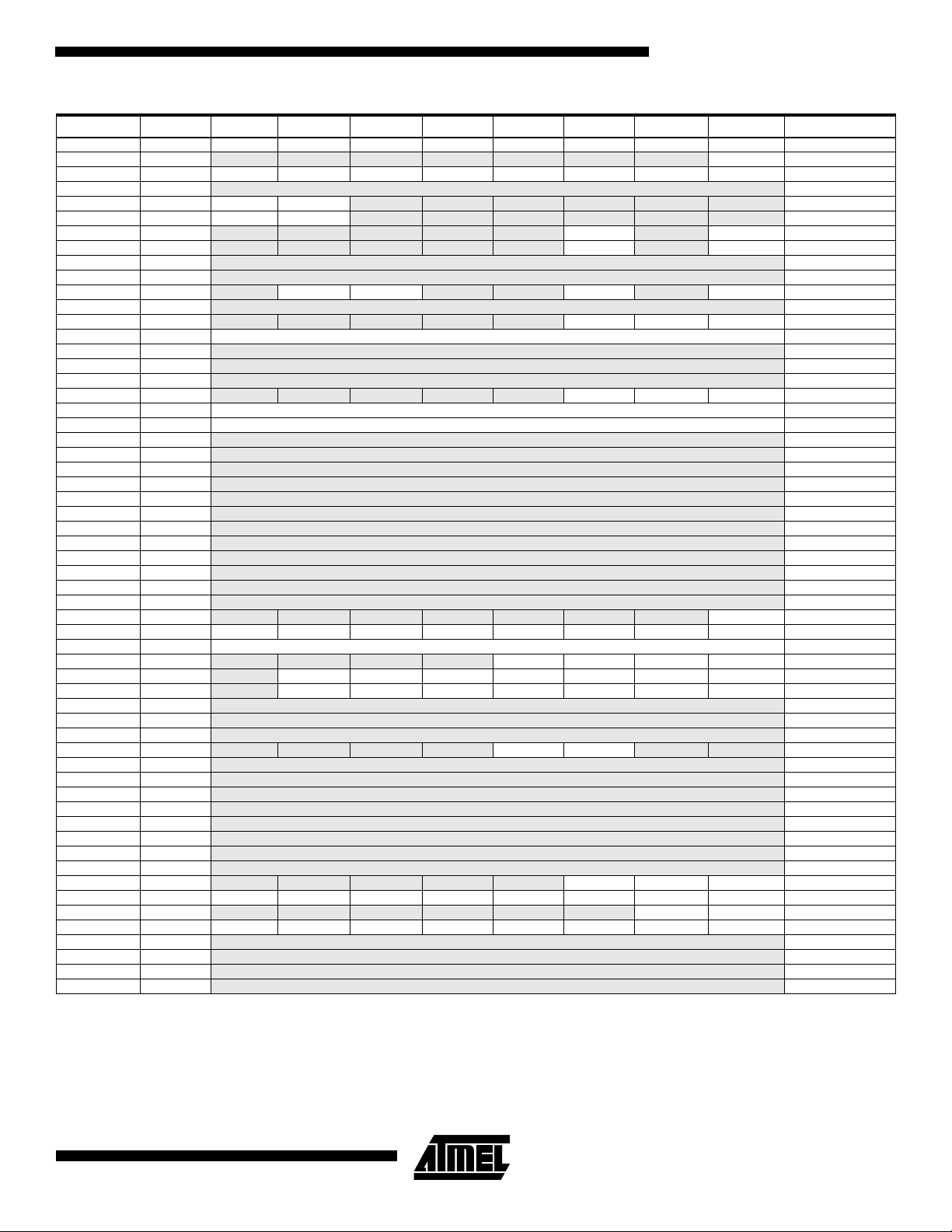
AT90C8534
AT90C8534 Register Summary
Address Name Bit 7 Bit 6 Bit 5 Bit 4 Bit 3 Bit 2 Bit 1 Bit 0 Page
$3F ($5F) SREG I T H S V N Z C page 17
$3E ($5E) SPH
$3D ($5D) SPL SP7 SP6 SP5 SP4 SP3 SP2 SP1 SP0 page 17
$3C ($5C) Reserved
$3B ($5B) GIMSK INT1 INT0 - - - - - - page 21
$3A ($5A) GIFR INTF1 INTF0
$39 ($59) TIMSK
$38 ($58) TIFR
$37 ($57) Reserved
$36 ($56) Reserved
$35 ($55) MCUCR -SESM - -ISC1 - ISC0 page 23
$34 ($54) Reserved
$33 ($53) TCCR0 - - - - - CS02 CS01 CS00 page 25
$32 ($52) TCNT0 Timer/Counter0 (8 Bits) page 26
$31 ($51) Reserved
$30 ($50) Reserved
$2F ($4F) Reserved
$2E ($4E) TCCR1 - - - - - CS12 CS11 CS10 page 26
$2D ($4D) TCNT1H Timer/Counter1 - Counter Register High Byte page 27
$2C ($4C) TCNT1L Timer/Counter1 - Counter Register Low Byte page 27
$2B ($4B) Reserved
$2A ($4A) Reserved
$29 ($49) Reserved
$28 ($48) Reserved
$27 ($47) Reserved
$26 ($46) Reserved
$25 ($45) Reserved
$24 ($44) Reserved
$23 ($43) Reserved
$22 ($42) Reserved
$21 ($41) Reserved
$20 ($40) Reserved
$1F ($3F) EEARH - - - - - - - EEAR8 page 28
$1E ($3E) EEARL EEAR7 EEAR6 EEAR5 EEAR4 EEAR3 EEAR2 EEAR1 EEAR0 page 28
$1D ($3D) EEDR EEPROM Data Register page 28
$1C ($3C) EECR
$1B ($3B) PORTA
$1A ($3A) DDRA
$19 ($39) Reserved
… Reserved
$11 ($11) Reserved
$10 ($30) GIPR - - - - IPIN1 IPIN0 - - page 21
$0F ($2F) Reserved
$0E ($2E) Reserved
$0D ($2D) Reserved
$0C ($2C) Reserved
$0B ($2B) Reserved
$0A ($2A) Reserved
$09 ($29) Reserved
$08 ($28) Reserved
$07 ($27) ADMUX - - - - - MUX2 MUX1 MUX0 page 34
$06 ($26) ADCSR ADEN ADSC ADRF ADIF ADIE ADPS2 ADPS1 ADPS0 page 34
$05 ($25) ADCH
$04 ($24) ADCL ADC7 ADC6 ADC5 ADC4 ADC3 ADC2 ADC1 ADC0 page 35
$03 ($20) Reserved
$02 ($22) Reserved
$01 ($21) Reserved
$00 ($20) Reserved
Note: For compatibility with future devices, reserved bits should be written to zero if accessed. Reserved I/O memory addresses
should never be written.
- - - - - - - SP8 page 17
page 21
- - - - -TOIE1 - TOIE0 page 22
- - - - -TOV1- TOV0 page 22
- - - - EERIE EEMWE EEWE EERE page 28
- PORTA6 PORTA5 PORTA4 PORTA3 PORTA2 PORTA1 PORTA0 page 37
- DDA6 DDA5 DDA4 DDA3 DDA2 DDA1 DDA0 page 37
- - - - - - ADC9 ADC8 page 35
49
Page 50

Instruction Set Summary
Mnemonic Operands Description Operation Flags # Clocks
ARITHMETIC AND LOGIC INSTRUCTIONS
ADD Rd, Rr Add Two Registers Rd ← Rd + Rr Z,C,N,V,H 1
ADC Rd, Rr Add with Carry Two Registers Rd
ADIW Rdl, K Add Immediate to Word Rdh:Rdl
SUB Rd, Rr Subtract Two Registers Rd
SUBI Rd, K Subtract Constant from Register Rd
SBC Rd, Rr Subtract with Carry Two Registers Rd
SBCI Rd, K Subtract with Carry Constant from Reg. Rd
SBIW Rdl, K Subtract Immediate from Word Rdh:Rdl
AND Rd, Rr Logical AND Registers Rd
ANDI Rd, K Logical AND Register and Constant Rd
OR Rd, Rr Logical OR Registers Rd
ORI Rd, K Logical OR Register and Constant Rd
EOR Rd, Rr Exclusive OR Registers Rd
COM Rd One’s Complement Rd
NEG Rd Two’s Complement Rd
SBR Rd, K Set Bit(s) in Register Rd
CBR Rd, K Clear Bit(s) in Register Rd
INC Rd Increment Rd
DEC Rd Decrement Rd
TST Rd Test for Zero or Minus Rd
CLR Rd Clear Register Rd
SER Rd Set Register Rd
BRANCH INSTRUCTIONS
RJMP k Relative Jump PC
IJMP Indirect Jump to (Z) PC
RCALL k Relative Subroutine Call PC
ICALL Indirect Call to (Z) PC
RET Subroutine Return PC
RETI Interrupt Return PC
CPSE Rd, Rr Compare, Skip if Equal if (Rd = Rr) PC
CP Rd, Rr Compare Rd - Rr Z,N,V,C,H 1
CPC Rd, Rr Compare with Carry Rd - Rr - C Z,N,V,C,H 1
CPI Rd, K Compare Register with Immediate Rd - K Z,N,V,C,H 1
SBRC Rr, b Skip if Bit in Register Cleared if (Rr(b) = 0) PC
SBRS Rr, b Skip if Bit in Register is Set if (Rr(b) = 1) PC
SBIC P, b Skip if Bit in I/O Register Cleared if (P(b) = 0) PC
SBIS P, b Skip if Bit in I/O Register is Set if (P(b) = 1) PC
BRBS s, k Branch if Status Flag Set if (SREG(s) = 1) then PC
BRBC s, k Branch if Status Flag Cleared if (SREG(s) = 0) then PC
BREQ k Branch if Equal if (Z = 1) then PC
BRNE k Branch if Not Equal if (Z = 0) then PC
BRCS k Branch if Carry Set if (C = 1) then PC
BRCC k Branch if Carry Cleared if (C = 0) then PC
BRSH k Branch if Same or Higher if (C = 0) then PC
BRLO k Branch if Lower if (C = 1) then PC
BRMI k Branch if Minus if (N = 1) then PC
BRPL k Branch if Plus if (N = 0) then PC
BRGE k Branch if Greater or Equal, Signed if (N
BRLT k Branch if Less than Zero, Signed if (N
BRHS k Branch if Half-carry Flag Set if (H = 1) then PC
BRHC k Branch if Half-carry Flag Cleared if (H = 0) then PC
BRTS k Branch if T-flag Set if (T = 1) then PC
BRTC k Branch if T-flag Cleared if (T = 0) then PC
BRVS k Branch if Overflow Flag is Set if (V = 1) then PC
BRVC k Branch if Overflow Flag is Cleared if (V = 0) then PC
BRIE k Branch if Interrupt Enabled if ( I = 1) then PC
BRID k Branch if Interrupt Disabled if ( I = 0) then PC
← Rd + Rr + C Z,C,N,V,H 1
← Rdh:Rdl + K Z,C,N,V,S 2
← Rd - Rr Z,C,N,V,H 1
← Rd - K Z,C,N,V,H 1
← Rd - Rr - C Z,C,N,V,H 1
← Rd - K - C Z,C,N,V,H 1
← Rdh:Rdl - K Z,C,N,V,S 2
←Rd • Rr Z,N,V 1
← Rd •K Z,N,V 1
← Rd v Rr Z,N,V 1
←Rd v K Z,N,V 1
← Rd ⊕ Rr Z,N,V 1
← $FF - Rd Z,C,N,V 1
← $00 - Rd Z,C,N,V,H 1
← Rd v K Z,N,V 1
← Rd • ($FF - K) Z,N,V 1
← Rd + 1 Z,N,V 1
← Rd - 1 Z,N,V 1
← Rd • Rd Z,N,V 1
← Rd ⊕ Rd Z,N,V 1
← $FF None 1
← PC + k + 1 None 2
← Z None 2
← PC + k + 1 None 3
← ZNone3
← STACK None 4
← STACK I 4
← PC + 2 or 3 None 1/2
← PC + 2 or 3 None 1/2
← PC + 2 or 3 None 1/2
← PC + 2 or 3 None 1/2
← PC + 2 or 3 None 1/2
←PC + k + 1 None 1/2
←PC + k + 1 None 1/2
← PC + k + 1 None 1/2
← PC + k + 1 None 1/2
← PC + k + 1 None 1/2
← PC + k + 1 None 1/2
← PC + k + 1 None 1/2
← PC + k + 1 None 1/2
← PC + k + 1 None 1/2
← PC + k + 1 None 1/2
⊕ V = 0) then PC ← PC + k + 1 None 1/2
⊕ V = 1) then PC ← PC + k + 1 None 1/2
← PC + k + 1 None 1/2
← PC + k + 1 None 1/2
← PC + k + 1 None 1/2
← PC + k + 1 None 1/2
← PC + k + 1 None 1/2
← PC + k + 1 None 1/2
← PC + k + 1 None 1/2
← PC + k + 1 None 1/2
50
AT90C8534
Page 51

AT90C8534
Instruction Set Summary (Continued)
Mnemonic Operands Description Operation Flags # Clocks
DATA TRANSFER INSTRUCTIONS
MOV Rd, Rr Move between Registers Rd
LDI Rd, K Load Immediate Rd
LD Rd, X Load Indirect Rd
LD Rd, X+ Load Indirect and Post-inc. Rd
LD Rd, -X Load Indirect and Pre-dec. X
LD Rd, Y Load Indirect Rd
LD Rd, Y+ Load Indirect and Post-inc. Rd
LD Rd, -Y Load Indirect and Pre-dec. Y
LDD Rd, Y+q Load Indirect with Displacement Rd
LD Rd, Z Load Indirect Rd
LD Rd, Z+ Load Indirect and Post-inc. Rd
LD Rd, -Z Load Indirect and Pre-dec. Z
LDD Rd, Z+q Load Indirect with Displacement Rd
LDS Rd, k Load Direct from SRAM Rd
ST X, Rr Store Indirect (X)
ST X+, Rr Store Indirect and Post-inc. (X)
ST -X, Rr Store Indirect and Pre-dec. X
ST Y, Rr Store Indirect (Y)
ST Y+, Rr Store Indirect and Post-inc. (Y)
ST -Y, Rr Store Indirect and Pre-dec. Y
STD Y+q, Rr Store Indirect with Displacement (Y + q)
ST Z, Rr Store Indirect (Z)
ST Z+, Rr Store Indirect and Post-inc. (Z)
ST -Z, Rr Store Indirect and Pre-dec. Z
STD Z+q, Rr Store Indirect with Displacement (Z + q)
STS k, Rr Store Direct to SRAM (k)
LPM Load Program Memory R0
IN Rd, P In Port Rd
OUT P, Rr Out Port P
PUSH Rr Push Register on Stack STACK
POP Rd Pop Register from Stack Rd
BIT AND BIT-TEST INSTRUCTIONS
SBI P, b Set Bit in I/O Register I/O(P,b)
CBI P, b Clear Bit in I/O Register I/O(P,b)
LSL Rd Logical Shift Left Rd(n+1)
LSR Rd Logical Shift Right Rd(n)
ROL Rd Rotate Left through Carry Rd(0)
ROR Rd Rotate Right through Carry Rd(7)
ASR Rd Arithmetic Shift Right Rd(n)
SWAP Rd Swap Nibbles Rd(3..0)
BSET s Flag Set SREG(s)
BCLR s Flag Clear SREG(s)
BST Rr, b Bit Store from Register to T T
BLD Rd, b Bit load from T to Register Rd(b)
SEC Set Carry C
CLC Clear Carry C
SEN Set Negative Flag N
CLN Clear Negative Flag N
SEZ Set Zero Flag Z
CLZ Clear Zero Flag Z
SEI Global Interrupt Enable I
CLI Global Interrupt Disable I
SES Set Signed Test Flag S
CLS Clear Signed Test Flag S
SEV Set Two’s Complement Overflow V
CLV Clear Two’s Complement Overflow V
SET Set T in SREG T
CLT Clear T in SREG T
SEH Set Half-carry Flag in SREG H
CLH Clear Half-carry Flag in SREG H
NOP No Operation None 1
SLEEP Sleep (see specific descr. for Sleep function) None 3
WDR Watchdog Reset this command has no effect None 1
← Rr None 1
← KNone1
← (X) None 2
← (X), X ← X + 1 None 2
← X - 1, Rd ← (X) None 2
← (Y) None 2
← (Y), Y ← Y + 1 None 2
← Y - 1, Rd ← (Y) None 2
← (Y + q) None 2
← (Z) None 2
← (Z), Z ← Z + 1 None 2
← Z - 1, Rd ← (Z) None 2
← (Z + q) None 2
← (k) None 2
← Rr None 2
← Rr, X ← X + 1 None 2
← X - 1, (X) ← Rr None 2
← Rr None 2
← Rr, Y ← Y + 1 None 2
← Y - 1, (Y) ← Rr None 2
← Rr None 2
← Rr None 2
← Rr, Z ← Z + 1 None 2
← Z - 1, (Z) ← Rr None 2
← Rr None 2
← Rr None 2
← (Z) None 3
← PNone1
← Rr None 1
← Rr None 2
← STACK None 2
← 1None2
← 0None2
← Rd(n), Rd(0) ← 0 Z,C,N,V 1
← Rd(n+1), Rd(7) ← 0 Z,C,N,V 1
←C, Rd(n+1) ← Rd(n), C ←Rd(7) Z,C,N,V 1
←C, Rd(n) ← Rd(n+1), C ←Rd(0) Z,C,N,V 1
← Rd(n+1), n = 0..6 Z,C,N,V 1
←Rd(7..4), Rd(7..4) ←Rd(3..0) None 1
← 1 SREG(s) 1
← 0 SREG(s) 1
← Rr(b) T 1
← TNone1
← 1C1
← 0C1
← 1N1
← 0N1
← 1Z1
← 0Z1
← 1I1
← 0I1
← 1S1
← 0S1
← 1V1
← 0V1
← 1T1
← 0T1
← 1H1
← 0H1
51
Page 52

Ordering Information
Speed (MHz) Power Supply Ordering Code Package Operation Range
1.5 3.3 - 6.0V AT90C8534-1AC 48A Commercial
(0°C to 70°C)
1.5 3.3 - 6.0V AT90C8534-1AI 48A Industrial
(-40°C to 85°C)
Package Type
48A 48-lead, Thin (1.0 mm) Plastic Gull Wing Quad Flat Package (TQFP)
52
AT90C8534
Page 53

Packaging Information
48A, 48-lead, Thin (1.0 mm) Plastic Gull Wing Quad
Flat Package (TQFP)
Dimensions in Millimeters and (Inches)*
AT90C8534
PIN 1 ID
0.50(0.020) BSC
0˚
0.20(.008)
0.09(.003)
7˚
0.75(0.030)
0.45(0.018)
0.15(0.006)
0.05(0.002)
*Controlling dimension: millimeters
9.25(.364)
8.75(.344)
7.1(0.280)
6.9(0.272)
SQ
0.27(0.011)
0.17(0.007)
SQ
1.60(0.063) MAX
53
Page 54

Atmel Headquarters Atmel Operations
Corporate Headquarters
2325 Orchard Parkway
San Jose, CA 95131
TEL (408) 441-0311
FAX (408) 487-2600
Europe
Atmel SarL
Route des Arsenaux 41
Casa Postale 80
CH-1705 Fribourg
Switzerland
TEL (41) 26-426-5555
FAX (41) 26-426-5500
Asia
Atmel Asia, Ltd.
Room 1219
Chinachem Golden Plaza
77 Mody Road Tsimhatsui
East Kowloon
Hong Kong
TEL (852) 2721-9778
FAX (852) 2722-1369
Japan
Atmel Japan K.K.
9F, Tonetsu Shinkawa Bldg.
1-24-8 Shinkawa
Chuo-ku, Tokyo 104-0033
Japan
TEL (81) 3-3523-3551
FAX (81) 3-3523-7581
Atmel Colorado Springs
1150 E. Cheyenne Mtn. Blvd.
Colorado Springs, CO 80906
TEL (719) 576-3300
FAX (719) 540-1759
Atmel Rousset
Zone Industrielle
13106 Rousset Cedex
France
TEL (33) 4-4253-6000
FAX (33) 4-4253-6001
Atmel Smart Card ICs
Scottish Enterprise Technology Park
East Kilbride, Scotland G75 0QR
TEL (44) 1355-803-000
FAX (44) 1355-242-743
Atmel Grenoble
Avenue de Rochepleine
BP 123
38521 Saint-Egreve Cedex
France
TEL (33) 4-7658-3000
FAX (33) 4-7658-3480
Fax-on-Demand
North America:
1-(800) 292-8635
International:
1-(408) 441-0732
e-mail
literature@atmel.com
Web Site
http://www.atmel.com
BBS
1-(408) 436-4309
© Atmel Corporation 2000.
Atmel Corporation makes no warranty for the use of its products, other than those expressly contained in the Company’s standard warranty which is detailed in Atmel’s Terms and Conditions located on the Company’s web site. The Company assumes no responsibility for
any errors which may appear in this document, reserves the right to change devices or specifications detailed herein at any time without
notice, and does not make any commitment to update the information contained herein. No licenses to patents or other intellectual property of Atmel are granted by the Company in connection with the sale of Atmel products, expressly or by implication. Atmel’s products are
not authorized for use as critical components in life support devices or systems.
Marks bearing ® and/or ™ are registered trademarks and trademarks of Atmel Corporation.
Terms and product names in this document may be trademarks of others.
Printed on recycled paper.
1229B–11/00/xM
 Loading...