

Page 1

Features
• Compatible with MCS-51
• 8K Bytes of In-System Programmable (ISP) Flash Memory
– Endurance: 1000 Write/Erase Cycles
• 4.0V to 5.5V Operating Range
• Fully Static Operation: 0 Hz to 33 MHz
• Three-level Program Memory Lock
• 256 x 8-bit Internal RAM
• 32 Programmable I/O Lines
• Three 16-bit Timer/Counters
• Eight Interrupt Sources
• Full Duplex UART Serial Channel
• Low-power Idle and Power-down Modes
• Interrupt Recovery from Power-down Mode
• Watchdog Timer
• Dual Data Pointer
• Power-off Flag
®
Products
8-bit
Microcontroller
with 8K Bytes
In-System
Description
The AT89S52 is a low-power, high-performance CMOS 8-bit microcontroller with 8K
bytes of in-system programmable Flash memory. The device is manufactured using
Atmel’s high-density nonvolatile memory technology and is compatible with the industry-standar d 80C51 instru ctio n set an d pino ut. The o n-chip Flash allow s the pro gram
memory to be reprogramme d in -s yste m or by a con ve nti ona l non vo lat il e mem or y pro grammer. By combin ing a versat ile 8-bit CPU wi th in-system program mable Flas h on
a monolithic chip, the Atmel AT89S52 is a powerful microcontroller which provides a
highly-flexible and cost-effective solution to many embedded control applications.
The AT89S52 provides the following standard features: 8K bytes of Flash, 256 bytes
of RAM, 32 I/O lines, Watchdog timer, two data pointers, three 16-bit timer/counters, a
six-vector two-level interrupt architecture, a full duplex serial port, on-chip oscillator,
and clock circuitry. In addition, the AT89S52 is designed with static logic for operation
down to zero frequency and supports two software selectable power saving modes.
The Idle Mode stops the CPU while allowing the RAM, timer/counters, serial port, and
interrupt system to co ntinue f unctio ning. T he Po wer-down mode s aves t he RAM con tents but freezes the oscillator, disabling all other chip functions until the next interrupt
or hardware reset.
Programmable
Flash
AT89S52
Rev. 1919A-07/01
1
Page 2

Pin Configurations
PDIP
PLCC
(T2) P1.0
(T2 EX) P1.1
P1.2
P1.3
P1.4
(MOSI) P1.5
(MISO) P1.6
(SCK) P1.7
RST
(RXD) P3.0
(TXD) P3.1
(INT0) P3.2
(INT1) P3.3
(T0) P3.4
(T1) P3.5
(WR) P3.6
(RD) P3.7
XTAL2
XTAL1
GND
1
2
3
4
5
6
7
8
9
10
11
12
13
14
15
16
17
18
19
20
TQFP
40
39
38
37
36
35
34
33
32
31
30
29
28
27
26
25
24
23
22
21
VCC
P0.0 (AD0)
P0.1 (AD1)
P0.2 (AD2)
P0.3 (AD3)
P0.4 (AD4)
P0.5 (AD5)
P0.6 (AD6)
P0.7 (AD7)
EA/VPP
ALE/PROG
PSEN
P2.7 (A15)
P2.6 (A14)
P2.5 (A13)
P2.4 (A12)
P2.3 (A11)
P2.2 (A10)
P2.1 (A9)
P2.0 (A8)
(MOSI) P1.5
(MISO) P1.6
(SCK) P1.7
RST
(RXD) P3.0
NC
(TXD) P3.1
(INT0) P3.2
(INT1) P3.3
(T0) P3.4
(T1) P3.5
P1.4
P1.3
P1.2
P1.1 (T2 EX)
P1.0 (T2)NCVCC
P0.0 (AD0)
65432
7
8
9
10
11
12
13
14
15
16
17
1819202122232425262728
(RD) P3.7
(WR) P3.6
XTAL2
XTAL1
GND
1
NC
4443424140
(A8) P2.0
(A9) P2.1
P0.1 (AD1)
P0.2 (AD2)
P0.3 (AD3)
39
38
37
36
35
34
33
32
31
30
29
(A10) P2.2
(A11) P2.3
(A12) P2.4
P0.4 (AD4)
P0.5 (AD5)
P0.6 (AD6)
P0.7 (AD7)
EA/VPP
NC
ALE/PROG
PSEN
P2.7 (A15)
P2.6 (A14)
P2.5 (A13)
(MOSI) P1.5
(MISO) P1.6
(SCK) P1.7
RST
(RXD) P3.0
NC
(TXD) P3.1
(INT0) P3.2
(INT1) P3.3
(T0) P3.4
(T1) P3.5
P1.4
P1.3
P1.2
P1.1 (T2 EX)
P1.0 (T2)NCVCC
4443424140393837363534
1
2
3
4
5
6
7
8
9
10
11
1213141516171819202122
GND
GND
XTAL2
XTAL1
(RD) P3.7
(WR) P3.6
P0.0 (AD0)
P0.1 (AD1)
(A8) P2.0
(A9) P2.1
(A10) P2.2
P0.2 (AD2)
P0.3 (AD3)
33
32
31
30
29
28
27
26
25
24
23
(A11) P2.3
(A12) P2.4
P0.4 (AD4)
P0.5 (AD5)
P0.6 (AD6)
P0.7 (AD7)
EA/VPP
NC
ALE/PROG
PSEN
P2.7 (A15)
P2.6 (A14)
P2.5 (A13)
2
AT89S52
Page 3
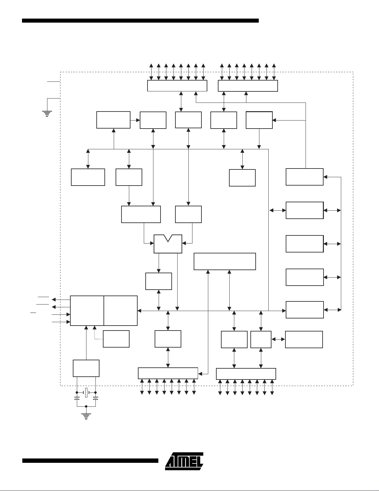
Block Diagram
AT89S52
V
CC
GND
B
REGISTER
RAM ADDR.
REGISTER
P0.0 - P0.7
PORT 0 DRIVERS
RAM
ACC
TMP2 TMP1
PORT 0
LATCH
PORT 2 DRIVERS
PORT 2
LATCH
POINTER
P2.0 - P2.7
FLASH
STACK
PROGRAM
ADDRESS
REGISTER
BUFFER
PSEN
ALE/PROG
EA / V
RST
PC
ALU
INTERRUPT, SERIAL PORT,
AND TIMER BLOCKS
PSW
TIMING
AND
PP
CONTROL
OSC
INSTRUCTION
REGISTER
WATCH
DOG
PORT 3
LATCH
PORT 3 DRIVERS
P3.0 - P3.7
PORT 1
LATCH
PORT 1 DRIVERS
P1.0 - P1.7
ISP
PORT
INCREMENTER
PROGRAM
COUNTER
DUAL DPTR
PROGRAM
LOGIC
3
Page 4

Pin Description
VCC
Supply voltage.
GND
Ground.
Port 0
Port 0 is an 8-bit open drain bidirectional I/O port. As an
output port, e ach pin can sink eight T TL inputs . When 1s
are written to port 0 pins, the pins can be used as highimpedance inputs.
Port 0 can also be conf igured to be the multiple xed loworder address/data bus during accesses to external
program and data memory. In this mode, P0 has internal
pullups.
Port 0 also receives the code bytes during Flash programming and outputs the code bytes during program ve rification. External pullups are required during program
verification.
Port 1
Port 1 is an 8 -bit bid irect iona l I/O port wi th inte rnal pullu ps.
The Port 1 output buffers can sink/source four TTL inputs.
When 1s are written to Port 1 pins, they are pulled high by
the internal pullups and can be used as inputs. As inputs,
Port 1 pins that are externally being pulled low will source
current (I
In addition, P1.0 and P1.1 can be configured to be the
timer/counter 2 external count input (P1.0/T2) and the
timer/counter 2 trigger input (P1.1/T2EX), respectively, as
shown in the following table.
Port 1 also receives the low-order address bytes during
Flash programming and verification.
Port Pin Alternate Functions
P1.0 T2 (external count input to Timer/Counter 2),
P1.1 T2EX (Timer/Counter 2 capture/reload trigger
P1.5 MOSI (used for In-System Progr amm ing )
P1.6 MISO (used for In-System Progr amm ing )
P1.7 SCK (used for In-System Programming)
Port 2
Port 2 is an 8 -bit bid irect iona l I/O port wi th inte rnal pullu ps.
The Port 2 output buffers can sink/source four TTL inputs.
When 1s are written to Port 2 pins, they are pulled high by
the internal pullups and can be used as inputs. As inputs,
Port 2 pins that are externally being pulled low will source
current (I
Port 2 emits the high-order address byte during fetches
from external program memory and during accesses to
) because of the internal pullups.
IL
clock-out
and direction control)
) because of the internal pullups.
IL
external data memor y th at u se 16-bi t ad dr es se s (MO V X @
DPTR). In this application, Port 2 uses strong internal pullups when emitting 1s. During accesses to external data
memory that use 8-bit addresses (MOVX @ RI), Port 2
emits the contents of the P2 Special Function Register.
Port 2 also receives the high-order address bits and some
control signals during Flash programming and verification.
Port 3
Port 3 is an 8-b it bi directi onal I/O po rt with i ntern al pull ups.
The Port 3 output buffers can sink/source four TTL inputs.
When 1s are written to Port 3 pins, they are pulled high by
the internal pullups and can be used as inputs. As inputs ,
Port 3 pins that are externally being pulled low will source
current (I
) because of the pullups.
IL
Port 3 also serv es t he fun ctions of variou s spec ial features
of the AT89S52, as shown in the following table.
Port 3 also receives some control signals for Flash programming and verification.
Port Pin Alternate Functions
P3.0 RXD (serial input port)
P3.1 TXD (serial output port)
P3.2 INT0
P3.3 INT1
P3.4 T0 (timer 0 external input)
P3.5 T1 (timer 1 external input)
P3.6 WR
P3.7 RD
(external interrupt 0)
(external interrupt 1)
(external data memory write strobe)
(external data memory read strobe)
RST
Reset input. A high on this pin for two machine cycles while
the oscillator is running resets the device. This pin drives
High for 96 oscillator pe riods a fter the W atc hdo g ti mes ou t.
The DISRTO bit in SFR AUXR (addre ss 8EH) ca n be used
to disable this feature. In the default state of bit DISRTO,
the RESET HIGH out feature is enabled.
ALE/PROG
Address Latch Ena ble ( ALE) is an out put p ulse for latc hing
the low byte of the address du ring accesse s to externa l
memory. This pin is also the program pulse input (PROG
during Flash programmin g.
In normal operation, ALE is emitted at a constant rate of
1/6 the oscil lator frequen cy and may be used for externa l
timing or cloc king purposes. N ote, however, th at one
ALE pulse is skipped during each acces s to external data
memory.
If desired, ALE operation can be disabled by setting bit 0 of
SFR location 8EH. With the bit set, ALE is active only during a MOVX or MOVC instruction. Otherwise, the pin is
)
4
AT89S52
Page 5

AT89S52
weakly pulled high. Setting the ALE-disable bit has no
effect if the microcontroller is in external execution mode.
PSEN
Program Store Enable (PSEN) is the read strobe to external program memory.
When the AT89S52 is executing code from external program memory, PSEN
cycle, except that two PSEN
is activated twice each machine
activations are skipped durin g
each access to external data memory.
EA
/VPP
External Access Enable. EA
must be strapped to GND in
Note, howev er, tha t if lo ck bit 1 is pro gramm ed, EA
internally latched on reset.
EA
should be strapped to VCC for internal program execu-
tions.
This pin also receives the 12-volt programming enable volt-
age (V
) during Flash programming.
PP
XTAL1
Input to the inverting os cillator amp lifier and input to the
internal clock operating circuit.
XTAL2
Output from the inverting oscill ator amplifier.
order to enable the device to fetch cod e from exter nal program memory locations starting at 0000H up to FFFFH.
Table 1. AT89S52 SFR Map and Reset Values
0F8H 0FFH
0F0H
0E8H 0EFH
0E0H
B
00000000
ACC
00000000
will be
0F7H
0E7H
0D8H 0DFH
0D0H
0C8H
0C0H 0C7H
0B8H
0B0H
0A8H
0A0H
98H
90H
88H
80H
PSW
00000000
T2CON
00000000
IP
XX000000
P3
11111111
IE
0X000000
P2
11111111
SCON
00000000
P1
11111111
TCON
00000000
P0
11111111SP00000111
T2MOD
XXXXXX00
SBUF
XXXXXXXX
TMOD
00000000
RCAP2L
00000000
AUXR1
XXXXXXX0
TL0
00000000
DP0L
00000000
RCAP2H
00000000
TL1
00000000
DP0H
00000000
TL2
00000000
TH0
00000000
DP1L
00000000
TH2
00000000
TH1
00000000
DP1H
00000000
WDTRST
XXXXXXXX
AUXR
XXX00XX0
PCON
0XXX0000
0D7H
0CFH
0BFH
0B7H
0AFH
0A7H
9FH
97H
8FH
87H
5
Page 6

Special Function Registers
A map of the on-chip memory area called the Special Function Register (SFR) space is shown in Table 1.
Note that not all of the addresses are occupied, and unoccupied addresses may not be implemented on the chip.
Read accesses to these addresses will in general return
random data, and write accesses will have an indeterminate effect.
User software should not write 1s to these unlisted locations, since they may be used in future products to invoke
Table 2. T2CON – Timer/Counter 2 Control Register
T2CON Address = 0C8H Reset Value = 0000 0000B
Bit Addressable
Bit TF2 EXF2 RCLK TCLK EXEN2 TR2 C/T2
76543210
Symbol Function
TF2 Timer 2 overflow flag set b y a Time r 2 overflow and mus t be cle ared b y softw ar e. TF2 will not be se t when eith er RCLK = 1
or TCLK = 1.
EXF2 Timer 2 external flag set when either a capture or reload is caused by a negative transition on T2EX and EXEN2 = 1.
When Timer 2 interrupt is enabled, EXF2 = 1 will cause the CPU to vector to the Timer 2 interrupt routine. EXF2 must be
cleared by software. EXF2 does not cause an interrupt in up/down counter mode (DCEN = 1).
RCLK Receive clock enable. When set, causes the serial port to use Timer 2 overflow pulses for its receive clock in serial port
Modes 1 and 3. RCLK = 0 causes Timer 1 overflow to be used for the receive clock.
new features. In th at case, the res et or inactiv e values of
the new bits will always be 0.
Timer 2 Registers: Control and status bits are contained in
registers T2CON (shown in Table 2) and T2MOD (shown in
Table 3) for Timer 2. The register pai r (RCAP 2H, RCAP 2L)
are the Capture/Reload registers for Timer 2 in 16-bit capture mode or 16-bit auto-reload mode.
Interrupt Registers: The individual interrupt enable bits
are in the IE register. Two priorities can be set for each of
the six interrupt sources in the IP register.
CP/RL2
TCLK Transmit clock enable. When set, causes the serial port to use Timer 2 overflow pulses for its transmit clock in serial port
Modes 1 and 3. TCLK = 0 causes Timer 1 overflows to be used for the transmit clock.
EXEN2 Timer 2 external enab le . Wh en set, allo ws a captu re o r reload to occur as a resul t of a ne gativ e trans ition on T2 EX if T imer
2 is not being used to clock the serial port. EXEN2 = 0 causes Timer 2 to ignore events at T2EX.
TR2 Start/Stop control for Timer 2. TR2 = 1 starts the timer.
C/T2
CP/RL2
Timer or counter select for Timer 2. C/T2 = 0 f or time r fun cti on. C/T2 = 1 for external event counter (falling edge triggered).
Capture/Reload select. CP/RL2 = 1 causes captures to occur on negative transitions at T2EX if EXEN2 = 1. CP/RL2 = 0
causes automatic re loa ds to oc c ur w he n Ti me r 2 o verflows or nega tive transitio ns o ccur a t T2EX when EXEN2 = 1. When
either RCLK or TCLK = 1, this bit is ignored and the timer is forced to auto-reload on Timer 2 overflow.
6
AT89S52
Page 7

AT89S52
Table 3a. AUXR: Auxiliary Register
AUXR Address = 8EH Reset Value = XXX00XX0B
Not Bit Addressable
– – – WDIDLE DISRTO – – DISALE
Bit 7 6 5 4 3 2 1 0
– Reserved for future expansion
DISALE Disable/Enable ALE
DISALE Operating Mode
0 ALE is emitted at a constant rate of 1/6 the oscillator frequency
1 ALE is act ive only during a MOVX or MOVC instruction
DISRTO Disable/Enable Reset out
DISRTO
0 Reset pin is driven High after WDT times out
1 Reset pin is input only
WDIDLE Disable/Enab le WDT in IDLE mode
WDIDLE
0 WDT continues to count in IDLE mode
1 WDT halts counting in IDLE mode
Dual Data Pointer Registers: To facilitat e acces sing bot h
internal and external data memory, two banks o f 16-bit
Data Pointer Registers are provided: DP0 at SFR address
locations 82H-83H and DP 1 at 84H-85H. Bit DPS = 0
in SFR AUXR 1 selects DP0 and DPS = 1 selects DP1.
The user should always initial ize the DPS bit to the
appropriate value before accessing the respective Data
Pointer Register.
Power Off Flag: The Power Off Flag (POF) is located at bit
4 (PCON.4) in the PCON SFR. POF is set to “1” during
power up. It can be set and rest under software control and
is not affected by reset.
Table 3b. AUXR1: Auxiliar y Regi ste r 1
AUXR1 Address = A2H Reset Value = XXXXXXX0B
Not Bit Addressable
–––– – – –DPS
Bit 7 6 5 4 3 2 1 0
– Reserved for future expansion
DPS Data Pointer Register Select
DPS
0 Selects DPTR Registers DP0L, DP0H
1 Selects DPTR Registers DP1L, DP1H
7
Page 8

Memory Organization
MCS-51 devices have a separate address space for Program and Data Memory. Up to 64K bytes each of external
Program and Data Memory can be addressed.
Program Memory
If the EA pin is connec ted to GND, all pr ogram f etches ar e
directed to external memory.
On the AT89S52, if EA
fetches to addresses 0000H through 1FFFH are directed to
internal memory and fetches to addresses 2000H through
FFFFH are to external memory.
Data Memory
The AT89S52 implements 256 bytes of on-chip RAM. The
upper 128 byte s occupy a para llel addr ess space to the
Special Function Reg is ter s. T hi s m ean s that the upp er 12 8
bytes have th e s ame addre sse s a s the SF R spac e b ut a re
physically separate from SFR space.
is connected to VCC, program
When an instruction accesses an internal location above
address 7FH, the address mode used in the instruction
specifies whether the CPU acces ses the upp er 128 bytes
of RAM or th e SFR sp ace. Ins tructions w hich us e direct
addressing access of the SFR space.
For example, the following direct addressing instruction
accesses the SFR at location 0A0H (which is P2).
MOV 0A0H, #data
Instructions that use indirect addressing access the upper
128 bytes of RAM. For example, the following indirect
addressing instru ct ion , wher e R0 co ntai ns 0A0 H, ac ce ss es
the data byte at a ddress 0A0H, rath er than P2 (whos e
address is 0A0H).
MOV @R0, #data
Note that stack operations are examples of indirect
addressing, so th e uppe r 128 bytes o f data RAM a re av ailable as stack space.
8
AT89S52
Page 9

AT89S52
Watchdog Timer (One-time Enabled with Reset-out)
The WDT is intended as a recovery method in situations
where the CPU may be subjected to software upsets. The
WDT consists of a 13-bit c ounter an d the Wat chdog Timer
Reset (WDTRST) SFR. The WDT is defaulted to disable
from exiting reset. To enable the WDT, a user must write
01EH and 0E1H in sequence to the WDTRST register
(SFR location 0A6H). When the WDT i s enabled, it will
increment every machine cycle whi le the o scillator i s running. The WDT timeout period is dependent on the external
clock frequenc y. There is no way to disab le the WDT
except through reset (either hardware reset or WDT overflow reset). When WDT overflows, it will drive an output
RESET HIGH pulse at the RST pin.
Using the WDT
To enable the WDT, a user must write 01EH and 0E1H in
sequence to the WDTRST register (SFR location 0A6H).
When the WDT is enabled, the user needs to service it by
writing 01EH and 0E1H to W DTRST to av oid a WDT overflow. The 13-bit counter overflows when it reach es 8191
(1FFFH), and this wi ll reset the device. When the W DT is
enabled, it will increment every machine cycle while the
oscillator is running. This means the user must reset the
WDT at least ev ery 8191 ma chine cycles . To reset th e
WDT the user must write 01EH and 0E1H to WDTRST.
WDTRST is a writ e-on ly r egi st er. T he W DT co unt er c anno t
be read or written. When WDT overflows, it will generate an
output RESET pulse at the RST pin. The RESET pulse
duration is 96xTO SC, whe re TOSC= 1/FOS C. To ma ke the
best use of the WDT, it should be serviced in those sections of code that will periodically be executed within the
time required to prevent a WDT reset.
WDT During Power-down and Idle
In Power-down mode the osci llato r s top s, whi c h mea ns th e
WDT also stops. While in Power-down mode, the user
does not need to service the WDT. There are tw o methods
of exiting Power-down mode: by a hardware reset or via a
level-activated exter nal inte rrupt whic h is enabl ed prior t o
entering Power-down mode. When Power-down is exited
with hardware reset, servicing the WDT should occur as it
normally does whe never the AT89S5 2 is reset. Exitin g
Power-down with an interrupt is significantly different. The
interrupt is held low long enough for the oscillator to stabilize. When the interrupt is brought high, the interrupt is
serviced. To prevent the WDT from resetting the device
while the interrupt pin is held low, the WDT is not started
until the interrupt is pulled high. It is suggested that the
WDT be reset during the interrupt service for the interrupt
used to exit Power-down mode.
To ensure that the WDT does not overflow within a few
states of exiting Power-down, it is best to reset the WDT
just before entering Power-down mode.
Before going into the IDLE mode , the WDIDLE bi t in SFR
AUXR is used to d eter mine w het her th e WD T c onti nues t o
count if enabled. The WDT keeps counting during IDLE
(WDIDLE bit = 0) as the de fault s tate. To pr event the WDT
from resetting the AT89S52 while in IDLE m ode, the u ser
should always set up a timer that will periodically exit IDLE,
service the WDT, and reenter IDLE mode.
With WDIDLE bit ena bled, the WDT will stop to count in
IDLE mode and resumes the count upon exit from IDLE.
UART
The UART in the AT89S52 operates the same way as the
UART in the AT89C51 and AT89C52. For further information on the UART operation, refer to the ATMEL Web site
(http://www.atmel.com). From the home page, select ‘Products’, then ‘805 1-Archite cture Flash M icrocontr oller’, then
‘Product Overview ’.
Timer 0 and 1
Timer 0 and Timer 1 in the AT89S52 operate the same way
as Timer 0 and Timer 1 in the AT89C51 and AT89C52. For
further information on the timers’ operation, refer to the
ATMEL Web site (http://www.atmel.com). From the hom e
page, select ‘Products’, then ‘8051-Architecture Flash
Microcontroller’, then ‘Product Overview’.
Timer 2
Timer 2 is a 16-bit Timer/Counter that can operate as either
a timer or an event counter. The type of operation is
selected by bit C/T2
Timer 2 has three operating modes: capture, auto-reload
(up or down counting), and baud rate generator. The
modes are selected by bits in T2CON, as shown in Table 3.
Timer 2 consists of two 8- bi t regis te rs, T H2 a nd TL2. In the
Timer function, th e TL2 register is incremented e very
machine cycl e. S ince a ma chine cy cle cons ists o f 1 2 os cillator periods, the count rate is 1/12 of the oscillator
frequency.
Table 3. Timer 2 Operating Modes
RCLK +TCLK CP/RL2 TR2 MODE
0 0 1 16-bit Auto-reload
0 1 1 16-bi t Capture
1 X 1 Baud Rate Generator
X X 0 (Off)
in the SFR T2CON (shown in Table 2).
9
Page 10

In the Counter function, the register is incremented in
response to a 1-to-0 transition at its corresponding external
input pin, T2. In this function, the external input is sampled
during S5P2 of every machine cycle. When the samples
show a high in one cycle and a low in the next cycle, the
count is incremented. The new count value appears in the
register during S3P1 of the cycle following the one in which
the transition was detected. Since two machine cycles (24
oscillator periods ) ar e required to recognize a 1- to-0 tra ns ition, the maximum count rate is 1/24 of the oscillator frequency. To ensure that a given l evel is sampl ed at least
once before it changes, the level should be held for at least
one full machine cycle.
Capture Mode
In the capture mode, two options ar e selected by bit
EXEN2 in T2CON. If EXEN2 = 0, Timer 2 is a 16-bit timer
or counter which upon overflow sets bit TF2 in T2CON.
Figure 5. Timer in Capture Mode
This bit can then be used to generate an interrupt. If
EXEN2 = 1, Timer 2 performs the same ope ratio n, but a 1to-0 transition at external input T 2EX also causes the
current value in TH2 and TL2 to be captured into RCAP2H
and RCAP2L, respectively. In addition, the transition at
T2EX cause s bit EXF2 i n T2CO N to be set. The EX F2 bit ,
like TF2, can generate an interrupt. The capture mode is
illustrated in Figur e 5.
Auto-reload (Up or Down Counter)
Timer 2 can be programmed to count up or down when
configured in its 16-bit auto-reload mode. This feature is
invoked by the DCEN (Down Counter Enable) bit located in
the SFR T2MOD (see Table 4). Upon reset, the DCEN bit
is set to 0 so that timer 2 will default to count up. When
DCEN is set, Timer 2 can count up or down, d ependi ng on
the value of the T2EX pin.
OSC
T2 PIN
T2EX PIN
÷12
TRANSITION
DETECTOR
C/T2 = 0
C/T2 = 1
EXEN2
TR2
CAPTURE
CONTROL
Figure 6 shows Timer 2 automatically counting up when
DCEN=0. In this mode, two option s are selected by bit
EXEN2 in T2CON. If EXEN2 = 0, Timer 2 counts up to
0FFFFH and then sets the TF2 b it upon overflow. The
overflow also causes the timer registers to be reloaded with
the 16-bit value in RCAP2H and RCAP2L. The values in
Timer in Capture ModeRCAP2H and RCAP2L are preset
by software. If EXEN2 = 1, a 16-bit rel oad c an be tr igge re d
either by an overflow or by a 1-to-0 transition at external
input T2EX. This transitio n al so s ets the EX F2 bit. Both the
TF2 and EXF2 bits can generate an interrupt if enabled.
Setting the DCEN bit enab le s T imer 2 to cou nt up or down ,
as shown in Figure 6. In this mode, the T2EX pin controls
TH2 TL2
CONTROL
RCAP2LRCAP2H
EXF2
TF2
OVERFLOW
TIMER 2
INTERRUPT
the direction of the count. A logic 1 at T2EX makes Timer 2
count up. The timer will ov erflow at 0FFFFH a nd set the
TF2 bit. This overflow also causes the 16-bit value in
RCAP2H and RCAP2L to be reloaded into the timer registers, TH2 and TL2, respectively.
A logic 0 at T2EX makes Timer 2 count down. The timer
underflows when TH2 and TL 2 equal the values stor ed in
RCAP2H and RCAP2L. The underflow sets the TF2 bit and
causes 0FFFFH to be reloaded into the timer registers.
The EXF2 bit toggles whenever Timer 2 overflows or
underflows and can be used as a 17th bit of resolution. In
this operating mode, EXF2 does not flag an interrupt.
10
AT89S52
Page 11
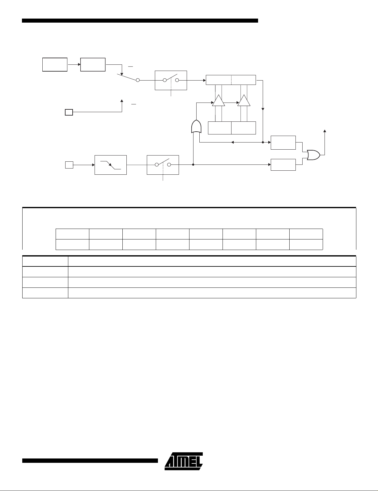
Figure 6. Timer 2 Auto Reload Mode (DCEN = 0)
AT89S52
OSC
T2 PIN
T2EX PIN
÷12
TRANSITION
DETECTOR
C/T2 = 0
C/T2 = 1
EXEN2
CONTROL
TR2
RELOAD
CONTROL
TH2 TL2
OVERFLOW
RCAP2LRCAP2H
TF2
EXF2
Table 4. T2MOD – Timer 2 Mode Control Register
T2MOD Address = 0C9H Reset Value = XXXX XX00B
Not Bit Addressable
––––––T2OEDCEN
TIMER 2
INTERRUPT
Bit76543210
Symbol Function
– Not implemented, reserved for future
T2OE Timer 2 Output Enable bit
DCEN When set, this bit allows Timer 2 to be configured as an up/down counter
11
Page 12

Figure 7. Timer 2 Auto Reload Mode (DCEN = 1)
(DOWN COUNTING RELOAD VALUE)
0FFH0FFH
TOGGLE
EXF2
OSC
12
÷
T2 PIN
C/T2 = 0
TR2
C/T2 = 1
Figure 8. Timer 2 in Baud Rate Generator Mode
NOTE: OSC. FREQ. IS DIVIDED BY 2, NOT 12
OVERFLOW
TH2 TL2
CONTROL
RCAP2LRCAP2H
(UP COUNTING RELOAD VALUE)
COUNT
DIRECTION
1=UP
0=DOWN
T2EX PIN
TIMER 1 OVERFLOW
2
÷
"0"
TF2
TIMER 2
INTERRUPT
"1"
SMOD1
OSC
T2 PIN
T2EX PIN
2
÷
TRANSITION
DETECTOR
C/T2 = 0
C/T2 = 1
TR2
EXEN2
CONTROL
CONTROL
TH2 TL2
RCAP2LRCAP2H
EXF2
"1"
"1"
TIMER 2
INTERRUPT
"0"
"0"
RCLK
16
÷
TCLK
÷
16
Rx
CLOCK
Tx
CLOCK
12
AT89S52
Page 13

Baud Rate Generator
Timer 2 is sele cted as the ba ud rate ge nerator b y setting
TCLK and/or RCLK in T2CON (Table 2). Note that the
baud rates for transmit and receive can be different if Timer
2 is used for the receiver or transmitter and Timer 1 is used
for the other functi on. Setting RCLK and/or TCLK puts
Timer 2 into its baud rate generator mode, as shown in Figure 8.
The baud rate generator mode is similar to th e auto-reloa d
mode, in that a rollover in TH2 causes the Timer 2 registers
to be reloaded with the 16-bit value in registers RCAP2H
and RCAP2L, which are preset by software.
The baud rates in Mode s 1 and 3 are deter mined by Tim er
2’s overflow rate according to the following equation.
Modes 1 and 3 Baud Rates
The Timer can be configured for either timer or counter
operation. In most a pplications, i t is configu red for timer
operation (CP/T2
= 0). The timer o peration is different for
Timer 2 when it is used as a baud rate generator. Normally,
as a timer, it increments ever y machine cycl e (at 1/12 the
oscillator frequency ). As a bau d rate ge nerat or, howe ver, it
Timer 2 Overflow Rate
----------------------------------------------------------- -=
16
AT89S52
increments every state time (at 1/2 the oscillator frequency). The baud rate formula is given below.
Modes 1 and 3
---------------------------------------
Baud Rate
where (RCAP2H, RC AP2L) is the cont ent of R CAP2H an d
RCAP2L taken as a 16-bit unsigned integer.
Timer 2 as a baud rate generator is shown in Figure 8. This
figure is valid only if RCLK or TCLK = 1 in T2CON. Note
that a rollover in TH2 does not set TF2 and will not generate an interrupt. Note too, that if EXEN2 is set, a 1-to-0
transition in T2EX wi ll set EXF2 but will not cause a re load
from (RCAP2H, RCAP2L) to (TH2, TL2). Thus, when Timer
2 is in use as a baud rate gene rator, T2E X can be used as
an extra external interrupt.
Note that when Timer 2 is running (TR2 = 1) as a timer in
the baud rate generat or mode, TH2 or TL2 should not be
read from or written to. Under these conditions, the Timer is
incremented every state time, and the results of a read or
write may not be accurate. The RCAP2 registers may be
read but should not be written to, because a write might
overlap a reload and cause write and/or reload errors. The
timer should be turned off (clear TR2) before accessing the
Timer 2 or RCAP2 registers.
Oscillator Frequency
------------------------------------------------------------------------------------- -=
32 x [65536-RCAP2H,RCAP2L)]
Figure 9. Time r 2 in Clock-Out Mode
OSC
P1.0
(T2)
TRANSITION
DETECTOR
P1.1
(T2EX)
÷2
TR2
C/T2 BIT
EXF2
EXEN2
(8-BITS)
RCAP2L RCAP2H
÷2
TIMER 2
INTERRUPT
TL2
TH2
(8-BITS)
T2OE (T2MOD.1)
13
Page 14
Programmable Clock Out
A 50% duty cycle clock can be programmed to come out on
P1.0, as shown in Figure 9. This pin, besides being a regular I/O pin, has two alternate funct ions. It can be programmed to input the external cl ock for Tim er/Counte r 2 or
to output a 50% d uty cy cle cl ock rang ing fr om 61 Hz to 4
MHz at a 16 MHz operating frequency.
To configure the Timer/Counter 2 as a clock generator, bit
(T2CON.1) must be cleared and bit T2OE (T2MOD.1)
C/T2
must be set. Bit TR2 (T2CON.2) starts and stops the timer.
The clock-out frequency depends on the oscillator frequency and the reload value of Timer 2 capture registers
(RCAP2H, RCAP2L), as shown in the following equation.
Clock-Out Frequency
Oscillator Frequency
------------------------------------------------------------------------------------ -=
4 x [65536-(RCAP2H,RCAP2L)]
In the clock-out mode, Timer 2 roll-overs will not generate
an interrupt. This behavior is similar to when Timer 2 is
used as a baud-rate generator. It is possible to use Timer 2
as a baud-rate generator and a clock generator simultaneously. Note, h owever, tha t the baud-r ate and cloc k-out
frequencies ca nnot be de termi ned inde pendent ly fro m one
another since they both use RCAP2H and RCAP2L.
Interrupts
The AT89S52 has a total of six int erru pt ve cto r s: two ex ternal interrupts (INT0
ers 0, 1, and 2), and the serial port interrupt. These
interrupts are all shown in Figure 10.
Each of these interrupt sources can be individually enabled
or disabled by setting or clearin g a bit in Specia l Function
Register IE. IE also contains a global disable bit, EA, which
disables all interrupts at once.
Note that Table 5 shows that bit position IE.6 is unimplemented. In the AT89S52, bit position IE.5 is also unimplemented. User soft ware should not writ e 1s to these bit
positions, since they may be used in future AT89 products.
Timer 2 interrupt is g ene ra ted b y the logical OR of bits TF2
and EXF2 in register T2CON. Neither of these flags is
cleared by hardware when the service routine is vectored
to. In fact, t he service routi ne may have to determine
whether it was TF2 or EXF2 that generated the interrupt,
and that bit will have to be cleared in software.
The Timer 0 and Timer 1 flags, TF0 and TF1, are set at
S5P2 of the c ycle in wh ich the t imer s o verflo w. T he v alues
are then polled by the circuitry in the next cycle. However,
the Timer 2 flag, TF2, is set at S2P2 and is polled in the
same cycle in which the timer over flo ws.
and INT1), three timer interrupts (Tim-
Table 5. Interrupt Enable (IE) Register
(MSB) (LSB)
EA – ET2 ES ET1 EX1 ET0 EX0
Enable Bit = 1 enables the interrupt.
Enable Bit = 0 disables the interrupt.
Symbol Position Function
EA IE.7 Disables all interrupts. If EA = 0 ,
no interrupt is acknowledged. If
EA = 1, each interrupt source is
individually enabled or disabled
by setting or clearing its enable
bit.
– IE.6 Reserved.
ET2 IE.5 Timer 2 interrupt enable bit.
ES IE.4 Serial Port interrupt enable bit.
ET1 IE.3 Timer 1 interrupt enable bit.
EX1 IE.2 External interrupt 1 enable bit.
ET0 IE.1 Timer 0 interrupt enable bit.
EX0 IE.0 External interrupt 0 enable bit.
User software should never write 1s to unimplemented bits,
because they may be used in future AT89 products.
Figure 10. Interrupt Sources
0
INT0
TF0
INT1
TF1
TF2
EXF2
1
0
1
TI
RI
IE0
IE1
14
AT89S52
Page 15

AT89S52
Oscillator Characteristics
XTAL1 and XTAL2 ar e the inp ut and output, respect ively,
of an inverting amplifier that can be conf igured for use as
an on-chip oscillator, as shown in Figure 11. Either a quartz
crystal or ceramic resonator may be used. To drive the
device from an external clock so ur ce , XTAL2 should be left
unconnected while XTAL1 is driven, as shown in Figure 12.
There are no requirements on the duty cycle of the external
clock signal, since the input to the internal clocking circuitry
is through a divide-by-two flip-flop, but minimum and maximum voltage high and low time specifications must be
observed.
Idle Mode
In idle mode, the CPU puts itself to sleep while all the onchip perip herals re main act ive. The m ode is inv oked by
software. The content of the on-chip RAM and all the special functions registers remain unchanged durin g this
mode. The idle mode can be term inated by any enable d
interrupt or by a hardware reset.
Note that when idle mode is te rminated by a hardware
reset, the devi ce normally re sumes progra m execution
from where it left off, up to two machine cycles before the
internal reset algori thm takes control. On -chip hardware
inhibits access to i nterna l RAM in this ev ent, but acc ess to
the port pins is not inhibited. To eliminate the possibility of
an unexpected write to a port pin when idle mode is terminated by a reset, the instruction following the one that
invokes idle m ode s houl d n ot write to a port pin or to exter nal memory.
active long enoug h to allow the oscillator t o restart
and stabilize.
Figure 11. Oscillator Connections
C2
XTAL2
C1
XTAL1
GND
Note: C1, C2 = 30 pF ± 10 pF for Crystals
= 40 pF ± 10 pF for Ceramic Resonators
Figure 12. External Clock Drive Configuration
NC
EXTERNAL
OSCILLATOR
SIGNAL
XTAL2
XTAL1
Power-down Mode
GND
In the Power-down mode , the os ci llator i s sto pped, and the
instruction that invokes Power -down is the las t instructio n
executed. The on-chip RAM and Special Function Registers retain their values until the Power-down mode is terminated. Exit from Power-down mode can be initiated either
by a hardware reset or by an enabled exte rnal interrupt.
Reset redefines the SFR s b ut do es not change the on-chip
RAM. The reset should not be activated before V
CC
is
restored to its normal operating level and must be held
Table 6. Status of External Pins During Idle and Power-down Modes
Mode Program Memory ALE PSEN PORT0 PORT1 PORT2 PORT3
Idle Internal 1 1 Data Data Data Data
Idle External 1 1 Float Data Address Data
Power-down Internal 0 0 Data Data Data Data
Power-down External 0 0 Float Data Data Data
15
Page 16

Program Memory Lock Bits
The AT89S52 has three lock bits that can be le ft unprogrammed (U) or can be programmed (P) to obtain the additional features listed in the following table.
Table 7. Lock Bit Protection Modes
Program Lock Bits
LB1 LB2 LB3 Protection Type
1 U U U No program lock features
2 P U U MOVC instructions executed
from external program
memory are disabled from
fetching code bytes from
internal memory, EA
sampled and latched on reset,
and further programming of
the Flash memory is disabled
3 P P U Same as mode 2, but verify is
also disabled
4 P P P Same as mode 3, but external
execution is also disabled
When lock bit 1 is programmed, the logic level at the EA
is sampled and latched durin g reset. If the device is powered up without a reset, t he latch i nitialize s to a rando m
value and holds that value until reset is activated. The
latched value of EA
at that pin in order for the device to function properly.
must agree w ith the c urren t logi c leve l
is
pin
Programming the Flash – Parallel Mode
The AT89S52 is shipped with the on-chip Flash memory
array ready to be programme d. The pr o gr amm ing inte rfac e
needs a high-voltage (12- volt) progr am enable signa l and
is compatible with conventional third-party Flash or
EPROM programmers.
The AT89S52 code memory ar ray is programm ed byte-bybyte.
Programming Algorithm: Before programming the
AT89S52, the address , data, and contr ol sig nals shou ld be
set up according to the Flash programming mode table and
Figures 13 and 1 4. To pr ogram t he AT8 9S52, take the following steps:
1. Input the desired memory location on the address
lines.
2. Input the appropriate data byte on the data lines.
3. Activate the correct combination of control signals.
4. Raise EA
5. Pulse ALE/PROG
Flash array or the lock bits. The byte-write cycle is
self-timed and typically takes no more than 50 µs.
/VPP to 12V.
once to program a byte in the
Repeat steps 1 through 5, changing the address
and data for the entire array or until the end of the
object file is reached.
Polling: The AT89S52 features Data Polling to indi-
Data
cate the end of a byte write cycle. During a write cycle, an
attempted read of the last byte written will result in the complement of the writte n data on P0.7 . Once the writ e cycle
has been completed, true data is valid on all outputs, and
the next cycle may begin . Data
after a write cycle has been initiated.
Ready/Busy
be monitored by the RDY/BS Y
low after ALE goes high during programming to indica te
BUSY
done to indicate READY.
Program Verify: If lock bits LB1 and LB2 have not been
programmed, the programmed code data can be read back
via the address and data lines for verification. The status of
the individual lock bits can be verified directly by reading
them back.
Reading the Signature Bytes: The signature bytes are
read by the same procedure as a normal verification of
locations 000H, 100H, and 200H, except that P3.6 a nd
P3.7 must be pulled to a logic low. T he va lu es r eturn ed ar e
as follows.
(000H) = 1EH indicates manufactured by Atmel
(100H) = 52H indicates 89S52
(200H) = 06H
Chip Erase: In the paral lel programming mode, a chip
erase operation is initiated by using the proper combination
of control signals and by pulsing ALE/PROG
tion of 200 ns - 500 ns.
In the serial programming mode, a chip erase operation is
initiated by issuing the Chip Erase instruction. In this mode,
chip erase is self-timed and takes about 500 ms.
During chip erase, a serial read from any address location
will return 00H at the data output.
: The progress of byte programming can also
. P3.0 is pulled high again when pro gramming is
Polling may begin any time
output signal. P3.0 is pul le d
low for a dura-
Programming the Flash – Serial Mode
The Code memory array can be programmed using the
serial ISP interface while RST is pulled to V
interface consists of pins SCK, MOSI (input) and MISO
(output). After RST is set high, the Programming Enable
instruction ne eds to be execu ted first befo re other operations can be executed. Before a reprogramming sequence
can occur, a Chip Erase operation is required.
The Chip Erase operation turns the content of every memory location in the Code array into FFH.
Either an external system clock can be supplied at pin
XTAL1 or a crystal needs to be connected across pins
XTAL1 and XTAL2. The maximum serial clock (SCK)
. The serial
CC
16
AT89S52
Page 17

AT89S52
frequency should be less than 1/16 of the crystal frequency. With a 33 MHz os c il lator cl oc k, the max im um SCK
frequency is 2 MHz.
Serial Programming Algorithm
To program and verify the AT89S52 in the serial programming mode, the following sequence is recommended:
1. Power-up sequence:
Apply power between VCC and GND pins.
Set RST pin to “H”.
If a crystal is not connected across pins XTAL1 and
XTAL2, apply a 3 MHz to 33 MHz clock to XTAL1 pin
and wait for at least 10 milliseconds.
2. Enable serial programming by sending the Programming Enable serial instruction to pin
MOSI/P1.5. The frequency of the shift clock supplied at pin SCK/P1.7 needs to be less than the
CPU clock at XTAL1 divided by 16.
3. The Code array is programmed one byte at a time
by supplying the address and data together with the
appropriate Write instruction. The write cycle is selftimed and typically takes less than 1 ms at 5V.
4. Any memory location can be verified by using the
Read instruction which returns the content at the
selected address at serial output MISO/P1.6.
5. At the end of a programming session, RST can be
set low to commence normal device operation.
Power-off sequence (if needed):
Set XTAL1 to “L” (if a crystal is not used).
Set RST to “L”.
Turn V
Data Polling: The Data Polling feature is also available in
the serial mode. In this mode, during a write cycle an
attempted read of the last byte written will result in the complement of the MSB of the serial output byte on MISO.
power off.
CC
Serial Programming Instruction Set
The Instruction Set for Serial Programming follows a 4-byte
protocol and is shown in Table 10.
17
Page 18

Programming Interface – Parallel Mode
Every code byte in the Flash array can be programmed by
using the appropriate combination of control signals. The
write operation cycle is self-timed and once initiated, will
automatically time itself to completion.
Table 8. Flash Programming Mod es
Mode V
CC
RST PSEN
Write Code Data 5V H L
ALE/
PROG
EA/
V
PP
(2)
12VLHHHH DINA12-8 A7-0
All major programmi ng ven dors off er wor ldwid e supp ort for
the Atmel microcontroller series. Please contact your local
programming vendor for the appropriate software revision.
P2.4-0 P1.7-0
Address
P2.6 P2.7 P3.3 P3.6 P3.7
P0.7-0
Data
Read Code Data 5V H L H H L L L H H D
(3)
Write Lock Bit 1 5V H L
Write Lock Bit 2 5V H L
Write Lock Bit 3 5V H L
Read Lock Bits
1, 2, 3
5V H L H H H H L H L
Chip Erase 5V H L
12VHHHHH X X X
(3)
12V H H H L L X X X
(3)
12V H L H H L X X X
(1)
12VHLHLL X X X
OUT
P0.2,
P0.3,
P0.4
A12-8 A7-0
XX
Read Atmel ID 5V H L H H LLLLL1EHX 0000 00H
Read Device ID 5V H L H H LLLLL 52HX 0001 00H
Read Device ID 5V H L H H LLLLL 06HX 0010 00H
Notes: 1. Each PROG pulse is 200 ns - 500 ns for Chip Erase.
2. Each PROG
3. Each PROG
4. RDY/BSY
pulse is 200 ns - 500 ns for Write Code Data.
pulse is 200 ns - 500 ns for Write Lock Bits.
signal is output on P3.0 during programming.
5. X = don’t care.
Figure 13. Programming the Flash Memory
(Parallel Mode)
AT89S52
P1.0-P1.7
P2.0 - P2.4
P2.6
P2.7
P3.3
P3.6
P3.7
XTAL2 EA
V
ALE
P3.0
CC
P0
ADDR.
0000H/1FFFH
SEE FLASH
PROGRAMMING
MODES TABLE
3-33 MHz
A0 - A7
A8- A12
V
CC
PGM
DATA
PROG
V/V
IH PP
RDY/
BSY
Figure 14. Verifying the Flash Memory (Parallel Mode)
V
P0
CC
CC
PGM DATA
(USE 10K
PULLUPS)
V
IH
ADDR.
0000H/1FFFH
SEE FLASH
PROGRAMMING
MODES TABLE
3-33 MHz
A0 - A7
A8- A12
AT89S52
P1.0-P1.7
P2.0 - P2.4
P2.6
P2.7
P3.3
P3.6
P3.7
XTAL2 EA
V
ALE
18
1
XTAL
GND
RST
PSEN
AT89S52
XTAL1
V
IH
GND
RST
PSEN
V
IH
Page 19

AT89S52
Flash Programming and Verification Characteristics (Parall el Mode)
TA = 20°C to 30°C, VCC = 4.5 to 5.5V
Symbol Parameter Min Max Units
V
PP
I
PP
I
CC
1/t
t
AVGL
t
GHAX
t
DVGL
t
GHDX
t
EHSH
t
SHGL
t
GHSL
t
GLGH
t
AVQV
t
ELQV
t
EHQZ
t
GHBL
t
WC
CLCL
Programming Supply Voltage 11.5 12.5 V
Programming Supp ly Curre nt 10 mA
VCC Supply Current 30 mA
Oscillator Frequency 3 33 MHz
Address Setup to PROG Low 48t
Address Hold After PROG 48t
Data Setup to PROG Low 48t
Data Hold After PROG 48t
P2.7 (ENABLE) High to V
PP
48t
CLCL
CLCL
CLCL
CLCL
CLCL
VPP Setup to PROG Low 10 µs
VPP Hold After PROG 10 µs
PROG Width 0.2 1 µs
Address to Data V al id 48t
ENABLE Low to Data Valid 48t
Data Float After ENABLE 048t
CLCL
CLCL
CLCL
PROG High to BUSY Low 1.0 µs
Byte Write Cycle Time 50 µs
Figure 15. Flash Programming and Verification Waveforms – Parallel Mode
P1.0 - P1.7
P2.0 - P2.5
P3.4
PORT 0
ALE/PROG
EA/V
PP
P2.7
(ENABLE)
P3.0
(RDY/BSY)
t
AVGL
t
SHGL
PROGRAMMING
ADDRESS
DATA IN
V
t
EHSH
t
PP
DVGL
t
GLGH
t
GHBL
t
GHDX
t
t
ELQV
GHAX
t
GHSL
LOGIC 1
LOGIC 0
BUSY
t
WC
VERIFICATION
ADDRESS
t
AVQV
DATA OUT
READY
t
EHQZ
19
Page 20

Figure 16. Flash Memory Serial Downloading
AT89S52
V
CC
V
CC
INSTRUCTION
INPUT
DATA OUTPUT
CLOCK IN
3-33 MHz
P1.5/MOSI
P1.6/MISO
P1.7/SCK
XTAL2
GND
RSTXTAL1
V
IH
Flash Programming and Verification Waveforms – Serial Mode
Figure 17. Serial Programming Waveforms
20
76543210
AT89S52
Page 21

Table 9. Serial Programming Instruction Set
Instruction
Format
AT89S52
Instruction
Programming Enable 1010 1100 0101 0011 xxxx xxxx xxxx xxxx
0110 1001
OperationByte 1 Byte 2 Byte 3 Byte 4
Enable Serial Programming
while RST is high
(Output)
Chip Erase 1010 1100 100x xxxx xxxx xxxx xxxx xxxx Chip Erase Flash memory
array
Read Program Memory
(Byte Mode)
Write Program Me mory
(Byte Mode)
Write Lock Bits
(2)
0010 0000 xxx Read data from Program
0100 0000 xxx Write data to Program
1010 1100 1110 00 xxxx xxxx xxxx xxxx Write Lock bits. See Note (2).
A9
A8
A11
A10
A12
A8
A9
A11
A10
A12
B2
B1
A7
A6
A7
A5
A6
A4
A5
A4
A3
A2A1A0
A3
A2
A1
A0
D7
D7
D6
D6
D5
D5
D4
D4
D3
D3
D2
D2
D0
D1
memory in the byte mode
D0
D1
memory in the byte mode
Read Lock Bits 0010 010 0 xxxx xxxx xxxx xxxx xx xx Read back current status of
LB1
LB2
LB3
the lock bits (a programmed
lock bit reads back as a ‘1’)
Read Signature Bytes
Read Program Memory
(Page Mode)
(1)
0010 1000 xxx xxx xxxx Signature Byte Read Signature Byte
0011 0000 xxx Byte 0 Byte 1...
A5
A12
A4A3A2
A11
A10
A9
A1
A8
A0
Byte 255
Read data from Program
memory in the Page Mode
(256 bytes)
Write Program Me mory
(Page Mode)
0101 0000 xxx Byte 0 Byte 1...
A9
A8
A11
A10
A12
Byte 255
Write data to Program
memory in the Page Mode
(256 bytes)
Notes: 1. The signature bytes are not readable in Lock Bit Modes 3 and 4.
2. B1 = 0, B2 = 0 ---> Mode 1, no lock protection
B1 = 0, B2 = 1 ---> Mode 2, lock bit 1 activated
B1 = 1, B2 = 0 ---> Mode 3, lock bit 2 activated
B1 = 1, B1 = 1 ---> Mode 4, lock bit 3 activated
}
After Reset signal is high, SCK should be low for at least 64
system clocks before it goes high to clock in the enable
data bytes. No pulsin g of Rese t signal is neces sary. SCK
should be no faster th an 1/16 of the system clock at
XTAL1.
Each of the lock bits needs to be activated sequentially before
Mode 4 can be executed.
For Page Read/Writ e, th e dat a al way s starts from byte 0 to
255. After the command byte and upper address byte are
latched, each by te the reafter is treated as data un til a ll 25 6
bytes are shifted in/out. Then the next in struction will be
ready to be decoded.
21
Page 22

Serial Programming Characteristics
Figure 18. Serial Programming Timing
MOSI
t
OVSH
t
SHOX
t
SLSH
SCK
t
SHSL
MISO
t
SLIV
Table 10. Serial Programming Characteristics, TA = -40°C to 85°C, VCC = 4.0 - 5.5V (Unless otherwise noted)
Symbol Parameter Min Typ Max Units
1/t
CLCL
t
CLCL
t
SHSL
t
SLSH
t
OVSH
t
SHOX
t
SLIV
t
ERASE
t
SWC
Oscillator Frequency 0 33 MHz
Oscillator Period 30 ns
SCK Pulse Width High 2 t
SCK Pulse Width Low 2 t
MOSI Setup to SCK High t
MOSI Hold after SCK High 2 t
SCK Low to MISO Valid 10 16 32 ns
Chip Erase Instruction Cycle Time 500 ms
Serial Byte Write Cycle Time 64 t
CLCL
CLCL
CLCL
CLCL
+ 400 µs
CLCL
ns
ns
ns
ns
22
AT89S52
Page 23

AT89S52
Absolute Maximum Ratings*
Operating Temperature.................................. -55°C to +125°C
Storage Temperature..................................... -65°C to +150°C
Voltage on Any Pin
with Respect to Ground.....................................-1.0V to +7.0V
Maximum Operating Voltage ............................. ..... ...... ....6.6V
DC Output Current......................................................15.0 mA
DC Characteristics
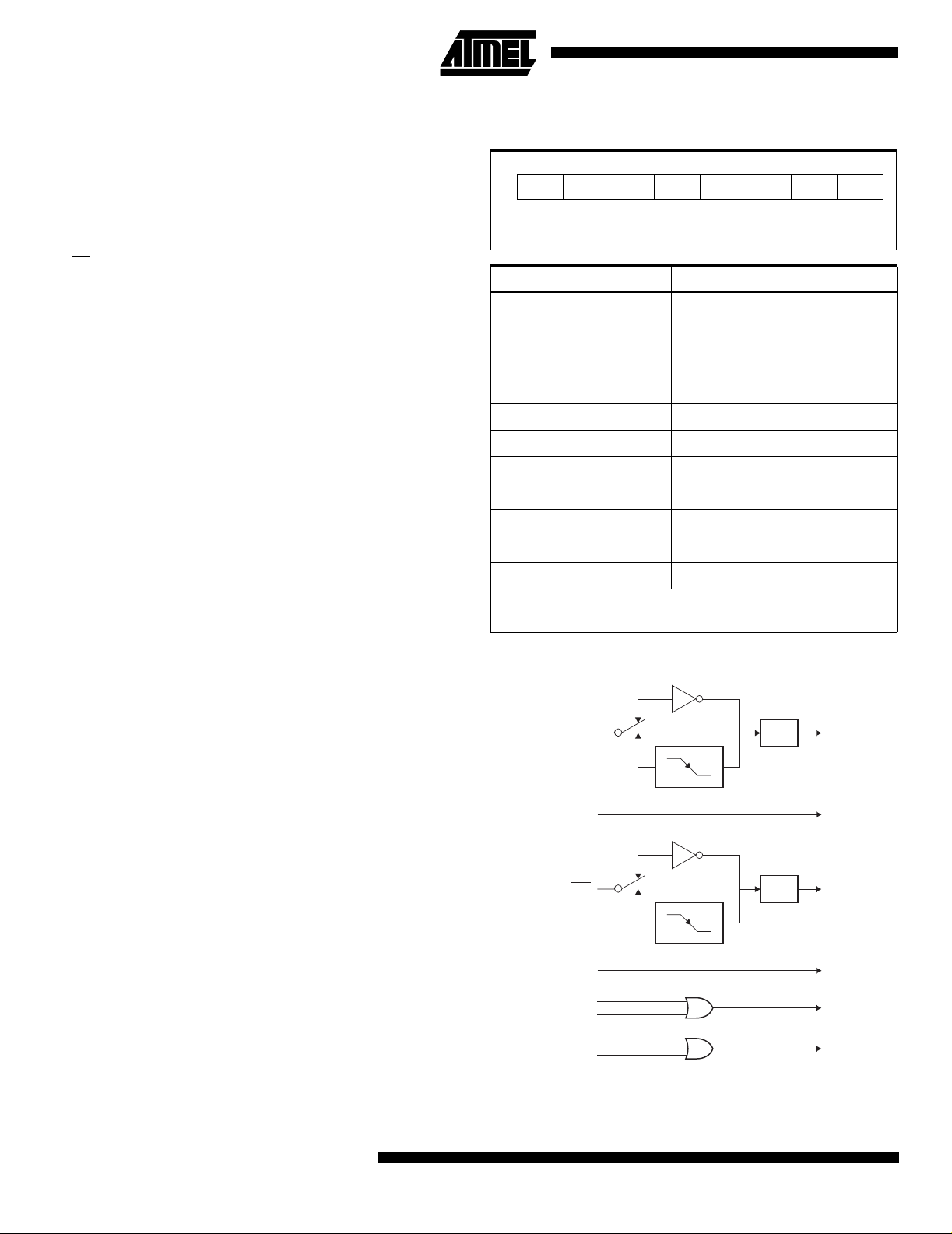
The values shown in this table are valid for TA = -40°C to 85°C and VCC = 4.0V to 5.5V, unless otherwise noted.
Symbol Parameter Condition Min Max Units
V
IL
V
IL1
V
IH
V
IH1
V
OL
V
OL1
V
OH
V
OH1
I
IL
I
TL
I
LI
RRST Reset Pulldown Resistor 10 30 KΩ
C
IO
I
CC
Notes: 1. Under steady state (non-transient) conditions, IOL must be externally limited as follows:
2. Minimum V
Input Low Voltage (Except EA)-0.50.2 V
Input Low Voltage (EA)-0.50.2 V
Input High Voltage (Except XTAL1, RST) 0.2 VCC+0.9 VCC+0.5 V
Input High Voltage (XTAL1, RST) 0.7 V
Output Low Voltage
Output Low Voltage
(Port 0, ALE, PSEN)
Output High Voltage
(Ports 1,2,3, ALE, PSEN
Output High Voltage
(Port 0 in External Bus Mode)
(1)
(Ports 1,2,3) IOL = 1.6 mA 0.45 V
(1)
)
= 3.2 mA 0.45 V
I
OL
I
= -60 µA, VCC = 5V ± 10% 2.4 V
OH
I
= -25 µA 0.75 V
OH
= -10 µA 0.9 V
I
OH
= -800 µA, VCC = 5V ± 10% 2.4 V
I
OH
I
= -300 µA 0.75 V
OH
= -80 µA 0.9 V
I
OH
Logical 0 Input Current (Ports 1,2,3) VIN = 0.45V -50 µA
Logical 1 to 0 Transition Current
(Ports 1,2,3)
V
= 2V, VCC = 5V ± 10% -650 µA
IN
Input Leakage Current (Port 0, EA) 0.45 < VIN < V
Pin Capacitance Test Freq. = 1 MHz, TA = 25°C 10 pF
Active Mode, 12 MHz 25 mA
Power Supply Current
Idle Mode, 12 MHz 6.5 mA
Power-down Mode
Maximum I
Maximum I
(1)
per port pin: 10 mA
OL
per 8-bit port:
OL
VCC = 5.5V 50 µA
Port 0: 26 mA Ports 1, 2, 3: 15 mA
Maximum total IOL for all output pins: 71 mA
exceeds the test condition, V
If I
OL
may exceed the related specification. Pins are not guaranteed to sink current greater
OL
than the listed test conditions.
for Power-down is 2V.
CC
*NOTICE: Stresses beyond those listed under “Absolute
Maximum Ratings” may cause permanent damage to the de vice. This is a stress ra ting only and
functional opera tion of the d ev ice at the se or an y
other conditions beyond those indicated in the
operational sections of this specification is not
implied. Exposure to absolute maximum rating
conditions for extended periods may affect
device reliability.
CC
CC
CC
CC
CC
CC
CC
CC
VCC+0.5 V
±10 µA
-0.1 V
-0.3 V
V
V
V
V
23
Page 24

AC Characteristics
Under operating conditions, load capacitance for Port 0, ALE/PROG, and PSEN = 100 pF; load capacitance for all other
outputs = 80 pF.
External Program and Data Memory Characteristics
12 MHz Oscillator Variable Oscillator
Symbol Parameter
1/t
t
LHLL
t
AVLL
t
LLAX
t
LLIV
t
LLPL
t
PLPH
t
PLIV
t
PXIX
t
PXIZ
t
PXAV
t
AVIV
t
PLAZ
t
RLRH
t
WLWH
t
RLDV
t
RHDX
t
RHDZ
t
LLDV
t
AVDV
t
LLWL
t
AVWL
t
QVWX
t
QVWH
t
WHQX
t
RLAZ
t
WHLH
CLCL
Oscillator Frequency 0 33 MHz
ALE Pulse Width 127 2t
Address Valid to ALE Low 43 t
Address Hold After ALE Low 48 t
ALE Low to Valid Instruction In 233 4t
ALE Low to PSEN Low 43 t
PSEN Pulse Width 205 3t
PSEN Low to Valid Instruction In 145 3t
Input Instruction Hold After PSEN 00ns
Input Instruction Float After PSEN 59 t
PSEN to Address Valid 75 t
Address to Valid Instruction In 312 5t
PSEN Low to Address Float 10 10 ns
RD Pulse Width 400 6t
WR Pulse Width 400 6t
RD Low to Valid Data In 252 5t
Data Hold After RD 00ns
Data Float After RD 97 2t
ALE Low to Valid Data In 517 8t
Address to Valid Data In 585 9t
ALE Low to RD or WR Low 200 300 3t
Address to RD or WR Low 203 4t
Data Valid to WR Transit ion 23 t
Data Valid to WR High 433 7t
Data Hold After WR 33 t
RD Low to Address Float 0 0 ns
RD or WR High to ALE High 43 123 t
-40 ns
CLCL
-25 ns
CLCL
-25 ns
CLCL
-65 ns
CLCL
-25 ns
CLCL
-45 ns
CLCL
-60 ns
CLCL
-25 ns
CLCL
-8 ns
CLCL
-80 ns
CLCL
-100 ns
CLCL
-100 ns
CLCL
-90 ns
CLCL
-28 ns
CLCL
-150 ns
CLCL
-165 ns
CLCL
-50 3t
CLCL
-75 ns
CLCL
-30 ns
CLCL
-130 ns
CLCL
-25 ns
CLCL
-25 t
CLCL
+50 ns
CLCL
+25 ns
CLCL
UnitsMin Max Min Max
24
AT89S52
Page 25

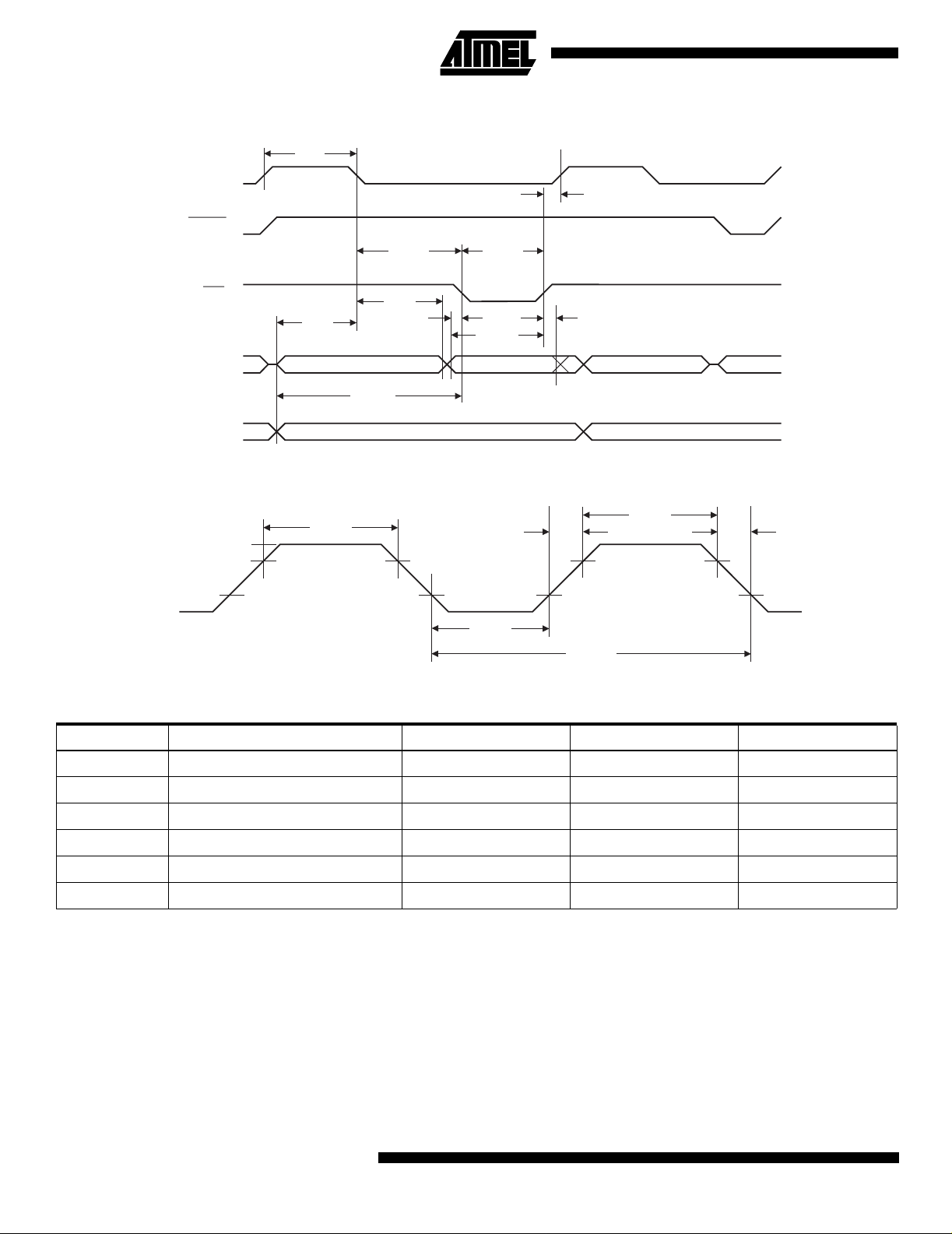
External Pro gr a m Memory Read Cycle
t
LHLL
ALE
t
AVLL
t
LLPL
PSEN
t
LLAX
PORT 0
A0 - A7 A0 - A7
t
AVIV
PORT 2
External Data Memory Read Cycle
t
LHLL
ALE
t
PLAZ
A8 - A15
t
LLIV
t
PLIV
t
PXIZ
t
PXIX
INSTR IN
t
PLPH
t
PXAV
t
AT89S52
A8 - A15
WHLH
PSEN
RD
PORT 0
PORT 2
t
LLDV
t
LLWL
t
LLAX
t
AVLL
A0 - A7 FROM RI OR DPL
t
AVWL
P2.0 - P2.7 OR A8 - A15 FROM DPH
t
AVDV
t
RLAZ
t
RLRH
t
RLDV
DATA IN INSTR IN
t
RHDZ
t
RHDX
A0 - A7 FROM PCL
A8 - A15 FROM PCH
25
Page 26
External Data Memory Write Cycle
t
LHLL
ALE
PSEN
t
LLWL
t
WLWH
t
WHLH
WR
PORT 0
PORT 2
t
AVLL
A0 - A7 FROM RI OR DPL
P2.0 - P2.7 OR A8 - A15 FROM DPH
t
AVWL
t
LLAX
t
QVWX
t
t
QVWH
DATA OUT INSTR IN
WHQX
A0 - A7 FROM PCL
A8 - A15 FROM PCH
External Clock Drive Waveforms
t
CHCX
t
CHCL
0.45V
V - 0.5V
CC
t
CHCX
0.7 V
CC
0.2 V - 0.1V
CC
t
CLCX
t
CLCH
t
CLCL
External Clock Drive
Symbol Parameter Min Max Units
26
1/t
t
CLCL
t
CHCX
t
CLCX
t
CLCH
t
CHCL
CLCL
Oscillator Frequency 0 33 MHz
Clock Period 30 ns
High Time 12 ns
Low Time 12 ns
Rise Time 5 ns
Fall Time 5 ns
AT89S52
Page 27

Serial Port Timing: Shift Register Mode Test Conditions
The values in this table are valid for V
Symbol Parameter
= 4.0V to 5.5V and Load Capacitance = 80 pF.
CC
12 MHz Osc Variable Oscillator
AT89S52
UnitsMin Max Min Max
t
XLXL
t
QVXH
t
XHQX
t
XHDX
t
XHDV
Serial Port Clock Cycle Tim e 1.0 12t
Output Data Setup to Clock Rising Edge 700 10t
Output Data Hold After Clock Rising Edge 50 2t
Input Data Hold After Clock Rising Edge 0 0 ns
Clock Rising Edge to Input Data Valid 700 10t
Shift Register Mode Timing Waveforms
INSTRUCTION
ALE
CLOCK
WRITE TO SBUF
OUTPUT DATA
CLEAR RI
INPUT DATA
AC Testing Input/Output Waveforms
0
t
QVXH
1
t
XHDV
2
t
XLXL
t
XHQX
0
VALID VALIDVALID VALIDVALID VALIDVALID VALID
1
(1)
3
t
2
XHDX
4
5
3
4
Float Waveforms
CLCL
-133 ns
CLCL
-80 ns
CLCL
-133 ns
CLCL
6
7
5
8
6
7
SET TI
SET RI
(1)
µs
V - 0.5V
CC
0.45V
0.2 V + 0.9V
CC
TEST POINTS
0.2 V - 0.1V
CC
Note: 1. AC Inputs dur ing testing are driven at VCC - 0.5V
for a logic 1 and 0.45V for a logic 0. Timing measurements are made at VIH min. for a lo gic 1 a nd VIL
max. for a logic 0.
V
LOAD
V
V
LOAD
LOAD
+ 0.1V
- 0.1V
Timing Reference
Points
- 0.1V
V
OL
+ 0.1V
V
OL
Note: 1. For timing purposes, a port pin is no longer floating
when a 100 mV change f r om lo ad voltage occurs. A
port pin begins to float w h en a 1 00 m V ch an ge f r om
the loaded V
OH/VOL
level occu rs .
27
Page 28

Orderi ng Information
Speed
(MHz)
24 4.0V to 5.5V AT89S52-24AC
33 4.5V to 5.5V AT89S52-33AC
= Preliminary Availability
Power
Supply Ordering Code Package Operation Range
AT89S52-24JC
AT89S52-24PC
AT89S52-24AI
AT89S52-24JI
AT89S52-24PI
AT89S52-33JC
AT89S52-33PC
44A
44J
40P6
44A
44J
40P6
44A
44J
40P6
Commercial
(0°C to 70°C)
Industrial
(-40°C to 85°C)
Commercial
(0°C to 70°C)
Package Type
44A 44-lead, Thin Plastic Gull Wing Quad Flatpack (TQFP)
44J 44-lead, Plastic J-leaded Chip Carrier (PLCC)
40P6 40-pin, 0.600" Wide, Plastic Dual Inline Package (PDIP)
28
AT89S52
Page 29

Pac ka ging Inf ormation
44A, 44-lead, Thin (1.0 mm) Plastic Gull Wing Quad
Flat Package (TQFP)
Dimensions in Millimeters and (Inches)*
0.80(0.031) BSC
0.20(.008)
0.09(.003)
PIN 1 ID
12.21(0.478)
11.75(0.458)
10.10(0.394)
9.90(0.386)
0
7
0.75(0.030)
0.45(0.018)
0.15(0.006)
0.05(0.002)
SQ
0.45(0.018)
0.30(0.012)
SQ
1.20(0.047) MAX
*Controlling dimension: millimeters
44J, 44-lead, Plastic J-leaded Chip Carrier (PLCC)
Dimensions in Inches and (Millimeters)
.045(1.14) X 45°
.032(.813)
.026(.660)
.050(1.27) TYP
PIN NO.1
IDENTIFY
.045(1.14) X 30° - 45°
.656(16.7)
SQ
.650(16.5)
.695(17.7)
.685(17.4)
.500(12.7) REF SQ
.022(.559) X 45° MAX (3X)
SQ
.012(.305)
.008(.203)
.630(16.0)
.590(15.0)
.021(.533)
.013(.330)
.043(1.09)
.020(.508)
.120(3.05)
.090(2.29)
.180(4.57)
.165(4.19)
40P6, 40-pin, 0.600" Wide, Plastic Dual Inline
Package (PDIP)
Dimensions in Inches and (Millimeters)
JEDEC STANDARD MS-011 AC
2.07(52.6)
.220(5.59)
SEATING
PLANE
MAX
.161(4.09)
.125(3.18)
.110(2.79)
.090(2.29)
.012(.305)
.008(.203)
2.04(51.8)
1.900(48.26) REF
.065(1.65)
.041(1.04)
.630(16.0)
.590(15.0)
.690(17.5)
.610(15.5)
PIN
1
.566(14.4)
.530(13.5)
.090(2.29)
.005(.127)
.065(1.65)
.015(.381)
.022(.559)
.014(.356)
0
REF
15
MAX
MIN
29
AT89S52
Page 30

Atmel Headquarters Atmel Product Operations
Corporate Headquarters
2325 Orchard Parkway
San Jose, CA 95131
TEL (408) 441-0311
FAX (408) 487-2600
Europe
Atmel SarL
Route des Arsenaux 41
Casa Postale 80
CH-1705 Fribourg
Switzerland
TEL (41) 26-426-5555
FAX (41) 26-426-5500
Asia
Atmel Asia, Ltd.
Room 1219
Chinachem Gol den P laza
77 Mody Road Tsimhatsui
East Kowloon
Hong Kong
TEL (852) 2721-9778
FAX (852) 2722-1369
Japan
Atmel Japan K.K.
9F, Tonetsu Shinkawa Bldg.
1-24-8 Shin kawa
Chuo-ku, Tokyo 104-0033
Japan
TEL (81) 3- 3523-3 551
FAX (81) 3-3523-7581
Atmel Colorado Springs
1150 E. Cheyenne Mtn. Blvd.
Colorado Springs, CO 80906
TEL (719) 57 6-330 0
FAX (719) 540-1759
Atmel Grenoble
Avenue de Rochepleine
BP 123
38521 Saint-Egreve Cedex, France
TEL (33) 4- 7658-3 000
FAX (33) 4-7658-3480
Atmel Heilbronn
Theresienstrasse 2
POB 3535
D-74025 Heilbronn, Germany
TEL (49) 71 31 67 25 94
FAX (49) 71 31 67 24 23
Atmel Nantes
La Chantrer ie
BP 70602
44306 Nantes Cedex 3, France
TEL (33) 0 2 40 18 18 18
FAX (33) 0 2 40 18 19 60
Atmel Rousset
Zone Industrielle
13106 Rousset Cedex, France
TEL (33) 4- 4253-6 000
FAX (33) 4-4253-6001
Atmel Smart Card ICs
Scottish Enterprise Technology Park
East Kilbride, Scotland G75 0QR
TEL (44) 1355-357-000
FAX (44) 1355-242-743
Fax-on-Demand
North America:
1-(800) 292-8635
International:
1-(408) 441-0732
e-mail
literature@atmel.com
Web Site
http://www.atmel.com
BBS
1-(408) 436-4309
© Atmel Corporation 2001.
Atmel Corporation makes no warranty for the use of its products, other than those expressly contained in the Company’s standard warranty
which is detailed in Atmel’s Terms and Conditions located on the Company’s web site. The Company assumes no responsibility for any errors
which may appear in this document, reserves the right to change devices or specifications detailed herein at any time without notice, and does
not make any commitment to update the information contained herein. No licenses to patents or other intellectual property of Atmel are granted
by the Company in connection with the sale of Atmel products, expressly or by implication. Atmel’s products are not authorized for use as critical
components in life support devices or systems.
ATMEL® is the registered trademark of A tmel.
MCS-51
trademarks of others.
®
is the registered trademark of Intel Corporation. Terms and product names in this document may be
Printed on recycled paper.
Rev.1919A-07/01/xM
 Loading...