

Page 1
Features
•
Compatible with MCS-51™ Products
•
4K Bytes of Reprogrammable Flash Memory
– Endurance: 1,000 Write/Erase Cycles
•
2.7V to 6V Operating Range
•
Fully Static Operation: 0 Hz to 12 MHz
•
Three-Level Program Memory Lock
•
128 x 8-Bit Internal RAM
•
32 Programmable I/O Lines
•
Two 16-Bit Timer/Counters
•
Six Interrupt Sources
•
Programmable Serial Channel
•
Low Power Idle and Power Down Modes
Description
The AT89LV51 is a low-voltage, high-performan ce CMOS 8-bit microcomputer with
4K bytes of Flash Programmable and Erasable Read Only Memory. The device is
manufactured us ing Atmel ’s high dens ity nonv olatil e memory te chnolo gy and is com patible with the industry standard MCS-51™ instruction set and p inout. The on-chip
Flash allows the program memory to be reprogrammed in-system or by a conventional nonvolatile memory programmer. By combining a versatile 8-bit CPU with Flash
on a monolithic chip, the Atmel AT89LV51 is a powerful microcomputer which provides a highly flexible and cost effective solution to many embedded control applications. The AT89LV51 operates at 2.7 volts up to 6.0 volts.
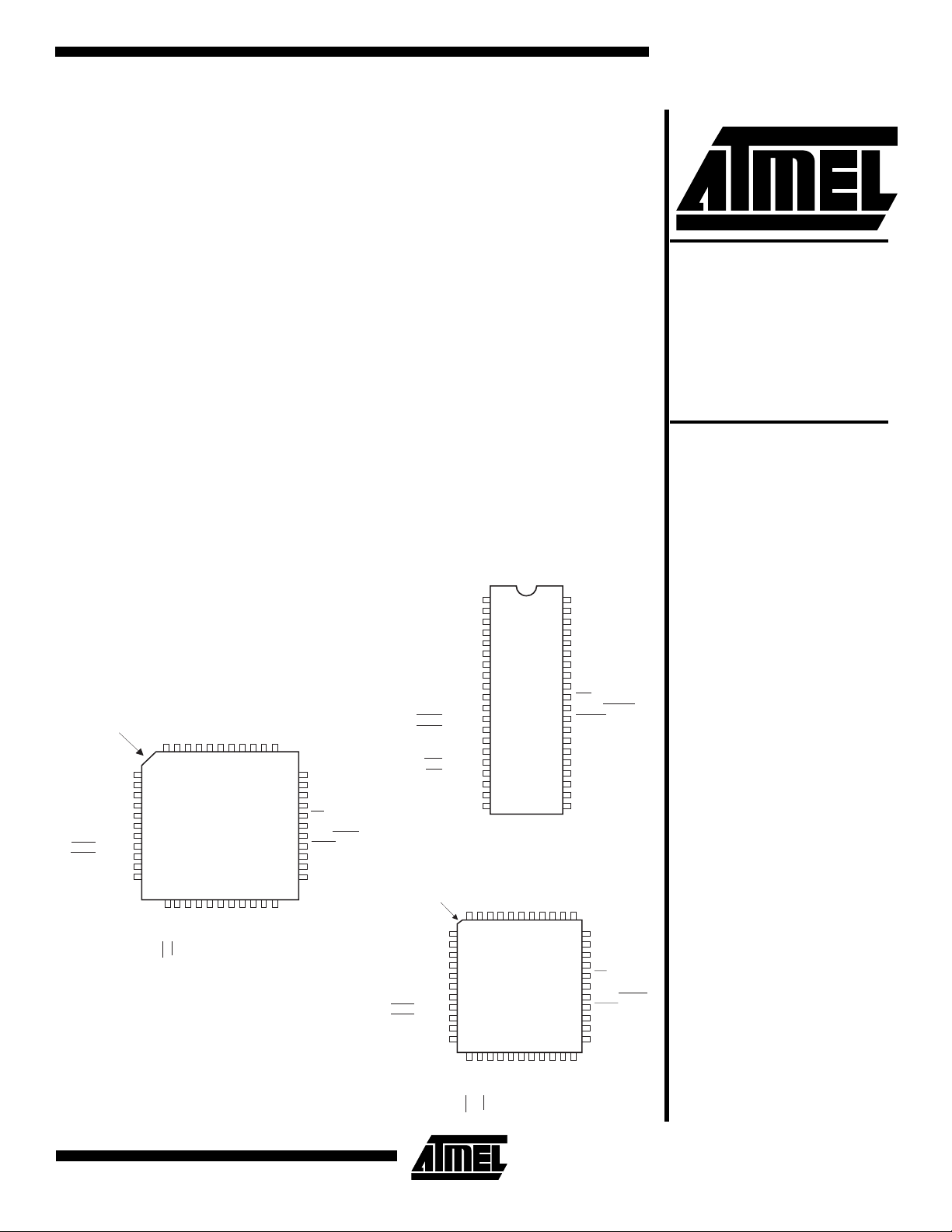
PDIP
(continued)
Pin Configurations
INDEX
CORNER
P1.5
P1.6
P1.7
RST
(RXD) P3.0
(TXD) P3.1
()P3.2INT0
()P3.3INT1
(T0) P3.4
(T1) P3.5
NC
P1.0
1
P1.1
2
P1.2
3
P1.3
4
P1.4
5
P1.5
6
7
TQFP
P1.3
P1.2
424340
41
15
14
XTAL2
()P3.7RD
P1.0
P1.1
16
GND
XTAL1
39
17
NC
38
18
GND
VCC
37
19
(A8) P2.0
P0.1 (AD1)
P0.0 (AD0)
36
35
21
20
(A9) P2.1
(A10) P2.2
P0.2 (AD2)
P0.3 (AD3)
34
33
32
31
30
29
28
27
26
25
24
23
22
(A11) P2.3
(A12) P2.4
P0.4 (AD4)
P0.5 (AD5)
P0.6 (AD6)
P0.7 (AD7)
EA/VPP
NC
ALE/PROG
PSEN
P2.7 (A15)
P2.6 (A14)
P2.5 (A13)
INDEX
CORNER
(RXD) P3.0
(TXD) P3.1
()P3.2INT0
()P3.3INT1
(T0) P3.4
(T1) P3.5
P1.4
44
1
2
3
4
5
6
7
8
9
10
11
13
12
()P3.6WR
P1.6
P1.7
8
RST
(RXD) P3.0
(TXD) P3.1
()P3.2INT0
()P3.3INT1
(T0) P3.4
(T1) P3.5
()P3.6WR
()P3.7RD P2.3 (A11)
XTAL2 P2.2 (A10)
XTAL1 P2.1 (A9)
9
10
11
12
13
14
15
16
17
18
19
GND P2.0 (A8)
20
PLCC
NC
P1.0
P1.1
P1.2
P1.4
P1.3
65444
2
1
P1.5
P1.6
P1.7
RST
NC
3
7
8
9
10
11
12
13
14
15
16
17 29
181920 24
()P3.6WR
()P3.7RD
21
XTAL2
22
XTAL1
23
GND
NC
40
39
38
37
36
35
34
33
32
31
30
29
28
27
26
25
24
23
22
21
VCC
P0.0 (AD0)
424340
252827
26
(A9) P2.1
(A8) P2.0
V
P0.0 (AD0)
P0.1 (AD1)
P0.2 (AD2)
P0.3 (AD3)
P0.4 (AD4)
P0.5 (AD5)
P0.6 (AD6)
P0.7 (AD7)
EA/VPP
ALE/PROG
PSEN
P2.7 (A15)
P2.6 (A14)
P2.5 (A13)
P2.4 (A12)
P0.2 (AD2)
P0.1 (AD1)
P0.3 (AD3)
41
39
38
37
36
35
34
33
32
31
30
(A10) P2.2
(A12) P2.4
(A11) P2.3
CC
P0.4 (AD4)
P0.5 (AD5)
P0.6 (AD6)
P0.7 (AD7)
EA/VPP
NC
ALE/PROG
PSEN
P2.7 (A15)
P2.6 (A14)
P2.5 (A13)
8-Bit
Microcontroller
with 4K Bytes
Flash
AT89LV51
0303D-D–12/97
4-45
Page 2
Block Diagram
4-46
AT89LV51
Page 3

AT89LV51
The AT89LV51 provides the following standard features:
4K bytes of Flash, 128 b ytes of RAM , 32 I/O lines, two 16bit timer/coun ters, a fiv e ve ctor two- leve l in terrupt arc hitec ture, a full duplex serial port, on-chip oscillator and clock
circuitry. In addition, the AT89LV51 is designed with static
logic for operation down to zero frequency an d supports
two software select able power saving mo des. The Idle
Mode stops the CPU while allowing the RAM,
timer/counters, serial port and interrupt system to continue
functioning. The Power Down Mode saves the RAM contents but freezes the os cillato r dis ablin g all othe r chip func tions until the next hardware reset.
Pin Description
V
CC
Supply voltage.
GND
Ground.
Port 0
Port 0 is an 8-bit open drain bidirectional I/O port. As an
output port each pin can sink eight TTL inputs. When 1s
are written to port 0 pins, the pins can be used as highimpedance inputs.
Port 0 may also be configured to be the multiplexed loworder address/data bus during accesses to ex ternal program and data memory . In this m ode P0 ha s int ernal pullups.
Port 0 also rece ives th e code by tes dur ing Fla sh prog ramming, and outputs the code bytes during program verification. External pu llups are requ ired dur ing pro gram ver ification.
Port 1
Port 1 is an 8-bit bidire ction al I/O por t w ith inter nal pullu ps.
The Port 1 output buffers can sink/source four TTL inputs.
When 1s are written to Port 1 pins they are pulled high by
the internal pullups and can be used as inputs. As inputs ,
Port 1 pins that are externally being pulled low will source
current (I
Port 1 also receives the low-order address bytes during
Flash programming and verification.
Port 2
Port 2 is an 8-bit bidire ction al I/O por t w ith inter nal pullu ps.
The Port 2 output buffers can sink/source four TTL inputs.
When 1s are written to Port 2 pins they are pulled high by
the internal pullups and can be used as inputs. As inputs ,
Port 2 pins that are externally being pulled low will source
current (I
Port 2 emits the high-order address byte during fetches
from external program memory and during accesses to
external data memory that use 16-bit addre sses ( MOVX @
DPTR). In this ap plication it uses strong internal pull ups
) because of the internal pullups.
IL
) because of the internal pullups.
IL
when emitting 1s. During accesses to external data memory that use 8-bit addresses (MOVX @ RI), Port 2 emits the
contents of the P2 Special Function Register.
Port 2 also receives the high-order address bits and some
control signals during Flash programming and verification.
Port 3
Port 3 is an 8-bit bidirectional I/O port with interna l pullups.
The Port 3 output buffers can sink/source four TTL inputs.
When 1s are written to Port 3 pins they are pulled high by
the internal pullups and can be used as inputs. As inputs,
Port 3 pins that are externally being pulled low will source
current (I
) because of the pullups.
IL
Port 3 also serv es t he fun ctions of v arious spe cial f eatures
of the AT89LV51 as listed below:
Port Pin Alternate Functions
P3.0 RXD (serial input port)
P3.1 TXD (serial output port)
P3.2 INT0
P3.3 INT1 (external interrupt 1)
P3.4 T0 (timer 0 external input)
P3.5 T1 (timer 1 external input)
P3.6 WR
P3.7 RD
(external interrupt 0)
(external data memory write strobe)
(external data memory read strobe)
Port 3 also receives some control signals for Flash programming and verification.
RST
Reset input. A high on this pin for two machine cycles while
the oscillator is running resets the device.
ALE/PROG
Address Latch Enable output pulse for latching the low byte
of the address during accesses to external memory. This
pin is also the program pulse input (PROG
) during Flash
programming.
In normal operation ALE is emitted at a constant rate of 1/6
the oscillator fr equen cy, and ma y be us ed for ext ernal timing or clocking purposes. Note, however, that one ALE
pulse is skipped during each access to external Data Memory.
PSEN
Program Store Enable is the read strobe to external program memory.
When the AT89LV51 is executing code from external program memory, PSEN
cycle, except that two PSEN
is activated twice each machine
activations are skipped during
each access to external data memory.
4-47
Page 4

EA
/V
PP
External Access Enable. EA must be strapped to GND in
order to enable the device to fetch code from external program memory locations starting at 0000H up to FFFFH.
Note, however, that if lock bit 1 is programmed, EA
will be
internally latched on reset.
should be strapped to VCC for internal program execu-
EA
tions.
This pin also receives the 12-volt programming enable voltage (V
) during Flash programming, when 12-volt pro-
PP
gramming is selected.
XTAL1
Input to the inverting os cillator ampl ifier and input to the
internal clock operating circuit.
XTAL2
Output from the inverting oscillator amplifier.
Special Function Registers
A map of the on-chip memory area called the Special Function Register (SFR) space is shown in Table 1.
Note that not all of the addre sses are occupi ed, and unoccupied addresses may not be implemented on the chip.
Read accesses to these addresses will in general return
random data, and write accesses will have an indeterminate effect.
User software should not write 1s to these unlisted locations, since they may be used in future products to invoke
new features. In th at case, th e reset or inac tive valu es of
the new bits will always be 0.
Timer 0 and 1
Timer 0 and Timer 1 in the AT89LV51 operate the same
way as Timer 0 and Timer 1 in the AT89C51.
Table 1.
AT89LV51 SFR Map and Reset Values
0F8H 0FFH
0F0H B
00000000
0E8H 0EFH
0E0H ACC
0D8H 0DFH
0D0H PSW
0C8H T2CON
0C0H 0C7H
0B8H IP
0B0H P3
0A8H IE
0A0H P2
98H SCON
90H P1
88H TCON
80H P0
00000000
00000000
00000000
XX000000
11111111
0X000000
11111111
00000000
11111111
00000000
11111111
T2MOD
XXXXXX00
SBUF
XXXXXXXX
TMOD
00000000
SP
00000111
RCAP2L
00000000
TL0
00000000
DPL
00000000
RCAP2H
00000000
TL1
00000000
DPH
00000000
TL2
00000000
TH0
00000000
TH2
00000000
TH1
00000000
PCON
0XXX0000
0F7H
0E7H
0D7H
0CFH
0BFH
0B7H
0AFH
0A7H
9FH
97H
8FH
87H
4-48
AT89LV51
Page 5

AT89LV51
Oscillator Characteristics
XTAL1 and XTAL2 are the input and output, resp ectively,
of an inverting amplifier which can be configured for use as
an on-chip oscillator, as shown in Figure 1. Either a quartz
crystal or ceramic resonator may be used. To drive the
device from an external clock source, XTAL2 should be left
unconnected while XTAL1 is driven as shown in Figure 2.
There are no requirements on the duty cycle of the external
clock signal, since the input to the internal clocking circuitry
is through a divide-by-two flip-flop, but minimum and maximum voltage high and low time specifications must be
observed
Idle Mode
In idle mode, the CPU puts itself to sleep while all the onchip peripherals remain active. The mode is invoked by
software. The content of the on-chip RAM and all the special functions registers remain unchanged during this
mode. The idle mode can be terminated by any en abled
interrupt or by a hardware reset.
It should be noted t hat when id le is termi nated by a hardware reset, the devi ce normally r esumes prog ram execution, from where it le ft off, up t o tw o machi ne c ycles befo re
the internal reset algorithm takes control. On-chip hardware
inhibits access to internal RAM in this event, but access to
the port pins is not inhibited. To eliminate the possibility of
an unexpected write to a port pin when Idle is terminated by
reset, the instruction following the one that invokes Idle
should not be one t hat writes to a port pin or to external
memory.
Figure 1.
Note: C1, C2 = 30 pF ± 10 pF for Crystals
Figure 2.
Oscillator Connections
C2
C1
= 40 pF ± 10 pF for Ceramic Resonators
XTAL2
XTAL1
GND
External Clock Drive Configuration
NC
EXTERNAL
OSCILLATOR
SIGNAL
XTAL2
XTAL1
GND
Power Do wn Mode
In the power down mode the oscillator is stopped, and the
instruction t hat invo kes po wer down is th e last instru ction
executed. The on-chip RAM and Special Function Registers retain their values until the power d own m ode is ter minated. The only exit fr om power do wn is a hard ware reset .
Reset redefines the SFRs but does not change the on-c hip
RAM. The reset should not be activated before V
CC
is
restored to its normal operating level and must be held
active long enough to allow the oscillator to restart and stabilize.
Status of External Pins During Idle and Power Down Modes
Mode Program Memory ALE PSEN PORT0 PORT1 PORT2 PORT3
Idle Internal 1 1 Data Data Data Data
Idle External 1 1 Float Data Address Data
Po w er Down Internal 0 0 Data Data Data Data
Po w er Down External 0 0 Float Data Data Data
4-49
Page 6
Program Memory Lock Bits
On the chip are three lock bits which can be left unprogrammed (U) or can be programmed (P) to obtain the additional features listed in the table below:
(1)
Lock Bit Protection Modes
Program Lock Bits Protection Type
LB1 LB2 LB3
1 U U U No program lock features.
2 P U U MOVC instructions executed
from external program
memory are disabled from
fetching code bytes from
internal memory, EA is
sampled and latched on
reset, and further
programming of the Flash is
disabled.
3 P P U Same as mode 2, also verify
is disabled.
4 P P P Same as mode 3, also
external execution is
disabled.
Note: 1. The lock b its can only be er as ed wit h the C hip Eras e
operation.
When lock bit 1 is programmed, the logic level at the EA pin
is sampled and latched during rese t. If the device is powered up without a reset, the latch initi alizes to a random
value, and holds that value until reset is activated. It is necessary that the latched value of EA
be in agreement with
the current logic level at that pin in order for the devic e to
function properly.
Programming the Flash
The AT89LV51 is normally shipped with the on-chip Flash
memory array in the erased state (i.e. contents=FFH) and
ready to be programmed.
The respective top-side marking and device signature
codes are listed below:
VPP = 12V
Top-Side Mark AT89LV51
xxxx
yyww
Signature (030H) = 1EH
(031H) = 61H
(032H) = FFH
The AT89LV51 code memory array is programmed byteby-byte.
To program any non-blank by te in the on-chip
Flash Code Memory, the entire m emory must be era sed
using the Chip Erase Mode.
Programming Algorithm:
Before programming the
AT89LV51, the address, data and control signals should be
set up according to the Flash programming mode table and
Figure 3 and Figure 4. To program the AT89LV51, the following sequence should be followed:
1. Input the desired memory location on the address
lines.
2. Input the appropriate data byte on the data lines.
3. Activate the correct combination of control signals.
4. Raise EA
5. Pulse ALE/PROG
/VPP to 12V.
once to program a byte in the Flash
array or the lock bits. The byte-write cycle is self-timed
and typically takes no more than 1.5 ms. Repeat ste ps
1 through 5 changing the address and data for the
entire array or until the end of the object file is reached.
Polling:
Data
The AT89LV51 features Data
Polling to indicate the end of a write cycle. During a write cycle, an
attempted read of the last byte written will result in the complement of the written data on PO.7. O nce the write cycle
has been completed, true data is valid o n all outputs, and
the next cycle may begin . Data
Polling may begi n any ti me
after a write cycle has been initiated.
Ready/Busy
be monitored by the RDY /B SY
:
The progress of byte programming can also
output signal. P3. 4 is p ull ed
low after ALE goes high during programming to indicate
BUSY. P3.4 is pu lled high again when programming is
done to indicate READY.
Program Verify:
If lock bits LB1 and LB2 have not been
programmed, the programmed code data can be read back
via the address and data line s for verific ation . The lock bits
cannot be verified dire ctly. Verificati on of the lock bits is
achieved by observing that their features are enabled.
Chip Erase:
The entire Flash array and the lock bits are
erased electr ical ly by usi ng t he pr oper co mbin ation of con trol signals and by holding ALE/PROG
low for 10 ms. The
code array is written with all “ 1”s. The c hip eras e operati on
must be executed before the code memory can be re-programmed.
Reading the Signature Bytes:
The signature bytes are
read by the same procedure as a normal verification of
locations 030H and 031H, ex cept that P3.6 and P3 .7 need
to be pulled to a logic low. The values returned are:
(030H) = 1EH indicates manufactured by Atmel
(031H) = 61H indicates 89LV51
(032H) = FFH indicates 12V programming
4-50
AT89LV51
Page 7

AT89LV51
Programming Interface
Every code byte in the Flash array c an be written and the
entire array can be eras ed by us ing the app ropria te co mbi-
All major programmi ng ve ndors of fer worl dwide s upport fo r
the Atmel microcontroller series. Please contact your local
programming vendor for the appropriate software revision.
nation of control signals. The write operation cycle is selftimed and once initiated, will automatically time itself to
completion.
Flash Programming Modes
Mode RST PSEN ALE/PROG EA/V
PP
Write Code Data H L 12V L H H H
Read Code Data H L H H L L H H
Write Lock Bit - 1 H L 12V H H H H
Bit - 2 H L 12V H H L L
Bit - 3 H L 12V H L H L
Chip Erase H L 12V H L L L
(1)
P2.6 P2.7 P3.6 P3.7
Read Signature Byte H L H H L L L L
Note: 1. Chip Erase requires a 10-ms PROG pulse.
Figure 3.
Programming the Flash
+5V
Figure 4.
Verifying the Flash
AT89LV51
ADDR.
OOOOH/OFFFH
SEE FLASH
PROGRAMMING
MODES ABLE
3-12 MHz
T
A0 - A7
A8 - A11
V
P1
P2.0 - P2.3
P2.6
P2.7
P3.6
P3.7
XTAL2 EA
XTAL1
GND
CC
P0
ALE
RST
PSEN
PGM
DATA
PROG
V/V
IH PP
V
IH
CC
4-51
Page 8

Flash Programming and Verification Characteristics
TA = 0°C to 70°C, VCC = 5.0V ± 10%
Symbol Parameter Min Max Units
(1)
V
PP
(1)
I
PP
1/t
CLCL
t
AVGL
t
GHAX
t
DVGL
t
GHDX
t
EHSH
t
SHGL
(1)
t
GHSL
t
GLGH
t
AVQV
t
ELQV
t
EHQZ
t
GHBL
t
WC
Note: 1. Only used in 12-volt programming mode.
Programming Enable Voltage 11.5 12.5 V
Programming Enable Current 25
Oscillator Frequency 3 12 MHz
Address Setup to PROG Low 48t
Address Hold After PROG 48t
Data Setup to PROG Low 48t
Data Hold After PROG 48t
P2.7 (ENABLE) High to V
PP
48t
CLCL
CLCL
CLCL
CLCL
CLCL
VPP Setup to PROG Low 10
VPP Hold After PROG 10
PROG Width 1 110
Address to Data Valid 48t
ENABLE Low to Data Valid 48t
Data Float After ENABLE 048t
CLCL
CLCL
CLCL
PROG High to BUSY Low 1.0
Byte Write Cycle Time 2.0 ms
A
µ
s
µ
s
µ
s
µ
s
µ
4-52
AT89LV51
Page 9

AT89LV51
Flash Programming and Verification Waveforms (VPP = 12V)
P1.0 - P1.7
P2.0 - P2.3
PORT 0
ALE/PROG
EA/V
PP
P2.7
(ENABLE)
P3.4
(RDY/BSY)
t
AVGL
t
SHGL
PROGRAMMING
ADDRESS
DATA IN
V
t
EHSH
PP
t
DVGL
t
GLGH
t
GHBL
t
GHDX
t
t
ELQV
GHAX
t
GHSL
LOGIC 1
LOGIC 0
BUSY
t
WC
VERIFICATION
ADDRESS
t
AVQV
DATA OUT
READY
t
EHQZ
4-53
Page 10

Absolute Maximum Ratings*
Operating Temperature.................................. -55°C to +125°C
*NOTICE: Stresses beyond those listed under “Absolute
Maximum Ratings” may cause permanent dam-
Storage Temperature..................................... -65°C to +150°C
age to the dev ice . This is a s tress rating only an d
functional oper ation of the de vi ce at these or any
Voltage on Any Pin
with Respect to Ground.....................................-1.0V to +7.0V
other conditions beyond those indicated in the
operational sections of this specification is not
implied. Exposure to absolute maximum rating
Maximum Operating Voltage............................................. 6.6V
conditions f or e xtended periods ma y af fect de vice
reliability .
DC Output Current......................................................15.0 mA
DC Characteristics
TA = -40°C to 85°C, VCC = 2.7V to 6.0V (unless otherwise noted)
Symbol Parameter Condition Min Max Units
V
IL
V
IL1
V
IH
V
IH1
V
OL
V
OL1
V
OH
V
OH1
I
IL
I
TL
I
LI
RRST Reset Pulldown Resistor 50 300 K
C
IO
I
CC
Input Low V oltage (Except EA)-0.50.2 V
Input Low Voltage (EA)-0.50.2 V
Input High Voltage (Except XTAL1, RST) 0.2 VCC + 0.9 VCC + 0.5 V
Input High Voltage (XTAL1, RST) 0.7 V
Output Low Voltage
Output Low Voltage
(Port 0, ALE , PSEN)
Output High Voltage
(Ports 1,2,3, ALE, PSEN
Output High Voltage
(Port 0 in External Bus Mode)
Logical 0 Input Current
(Ports 1,2,3)
Logical 1 to 0 Transition Current (Ports
1,2,3)
Input Leakage Current
(Port 0, EA
Pin Capacitance Test Freq. = 1 MHz, TA = 25°C 10 pF
Power Supply Current Active Mode, 12 MHz, VCC = 6V/3V 20/5.5 mA
Power Down Mode
)
(1)
(Ports 1,2,3) IOL = 1.6 mA 0.45 V
(1)
)
(2)
I
= 3.2 mA 0.45 V
OL
I
= -60 µA, VCC = 5V ± 10% 2.4 V
OH
I
= -20 µA 0.75 V
OH
I
= -10 µA0.9 VCCV
OH
IOH = -800 µA, VCC = 5V ± 10% 2.4 V
I
= -300 µA 0.75 V
OH
I
= -80 µA0.9 VCCV
OH
VIN = 0.45V -50
VIN = 2V -650
0.45 < V
Idle Mode, 12 MHz, V
VCC = 6V 100
V
CC
< V
IN
CC
= 6V/3V 5/1 mA
CC
= 3V 20
CC
CC
CC
- 0.1 V
CC
- 0.3 V
CC
VCC + 0.5 V
±
10
V
V
µ
A
µ
A
µ
A
Ω
µ
A
µ
A
Notes: 1. Under steady state (non-transient) conditions, IOL
must be externally limited as follows:
Maximum IOL per port pin: 10 mA
Maximum I
per 8-bit port:
OL
Port 0: 26 mA
Ports 1, 2, 3: 15 mA
4-54
AT89LV51
Maximum total IOL for all output pins: 71mA
If I
exceeds the test condition, VOL may exceed the
OL
related specification. Pins are not guaranteed to sink
current greater than the listed test conditions.
2. Minimum VCC for Power Down is 2V.
Page 11

AT89LV51
AC Characteristics
Under operating conditions, load capacitance for Port 0, ALE/PROG, and PSEN = 100 pF; load capacitance for all other
outputs = 80 pF.
External Program and Data Memory Characteristics
Symbol Parameter 12 MHz Oscillator Variable Oscillator Units
Min Max Min Max
1/t
CLCL
t
LHLL
t
AVLL
t
LLAX
t
LLIV
t
LLPL
t
PLPH
t
PLIV
t
PXIX
t
PXIZ
t
PXAV
t
AVIV
t
PLAZ
t
RLRH
t
WLWH
t
RLDV
t
RHDX
t
RHDZ
t
LLDV
t
AVDV
t
LLWL
t
AVWL
t
QVWX
t
QVWH
t
WHQX
t
RLAZ
t
WHLH
Oscillator Frequency 0 12 MHz
ALE Pulse Width 127 2t
Address Valid to ALE Low 4 3 t
Address Hold After ALE Low 48 t
ALE Low to Va lid Instruction In 233 4t
ALE Low to PSEN Low 43 t
PSEN Pulse Width 205 3t
PSEN Low to Valid Instruction In 145 3t
-40 ns
CLCL
-40 ns
CLCL
-35 ns
CLCL
-100 ns
CLCL
-40 ns
CLCL
-45 ns
CLCL
-105 ns
CLCL
Input Instruction Hold After PSEN 00ns
Input Instruction Float After PSEN 59 t
PSEN to Address Valid 75 t
-8 ns
CLCL
Address to Valid Instruction In 312 5t
-25 ns
CLCL
-105 ns
CLCL
PSEN Low to Address Float 10 10 ns
RD Pulse Width 400 6t
WR Pulse Width 400 6t
RD Low to Valid Data In 252 5t
-100 ns
CLCL
-100 ns
CLCL
-165 ns
CLCL
Data Hold After RD 00ns
Data Float After RD 97 2t
ALE Low to Valid Data In 517 8t
Address to Valid Data In 585 9t
ALE Low to RD or WR Low 200 300 3t
Address to RD or WR Low 203 4t
Data Valid to WR Transition 23 t
Data Valid to WR High 433 7t
Data Hold After WR 33 t
-50 3t
CLCL
-130 ns
CLCL
-60 ns
CLCL
-150 ns
CLCL
-50 ns
CLCL
-70 ns
CLCL
-150 ns
CLCL
-165 ns
CLCL
+50 ns
CLCL
RD Low to Address Float 0 0 ns
RD or WR High to ALE High 43 123 t
-40 t
CLCL
+40 ns
CLCL
4-55
Page 12

External Program Memory Read Cycle
t
LHLL
ALE
t
AVLL
t
LLPL
PSEN
t
LLAX
PORT 0
PORT 2
A0 - A7 A0 - A7
t
AVIV
A8 - A15
External Data Memory Read Cycle
t
LHLL
ALE
t
PLAZ
t
LLIV
t
PLIV
t
PXIZ
t
PXIX
INSTR IN
t
PLPH
t
PXAV
t
WHLH
A8 - A15
PSEN
RD
PORT 0
PORT 2
t
LLDV
t
LLWL
t
LLAX
t
AVLL
A0 - A7 FROM RI OR DPL
t
AVWL
P2.0 - P2.7 OR A8 - A15 FROM DPH
t
AVDV
t
RLAZ
t
RLRH
t
RLDV
DATA IN INSTR IN
t
RHDZ
t
RHDX
A0 - A7 FROM PCL
A8 - A15 FROM PCH
4-56
AT89LV51
Page 13

External Data Memory Write Cycle
t
LHLL
ALE
PSEN
t
LLWL
t
WLWH
t
WHLH
AT89LV51
WR
PORT 0
PORT 2
t
AVLL
A0 - A7 FROM RI OR DPL
P2.0 - P2.7 OR A8 - A15 FROM DPH
t
AVWL
t
LLAX
t
QVWX
External Clock Drive Waveforms
t
0.7 V
CC
CHCX
CC
0.45V
V - 0.5V
CC
0.2 V - 0.1V
t
t
QVWH
DATA OUT INSTR IN
t
CLCH
t
CLCX
WHQX
A0 - A7 FROM PCL
A8 - A15 FROM PCH
t
CHCX
t
CLCL
t
CHCL
External Clock Drive
Symbol Parameter Min Max Units
1/t
CLCL
t
CLCL
t
CHCX
t
CLCX
t
CLCH
t
CHCL
Oscillator Frequency 0 12 MHz
Clock Period 83.3 ns
High Time 20 ns
Low Time 20 ns
Rise Time 20 ns
Fall Tim e 20 ns
4-57
Page 14

Serial Port Timing: Shift Register Mode Test Conditions
V
LOAD
+ 0.1V
Timing Reference
Points
V
LOAD
- 0.1V
LOAD
V
V
OL
+ 0.1V
V
OL
- 0.1V
(VCC = 2.7V to 6V; Load Capacitance = 80 pF)
Symbol Parameter 12 MHz Osc Variable Oscillator Units
Min Max Min Max
t
XLXL
t
QVXH
t
XHQX
t
XHDX
t
XHDV
Serial Port Clock Cycle Time 1.0 12t
Output Data Setup to Clock Rising Edge 700 10t
Output Data Hold After Clock Rising Edge 50 2t
Input Data Hold After Clock Rising Edge 0 0 ns
Clock Rising Edge to Input Data Valid 700 10t
CLCL
-133 ns
CLCL
-117 ns
CLCL
-133 ns
CLCL
Shift Register Mode Timing Waveforms
s
µ
INSTRUCTION
0
1
2
ALE
t
XLXL
CLOCK
t
WRITE TO SBUF
OUTPUT DATA
CLEAR RI
QVXH
0
t
XHDV
VALID VALIDVALID VALIDVALID VALIDVALID VALID
t
INPUT DATA
AC Testing Input/Output Waveforms
V - 0.5V
CC
0.45V
0.2 V + 0.9V
CC
TEST POINTS
0.2 V - 0.1V
CC
XHQX
1
(1)
3
2
t
XHDX
4
5
3
Float Waveforms
6
4
5
7
6
8
7
SET TI
SET RI
(1)
Note: 1. AC inputs during testing are driven at 2.4V for a
logic “1” and 0.45V for a logic “0”. Timing measurements are made at 2.0 V f or a log ic “1” and 0.8V fo r a
logic “0”.
4-58
AT89LV51
Note: 1. For timing purposes, a port pin is no longer floating
when a 100 mV change fro m lo ad voltage occu rs. A
port pin begins to float w h en a 100 mV change from
the loaded V
OH/VOL
level occurs.
Page 15

ICC (mA)
24
20
16
AT89LV51
TYPICAL ICC (ACTIVE) at 25 C
o
AT89LV51
VCC = 6.0 V
12
8
4
0
0 4 8 12162024
VCC = 5.0 V
VCC = 3.0 V
F (MHz)
AT89LV51
ICC (mA)
4.8
4.0
3.2
2.4
1.6
0.8
0.0
0 4 8 12162024
TYPICAL ICC (IDLE) at 25 C
F (MHz)
o
VCC = 6.0 V
VCC = 5.0 V
VCC = 3.0 V
TYPICAL ICC vs.VOLTAGE- POWER DOWN (85°C)
20
I
15
C
C
10
µ
5
A
0
3.0V 4.0V 5.0V 6.0V
Notes: 1. XTAL1 tied to GND for Icc (power down)
2. Lock bits programmed
AT89LV51
Vcc VOLTAGE
4-59
Page 16

Ordering Information
Speed
(MHz) Power Supply Ordering Code Package Operation Range
12 2.7V to 6V AT89LV51-12AC
AT89LV51-12JC
AT89LV51-12PC
12 2.7V to 6V AT89LV51-12AI
AT89LV51-12JI
AT89LV51-12PI
44A
44J
40P6
44A
44J
40P6
Commercial
(0°C to 70°C)
Industrial
(-40°C to 85°C)
Package Type
44A 44 Lead, Thin Plastic Gull Wing Quad Flatpack (TQFP)
44J 44 Lead, Plastic J-Leaded Chip Carrier (PLCC)
40P6 40 Lead, 0.600" Wide, Plastic Dull Inline Package (PDIP)
4-60
AT89LV51
 Loading...