

Page 1

Features
•
Compatible with MCS-51™ Products
•
12K Bytes of In-System Reprogrammable Downloadable Flash Memory
- SPI Serial Interface for Program Downloading
- Endurance: 1,000 Write/Erase Cycles
•
2.7V to 6V Operating Range
•
Fully Static Operation: 0 Hz to 12 MHz
•
Three-Level Program Memory Lock
•
256 x 8 bit Internal RAM
•
32 Programmable I/O Lines
•
Three 16-bit Timer/Counters
•
Nine Interrupt Sources
•
Programmable UART Serial Channel
•
SPI Serial Interface
•
Low Power Idle and Power Down Modes
•
Interrupt Recovery From Power Down
•
Programmable Watchdog Timer
•
Dual Data Pointer
•
Power Off Flag
AT89LS53
8-Bit
Microcontroller
with 12K Bytes
Flash
Description
The AT89LS53 is a low-power, wide-voltage range, high-performance CMOS 8-bit
microcomputer with 12K bytes of downloadable Flash programmable and erasable
read only memory. The devic e i s manufa ctu r ed usin g Atmel’s high density nonvola til e
memory technol ogy and i s compa tible with the industr y stand ard 80C 51 ins truction
set and pinout. The on-chip downloadable Flash allows the program memory to be
reprogrammed in-syste m throug h an SPI seri al interfac e or by a conv ention al nonvol atile memory programmer. By combining a versatile 8-bit CPU with downloadable
Flash on a monolithic chip, the Atmel AT89LS53 is a powerful microcomputer which
provides a highly flex ible and co st effe ctive solu tion to many embedd ed con trol app lications.
The AT89LS53 provides the following standard features: 12K bytes of downloadable
Flash, 256 bytes of RAM, 32 I/O lines, programmable watchdog timer, two Data Pointers, three 16-bit timer/co unters, a six-ve ctor two-level inter rupt architecture, a ful l
duplex serial po rt, on-c hip osci llator, a nd clock circuitr y. In add ition, t he AT89L S53 is
designed with static logic for operation down to zero frequency and supports two software selectable power sa ving modes. The Id le Mode stops the CPU while allowing
the RAM, timer/counters, serial port, and interrupt system to continue functioning. The
Power Down Mode saves the RAM contents but freezes the osc illator, disabl ing all
other chip functions until the next interrupt or hardware reset.
The downloadable Flash can be changed a single byte at a time and is accessible
through the SPI serial interface. Holding RESET active forces the SPI bus into a serial
programming interface and allows the program memory to be written to or read from
unless Lock Bit 2 has been activated.
AT89LS53
0851B-B–12/97
4-249
Page 2
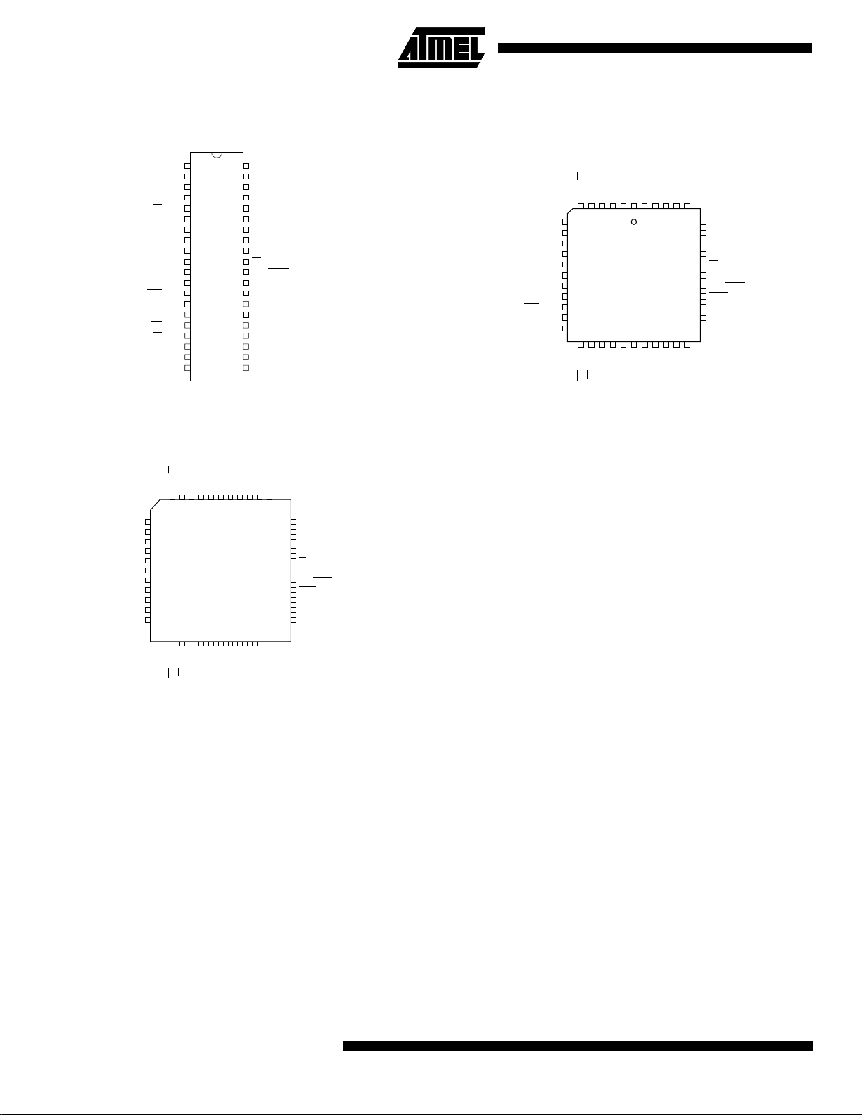
Pin Configurations
PDIP
1
(T2) P1.0
2
3
P1.2
4
P1.3
5
6
7
8
9
RST
10
11
12
13
14
(T0) P3.4
15
(T1) P3.5
16
17
18
XTAL2
19
XTAL1
20
GND
TQFP
P1.4 (SS)
P1.3
P1.2
P1.1 (T2 EX)
P1.0 (T2)NCVCC
4443424140393837363534
1
2
3
4
5
6
7
8
9
10
11
1213141516171819202122
(MOSI) P1.5
(MISO) P1.6
(SCK) P1.7
RST
(RXD) P3.0
(TXD) P3.1
(INT0) P3.2
(INT1) P3.3
(T0) P3.4
(T1) P3.5
(T2 EX) P1.1
(SS) P1.4
(MOSI) P1.5
(MISO) P1.6
(SCK) P1.7
(RXD) P3.0
(TXD) P3.1
(INT0) P3.2
(INT1) P3.3
(WR) P3.6
(RD) P3.7
NC
40
39
38
37
36
35
34
33
32
31
30
29
28
27
26
25
24
23
22
21
P0.0 (AD0)
VCC
P0.0 (AD0)
P0.1 (AD1)
P0.2 (AD2)
P0.3 (AD3)
P0.4 (AD4)
P0.5 (AD5)
P0.6 (AD6)
P0.7 (AD7)
EA/VPP
ALE/PROG
PSEN
P2.7 (A15)
P2.6 (A14)
P2.5 (A13)
P2.4 (A12)
P2.3 (A11)
P2.2 (A10)
P2.1 (A9)
P2.0 (A8)
P0.1 (AD1)
P0.2 (AD2)
P0.3 (AD3)
33
32
31
30
29
28
27
26
25
24
23
P0.4 (AD4)
P0.5 (AD5)
P0.6 (AD6)
P0.7 (AD7)
EA/VPP
NC
ALE/PROG
PSEN
P2.7 (A15)
P2.6 (A14)
P2.5 (A13)
(MOSI) P1.5
(MISO) P1.6
(SCK) P1.7
RST
(RXD) P3.0
(TXD) P3.1
(INT0) P3.2
(INT1) P3.3
(T0) P3.4
(T1) P3.5
PLCC
P1.4 (SS)
P1.3
P1.2
P1.1 (T2 EX)
65432
7
8
9
10
11
12
NC
13
14
15
16
17
1819202122232425262728
XTAL2
XTAL1
(RD) P3.7
(WR) P3.6
P1.0 (T2)NCVCC
1
4443424140
NC
GND
(A8) P2.0
P0.0 (AD0)
P0.1 (AD1)
P0.2 (AD2)
(A9) P2.1
(A10) P2.2
(A11) P2.3
P0.3 (AD3)
39
P0.4 (AD4)
38
P0.5 (AD5)
37
P0.6 (AD6)
36
P0.7 (AD7)
35
EA/VPP
34
NC
33
ALE/PROG
32
PSEN
31
P2.7 (A15)
30
P2.6 (A14)
29
P2.5 (A13)
(A12) P2.4
GND
GND
XTAL2
XTAL1
(A8) P2.0
(RD) P3.7
(WR) P3.6
(A9) P2.1
(A10) P2.2
(A11) P2.3
(A12) P2.4
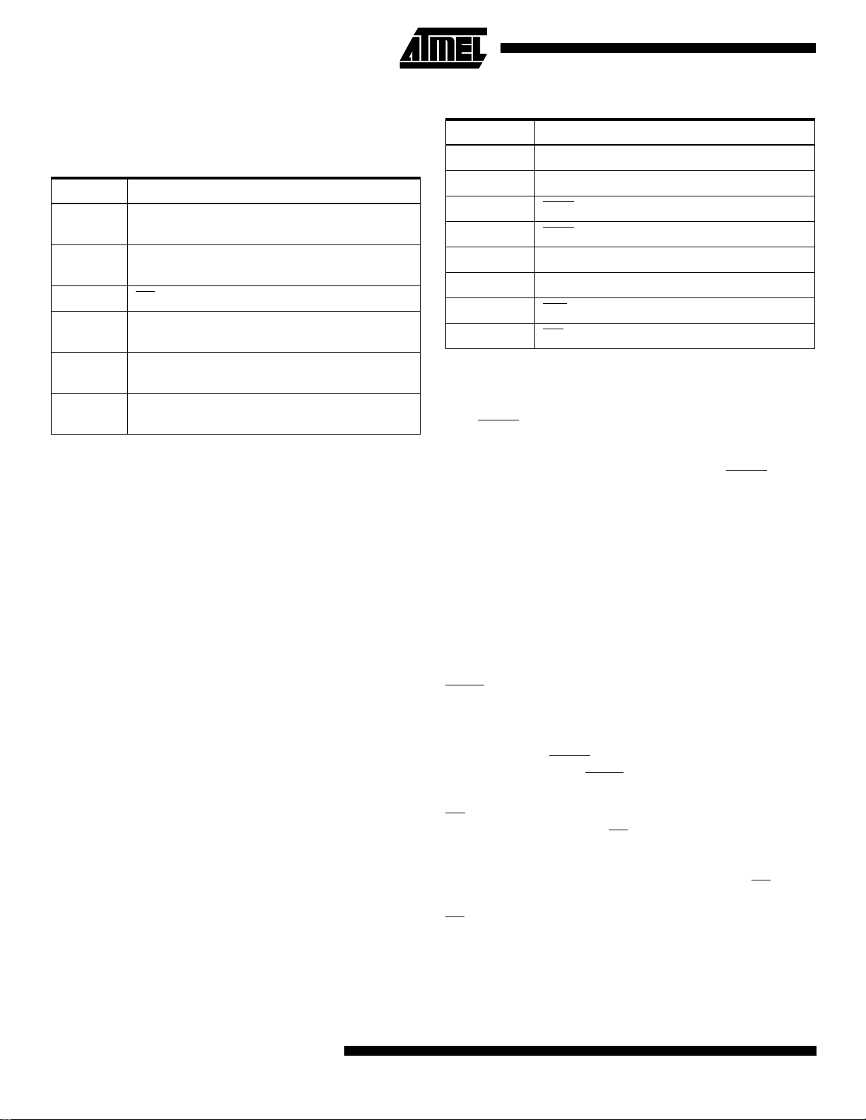
Pin Description
V
CC
Supply voltage.
GND
Ground.
Port 0
Port 0 is an 8-bit open drain bidirectional I/O port. As an
output port, each pin can sink eight TTL inputs. When 1s
are written to port 0 pins, the pins can be used as highimpedance inputs.
Port 0 can also be configu red to be the multiplex ed loworder address/data bus during accesses to ex ternal program and data memory. In this mode, P0 has internal pullups.
4-250
AT89LS53
Port 0 also receives the code bytes during Flash programming and outputs the code bytes durin g program verifica tion. External pullu ps are require d duri ng prog ram ve rifica tion.
Port 1
Port 1 is an 8-bit bidirectional I/O port with interna l pullups.
The Port 1 output buffers can sink/source four TTL inputs.
When 1s are writte n to Po rt 1 pi ns, they a re pul led high by
the internal pullups and can be used as inputs. As inputs,
Port 1 pins that are externally being pulled low will source
current (I
) because of the internal pullups.
IL
Some Port 1 pins p rovide additi onal functions. P1.0 and
P1.1 can be config ured to be th e timer/count er 2 ext ernal
count input (P1.0/T2) and the timer/counter 2 trigger input
(P1.1/T2EX), respectively.
Page 3
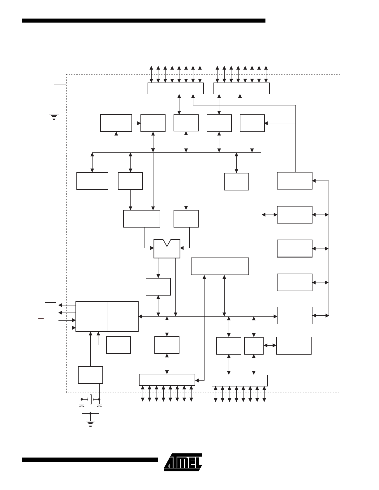
Block Diagram
AT89LS53
V
CC
GND
B
REGISTER
RAM ADDR.
REGISTER
P0.0 - P0.7
PORT 0 DRIVERS
RAM
ACC
TMP2 TMP1
PORT 0
LATCH
P2.0 - P2.7
PORT 2 DRIVERS
PORT 2
LATCH
STACK
POINTER
FLASH
PROGRAM
ADDRESS
REGISTER
BUFFER
PSEN
ALE/PROG
EA / V
RST
PC
ALU
INTERRUPT, SERIAL PORT,
AND TIMER BLOCKS
PSW
TIMING
AND
PP
CONTROL
OSC
INSTRUCTION
REGISTER
WATCH
DOG
PORT 3
LATCH
PORT 3 DRIVERS
P3.0 - P3.7
PORT 1
LATCH
PORT 1 DRIVERS
P1.0 - P1.7
SPI
PORT
INCREMENTER
PROGRAM
COUNTER
DPTR
PROGRAM
LOGIC
4-251
Page 4
Pin Description
Furthermore, P1.4, P1.5, P1.6, and P1.7 can be configured
as the SPI slave port select, data input/output and shift
clock input/output pins as shown in the following table.
Port Pin Alternate Functions
P1.0
P1.1
P1.4 SS
P1.5
T2 (external count input to Timer/Counter
2), clock-out
T2EX (Timer/Counter 2 capture/reload
trigger and direction control)
(Slave port select input)
MOSI (Master data output, slave data input
pin for SPI channel)
Port Pin Alternate Functions
P3.0 RXD (serial input port)
P3.1 TXD (serial output port)
P3.2 INT0
P3.3 INT1
P3.4 T0 (timer 0 external input)
P3.5 T1 (timer 1 external input)
P3.6 WR
P3.7 RD
(external interrupt 0)
(external interrupt 1)
(external data memory write strobe)
(external data memory read strobe)
P1.6
P1.7
Port 1 also receives the low-order address bytes during
Flash programming and verification.
Port 2
Port 2 is an 8-bit bidire ction al I/O por t w ith inter nal pullu ps.
The Port 2 output buffers can sink/source four TTL inputs.
When 1s are written to Port 2 pins , they are p ulled hi gh by
the internal pullups and can be used as inputs. As inputs ,
Port 2 pins that are externally being pulled low will source
current (I
Port 2 emits the high-order address byte during fetches
from external program memory and during accesses to
external data memory that use 16-bit addre sses (MO VX @
DPTR). In this application, Port 2 uses strong internal pullups when emitting 1s. During accesses to external data
memory that use 8-bit addresses (MOVX @ RI), Port 2
emits the contents of the P2 Special Function Register.
Port 2 also receives the high-order address bits and some
control signals during Flash programming and verification.
Port 3
Port 3 is an 8 bit b idirec tional I/O port with i nternal pul lups.
The Port 3 output buffers can sink/source four TTL inputs.
When 1s are written to Port 3 pins , they are p ulled hi gh by
the internal pullups and can be used as inputs. As inputs ,
Port 3 pins that are externally being pulled low will source
current (I
Port 3 also se rves the fu nctio ns of vari ous sp ecial f eat ures
of the AT89LS53, as shown in the following table.
Port 3 also receives some control signals for Flash programming and verification.
MISO (Master data input, slave data output
pin for SPI channel)
SCK (Master clock output, slave clock input
pin for SPI channel)
) because of the internal pullups.
IL
) because of the pullups.
IL
RST
Reset input. A high on this pin for two machine cycles while
the oscillator is running resets the device.
ALE/PROG
Address Latch Enable is an output pulse for latching the
low byte of the address during accesses to external memory. This pin is also the program pulse input (PROG
Flash programming.
In normal operation, ALE is emitte d at a con stant rate of 1/
6 the oscillator frequency and may be used for external timing or clocking purposes. Note, however, that one ALE
pulse is skipped d ur in g ea ch ac c ess to ex ter na l d ata mem ory.
If desired, ALE operation can be disabled by setting bit 0 of
SFR location 8 EH. With the bit se t, ALE is activ e only du ring a MOVX or MOVC instruction. Otherwise, the pin is
weakly pulled high. Setting the ALE-disable bit has no
effect if the microcontroller is in external execution mode.
PSEN
Program Store Enable is the read strobe to external program memory.
When the AT89LS53 is executing code from external program memory, PSEN
cycle, except that two PSEN
each access to external data memory.
/V
EA
PP
External Access Enable. EA must be strapped to GN D in
order to enable the device to fetch code from external program memory locations starting at 0000H up to FFFFH.
Note, however, that if lock bit 1 is programmed, EA
internally latched on reset.
should be strapped to VCC for internal program execu-
EA
tions. This pin also recei ves the 12-volt programmi ng
enable voltage ( V
volt programming is selected.
is activated twice each machine
activations are skipped during
) during Flash prog ramming when 12-
PP
) during
will be
4-252
AT89LS53
Page 5

AT89LS53
XTAL1
Input to the inverting os cillator ampl ifier and input to the
internal clock operating circuit.
XTAL2
Output from the inverting oscillator amplifier.
Special Function Registers
A map of the on-chip memory area called the Special Function Register (SFR) space is shown in Table 1.
Note that not all of the address es are occupied, and unoccupied addresses may not be implemented on the chip.
Read accesses to these addresses will in general return
random data, and write accesses will have an indeterminate
effect.
Table 1.
0F8H 0FFH
0F0H
0E8H 0EFH
0E0H
0D8H 0DFH
0D0H
0C8H
AT89LS53 SFR Map and Reset Values
B
00000000
ACC
00000000
PSW
00000000
T2CON
00000000
T2MOD
XXXXXX00
RCAP2L
00000000
RCAP2H
00000000
TL2
00000000
SPCR
000001XX
TH2
00000000
0F7H
0E7H
0D7H
0CFH
0C0H 0C7H
0B8H
0B0H
0A8H
0A0H
98H
90H
88H
80H
IP
XX000000
P3
11111111
IE
0X000000
P2
11111111
SCON
00000000
P1
11111111
TCON
00000000
P0
11111111
SBUF
XXXXXXXX
TMOD
00000000
SP
00000111
SPSR
00XXXXXX
TL0
00000000
DP0L
00000000
TL1
00000000
DP0H
00000000
TH0
00000000
DP1L
00000000
TH1
00000000
DP1H
00000000
WCON
00000010
SPDR
XXXXXXXX
PCON
0XXX0000
0BFH
0B7H
0AFH
0A7H
9FH
97H
8FH
87H
4-253
Page 6

User software shou ld not write 1s to these unlisted locations, since they may be u sed in future products to invoke
new features. In that case, the reset or inactive values of the
new bits will always be 0.
Timer 2 Registers
registers T2CON (shown in Table 2) and T2MOD (shown in
Table 9) for Timer 2. The register pa ir (RC AP 2H, RCA P2 L)
are the Capture/Reload registers for Timer 2 in 16 bit capture mode or 16-bit auto-reload mode.
Watchdog Control Register
control bits for the Watchdog Timer (shown in Table 3). The
DPS bit selects one of two DPTR registers available.
Control and status b its ar e con tai ned in
The WCON register con tains
SPI Registers
eral Interface are contained in registers SPCR (shown in
Table 4) and SPSR (shown in Table 5). The SPI data bits
are contained in the SPDR register. Writing the SPI data
register during serial data transfer sets the Write Collision
bit, WCOL, in the SPSR register. The SPDR is double buffered for writing and the values in SPDR are not changed by
Reset.
Interrupt Registers
individual interrupt enable bits are in the IE register. In addition, the individual interrupt enable bit for the SPI is in the
SPCR register. Two priorities ca n be set for each of the si x
interrupt sources in the IP register.
Control and status bits for the Serial Periph-
The global interrupt enable bit and the
Table 2.
T2CON Address = 0C8H Reset Value = 0000 0000B
Bit Addressable
Symbol Function
TF2
EXF2
RCLK
TCLK
EXEN2
T2CON—Timer/Counter 2 Control Register
TF2 EXF2 RCLK TCLK EXEN2 TR2 C/T2
Bit76543210
Timer 2 overflow flag set by a Timer 2 overflow and must be cleared by software. TF2 will not be set when
either RCLK = 1 or TCLK = 1.
Timer 2 external flag set when either a capture or reload is caused by a negative transition on T2EX and
EXEN2 = 1. When Timer 2 interrupt is enabled, EXF2 = 1 will cause the CPU to vector to the Timer 2 interrupt
routine. EXF2 must be cleared by software. EXF2 does not cause an interrupt in up/down counter mode
(DCEN = 1).
Receive clock enable. When set, causes the serial port to use Timer 2 overflow pulses for its receive clock in
serial port Modes 1 and 3. RCLK = 0 causes Timer 1 overflows to be used for the receive clock.
Transmit clock enable. When set, causes the serial port to use Timer 2 overflow pulses for its transmit clock in
serial port Modes 1 and 3. TCLK = 0 causes Timer 1 overflows to be used for the transmit clock.
Timer 2 external enable. When set, allows a capture or reload to occur as a result of a negative transition on
T2EX if Timer 2 is not being used to clock the serial port. EXEN2 = 0 causes Timer 2 to ignore events at
T2EX.
CP/RL2
TR2 Start/Stop control for Timer 2. TR2 = 1 starts the timer.
C/T2
CP/RL2
4-254
Timer or counter select for Timer 2. C/T2 = 0 for timer function. C/T2 = 1 for external event counter (falling
edge triggered).
Capture/Reload select. CP/RL2 = 1 causes captures to occur on negative transitions at T2EX if EXEN2 = 1.
CP/RL2
when EXEN2 = 1. When either RCLK or TCLK = 1, this bit is ignored and the timer is forced to auto-reload on
Timer 2 overflow.
= 0 causes automatic reloads to occur when Timer 2 overflows or negative transitions occur at T2EX
AT89LS53
Page 7

AT89LS53
Dual Data Pointer Registers
nal data memory, two banks of 16 bit Data Pointer Regis ters are provided: DP0 at SFR address locations 82H-83H
and DP1 at 84H-85H. Bit DPS = 0 in SFR WCO N selec ts
DP0 and DPS = 1 selects DP1. The user should always initalize the DPS bit to the appropriate value before accessing
the respective Data Pointer register.
Table 3.
WCON Address = 96H Reset Value = 0000 0010B
Bit76543210
Symbol Function
PS2
PS1
PS0
DPS Data Pointer Register Select. DPS = 0 selects the first bank of Data Pointer Register, DP0, and DPS = 1
WCON—Watchdog Control Register
PS2 PS1 P S0 reserved reserved DPS WDTRST WDTEN
Prescaler Bits for the Watchdog Timer. When all three bits are set to “0”, the watchdog timer has a nominal
period of 16 ms. When all three bits are set to “1”, the nominal period is 2048 ms.
selects the second bank, DP1
To facilitate accessing exter-
Power Off Flag
bit_4 (PCON.4) in the PCON SFR. PO F is set to “ 1” durin g
power up. It can be set and reset under software control
and is not affected by RESET.
The Power Off Flag (POF) is located at
WDTRST Watchdog Timer Reset. Each time this bit is set to “1” by user software, a pulse is generated to reset the
watchdog timer. The WDTRST bit is then automatically reset to “0” in the next instruction cycle. The
WDTRST bit is Write-Only.
WDTEN Watchdog Timer Enable Bit. WDTEN = 1 enables the watchdog timer and WDTEN = 0 disables the
watchdog timer.
4-255
Page 8

Table 4
. SPCR—SPI Control Register
SPCR Address = D5H Reset V alue = 0000 01XXB
SPIE SPE DORD MSTR CPOL CPHA SPR1 SPR0
Bit76543210
Symbol Function
SPIE SPI Interrupt Enable. This bit, in conjunction with the ES bit in the IE register, enables SPI interrupts: SPIE
= 1 and ES = 1 enable SPI interrupts. SPIE = 0 disables SPI interrupts.
SPE SPI Enable. SPI = 1 enables the SPI channel and connects SS
P1.6, and P1.7. SPI = 0 disables the SPI channel.
DORD Data Order. DORD = 1 selects LSB first data transmission. DORD = 0 selects MSB first data transmission.
MSTR Master/Slave Select. MSTR = 1 selects Master SPI mode. MSTR = 0 selects Slave SPI mode.
CPOL Clock Polarity. When CPOL = 1, SCK is high when idle. When CPOL = 0, SCK of the master device is low
when not transmitting. Please refer to figure on SPI Clock Phase and Polarity Control.
CPHA Clock Phase. The CPHA bit together with the CPOL bit controls the clock and data relationship between
master and slave. Please refer to figure on SPI Clock Phase and Polarity Control.
SPR0
SPR1
Table 5.
SPSR Address = AAH Reset Value = 00XX XXXXB
SPI Clock Rate Select. These two bits control the SCK rate of the device configured as master. SPR1 and
SPR0 have no effect on the slave. The relationship between SCK and the oscillator frequency, F
follows:
SPR1 SPR0 SCK = F
00 4
01 16
10 64
11 128
SPSR—SPI Status Register
divided by
OSC.
, MOSI, MISO and SCK to pins P1.4, P1.5,
, is as
OSC.
SPIFWCOL——————
Bit76543210
Symbol Function
SPIF SPI Interrupt Flag. When a serial transfer is complete, the SPIF bit is set and an interrupt is generated if
SPIE = 1 and ES = 1. The SPIF bit is cleared by reading the SPI status register with SPIF and WCOL bits
set, and then accessing the SPI data register.
WCOL Write Collision Flag. The WCOL bit is set if the SPI data register is written during a data transfer. During
data transfer, the result of reading the SPDR register may be incorrect, and writing to it has no effect. The
WCOL bit (and the SPIF bit) are cleared by reading the SPI status register with SPIF and WCOL set, and
then accessing the SPI data register.
4-256
AT89LS53
Page 9

AT89LS53
Table 6.
SPDR Address = 86H Reset V alue = unchanged
Data Memory - RAM
The AT89LS53 implements 256 bytes of RAM. The upper
128 bytes of RAM occupy a parallel space to the Special
Function Registers. That means the upper 128 bytes have
the same addresses as the SFR sp ace but ar e physic ally
separate from SFR space.
When an instruction accesses an internal location above
address 7FH, the address mode used in the instruction
specifies whether the CPU accesses the upper 128 bytes
of RAM or the SFR space. Instructions that use direct
addressing access SFR space.
For example, the following direct addressing instruction
accesses the SFR at location 0A0H (which is P2).
Instructions that use indirect addressing access the upper
128 bytes of RAM. For example, the following indirect
addressing instru ct ion , where R0 contains 0A0H, acc es s es
the data byte at address 0A0H, rather than P2 (whose
address is 0A0H).
Note that stack operations are examples of indirect
addressing, so the upper 128 byte s of data RAM are avail able as stack space.
SPDR—SPI Data Register
SPD7 SPD6 SPD5 SPD4 SPD3 SPD2 SPD1 SPD0
Bit76543210
Programmable Watchdog Timer
The programmable Watchdog Timer (WDT) operates from
an independent oscillator. T he prescaler bits, PS0, PS1
and PS2 in SFR W CON are us ed to set th e period of the
Watchdog Timer from 16 ms to 2048 ms. The available
timer periods are shown in the following table and the
= 5V) are within ±30% of the
CC
Period (nominal)PS2 PS1 PS0
MOV 0A0H, #data
MOV @R0, #data
actual timer periods (at V
nominal.
The WDT is disabled by Power-on Reset and during Power
Down. It is enable d by setting the WDTE N bit in SFR
WCON (addres s = 96 H). The W DT is reset by setti ng the
WDTRST bit in WCO N. When the WDT times out without
being reset or disabled, an in terna l RST pu ls e is gene rated
to reset the CPU.
Table 7.
Watchdog Timer Period Selection
WDT Prescaler Bits
0 0 0 16 ms
0 0 1 32 ms
0 1 0 64 ms
0 1 1 128 ms
1 0 0 256 ms
1 0 1 512 ms
1 1 0 1024 ms
1 1 1 2048 ms
4-257
Page 10
Timer 0 and 1
Timer 0 and Timer 1 in the AT89LS53 operate the same
way as Timer 0 and Timer 1 in the AT89C51, AT89C52 and
AT89C55. For further information, see the October 1995
Microcontroller Data Book, page 2-4 5, section titled,
“Timer/Counters.”
Table 8.
Timer 2 Operating Modes
RCLK + TCLK CP/RL2
0 0 1 16-bit Auto-Reload
0 1 1 16-bit Capture
TR2 MODE
Timer 2
Timer 2 is a 16 bit Timer/Counter that can operate as either
a timer or an event counter. The type of operation is
selected by bit C/T2
Timer 2 has three operating modes: capture, auto-reload
(up or down counting), and baud rate generator. The
modes are selected by bits in T2CON, as shown in Table 8.
Timer 2 consists of two 8- bi t regi st er s, TH2 and TL2. I n the
Timer function, the TL2 r egister is incremented ever y
machine cycle. Since a machine cycle consists of 12 oscillator periods, the count rate is 1/12 of the oscillator frequency.
In the Counter function, the register is incremented in
response to a 1-to-0 transition at its corresponding external
input pin, T2. In thi s func tion, the extern al i nput is sa mpled
during S5P2 of every machin e cycle. When the samples
show a high in one cycle and a low in the next cycle, the
count is incremented. The new count value appears in the
register during S3P1 of the cycle following the one in which
the transition was detected. Since two machine cycles (24
oscillator periods ) ar e requi r ed to r ec og niz e a 1 -t o- 0 tran si tion, the maximum count rate is 1/24 of the oscillator frequency. To ensure that a gi ven level is sam pled at least
once before it changes, the level should be held for at least
one full machine cycle.
in the SFR T2 C ON (sh o w n i n Ta bl e 2).
1X1
Baud Rate
Generator
X X 0 (Off)
Capture Mode
In the capture mode, two options are selected by bit
EXEN2 in T2CON. If EXEN2 = 0, Timer 2 is a 16 bit timer
or counter which upon overflow sets bit TF2 in T2CON.
This bit can then be used to generate an interrupt. If
EXEN2 = 1, Timer 2 p er forms t he sa me operation, but a 1 to-0 transition at external input T2EX also causes the current value in TH2 and TL2 to be captured into RCAP2H and
RCAP2L, resp ective ly. In addi tion, th e transit ion at T2E X
causes bit EXF2 in T2CON to be set. The EXF2 bit, like
TF2, can generate an interrupt. The capture mode is illustrated in Figure 1.
Auto-Reload (Up or Down Counter)
Timer 2 can be programmed to count up or down when
configured in its 16 bit auto-reload mode. This feature is
invoked by the DCEN (Down Counter Enable) bit located in
the SFR T2MOD (see Table 9). Upon reset, the DCEN bit
is set to 0 so that ti mer 2 will defa ult to count u p. When
DCEN is set, Timer 2 can coun t up or down, depend ing on
the value of the T2EX pin.
Figure 1.
OSC
T2EX PIN
4-258
Timer 2 in Capture Mode
÷12
T2 PIN
TRANSITION
DETECTOR
AT89LS53
C/T2 = 0
C/T2 = 1
EXEN2
CONTROL
TR2
CAPTURE
CONTROL
TH2 TL2
RCAP2LRCAP2H
EXF2
TF2
OVERFLOW
TIMER 2
INTERRUPT
Page 11

AT89LS53
Figure 2 shows Timer 2 automaticall y counting up when
DCEN = 0. In this mod e, two options a re selecte d by bit
EXEN2 in T2CON. If EXEN2 = 0, Tim er 2 counts up to
0FFFFH and then sets the TF2 bit upon overflow. The overflow also causes the tim er regi ste r s to be re loa ded with the
16 bit value in RCAP2H and RCAP2L. The values in
RCAP2H and RCAP2L ar e pres et by s oftware. If EX EN2 =
1, a 16 bit reload can be triggered either by an overflow or
by a 1-to-0 transition at external input T2EX. This transition
also sets the EXF2 bit. Both th e TF2 and E XF2 bits can
generate an interrupt if enabled.
Setting the DCEN bit enabl es Time r 2 to coun t up o r d own ,
as shown in Figure 3. In this mode, the T2EX pin controls
Figure 2.
Timer 2 in Auto Reload Mode (DCEN = 0)
the direction of the count. A logic 1 at T2EX makes Timer 2
count up. The timer will overflow at 0FFFFH and set the
TF2 bit. This over flow also causes the 16 bit value in
RCAP2H and RCAP2L to be reloaded into the timer registers, TH2 and TL2, respectively.
A logic 0 at T2EX makes Timer 2 count down. The timer
underflows when TH2 and TL2 equal the values stor ed in
RCAP2H and RCAP2L. The underflow sets the TF2 bit and
causes 0FFFFH to be reloaded into the timer registers.
The EXF2 bit toggles whenever Timer 2 overflows or
underflows and can be used as a 17th bit of resolution. In
this operating mode, EXF2 does not flag an interrupt.
Table 9.
T2MOD Address = 0C9H Reset Value = XXXX XX00B
Not Bit Addressable
Symbol Function
— Not implemented, reserved for future use.
T2OE Timer 2 Output Enable bit.
DCEN When set, this bit allows Timer 2 to be configured as an up/down counter.
T2MOD—Timer 2 Mode Control Register
——————T2OEDCEN
Bit76543210
4-259
Page 12

Figure 3.
Timer 2 Auto Reload Mode (DCEN = 1)
Figure 4.
Timer 2 in Baud Rate Generator Mode
NOTE: OSC. FREQ. IS DIVIDED BY 2, NOT 12
OSC
T2 PIN
T2EX PIN
2
÷
TRANSITION
DETECTOR
C/T2 = 0
C/T2 = 1
TR2
EXEN2
CONTROL
CONTROL
TH2 TL2
RCAP2LRCAP2H
EXF2
TIMER 1 OVERFLOW
2
÷
"1"
"1"
TIMER 2
INTERRUPT
"0"
"0"
"0"
"1"
SMOD1
RCLK
16
÷
TCLK
16
÷
Rx
CLOCK
Tx
CLOCK
4-260
AT89LS53
Page 13

Baud Rate Generator
Timer 2 is selected as the baud rate generator by setting
TCLK and/or RCLK in T2CON (Table 2). Note that the baud
rates for transmit and receive can be different if Timer 2 is
used for the rece iver or tr ansm itter a nd Tim er 1 is used f or
the other function. Setting RCLK and/or TCLK puts Timer 2
into its baud rate generator mode, as shown in Figure 4.
The baud rate gener ator mod e is s imilar to the au to-rel oad
mode, in that a rollover in TH2 causes the Timer 2 registers
to be reloaded with the 16 bit value in registers RCAP2H
and RCAP2L, which are preset by software.
The baud rates in Mod es 1 a nd 3 ar e det ermin ed by Tim er
2’s overflow rate according to the following equation.
Modes 1 and 3 Baud Rates
The Timer can be configured for either timer or counter
operation. In most applicat ions, it is configured for tim er
operation (CP/T2
Timer 2 when it is used as a baud rate generator. Normally,
as a timer, it increments every machine cycle (at 1/12 the
oscillator frequency ). As a ba ud rate generator , howev er, it
increments every state time (at 1/2 the oscillator frequency). The baud rate formula is given below.
= 0). The timer ope ration is different for
Timer 2 Overflow Rate
----------------------------------------------------------- -=
16
AT89LS53
Modes 1 and 3
-------------------------------------- -
Baud Rate
where (RCAP2H, RCAP2L) is the content of RCAP2H and
RCAP2L taken as a 16 bit unsigned integer.
Timer 2 as a baud rate generator is shown in Figure 4. This
figure is valid only if RCLK or TCLK = 1 in T2CON. Note
that a rollover in TH2 does not set TF2 and will not generate an interrupt . Note too, th at if EXEN2 i s set, a 1-t o-0
transition in T2EX will set E XF2 but will not caus e a reload
from (RCAP2H, RCAP2L) to (TH2, TL2 ). Thus when Timer
2 is in use as a baud rate gen erator , T2EX can be used as
an extra external interrupt.
Note that when Timer 2 is running (TR2 = 1) as a timer in
the baud rate generator mode, TH2 or TL2 should not be
read from or written to. Under these conditions, the Timer is
incremented every state time, and the results of a read or
write may not be accurate. The RCAP2 registers may be
read but should not be written to, because a write might
overlap a reload and cause write and/or reload errors. The
timer should be turned off (clear TR2) before accessing the
Timer 2 or RCAP2 registers.
--------------------------------------------------------------------------------------------- -=
32 65536 RCAP2H,RCAP2L()–[]×
Oscillator Frequency
Figure 5.
Timer 2 in Clock-Out Mode
4-261
Page 14

Programmable Clock Out
A 50% duty cycle clock can be programmed to come out on
P1.0, as shown in Figure 5. This pin, besides being a regular I/0 pin, has two alternate functions. It can be programmed to input the exter nal cloc k for Timer /Counte r 2 or
to output a 50% duty c ycle clock rang ing from 61 Hz to 3
MHz at a 12
To configure the Timer/Counter 2 as a clock generator, bit
(T2CON.1) must be cleared and bit T2OE (T2MOD.1)
C/T2
must be set. Bit TR2 (T2CON.2) starts and stops the timer.
The clock-out frequency depends on the oscillator frequency and the reload value of Timer 2 capture registers
(RCAP2H, RCAP2L), as shown in the following equation.
Clock-Out Frequency
In the clock- out mo de, Time r 2 rol lovers will no t gener ate
an interrupt. This behavior is similar to when Timer 2 is
used as a baud-rate generator. It is possible to use Timer 2
as a baud-rate generator and a clock generator simultaneously. Note, ho wever, that the baud-r ate and clock -out
frequencie s cann ot be deter mined indepe ndent ly from on e
another since they both use RCAP2H and RCAP2L.
MHz operating frequency.
------------------------------------------------------------------------------------------ -=
4 65536 RCAP2H,RCAP2L()–[]×
Oscillator Frequency
UART
The UART in the AT89LS53 opera tes the sa me way as the
UART in the AT89C51, AT89C52 and AT89C55. For further information, se e the October 1995 Atme l Micr ocon troller Data Book, page 2-49, section titled, “Serial Interface.”
Serial Peripheral Interface
The serial peripheral interface (SPI) allows high-speed synchronous data transfer between the AT89LS53 and peripheral devices or between several AT89LS53 devices. The
AT89LS53 SPI features include the following:
• Full-Duplex, 3-Wire Synchronous Data Transfer
• Master or Slave Operation
• 1.5-MHz Bit Frequency (max.)
• LSB First or MSB First Data Transfer
• Four Programmable Bit Rates
• End of Transmission Interrupt Flag
• Write Collision Flag Protection
• Wakeup from Idle Mode (Slave Mode Only)
Figure 6.
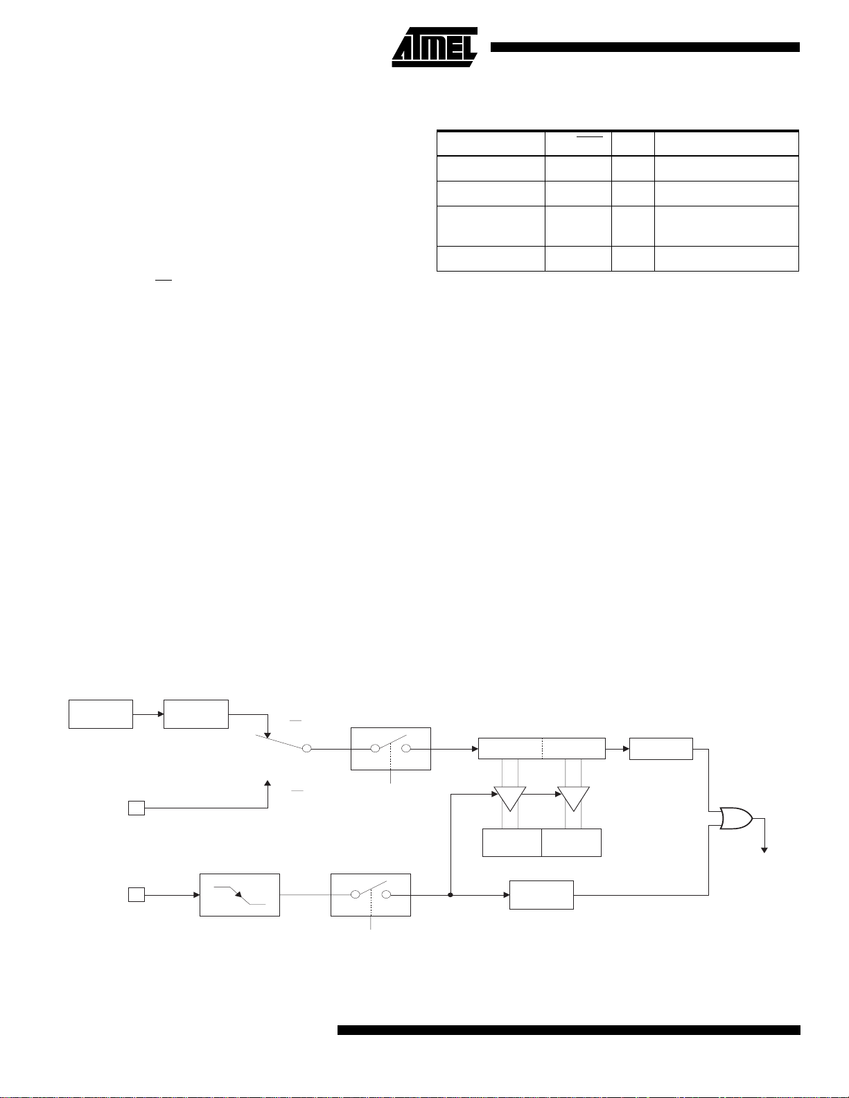
SPI Block Diagram
OSCILLATOR
DIVIDER
÷4÷16÷64÷128
SELECT
SPR1
SPI CONTROL
WCOL
SPIF
SPI STATUS REGISTER
SPR0
MSB
8/16-BIT SHIFT REGISTER
SPI CLOCK (MASTER)
MSTR
SPE
8
READ DATA BUFFER
CLOCK
8
SPIE
SPE
DORD
MSTR
SPI CONTROL REGISTER
8
LSB
CLOCK
LOGIC
CPOL
CPHA
SPR1
SPR0
S
M
M
S
S
M
MSTR
PIN CONTROL LOGIC
SPE
DORD
MISO
P1.6
MOSI
P1.5
SCK
1.7
SS
P1.4
4-262
SPI INTERRUPT
REQUEST
AT89LS53
INTERNAL
DATA BUS
Page 15

AT89LS53
The interconnection between master and slave CPUs with
SPI is shown in the following figure. The SCK pin is the
clock output in the master mode but is the clock input in the
slave mode. Writing to the SPI data register of the master
CPU starts the SPI clock generator, and the data written
shifts out of the MOSI pin and in to the MOSI pin of the
slave CPU. After sh ifting one by te, the SPI clo ck g enerator
stops, setting the end of transmission flag (SPIF). If both
the SPI interrupt enab le bit (S PIE) and the ser ial por t inter rupt enable bit (ES) are set, an interrupt is requested.
Figure 7.
SPI Master-Slave Interconnection
MSB LSB
MASTER
8-BIT SHIFT REGISTER
The Slave Select input, SS
individual SPI device as a slave. When SS
the SPI port is deactivated and the MOSI/P1.5 pin can be
used as an input.
There are four combinations of SCK phase and polarity
with respect to serial data, which are determined by control
bits CPHA and CPOL. The SPI data transfer formats are
shown in Figures 8 and 9.
MISO
MISO
MSB LSB
/P1.4, is set low to select an
/P1.4 is set high,
SLAVE
8-BIT SHIFT REGISTER
MOSI MOSI
SPI
CLOCK GENERATOR
Figure 8.
*Not defined but normally MSB of character just received
SPI transfer Format with CPHA = 0
SCK
SS SS
V
SCK
CC
4-263
Page 16

Figure 9.
SPI Transfer Format with CPHA = 1
SCK CYCLE #
(FOR REFERENCE)
1 2 3 4 5 6 7 8
SCK (CPOL=0)
SCK (CPOL=1)
MOSI
MSB 6 5 4 3 2
(FROM MASTER)
MISO
(FROM SLAVE)
MSB
*
65432
SS (TO SLAVE)
*Not defined but normally LSB of previously transmitted character
Interrupts
The AT89LS53 has a total of six interrupt vectors: two
external interrupts (INT0
(Timers 0, 1, and 2), and the serial port interrupt. Thes e
interrupts are all shown in Figure 10.
Each of these interrupt sources can be individually enabled
or disabled by setting or clearing a bit in Special F unction
Register IE. IE also contains a global disable bit, EA, which
disables all interrupts at once.
Note that Table 10 shows that bit position IE.6 is unimplemented. In the AT89C51 and AT89LV51, bit position IE.5 is
also unimplemented. User software should not write 1s to
and INT1), three timer interrupts
these bit positions, since they may be used in future AT89
products.
Timer 2 interrupt is gene ra ted b y th e logi cal OR of bits TF2
and EXF2 in register T2CON. Neither of these flags is
cleared by hardware when the se rvice rout ine is vect ored
to. In fact, the service routine may have to d etermine
whether it was TF2 or EXF2 that generated the interrupt,
and that bit will have to be cleared in software.
The Timer 0 and Timer 1 flags, TF0 and TF1, are set at
S5P2 of the cycle in which the timers overflow. The values
are then polled by the circuitry in the next cycle. However,
the Timer 2 flag, TF2, is set at S2P2 and is polled in the
same cycle in which the timer overflows.
1 LSB
1 LSB
Table 10.
(MSB) (LSB)
Symbol Position Function
User software should never write 1s to unimplemented bits, because
they may be used in future AT89 products.
Interrupt Enable (IE) Register
EA — ET2 ES ET1 EX1 ET0 EX0
Enable Bit = 1 enables the interrupt.
Enable Bit = 0 disables the interrupt.
Disables all interrupts. If EA = 0, no interrupt
EA IE.7
— IE.6 Reserved.
ET2 IE.5 Timer 2 interrupt enable bit.
ES IE.4 SPI and UART interrupt enable bit.
ET1 IE.3 Timer 1 interrupt enable bit.
EX1 IE.2 Exter nal interr upt 1 enable bit.
ET0 IE.1 Timer 0 interrupt enable bit.
EX0 IE.0 Exter nal interr upt 0 enable bit.
is acknowledged. If EA = 1, each interrupt
source is individually enabled or disabled by
setting or clearing its enable bit.
Figure 10.
Interrupt Sources
4-264
AT89LS53
Page 17

AT89LS53
Figure 11.
Note: C1, C2 = 30 pF ± 10 pF for Crystals
Oscillator Connections
= 40 pF ± 10 pF for Ceramic Resonators
Oscillator Characteristics
XTAL1 and XTAL2 ar e the inp ut and output, respecti vely,
of an inverting ampli fier that ca n be confi gured for u se as
an on-chip oscillator, as shown in Figure 11. Either a quartz
crystal or ceramic resonator may be used. To drive the
device from an external clock source, XTAL2 should be left
unconnected while XTAL1 is driven, as shown in Figure 12.
There are no requirements on the duty cycle of the external
clock signal, since the input to the internal clocking circuitry
is through a divide-by- two flip-flo p, but mini mum and max imum voltage high and low time specificati ons must be
observed.
Idle Mode
In idle mode, the CPU puts itself to sleep while all the onchip peripherals remain active. The mode is invoked by
software. The content of the on-chip RAM and all the special functions re gisters remain unc hanged during this
mode. The idle mode can be terminated by any e nabled
interrupt or by a hardware reset.
Note that when idle mod e is terminated by a ha rdware
reset, the devi ce normally r esumes prog ram executio n
from where it left off, up to two machine cycles before the
Figure 12.
internal reset algori thm takes control. On-chip hardware
inhibits access to i nternal RAM i n this event, bu t access to
the port pins is not inhibited. To eliminate the possibility of
an unexpected write to a port pin when idle mode is terminated by a reset, the instruction following the one that
invokes idle m ode s houl d not wri te to a po rt pin or to ex ter nal memory.
External Clock Drive Configuration
Power Down Mode
In the power down mode, the oscillator is stopped and the
instruction that invoke s power down is the last instr uction
executed. The on-chip RAM and Special Function Registers retain their values until th e power dow n mode i s terminated. Exit from power down can be initiated either by a
hardware reset or by an enabled external inte rrupt. Reset
redefines the SFRs but doe s not cha nge the o n-ch ip RAM.
The reset should not be activated be fore V
its normal operating level and must be held active long
enough to allow the oscillator to restart and stabilize.
To exit power down via an interrupt, the external interrupt
must be enabled as level sensiti ve before entering power
down. The interrupt service routine starts at 16 ms (no minal) after the enabled interrupt pin is activated.
is restored to
CC
Status of External Pins During Idle and Power Down Modes
Mode Program Memory ALE PSEN PORT0 PORT1 PORT2 PORT3
Idle Internal 1 1 Data Data Data Data
Idle External 1 1 Float Data Address Data
Power Down Internal 0 0 Data Data Data Data
Power Down External 0 0 Float Data Data Data
4-265
Page 18

Program Memory Lock Bits
The AT89LS53 has three lock bits that can be left unprogrammed (U) or can be programmed (P) to obtain the additional features listed in the following table.
When lock bit 1 is programmed, the logic level at the EA
is sampled and latched during rese t. If the device is powered up without a reset, the latch initi alizes to a random
Lock Bit Protection Modes
Program Lock Bits
Protection TypeLB1 LB2 LB3
1 U U U No internal memory lock feature.
MOVC instructions executed from external program memory are disabled from fetching
2PUU
3 P P U Same as Mode 2, but parallel or serial verify are also disabled.
4 P P P Same as Mode 3, but external execution is also disabled.
Notes: 1. U = Unprogrammed
2. P = Programmed
code bytes from internal memory. EA
programming of the Flash memory (parallel or serial mode) is disabled.
(1) (2)
pin
value and holds that value until reset is activated. The
latched value of EA
at that pin in order for the device to function properly.
Once programmed, the lock bits can only be unprogrammed with the Chip Erase operations in either the parallel or serial modes.
is sampled and latched on reset and further
must agree wi th the cu rre nt logic level
Programming the Flash
Atmel’s AT89LS5 3 Flash M icrocontro ller offers 12K by tes
of in-system reprogrammable Flash Code memory.
The AT89LS53 is normally shipped with the on-chip Flash
Code memory array in the erased state (i.e. contents =
FFH) and ready to be progr am me d. Thi s dev i ce su ppo rts a
High-Voltage (12V) Parallel programming mode and a LowVoltage (2.7 to 6.0V) Serial progr amming mode. The se rial
programming mode provides a c onvenient way to download the AT89LS53 ins ide the user ’s system . The parallel
programming mode is compatible with conventional third
party Flash or EPROM programmers.
The Code memory ar ray occ upies one c ontig uous a ddres s
space from 0000H to 2FFFH.
The Code array on th e AT8 9LS5 3 is prog ramm ed b yte-by byte in either programming mode. An auto-erase cycle is
provided with the self-timed programming operation in the
serial programming mode. Th ere is no need to perfor m the
Chip Erase operation to reprog ram an y memo ry lo catio n in
the serial programming mode unless any of the lock bits
have been programmed.
In the parallel prog ramming mode, th ere is n o auto-e rase
cycle. To reprogram any non- blank by te, the user ne eds to
use the Chip Erase operation first to eras e the entire Code
memory array.
Parallel Programming Algorithm
To program and verify the AT89LS53 in the parallel programming mode, the following sequence is recommended:
1. Power-up sequence:
Apply power between V
Set RST pin to “H”.
Apply a 3 MHz to 12 MHz clock to XTAL 1 pin and wait
for at least 10 milliseconds.
2. Set PSEN
ALE pin to “H”
pin to “H” and all other pins to “H”.
EA
3. Apply the appropriate combination of “H” or “L” logic
levels to pins P2.6, P2.7, P3.6, P3.7 to select one of
the programming operations shown in the Flash
Programming Modes table.
4. Apply the desired byte address to pins P1.0 to P1.7
and P2.0 to P2.5.
Apply data to pins P 0.0 to P0.7 for Write Code operation.
5. Raise EA
erase or verification.
6. Pulse ALE/PROG
Code memory array, or the lock bits. The byte-write
cycle is self-timed and typically takes 1.5 ms.
pin to “L”
/VPP to 12V to enable Flash p rogrammin g,
once to program a byte in the
and GND pins.
CC
4-266
AT89LS53
Page 19

AT89LS53
7. To verify the byte just programmed, bring pin P2.7 to
“L” and read the programmed data at pins P0.0 to
P0.7.
8. Repeat steps 3 through 7 changing the address and
data for the entire 12K-byte array or until the end of
the object file is reached.
9. Power-off sequence:
Set XTAL1 to “L”.
Set RST and EA
Tur n V
power off.
CC
pins to “L”.
DATA Polling
The AT89LS53 features DATA Polling to indicate the end of
a write cycle. During a write cycle in the parallel or serial
programming mode, an attempted read of the last byte written will result in the complement of the written datum on
P0.7 (parallel mode), and on the MSB of the se rial output
byte on MISO (serial mode). Once the write cycle has been
completed, true data are valid on all outputs, and the next
cycle may begin. DATA
write cycle has been initiated.
Polling may begin any time after a
Ready/Busy
The progress of b yte pro gramm ing in the par all el prog ramming mode can also b e monitore d by the RDY /BSY
signal. Pin P3.4 is pulled Low after ALE goes High during
programming to indicate BUSY
when programming is done to indicate READY.
. P3.4 is pulled High again
output
Program Verify
If lock bits LB1 and LB2 have not been programmed, the
programmed Code can be read back via the addres s and
data lines for verification. The state of the lock bits can also
be verified directly in the parallel programming mode. In the
serial programming mode, the state of the lock bits can only
be verified indirectly by observing that the lock bit features
are enabled.
Chip Erase
In the parallel programming mode, chip erase is initiated by
using the proper comb ination of control s ignals and by
holding ALE/PROG
ten with all “1”s in the Chip Erase operation.
In the serial programming mode, a chip erase operation is
initiated by issuing the Chip Erase instruction. In this mode,
chip erase is self-timed and takes about 16 ms.
During chip erase, a serial read from any address location
will return 00H at the data outputs.
low for 10 ms. The Code array is writ-
Serial Programming Fuse
A programmable fuse is available to disable Serial Programming if the user needs maximum system security. The
Serial Programming Fuse can only be programmed or
erased in the Parallel Programming Mode.
The AT89LS53 is shipped with the Serial Programming
Mode enabled.
Reading the Signature Bytes:
read by the same procedure as a normal verification of
locations 030H and 031H , excep t that P3 .6 and P3 .7 must
be pulled to a logic low. The values returned are as follows:
(030H) = 1EH indicates manufactured by Atmel
(031H) = 63H indic at e s 89L S53
The signature bytes are
Programming Interface
Every code byte in the Flash array can be written, and the
entire array can be erased, by using the appropriate combination of control signals. The write operation cycle is s elftimed and once initiated, will automatically time itself to
completion.
All major programmi ng ve ndors of fer worl dwide s upport fo r
the Atmel microcontroller series. Please contact your local
programming vendor for the appropriate software revision.
Serial Downloading
The Code memory array can be programmed using the
serial SPI bus while RST is pulled to V
face consists of pins SCK, MOSI (input) and MISO (output).
After RST is set high, the Programming Enable instruction
needs to be executed first before program/erase operations
can be executed.
An auto-erase cycle is built into the self-timed programming
operation (in the serial mode ONLY) and there is no need
to first execute the Chip Erase instruction unless any of the
lock bits have been programmed. The Chip Erase operation turns the content of every memory location in the Code
array into FFH.
The Code memory array has an address space of 0000H to
2FFFH.
Either an external system clock is supplied at pin XTAL1 or
a crystal needs to be connected across pins XTAL1 and
XTAL2. The maximum serial c lo ck ( SCK) freque nc y s hou ld
be less than 1/40 of the crystal frequency. With a 12 MHz
oscillator clock, the maximum SCK frequency is 300 KHz.
. The serial inter-
CC
4-267
Page 20

Serial Programming Algorithm
To program and verify the AT89LS53 in the serial programming mode, the following sequence is recommended:
1. Power-up sequence:
Apply power between V
and GND pins.
CC
Set RST pin to “H”.
If a crystal is not connected across pins XTAL1 and
XTAL2, apply a 3 M Hz to 12 MHz clock to XTAL1 pi n
and wait for at least 10 milliseconds.
2. Enable serial programming by sending the Programming Enable serial instruction to pin MOSI/
P1.5. The frequency of the shift clock supplied at
pin SCK/P1.7 needs to be less than the CPU clock
at XTAL1 divided by 40.
3. The Code array is programmed one byte at a time
by supplying the address and data together with the
appropriate Write instruction. The selected memory
location is first automatically erased before new
data is written. The write cycle is self-timed and typically takes less than 2.5 ms at 5V and less than 10
ms at 2.7V.
Instruction Set
4. Any memory location can be verified by using the
Read instruction which returns the content at the
selected address at serial output MISO/P1.6.
5. At the end of a programming session, RST can be
set low to commence normal operation.
Power-off sequence (if needed):
Set XTAL1 to “L” (if a crystal is not used).
Set RST to “L”.
Tur n V
power off.
CC
Serial Programming Instruction
The Instruction Set for Serial Programming follows a 3-byte
protocol and is shown in the following table:
Input Format
Instruction
Byte 1 Byte 2 Byte 3
Operation
Programming Enable 1010 1100 0101 0011 xxxx xxxx Enable serial programming interface after RST goes
high.
Chip Erase 1010 1100 xxxx x100 xxxx xxxx Chip erase the 12K memory array.
Read Code Memory low addr xxxx xxxx Read data from Code memory array at the selected
A12
A11
A10
A9
A8
01
A13
address. The 6 MSBs of the first byte are the high order
address bits. The low order address bits are in the
second byte. Data are available at pin MISO during the
third byte.
Write Code Memory low addr data in Write data to Code memory location at selected
A12
A11
10
A9
A8
A10
A13
address. The address bits are the 6 MSBs of the first
byte together with the second byte.
Write Lock Bits 1010 1100 xxxx xxxx Write lock bits.
Notes: 1. DATA polling is used to indicate the end of a write cycle which typically takes less than 10 ms at 2.7V.
2. “x” = don’t care.
LB1
LB2
xx111
LB3
Set LB1, LB2 or LB3 = “0” to program lock bits.
4-268
AT89LS53
Page 21

Flash Parallel Prog ram ming Modes
AT89LS53
Mode RST PSEN ALE/ PROG EA/V
Serial Prog. Modes H h
Chip Erase H L 12V H L L L X X
Write (12K bytes) Memory H L 12V L H H H DIN ADDR
Read (12K bytes) Memory H L H 12V L L H H DOUT ADDR
Write Lock Bits: H L 12V H L H L DIN X
Bit - 1 P0.7 = 0 X
Bit - 2 P0.6 = 0 X
Bit - 3 P0.5 = 0 X
Read Lock Bits: H L H 12V H H L L DOUT X
Bit - 1 @P0.2 X
Bit - 2 @P0.1 X
Bit - 3 @P0.0 X
Read Atmel Code H L H 12V L L L L DOUT 30H
Read Device Code H L H 12V L L L L DOUT 31H
Serial Prog. Enable H L 12V L H L H P0.0 = 0 X
Serial Prog. Disable H L 12V L H L H P0.0 = 1 X
Read Serial Prog. Fuse H L H 12V H H L H @P0.0 X
(1)
(1)
h
(2)
(2)
(2)
P2.6 P2.7 P3.6 P3.7
PP
x
Data I/O
P0.7:0
Address
P2.5:0 P1.7:0
Notes: 1. “h” = weakly pulled “High” internally.
2. Chip Erase and Serial Programming Fuse require a 10-ms PROG pulse. Chip Erase needs to be performed first before
reprogramming any byte with a content other than FFH.
3. P3.4 is pulled Low during programming to indicate RDY/BSY.
4. “X” = don’t care
4-269
Page 22

Figure 13.
Programming the Flash Memory
Figure 14.
Flash Serial Downloading
+
Figure 15.
Verifying the Flash Memory
4-270
AT89LS53
Page 23

AT89LS53
Flash Programming and Verification Characteristics - Parallel Mode
TA = 0°C to 70°C, VCC = 5.0V ± 10%
Symbol Parameter Min Max Units
V
PP
I
PP
1/t
CLCL
t
AVGL
t
GHAX
t
DVGL
t
GHDX
t
EHSH
t
SHGL
t
GLGH
t
AVQV
t
ELQV
t
EHQZ
t
GHBL
t
WC
Programming Enable Voltage 11.5 12.5 V
Programming Enable Current 1.0 mA
Oscillator Frequency 3 12 MHz
Address Setup to PROG Low 48t
Address Hold After PROG 48t
Data Setup to PROG Low 48t
Data Hold After PROG 48t
P2.7 (ENABLE) High to V
PP
48t
CLCL
CLCL
CLCL
CLCL
CLCL
VPP Setup to PROG Low 10 µs
PROG Width 1 110 µs
Address to Data Valid 48t
ENABLE Low to Data Valid 48t
Data Float After ENABLE 0 48t
CLCL
CLCL
CLCL
PROG High to BUSY Low 1.0 µs
Byte Write Cycle Time 2.0 ms
4-271
Page 24

Flash Programming and Verification Waveforms - Parallel Mode
Serial Downloading Waveforms
SERIAL CLOCK INPUT
SCK/P1.7
SERIAL DATA INPUT
MOSI/P1.5
SERIAL DATA OUTPUT
MISO/P1.6
7
MSB
MSB
4
6
5
3
2
1
0
LSB
LSB
4-272
AT89LS53
Page 25

Absolute Maximum Ratings*
AT89LS53
Operating Temperature......................-55°C to +125°C
*NOTICE: Stresses beyond those listed under “Absolute
Maximum Ratings” may cause permanent dam-
Storage Temperature.........................-65°C to +150°C
age to the dev ice . This is a stress ra ting onl y and
functional oper ati on of the device at thes e or any
Voltage on Any Pin
with Respect to Ground........................-1.0V to +7.0V
Maximum Operating Voltage................................6.6V
other conditions beyond those indicated in the
operational sections of this specification is not
implied. Exposure to absolute maximum rating
conditions f or exten ded periods may af fect de vice
reliability.
DC Output Current .........................................15.0 mA
DC Characteristics
The values shown in this table are valid for TA = -40°C to 85°C and VCC = 2.7V to 6.0V, unless otherwise noted.
Symbol Parameter Condition Min Max Units
V
V
V
V
V
V
IL
IL1
IH
IH1
OL
OL1
Input Low Voltage (Except EA)-0.50.2 V
Input Low Voltage (EA)-0.50.2 V
- 0.1 V
CC
- 0.3 V
CC
Input High Voltage (Except XTAL1, RST) 0.2 VCC + 0.9 VCC + 0.5 V
Input High Voltage (XTAL1, RST) 0.7 V
Output Low Voltage
(Ports 1,2,3)
Output Low Voltage
(Port 0, ALE, PSEN)
(1)
(1)
= 1.6 mA 0.5 V
I
OL
= 3.2 mA 0.5 V
I
OL
CC
VCC + 0.5 V
= -60 µA, VCC = 5V ± 10% 2.4 V
I
V
OH
Output High Voltage
(Ports 1,2,3, ALE, PSEN
)
OH
I
= -25 µA0.75 VCCV
OH
IOH = -10 µA 0.9 V
CC
IOH = -800 µA, VCC = 5V ± 10% 2.4 V
V
I
I
I
OH1
IL
TL
LI
Output High Voltage
(Port 0 in External Bus Mode)
Logical 0 Input Current (Ports 1,2,3) VIN = 0.45V -50
Logical 1 to 0 Transition Current (Ports 1,2,3) VIN = 2V -650
Input Leakage Current
(Port 0, EA)
I
= -300 µA0.75 VCCV
OH
IOH = -80 µA 0.9 V
0.45 < V
IN
< V
CC
CC
10
±
RRST Reset Pulldown Resistor 50 300 K
C
IO
Pin Capacitance Test Freq. = 1 MHz, TA = 25°C 10 pF
Active Mode, 12 MHz 25 mA
Power Supply Current
Idle Mode, 12 MHz 6.5 mA
I
CC
Power Down Mode
(2)
VCC = 6V 100
VCC = 3V 40
Notes: 1. Under steady state (non-transient) conditions, IOL
must be externally limited as follows :
Maximum I
Maximum I
per port pin: 10 mA
OL
per 8-bit port:
OL
Port 0: 26 mA
Maximum total I
exceeds the test condition, V
If I
OL
related specification. Pins are not guaranteed to sink
current greater than the listed test conditions.
2. Min imum VCC for Power Down is 2V
for all output pins: 71 mA
OL
may exceed the
OL
Ports 1,2, 3: 15 mA
V
V
A
µ
A
µ
A
µ
Ω
A
µ
A
µ
4-273
Page 26

AC Characteristics
Under operating conditions, load capacitance for Port 0, ALE/PROG, and PSEN = 100 pF; load capacitance for all other
outputs = 80 pF.
External Program and Data Memory Characteristics
12MHz Oscillator Variable Oscillator
Symbol Parameter
1/t
CLCL
t
LHLL
t
AVLL
t
LLAX
t
LLIV
t
LLPL
t
PLPH
t
PLIV
t
PXIX
t
PXIZ
t
PXAV
t
AVIV
t
PLAZ
t
RLRH
t
WLWH
t
RLDV
t
RHDX
t
RHDZ
t
LLDV
t
AVDV
t
LLWL
t
AVWL
t
QVWX
t
QVWH
t
WHQX
t
RLAZ
t
WHLH
Oscillator Frequency 0 12 MHz
ALE Pulse Width 127 2t
Address Valid to ALE Low 43 t
Address Hold After ALE Low 48 t
ALE Low to Valid Instruction In 233 4t
ALE Low to PSEN Low 43 t
PSEN Pulse Width 205 3t
PSEN Low to Valid Instruction In 145 3t
Input Instruction Hold After PSEN 00 ns
Input Instruction Float After PSEN 59 t
PSEN to Address Valid 75 t
Address to Valid Instruction In 312 5t
PSEN Low to Address Float 10 10 ns
RD Pulse Width 400 6t
WR Pulse Width 400 6t
RD Low to Valid Data In 252 5t
Data Hold After RD 00 ns
Data Float After RD 97 2t
ALE Low to Valid Data In 517 8t
Address to Valid Data In 585 9t
ALE Low to RD or WR Low 200 300 3t
Address to RD or WR Low 203 4t
Data Valid to WR Transition 23 t
Data Valid to WR High 433 7t
Data Hold After WR 33 t
RD Low to Address Float 0 0 ns
RD or WR High to ALE High 43 123 t
- 40 ns
CLCL
- 40 ns
CLCL
- 35 ns
CLCL
- 100 ns
CLCL
- 40 ns
CLCL
- 45 ns
CLCL
- 105 ns
CLCL
- 25 ns
CLCL
- 8 ns
CLCL
- 105 ns
CLCL
- 100 ns
CLCL
- 100 ns
CLCL
- 165 ns
CLCL
- 70 ns
CLCL
- 150 ns
CLCL
- 165 ns
CLCL
- 50 3t
CLCL
- 130 ns
CLCL
- 60 ns
CLCL
- 150 ns
CLCL
- 50 ns
CLCL
- 40 t
CLCL
+ 50 ns
CLCL
+ 40 ns
CLCL
UnitsMin Max Min Max
4-274
AT89LS53
Page 27

External Program Memory Read Cycle
AT89LS53
External Data Memory Read Cycle
4-275
Page 28

External Data Memory Write Cycle
External Clock Drive Waveforms
Exter nal Clock Drive
Symbol Parameter
1/t
CLCL
t
CLCL
t
CHCX
t
CLCX
t
CLCH
t
CHCL
4-276
Oscillator Frequency 0 12 MHz
Clock Period 83.3 ns
High Time 30 ns
Low Time 30 ns
Rise Time 20 ns
Fall Time 20 ns
AT89LS53
= 2.7V to 6.0V
V
CC
Min Max Units
Page 29

Serial Port Timing: Shift Register Mode Test Conditions
The values in this table are valid for VCC = 2.7V to 6V and Load Capacitance = 80 pF.
12 MHz Oscillator Variable Oscillator
AT89LS53
Symbol Parameter
t
XLXL
t
QVXH
t
XHQX
t
XHDX
t
XHDV
Serial Port Clock Cycle Time 1.0 12t
Output Data Setup to Clock
Rising Edge
Output Data Hold After Clock
Rising Edge
Input Data Hold After Clock
Rising Edge
Clock Rising Edge to Input Data
Valid
Min Max Min Max
700 10t
50 2t
00ns
Shift Register Mode Timing Waveforms
CLCL
- 133 ns
CLCL
- 117 ns
CLCL
700 10t
- 133 ns
CLCL
Units
µs
AC Testing Input/Output Waveforms
Notes: 1. AC Inputs during testing are driven at VCC - 0.5V
for a logic 1 and 0.45V for a logic 0. Timing measurements are made at VIH min. for a logic 1 and VIL
max. for a logic 0.
(1)
Float Waveforms
Notes: 1. For timing purposes, a port pin is no longer floating
when a 100 mV change fro m load voltage occurs. A
port pin begins to float when a 100 mV change from
the loaded V
(1)
OH/VOL
level occurs.
4-277
Page 30

C
C
m
A
AT89LS53
24
20
V = 6.0V
CC
I
16
V = 5.0V
TYPICAL ICC (ACTIVE) at 25°C
12
8
CC
V = 3.0V
CC
TYPICAL ICC vs. VOLTAGE - POWERDOWN (85°C)
20
15
I
C
C
10
µ
A
5
AT89LS53
4
0
0
4 8 12 16 20 24
F (MHz)
0
3.0V
Notes: 1. XTAL1 tied to GND for ICC (power down)
2. Lock bits programmed
4.0V 5.0V 6.0V
V VOLTAGE
CC
AT89LS53
TYPICAL ICC (IDLE) at 25°C
V=
6.0V
CC
V=
5.0V
CC
V=
3.0V
CC
m
4.8
4.0
I
3.2
C
C
2.4
1.6
A
0.8
0.0
0
4 8 12 16 20 24
F (MHz)
4-278
AT89LS53
Page 31

Ordering Information
AT89LS53
Speed
(MHz)
12 2.7V to 6.0V AT89LS53-12AC
Power
Supply
2.7V to 6.0V AT89LS53-12AI
Ordering Code Package Operation Range
AT89LS53-12JC
AT89LS53-12PC
AT89LS53-12JI
AT89LS53-12PI
44A
44J
40P6
44A
44J
40P6
Commercial
(0°C to 70°C)
Industrial
(-40°C to 85°C)
44A
44J
40P6
Package Type
44 Lead, Thin Plastic Gull Wing Quad Flatpack (TQFP)
44 Lead, Plastic J-Leaded Chip Carrier (PLCC)
40 Lead, 0.600" Wide, Plastic Dual Inline Package (PDIP)
4-279
 Loading...