

Page 1

Features
• Protocol
– USB Used as a Physical Layer
– Device Firmware Upgrade Class Compliant
– Auto-Frequency Detection
• In-System Programming
– Read/Write Flash Memory
– Read Device ID
– Full-chip Erase
– Read/Write Configuration Bytes
– Security Setting from ISP Command
– Remote Application Start Command
• In-Application Programming/Self-Programming
– Read/Write Flash Memory
– Read Device ID
– Block Erase
– Read/Write Configuration Bytes
– Bootloader Start
Description
This document describes the USB bootloader functionality as well as the USB protocol to efficiently perform operations on the on-chip Flash memory. Additional
information on the AT89C5132 product can be found in the AT89C5132 datasheet and
the AT89C5132 errata sheet available on the Atmel web site, www.atmel.com.
The bootloader software (binary file) currently used for production is available from the
Atmel web site.
USB
Microcontrollers
AT89C5132
USB Bootloader
Bootloader Revision Purpose of Modifications Date
Revisions 1.6.2 and higher First release 3/25/2003
Rev. 4256A–USB–06/03
1
Page 2
Functional Description
The AT89C5132 USB Bootloader facilitates In-System Programming (ISP) and In-Application Programming (IAP) .
In-System Programming Capability
In-Application
Programming or SelfProgramming Capability
In-System Programming allows the user to program or reprogram the microcontroller
on-chip Flash memory without removing it from the system and without the need of a
pre-programmed application.
The USB bootloader can manage a communication with a host through the USB bus. It
can also access and perform requested operations on the on-chip Flash memory.
IAP allows the reprogramming of the microcontroller on-chip Flash memory without
removing it from the system and while the embedded application is running.
The USB bootloader contains some Application Programming Interface routines named
API routines allowing IAP by using the user’s firmware.
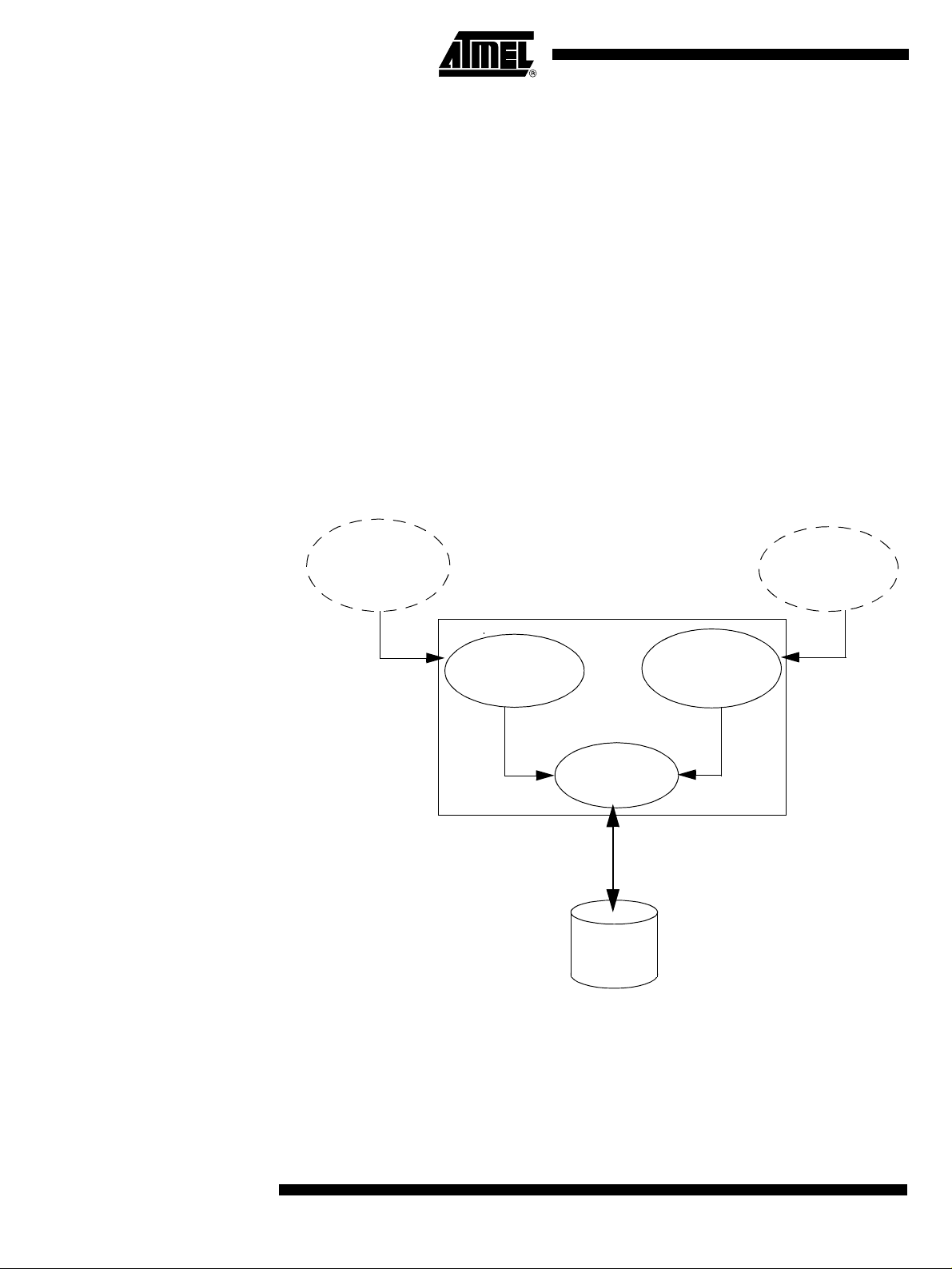
Block Diagram This section describes the different parts of the USB bootloader. Figure 1 shows the on-
chip bootloader and IAP processes.
Figure 1. Bootloader Process Description
External host via the
USB Protocol
Communication
ISP Communication
Management
IAP
User Call
Management
On-chip
User
Application
Flash Memory
Management
Flash
Memory
2
AT89C5132
4256A–USB–06/03
Page 3

AT89C5132
ISP Communication Management
The purpose of this process is to manage the communication and its protocol between
the on-chip bootloader and an external device (host). The on-chip bootloader implements a USB protocol (see Section “Protocol”, page 10). This process translates serial
communication frames (USB) into Flash memory accesses (read, write, erase...).
User Call Management Several Application Program Interface (API) calls are available to the application pro-
gram to selectively erase and program Flash pages. All calls are made through a
common interface (API calls) included in the bootloader. The purpose of this process is
to translate the application request into internal Flash memory operations.
Flash Memory Management This process manages low level accesses to the Flash memory (performs read and
write accesses).
Bootloader Configuration
Configuration and Manufacturer Information
The following table lists Configuration and Manufacturer byte information used by the
bootloader. This information can be accessed through a set of API or ISP commands.
Tab le 1 . Configuration and Manufacturer Byte Information
Mnemonic Description Default Value
BSB Boot Status Byte FFh
SBV Software Boot Vector FOh
SSB Software Security Byte FFh
Mapping and Default Value of Hardware Security Byte
EB Extra Byte FFh
Manufacturer 58h
Id1: Family Code D7h
Id2: Product Name F7h
Id3: Product Revision DFh
The 4 MSB of the Hardware Byte can be read/written by software (this area is called
Fuse bits). The 4 LSB can only be read by software and written by hardware using parallel programmer devices, this area is called Lock bits.
Tab le 2. Hardware Byte Information
Bit Position Mnemonic Default Value Description
7 X2B U To start in x1 mode
6 BLJB P To map the boot area in code area between F000h-FFFFh
5– U
4– U
3 reserved U
2LB2 P
To lock the chip (see datasheet)1LB1 U
4256A–USB–06/03
0LB0 U
Note: U: Unprogrammed = 1
P: Program = 0
3
Page 4

Security The bootloader has Software Security Byte (SSB) to protect itself from user access or
ISP access.
The Software Security Byte (SSB) protects from ISP accesses. The command ’Program
Software Security Bit’ can only write a higher priority level. There are three levels of
security:
• Level 0: NO_SECURITY (FFh)
This is the default level.
From level 0, one can write level 1 or level 2.
• Level 1: WRITE_SECURITY (FEh)
In this level it is impossible to write in the Flash memory.
The Bootloader returns an err_WRITE status.
From level 1, one can write only level 2.
• Level 2: RD_WR_SECURITY (FCh)
Level 2 forbids all read and write accesses to/from the Flash memory.
The Bootloader returns an err_WRITE or an err_VENDOR status.
Only a full chip erase command can reset the software security bits.
Tab le 3 . Security Levels
Level 0 Level 1 Level 2
Flash Any access allowed Read only access allowed All access not allowed
Fuse bit Any access allowed Read only access allowed All access not allowed
BSB & SBV & EB Any access allowed Any access allowed Any access allowed
SSB Any access allowed Write level2 allowed Read only access allowed
Manufacturer info Read only access allowed Read only access allowed Read only access allowed
Bootloader info Read only access allowed Read only access allowed Read only access allowed
Erase block Allowed Not allowed Not allowed
Full chip erase Allowed Allowed Allowed
Blank Check Allowed Allowed Allowed
4
AT89C5132
4256A–USB–06/03
Page 5

AT89C5132
Software Boot Vector The Software Boot Vector (SBV) forces the execution of a user bootloader starting at
address [SBV]00h in the application area (FM0).
The way to start this user bootloader is described in Section “Bootloader Configuration”.
USB Bootloader
User Bootloader
Application
FM0
[SBV]00h
FLIP Software Program FLIP is a PC software program running under Windows
that supports all Atmel Flash microcontrollers and USB protocol communication media.
This free software program is available from the Atmel web site.
FM1
®
9x/Me/2000/XP and LINUX
®
4256A–USB–06/03
5
Page 6

In-System Programming
The ISP allows the user to program or reprogram the microcontroller’s on-chip Flash
memory through the serial line without removing it from the system and without the need
of a pre-programmed application.
This section describes how to start the UART bootloader and the higher level protocol
over the serial line.
Bootloader Execution As internal C51 code space is limited to 64K bytes, some mechanisms are implemented
to allow boot memory to be mapped in the code space for execution at addresses F000h
to FFFFh. The boot memory is enabled by setting the ENBOOT bit in AUXR1. The three
ways to set this bit are detailed below.
Software Boot Mapping The software way to set ENBOOT consists in writing to AUXR1 from the user’s soft-
ware. This enables bootloader or API routines execution.
Hardware Condition Boot Mapping
Programmed Condition Boot Mapping
The hardware condition is based on the ISP# pin. When driving this pin to low level, the
chip reset sets ENBOOT and forces the reset vector to F000h instead of 0000h in order
to execute the bootloader software.
As shown in Figure 2, the hardware condition always allows In-System recovery when
user’s memory has been corrupted.
The programmed condition is based on the Bootloader Jump Bit (BLJB) in HSB. As
shown in Figure 2, this bit is programmed (by hardware or software programming
mode), the chip reset set ENBOOT and forces the reset vector to F000h instead of
0000h, in order to execute the bootloader software.
6
AT89C5132
4256A–USB–06/03
Page 7
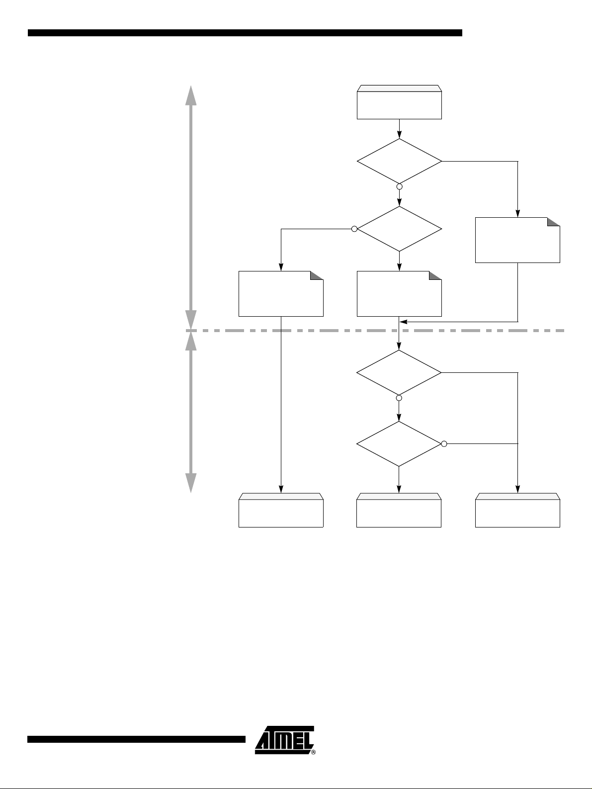
Figure 2. Boot Process Algorithm
AT89C5132
RESET
Hard Cond?
ISP# = L?
HardwareSoftware
Standard Init
ENBOOT = 0
PC = 0000h
FCON = F0h
Process Process
User’s
Application
Prog Cond?
BLJB = P?
Prog Cond Init
ENBOOT = 1
PC = F000h
FCON = F0h
Hard Init?
FCON = 00h?
User Boot?
SBV < F0h?
User’s
Bootloader
Hard Cond Init
ENBOOT = 1
PC = F000h
FCON = 00h
Atmel’s
Bootloader
4256A–USB–06/03
7
Page 8
Physical Layer The USB norm specifies all the transfers over the USB line. The USB specification also
includes several CLASS and SUB-CLASS specifications. These stand-alone documents
are used by the manufacturer to implement a USB link between a PC and a device supporting the In-System Programming. Mostly, the USB specification is implemented by
hardware (automatic reply, handshakes, timings, ...) and the USB Classes and SubClasses are implemented by software at a data level.
Figure 3. USB Bus Topography
Downstream Transfer: OUT
Upstream Transfer: IN
48 MHz Frequency Autogeneration
PC driver
PC application
USB line
application (Device)
PC (Host)
The USB used to transmit information has the following configuration:
• USB DFU using the Default Control Endpoint only (endpoint 0) with a 32 bytes
length.
• 48 MHz for USB controller: frequency auto-detection performed by the bootloader.
The following table shows the allowed frequencies compatible with the USB bootloader
48 MHz auto-generation.
12 MHz 16 MHz 20 MHz
X1 - X2 OK OK OK
Device Driver/API
Firmware
8
AT89C5132
4256A–USB–06/03
Page 9
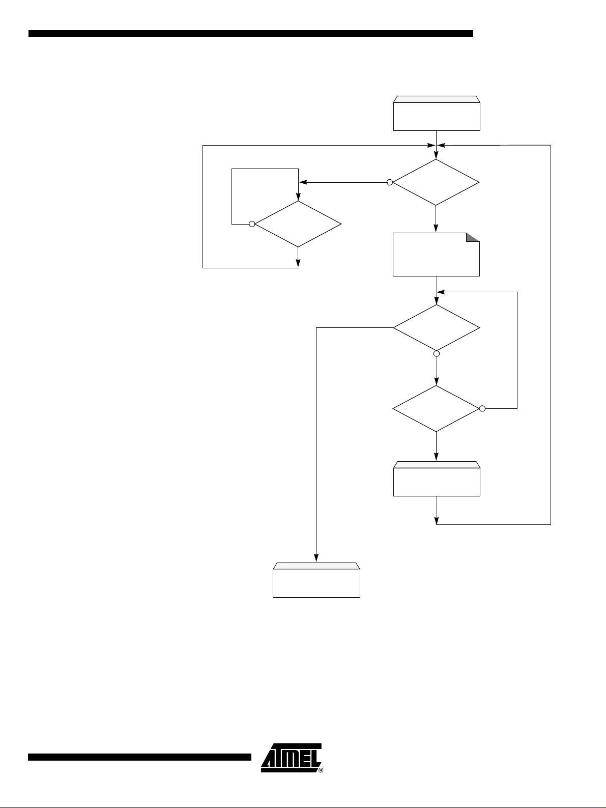
Figure 4. 48 MHz Frequency Auto-generation
AT89C5132
MAIN
No
Resume
Detected?
Yes
No
Yes
USB Connected?
Suspend/Resume
Yes
Configure PLL for
Frequency X
Configure Timer 0
SOF Detected?
No
Timer 0 Overflow?
Yes
No
4256A–USB–06/03
Change Frequency
USB Scheduler
9
Page 10

Protocol
Device Firmware Upgrade Introduction
Device Firmware Upgrade is the mechanism for accomplishing the task of upgrading the
device firmware. Any class of USB device can exploit this capability by supporting the
requirements specified in this document.
Because it is impractical for a device to concurrently perform both DFU operations and
its normal run-time activities, those normal activities must cease for the duration of the
DFU operations. Doing so means that the device must change its operating mode; i.e., a
printer is not
a printer while it is undergoing a firmware upgrade; it is a PROM program-
mer. However, a device that supports DFU is not capable of changing its mode of
operation on its own. External (human or host operating system) intervention is
required.
DFU Specific Requests In addition of the USB standard requests, 7 DFU class-specific requests are employed
to accomplish the upgrade operations, see the following table.
Tab le 4 . DFU Class-specific Requests
bmRequestType bRequest wValue wIndex wLength Data
0010 0001b DFU_DETACH (0) wTimeout Interface (4) Zero none
0010 0001b DFU_DNLOAD (1) wBlock Interface (4) Length Firmware
1010 0001b DFU_UPLOAD (2) wBlock Interface (4) Length Firmware
1010 0001b DFU_GETSTATUS (3) Zero Interface (4) 6 Status
0010 0001b DFU_CLRSTATUS (4) Zero Interface (4) Zero none
1010 0001b DFU_GETSTATE (5) Zero Interface (4) 1 State
0010 0001b DFU_ABORT (6) Zero Interface (4) Zero none
DFU Descriptors set The device exports the DFU descriptor set, which contains:
• A DFU device descriptor
• A single configuration descriptor
• A single interface descriptor (including descriptors for alternate settings, if present)
• A single functional descriptor
DFU Device Descriptor This descriptor is only present in the DFU mode descriptor set. The DFU class code is
reported in the bDeviceClass field of this descriptor.
Tab le 5 . USB Parameters
Parameter ATMEL – AT89C5132 bootloader
Vendor ID 0x03EB
Product ID 0x2FFF
Release Number 0x0000
10
AT89C5132
4256A–USB–06/03
Page 11

Tab le 6 . DFU Mode Device Descriptor
Offset Field Size Value Description
0 bLength 1 12h Size of this descriptor, in bytes
1 bDescriptorType 1 01h DFU FUNCTIONAL descriptor type
AT89C5132
2 bcdUSB 2 0100h
4 bDeviceClass 1 FEh Application Specific Class Code
5 bDeviceSubClass 1 01h Device Firmware Upgrade Code
6 bDeviceProtocol 1 00h
7 bMaxPacketSize0 1 32 Maximum packet size for endpoint zero
8 idVendor 2 03EBh Vendor ID
10 idProduct 2 2FFFh Product ID
12 bcdDevice 2 0x0000 Device release number in binary coded decimal
14 iManufacturer 1 0 Index of string descriptor
15 iProduct 1 0 Index of string descriptor
16 iSerialNumber 1 0 Index of string descriptor
17 bNumConfigurations 1 01h One configuration only for DFU
USB specification release number in binary coded
decimal
The device does not use a class specific protocol on this
interface
DFU Configuration Descriptor This descriptor is identical to the standard configuration descriptor described in the USB
DFU specification version 1.0, with the exception that the bNumInterfaces field must
contain the value 01h.
DFU Interface Descriptor This is the descriptor for the only interface available when operating in DFU mode.
Therefore, the value of the bInterfaceNumber field is always zero.
Tab le 7 . DFU mode Interface Descriptor
Offset Field Size Value Description
0 bLength 1 09h Size of this descriptor, in bytes
1 bDescriptorType 1 04h INTERFACE descriptor type
2 bInterfaceNumber 1 00h Number of this interface
3 bAlternateSetting 1 00h Alternate setting
4 bNumEndpoints 1 00h Only the control pipe is used
5 bInterfaceClass 1 FEh Application Specific Class Code
6 bInterfaceSubClass 1 01h Device Firmware Upgrade Code
7 bInterfaceProtocol 1 00h
8 iInterface 1 00h Index of the String descriptor for this interface
The device doesn’t use a class specific protocol
on this interface
(1)
11
4256A–USB–06/03
Page 12

Note: 1. Alternate settings can be used by an application to access additional memory seg-
ments. In this case, it is suggested that each alternate setting employs a string
descriptor to indicate the target memory segment; e.g., “EEPROM”. Details concerning other possible uses of alternate settings are beyond the scope of this document.
However, their use is intentionally not restricted because it is anticipated that implementers will devise additional creative uses for alternate settings.
DFU Functional Descriptor
Tab le 8 . DFU Functional Descriptor
Offset Field Size Value Description
0 bLength 1 07h Size of this descriptor, in bytes
1 bDescriptorType 1 21h DFU FUNCTIONAL descriptor type
DFU Attributes:
bit 7..3 : reserved
2 bmAttributes 1 Bit mask
3 wDetachTimeOut 2 Number
bit 2: device is able to communicate via USB after Manifestation phase
1 = yes, 0 = no, must see bus reset
bit 1: bitCanUpload : upload capable 1 = yes, 0 = no
bit 0: bitCanDnload : download capable 1 = yes, 0 = no
Time in milliseconds that the device will wait after receipt of the
DFU_DETACH request.
If this time elapses without a USB reset, the device will terminate the
Reconfiguration phase and revert back to normal operation. This
represents the maximum time that the device can wait (depending on its
timers, ...). The Host may specify a shorter timeout in the DFU_DETACH
request.
5 wTransferSize 2 Number
Command Description This protocol allows to:
• Initiate the communication
• Program the Flash Data
• Read the Flash Data
• Program Configuration Information
• Read Configuration and Manufacturer Information
• Erase the Flash
• Start the application
Overview of the protocol is detailed in Appendix-A.
Maximum number of bytes that the device can accept per control-write
transaction
12
AT89C5132
4256A–USB–06/03
Page 13

AT89C5132
Device Status
Get Status The Host employs the DFU_GETSTATUS request to facilitate synchronization with the
device. This status gives information on the execution of the previous request: in
progress/OK/Fail/...
bmRequestType bRequest wValue wIndex wLength Data
1010 0001b DFU_GETSTATUS (3) Zero Interface (4) 6 Status
0010 0001b DFU_CLRSTATUS (4) Zero Interface (4) Zero none
The device responds to the DFU_GETSTATUS request with a payload packet containing the following data:
Tab le 9 . DFU_GETSTATUS Response
Offset Field Size Value Description
0 bStatus 1 Number An indication of the status resulting from the execution of the most recent request.
Minimum time in milliseconds that the host should wait before sending a subsequent
1 bwPollTimeOut 3 Number
4 bState 1 Number
5 iString 1 Index Index of status description in string table.
DFU_GETSTATUS. The purpose of this field is to allow the device to dynamically adjust
the amount of time that the device expects the host to wait between the status phase of
the next DFU_DNLOAD and the subsequent solicitation of the device’s status via
DFU_GETSTATUS.
An indication of the state that the device is going to enter immediately following
transmission of this response.
Tab le 1 0. bStatus Values
Status Value Description
OK 0x00 No error condition is present
errTARGET 0x01 File is not targeted for use by this device
errFILE 0x02 File is for this device but fails some vendor-specific verification test
errWRITE 0x03 Device id unable to write memory
errERASE 0x04 Memory erase function failed
errCHECK_ERASED 0x05 Memory erase check failed
errPROG 0x06 Program memory function failed
errVERIFY 0x07 Programmed memory failed verification
errADDRESS 0x08 Cannot program memory due to received address that is out of range
errNOTDONE 0x09 Received DFU_DNLOAD with wLength = 0, but device does not think it has all the data yet
errFIRMWARE 0x0A Device’s firmware is corrupted. It cannot return to run-time operations
errVENDOR 0x0B iString indicates a vendor-specific error
errUSBR 0x0C Device detected unexpected USB reset signaling
4256A–USB–06/03
13
Page 14

Tab le 1 0. bStatus Values (Continued)
Status Value Description
errPOR 0x0D Device detected unexpected power on reset
errUNKNOWN 0x0E Something went wrong, but the device does not know what it was
errSTALLEDPK 0x0F Device stalled an unexpected request
Tab le 11. bState Values
State Value Description
appIDLE 0 Device is running its normal application
appDETACH 1
dfuIDLE 2 Device is operating in the DFU mode and is waiting for requests
dfuDNLOAD-SYNC 3 Device has received a block and is waiting for the Host to solicit the status via DFU_GETSTATUS
dfuDNBUSY 4 Device is programming a control-write block into its non-volatile memories
dfuDNLOAD-IDLE 5 Device is processing a download operation. Expecting DFU_DNLOAD requests
dfuMANIFEST-SYNC 6
dfuMANIFEST 7 Device is in the Manifestation phase.
dfuMANIFEST-WAIT-RESET 8 Device has programmed its memories and is waiting for a USB reset or a power on reset.
dfuUPLOAD-IDLE 9 The device is processing an upload operation. Expecting DFU_UPLOAD requests.
dfuERROR 10 An error has occurred. Awaiting the DFU_CLRSTATUS request.
Device is running its normal application, has received the DFU_DETACH request, and is waiting for a
USB reset
Device has received the final block of firmware from the Host and is waiting for receipt of
DFU_GETSTATUS to begin the Manifestation phase
or
device has completed the Manifestation phase and is waiting for receipt of DFU_GETSTATUS.
Clear Status Any time the device detects an error and reports an error indication status to the host in
the response to a DFU_GETSTATUS request, it enters the dfuERROR state. The
device cannot transition from the dfuERROR state, after reporting any error status, until
after it has received a DFU_CLRSTATUS request. Upon receipt of DFU_CLRSTATUS,
the device sets a status of OK and transitions to the dfuIDLE state. Only then it is able to
transition to other states.
bmRequestType bRequest wValue wIndex wLength Data
0010 0001b DFU_CLRSTATUS (4) Zero Interface (4) 0 None
Device State This request solicits a report about the state of the device. The state reported is the cur-
rent state of the device with no change in state upon transmission of the response. The
values specified in the bState field are identical to those reported in DFU_GETSTATUS.
bmRequestType bRequest wValue wIndex wLength Data
1010 0001b DFU_GETSTATE (5) Zero Interface (4) 1 State
14
AT89C5132
4256A–USB–06/03
Page 15

AT89C5132
DFU_ABORT Request The DFU_ABORT request enables the device to exit from certain states and return to
the DFU_IDLE state. The device sets the OK status on receipt of this request. For more
information, see the corresponding state transition summary.
bmRequestType bRequest wValue wIndex wLength Data
1010 0001b DFU_ABORT (6) Zero Interface (4) 0 None
Programming the Flash The firmware image is downloaded via control-write transfers initiated by the
DFU_DNLOAD class-specific request. The host sends between bMaxPacketSize0 and
wTransferSize bytes to the device in a control-write transfer. Following each downloaded block, the host solicits the device status with the DFU_GETSTATUS request.
As described in the USB DFU Specification, Firmware images for specific devices are,
by definition, vendor specific. It is therefore required that target addresses, record sizes,
and all other information relative to supporting an upgrade are encapsulated within the
firmware image file. It is the responsibility of the device manufacturer and the firmware
developer to ensure that their devices can consume these encapsulated data. With the
exception of the DFU file suffix, the content of the firmware image file is irrelevant to the
host.
Firmware image:
• 32 bytes: Command
• X bytes: X is the number of byte (00h) added before the first significative byte of the
firmware. The X number is calculated to align the beginning of the firmware with the
flash page. X = start_address [32]. For example, if the start address is 00AFh
(175d), X = 175 [32] = 15.
• The firmware
• The DFU Suffix on 16 Bytes
Tab le 1 2. DFU File Suffix
Offset Field Size Value Description
- 0 dwCRC 4 Number The CRC of the entire file, excluding dwCRC
- 4 bLength 1 16 The length of this DFU suffix including dwCRC
5 : 44h
- 5 ucDfuSignature 3
- 8 bcdDFU 2
- 10 idVendor 2 ID
- 12 idProduct 2 ID
- 14 bcdDevice 2 BCD
6 : 46h
7 : 55h
BCD
0100h
The unique DFU signature field
DFU specification number
The vendor ID associated with this file. Either FFFFh or must match
device’s vendor ID
The product ID associated with this file. Either FFFFf or must match
device’s product ID
The release number of the device associated with this file. Either
FFFFh or a BCD firmware release or version number
4256A–USB–06/03
15
Page 16

Request from Host
Write Command
bmRequestType bRequest wValue wIndex wLength Data
0010 0001b DFU_DNLOAD (1) wBlock Interface (4) Length Firmware
Command Identifier data[0] data[1] data[2] data[3] data[4] Description
Id_prog_start
01h
00h start_address end_address Init Flash programming
The write command is 6 bytes long. In order to reach the USB specification of the Control type transfers, the write command is completed with 26 (=32-6) non-significant
bytes. The total length of the command is then 32 bytes, which is the length of the
Default Control Endpoint.
Firmware The firmware can now be downloaded to the device. In order to be in accordance with
the Flash page size (128 bytes), X non-significant bytes are added before the first byte
to program. The X number is calculated to align the beginning of the firmware with the
Flash page. X = start_address [32]. For example, if the start address is 00AFh (175d), X
= 175 [32] = 15.
DFU Suffix The DFU suffix of 16 bytes are added just after the last byte to program. This suffix is
reserved for future use.
Figure 5. Example of Firmware Download Zero Length DFU_DNLOAD Request
SETUP
OUT
OUT
DFU_DNLOAD
Prog_Start + (EP0 fifo length - 6) x 00h
X offset bytes + Firmware Packet 1
16
OUT
OUT
IN
AT89C5132
Firmware Packet 2
Firmware Packet n + DFU suffix
ZLP
The Host sends a DFU_DNLOAD request with the wLength field cleared to 0 to the
device to indicate that it has completed transferring the firmware image file. This is the
final payload packet of a download operation.
This operation should be preceded by a Long Jump address specification using the corresponding Flash command.
4256A–USB–06/03
Page 17

AT89C5132
Answers from Bootloader After each program request, the Host can request the device state and status by send-
ing a DFU_GETSTATUS message.
If the device status indicates an error, the host can send a DFU_CLRSTATUS request
to the device.
Reading the Flash The flow described below allows the user to read data in the Flash memory. A blank
check command on the Flash memory is possible with this flow.
This operation is performed in 2 steps:
1. DFU_DNLOAD request with the read command (6 bytes)
2. DFU_UPLOAD request which correspond to the immediate previous command.
First Request from Host The Host sends a DFU Download request with a Display command in the data field.
SETUP
OUT
IN
Command
Identifier data[0] data[1] data[2] data[3] data[4] Description
Id_display_data
03h
00h
start_address end_address
01h Blank Check in Flash
DFU_DNLOAD
Display_Data (6 bytes)
ZLP
Display Flash Data
Second Request from Host The Host sends a DFU Upload request.
Answers from the Device The device send to the Host the firmware from the specified start address to the end
address.
SETUP
DFU_UPLOAD
4256A–USB–06/03
IN Firmware Packet 1
IN
IN
OUT
Firmware Packet 2
Firmware Packet n
ZLP
17
Page 18

Answers from the Device to a Blank Check Command
The Host controller send a GET_STATUS request to the device. Once internal blank
check has been completed, the device sends its status.
• If the device status is “OK”:
the device memory is then blank and the device waits the next Host request.
• If the device status is “
the device memory is not blank. The device waits for an DFU_UPLOAD request to
send the first address where the byte is not 0xFF.
errCHECK_ERASED”:
18
AT89C5132
4256A–USB–06/03
Page 19

AT89C5132
Programming Configuration Information
The flow described below allows the user to program Configuration Information regarding the bootloader functionality.
• Boot Process Configuration:
–BSB
–SBV
– Fuse bits (BLJB, X2) (see Section “Mapping and Default Value of Hardware
Security Byte”, page 3)
Ensure that the Program Fuse bit command programs the 4 Fuse bits at the same time.
Request from Host To start the programming operation, the Host sends DFU_DNLOAD request with the
Write command in the data field (6 bytes).
SETUP
OUT
IN
DFU_DNLOAD
Write_command (6 bytes)
ZLP
Command
Identifier data[0] data[1] data[2] data[3] data[4] Description
Id_write_command
04h
00h
01h
02h 00h Value Write value in Fuse (HSB)
01h Write value in SBV
Val ue
05h Write value in SSB
06h Write value in EB
Write value in BSB
Answers from Bootloader The device has two possible answers to a DFU_GETSTATUS request:
• If the chip is protected from program access, a “err_WRITE” status is returned to the
Host.
• Otherwise, the device status is “OK“.
4256A–USB–06/03
19
Page 20

Reading Configuration
Information or Manufacturer
The flow described below allows the user to read the configuration or manufacturer
information.
Information
Requests from Host To start the programming operation, the Host sends DFU_DNLOAD request with the
Read command in the data field (2 bytes).
SETUP
OUT
IN
Command Identifier data[0] data[1] data[2] data[3] data[4] Description
00h Read Bootloader Version
00h
Id_read_command
05h
01h
01h Read Device boot ID1
02h Read Device boot ID2
00h Read BSB
01h Read SBV
05h Read SSB
06h Read EB
30h Read Manufacturer Code
DFU_DNLOAD
Read_command (2 bytes)
ZLP
20
31h Read Family Code
60h Read Product Name
61h Read Product Revision
02h 00h Read HWB
AT89C5132
4256A–USB–06/03
Page 21

AT89C5132
Answers from Bootloader The device has two possible answers to a DFU_GETSTATUS request:
• If the chip is protected from program access, a “err_VENDOR” status is returned to
the Host.
• Otherwise, the device status is “OK“. The Host can send a DFU_UPLOAD request
to the device in order the value of the requested field.
SETUP
IN
OUT
DFU_UPLOAD
Byte value (1 byte)
ZLP
4256A–USB–06/03
21
Page 22

Erasing the Flash The flow described below allows the user to erase the Flash memory.
Two modes of Flash erasing are possible:
• Full chip erase
• Block erase
The Full Chip erase command erases the whole Flash (32 Kbytes) and sets some Configuration Bytes at their default values:
• BSB = FFh
• SBV = FFh
• SSB = FFh (NO_SECURITY)
The Block erase command erases only a part of the Flash.
Four Blocks are defined in the AT89C5132:
• block0 (from 0000h to 1FFFh)
• block1 (from 2000h to 3FFFh)
• block2 (from 4000h to 7FFFh)
• block3 (from 8000h to FFFFh)
Request From Host To start the erasing operation, the Host sends a DFU_DNLOAD request with a Write
Command in the data field (2 bytes).
Command
Identifier data[0] data[1] data[2] data[3] data[4] Description
00h Erase block0 (0K to 8K)
20h Erase block1 (8K to 16K)
Id_write_command
04h
00h
40h Erase block2 (16K to 32K)
80h Erase block3 (32K to 64K)
FFh
Full chip erase (bits at
FFh)
Answers from Bootloader The device has two possible answers to a DFU_GETSTATUS request:
• If the chip is protected from program access, a “err_WRITE” status is returned to the
Host.
• Otherwise, the device status is “OK“.
The full chip erase is always executed whatever the Software Security Byte value is.
22
AT89C5132
4256A–USB–06/03
Page 23

AT89C5132
Starting the Application The flow described below allows to start the application directly from the bootloader
upon a specific command reception.
Two options are possible:
• Start the application with a reset pulse generation (using watchdog).
When the device receives this command the watchdog is enabled and the
bootloader enters a waiting loop until the watchdog resets the device.
Ensure that if an external reset chip is used the reset pulse in output may be wrong
and in this case the reset sequence is not correctly executed.
• Start the application without reset
A jump at the address 0000h is used to start the application without reset.
To start the application, the Host sends a DFU_DNLOAD request with the specified
application start type in the data field (3 or 5 bytes).
This request is immediately followed by a second DFU_DNLOAD request with no data
field to start the application with one of the two options.
Request from Host
SETUP
IN
OUT
SETUP
Command
Identifier data[0] data[1] data[2] data[3] data[4] Description
Id_write_command
04h 03h
00h Hardware reset
01h address – LJMP address
Answer from Bootloader No answer is returned by the device.
DFU_UPLOAD
Jump option (3 or 5 bytes)
ZLP
DFU_UPLOAD
4256A–USB–06/03
23
Page 24

In-Application
Programming/SelfProgramming
The IAP allows to reprogram the microcontroller on-chip Flash memory without removing it from the system and while the embedded application is running.
The user application can call Application Programming Interface (API) routines allowing
IAP. These API are executed by the bootloader.
To call the corresponding API, the user must use a set of Flash_api routines which can
be linked with the application.
Example of Flash_api routines are available on the Atmel web site:
C Flash Drivers for the AT89C5132
The flash_api routines on the package work only with the USB bootloader.
The flash_api routines are listed in APPENDIX-B.
API Call
Process The application selects an API by setting the 4 variables available when the flash_api
library is linked to the application.
These four variables are located in RAM at fixed address:
• api_command: 1Ch
• api_value: 1Dh
• api_dph: 1Eh
• api_dpl: 1Fh
All calls are made through a common interface “USER_CALL” at the address FFF0h.
The jump at the USER_CALL must be done by LCALL instruction to be able to comeback in the application.
Before jump at the USER_CALL, the bit ENBOOT in AUXR1 register must be set.
Constraints The interrupts are not disabled by the bootloader.
Interrupts must be disabled by user prior to jump to the USER_CALL, then re-enabled
when returning.
The user must take care of hardware watchdog before launching a Flash operation.
For more information regarding the Flash writing time see the AT89C5132 datasheet.
24
AT89C5132
4256A–USB–06/03
Page 25

API Commands Several types of APIs are available:
• Read/Program Flash memory
• Read Configuration and Manufacturer Information
• Program Configuration Information
•Erase Flash
• Start bootloader
Read/Program Flash Memory To read the Flash memory the bootloader is not involved.
For more details on these routines see the AT89C5132 Datasheet, section “Program/Code Memory”.
Two routines are available to program the Flash:
– __api_wr_code_byte
– __api_wr_code_page
• The application program load the column latches of the Flash then call the
__api_wr_code_byte or __api_wr_code_page see datasheet, section
“Program/Code Memory
• Parameter settings
”.
AT89C5132
API Name api_command api_dph api_dpl api_value
__api_wr_code_byte
__api_wr_code_page
0Dh – – –
• Instruction: LCALL FFF0h.
Note: No special resources are used by the bootloader during this operation
4256A–USB–06/03
25
Page 26

Read Configuration and Manufacturer Information
• Parameter settings
API Name api_command api_dph api_dpl api_value
__api_rd_HSB 08h – 00h return HSB
__api_rd_BSB 05h – 00h return BSB
__api_rd_SBV 05h – 01h return SBV
__api_rd_SSB 05h – 05h return SSB
__api_rd_EB 05h – 06h return EB
__api_rd_manufacturer 05h – 30h
__api_rd_device_id1 05h – 31h return id1
__api_rd_device_id2 05h – 60h return id2
__api_rd_device_id3 05h – 61h return id3
__api_rd_bootloader_version 0Eh – 00h return value
return
manufacturer id
• Instruction: LCALL FFF0h.
• At the complete API execution by the bootloader, the value to read is in the
api_value variable.
Note: No special resources are used by the bootloader during this operation
26
AT89C5132
4256A–USB–06/03
Page 27

AT89C5132
Program Configuration Information
• Parameter settings
API Name api_command api_dph api_dpl api_value
__api_clr_BLJB 07h – –
__api_set_BLJB 07h – – HSB & BFh
__api_clr_X2 07h – –
__api_set_X2 07h – – HSB & 7Fh
__api_wr_BSB 04h – 00h value to write
__api_wr_SBV 04h – 01h value to write
__api_wr_SSB 04h – 05h value to write
__api_wr_EB 04h – 06h value to write
• instruction: LCALL FFF0h.
Notes: 1. Refer to the AT89C5132 datasheet for information on Write operation Timing.
2. No special resources are used by the bootloader during these operations.
Erasing the Flash The AT89C5132 Flash memory is divided into four blocks:
Block 0: from address 0000h to 1FFFh (64 pages)
(HSB & BFh) |
40h
(HSB & 7Fh) |
80h
Block 1: from address 2000h to 3FFFh (64 pages)
Block 2: from address 4000h to 7FFFh (128 pages)
Block 3: from address 8000h to FFFFh (256 pages)
• Parameter settings
API Name api_command api_dph api_dpl api_value
__api_erase_block0 00h 00h – –
__api_erase_block1 00h 20h –
__api_erase_block2 00h 40h –
__api_erase_block3 00h 80h –
• Instruction: LCALL FFF0h.
Note: 1. Refer to the AT89C5132 datasheet for information on Write operation Timing, then
multiply this timing by the number of pages.
2. No special resources are used by the bootloader during these operations.
Starting the Bootloader This routine allows to start at the beginning of the bootloader as after a reset. After call-
ing this routine the regular boot process is performed and the communication must be
opened before any action.
• No special parameter setting
• Set bit ENBOOT in AUXR1 register
• instruction: LJUMP or LCALL at address F000h
4256A–USB–06/03
27
Page 28

Appendix-A Table 13. Summary of Frames from Host
Command Identifier data[0] data[1] data[2] data[3] data[4] Description
Id_prog_start
01h
Id_display_data
03h
Id_write_command
04h
00h start_address end_address Init Flash programming
00h
01h Blank Check in Flash
00h
01h
02h 00h
03h
start_address end_address
00h Erase block0 (0K to 8K)
20h Erase block1 (8K to 16K)
40h Erase block2 (16K to 32K)
80h Erase block3 (32K to 64K)
FFh
00h
01h Write value in SBV
Val ue
05h Write value in SSB
06h Write value in EB
Val ue
00h Hardware reset
01h address – LJMP address
Display Flash Data
Full chip erase (bits at
FFh)
Write value in BSB
Write value in Fuse (HSB)
Id_read_command
05h
00h – – – Read Bootloader version
00h
01h
02h 00h Read HWB
01h – – – Read Device boot ID1
02h – – – Read Device boot ID2
00h Read BSB
01h Read SBV
05h Read SSB
06h Read EB
30h Read Manufacturer Code
31h Read Family Code
60h Read Product Name
61h Read Product Revision
28
AT89C5132
4256A–USB–06/03
Page 29

AT89C5132
Tab le 1 4. DFU Class-specific Requests
bmRequestType bRequest wValue wIndex wLength Data
0010 0001b DFU_DETACH (0) wTimeout Interface (4) Zero none
0010 0001b DFU_DNLOAD (1) wBlock Interface (4) Length Firmware
1010 0001b DFU_UPLOAD (2) wBlock Interface (4) Length Firmware
1010 0001b DFU_GETSTATUS (3) Zero Interface (4) 6 Status
0010 0001b DFU_CLRSTATUS (4) Zero Interface (4) Zero none
1010 0001b DFU_GETSTATE (5) Zero Interface (4) 1 State
0010 0001b DFU_ABORT (6) Zero Interface (4) Zero none
Tab le 1 5. USB Parameters
Parameter ATMEL
Vendor ID 0x03EB
Product ID 0x2FFF
Release Number 0x0000
Tab le 1 6. Hardware Security Byte (HSB)
76543210
X2 BLJB –––LB2 LB1 LB0
4256A–USB–06/03
29
Page 30

Appendix-B
Tab le 1 7. API Summary
Function Name
__api_rd_code_byte no
__api_wr_code_byte yes 0Dh – – –
__api_wr_code_page yes 0Dh – – –
__api_erase block0 yes 00h 00h – –
__api_erase block1 yes 00h 20h – –
__api_erase block2 yes 00h 40h – –
__api_erase block3 yes 00h 80h – –
__api_rd_HSB yes 08h – 00h return value
__api_clr_BLJB yes 07h – – (HSB & BFh) | 40h
__api_set_BLJB yes 07h – – HSB & BFh
__api_clr_X2 yes 07h – – (HSB & 7Fh) | 80h
__api_set_X2 yes 07h – – HSB & 7Fh
__api_rd_BSB yes 05h – 00h return value
Bootloader
Execution api_command api_dph api_dpl api_value
__api_wr_BSB yes 04h – 00h value
__api_rd_SBV yes 05h – 01h return value
__api_wr_SBV yes 04h – 01h value
__api_erase_SBV yes 04h – 01h FFh
__api_rd_SSB yes 05h – 05h return value
__api_wr_SSB yes 04h – 05h value
__api_rd_EB yes 05h – 06h return value
__api_wr_EB yes 04h – 06h value
__api_rd_manufacturer yes 05h – 30h return value
__api_rd_device_id1 yes 05h – 31h return value
__api_rd_device_id2 yes 05h – 60h return value
__api_rd_device_id3 yes 05h – 61h return value
__api_rd_bootloader_version yes 0Eh – 00h return value
__api_start_bootloader no – – – –
__api_start_isp no – – – –
30
AT89C5132
4256A–USB–06/03
Page 31

Atmel Corporation Atmel Operations
2325 Orchard Parkway
San Jose, CA 95131
Tel: 1(408) 441-0311
Fax: 1(408) 487-2600
Regional Headquarters
Europe
Atmel Sarl
Route des Arsenaux 41
Case Postale 80
CH-1705 Fribourg
Switzerland
Tel: (41) 26-426-5555
Fax: (41) 26-426-5500
Asia
Room 1219
Chinachem Golden Plaza
77 Mody Road Tsimshatsui
East Kowloon
Hong Kong
Tel: (852) 2721-9778
Fax: (852) 2722-1369
Japan
9F, Tonetsu Shinkawa Bldg.
1-24-8 Shinkawa
Chuo-ku, Tokyo 104-0033
Japan
Tel: (81) 3-3523-3551
Fax: (81) 3-3523-7581
Memory
2325 Orchard Parkway
San Jose, CA 95131
Tel: 1(408) 441-0311
Fax: 1(408) 436-4314
Microcontrollers
2325 Orchard Parkway
San Jose, CA 95131
Tel: 1(408) 441-0311
Fax: 1(408) 436-4314
La Chantrerie
BP 70602
44306 Nantes Cedex 3, France
Tel: (33) 2-40-18-18-18
Fax: (33) 2-40-18-19-60
ASIC/ASSP/Smart Cards
Zone Industrielle
13106 Rousset Cedex, France
Tel: (33) 4-42-53-60-00
Fax: (33) 4-42-53-60-01
1150 East Cheyenne Mtn. Blvd.
Colorado Springs, CO 80906
Tel: 1(719) 576-3300
Fax: 1(719) 540-1759
Scottish Enterprise Technology Park
Maxwell Building
East Kilbride G75 0QR, Scotland
Tel: (44) 1355-803-000
Fax: (44) 1355-242-743
RF/Automotive
Theresienstrasse 2
Postfach 3535
74025 Heilbronn, Germany
Tel: (49) 71-31-67-0
Fax: (49) 71-31-67-2340
1150 East Cheyenne Mtn. Blvd.
Colorado Springs, CO 80906
Tel: 1(719) 576-3300
Fax: 1(719) 540-1759
Biometrics/Imaging/Hi-Rel MPU/
High Speed Converters/RF Datacom
Avenue de Rochepleine
BP 123
38521 Saint-Egreve Cedex, France
Tel: (33) 4-76-58-30-00
Fax: (33) 4-76-58-34-80
e-mail
literature@atmel.com
Web Site
http://www.atmel.com
Disclaimer: Atmel Corporation makes no warranty for the use of its products, other than those expressly contained in the Company’s standard
warranty which is detailed in Atmel’s Terms and Conditions located on the Company’s web site. The Company assumes no responsibility for any
errors which may appear in this document, reserves the right to change devices or specifications detailed herein at any time without notice, and
does not make any commitment to update the information contained herein. No licenses to patents or other intellectual property of Atmel are
granted by the Company in connection with the sale of Atmel products, expressly or by implication. Atmel’s products are not authorized for use
as critical components in life support devices or systems.
© Atmel Corporation 2003. All rights reserved. Atmel® and combinations thereof are the registered
trademarks of Atmel Corporation or its subsidiaries. Other terms and product names may be the trademarks of
others.
Printed on recycled paper.
4256A–USB–06/03
/xM
 Loading...