

Page 1

Features
• 80C52X2 Core (6 Clocks per Instruction)
– Maximum Core Frequency 40 MHz in X1 Mode
– Dual Data Pointer
– Full-duplex Enhanced UART (EUART)
– Three 16-bit Timer/Counters: T0, T1 and T2
– 256 Bytes of Scratchpad RAM
• 32-Kbyte On-chip Flash In-System Programming through USB or UART
• 4-Kbyte EEPROM for Boot (3-Kbyte) and Data (1-Kbyte)
• On-chip Expanded RAM (XRAM): 1024 Bytes
• USB Module with Interrupt on Transfer Completion
– Endpoint 0 for Control Transfers: 32-byte FIFO
– 6 Programmable Endpoints with In or Out Directions and with Bulk, Interrupt or
Isochronous Transfers
• Endpoint 1, 2, 3: 32-byte FIFO
• Endpoint 4, 5: 2 x 64-byte FIFO with Double Buffering (Ping-pong Mode)
• Endpoint 6: 2 x 512-byte FIFO with Double Buffering (Ping-pong Mode)
– Suspend/Resume Interrupts
– Power-on Reset and USB Bus Reset
– 48 MHz DPLL for Full-speed Bus Operation
– USB Bus Disconnection on Microcontroller Request
• 5 Channels Programmable Counter Array (PCA) with 16-bit Counter, High-speed
Output, Compare/Capture, PWM and Watchdog Timer Capabilities
• Programmable Hardware W atchdog T imer (One-time Ena bled with Reset-out): 50 ms to
6s at 4 MHz
• Keyboard Interrupt Interface on Port P1 (8 Bits)
• SPI Interface (Master/Slave Mode)
• 34 I/O Pins
• 4 Direct-drive LED Outputs with Programmable Current Sources: 2-6-10 mA Typical
• 4-level Priority Interrupt System (11 sources)
• Idle and Power-down Modes
• 0 to 32 MHz On-chip Oscillator with Analog PLL for 48 MHz Synthesis
• Voltage Regulator and Reference Output: 3.3V/4 mA
• Low Power Voltage Range
– 3.0V to 3.6V
– 30 mA Max Operating Current (at 40 MHz)
– 100 µA Max Power-d own Current
• Self-powered USB Voltage Range (Not Available on First Version)
– 3.6V to 5.5V
– 30 mA Max Operating Current (at 40 MHz)
– 200 µA Max Power-d own Current
• Commercial and Industrial Temperature Range
• Packages: PLCC52, VQFP64, MLF48, SO28
8-bit Flash
Microcontroller
with Full Speed
USB Device
AT89C5131
Rev. 4136A–USB–03/03
Page 2

Description AT89C5131 is a high-performance Flash version of the 80C51 single-chip 8-bit micro-
controllers with full speed USB functions.
AT89C5131 features a full-speed USB module compatible with the USB specifications
Version 1.1 and 2.0. This module integrates the USB transceivers with a 3.3V voltage
regulator and the Serial Interface Engine (SIE) with Digital Phase Locked Loop and
48 MHz clock recovery. USB Event detection logic (Reset and Suspend/Resume) and
FIFO buffers supporting the mandatory control Endpoint (EP0) and up to 6 versatile
Endpoints (EP1/EP2/EP3/EP4/EP5/EP6) with minimum software overhead are also part
of the USB module.
AT89C5131 retains the features of the Atmel 80C52 with extended Flash capacity (32Kbyte), 256 bytes of intern al RAM, a 4-level in terrup t system , two 16- bit timer /coun ters
(T0/T1), a full duplex enhanced UART (EUART) and an on-chip oscillator.
In addition, AT89C 5131 has a n on-chip e xpanded RAM of 1024 bytes (XRAM) , a dualdata pointer, a 16-bi t up/do wn Timer (T2), a Prog ramma ble Counte r Arr ay (PCA ), up to
4 programmable LED current sources, a programmable hardware watchdog and a
power-on reset.
AT89C5131 has tw o soft war e- sele cta bl e m ode s of r e duc ed ac tivi ty for fu rther r ed uct io n
in power consumption . In the id le mode th e CPU is fr ozen while th e timers, th e serial
ports and the interrupt system are still operating. In the power-down mode the RAM is
saved, the peripheral clock is frozen, but the dev ice has full wake- up capabil ity through
USB events or external interrupts.
2
AT89C5131
4136A–USB–03/03
Page 3
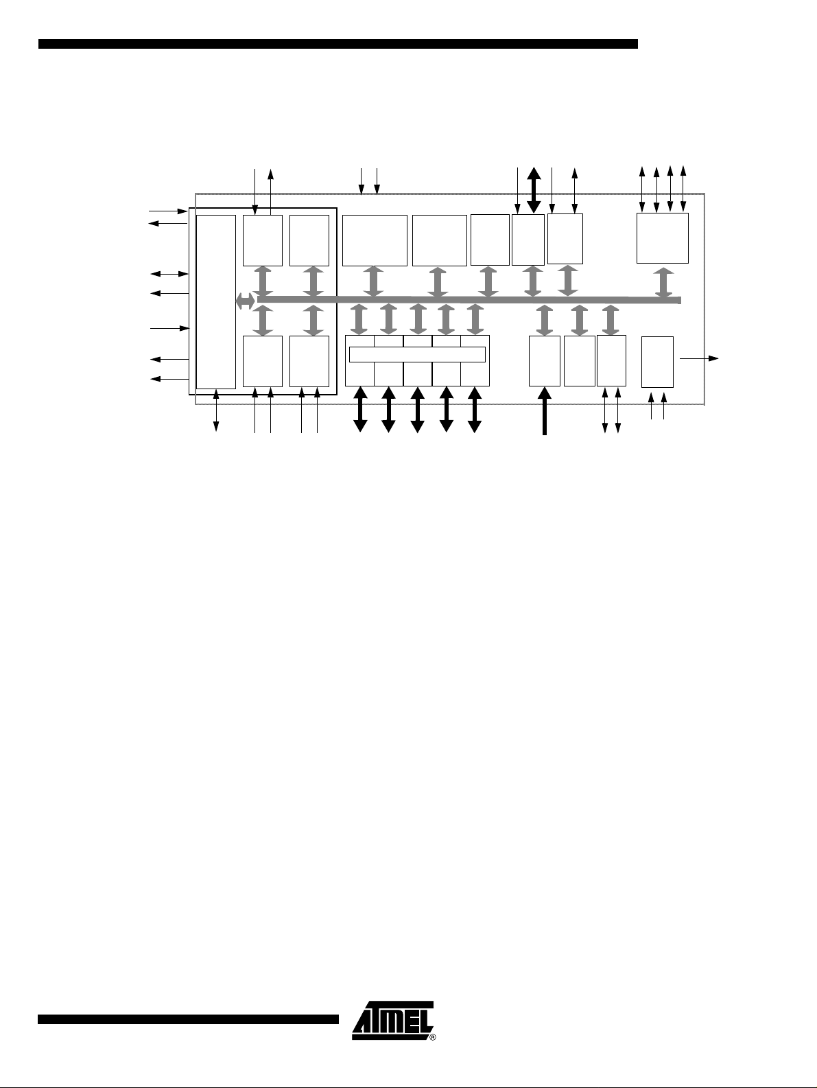
Block Diagram
XTAL1
XTAL2
ALE
PSEN
EA
CPU
RxD
(2)(2)
EUART
+
BRG
TxD
C51
CORE
RAM
256x8
VDD
VSS
32Kx8 Flash
EEPROM
4Kx8
XRAM
1Kx8
ECI
(1)(1)
PCA
CEX
T2EX
(1)
(1)
Timer2
T2
AT89C5131
SS
MISO
MOSI
SCK
(1) (1) (1)
(1)
SPI
(2)
RD
(2)
WR
RST
Notes: 1. Alternate function of Port 1
2. Alternate function of Port 3
3. Alternate function of Port 4 (Alternate function of Port 4 on PLCC52, under evaluation)
Timer 0
Timer 1
(2) (2) (2) (2)
T0
T1
INT
Ctrl
INT0
Parallel I/O Ports & Ext. Bus
Port 0
Port 1
P1
INT1
P0
Port 2
P2
Port 3
P3
Port 4
P4
Key
Board
KIN
Watch
Dog
USB
D -
D +
Regu-
lator
AVSS
VREF
AVDD
4136A–USB–03/03
3
Page 4
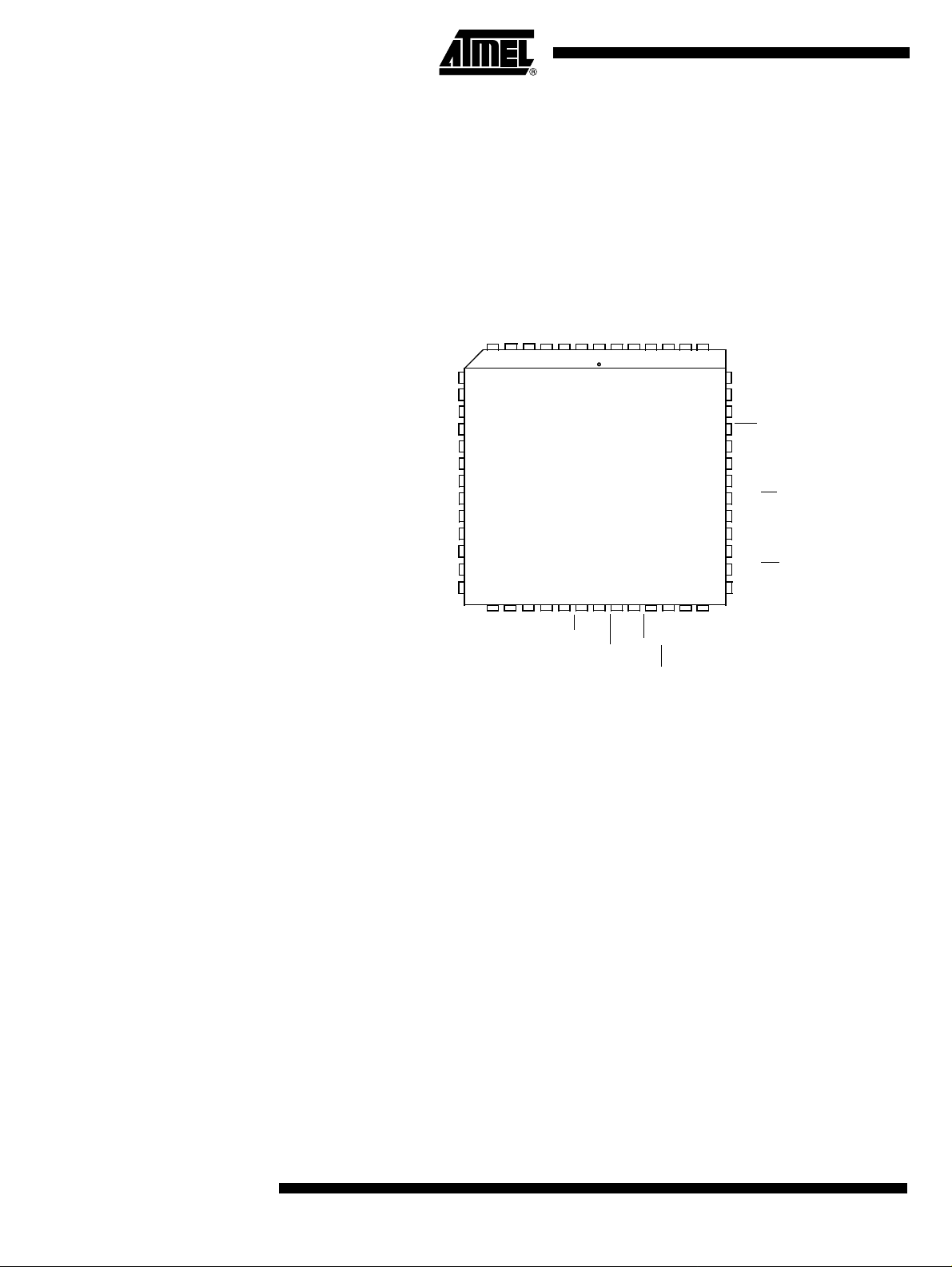
Pinout Description
Pinout
Figure 1. AT89C5131 52-pin PLCC Pinout
P4.0
P1.7/CEX4/KIN7/MOSI
P1.6/CEX3/KIN6/SCK
P2.2/A10
P1.5/CEX2/KIN5/MISO
5 4 3 2 1 6
7 47
P4.1
8
VDD
AVDD
NC
AVSS
9
10
11
12
13
14
15
16
17
18
19
20
2122 26252423 292827 30 31
D-
PLLF
D+
PLCC52
NC
VREF
P2.3/A11
P2.4/A12
P2.5/A13
XTAL2
XTAL1
P2.6/A14
P2.7/A15
P3.0/RxD
P2.0/A8
P2.1/A9
P0.0/AD0
52 51 50 49 48
EA
ALE
PSEN
P1.4/CEX1/KIN4
P3.1/TxD
P1.3/CEX0/KIN3
P3.2/INT0
P1.2/ECI/KIN2
32 33
/LED0
P3.3/INT1
P1.1/T2EX/KIN1/SS
P3.4/T0
P1.0/T2/KIN0
NC
46
P0.1/AD1
45
P0.2/AD2
44
43
RST
42
P0.3/AD3
VSS
41
P0.4/AD4
40
39
P3.7/RD/LED3
P0.5/AD5
38
37
P0.6/AD6
36
P0.7/AD7
35
P3.6/WR/LED2
NC
34
P3.5/T1/LED1
4
AT89C5131
4136A–USB–03/03
Page 5
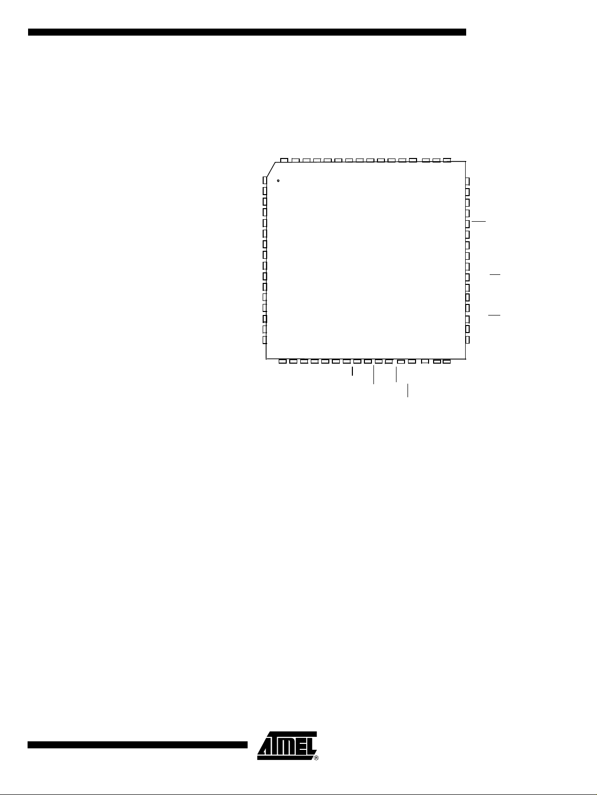
Figure 2. AT89C5131 64-pin VQFP Pinout
P4.0
NC
P2.3/A11
P2.4/A12
P2.5/A13
XTAL2
XTAL1
P2.6/A14
P2.7/A15
VDD
AVDD
NC
AVSS
NC
P3.0/RxD
NC
NC
NC
P4.1
64
1
2
3
4
5
6
7
8
9
10
11
12
13
14
15
16
P1.6/CEX3/KIN6/SCK
P1.7/CEX4/KIN7/MOSI
62 61 60 59 58 63
17 18 22212019 252423 26 27
P2.1/A9
P2.2/A10
P1.5/CEX2/KIN5/MISO
57 56 55 54 53
VQFP64
AT89C5131
P2.0/A8
P0.0/AD0
P1.4/CEX1/KIN4
28
P1.3/CEX0/KIN3
29
52
P1.2/ECI/KIN2
51 50
30
P1.1/T2EX/KIN1/SS
31 32
P1.0/T2/KIN0
NC
49
48
47
46
45
44
43
42
41
40
39
38
37
36
35
34
33
NC
NC
P0.1/AD1
P0.2/AD2
RST
P0.3/AD3
VSS
NC
P0.4/AD4
P3.7/RD/LED3
P0.5/AD5
P0.6/AD6
P0.7/AD7
P3.6/WR/LED2
NC
NC
NC
NC
PLLF
D-
D+
NC
EA
ALE
VREF
PSEN
/LED0
P3.1/TxD
P3.2/INT0
P3.3/INT1
NC
P3.4/T0
P3.5/T1/LED1
4136A–USB–03/03
5
Page 6
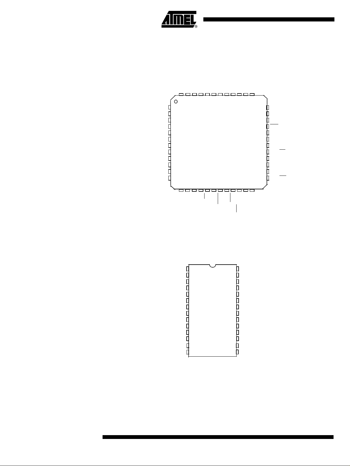
Figure 3. AT89C5131 48-pin MLF Pinout
P4.0
P1.7/CEX4/KIN7/MOSI
P1.6/CEX3/KIN6/SCK
P1.5/CEX2/KIN5/MISO
P2.2/A10
46 45 44 43 42 47
48
1
P4.1
XTAL2
XTAL1
VDD
AVDD
AVSS
2
3
4
5
6
7
8
9
10
11
12
MLF 48
1314 18171615 212019 22 23
D-
D+
EA
PLLF
VREF
P2.3/A11
P2.4/A12
P2.5/A13
P2.6/A14
P2.7/A15
P3.0/RxD
P2.0/A8
P2.1/A9
P0.0/AD0
41 40 39 38 37
ALE
PSEN
P3.1/TxD
P1.4/CEX1/KIN4
P3.2/INT0
P1.3/CEX0/KIN3
/LED0
P3.3/INT1
P1.2/ECI/KIN2
P3.4/T0
24
P1.1/T2EX/KIN1/SS
25
P3.5/T1/LED1
P1.0/T2/KIN0
36
P0.1/AD1
35
P0.2/AD2
34
33
RST
32
P0.3/AD3
31
VSS
P0.4/AD4
30
29
P3.7/RD/LED3
P0.5/AD5
28
27
P0.6/AD6
P0.7/AD7
26
P3.6/WR/LED2
Figure 4. AT89C5131 28-pin SO Pinout
P1.5/CEX2/KIN5/MISO
P1.6/CEX3/KIN6/SCK
P1.7/CEX4/KIN7/MOSI
P3.0/RxD
1
2
3
P4.0
4
P4.1
5
XTAL2
XTAL1
VDD
AVSS
PLLF
D-
D+
VREF P3.1/TxD
SO28
6
7
8
9
10
11
12
13
14
28
P1.4/CEX1/KIN4
P1.3/CEX0/KIN3
27
26
P1.2/ECI/KIN2
25
P1.1/T2EX/KIN1/SS
P1.0/T2/KIN0
24
23
RST
VSS
22
21
P3.7/RD/LED3
P3.6/WR/LED2
20
P3.5/T1/LED1
19
P3.4/T0
18
P3.3/INT1/LED0
17
P3.2/INT0
16
15
6
AT89C5131
4136A–USB–03/03
Page 7

AT89C5131
Signals All the AT89C5131 signals are detailed by functionality on Table 1 through Table 11.
Table 1. Keypad Interface Signal Description
Signal
Name Type Description
Alternate
Function
KIN[7:0) I
Keypad Input Lines
Holding one of these pins high or low for 24 oscillator periods triggers a
keypad interrupt if enabled. Held line is reported in the KBCON register.
Table 2. Programmable Counter Array Signal Description
Signal
Name Type Description
ECI I External Clock Input P1.2
Capture External Input
CEX[4:0] I/O
Compare External Output
Table 3. Serial I/O Signal Description
Signal
Name Type Description
Serial Input
RxD I
TxD O
The serial input is P3.0 after reset, but it can also be configured to P4.0 by
software.
Serial Output
The serial output is P3.1 after reset, but it can also be configured to P4.1 by
software.
P1[7:0]
Alternate
Function
P1.3
P1.4
P1.5
P1.6
P1.7
Alternate
Function
P3.0
P3.1
4136A–USB–03/03
Table 4. Timer 0, Timer 1 and Timer 2 Signal Description
Signal
Name Type Description
Timer 0 Gate Input
INT0
serves as external run control for timer 0, when selected by GATE0
bit in TCON register.
INT0 I
INT1 I
External Interrupt 0
input set IE0 in the TCON register. If bit IT0 in this register is set, bits
INT0
IE0 are set by a falling edge on INT0
a low level on INT0
Timer 1 Gate Input
serves as external run control for Timer 1, when selected by GATE1
INT1
bit in TCON register.
External Interrupt 1
input set IE1 in the TCON register. If bit IT1 in this register is set, bits
INT1
IE1 are set by a falling edge on INT1
a low level on INT1
.
.
. If bit IT0 is cleared, bits IE0 is set by
. If bit IT1 is cleared, bits IE1 is set by
Alternate
Function
P3.2
P3.3
7
Page 8

Table 4. Timer 0, Timer 1 and Timer 2 Signal Description (Continued)
Signal
Name Type Description
Alternate
Function
T0 I
T1 I
T2
T2EX I Timer/Counter 2 Reload/Capture/Direction Control Input P1.1
Timer Counter 0 External Clock Input
When Timer 0 operates as a counter, a falling edge on the T0 pin
increments the count.
Timer/Counter 1 External Clock Input
When Timer 1 operates as a counter, a falling edge on the T1 pin
increments the count.
IOTimer/Counter 2 External Clock Input
Timer/Counter 2 Clock Output
Table 5. LED Signal Description
Signal
Name Ty p e Description
Direct Drive LED Output
LED[3:0] O
These pins can be directly connected to the Cathode of standard LEDs
without external current limiting resistors. The typical current of each
output can be programmed by software to 2, 6 or 10 mA. Several outputs
can be connected together to get higher drive capabilities.
Table 6. SPI Signa l De scr ip tion
Signal
Name Type Description
P3.4
P3.5
P1.0
Alternate
Function
P3.3
P3.5
P3.6
P3.7
Alternate
Function
SS I/O SS
MISO I/O
SCK I/O
MOSI
I/O
: SPI Slave Select P1.1
MISO: SPI Master Input Slave Output line
When SPI is in master mode, MISO receives data from the slave
peripheral. When SPI is in slave mode, MISO outputs data to the master
controller.
SCK: SPI Serial Clo ck
SCK outputs clock to the slave peripheral or receive clock from the master
MOSI: SPI Master Output Slave Input line
When SPI is in master mode, MOSI outputs data to the slave peripheral.
When SPI is in slave mode, MOSI receives data from the master controller
P1.5
P1.6
P1.7
8
AT89C5131
4136A–USB–03/03
Page 9
AT89C5131
Table 7. Ports Signal Description
Signal
Name Type Description Alternate Function
Port 0
P0 is an 8-bit open-drain bidirectional I/O port. Port 0
P0[7:0] I/O
P1[7:0] I/O
pins that have 1s written to them float and can be used
as high impedance inputs. To avoid any parasitic current
consumption, Floating P0 inputs must be pulled to V
.
V
SS
Port 1
P1 is an 8-bit bidirectional I/O port with internal pull-ups,
except for P1.6 and P1.7 that are true open drain
outputs.
DD
or
AD[7:0]
KIN[7:0]
T2
T2EX
ECI
CEX[4:0]
P2[7:0] I/O
P3[7:0] I/O
P4[1:0] I/O
Port 2
P2 is an 8-bit bidirectional I/O port with internal pull-ups.
Port 3
P3 is an 8-bit bidirectional I/O port with internal pull-ups.
Port 4
P4 is an 2-bit bidirectional I/O port.
Table 8. Clock Signal Description
Signal
Name Type Description
XTAL1 I
XTAL2 O
Input to the on-chip inv e r ting oscillator amplifie r
To use the internal oscillator, a crystal/resonator circuit is connected to this
pin. If an external oscillator is used, its output is connected to this pin.
Output of the on-chip inverting oscillator amplifier
To use the internal oscillator, a crystal/resonator circuit is connected to this
pin. If an external oscillator is used, leave XTAL2 uncon nected.
A[15:8]
LED[3:0]
RxD
TxD
INT0
INT1
T0
T1
WR
RD
Alternate
Function
-
-
4136A–USB–03/03
PLLF I
PLL Low Pass Filter input
Receives the RC network of the PLL low pass filter.
Table 9. USB Signa l Desc ript ion
Signal
Name Type Description
D+ I/O USB Data + signal -
D- I/O USB Data - signal -
VREF O
USB Reference Voltage
Connect this pin to D+ using a 1.5 kΩ resistor to use the Detach function.
-
Alternate
Function
-
9
Page 10

Table 10. System Signal Description
Signal
Name Type Description
Alternate
Function
AD[7:0] I/O
A[15:8] I/O
RD I/O
WR I/O
RST I
ALE O
Multiplexed Address/Data LSB for external access
Data LSB for Slave port access (used for 8-bit and 16-bit modes)
Address Bus MSB for external access
Data MSB for Slave port access (used for 16-bit mode only)
Read Signal
Read signal asserted during external data memory read operation.
Control input for slave port read access cycles.
Write Signal
Write signal asserted during external data memory write operation.
Control input for slave write access cycles.
Reset Input
Holding this pin low for 64 oscillator periods while the oscillator is running
resets the device. The Port pins are driven to their reset conditions when a
voltage lower than V
This pin has an internal pull-up resistor which allows the device to be reset
by connecting a capacitor between this pin and VSS.
Asserting RST
the chip to normal operation.
This pin is set to 0 for at least 12 oscillator periods when an internal reset
occurs.
Address Latch Enable Output
The falling edge of ALE strobes the address into external latch. This signal
is active only when reading or writing external memory using MOVX
instructions.
is applied, whether or not the oscillator is running.
IL
when the chip is in Idle mode or Power-down mode returns
P0[7:0]
P2[7:0]
P3.7
P3.6
-
-
PSEN O
EA I
Program
Test mode entry signal. This pin must be set to V
External Access Enable
This pin must be held low to force the device to fetch code from external
program memory starting at address 0000h. It is latched during reset and
cannot be dynamically changed during operation.
Table 11. Power Signal Description
Signal
Name Type Description
AVSS GND
AVDD PWR
VSS GND
VDD PWR
Alternate Ground
AVSS is used to supply the on-chip PLL.
Alternate Ground
AVDD is used to supply the on-chip PLL.
Digital Ground
VSS is used to supply the buffer ring and the digital core.
Digital Supply Voltage
VDD is used to supply the buffer ring on all versions of the device.
It is also used to power the on-chip voltage regulator of the Standard
versions or the digital core of the Low Power versions.
for normal operation.
DD
-
-
Alternate
Function
-
-
-
-
10
AT89C5131
4136A–USB–03/03
Page 11

Table 11. Power Signal Description (Continued)
Signal
Name Type Description
3V Voltag e Reference
VREF is used to supply the on-chip USB differential drivers.
VREF PWR
It is internally connected to the on-chip voltage regulator output of the
standard versions, which must be connected to an external decoupling
capacitor and can be connected to D+ with a 15 kΩ resistor.
It must be provided from outside on the Low Power versions, which have
no internal voltage regulator.
AT89C5131
Alternate
Function
-
4136A–USB–03/03
11
Page 12

SFR Mapping The Special Function Registers (SFRs) of the AT89C5131 fall into the following
categories:
• C51 core registers: ACC, B, DPH, DPL, PSW, SP
• I/O port registers: P0, P1, P2, P3, P4
• Timer registers: T2CON, T2MOD, TCON, TH0, TH1, TH2, TMOD, TL0, TL1, TL2,
RCAP2L, RCAP2H
• Serial I/O port registers: SADDR, SADEN, SBUF, SCON
• PCA (Programmable Counter Array) registers: CCON, CMOD, CCAPMx, CL, CH,
CCAPxH, CCAPxL (x: 0 to 4)
• Power and clock control registers: PCON
• Hardware Watchdog Timer registers: WDTRST, WDTPRG
• Interrupt system registers: IE0, IPL0, IPH0, IE1, IPL1, IPH1
• Keyboard Interface registers: KBE, KBF, KBLS
• LED register: LEDCON
• Serial Port Interface (SPI) registers: SPCON, SPSTA, SPDAT
• USB registers: Uxxx (17 registers)
• PLL registers: PLLCON, PLLDIV0
• BRG (Baud Rate Generator) registers: BRL, BDRCON
• Flash register: FCON (FCON access is reserved for the Flash API and ISP
software)
• EEPROM register: EECON
• Clock Prescaler register: CKRL
• 32 kHz Sub Clock Oscillator registers: CKSEL
• Others: AUXR, AUXR1, CKCON0, CKCON1
12
AT89C5131
4136A–USB–03/03
Page 13

Table 12. SFR Descriptions
Reserved
Bit
Addressable Non-Bit Addressable
0/8 1/9 2/A 3/B 4/C 5/D 6/E 7/F
AT89C5131
The table below shows all SFRs with their address and their reset value.
F8h
F0h
E8h
E0h
D8h
D0h
C8h
C0h
B8h
B0h
UEPINT
0000 0000
B
0000 0000
ACC
0000 0000
CCON
00X0 0000
PSW
0000 0000
T2CON
0000 0000
P4
X XXX 1111
IPL0
X000 000
P3
1111 1111
CH
0000 0000
LEDCON
0000 0000
CL
0000 0000
CMOD
00XX X000
FCON (1)
XXXX 0000
T2MOD
XXXX XX00
SADEN
0000 0000
IE1
XXXX X000
CCAP0H
XXXX XXXX
CCAP0L
XXXX XXXX
UBYCTLX
0000 0000
CCAPM0
X000 0000
EECON
0000 0000
RCAP2L
0000 0000
UEPIEN
0000 0000
UFNUML
0000 0000
IPL1
XXXX X000
CCAP1H
XXXX XXXX
CCAP1L
XXXX XXXX
UBYCTHX
0000 0000
CCAPM1
X000 0000
RCAP2H
0000 0000
SPCON
0001 0100
UFNUMH
0000 0000
IPH1
XXXX X111
CCAP2H
XXXX XXXX
CCAP2L
XXXX XXXX
CCAPM2
X000 0000
UEPCONX
1000 0000
TL2
0000 0000
SPSTA
0000 0000
USBCON
0000 0000
CCAP3H
XXXX XXXX
CCAP3L
XXXX XXXX
CCAPM3
X000 0000
UEPRST
0000 0000
TH2
0000 0000
SPDAT
XXXX XXXX
USBINT
0000 0000
CCAP4H
XXXX XXXX
CCAP4L
XXXX XXXX
CCAPM4
X000 0000
UDPADDL
0000 0000
UEPSTAX
0000 0000
USBADDR
0000 0000
USBIEN
0000 0000
UDPADDH
0000 0000
UEPDATX
0000 0000
UEPNUM
0000 0000
IPH0
X000 0000
FFh
F7h
EFh
E7h
DFh
D7h
CFh
C7h
BFh
B7h
A8h
A0h
98h
90h
88h
80h
IE0
0000 0000
P2
1111 1111
SCON
0000 0000
P1
1111 1111
TCON
0000 0000
P0
1111 1111
0/8 1/9 2/A 3/ B 4/C 5/D 6/E 7/F
SADDR
0000 0000
SBUF
XXXX XXXX
TMOD
0000 0000
SP
0000 0111
AUXR1
XXXX X0X0
BRL
0000 0000
TL0
0000 0000
DPL
0000 0000
PLLCON
XXXX XX00
BDRCON
XXX0 0000
TL1
0000 0000
DPH
0000 0000
PLLDIV0
0000 0000
0000 0000
0000 0000
Note: 1. FCON access is reserved for the Flash API and ISP software.
KBLS
TH0
KBE
0000 0000
TH1
0000 0000
WDTRST
XXXX XXXX
KBF
0000 0000
AUXR
XX0X 0000
CKCON1
0000 0000
WDTPRG
XXXX X000
CKCON0
0000 0000
PCON
00X1 0000
AFh
A7h
9Fh
97h
8Fh
87h
4136A–USB–03/03
13
Page 14

The Special Function Registers (SFRs) of the AT89C5131 fall into the following
categories:
Table 13. C51 Core SFRs
MnemonicAddName 76543210
ACC E0h Accumulator
B F0h B Register
PSW D0h
SP 81h
DPL 82h
DPH 83h
Program Status
Word
Stack Po in ter
LSB of SPX
Data Pointer
Low byte
LSB of DPTR
Data Pointer
High byte
MSB of DPTR
Table 14. I/O Port SFRs
MnemonicAddName 76543210
P0 80h Port 0
P1 90h Port 1
P2 A0h Port 2
P3 B0h Port 3
P4 C0h Port 4 (x2)
14
AT89C5131
4136A–USB–03/03
Page 15

AT89C5131
Table 15. Timer SFR’s
MnemonicAddName 76543210
TH0 8Ch Timer/Counter 0 High byte
TL0 8Ah Timer/Counter 0 Low byte
TH1 8Dh Timer/Counter 1 High byte
TL1 8Bh Timer/Counter 1 Low byte
TH2 CDh Timer/Counter 2 High byte
TL2 CCh Timer/Counter 2 Low byte
TCON 88h
TMOD 89h
T2CON C8h Timer/Counter 2 control TF2 EXF2 RCLK TCLK EXEN2 TR2 C/T2# CP/RL2#
T2MOD C9h Timer/Counter 2 Mode T2OE DCEN
RCAP2H CBh
RCAP2L CAh
WDTRST A6h WatchDog Timer Reset
WDTPRG A7h WatchDog Timer Program S2 S1 S0
Timer/Counter 0 and 1
control
Timer/Counter 0 and 1
Modes
Timer/Counter 2
Reload/Capture High byte
Timer/Counter 2
Reload/Capture Low byte
TF1 TR1 TF0 TR0 IE1 IT1 IE0 IT0
GATE1 C/T1# M11 M01 GATE0 C/T0# M10 M00
Table 16. Serial I/O Port SFR’s
MnemonicAddName 76543210
SCON 98h Serial Control FE/SM0 SM1 SM2 REN TB8 RB8 TI RI
SBUF 99h Serial Data Buffer
SADEN B9h Slave Address Mask
SADDR A9h Slave Address
Table 17. Baud Rate Generator SFR’s
MnemonicAddName 76543210
BRL 9Ah Baud Rate Reload
BDRCON 9Bh Baud Rate Control BRR TBCK RBCK SPD SRC
15
4136A–USB–03/03
Page 16

Table 18. PCA SFR’s
Mnemonic Add Name 7 6 5 4 3 2 1 0
CCON D8h PCA Timer/Counter Control CF CR CCF4 CCF3 CCF2 CCF1 CCF0
CMOD D9h PCA Timer/Counter Mode CIDL WDTE CPS1 CPS0 ECF
CL E9h PCA Timer/Counter Low byte
CH F9h PCA Timer/Counter High byte
CCAPM0
CCAPM1
CCAPM2
CCAPM3
CCAPM4
CCAP0H
CCAP1H
CCAP2H
CCAP3H
CCAP4H
CCAP0L
CCAP1L
CCAP2L
CCAP3L
CCAP4L
DAh
PCA Timer/Counter Mode 0
DBh
PCA Timer/Counter Mode 1
DCh
PCA Timer/Counter Mode 2
DDh
PCA Timer/Counter Mode 3
DEh
PCA Timer/Counter Mode 4
FAh
PCA Compare Capture Module 0 H
FBh
PCA Compare Capture Module 1 H
FCh
PCA Compare Capture Module 2 H
FDh
PCA Compare Capture Module 3 H
FEh
PCA Compare Capture Module 4 H
EAh
PCA Compare Capture Module 0 L
EBh
PCA Compare Capture Module 1 L
ECh
PCA Compare Capture Module 2 L
EDh
PCA Compare Capture Module 3 L
EEh
PCA Compare Capture Module 4 L
CCAP0H7
CCAP1H7
CCAP2H7
CCAP3H7
CCAP4H7
CCAP0L7
CCAP1L7
CCAP2L7
CCAP3L7
CCAP4L7
ECOM0
ECOM1
ECOM2
ECOM3
ECOM4
CCAP0H6
CCAP1H6
CCAP2H6
CCAP3H6
CCAP4H6
CCAP0L6
CCAP1L6
CCAP2L6
CCAP3L6
CCAP4L6
CAPP0
CAPP1
CAPP2
CAPP3
CAPP4
CCAP0H5
CCAP1H5
CCAP2H5
CCAP3H5
CCAP4H5
CCAP0L5
CCAP1L5
CCAP2L5
CCAP3L5
CCAP4L5
CAP0
CAP1
CAP2
CAP3
CAP4
CCAP0H4
CCAP1H4
CCAP2H4
CCAP3H4
CCAP4H4
CCAP0L4
CCAP1L4
CCAP2L4
CCAP3L4
CCAP4L4
MAT0
MAT1
MAT2
MAT3
MAT4
CCAP0H3
CCAP1H3
CCAP2H3
CCAP3H3
CCAP4H3
CCAP0L3
CCAP1L3
CCAP2L3
CCAP3L3
CCAP4L3
TOG0
TOG1
TOG2
TOG3
TOG4
CCAP0H2
CCAP1H2
CCAP2H2
CCAP3H2
CCAP4H2
CCAP0L2
CCAP1L2
CCAP2L2
CCAP3L2
CCAP4L2
PWM0
PWM1
PWM2
PWM3
PWM4
CCAP0H1
CCAP1H1
CCAP2H1
CCAP3H1
CCAP4H1
CCAP0L1
CCAP1L1
CCAP2L1
CCAP3L1
CCAP4L1
ECCF0
ECCF1
ECCF2
ECCF3
ECCF4
CCAP0H0
CCAP1H0
CCAP2H0
CCAP3H0
CCAP4H0
CCAP0L0
CCAP1L0
CCAP2L0
CCAP3L0
CCAP4L0
Table 19. Interrupt SFR’s
Mnemonic Add Name 7 6 5 4 3 2 1 0
IE0 A8h Interrupt Enable Control 0 EA EC ET2 ES ET1 EX1 ET0 EX0
IE1 B1h Interrupt Enable Control 1 EUSB ESPI EKB
IPL0 B8h Interrupt Priority Control Low 0 PPCL PT2L PSL PT1L PX1L PT0L PX0L
IPH0 B7h Interrupt Priority Control High 0 PPCH PT2H PSH PT1H PX1H PT0H PX0H
IPL1 B2h Interrupt Priority Control Low 1 PUSBL PSPIL PKBL
IPH1 B3h Interrupt Priority Control High 1 PUSBH PSPIH PK BH
Table 20. PLL SFRs
MnemonicAddName 765432 1 0
PLLCON A3h PLL Control PLLEN PLOCK
PLLDIV A4h PLL Divider R3 R2 R1 R0 N3 N2 N1 N0
16
AT89C5131
4136A–USB–03/03
Page 17

AT89C5131
Table 21. Keyboard SFRs
MnemonicAddName 76543210
KBF 9Eh
KBE 9Dh
KBLS 9Ch
Keyboard Flag
Register
Keyboard Input Enable
Register
Keyboard Level
Selector Register
KBF7 KBF6 KBF5 KBF4 KBF3 KBF2 KBF1 KBF0
KBE7 KBE6 KBE5 KBE4 KBE3 KBE2 KBE1 KBE0
KBLS7 KBLS6 KBLS5 KBLS4 KBLS3 KBLS2 KBLS1 KBLS0
Table 22. SPI SFRs
MnemonicAddName 76543210
SPCON C3h
SPSTA C4h
Serial Peripheral
Control
Serial Peripheral
Status-Control
SPR2 SPEN SSDIS MSTR CPOL CPHA SPR1 SPR0
SPIF WCOL SSERR MODF - - - -
SPDAT C5h Serial Peripheral Data R7 R6 R5 R4 R3 R2 R1 R0
Table 23. USDB SFR’s
MnemonicAddName 76543210
USBCON BCh USB Global Control USBE SUSPCLK SDRMWUP DETACH UPRSM RMWUPE CONFG FADDEN
USBADDR C6h USB Address FEN UADD6 UADD5 UADD4 UADD3 UADD2 UADD1 UADD0
USBINT BDh USB Global Interrupt - - WUPCPU EORINT SOFINT - - SPINT
USBIEN BEh
USB Global Interrupt
Enable
- - EWUPCPU EEORINT ESOFINT - - ESPINT
UEPNUMC7hUSB Endpoint Number----EPNUM3EPNUM2EPNUM1EPNUM0
UEPCONX D4h USB Endpoint X Control EPEN - - - DTGL EPDIR EPTYPE1 EPTYPE0
UEPSTAX CEh USB Endpoint X Status DIR RXOUTB1 STALLRQ TXRDY STLCRC RXSETUP RXOUTB0 TXCMP
UEPRST D5h USB Endpoint Reset - EP6RST EP5 RST EP4RST EP3RST EP2RST EP1RST EP0RST
UEPINT F8h USB Endpoint Interrupt - EP6INT EP5INT EP4INT EP3INT EP2INT EP1INT EP0INT
UEPIEN C2h
UEPDATX CFh USB Endpoint X FIFO Data FDAT7 FDAT 6 FDAT5 FDAT4 FDAT3 FDAT2 FDAT1 FDAT0
UBYCTLX E2h
UBYCTHX E3h
UFNUML BAh USB Frame Number Low FNUM7 FNUM6 FNUM5 FNUM4 FNUM3 FNUM2 FNUM1 FNUM0
UFNUMH BBh USB Frame Number High - - CRCOK CRCERR - FNUM10 FNUM9 FNUM8
USB Endpoint Interrupt
Enable
USB Byte Counter Low (EP
X)
USB Byte Counter High
(EP X)
- EP6INTE EP5INTE EP4INTE EP3INTE EP2INTE EP1INTE EP0INTE
BYCT7 BYCT6 BYCT5 BYCT4 BYCT3 BYCT2 BYCT1 BYCT0
-----BYCT10BYCT9BYCT8
4136A–USB–03/03
17
Page 18

Table 24. Other SFR’s
MnemonicAddName 76543210
PCON 87h Power Control SMOD1 SMOD0 - POF GF1 GF0 PD IDL
AUXR 8Eh Auxiliary Register 0 DPU - M0 - XRS1 XRS2 EXTRAM A0
AUXR1 A2h Auxiliary Register 1 - - ENBOOT - GF3 - - DPS
CKCON0 8Fh Clock Control 0 - WDX2 PCAX2 SIX2 T2X2 T1X2 T0X2 X2
CKCON1AFhClock Control 1-------SPIX2
LEDCON F1h LED Control LED3 LED2 LED1 LED0
FCON D1h Flash Control FPL3 FPL2 FPL1 FPL0 FPS FMOD1 FMOD0 FBUSY
EECON D2h EEPROM Contol EEPL3 EEPL2 EEPL1 EEPL0 - - EEE EEBUSY
18
AT89C5131
4136A–USB–03/03
Page 19
AT89C5131
Clock Controller
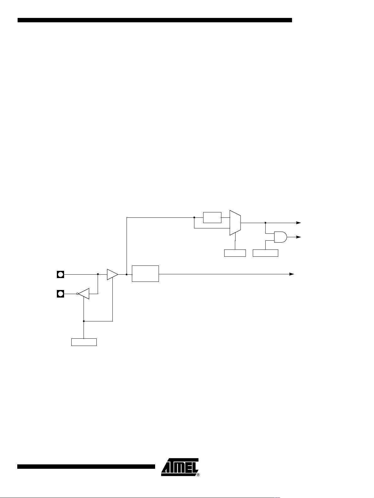
Introduction The AT89C5131 c lock co ntroller is based on an o n-chip oscillat or feedin g an on- chip
Phase Lock Loop (PLL). All the internal clocks to the peripherals and CPU core are generated by this controller.
The AT89C5131 X1 and X2 pins are the input and the output of a single-stage on-chip
inverter (see Figure 5) that can be configured with off-chip components as a Pierce
oscillator (see Figure 6). Value of capacitors and crystal characteristics are detailed in
the section “DC Characteristics”.
The clock controller outputs three different clocks as shown in Figure 5:
• a clock for the CPU core
• a clock for the peripherals which is used to generate the Timers, PCA, WD, and Port
sampling clocks
• a clock for the USB controller
These clocks are enabled or disabled depending on the power reduction mode as
detailed in Section “Power Management”, page 145.
Figure 5. Oscillator Block Diagram
÷ 2
X1
X2
PD
PCON.1
PLL
Oscillator Two clock sources are available for CPU:
• Crystal oscillator on X1 and X2 pins: Up to 32 MHz
In order to optimize the power consumption, the oscillator inverter is inactive when the
PLL output is not selected for the USB device.
0
1
X2
CKCON.0
Peripheral
Clock
CPU Core
Clock
IDL
PCON.0
USB
Clock
4136A–USB–03/03
19
Page 20
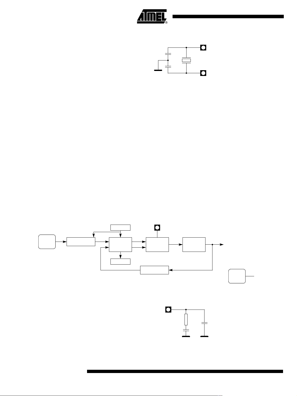
Figure 6. Crystal Connection
X1
C1
Q
C2
VSS
X2
PLL
PLL Description The AT89 C513 1 P LL is us ed to gen er ate int ernal hi gh f re que ncy c lo ck ( the USB Cl ock)
synchronized with an external low-frequency (the Perip heral Clock) . The PLL c lock is
used to generate the USB interface clock. Figure 7 shows the internal structure of the
PLL.
The PFLD block is the Phase Frequency Comparator and Lock Detector. This block
makes the comparison between the reference clock coming from the N divider and the
reverse clock coming from the R divider and generates some pulses on the Up or Down
signal dependin g on the edge posi tion of the r everse c lock. The P LLEN bit in PLLCO N
register is used to enab le the c lock gene ratio n. When the PLL is l ocked, th e bit PL OCK
in PLLCON register (see Figure 7) is set.
The CHP block is the Charge Pump that generates the voltage reference for the VCO by
injecting or extracting charges from the external filter connected on PLLF pin (see
Figure 8). Value of the filter components are detailed in the Section “DC
Characteristics”.
The VCO block is the Voltage Controlled Oscillator controlled by the voltage V
duced by the charge pump. It generates a square wave signal: the PLL clock.
Figure 7. PLL Block Diagram and Symbol
OSC
CLOCK
N divider
N3:0
Figure 8. PLL Filter Connection
PLLCON.1
PLLEN
PFLD
PLOCK
PLLCON.0
USBclk
Up
Down
OSCclk R 1+()×
-----------------------------------------------=
PFILT
CHP
R divider
R3:0
N1+
PFILT
Vref
VCO USB Clock
CLOCK
USB Clock Symbol
R
C1
VSS
C2
VSS
USB
REF
pro-
20
The typical values are: R = 100 Ω, C1 = 10 nf, C2 = 2.2 nF.
AT89C5131
4136A–USB–03/03
Page 21
AT89C5131
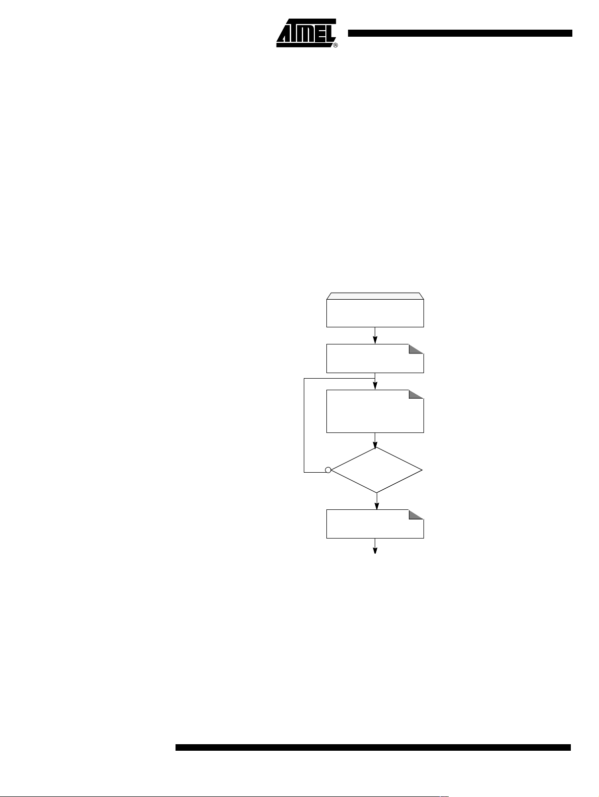
PLL Programming The PLL is progra mmed u sing the flo w sho wn in Figure 9. As s oon as clock gene ratio n
is enabled user must wait until the lock indicator is set to ensure the clock output is
stable.
Figure 9. PLL Programming Flow
PLL
Programming
Configure Dividers
N3:0 = xxxxb
R3:0 = xxxxb
Enable PLL
PLLEN = 1
PLL Locked?
LOCK = 1?
Divider Values To generate a 48 MHz clock using the PLL, the divider values have to be configured fol-
lowing the oscillator frequency. The typical divider values are shown in Table 25.
Table 25. Typical Divider Values
Oscillator Frequency R+1 N+1 PLLDIV
3 MHz 16 1 F0h
6 MHz 8 1 70h
8 MHz 6 1 50h
12 MHz 4 1 30h
16 MHz 3 1 20h
18 MHz 8 3 72h
20 MHz 12 5 B4h
24 MHz 2 1 10h
32 MHz 3 2 21h
40 MHz 12 10 B9h
4136A–USB–03/03
21
Page 22

Registers Table 26. CKCON0 (S:8Fh)
Clock Control Register 0
76543210
- WDX2 PCAX2 SIX2 T2X2 T1X2 T0X2 X2
Bit Number
7-
6WDX2
5PCAX2
4SIX2
3T2X2
2T1X2
Bit
Mnemonic Description
Reserved
The value read from this bit is always 0. Do not set this bit.
Watchdog Clock
This control bit is validated when the CPU clock X2 is set. When X2 is low,
this bit has no effect.
Clear to select 6 clock periods per peripheral clock cycle.
Set to select 12 clock periods per peripheral clock cycle.
Programmable Counter Array Clock
This control bit is validated when the CPU clock X2 is set. When X2 is low,
this bit has no effect.
Clear to select 6 clock periods per peripheral clock cycle.
Set to select 12 clock periods per peripheral clock cycle.
Enhanced UART Clock (Mode 0 and 2)
This control bit is validated when the CPU clock X2 is set. When X2 is low,
this bit has no effect.
Clear to select 6 clock periods per peripheral clock cycle.
Set to select 12 clock periods per peripheral clock cycle.
Timer2 Clock
This control bit is validated when the CPU clock X2 is set. When X2 is low,
this bit has no effect.
Clear to select 6 clock periods per peripheral clock cycle.
Set to select 12 clock periods per peripheral clock cycle.
Timer1 Clock
This control bit is validated when the CPU clock X2 is set. When X2 is low,
this bit has no effect.
Clear to select 6 clock periods per peripheral clock cycle.
Set to select 12 clock periods per peripheral clock cycle.
22
AT89C5131
Timer0 Clock
This control bit is validated when the CPU clock X2 is set. When X2 is low,
1T0X2
0X2
this bit has no effect.
Clear to select 6 clock periods per peripheral clock cycle.
Set to select 12 clock periods per peripheral clock cycle.
System Clock Control bit
Clear to select 12 clock periods per machine cycle (STD mode, F
F
OSC
Set to select 6 clock periods per machine cycle (X2 mode, F
Reset Value = 0000 0000b
/2).
= F
CPU
PER =
CPU = FPER = FOSC
4136A–USB–03/03
).
Page 23

AT89C5131
Table 27. CKCON1 (S:AFh)
Clock Control Register 1
76543210
-------SPIX2
Bit Number
7-1 -
0 SPIX2
Bit
Mnemonic Description
Reserved
The value read from this bit is always 0. Do not set this bit.
SPI Clock
This control bit is validated when the CPU clock X2 is set. When X2 is low,
this bit has no effect.
Clear to select 6 clock periods per peripheral clock cycle.
Set to select 12 clock periods per peripheral clock cycle.
Reset Value = 0000 0000b
Table 28. PLLCON (S:A3h)
PLL Control Register
76543210
------PLLENPLOCK
Bit
Bit Number
7-3 -
Mnemonic Description
Reserved
The value read from this bit is always 0. Do not set this bit.
2-
Reserved
The value read from this bit is always 0. Do not set this bit.
PLL Enable Bit
1 PLLEN
0PLOCK
Set to enable the PLL.
Clear to disable the PLL.
PLL Lock Indicator
Set by hardware when PLL is locked.
Clear by hardware when PLL is unlocked.
Reset Value = 0000 0000b
Table 29. PLLDIV (S:A4h)
PLL Divider Register
76543210
R3 R2 R1 R0 N3 N2 N1 N0
Bit
Bit Number
7-4 R3:0 PLL R Divider Bits
3-0 N3:0 PLL N Divider Bits
Mnemonic Description
Reset Value = 0000 0000
4136A–USB–03/03
23
Page 24
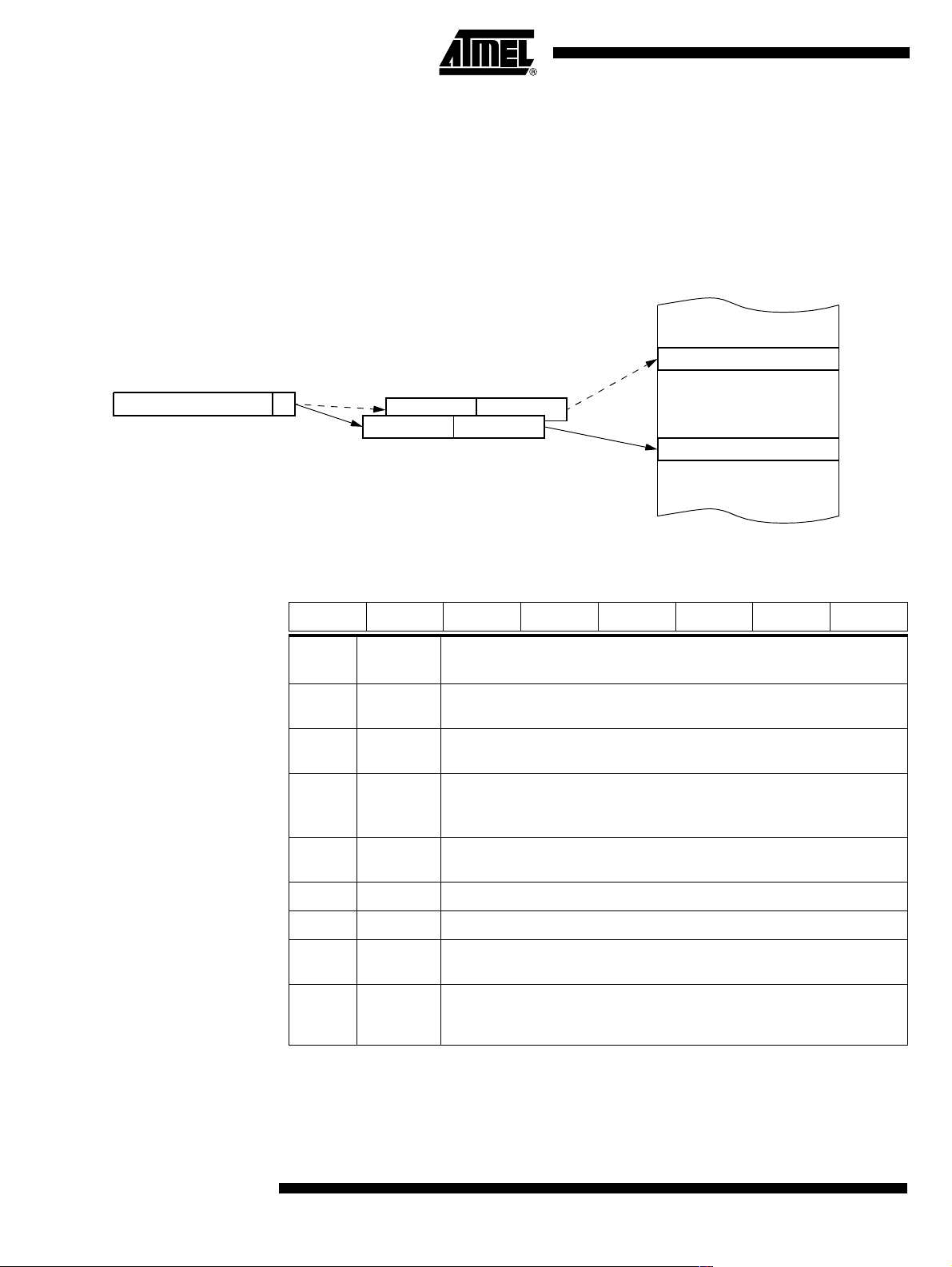
Dual Data Pointer Register
Figure 10. Use of Dual Pointer
AUXR1(A2H)
The additional data pointer can be used to speed up code execution and reduce code
size.
The dual DPTR structure is a way by which the chip will specify the address of an external data memory location. There are two 16-bit DPTR registers that address the external
memory, and a single bit called DPS = AUXR1.0 (see Table 30) that allows the program
code to switch between them (see Figure 10).
External Data Memory
07
DPS
DPTR1
DPTR0
DPH(83H) DPL(82H)
Table 30. AUXR1 Register
AUXR1- Auxiliary Register 1(0A2h)
76543210
- - ENBOOT - GF3 0 - DPS
Bit
Number
7-
6-
5 ENBOOT
4-
3 GF3 This bit is a general-purpose user flag.
2 0 Always cleared.
1-
0DPS
Bit
Mnemonic Description
Reserved
The value read from this bit is indeterminate. Do not set this bit.
Reserved
The value read from this bit is indeterminate. Do not set this bit.
Enable Boot Flash
Cleared to disable boot ROM.
Set to map the boot ROM between F800h - 0FFFFh.
Reserved
The value read from this bit is indeterminate. Do not set this bit.
Reserved
The value read from this bit is indeterminate. Do not set this bit.
Data Pointer Selection
Cleared to select DPTR0.
Set to select DPTR1.
Reset Value = XXXX XX0X0b
Not bit addressable
24
a. Bit 2 stuck at 0; this allows to use INC AUXR1 to toggle DPS without changing GF3.
AT89C5131
4136A–USB–03/03
Page 25

AT89C5131
ASSEMBLY LANGUAGE
; Block move using dual data pointers
; Modifies DPTR0, DPTR1, A and PSW
; note: DPS exits opposite of entry state
; unless an extra INC AUXR1 is added
;
00A2 AUXR1 EQU 0A2H
;
0000 909000MOV DPTR,#SOURCE ; address of SOURCE
0003 05A2 INC AUXR1 ; switch data pointers
0005 90A000 MOV DPTR,#DEST ; address of DEST
0008 LOOP:
0008 05A2 INC AUXR1 ; switch data pointers
000A E0 MOVX A,@DPTR ; get a byte from SOURCE
000B A3 INC DPTR ; increment SOURCE address
000C 05A2 INC AUXR1 ; switch data pointers
000E F0 MOVX @DPTR,A ; write the byte to DEST
000F A3 INC DPTR ; increment DEST address
0010 70F6JNZ LOOP ; check for 0 terminator
0012 05A2 INC AUXR1 ; (optional) restore DPS
INC is a short (2 bytes) and fast (12 clocks) way to manipulate the DPS bit in the AUXR1
SFR. However, note that the INC instruction does not directly force the DPS bit to a particular state, bu t simply togg les it. In simple routines , such as the block mov e examp le,
only the fact that DPS is togg led in th e pr op er se quen ce matt er s, n ot i ts a ctu al val ue. In
other words, th e block m ove rout ine wor ks the sa me wheth er DPS is ’0’ or ’1’ on entry.
Observe that without the last instruction (INC AUXR1), the routine will exit with DPS in
the opposite state.
4136A–USB–03/03
25
Page 26
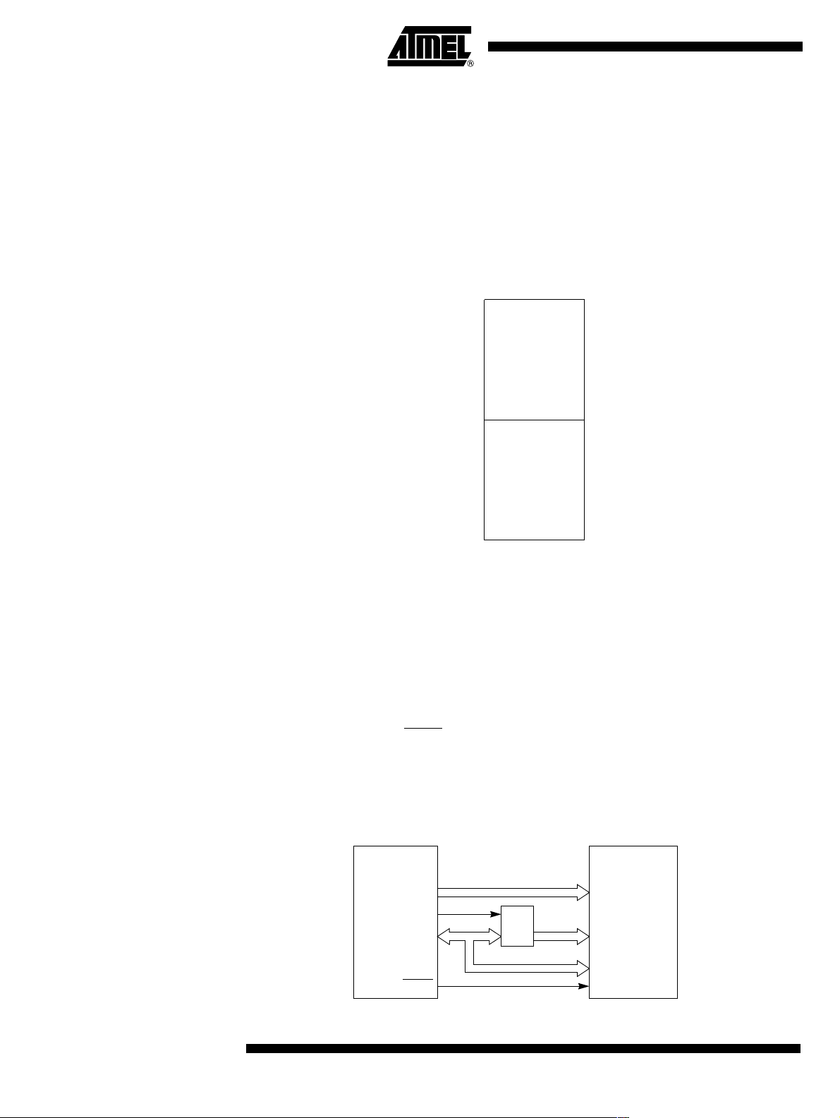
Program/Code Memory
The AT89C5131 implement 32 Kbytes of on-ch ip program/code memory. Figure 11
shows the split of internal and external program/code memory spaces depending on the
product.
The Flash memory increa ses EP ROM and ROM func tional ity by in-cir cui t electric al erasure and programming. Thanks to the internal charge pump, the high voltage needed for
programming or erasing Flash ce lls is gene rated on-chip usi ng the standard V
DD
voltage. Thus, the Flash Memory can be programmed using only one voltage and allows Inapplication Softwa re Progr amming c ommonly known as IAP. Ha rdware programm ing
mode is also available using specific programming tool.
Figure 11. Program/Code Memory Organization
FFFFh
32 Kbytes
External Code
8000h
7FFFh1
32 Kbytes
Flash
0000h
Note: If the program executes exclusively from on-chip code memory (not from external mem-
ory), beware of executing code from the upper byte of on-chip memory (7FFFh) and
thereby disrupting I/O Ports 0 and 2 due to external prefetch. Fetching code constant
from this location does not affect Ports 0 and 2.
AT89C5131
External Code Memory Access
Memory Interfac e The external memory interface comprises the external bus (Port 0 and Port 2) as well as
the bus control signals (PSEN
Figure 12 shows the structure of the external address bus. P0 carries address A7:0
while P2 carries address A15:8. Data D7:0 is multiplexed with A7:0 on P0. Table 31
describes the external memory interface signals.
Figure 12. External Code Memory Interface Structure
AT89C5131
, and ALE).
P2
ALE
P0
AD7:0
A15:8
Latch
A7:0
Flash
EPROM
A15:8
A7:0
26
D7:0
OEPSEN
AT89C5131
4136A–USB–03/03
Page 27
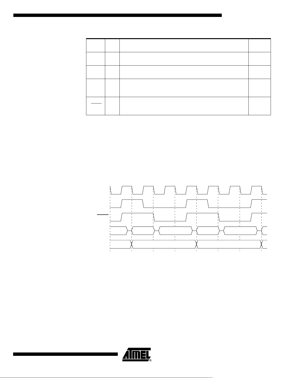
Table 31. External Data Memory Interface Signals
Signal
Name Type Description
AT89C5131
Alternate
Function
A15:8 O
AD7:0 I/O
ALE O
PSEN
Address Lines
Upper address lines for the external bus.
Address/Data Lines
Multiplexed lower address lines and data for the external memory.
Address Latch Enable
ALE signals indicates that valid address information are available on lines
AD7:0.
Program Store Enable Output
O
This signal is active low during external code fetch or external code read
(MOVC instruction).
P2.7:0
P0.7:0
-
-
External Bus Cycles This section describes the bus cycles the AT89C5131 executes to fetch code (see
Figure 13) in the external program/code memory.
External memory cycle takes 6 CPU clock periods. This is equivalent to 12 oscillator
clock periods in standard mode or 6 oscillator clock periods in X2 mode. For further
information on X2 mode (see the clock Section).
For simplicity, the accompanying figure depicts the bus cycle waveforms in idealized
form and do not provide precise timing information.
Figure 13. External Code Fetch Waveforms
CPU Clock
Flash Memory Architecture
ALE
PSEN
P0
P2
D7:0
PCL
PCHPCH
PCLD7:0 D7:0
PCH
AT89C5131 features two on-chip Flash memories:
• Flash memory FM0:
containing 32 Kbytes of program memory (user space) organized into 128-byte
pages,
• Flash memory FM1:
3 Kbytes for bootloader and Application Programming Interfaces (API).
The FM0 supports both paral lel progra mming and Serial In- System Progr ammi ng (IS P)
whereas FM1 supports on ly parallel pr ogramming by progr ammers. The IS P mode is
detailed in the “In-System Programming” section.
All Read/Write access operations on Flash memory by user application are managed by
a set of API described in the “In-System Program mi ng” section.
4136A–USB–03/03
27
Page 28

Figure 14. Flash Memory Architecture
Hardware Security (1 Byte)
Extra Row (128 Bytes)
Column Latches (128 Bytes)
3 Kbytes
Flash Memory
Boot Space
FM1
FFFFh
F400h
7FFFh
32 Kbytes
Flash Memory
User Space
FM0
FM1 mapped between FFFFh and
F400h when bit ENBOOT is set in
AUXR1 re gister
0000h
FM0 Memory Architecture The Flash memory is made up of 4 blocks (see Figure 14):
1. The memory array (user space) 32 Kbytes
2. The Extra Row
3. The Hardware security bits
4. The column latch registers
User Space This space is composed of a 32 Kbytes Flash memory organized in 256 pages of 128
bytes. It contains the user’s application code.
Extra Row (XRow ) This row is a part of FM0 and has a size of 12 8 bytes . The extra r ow may c ontain info r-
mation for bootloader usage.
Hardware Security Space The hardware security space is a part of FM0 and has a size of 1 byte.
The 4 MSB can be read/written by software. Th e 4 LSB can only be read by softwar e
and written by hardware in parallel mode.
Column Latches The column latches, also part of FM0, have a size of full page (128 bytes).
The column latches are the entrance buffers of the three previous memory locations
(user array, XRow and Hardware security byte).
Overview of FM0 Operations
The CPU interfaces to the Flash memor y through the FCON register and AUX R1
register.
These registers are used to:
• Map the memory spaces in the adressable space
• Launch the programming of the memory spaces
• Get the status of the Flash memory (busy/not busy)
• Select the Flash memory FM0/FM1.
Mapping of the Memory Space By default, the user space is accessed by MOVC instruction for read only. The column
latches space is made accessible by setting the FPS bit in FCON register. Writing is
possible from 0000h to 7FFFh, address bits 6 to 0 are used to select an address within a
page while bits 14 to 7 are used to select the programming address of the page.
Setting this bit takes precedence on the EXTRAM bit in AUXR register.
28
AT89C5131
4136A–USB–03/03
Page 29
AT89C5131
The other memory spaces (user, extra row, hardware security) are made accessible in
the code segment by programming bits FMOD0 and FMOD1 in FCON register in accordance with Table 32. A MOVC instruction is then used for reading these spaces.
Table 32. FM0 Blocks Select Bits
FMOD1 FMO D0 FM0 Adressable Space
0 0 User (0000h-FFFFh)
0 1 Extra Row(FF80h-FFFFh)
1 0 Hardware Security (0000h)
1 1 reserved
Launching Programming FPL3:0 bits in FCON r egist er are us ed to sec ure th e launch o f prog ramming . A spe cific
sequence must be written in these bits to unlock the write protection and to launch the
programming. This sequence i s 5 followed by A. Table 33 summarizes the memor y
spaces to program according to FMOD1:0 bits.
Table 33. Programming Spaces
Write to FCON
OperationFPL3:0 FPS FMOD1 FMOD0
5 X 0 0 No action
User
Extra Row
Security
Space
Reserved
AX00
5 X 0 1 No action
AX01
5 X 1 0 No action
A X 1 0 Write the fuse bits space
5 X 1 1 No action
A X 1 1 No action
Write the column latches in user
space
Write the column latches in extra row
space
The Flash memory enters a busy state as soon as programming is launched. In this
state, the memory is not avail abl e for fetc hi ng code. T hus to avoid any erra tic exe cu tio n
during programming, the CPU enters Idle mode. Exit is automatically performed at the
end of programming.
Note: Interrupts that may oc cur during programming time must be disabled to avoid any spuri-
ous exit of the idle mode.
Status of the Flash Memory The bit FBUSY in FCON register is used to indicate the status of programming.
FBUSY is set when programming is in progress.
Selecting FM0/FM1 The bit ENBOOT in AUXR1 register i s used to ch oose between FM0 and FM1 mappe d
up to F800h.
29
4136A–USB–03/03
Page 30
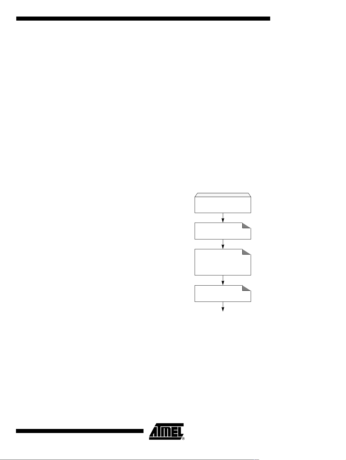
Loading the Column Latches Any nu mbe r of data from 1 byte to 128 bytes c an be load ed in the co lu mn latches . This
provides the capability to program the whole memory by byte, by page or by any number
of bytes in a page.
When progra mmin g is laun ched, a n aut omati c erase of the loc atio ns load ed in th e col umn latches is fi rst per formed, then pr ogrammi ng is eff ectiv ely done . Thus, n o page or
block erase is needed and only the loaded data are programmed in the corresponding
page.
The following procedure is used to load the column latches and is summarized in
Figure 15:
• Map the column latch space by setting FPS bit.
• Load the DPTR with the address to load.
• Load Accumulator register with the data to load.
• Execute the MOVX @DPTR, A instruction.
• If needed loop the three last instructions until the page is completely loaded.
Figure 15. Column Latches Loading Procedure
Column Latches
Loading
Column Latches Mapping
FPS = 1
Data Load
DPTR = Address
ACC = Data
Exec: MOVX @DPTR, A
Last Byte
to load?
Data memory Mapping
FPS = 0
Programming the Flash Spaces
User The following procedure is used to program the User space and is summarized in
Figure 16:
• Load data in the column latches from address 0000h to 7FFFh
(1)
.
• Disable the interrupts.
• Launch the programming by writing the data sequence 50h followed by A0h in
FCON register.
The end of the programming indicated by the FBUSY flag cleared.
• Enable the interrupts.
Note: 1. The last page address used when loading the column latch is the one used to select
the page programming address.
30
AT89C5131
4136A–USB–03/03
Page 31

AT89C5131
Extra Row The following procedure is used to pr ogra m the Extra Row space and i s summ arized i n
Figure 16:
• Load data in the column latches from address FF80h to FFFFh.
• Disable the interrupts.
• Launch the programming by writing the data sequence 52h followed by A2h in
FCON register.
The end of the programming indicated by the FBUSY flag cleared.
• Enable the interrupts.
Figure 16. Flash and Extra Row Programming Procedure
Flash Spaces
Programming
Column Latches Loading
see Figure 15
Disable IT
EA = 0
Launch Programming
FCON = 5xh
FCON = Axh
FBusy
Cleared?
Erase Mode
FCON = 00h
End Programming
Enable IT
EA = 1
4136A–USB–03/03
31
Page 32

Hardware Security The following procedure is used to program the Hardware Security space and is sum-
marized in Figure 17:
• Set FPS and map Hardware byte (FCON = 0x0C)
• Disable the interrupts.
• Load DPTR at address 0000h.
• Load Accumulator register with the data to load.
• Execute the MOVX @DPTR, A instruction.
• Launch the programming by writing the data sequence 54h followed by A4h in
FCON register.
The end of the programming indicated by the FBusy flag cleared.
• Enable the interrupts.
Figure 17. Hardware Programming Procedure
Flash Spaces
Programming
FCON = 0Ch
Data Load
DPTR = 00h
ACC = Data
Exec: MOVX @DPTR, A
Disable IT
EA = 0
Launch Programming
FCON = 54h
FCON = A4h
FBusy
Cleared?
Erase Mode
FCON = 00h
End Programming
Enable IT
EA = 1
32
AT89C5131
4136A–USB–03/03
Page 33
AT89C5131
Reading the Flash Spaces
User The following procedure is used to read the User space and is summarized in Figure 18:
• Map the User space by writing 00h in FCON register.
• Read one byte in Accumulator by executing MOVC A, @A+DPTR with A = 0 &
DPTR = 0000h to FFFFh.
Extra Row The following procedure is used to read the Extra Row space and is summarized in
Figure 18:
• Map the Extra Row space by writing 02h in FCON register.
• Read one byte in Accumulator by executing MOVC A, @A+DPTR with A = 0 &
DPTR = FF80h to FFFFh.
Hardware Security The followi ng procedure is used to read the Hardwar e Security space and is summ a-
rized in Figure 18:
• Map the Hardware Security space by writing 04h in FCON register.
• Read the byte in Accumulator by executing MOVC A, @A+DPTR with A = 0 &
DPTR = 0000h.
Figure 18. Reading Procedure
Flash Spaces Reading
Flash Spaces Mapping
FCON = 00000xx0b
Data Re ad
DPTR = Address
Exec: MOVC A, @A+DPTR
ACC = 0
Erase Mode
FCON = 00h
4136A–USB–03/03
33
Page 34

Registers Table 34. FCON (S:D1h)
Flash Control Register
76543210
FPL3 FPL2 FPL1 FPL0 FPS FMOD1 FMOD0 FBUSY
Bit Number
7-4 FPL3:0
3FPS
2-1 FMOD1:0
0FBUSY
Bit
Mnemonic Description
Programming Launch Command Bits
Write 5Xh followed by AXh to launch the programming according to FMOD1:0.
(see Table 33.)
Flash Map Program Space
Set to map the column latch space in the data memory space.
Clear to re-map the data memory space.
Flash Mode
See Table 32 or Table 33.
Flash Busy
Set by hardware when programming is in progress.
Clear by hardware when programming is done.
Can not be cleared by software.
Reset Value = 0000 0000b
34
AT89C5131
4136A–USB–03/03
Page 35

AT89C5131
Flash EEPROM Memory
General Description The Flash me mory in crease s EPRO M functi onalit y with in -circu it elect rical erasur e and
programming. It contai ns 32 K bytes of program memor y organi zed in 256 pages of 128
bytes, respectively. This memory is both parallel and serial In- System Programmabl e
(ISP). ISP allows devices to alter their own program memory in the actual end product
under software control. A default serial loader (bootloader) pro gram allows ISP of the
Flash.
The programming does not require 12V external programming voltage. The necessary
high programming voltage is generated on-chip using the standard V
microcontroller.
Features • Flash EEPROM internal program memory.
• Boot vector allows user-provided Flash loader code to reside anywhere in the Flash
memory space. This configuration provides flexibility to the user.
• Default loader in Boot EEPROM allows programming via the serial port without the
need of a user provided loader.
• Up to 64K bytes external program memory if the internal program memory is
disabled (EA = 0).
• Programming and erase voltage with standard 5V or 3.3V V
• Read/Program/Erase:
• Byte-wise read (without wait state).
• Byte or page erase and programming (10 ms).
• Typical programming time (32 Kbytes) in 10 sec.
• Parallel programming with 87C51 compatible hardware interface to programmer.
• Programmable security for the code in the Flash.
• 100K write cycles
• 10 years data retention
supply.
CC
pins of the
CC
Flash Programming and Erasure
4136A–USB–03/03
The 32 Kbytes Flash is prog ramme d by bytes or by page s of 128 by tes. It is not ne cessary to erase a byte or a page before programming. The programming of a byte or a
page includes a self erase before programming.
There are three methods of programming the Flash memory:
1. The on-chip ISP bootloader may be invoked which will use low level routines to
program the pages. The interface used for serial downloading of Flash is the
UART.
2. The Flash may be programmed or erased in the end-user application by calling
low-level routines through a common entr y point in the Boot ROM.
3. The Flash may be programmed using the parallel method by using a conven-
tional EPROM programmer. The parallel programming method used by these
devices is similar to that used by EPROM 87C51 but it is not identical and the
commercially available programmers need to have support for the A T89C5131.
The bootloader and the A ppl icati on P r ogram min g Interface (API) routines ar e lo ca ted i n
the Boot ROM.
35
Page 36

Flash Registers and Memory Map
The AT89C5131 Flash memory uses several registers:
• Hardware registers can only be accessed through the parallel programming modes
which are handled by the parallel programme r.
• Software registers are in a special page of the Flash memory which can be
accessed through the API or with the parallel programming modes. This page,
called “Extra Flash Memory”, is not in the internal Flash program memory
addressing space.
Hardware Registers The only hardware registers of the AT89C5131 is called Hardware Security Byte (HSB).
Table 35. Hardware Security Byte (HSB)
76543210
X2 BLJB OSCON1 OSCON0 - LB2 LB1 LB0
Bit
Number
7X2
6BLJB
5-4 OSCON1-0
3-Reserved
2-0 LB2-0
Bit
Mnemonic Description
X2 Mode
Cleared to force X2 mode (6 clocks per instruction)
Set to force X1 mode, Standard Mode (Default).
Bootloader Jump Bit
Set this bit to sta rt th e user’s application on next reset at address 0000h.
Cleared this bit to start the bootloader at address F400h (default).
Oscillator Control Bits
These two bits are used to control the oscillator in order to reduce consummation.
OSCON
1 1 The oscillator is configured to run from 0 to 32 MHz
1 0 The oscillator is configured to run from 0 to 16 MHz
0 1 The oscillator is configured to run from 0 to 8 MHz
0 0 This configuration shouldn’t be set
User Memory Lock Bits
See Table 36
OSCON0 Description
Bootloader Jump Bit (BLJB) One bit of the HSB, the BLJB bit, is used to force the boot address:
• When this bit is set the boot address is 0000h.
• When this bit is reset the boot address is F400h. By default, this bit is cleared and
the ISP is enabled.
Flash Memory Lock Bits The three lock bits provide different levels of protection for the on-chip code and data,
when programmed as shown in Table 36.
36
AT89C5131
4136A–USB–03/03
Page 37

Table 36. Program Lock bits
Program Lock Bit s
1 U U U No program lock features enabled.
2PUU
AT89C5131
Protection DescriptionSecurity level LB0 LB1 LB2
MOVC instruction executed from external
program memory is disabled from fetching code
bytes from any internal memory, EA
and latched on reset, and further parallel
programming of the Flash and of the EEPROM
(boot and Xdata) is disabled. ISP and software
programming with API are still allowed.
is sampled
3XPU
4 X X P Same as 3, also external execution is disabled.
Notes: 1. U: unprogrammed or “one” level.
2. P: programmed or “zero” level.
3. X: don’t care
4. WARNING: Security level 2 and 3 should only be programmed after Flash and code
verification.
Same as 2, also verify through parallel
programming interface is disabled and serial
programming ISP is disabled.
These security bits prote ct the code acces s through the paralle l program ming inte rface.
They are set by default to lev el 4. The code acce ss thr ough the IS P is stil l possib le and
is controlled by the “software security bits” which are stored in the extra Flash memory
accessed by the ISP firmware.
To load a new application with the parallel programmer, a chip erase must be done first.
This will set the HSB in its in activ e stat e and will e rase the Flas h memo ry. The part reference can always be read using Flash parallel programming modes.
Default Values The default value of the HSB provides parts ready to be programmed with ISP:
• BLJB: Cleared to force ISP operation.
• X2: Set to force X1 mode (Standard Mode)
• OSCON1-0: Set to start with 32 MHz oscillator configuration value.
• XRAM: Unprogrammed to valid XRAM
• LB2-0: Security level four to protect the code from a parallel access with maximum
security.
Software Registers Several registers are used, in factory and by parallel programmers, to make copies of
hardware registers con tents . Thes e va lue s are us ed by Atmel ISP (se e Sect ion “In-Sys-
tem Programming (ISP)”).
These registers are in the “Extra Flash Memory” part of the Flash memory. This block is
also called ”XAF” or eXtra Array Flash. They are accessed in the following ways:
• Commands issued by the parallel memory programmer.
• Commands issued by the ISP software.
• Calls of API issued by the application software.
Several software registers are described in Table 37.
37
4136A–USB–03/03
Page 38

Table 37. Software Registers
Mnemonic Description Default value
SBV S oftware Boot Vector FCh –
HSB
BSB Boot Status Byte 0FFh –
SSB S oftware Security Byte FFh –
–
–
–
– Size and Type FBh AT89C5131 16 Kbyte
–
– Revision FFh
Copy of the Hardware
Security Byte
Copy of the Manufacturer
Code
Copy of the Device ID #1:
Family Code
Copy of the Device ID #2:
Memories
Copy of the Device ID #3:
Name
1011 1000b –
58h Atmel
D7h
F7h AT89C5131 32 Kbyte
EFh
C51 X2, Electrically
Erasable
AT89C5131 32 Kbyte,
revision 0
AT89C5131 16 Kbyte,
revision 0
After programming the par t by ISP , the BSB mu st be cl eared (00h) in o rder to al low the
application to boot at 0000h.
The content of the Software Security Byte (SSB) is described in Table 38
and Table 39.
To assure code p rotec ti on f ro m a pa ra ll el ac ce ss , t he H SB mu st al so be at t he r e qui re d
level.
Table 38. Software Security Byte (SSB)
76543210
38
AT89C5131
------LB1LB0
Bit
Number
7-
6-
5-
4-
3-
2-
1-0 LB1-0
Bit
Mnemonic Description
Reserved
Do not clear this bit.
Reserved
Do not clear this bit.
Reserved
Do not clear this bit.
Reserved
Do not clear this bit.
Reserved
Do not clear this bit.
Reserved
Do not clear this bit.
User Memory Lock Bits
See Table 39
4136A–USB–03/03
Page 39

AT89C5131
The two lock bits provide different levels of protection for the on-chip code and data,
when programmed as shown to Table 39.
Table 39. Program Lock Bits of the SSB
Program Lock Bits
Security
Level LB0 LB1
1 U U No program lock features enabled.
2 P U ISP programming of the Flash is disabled.
3 X P Same as 2, also verify through ISP programming interface is disabled.
Notes: 1. U: unprogrammed or "one" level.
2. P: programmed or “zero” level.
3. X: don’t care
4. WARNING: Security level 2 and 3 should only be programmed after Flash and code
verification.
Protection Description
Flash Memory Status AT89C5131 parts are delivered with the ISP boot in the Flash memory. After ISP or par-
allel programming, the possible contents of the Flash memory are summarized in Figure
19:
Figure 19. Flash Memory Possible Contents
7FFFh
AT89C5131
Virgin
Virgin
or
Application
Dedicated
ISP
ApplicationApplication
Virgin
or
Application
Virgin
or
Application
Dedicated
ISP
0000h
Default
After ISP
After ISP
After parallel
programming
After parallel
programming
After parallel
programming
Memory Organization In the AT89C5131, the lowest 16K or 32K of the 64 Kbyte program memory address
space is filled by internal Flash.
When the EA
Bus expansion for accessing program memory from 16K or 32K upward is automatic
since external instruction fetches occur automatically when the program counter
exceeds 3FFFh (16K) or 7FFFh (32K). If the EA
fetches are from external memory. If all storage is on chip, then byte location 3FFFh
(16K) or 7FFFh (32K) should be left vacant to prevent and undesired pre-fetch from
external program memory address 4000h (16K) or 8000h (32K).
4136A–USB–03/03
is pin high, the processor fetches instructions from internal program Flash.
pin is tied low, all program memory
39
Page 40

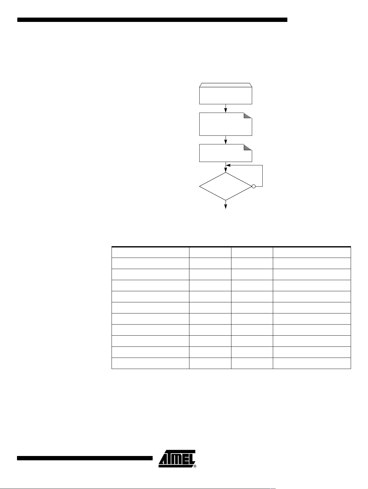
Boot Process
Boot Flash When the user application programs its own Flash memory, all of the low level details
are handled by a code that is permanently contained in a 3 Kbyte “Boot ROM”. A user
program simply calls the common entry point in the Boot ROM with appropriate parameters to accomplis h the desired operation. Bo ot ROM operati ons includ e: erase bloc k,
program byte or page, verify byte or page, program security lock bit, etc. The Boot ROM
is placed in the program memory space at the top of the address space from F800h to
FFFFh (Figure 20).
Figure 20. Boot ROM Loader Memory Map
Boot Process Secondary
FFF0
F400
FFF0
Entry point for API
ISP start
Entry point for API
40
AT89C5131
F400
The boot process is summariz ed in Fi gur e 21.
ISP start
4136A–USB–03/03
Page 41

Figure 21. Boot Process Flowchart
Hardware
AT89C5131
RESET
BLJB = 1?
APPLICATION PROGRAM
Software
No
BSB = = 00h?
0000h address
bit = = 0?
No
Yes
No
No
No
F800h address
P1_CF = FFh?
Yes
P3_CF = FFh?
Yes
P4_CF = FFh?
SBV < 3Fh?
YesYes
Yes
No
4136A–USB–03/03
APPLICATION PROGRAM
ATMEL BOOTLOADER
CUSTOMER BOOTLOADER
PC = [SBV]00h
41
Page 42

In-System Programming (ISP)
The In-System Programmin g (ISP) is performe d without removi ng the microcontroll er
from the system. The ISP facility consists of a series of internal hardware resources
coupled with internal firmware to facilitate remote programming of the AT89C5131
through the serial port.
The Atmel ISP feature has made in-circuit programming in an embedded application
possible with a minimum of additional expenses in components and circuit board area.
Using In-System
Programming
The ISP function through UART uses four pins: TxD, RxD, V
nector needs to be available to in terfac e the applic ation to an external circuit in order to
use this feature.
The ISP feature allows a wide range of baud rates in the user applicati on. It is also
adaptable to a wide rang e of o scilla tor freq uen cies. T his is acco mplis hed by meas urin g
the bit-time of a single bit in a received character. This information is then used to program the baud rate in term s of timer coun ts based on the os cillator frequency . The ISP
feature requires that an initi al cha racter (a n upperc ase U) be s ent to th e AT89C5 131 to
establish the baud rate. The ISP firmware provides auto-echo of received characters.
Once baud rate initialization has been performed, the ISP firmware will only accept Intel
Hex-type records. Intel Hex records consist of ASCII characters used to represent hexadecimal values and are summarized below:
:NNAAAARRDD..DDCC<crlf>
AT89C5131 will accept up to 16 (10h) data bytes. The “AAAA” string represents the
address of the first byte in the record. If there are zero bytes in the record, this field is
often set to ‘‘0000’’. The “RR” string in dicat es the re cord t ype. A rec ord type of “00” is a
data record. A record type of “01” indicates the end-of-file mark. In this application, additional record types will be added to indicate either commands or data for the ISP feature.
The “DD” string represents the data bytes. The maximum number of data bytes in a
record is limited to 16 (decimal). The “CC” string represents the checksum byte. ISP
commands are summarized in Table 40.
As a record is received by the AT89 C5131, the inf ormation in the rec ord is s tored inte rnally and a checksum calculation is performed and compared to ‘‘CC’’.
, VCC. Only a small con-
SS
42
The operation indicated by the record type is not performed until the entire record has
been received. Should an er r or occ ur in th e checksum, the AT89C51 31 wi ll sen d an “X”
out the serial port indicating a checksum error. If the checksum calculation is found to
match the chec ksu m in the recor d, th en th e c omman d wil l be exec uted. In m ost cases ,
successful reception of the record will be indicated by transmitting a “.” character out the
serial port (displaying the contents of the internal program memory is an exception). In
the case of a Data Record (record type ‘‘00’’), an additional check is made. A “.” character will NOT be sent unless the record checksum matched the calculated checksum and
all of the bytes in the record were successfully programmed. For a data record, an “X”
indicates that the checksum failed to match, and an “R” character indicates that one of
the bytes did not properly program.
Atmel_ISP, a software utility to implement ISP programming with a PC, is available from
Atmel. Please visit our web site www.atmel.com.
AT89C5131
4136A–USB–03/03
Page 43

Table 40. Intel-Hex Records Used by In-System Programming
Record Type Command/Data Function
Data Record
:nnaaaa00dd....ddcc
Where:
Nn = number of bytes (hex) in record
00
01
aaaa = memory address of first byte in record
dd....dd = data bytes
cc = checksum
Example:
:05008000AF5F67F060B6
End of File (EOF), no operation
:xxxxxx01cc
Where:
xxxxxx = required field, but value is a “don’t care”
cc = checksum
Example:
:00000001FF
AT89C5131
02
Specify Oscillator Frequency (Not required, left for Philips compatibility)
:01xxxx02ddcc
Where:
xxxx = required field, but value is a “don’t care”
dd = required field, but value is a “don’t care”
cc = checksum
Example:
:0100000210ED
4136A–USB–03/03
43
Page 44

Table 40. Intel-Hex Records Used by In-System Programming (Continued)
Record Type Command/Data Function
Miscellaneous Write Functions
:nnxxxx03ffssddcc
Where:
nn = number of bytes (hex) in record
xxxx = required field, but value is a “don’t care”
03 = Write Function
ff = subfunction code
ss = selection code
dd = data input (as needed)
cc = checksum
Subfunction Code = 01 (Erase Block)
ff = 01
ss = block number in bits 7:5, Bits 4:0 = zeros
Example:
:0200000301A05A erase block 5
Subfunction Code = 04 (Reset Boot Vector and Status Byte)
ff = 04
ss = don’t care
dd = don’t care
Example:
:020000034500F8 Reset boot vector (FCh) and status byte (FFh)
Subfunction Code = 05 (Program Software Security Bits)
03
ff = 05
ss = 00 program software security bit 1 (Level 2 inhibit writing to Flash)
ss = 01 program software security bit 2 (Level 3 inhibit Flash verify)
ss = 02 program security bit 3 (No effect, left for Philips compatibility; disable external
memory is already set in the default hardware security byte)
Example:
:020000030501F6 program security bit 2
Subfunction Code = 06 (Program Boot Status Byte, Boot Vector, X2 bit, Osc bit or BLJB
fuse bit)
ff = 06
ss = 00 program Boot Status byte
ss = 01 program Software Boot vector
ss = 02 program X2 bit
ss = 03 program Osc bit
ss = 04 program BLJB
Example:
:03000003060100F5 program boot vector with 00
Subfunction Code = 07 (Full chip erase)
ff = 07
ss = don’t care
dd = don’t care
Example:
:03000007F5 program boot vector with 00
44
AT89C5131
4136A–USB–03/03
Page 45

AT89C5131
Table 40. Intel-Hex Records Used by In-System Programming (Continued)
Record Type Command/Data Function
Display Device Data or Blank Check
Record type 04 causes the contents of the entire Flash array to be sent out the serial
port in a formatted display. This display consists of an address and the contents of 16
bytes starting with that address. No display of the device contents will occur if security
bit 2 has been programmed. The dumping of the device data to the serial port is
terminated by the reception of any character.
General Format of Function 04
:05xxxx04sssseeeeffcc
Where:
04
05 = number of bytes (hex) in record
xxxx = required field, but value is a “don’t care”
04 = “Display Device Data or Blank Check” function code
ssss = starting address
eeee = ending address
ff = subfunction
00 = display data
01 = blank check
cc = checksum
Example:
:0500000440004FFF0069 (display 4000–4FFF)
In-application Programming Method
Miscellaneous Read Functions
General Format of Function 05
:02xxxx05ffsscc
Where:
02 = number of bytes (hex) in record
xxxx = required field, but value is a “don’t care”
05 = “Miscellaneous Read” function code
ffss = subfunction and selection code
05
0000 = read copy of the signature byte – manufacturer id (58H)
0001 = read copy of the signature byte – device ID# 1 (Family code)
0002 = read copy of the signature byte – device ID # 2 (Memories size and type)
0003 = read copy of the signature byte – device ID # 3 (Product name and revision)
0700 = read the software security bits
0701 = read BSB
0702 = read SBV
0704 = read HSB
cc = checksum
Example:
:020000050001F0 read copy of the signature byte – device id # 1
Several Application Program Interface (API) calls are available for use by an application
program to permit selective erasing and programming of Flash pages. All calls are made
through a common interface, PGM_MTP. The programming fun ctions are selected by
setting up the microcontroller’s registers before making a call to PGM_MTP at FFF0h.
Results are returned in the registers. The API calls are shown in Table 41.
4136A–USB–03/03
A set of Philips compatible API calls is provided.
When several bytes have to be programmed, it is highly recommended to use the Atmel
API “PROGRAM DATA PAGE” call. Indeed, this API call writes up to 128 bytes in a single command.
45
Page 46

Table 41. API Calls
API Call Parameter
PROGRAM DATA BYTE Input Parameters:
R0 = osc freq (integer Not required, left for Philips
compatibility)
R1 = 02h
DPTR = address of byte to program
ACC = byte to program
Return Parameter
ACC = 00 if pass,!00 if fail
PROGRAM DATA PAGE Input Parameters:
R0 = osc freq (integer Not required)
R1 = 09h
DPTR0 = address of the first byte to program in the Flash
memory
DPTR1 = address in XRAM of the first data to program
(second data pointer)
ACC = number of bytes to program
Return Parameter
ACC = 00 if pass,!00 if fail
Remark: number of bytes to program is limited such as
the Flash write remains in a single 128bytes page.
Hence, when ACC is 128, valid values of DPL are 00h,
or, 80h.
ERASE BLOCK Input Parameters:
R0 = osc freq (integer Not required, left for Philips
compatibility)
R1 = 01h
DPH = block number in bits 7:5, bits 4:0 =’0’
DPL = 00h
Return Parameter
None
Remark: Command for Philips compatibility, as no erase
is needed; the ISP firmware write FFh in the
corresponding block.
ERASE BOOT VECTOR Input Parameters:
R0 = osc freq (integer Not required, left for Philips
compatibility)
R1 = 04h
DPH = 00h
DPL = don’t care
Return Parameter
none
46
AT89C5131
4136A–USB–03/03
Page 47

Table 41. API Calls (Continued)
API Call Parameter
PROGRAM SOFTWARE SECURITY BIT Input Parameters:
R0 = osc freq (integer Not required, left for Philips
compatibility)
R1 = 05h
DPH = 00h
DPL = 00h – security bit # 1 (inhibit writing to Flash)
01h – security bit # 2 (inhibit Flash verify)
10h - allows ISP writing to Flash (see Note 1)
11h - allows ISP Flash verify (see Note 1)
Return Parameter
none
PROGRAM BOOT STATUS BYTE Input Parameters:
R0 = osc freq (integer Not required, left for Philips
compatibility)
R1 = 06h
DPH = 00h
DPL = 00h – program status byte
ACC = status byte
Return Parameter
ACC = status byte
AT89C5131
PROGRAM BOOT VECTOR Input Parameters:
R0 = osc freq (integer Not required, left for Philips
compatibility)
R1 = 06h
DPH = 00h
DPL = 01h – program boot vector
ACC = boot vector
Return Parameter
ACC = boot vector
PROGRAM X2 MODE Input Parameters:
R0 = osc freq (integer Not required, left for Philips
compatibility)
R1 = 06h
DPH = 00h
DPL = 02h – program X2 mode at reset
ACC = value (00 or 01h)
Return Parameter
ACC = boot vector
4136A–USB–03/03
47
Page 48

Table 41. API Calls (Continued)
API Call Parameter
PROGRAM OSC MODE Input Parameters:
R0 = osc freq (integer Not required, left for Philips
compatibility)
R1 = 06h
DPH = 00h
DPL = 03h – program OscA/OscB at reset
ACC = value (00 or 01h)
Return Parameter
ACC = boot vector
PROGRAM BLJB Input Parameters:
R0 = osc freq (integer Not required, left for Philips
compatibility)
R1 = 06h
DPH = 00h
DPL = 04h – program FSBt
ACC = value (00 or 01h)
Return Parameter
ACC = boot vector
LOCK MEMORY AREA Input Parameters:
R0 = osc freq (integer Not required, left for Philips
compatibility)
R1 = 0Ch
DPTR0 = address of the first byte to lock in the Flash
memory
DPTR1 =
Return Parameter
none
UNLOCK MEMORY AREA Input Parameters:
R0 = osc freq (integer Not required, left for Philips
compatibility)
R1 = 0Ch
DPTR0 = address of the first byte to lock in the Flash
memory
DPTR1 =
Return Parameter
none
READ DEVICE DATA Input Parameters:
R1 = 03h
DPTR = address of byte to read
Return Parameter
ACC = value of byte read
48
AT89C5131
4136A–USB–03/03
Page 49

Table 41. API Calls (Continued)
API Call Parameter
READ copy of the MANUFACTURER ID Input Parameters:
R0 = osc freq (integer Not required, left for Philips
compatibility)
R1 = 00h
DPH = 00h
DPL = 00h (manufacturer ID)
Return Parameter
ACC = value of byte read
READ copy of the device ID # 1 Input Parameters:
R0 = osc freq (integer Not required, left for Philips
compatibility)
R1 = 00h
DPH = 00h
DPL = 01h (device ID #1)
Return Parameter
ACC = value of byte read
READ copy of the device ID # 2 Input Parameters:
R0 = osc freq (integer Not required, left for Philips
compatibility)
R1 = 00h
DPH = 00h
DPL = 02h (device ID #2)
Return Parameter
ACC = value of byte read
AT89C5131
READ copy of the device ID # 3 Input Parameters:
R0 = osc freq (integer Not required, left for Philips
compatibility)
R1 = 00h
DPH = 00h
DPL = 03h (device ID #2)
Return Parameter
ACC = value of byte read
READ SOFTWARE SECURITY BITS Input Parameters:
R0 = osc freq (integer Not required, left for Philips
compatibility)
R1 = 07h
DPH = 00h
DPL = 00h (Software security bits)
Return Parameter
ACC = value of byte read
READ HARDWARE SECURITY BITS Input Parameters:
R0 = osc freq (integer Not required, left for Philips
compatibility)
R1 = 07h
DPH = 00h
DPL = 04h (Hardware security bits)
Return Parameter
ACC = value of byte read
4136A–USB–03/03
49
Page 50

Table 41. API Calls (Continued)
API Call Parameter
READ BOOT STATUS BYTE Input Parameters:
R0 = osc freq (integer Not required, left for Philips
compatibility)
R1 = 07h
DPH = 00h
DPL = 01h (status byte)
Return Parameter
ACC = value of byte read
READ BOOT VECTOR Input Parame ters:
R0 = osc freq (integer Not required, left for Philips
compatibility)
R1 = 07h
DPH = 00h
DPL = 02h (boot vector)
Return Parameter
ACC = value of byte read
FULL CHIP ERASE Input Parameters:
R0 = osc freq (integer Not required, left for Philips
compatibility)
R1 = 08h
DPH = don’t care
DPL = don’t care
Return Parameter
none
Note: 1. These functions can only be called by user’s code. The standard bootloader cannot
decrease the security level.
50
AT89C5131
4136A–USB–03/03
Page 51

AT89C5131
EEPROM Data Memory
Description The 1-Kbyte on-chip EEPROM memory block is located at addresses 0000h to 03FFh of
the XRAM memory space and is selected by setting control bits in the EECON register.
A read in the EEPROM memory is done with a MOVX instruction.
A physical write i n the E EPRO M memo ry is d one in two step s: write data in the co lumn
latches and transfer of all data latches into an EEPROM memory row (programming).
The number of data written on the page may vary from 1 to 128 bytes (the page size).
When programming, only the data written in the column latch is programmed and a ninth
bit is used to obtain this feature. This provides the capability to program the whole memory by bytes, by page or by a number of b ytes in a page. Indeed, e ach ninth bit is set
when the writing the corr esponding byte in a row and al l these ni nth bits are res et after
the writing of the complete EEPROM row.
Write Dat a i n the Column Latches
Data is written by byte to the column latches as for an external RAM memory. Out of the
11 address bits of t he d ata poi nter, the 4 MSBs are used fo r pag e s ele ct ion ( ro w) and 7
are used for byte selection. Between two EEPROM programming sessions, all the
addresses in the column lat ches mus t stay on the sa me p age, mea ning tha t the 4 MSB
must not be changed.
The following procedure is used to write to the column latches:
• Set bit EEE of EECON register
• Stretch the MOVX to accommodate the slow access time of the column latch (Set
bit M0 of AUXR register)
• Load DPTR with the address to write
• Store A register wit h the data to be written
• Execute a MOVX @DPTR, A
• If needed, loop the three last instructions until the end of a 128 bytes page
Programming The EEPROM programming consists on the following actions:
• Writing one or more bytes of one page in the column latches. Normally, all bytes
must belong to the same page; if not, the first page address will be latched and the
others discarded.
• Launching programming by writing the control sequence (54h followed by A4h) to
the EECON register.
• EEBUSY flag in EECON is then set by hardware to indicate that programming is in
progress and that the EEPROM segment is not available for reading.
• The end of programming is indicated by a hardware clear of the EEBUSY flag.
Read Data The following procedure is used to read the data stored in the EEPROM memory:
• Set bit EEE of EECON register
• Stretch the MOVX to accommodate the slow access time of the column latch (Set
bit M0 of AUXR register)
• Load DPTR with the address to read
• Execute a MOVX A, @DPTR
4136A–USB–03/03
51
Page 52

Registers
Table 42. EECON (S:0D2h)
EECON Register
76543210
EEPL3 EEPL2 EEPL1 EEPL0 - - EEE EEBUSY
Bit Number
7-4 EEPL3-0
3-
2-
1EEE
0EEBUSY
Bit
Mnemonic Description
Programming Launch command bits
Write 5Xh followed by AXh to EEPL to launch the programming.
Reserved
The value read from this bit is indeterminate. Do not set this bit.
Reserved
The value read from this bit is indeterminate. Do not set this bit.
Enable EEPROM Space bit
Set to map the EEPROM space during MOVX instructions (Write in the column
latches)
Clear to map the XRAM space during MOVX.
Programming Busy flag
Set by hardware when programming is in progress.
Cleared by hardware when programming is done.
Cannot be set or cleared by software.
Reset Value = XXXX XX00b
Not bit addressable
52
AT89C5131
4136A–USB–03/03
Page 53

AT89C5131
In-System Programming (ISP)
With the implementation of the User EEPROM and the Boot EEPROM in Flash technology the AT89C5131 allows the system engineer to develop applications with a very high
level of flexibility. This flexibility is based on the possibility to alter the customer programming on all stages of a product’s life:
• During the final production phase, the 1st personalization of the product by parallel
or serial charging of the code in the User EEPROM and if wanted also a customized
Bootloader in the Boot memory (Atmel will provide also a standard Bootloader by
default).
• After assembling of the product in its final stage, embedded position by serial mode
via the USB bus.
This In-System Programming (ISP) allows code modification over the total lifetime of the
product.
Besides the default Boo tloader, Atm el will provide to the c ustome r all the nee ded Application Programmin g Interfac es (AP I) wh ich are needed for ISP. The A PI wi ll be loc ated
in the Boot memory.
This will allow the customer to have a full use of the 32-Kbyte user memory.
Two blocks Flash memories are implemented (see Figure 22):
• Flash memory FM0:
32-Kbytes of program memory organized in a page of 128 bytes,
• Flash memory FM1:
3-Kbytes for default bootloader and Application Programming Interfaces (API).
The FM0 supports both, hardware (parallel) and software progr amming whereas FM1
supports only hardware programming.
The ISP functions are assumed by:
• FCON regis te r and bit ENBO OT in AUX R1 reg ist er
• Bootloader Jump Bit (BLJB), which forces the application execution
• Software Boot Vector (SBV), which can be read and modified by using an API or the
parallel programming mode. The SBV is stored in XROW
• The Extra Byte (EB) and Boot Status Byte (BSB) can be modified only by using API.
EB is stored in XROW
The bit ENBOOT in AUXR1 register allows to map FM 1 between address F400h an d
FFFFh of FM0.
The FM0 can be programmed by:
• The Atmel bootloader, located by default in FM1.
• The user bootloader located in FM0
• The user bootloader located in FM1 in place of Atmel bootloader.
API contained in FM1 can be called b y the user bootloade r located in FM0 at the
address [SBV]00h.
The user program simply calls the common entry point with appropriate parameters in
FM1 to accomplish the desired operation (all these methods will be described in Application Notes on API-description).
4136A–USB–03/03
Boot Flash operations include: erase block, program byte or page, verify byte or page,
program security lock bit, etc. Indeed, Atmel provides the binary code of the default
Flash bootloader.
53
Page 54
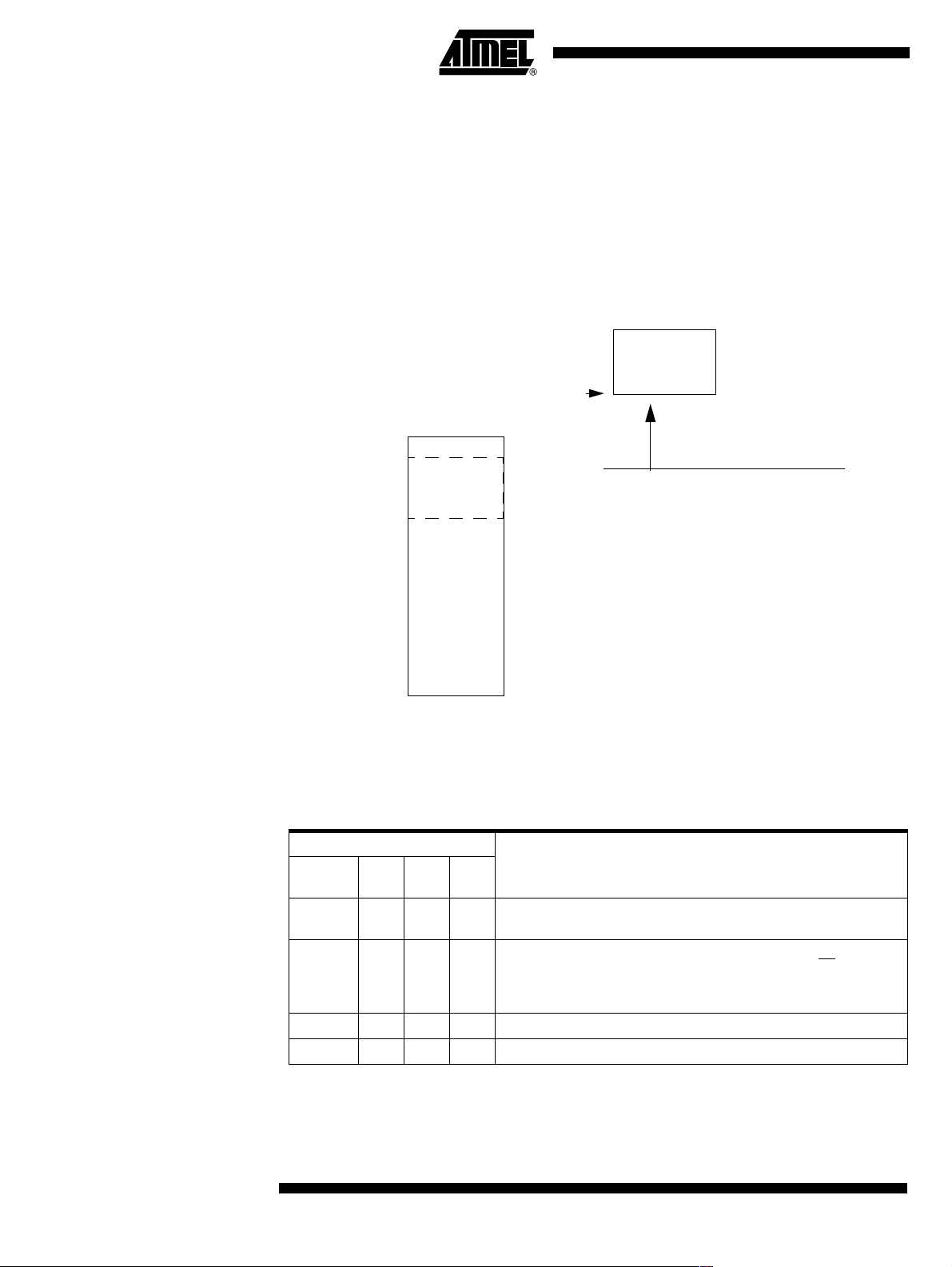
Flash Programming and Erasure
There are three methods of programming the Flash memory:
• The Atmel bootloader located in FM1 is activated by the application. Low level API
routines (located in FM1) to program FM0 will be used. The interface used for serial
downloading to FM0 is the UART or the USB. API can be called also by user’s
bootloader located in FM0 at [SBV]00h.
• A further method exist for activating the Atmel bootloader by using hardware
activation.
• The FM0 can be also programmed by the parallel mode using a programmer.
Figure 22. Flash Memory Mapping
FFFFh
3 Kbytes IAP
Bootloader
F400h
FM1
7FFFh
Custom
Bootloader
[SBV]00h
32 Kbytes
Flash Memory
FM0
FM1 mapped between FFFF and F400
when API called
0000h
Flash Parallel Programming The three lock bits in Hardware byte are programmed according to Table 43. They will
provide different leve l of p rotection fo r the on-c hip code and data l ocated in F M0 and
FM1.
The only way to write these bits are in parallel mode.
Table 43. Program Lock bit
Program Lock Bits
Security
level
1 UUU
2PUU
3 U P U Same as 2, also verify that parallel programming interface is disabled.
4 U U P Same as 3, also external execution is disabled.
LB0 LB1 LB2
Protection Description
No program lock features enabled. MOVC instruction executed from
external program memory returns non encrypted data.
MOVC instruction executed from external program memory are
disabled from fetching code bytes from internal memory, EA
and latched on reset, and further parallel programming of the Flash is
disabled.
is sampled
54
Program Lock bits
U: unprogrammed
P: programmed
AT89C5131
4136A–USB–03/03
Page 55

AT89C5131
WARNING: Security level 2 and 3 should only be programmed after Flash and Core
verification.
Program Lock Bits These security bits protect the co de access through the parallel pr ogrammi ng interf ace.
They are set by default to level 4.
Low Pin-count Boot Process
The bootloader can be activated by two mean s: Regular boot process or Hardwar e
condition.
The hardware condition must be configured by the user using the P1_CF, P3_CF and
P4_CF bytes.
The hardware condition is detected by a low level on the corresponding input.
Example: Configure the pin 2 of the port 3 as Hardware condition.
The corresponding value for these bytes are:
P1_CF = FFh
P3_CF = FBh
P4_CF = FFh
Note: If more than 1 nit of P1_CF, P3_CF and P4_CF are to zero, the higher priority is on
P1_CF.0, the lowest priority is on P4_CF.1
The bootloader USB must be activated if the BLJB = 0.
The on-chip bootloader boot process is shown Figure 23.
Purpose
The Bootloader Jump Bit forces the application execution.
BLJB = 0 = > Bootloader execution.
BLJB = 1 = > Application execution
BLJB
The BLJB is a fuse bit in the Hardware Byte.
That can be modified by hardware (programmer) or by software (API).
Note: 1. The BLJB test is perform by hardware to prevent any program
execution.
4136A–USB–03/03
The Software Boot Vector contains the high address of customer bootloader
SBV
P1_CF
P3_CF
P4_CF
stored in the application.
SBV = FCh (default value) if no customer bootloader in user Flash.
Note: The customer bootloader is called by JMP [SBV]00h instruction.
The P1_CF can contain the user condition for Hardware condition on Port 1
P1_CF is a byte of the XROW area
The P3_CF can contain the user condition for Hardware condition on Port 3
P3_CF is a byte of the XROW area
The P4_CF can contain the user condition for Hardware condition on Port 4
P4_CF is a byte of the XROW area
All routines for software access ar e provided in the C Flash dri ver (see reference
section).
Example of boot process in FM1 (see Figure 23)
55
Page 56
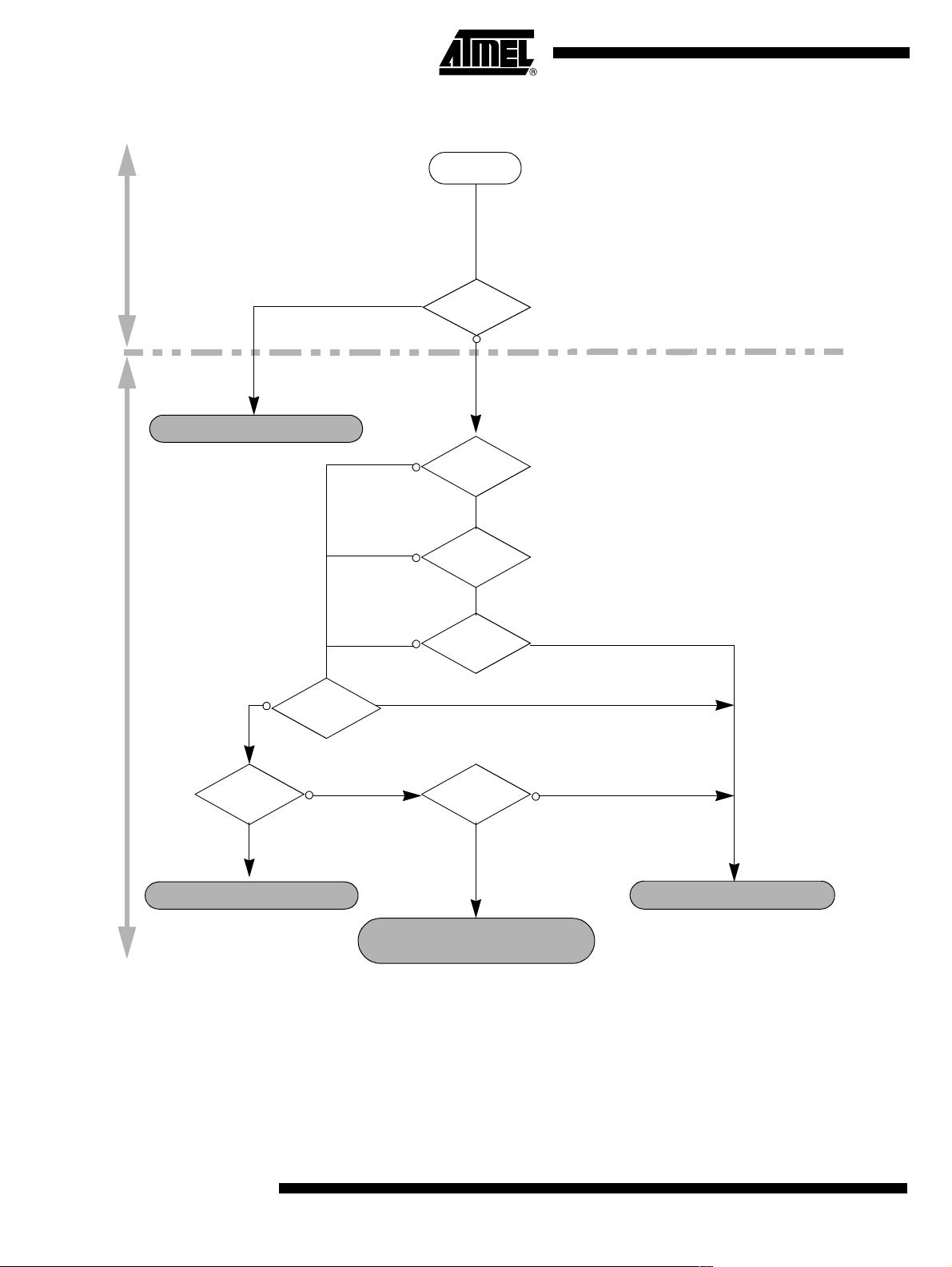
Figure 23. Low Pin-count Boot Process Algorithm
Hardware
RESET
BLJB = 1?
APPLICATION PROGRAM
Software
No
BSB = = 00h?
0000h address
bit = = 0?
No
Yes
No
No
No
F400h address
P1_CF = FFh?
Yes
P3_CF = FFh?
Yes
P4_CF = FFh?
SBV < 3Fh?
YesYes
Yes
No
APPLICATION PROGRAM
High Pin-Count Boot Process
56
AT89C5131
ATMEL BOOTLOADER
CUSTOMER BOOTLOADER
PC = [SBV]00h
At the falling edge of RESET, the bit ENBOOT in AUXR1 register is initialized with the
value of Bootloader Jump Bit (BLJB).
Further at the fa lling edge of RE SET i f the follow ing c ondition s ( called Hardwa re cond ition) are detected:
• PSEN low
• EA high
4136A–USB–03/03
Page 57

• ALE high (or not connec ted )
– After Hardware Condition the FCON register is initialized with the value 00h
and the PC is initialized with F800h (FM1).
The Hardware condition makes the bootloader to be executed, whatever BLJB value is.
If no hardware condition is detected, the FCON register is initialized with the value F0h.
Check of the BLJB value.
• If bit BLJB = 1:
User application in FM0 will be started at 0000h (standard reset).
• If bit BLJB = 0:
Bootloader will be started at F800h in FM1.
Figure 24. Hardware Boot Process Algorithm
AT89C5131
RESET
Hardware
Condition?
Hardware
ENBOOT = 0
PC = 0000h
No
No
BLJB = = 0
Yes
FCON = F0h
?
ENBOOT = 1
PC = F400h
bit ENBOOT in AUXR1 register
is initialized with BLJB.
ENBOOT = 1
PC = F400h
FCON = 00h
Yes
4136A–USB–03/03
Software
Application
in FM0
Bootloader
in FM1
57
Page 58

Application Programming Interface
Several Application Program Interface (API) calls are available for use by an application
program to permit selective erasing and programming of Flash pages. All calls are made
by functions.
All these APIs will be described in an application note.
API Call Description
PROGRAM DATA BYTE Write a byte in Flash memory
PROGRAM DATA PAGE Write a page (128 bytes) in Flash memory
PROGRAM EEPROM BYTE Write a byte in EEPROM memory
ERASE BLOCK Erase all Flash me mory
ERASE SW BOOT VECTOR (SBV) Erase the software boot vector
PROGRAM SW BOOT VECTOR (SBV) Write the software boot vector
ERASE HW BOOT VECTOR (HBV) Erase the hardware boot vector
PROGRAM HW BOOT VECTOR (HBV) Write the hardware boot vector
PROGRAM EXTRA BYTE (EB) Write the extra byte
READ DATA BYTE
READ EEPROM BYTE
READ FAMILY CODE
READ MANUFACTURER CODE
READ PRODUCT NAME
READ REVISION NUMBER
READ STATUS BIT (BSB) Read the status bit
READ BOOT VECTOR (SBV) Read the boot vector
READ EXTRA BYTE (EB) Read the extra byte
PROGRAM X2 Write the hardware flag for X2 mode
READ X2 Read the hardware flag for X2 mode
PROGRAM BLJB Write the hardware flag BLJB
READ BLJB Read the hardware flag BLJB
Application Remarks • A user bootloader can be mapped at address [SBV]00h. The byte SBV contains the
high byte of the boot address, and can be read and written by API.
• The API can be called during user application, without disabling interrupt.
The interrupts are disabled by some APIs, for complex operations.
58
AT89C5131
4136A–USB–03/03
Page 59

XROW Bytes Table 44. XRow Mapping
Mnemonic Description Default Value Address
BSB Boot Status Byte 00h
SBV Software Boot Vector F4h 01h
P1_CF FFh 02h
P3_CF FFh 03h
P4_CF FFh 04h
SSB Software Security Byte FFh 05h
EB Extra Byte FFh 06h
reserved 07h-2Fh
Manufacturer Code 58h 30h
ID1 Device ID#1: Family code D7h 31h
reserved 32h-5Fh
ID2 Device ID#2: Memories size and type F7h 60h
AT89C5131
ID3 Device ID#3: Name and Revision DFh 61h
reserved 62h-7Fh
Table 45. SBV Register
Software B oot Vector
76543210
ADD 7 ADD 6 ADD 5 ADD 4 ADD 3 ADD 2 ADD 1 ADD 0
Bit
Bit Number
7 - 0 ADD7:0 MSB of user bootloader address location
Mnemonic Description
Notes: 1. Default value after erasing chip: FFh
2. Only accessed by the API or in the parallel programming mode.
Table 46. EB Register
EXTRA BYTE
76543210
--------
Bit Number
Bit
Mnemonic Description
4136A–USB–03/03
7 - 0 - User definition
Notes: 1. Default value after erasing chip: FFh
2. Only accessed by the API or in the parallel programming mode.
59
Page 60

Hardware Byte
Table 47. Hardware Byte
76543210
X2B BLJB OSCON1 OSCON0 - LB2 LB1 LB0
Bit Number
7X2B
6BLJB
5-4 OSCON1-0
3-
2-0 LB2:0 Lock Bits
Bit
Mnemonic Description
X2 Bit
Set this bit to start in standard mode
Clear this bit to start in X2 mode.
Bootloader Jump Bit
Set this bit to start the user’s application on next reset at address 0000h.
Cleared this bit to start the bootloader at address F400h (default).
Oscillator Control Bits
These two bits are used to control the oscillator in order to reduce
consumption.
OSCON1
1 1 oscillator is configured to run from 0 to 32 MHz
1 0 oscillator is configured to run from 0 to 16 MHz
0 1 oscillator is configured to run from 0 to 8 MHz
0 0 this configuration shouldn’t be set
Reserved
The value read from this bit is indeterminate.
OSCON0 Description
Default value after erasing chip: FFh
Notes: 1. Only the 4 MSB bits can be access by software.
2. The 4 LSB bits can only be access by parallel mode.
60
AT89C5131
4136A–USB–03/03
Page 61
AT89C5131
On-chip Expanded RAM (XRAM)
The AT89C5131 provi des addit ional Bytes of random access memor y (RAM) spa ce for
increased data parameter handling and high level language usage.
AT89C5131 devices have expanded RA M in externa l data space; maximum size a nd
location are described in Table 48.
Table 48. Description of Expanded RAM
Address
Part Number XRAM Size
AT89C5131 1024 00h 3FFh
Start End
The AT89C5131 has on-chip data memory that is mapped into the following four separate segments.
1. The Lower 128 bytes of RAM (addresses 00h to 7Fh) are directly and indirectly
addressable.
2. The Upper 128 bytes of RAM (addresses 80h to FFh) are indirectly addressable
only.
3. The Special Function Registers, SFRs, (addresses 80h to FFh) are directly
addressable only.
4. The expanded RAM bytes are indirectly accessed by MOVX instructions, and
with the EXTRAM bit cleared in the AUXR register (see Table 48)
The lower 128 bytes can be accessed by either direct or indirect addressing. The Upper
128 bytes can be accessed by indirect ad dressing only. The Upper 128 bytes occupy
the same address s pa ce as th e S F R. Tha t means they have the s ame ad dr ess, but are
physically separate from SFR space.
Figure 25. Internal and External Data Memory Address
0FFh or 3FFh
XRAM
00
0FFh
Upper
128 bytes
Internal
RAM
indirect accesses
80h 80h
7Fh
Lower
128 bytes
Internal
RAM
direct or indirect
00
accesses
0FFh
Special
Function
Register
direct accesses
00FFh up to 03FFh
0FFFFh
External
Data
Memory
0000
4136A–USB–03/03
61
Page 62

When an instruc tion acc esses a n intern al loca tion abo ve addr ess 7Fh , the CPU kn ows
whether the access is to the upper 128 bytes of data RAM or to SFR space by the
addressing mode used in the instruction.
• Instructions that use direct addressing access SFR space. For example: MOV
0A0H, # data, accesses the SFR at location 0A0h (which is P2).
• Instructions that use indirect addressing access the Upper 128 bytes of data RAM.
For example: MOV atR0, # data where R0 contains 0A0h, accesses the data byte at
address 0A0h, rather than P2 (whose address is 0A0h).
• The XRAM bytes can be accessed by indirect addressing, with EXTRAM bit cleared
and MOVX instructions. This part of memory which is physically located on-chip,
logically occupies the first bytes of external data memory. The bits XRS0 and XRS1
are used to hide a part of the available XRAM as explained in Table 48. This can be
useful if external peripherals are mapped at addresses already used by the internal
XRAM.
• With EXTRAM = 0,
combination with any of the registers R0, R1 of the selected bank or DPTR. An
access to XRAM will not affect ports P0, P2, P3.6 (WR) and P3.7 (RD). For
example, with EXTRAM = 0, MOVX atR0, # data where R0 contains 0A0H,
accesses the XRAM at address 0A0H rather than external memory. An access to
external data memory locations higher than the accessible size of the XRAM will be
performed with the MOVX DPTR instructions in the same way as in the standard
80C51, with P0 and P2 as data/address busses, and P3.6 and P3.7 as write and
read timing signals. Accesses to XRAM above 0FFH can only be done by the use of
DPTR.
• With EXTRAM = 1
80C51. MOVX at Ri will provide an eight-bit address multiplexed with data on Port0
and any output port pins can be used to output higher order address bits. This is to
provide the external paging capability. MOVX @DPTR will generate a sixteen-bit
address. Port2 outputs the high-order eight address bits (the contents of DPH) while
Port0 multiplexes the low-order eight address bits (DPL) with data. MOVX at Ri and
MOVX @DPTR will generate either read or write signals on P3.6 (WR
(RD
).
the XRAM is indirectly addressed, using the MOVX instruction in
, MOVX @Ri and MOVX @DPTR will be similar to the standard
) and P3.7
62
The stack point er (SP) may be l ocated any where in the 256 b ytes RAM ( lower and
upper RAM) internal data memory. The stack may not be located in the XRAM.
The M0 bit allows to stretch the XRAM timings; if M0 is set, the read and write pulses
are extended from 6 to 30 clock p eriods. This is useful to access external slow
peripherals.
AT89C5131
4136A–USB–03/03
Page 63

AT89C5131
Table 49. AUXR Register
AUXR - Auxiliar y Register (8Eh)
76543210
DPU - M0 - XRS1 XRS0 EXTRAM AO
Bit
Number
7DPU
6-
5M0
4-
3XRS1XRAM Size
2XRS0
1EXTRAM
Bit
Mnemonic Description
Disable Weak Pull Up
Cleared to enabled weak pull up on standard Ports.
Set to disable weak pull up on standard Ports.
Reserved
The value read from this bit is indeterminate. Do not set this bit
Pulse length
Cleared to stretch MOVX control: the RD
periods (default).
Set to stretc h M O VX c o ntrol: the RD
periods.
Reserved
The value read from this bit is indeterminate. Do not set this bit
XRS1
0 0 256 bytes
0 1 512 bytes
1 0 768 bytes
1 1 1024 bytes (default)
EXTRAM bit
Cleared to access internal XRAM using MOVX at Ri
Set to acces s e xternal memor y.
and the WR pulse length is 6 clock
and the WR pulse length is 30 clock
XRS0 XRAM siz e
at DPTR.
4136A–USB–03/03
ALE Output bit
0AO
Cleared, ALE is emitted at a constant rate of 1/6 the oscillator frequency (or
1/3 if X2 mode is used) (default).
Set, ALE is active only when a MOVX or MOVC instruction is used.
Reset Value = 0X0X 1100b
Not bit addressable
63
Page 64

Timer 2 The Tim er 2 in the AT89C513 1 is th e sta nda rd C5 2 Ti mer 2. It is a 16 -bit tim er /c oun ter :
the count is maintained by two cascaded eight-bit timer registers, TH2 and TL2. It is
controlled by T2CON (Table 50) and T2MOD (Table 51) registers. Timer 2 operation is
similar to Timer 0 and Timer 1. C/T2
(counter ope ration) as the t imer cloc k inpu t. Sett ing TR2 allows TL 2 to be in cremen ted
by the selected input.
Timer 2 has 3 operatin g m odes: captu re, auto rel oad an d Bau d Rate Gene rator. These
modes are selected by the combination of RCLK, TCLK and CP/RL2
Refer to the Atmel 8-bit microcontroller hardware documentation for the description of
Capture and Baud Rate Generator Modes.
Timer 2 includes the following enhancements:
• Auto-reload mode with up or down counter
• Programmable Clock-output
Auto-reload Mode The Auto-reload mode configures Timer 2 as a 16-bit timer or event counter with auto-
matic reload. If DCEN bit in T2MOD is cleared, Timer 2 behaves as in 80C52 (refer to
the Atmel 8-bit microcontroller hardware description). If DCEN bit is set, Timer 2 acts as
an Up/down timer/counter as shown in Figure 26. In this mode the T2EX pin controls the
direction of count.
When T2EX is high, Timer 2 counts up. Timer overflow occurs at FFFFh which sets the
TF2 flag and gene rates an inter rupt requ est. The overfl ow a lso cause s th e 16 -bit v alu e
in RCAP2H and RCAP2L registers to be loaded into the timer registers TH2 and TL2.
selects F
/12 (timer operation) or external pin T2
OSC
(T2CON).
When T2EX is low, Timer 2 counts down. Timer underflow occurs when the count in the
timer registers TH2 and TL2 equals the value stored in RCAP2H and RCAP2L registers.
The underflow sets TF2 flag and reloads FFFFh into the timer registers.
The EXF2 bit toggles when Timer 2 overflows or underflows according to the direction of
the count. EXF2 does not generate an y interrupt. T his bit can be used to provi de 17-bit
resolution.
64
AT89C5131
4136A–USB–03/03
Page 65

Figure 26. Auto-reload Mode Up/Down Counter (DCEN = 1)
F
CLK PERIPH
: 6
T2
0
1
C/T2
T2CON
AT89C5131
TR2
T2CON
Programmable Clock Output
(DOWN COUNTING RELOAD VALUE)
FFh
(8-bit)
TL2
(8-bit)
RCAP2L
(8-bit)
(UP COUNTING RELOAD VALUE)
FFh
(8-bit)
TH2
(8-bit)
RCAP2H
(8-bit)
T2EX:
if DCEN = 1, 1 = UP
if DCEN = 1, 0 = DOWN
if DCEN = 0, up counting
TOGGLE
TF2
T2CON
T2CON
EXF2
Timer 2
INTERRUPT
In the Clock-out mode, Timer 2 operates as a 50%-duty-cycle, programmable clock generator (See Figu re 27). The inpu t clock i ncremen ts TL2 at fr equenc y F
CLK PERIPH
/2. The
timer repeatedl y counts to o verflow from a l oaded val ue. At overfl ow, the cont ents of
RCAP2H and RCAP2L registers are loaded into TH2 and TL2. In this mode, Timer 2
overflows do not generate inter rupts. The following fo rmula gives the Cl ock-out frequency as a function of the system oscillator frequency and the v alue in the RCAP2H
and RCAP2L registers
4136A–USB–03/03
F
Clock OutFrequency–
--------------------------------------------------------------------------------------------
=
4 65536 RC AP2H– RCAP2L⁄()×
CLKPERIPH
For a 16 MHz system clock, Timer 2 has a programmable frequency range of 61 Hz
(F
CLK PERIPH
16)
/2
to 4 MHz (F
CLK PERIPH
/4). The generated clock signal is brought out to
T2 pin (P1.0).
Timer 2 is programmed for the Clock-out mode as follows:
• Set T2OE bit in T2MOD register.
• Clear C/T2
bit in T2CON register.
• Determine the 16-bit reload value from the formula and enter it in RCAP2H/RCAP2L
registers.
• Enter a 16-bit initial value in timer registers TH2/TL2. It can be the same as the
reload value or a different one depending on the application.
• To start the timer, set TR2 run control bit in T2CON register.
65
Page 66
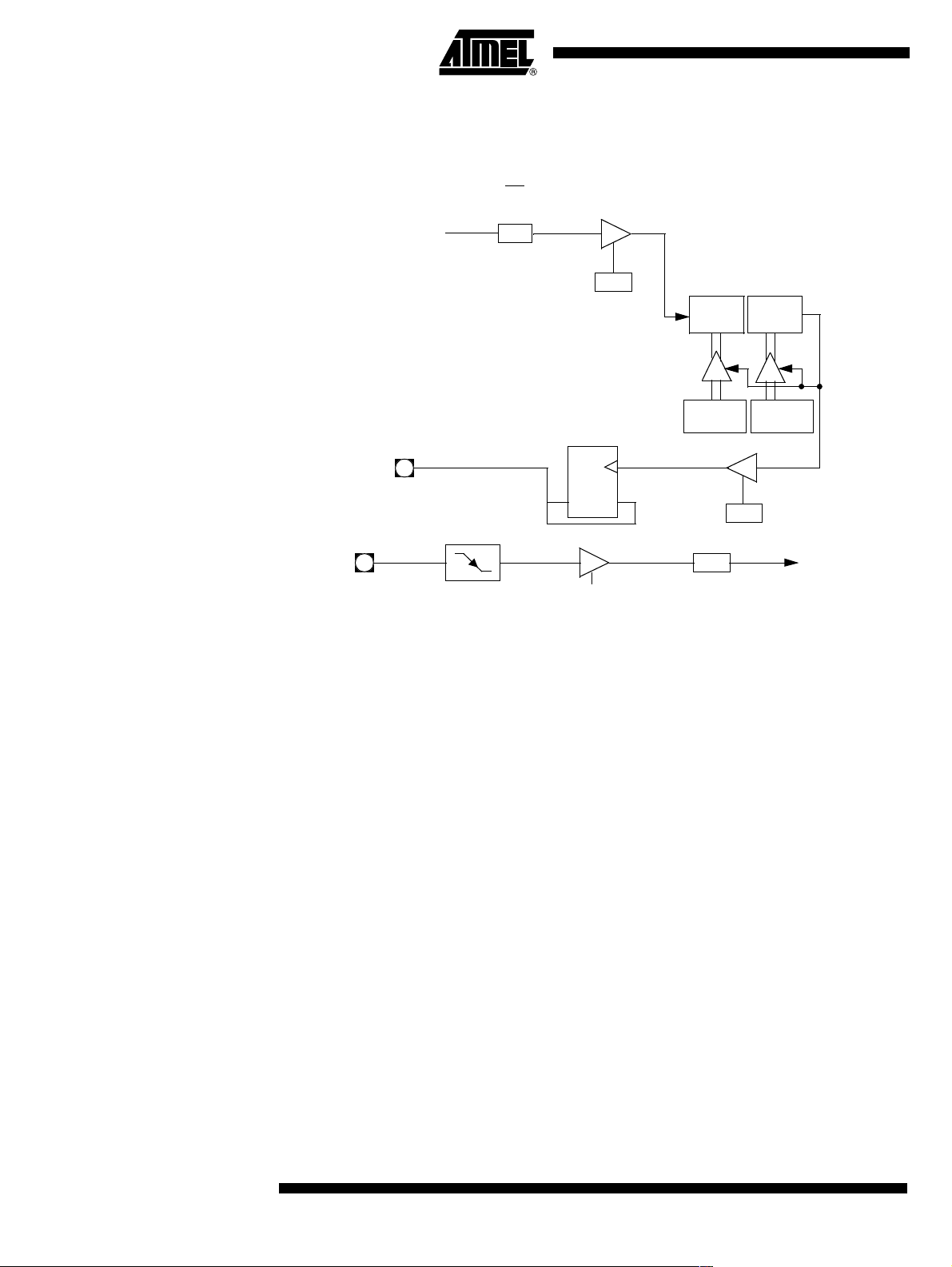
It is possible to use Timer 2 as a baud rate generator and a clock generator simultaneously. For this configuration, the baud rates and clock frequencies are not
independent since both functions use the values in the RCAP2H and RCAP2L registers.
Figure 27. Clock-out Mode C/T2
: 6
T2EX
F
CLK PERIPH
T2
= 0
T2CON
Toggle
QD
EXEN2
T2CON
TR2
TL2
(8-bit)
RCAP2L
(8-bit)
T2MOD
EXF2
T2CON
T2OE
TH2
(8-bit)
RCAP2H
(8-bit)
OVERFLOW
Timer 2
INTERRUPT
66
AT89C5131
4136A–USB–03/03
Page 67

AT89C5131
Table 50. T2CON Register
T2CON - Timer 2 Control Register (C8h)
76543210
TF2 EXF2 RCLK TCLK EXEN2 TR2 C/T2# C P/RL2#
Bit
Number
7 TF2
6EXF2
5 RCLK
4TCLK
3 EXEN2
2TR2
Bit
Mnemonic Description
Timer 2 overflow Flag
Must be cleared by software.
Set by hardware on Timer 2 overflow, if RCLK = 0 and TCLK = 0.
Timer 2 External Flag
Set when a capture or a reload is caused by a negative transition on T2EX pin if
EXEN2 = 1.
When set, causes the CPU to vector to Timer 2 interrupt routine when Timer 2
interrupt is enabled.
Must be cleared by software. EXF2 doesn’t cause an interrupt in Up/down
counter mode (DCEN = 1).
Receive Clock bit
Cleared to use Timer 1 overflow as receive clock for serial port in mode 1 or 3.
Set to use Timer 2 overflow as receive clock for serial port in mode 1 or 3.
Transmit Clock bit
Cleared to use Timer 1 overflow as transmit clock for serial port in mode 1 or 3.
Set to use Timer 2 overflow as transmit clock for serial port in mode 1 or 3.
Timer 2 External Enable bit
Cleared to ignore events on T2EX pin for Timer 2 operation.
Set to cause a capture or reload when a negative transition on T2EX pin is
detected, if Timer 2 is not used to clock the serial port.
Timer 2 Run control bit
Cleared to turn off Timer 2.
Set to turn on Timer 2.
4136A–USB–03/03
Timer/Counter 2 select bit
1C/T2#
0 CP/RL2#
Cleared for timer operation (input from internal clock system: F
Set for counter operation (input from T2 input pin, falling edge trigger). Must be
0 for clock out mode.
Timer 2 Capture/Reload bit
If RCLK = 1 or TCLK = 1, CP/RL2# is ignored and timer is forced to Auto-reload
on Timer 2 overflow.
Cleared to Auto-reload on Timer 2 overflows or negative transitions on T2EX
pin if EXEN2 = 1.
Set to capture on negative transitions on T2EX pin if EXEN2 = 1.
Reset Value = 0000 0000b
Bit addressable
CLK PERIPH
).
67
Page 68

Table 51. T2MOD Register
T2MOD - Timer 2 Mode Control Register (C9h)
76543210
------T2OEDCEN
Bit
Number
7-
6-
5-
4-
3-
2-
1T2OE
0DCEN
Bit
Mnemonic Description
Reserved
The value read from this bit is indeterminate. Do not set this bit.
Reserved
The value read from this bit is indeterminate. Do not set this bit.
Reserved
The value read from this bit is indeterminate. Do not set this bit.
Reserved
The value read from this bit is indeterminate. Do not set this bit.
Reserved
The value read from this bit is indeterminate. Do not set this bit.
Reserved
The value read from this bit is indeterminate. Do not set this bit.
Timer 2 Output Enable bit
Cleared to program P1.0/T2 as clock input or I/O port.
Set to program P1.0/T2 as clock output.
Down Counter Enable bit
Cleared to disable Timer 2 as up/down counter.
Set to enable Timer 2 as up/down counter.
Reset Value = XXXX XX00b
Not bit addressable
68
AT89C5131
4136A–USB–03/03
Page 69

AT89C5131
Programmable Counter Array (PCA)
The PCA provides more timing capabilities with less CPU intervention than the standard
timer/counters. Its advantages include reduced software overhead and improved accuracy. The PCA cons ists of a de dicate d timer/ counter which se rves as the time ba se for
an array of five c ompare /capt ure mod ules. It s cloc k input c an be pr ogramm ed to co unt
any one of the following signals:
• Peripheral clock frequency (F
• Peripheral clock frequency (F
CLK PERIPH
CLK PERIPH
) ÷ 6
) ÷ 2
• Timer 0 overflow
• External input on ECI (P1.2)
Each compare/capture modules can be programmed in any one of the following modes:
• rising and /or falling edg e captu re,
• software timer
• high-speed output, or
• pulse width modulator
Module 4 can also be programmed as a watchdog timer (see Section "PCA Watchdog
Timer", page 79).
When the compare/capture modules are programmed in the capture mode, software
timer, or high speed outpu t mode, an in terrupt c an be gene rated whe n the modu le executes its functio n. All five modules pl us the PCA timer over flow share one interr upt
vector.
The PCA timer/counter and compare/capture modules share Port 1 for external I/O.
These pins are listed below. If the port is not used for the PCA, it c an still be used for
standard I/O.
PCA Component External I/O Pin
16-bit Counter P1.2/ECI
16-bit Module 0 P1.3/CEX0
16-bit Module 1 P1.4/CEX1
16-bit Module 2 P1.5/CEX2
16-bit Module 3 P1.6/CEX3
16-bit Module 4 P1.7/CEX4
The PCA timer is a common time base for all five modules ( see Figure 28). The timer
count source is determined from the CPS1 and CPS0 bits in the CMOD register
(Table 52) and can be programmed to run at:
• 1/6 the
• 1/2 the
peripheral clock frequency (F
peripheral clock frequency (F
CLK PERIPH
CLK PERIPH
).
).
• The Timer 0 overflow
• The input on the ECI pin (P1.2)
4136A–USB–03/03
69
Page 70

Figure 28. PCA Timer/Counter
To PCA
modules
F
CLK PERIPH
F
CLK PERIPH
T0 OVF
Idle
P1.2
/6
CMOD
0xD9
CCON
0xD8
overflow
/2
CIDL CPS1 CPS0 ECF
WDTE
CF CR
CCF4 CCF3 CCF2 CCF1 CCF0
CH CL
16 Bit Up/Down Counter
It
Table 52. CMOD Register
CMOD - PCA Counter Mode Register (D9h)
7 6 5 4 3 2 1 0
CIDL WDTE - - - CPS1 CPS0 ECF
Bit
Number
Bit
Mnemonic Description
Counter Idle Control
7CIDL
Cleared to program the PCA Counter to continue functioning during idle Mode.
Set to program PCA to be gated off during idle.
Watchdog Timer Enable
6WDTE
Cleared to disable Watchdog Timer function on PCA Module 4.
Set to enable Watchdog Timer function on PCA Module 4.
5-
4-
3-
Reserved
The value read from this bit is indeterminate. Do not set this bit.
Reserved
The value read from this bit is indeterminate. Do not set this bit.
Reserved
The value read from this bit is indeterminate. Do not set this bit.
2CPS1PCA Count Pulse Select
CPS1
CPS0 Selected PCA input
0 0 Internal clock f
1CPS0
0 1 Internal clock f
1 0 Timer 0 Overflow
1 1 External clock at ECI/P1.2 pin (max rate = f
PCA Enable Counter Overflow Interrupt
0ECF
Cleared to disable CF bit in CCON to inhibit an interrupt.
Set to enable CF bit in CCON to generate an interrupt.
Reset Value = 00XX X000b
Not bit addressable
CLK PERIPH
CLK PERIPH
/6
/2
CLK PERIPH
/ 4)
70
AT89C5131
4136A–USB–03/03
Page 71

AT89C5131
The CMOD register includes three additional bits associated with the PCA (See
Figure 28 and Table 52).
• The CIDL bit allows the PCA to stop during idle mode.
• The WDTE bit enables or disables the watchdog function on module 4.
• The ECF bit when set causes an interrupt and the PCA overflow flag CF (in the
CCON SFR) to be set when the PCA timer overflows.
The CCON register contains the run control bit for the PCA and the flags for the PCA
timer (CF) and each module (see Table 53).
• Bit CR (CCON.6) must be set by software to run the PCA. The PCA is shut off by
clearing this bit.
• Bit CF: The CF bit (CCON.7) is set when the PCA counter overflows and an
interrupt will be generated if the ECF bit in the CMOD register is set. The CF bit can
only be clear ed by software.
• Bits 0 through 4 are the flags for the modules (bit 0 for module 0, bit 1 for module 1,
etc.) and are set by hardware when either a match or a capture occurs. These flags
can only be cleared by software.
Table 53. CCON Register
CCON - PCA Counter Control Register (D8h)
76543210
CF CR – CCF4 CCF3 CCF2 CCF1 CCF0
Bit
Number
7CF
6CR
5 –
4 CCF4
3 CCF3
2 CCF2
1 CCF1
Bit
Mnemonic Description
PCA Counter Overflow flag
Set by hardware when the counter rolls over. CF flags an int errupt if bit ECF in
CMOD is set. CF may be set by either hardware or software but can only be cleared
by software.
PCA Counter Run control bit
Must be cleared by software to turn the PCA counter off.
Set by software to turn the PCA counter on.
Reserved
The value read from this bit is indeterminate. Do not set this bit.
PCA Module 4 interrupt flag
Must be cleared by software.
Set by hardware when a match or capture occurs.
PCA Module 3 interrupt flag
Must be cleared by software.
Set by hardware when a match or capture occurs.
PCA Module 2 interrupt flag
Must be cleared by software.
Set by hardware when a match or capture occurs.
PCA Module 1 Interrupt Flag
Must be cleared by software.
Set by hardware when a match or capture occurs.
4136A–USB–03/03
PCA Module 0 Interrupt Flag
0 CCF0
Must be cleared by software.
Set by hardware when a match or capture occurs.
Reset Value = 000X 0000b
Not bit addressable
71
Page 72
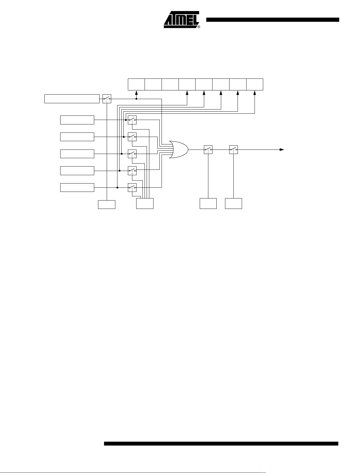
Figure 29. PCA Interrupt System
The watchdog timer function is implemented in module 4 (See Figure 31).
The PCA interrupt system is shown in Figure 29.
PCA Timer/Counter
Module 0
Module 1
Module 2
Module 3
Module 4
CCON
0xD8
To Interrupt
priority decoder
ECF
CF CR
ECCFn
CCF4 CCF3 CCF2 CCF1 CCF0
CCAPMn.0CMOD.0
IE.6 IE.7
EC EA
PCA Modules: each one of t he five compare /capture modules has si x possib le fun ctions. It can perform:
• 16-bit capture, positive-edge triggered
• 16-bit capture, negative-edge triggered
• 16-bit capture, both positive and negative-edge triggered
• 16-bit Software Timer
• 16-bit High-speed Output
• 8-bit Pulse Width Modulator
72
In addition, module 4 can be used as a Watchdog Timer.
Each module in the PCA has a s peci al functi on reg ister ass ocia ted with it. T hese regis-
ters are: CCAPM0 for module 0, CCAPM1 for module 1, etc. (see Table 54). The
registers contain the bits that control the mode that each module will operate in.
• The ECCF bit (CCAPMn.0 where n = 0, 1, 2, 3, or 4 depending on the module)
enables the CCF flag in the CCON SFR to generate an interrupt when a match or
compare occurs in the associated module.
• PWM (CCAPMn.1) enables the pulse width modulation mode.
• The TOG bit (CCAPMn.2) when set causes the CEX output associated with the
module to toggle when there is a match between the PCA counter and the module's
capture/compare register.
• The match bit MAT (CCAPMn.3) when set will cause the CCFn bit in the CCON
register to be set when there is a match between the PCA counter and the module's
capture/compare register.
• The next two bits CAPN (CCAPMn.4) and CAPP (CCAPMn.5) determine the edge
that a capture input will be active on. The CAPN bit enables the negative edge, and
AT89C5131
4136A–USB–03/03
Page 73

AT89C5131
the CAPP bit enables the positive edge. If both bits are set both edges will be
enabled and a capture will occur for either transition.
• The last bit in the register ECOM (CCAPMn.6) when set enables the comparator
function.
Table 55 shows the CCAPMn settings for the various PCA functions.
Table 54. CCAPMn Registers (n = 0-4)
CCAPM0 - PCA Module 0 Compare/Capture Control Register (0DAh)
CCAPM1 - PCA Module 1 Compare/Capture Control Register (0DBh)
CCAPM2 - PCA Module 2 Compare/Capture Control Register (0DCh)
CCAPM3 - PCA Module 3 Compare/Capture Control Register (0DDh)
CCAPM4 - PCA Module 4 Compare/Capture Control Register (0DEh)
7 6 5 4 3 2 1 0
- ECOMn CAPPn CAPNn MATn TOGn PWMn ECCFn
Bit
Number
7-
6ECOMn
5 CAPPn
4CAPNn
3MATn
2TOGn
1PWMn
Bit
Mnemonic Description
Reserved
The value read from this bit is indeterminate. Do not set this bit.
Enable Comparator
Cleared to disable the comparator function.
Set to enable the comparator function.
Capture Positive
Cleared to disable positive edge capture.
Set to enable positive edge capture.
Capture Negative
Cleared to disable negative edge capture.
Set to enable negative edge capture.
Match
When MATn = 1, a match of the PCA counter with this module’s
compare/capture register causes the
CCFn bit in CCON to be set, flagging an interrupt.
Toggle
When TOGn = 1, a match of the PCA counter with this module’s
compare/capture register causes the CEXn pin to toggle.
Pulse Width Modulation Mode
Cleared to disable the CEXn pin to be used as a pulse width modulated output.
Set to enable the CEXn pin to be used as a pulse width modulated output.
4136A–USB–03/03
Enable CCF Interrupt
0CCF0
Cleared to disable compare/capture flag CCFn in the CCON register to
generate an interrupt.
Set to enable compare/capture flag CCFn in the CCON register to generate an
interrupt.
Reset Value = X000 0000b
Not bit addressable
73
Page 74

Table 55. PCA Module Modes (CCAPMn Registers)
ECOMn CAPPn CAPNn M ATn TOGn
0 0 0 0000 No Operation
X 1 0 000X
X 0 1 000X
X 1 1 000X
1 0 0 100X
1 0 0 1 1 0 X 16-bit High Speed Output
1 0 0 00108-bit PWM
10 01X0X
PWMmECCF
n Module Function
16-bit capture by a positiveedge trigger on CEXn
16-bit capture by a negative
trigger on CEXn
16-bit capture by a transition on
CEXn
16-bit Software Timer/Compare
mode.
Watchdog Timer (module 4
only)
There are two additional registers associated with each of the PCA modules. They are
CCAPnH and CCAPnL and these are the registers that store the 16-bit co unt when a
capture occurs or a compare should occur. When a module is used in the PWM mode
these registers are used to control the duty cycle of the output (see Table 56 and
Table 57)
74
AT89C5131
4136A–USB–03/03
Page 75

AT89C5131
Table 56. CCAPnH Registers (n = 0-4)
CCAP0H - PCA Module 0 Compare/Capture Control Register High (0FAh)
CCAP1H - PCA Module 1 Compare/Capture Control Register High (0FBh)
CCAP2H - PCA Module 2 Compare/Capture Control Register High (0FCh)
CCAP3H - PCA Module 3 Compare/Capture Control Register High (0FDh)
CCAP4H - PCA Module 4 Compare/Capture Control Register High (0FEh)
76543210
--------
Bit
Number
7 - 0 -
Bit
Mnemonic Description
PCA Module n Compare/Capture Control
CCAPnH Value
Reset Value = 0000 0000b
Not bit addressable
Table 57. CCAPnL Registers (n = 0-4)
CCAP0L - PCA Module 0 Compare/Capture Control Register Low (0EAh)
CCAP1L - PCA Module 1 Compare/Capture Control Register Low (0EBh)
CCAP2L - PCA Module 2 Compare/Capture Control Register Low (0ECh)
CCAP3L - PCA Module 3 Compare/Capture Control Register Low (0EDh)
CCAP4L - PCA Module 4 Compare/Capture Control Register Low (0EEh)
7 6 5 4 3 2 1 0
- - - - - - - -
Bit
Number
7 - 0 -
Bit
Mnemonic Description
PCA Module n Compare/Capture Control
CCAPnL Value
Reset Value = 0000 0000b
Not bit addressable
4136A–USB–03/03
Table 58. CH Register
CH - PCA Counter Register High (0F9h)
7 6 5 4 3 2 1 0
- - - - - - - -
Bit
Number
7 - 0 -
Bit
Mnemonic Description
PCA counter
CH Value
Reset Value = 0000 0000b
Not bit addressable
75
Page 76

Table 59. CL Register
CL - PCA Counter Register Low (0E9h)
7 6 5 4 3 2 1 0
- - - - - - - -
Bit
Number
7 - 0 -
Bit
Mnemonic Description
PCA Counter
CL Value
Reset Value = 0000 0000b
Not bit addressable
PCA Capture Mode To use one of the PCA modu les in th e captu re mode ei ther one or both of the CCAPM
bits CAPN and CAPP f or tha t mo dul e m us t be s et. Th e ex te rnal CEX i nput for th e m odule (on port 1) is sampled for a transition. When a valid transition occurs the PCA
hardware loads the value of the PCA counter registers (CH and CL) into the module’s
capture registers (CCAPnL and CCAPn H). If the CC Fn bit for the m odule in the CCON
SFR and the ECCFn bit in the CCAPMn SFR are set then an interrupt will be generated
(see Figure 30).
Figure 30. PCA Capture Mode
CF CR
CCF4 CCF3 CCF2 CCF1 CCF0
CCON
0xD8
PCA IT
Cex.n
16-bit Software Timer/Compare Mode
PCA Counter/Timer
CH CL
Capture
CCAPnH CCAPnL
ECOMn
CAPNn MATn TOGn PWMn ECCFnCAPPn
CCAPMn, n = 0 to 4
0xDA to 0xDE
The PCA modules can be used as software timer s by setting both the ECOM and MAT
bits in the modules CCAPMn regi ster. The PCA timer will be compared to the module’s
capture registers and when a match occurs an interrupt will occur if the CCFn (CCON
SFR) and the ECCFn (CCAPMn SFR) bits for the module are both set (see Figure 31).
76
AT89C5131
4136A–USB–03/03
Page 77
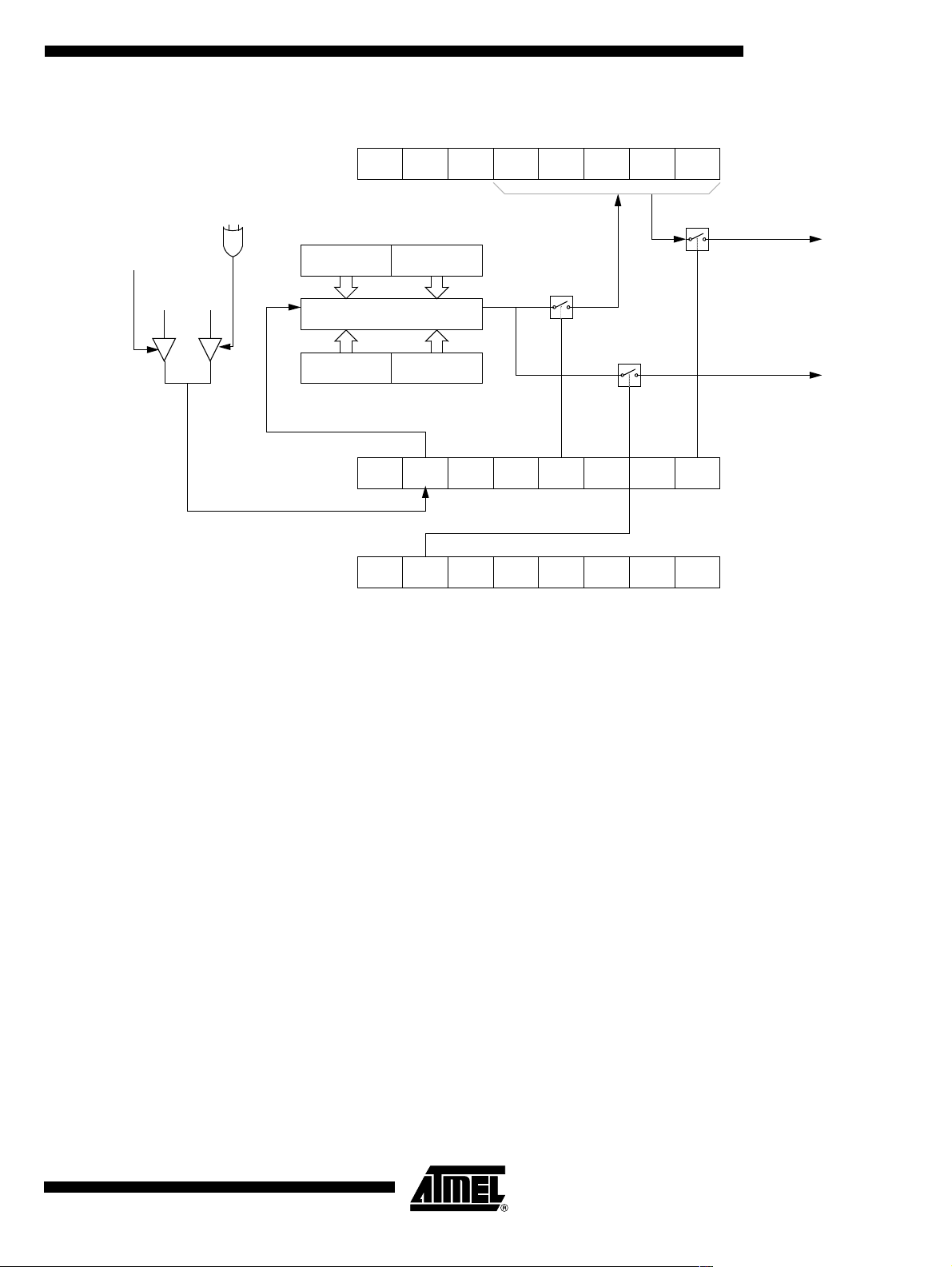
Figure 31. PCA Compare Mode and PCA Watchdog Timer
CF CCF2 CCF1 CCF0
CR
CCF4
CCF3
AT89C5131
CCON
0xD8
Write to
CCAPnH
Write to
CCAPnL
10
Reset
CCAPnH CCAPnL
Enable
16-bit Comparator
CH CL
PCA Counter/Timer
Note: 1. Only for Module 4
Match
ECOMn
CIDL CPS1 CPS0 ECF
WDTE
CAPNn MATn TOGn PWMn ECCFnCAPPn
PCA IT
(1)
RESET
CCAPMn, n = 0 to 4
0xDA to 0xDE
CMOD
0xD9
Before enabling ECO M bi t, CCA P nL a nd CC AP nH s hou ld be s et with a non zero value,
otherwise an unwanted match could happen. Writing to CCAPnH will set the ECOM bit.
Once ECOM set, writing CCAPnL will clear ECOM so that an unwanted match doesn’t
occur while modifying the compare value. Writing to CCA PnH will set ECOM. For this
reason, user software should write CCAPnL first, and then CCAPnH. Of course, the
ECOM bit can still be controlled by accessing to CCAPMn register.
High Speed Output Mode In this mode, the CEX output (on port 1) associated with the PCA module will toggle
each time a match occurs between the PCA counter and the module's capture registers.
To activate this mode the TOG, MAT, and ECOM bits in the module's CCAPMn SFR
must be set (see Figure 32).
A prior write must be done to CCAPnL and CCAPnH before writing the ECOMn bit.
4136A–USB–03/03
77
Page 78
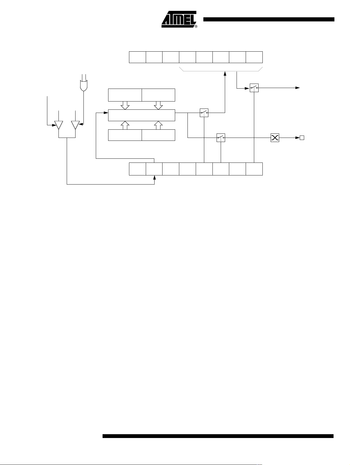
Figure 32. PCA High-speed Output Mode
Write to
CCAPnL
Write to
CCAPnH
Reset
CCAPnH CCAPnL
CF CR
CCF4 CCF3 CCF2 CCF1 CCF0
CCON
0xD8
PCA IT
0
1
Pulse Width Modulator Mode
Enable
16-bit Comparator
CH CL
PCA counter/timer
ECOMn
Match
CAPNn MATn TOGn PWMn ECCFnCAPPn
CEXn
CCAPMn, n = 0 to 4
0xDA to 0xDE
Before enabling ECO M bi t, CCA P nL a nd CC AP nH s hou ld be s et with a non zero value,
otherwise an unwanted match could happen.
Once ECOM set, writing CCAPnL will clear ECOM so that an unwanted match doesn’t
occur while modifying the compare value. Writing to CCA PnH will set ECOM. For this
reason, user software should write CCAPnL first, and then CCAPnH. Of course, the
ECOM bit can still be controlled by accessing to CCAPMn register.
All of the PCA module s can b e used a s PWM out puts. F igure 33 sh ows the PW M function. The frequen cy of t he output depends on the source fo r the P CA time r. All o f the
modules will hav e the sam e freque ncy of outpu t beca use they al l share th e PCA tim er.
The duty cycle of each module is independently variable using the module's capture
register CCAPLn. When the value of the PCA CL SFR is less than the value in the module's CCAPLn SF R th e ou tput w ill be low, w hen it is equal to or g reater than the outpu t
will be high. When CL overflows from FF to 00, CCAP Ln is reloaded with the value i n
CCAPHn. This allows updati ng the PWM wi thout glitch es. The PWM and ECOM bits in
the module's CCAPMn register must be set to enable the PWM mode.
78
AT89C5131
4136A–USB–03/03
Page 79
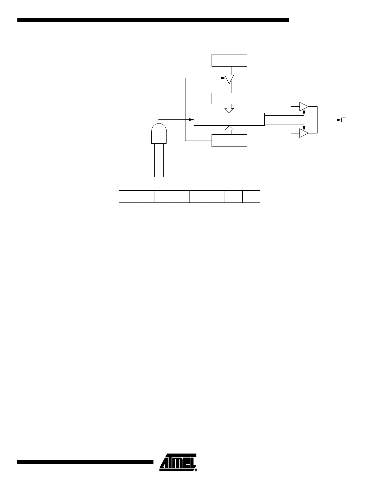
Figure 33. PCA PWM Mode
AT89C5131
CCAPnH
CCAPnL
8-bit Comparator
CL
PCA Counter/Timer
“0”
<
≥
“1”
CCAPMn, n = 0 to 4
0xDA to 0xDE
CEXn
ECOMn
Overflow
Enable
CAPNn MATn TOGn PWMn ECCFnCAPPn
PCA Watchdog Timer An on-board watchdog timer is available with the PCA to imp rove the rel iability of the
system without increasing chip count. Watchdog timers are useful for systems that are
susceptible to noise, power glitches, or electrostatic discharge. Module 4 is the only
PCA module that can be programmed as a watchdog. However, this module can still be
used for other modes i f the watchd og i s n ot ne eded . F igur e 31 shows a di agram of h ow
the watchdog works. The us er pre-loads a 16-bit v alue in the compare reg isters. Jus t
like the other compare modes, this 16-bit value is compared to the PCA timer value. If a
match is allowed to occ ur, an interna l reset will be gener ated. This wi ll not cause the
RST pin to be driven high.
4136A–USB–03/03
In order to hold off the reset, the user has three options:
1. Periodically change the compare value so it will never match the PCA timer
2. Periodically change the PCA timer value so it will never match the compare val-
ues, or
3. Disable the watchdog by clearing the WDTE bit before a match occurs and then
re-enable it
The first two options are more rel iab le becaus e the watc hdog tim er is ne ve r dis abled as
in option #3. If the program coun ter ever goes astray, a mat ch will eve ntually oc cur and
cause an internal res et. T he se co nd o pti on i s als o n ot r ecommended if other PCA m odules are being used. Remember, the PCA timer is the time base for all modules;
changing the time base for other modules would not be a good idea. Thus, in most applications the first solution is the best option.
This watchdog timer won’t generate a reset out on the reset pin.
79
Page 80

Serial I/O Port The serial I/O port in the AT89C5131 is compatible with the serial I/O port in the 80C52.
It provides both synchronous and asynchronous communication modes. It operates as
an Universal Asynchronous Receiver and Transmitt er (UART) in three full-duplex
modes (modes 1, 2 and 3 ). A syn chro nous tr ansm iss ion and r ecep tion ca n occu r si multaneously and at different baud rates.
Serial I/O port includes the following enhancements:
• Framing error detection
• Automatic address recognition
Framing Error Detection Framing bit error detection is provided for the three asynchronous modes (modes 1, 2
and 3). To enable the framin g bi t erro r de tection feature, set SMOD0 bit in PCO N r egi ster (see Figure 34).
Figure 34. Framing Error Block Diagram
RITIRB8TB8RE NSM2SM1SM0/FE
SCON (98h)
Set FE Bit if Stop Bit is 0 (framing error) (SMOD0 = 1
SM0 to UART Mode Control (SMOD0 = 0)
PCON (87h)
IDLPDGF0GF1POF-SMOD0SMOD1
To UART Framing Error Control
When this feature is enabled, the receiver checks each incoming data frame for a valid
stop bit. An invalid stop bit may result from noise on the serial lines or from simultaneous
transmission by two CPUs. If a valid stop bit is not found, the Framing Error bit (FE) in
SCON register (See Table 60) bit is set.
Software may examine FE bit after each reception to check for data errors. Once set,
only software or a reset can clear FE bit. Subsequently received frames with valid stop
bits cannot clear FE b it. W hen FE featur e is enab led, RI rise s on st op bit i nstead of th e
last data bit (See Figure 35 and Figure 36).
Figure 35. UART Timings in Mode 1
RXD
RI
SMOD0 = X
FE
SMOD0 = 1
Start
Bit
Data Byte
D7D6D5D4D3D2D1D0
Stop
Bit
80
AT89C5131
4136A–USB–03/03
Page 81

Figure 36. UART Timings in Modes 2 and 3
RXD
AT89C5131
D8D7D6D5D4D3D2D1D0
Automatic Address Recognition
RI
SMOD0 = 0
RI
SMOD0 = 1
FE
SMOD0 = 1
Start
Bit
Data Byte Ninth
Bit
Stop
Bit
The automatic addr es s rec ogn iti on feat ur e i s en abl ed when the multiprocess or com munication feature is enabled (SM2 bit in SCON register is set).
Implemented i n hardwa re, au tomati c addre ss reco gnition enhan ces the m ultip roces sor
communication feature by allowing the serial port to examine the address of each
incoming command frame. Only when the serial port re cognizes it s own address, the
receiver sets RI bit in SCON register to generate an interrupt. This ensures that the CPU
is not interrupted by command frames addressed to other devices.
If desired, you may enabl e the automatic address re cognition fea ture in mode 1. In this
configuration, the stop bit takes the place of the ninth data bit. Bit RI is set only when the
received command frame address matches the device’s addre ss and is ter min ate d b y a
valid stop bit.
To support automatic a ddr ess re co gni tio n, a dev ic e i s identified by a given add re ss an d
a broadcast address.
Note: The multiprocessor communication and automatic address recognition features cannot
be enabled in mode 0 (i.e., setting SM2 bit in SCON register in mode 0 has no effect).
Given Address Each device has a n ind ivi dual addr ess th at is sp ecif ied i n S ADDR reg iste r; t he SA DEN
register is a mask byte that contains don’t care bits (defined by zeros) to form the
device’s given address. The don’t care bits provide the flexibility to address one or more
slaves at a time. The following example illustrates how a given address is formed.
To address a device by its individual address, the SADEN mask byte must be 1111
1111b.
For example:
SADDR0101 0110b
SADEN
1111 1100b
Given0101 01XXb
The following is an example of how to use given addresses to address different slaves:
Slave A:SADDR1111 0001b
SADEN
1111 1010b
Given1111 0X0Xb
Slave B:SADDR1111 0011b
Slave C:SADDR1111 0010b
1111 1001b
SADEN
Given1111 0XX1b
1111 1101b
SADEN
Given1111 00X1b
4136A–USB–03/03
81
Page 82

The SADEN byte is selected so that each slave may be addressed separately.
For slave A, bit 0 (the LSB) is a don’t care bit; for sl av es B a nd C, bit 0 is a 1. T o comm u-
nicate with slave A only, the master must send an address where bit 0 is clear (e.g.
1111 0000b).
For slave A, bit 1 is a 1; for slaves B and C, bit 1 is a don’t care bit. To communicate with
slaves B and C, but not slave A, the master must send an address with bits 0 and 1 both
set (e.g. 1111 0011b).
To communicate with slaves A, B and C, the master must send an address with bit 0 set,
bit 1 clear, and bit 2 clear (e.g. 1111 0001b).
Broadcast Address A broadcast address is formed from the logical OR of the SADDR and SADEN registers
with zeros defined as don’t care bits, e.g.:
SADDR0101 0110b
S ADEN1111 1100b
Broadcast = SADDR OR SADEN1111 111Xb
The use of don’t care bits provides flexibility in defining the broadcast address, in most
applications, a broadcast address is FFh. The following is an example of using broadcast addresses:
Slave A:SADDR1111 0001b
SADEN
1111 1010b
Broadcast1111 1X11b,
Slave B:SADDR1111 0011b
Slave C:SADDR = 1111 0010b
1111 1001b
SADEN
Broadcast1111 1X11B,
1111 1101b
SADEN
Broadcast1111 1111b
For slaves A and B, bit 2 is a don’t care bit; for slave C, bit 2 is set. To communicate with
all of the slaves, the ma ster must se nd an add ress F Fh. To c ommun icate with sl aves A
and B, but not slave C, the master can send and address FBh.
Reset Addresses On reset, the SADDR and SADEN registers are initialized to 00h, i.e. the given and
broadcast addresses ar e XXXX XXXXb (all don’t car e bits). Thi s ensure s that the seria l
port will reply to any address, and so, that it is backwar ds compatible with the 80C5 1
microcontrollers that do not support automatic address recognition.
SADEN - Slave Address Mask Register (B9h)
7 6 5 4 3 2 1 0
Reset Value = 0000 0000b
Not bit addressable
82
AT89C5131
4136A–USB–03/03
Page 83
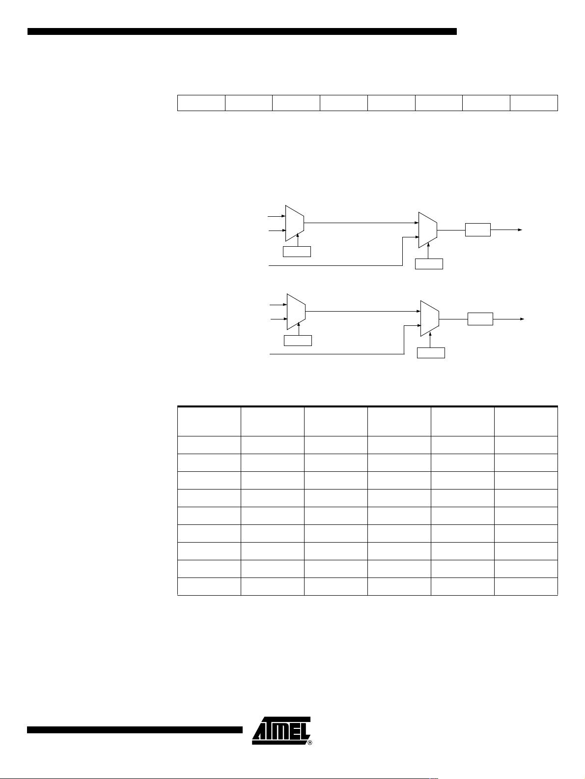
AT89C5131
SADDR - Slave Address Register (A9h)
7 6 5 4 3 2 1 0
Reset Value = 0000 0000b
Not bit addressable
Baud Rate Selection for UART for Mode 1 and 3
Baud Rate Selection Table for
UART
The Baud Rate Generator for transmit and receive clocks can be selected separately via
the T2CON and BDRCON registers.
Figure 37. Baud Rate Selection
TIMER1
TIMER2
INT_BRG
TIMER1
TIMER2
INT_BRG
TCLK
(T2CON)
0000Timer 1Timer 1
(T2CON)
0
1
RCLK
0
1
TCLK
RCLK
TIMER_BRG_RX
TIMER_BRG_TX
TBCK
(BDRCON)
RBCK
(BDRCON)
0
1
RBCK
0
1
TBCK
Clock Source
/ 16
UART Tx
/ 16
Rx Clock
Tx Clock
Clock Source
UART Rx
Internal Baud Rate Generator
(BRG)
4136A–USB–03/03
1000Timer 2Timer 1
0100Timer 1Timer 2
1100Timer 2Timer 2
X 0 1 0 INT_BRG Timer 1
X 1 1 0 INT_BRG Timer 2
0 X 0 1 Timer 1 INT_BRG
1 X 0 1 Timer 2 INT_BRG
X X 1 1 INT_BRG INT_BRG
When the internal B au d Ra te Generator is used, t he Bau d Ra tes a re de ter mi ned by th e
BRG overflow depending on the BRL reload value, the value of SPD bit (Speed Mode)
in BDRCON register and the value of the SMOD1 bit in PCON register.
83
Page 84

Figure 38. Internal Baud Rate
CLK PERIPH
BRR
auto reload counter
/6
0
1
SPD
BRG
BRL
overflow
• The baud rate for UART is token by formula:
SMOD1
Baud_Rate =
(BRL) = 256 -
2
2 x 2 x 6
2
2 x 2 x 6
x FCLK PERIPH
(1-SPD)
x 16 x [256 - (BRL)]
SMOD1
x FCLK PERIPH
(1-SPD)
x 16 x Baud_Rate
/2
0
INT_BRG
1
SMOD1
84
AT89C5131
4136A–USB–03/03
Page 85

AT89C5131
Table 60. SCON Register – SCON Serial Control Register (98h)
76543210
FE/SM0 SM1 SM2 REN TB8 RB8 TI RI
Bit
Number
7
6SM1
5SM2
4REN
3TB8
Bit
Mnemonic Description
FE
SM0
Framing Error bit (SMOD0 = 1)
Clear to reset the error state, not cleared by a valid stop bit.
Set by hardware when an invalid stop bit is detected.
SMOD0 must be set to enable access to the FE bit
Serial port Mode bit 0
Refer to SM1 for serial port mode selection.
SMOD0 must be cleared to enable access to the SM0 bit
Serial port Mode bit 1
SM1 Mode Description Baud Rate
SM0
0 0 0 Shift Register F
0 1 1 8-bit UART Variable
1 0 2 9-bit UART F
1 1 3 9-bit UART Variable
Serial port Mode 2 bit/Multiprocessor Communication Enable bit
Clear to disable multiprocessor communication feature.
Set to enable multiprocessor communication feature in mode 2 and 3, and
eventually mode 1. This bit should be cleared in mode 0.
Reception Enable bit
Clear to disable serial reception.
Set to enable serial reception.
Transmitter Bit 8/Ninth bit to Transmit in Modes 2 and 3
Clear to transmit a logic 0 in the 9th bit.
Set to transmit a logic 1 in the 9th bit.
CPU PERIPH
CPU PERIPH/
/6
32 or/16
Receiver Bit 8/Ninth bit received in modes 2 and 3
2RB8
1TI
0RI
Cleared by hardware if 9th bit received is a logic 0.
Set by hardware if 9th bit received is a logic 1.
In mode 1, if SM2 = 0, RB8 is the received stop bit. In mode 0 RB8 is not used.
Transmit Interrupt flag
Clear to acknowledge interrupt.
Set by hardware at the end of the 8th bit time in mode 0 or at the beginning of the
stop bit in the other modes.
Receive Interrupt flag
Clear to acknowledge interrupt.
Set by hardware at the end of the 8th bit time in mode 0, see Figure 35. and
Figure 36. in the other modes.
Reset Value = 0000 0000b
Bit addressable
4136A–USB–03/03
85
Page 86
Example of computed value when X2 = 1, SMOD1 = 1, SPD = 1
F
= 16.384 MHz F
Baud Rates
115200 247 1.23 243 0. 16
57600 238 1.23 230 0.16
38400 229 1.23 217 0.16
28800 220 1.23 204 0.16
19200 203 0.63 178 0.16
9600 149 0.31 100 0.16
4800 43 1.23 - -
OSCA
BRL Error (%) BRL Error (%)
OSCA
Example of computed value when X2 = 0, SMOD1 = 0, SPD = 0
F
= 16.384 MHz F
OSCA
Baud Rates
4800 247 1.23 243 0.16
2400 238 1.23 230 0.16
1200 220 1.23 202 3.55
BRL Error (%) BRL Error (%)
OSCA
= 24 MHz
= 24 MHz
600 185 0.16 152 0.16
The baud rate generator can be used for mode 1 or 3 (refer to Figure 37.), but also for
mode 0 for UART, thanks to the bit SRC located in BDRCON register (Table 63.)
UART Registers SADEN - Slave Address Mask Register for UART (B9h)
7 6 5 4 3 2 1 0
– – – – – – – –
Reset Value = 0000 0000b
SADDR - Slave Address Register for UART (A9h)
7 6 5 4 3 2 1 0
– – – – – – – –
Reset Value = 0000 0000b
SBUF - Serial Buffer Register for UART (99h)
7 6 5 4 3 2 1 0
– – – – – – – –
Reset Value = XXXX XXXXb
86
AT89C5131
4136A–USB–03/03
Page 87

AT89C5131
BRL - Baud Rate Reload Register for the internal baud rate generator, UART (9Ah)
7 6 5 4 3 2 1 0
– – – – – – – –
Reset Value = 0000 0000b
Table 61. T2CON Register
T2CON - Timer 2 Control Register (C8h)
7 6 5 4 3 2 1 0
TF2 EXF2 RCLK TCLK EXEN2 TR2 C/T2# CP/RL2#
Bit
Number
7 TF2
6EXF2
5 RCLK
4TCLK
3EXEN2
2TR2
Bit
Mnemonic Description
Timer 2 overflow Flag
Must be cleared by software.
Set by hardware on Timer 2 overflow, if RCLK = 0 and TCLK = 0.
Timer 2 External Flag
Set when a capture or a reload is caused by a negative transition on T2EX pin if
EXEN2 = 1.
When set, causes the CPU to vector to Timer 2 interrupt routine when Timer 2
interrupt is enabled.
Must be cleared by software. EXF2 doesn’t cause an interrupt in Up/down
counter mode (DCEN = 1)
Receive Clock bit for UART
Cleared to use Timer 1 overflow as receive clock for serial port in mode 1 or 3.
Set to use Timer 2 overflow as receive clock for serial port in mode 1 or 3.
Transmit Clock bit for UART
Cleared to use Timer 1 overflow as transmit clock for serial port in mode 1 or 3.
Set to use Timer 2 overflow as transmit clock for serial port in mode 1 or 3.
Timer 2 External Enable bit
Cleared to ignore events on T2EX pin for Timer 2 operation.
Set to cause a capture or reload when a negative transition on T2EX pin is
detected, if Timer 2 is not used to clock the serial port.
Timer 2 Run control bit
Cleared to turn off Timer 2.
Set to turn on Time r 2.
4136A–USB–03/03
Timer/Counter 2 select bit
1C/T2#
0 CP/RL2#
Cleared for timer operation (input from internal clock system: F
Set for counter operation (input from T2 input pin, falling edge trigger). Must be 0
for clock out mode.
Timer 2 Capture/Reload bit
If RCLK = 1 or TCLK = 1, CP/RL2# is ignored and timer is forced to Auto-reload
on Timer 2 overflow.
Cleared to Auto-reload on Timer 2 overflows or negative transitions on T2EX pin
if EXEN2 = 1.
Set to capture on negative transitions on T2EX pin if EXEN2 = 1.
Reset Value = 0000 0000b
Bit addressable
CLK PERIPH
).
87
Page 88

Table 62. PCON Register
PCON - Power Control Register (87h)
7 6 5 4 3 2 1 0
SMOD1 SMOD0 - POF GF1 GF0 PD IDL
Bit
Number
7SMOD1
6SMOD0
5-
4POF
3GF1
2GF0
1PD
0IDL
Bit
Mnemonic Description
Serial port Mode bit 1 for UART
Set to select double baud rate in mode 1, 2 or 3.
Serial port Mode bit 0 for UART
Cleared to select SM0 bit in SCON register.
Set to select FE bit in SCON register.
Reserved
The value read from this bit is indeterminate. Do not set this bit.
Power-Off Flag
Cleared to recognize next reset type.
Set by hardware when V
software.
General-purpose Flag
Cleared by user for general-purpose usage.
Set by user for general-purpose usage.
General-purpose Flag
Cleared by user for general-purpose usage.
Set by user for general-purpose usage.
Power-down Mode Bit
Cleared by hardware when reset occurs.
Set to enter power-down mode.
Idle Mode Bit
Cleared by hardware when interrupt or reset occurs.
Set to enter idle mode.
rises from 0 to its nominal voltage. Can also be set by
CC
88
Reset Value = 00X1 0000b
Not bit addressable
Power-off flag reset value will be 1 only after a power on (cold reset). A warm reset
doesn’t affect the value of this bit.
AT89C5131
4136A–USB–03/03
Page 89

AT89C5131
Table 63. BDRCON Register
BDRCON - Baud Rate Control Register (9Bh)
7 6 5 4 3 2 1 0
- - - BRR TBCK RBCK SPD SRC
Bit
Number
7-
6-
5-
4BRR
3TBCK
2RBCK
1SPD
0SRC
Bit
Mnemonic Description
Reserved
The value read from this bit is indeterminate. Do not set this bit
Reserved
The value read from this bit is indeterminate. Do not set this bit
Reserved
The value read from this bit is indeterminate. Do not set this bit.
Baud Rate Run Control bit
Cleared to stop the internal Baud Rate Generator.
Set to start the internal Baud Rate Generator.
Transmission Baud rate Generator Selection bit for UART
Cleared to select Timer 1 or Timer 2 for the Baud Rate Generator.
Set to select internal Baud Rate Generator.
Reception Baud Rate Generator Selection bit for UART
Cleared to select Timer 1 or Timer 2 for the Baud Rate Generator.
Set to select internal Baud Rate Generator.
Baud Rate Speed Control bit for UART
Cleared to select the SLOW Baud Rate Generator.
Set to select the FAST Baud Rate Generator.
Baud Rate Source select bit in Mode 0 for UART
Cleared to select F
mode).
Set to select the internal Baud Rate Generator for UARTs in mode 0.
/12 as the Baud Rate Generator (F
OSC
CLK PERIPH
/6 in X2
4136A–USB–03/03
Reset Value = XXX0 0000b
Not bit addressable
89
Page 90

Interrupt System
Overview The AT89C5131 has a total of 15 interrupt vectors: two external interrupts (INT0 and
INT1
), three timer interrupts (timers 0, 1 and 2), the serial port interrupt, SPI interrupt,
Keyboard interrupt, USB interrupt and the PCA global interrupt. These interrupts are
shown in Figure 39.
Figure 39. Interrupt Control System
INT0
TF0
INT1
TF1
PCA IT
RI
TI
TF2
EXF2
KBD IT
SPI IT
USBINT
UEPINT
IE0
IE1
IPH, IPL
High priority
interrupt
3
0
3
0
3
0
3
0
3
0
3
0
3
0
3
0
3
0
3
0
3
0
Interrupt
Polling
Sequence, Decreasing From
High-to-Low Priority
90
AT89C5131
Global DisableIndividual Enable
Low Priority
Interrupt
4136A–USB–03/03
Page 91

AT89C5131
Each of the interrupt sources can be individually enabled or disabled by setting or clearing a bit in the Interrupt Enable register (Table 65). This register also contains a global
disable bit, which must be cleared to disable all interrupts at once.
Each interrupt source can also be individually programmed to one out of four priority levels by setting or clearing a bit in the Interrupt Priority register (Table 66.) and in the
Interrupt Priority High register (Table 67). Table 64. shows the bit values and priority levels associated with each combination.
Registers The PCA interrupt vector is located at address 0033H, the SPI interrupt vector is located
at address 0043H and K eyboar d in terrupt vec tor is loca ted at ad dress 004BH. All other
vectors addresses are the same as standard C52 devices.
Table 64. Priority Level Bit Values
IPH.x IPL.x Int errupt Level Priority
0 0 0 (Lowest)
011
102
1 1 3 (Highest)
A low-priority inte rrupt can be i nterrupt ed by a high prior ity i nterru pt, b ut no t by an other
low-priority interrupt. A high-priority interrupt can’t be interrupted by any other interrupt
source.
If two interrupt requests of different priority levels are received simultaneously, the
request of higher prio rity lev el is servi ced. If interr upt req uests of th e same prio rity le vel
are received simultaneously, an internal polling sequence determines which request is
serviced. Thus within each priority level there is a second priority structure determined
by the polling sequence.
4136A–USB–03/03
91
Page 92

Table 65. IE0 Register
IE0 - Interrupt Enable Register (A8h)
7 6 5 4 3 2 1 0
EA EC ET2 ES ET1 EX1 ET0 EX0
Bit
Number
7EA
6EC
5ET2
4ES
3ET1
2EX1
1ET0
Bit
Mnemonic Description
Enable All in te r r u pt bit
Cleared to disable all interrupts.
Set to enable all interrupts.
PCA interrupt enable bi t
Cleared to disable.
Set to enable.
Timer 2 overflow interrupt Enable bit
Cleared to disable Timer 2 overflow interrupt.
Set to enable Timer 2 overflow interrupt.
Serial port Enable bit
Cleared to disable serial port interrupt.
Set to enable serial port interrupt.
Timer 1 overflow interrupt Enable bit
Cleared to disable Timer 1 overflow interrupt.
Set to enable Timer 1 overflow interrupt.
External interrupt 1 Enable bit
Cleared to disable external interrupt 1.
Set to enable external interrupt 1.
Timer 0 overflow interrupt Enable bit
Cleared to disable timer 0 overflow interrupt.
Set to enable timer 0 overflow interrupt.
External interrupt 0 Enable bit
0EX0
Cleared to disable external interrupt 0.
Set to enable external interrupt 0.
Reset Value = 0000 0000b
Bit addressable
92
AT89C5131
4136A–USB–03/03
Page 93

AT89C5131
Table 66. IPL0 Register
IPL0 - Interrupt Priority Register (B8h)
7 6 5 4 3 2 1 0
- PPCL PT2L PSL PT1L PX1L PT0L PX0L
Bit
Number
7-
6PPCL
5PT2L
4PSL
3PT1L
2PX1L
1PT0L
0PX0L
Bit
Mnemonic Description
Reserved
The value read from this bit is indeterminate. Do not set this bit.
PCA interrupt Priorit y bit
Refer to PPCH for priority level.
Timer 2 overflow interrupt Priority bit
Refer to PT2H for priority level.
Serial port Priority bit
Refer to PSH for priority level.
Timer 1 overflow interrupt Priority bit
Refer to PT1H for priority level.
External interrupt 1 Priority bit
Refer to PX1H for priority level.
Timer 0 overflow interrupt Priority bit
Refer to PT0H for priority level.
External interrupt 0 Priority bit
Refer to PX0H for priority level.
Reset Value = X000 0000b
Bit addressable
4136A–USB–03/03
93
Page 94

Table 67. IPH0 Register
IPH0 - Interrupt Priority High Register (B7h)
7 6 5 4 3 2 1 0
- PPCH PT2H PSH PT1H PX1H PT0H PX0H
Bit
Number
7-
6PPCH
5PT2H
4PSH
3PT1H
Bit
Mnemonic Description
Reserved
The value read from this bit is indeterminate. Do not set this bit.
PCA interrupt Priorit y high bit.
PPCH
PPCL Priority Level
0 0 Lowest
01
10
1 1 Highest
Timer 2 overflow interrupt Priority High bit
PT2L Priority Level
PT2H
0 0 Lowest
01
10
1 1 Highest
Serial port Priority High bit
PSL Priority Level
PSH
0 0 Lowest
01
10
1 1 Highest
Timer 1 overflow interrupt Priority High bit
PT1H
PT1L Priority Level
0 0 Lowest
01
10
1 1 Highest
94
AT89C5131
External interrupt 1 Priority High bit
PX1H
2PX1H
1PT0H
0PX0H
0 0 Lowest
01
10
1 1 Highest
Timer 0 overflow interrupt Priority High bit
PT0H
0 0 Lowest
01
10
1 1 Highest
External interrupt 0 Priority High bit
PX0H
0 0 Lowest
01
10
1 1 Highest
Reset Value = X000 0000b
Not bit addressable
PX1L Priority Level
PT0L Priority Level
PX0L Priority Level
4136A–USB–03/03
Page 95

AT89C5131
Table 68. IE1 Register
IE1 - Interrupt Enable Register (B1h)
7 6 5 4 3 2 1 0
- EUSB - - - ESPI - EKB
Bit
Number
7-Reserved
6EUSBUSB Interrupt Enable bit
5-Reserved
4-Reserved
3-Reserved
2ESPI
1-Reserved
0EKB
Bit
Mnemonic Description
SPI interrupt Enable bit
Cleared to disable SPI interrupt.
Set to enable SPI interrupt.
Keyboard interrupt Enable bit
Cleared to disable keyboard interrupt.
Set to enable keyboard interrupt.
Reset Value = XXXX X000b
Bit addressable
4136A–USB–03/03
95
Page 96

Table 69. IPL1 Register
IPL1 - Interrupt Priority Register (B2h)
7 6 5 4 3 2 1 0
- PUSBL - - - PSPIL PKBDL
Bit
Number
7-
6PUSBL
5-
4-
3-
2-
1-
0PKBL
Bit
Mnemonic Description
Reserved
The value read from this bit is indeterminate. Do not set this bit.
USB Interrupt Priority bit
The value read from this bit is indeterminate. Do not set this bit.
Reserved
The value read from this bit is indeterminate. Do not set this bit.
Reserved
The value read from this bit is indeterminate. Do not set this bit.
Reserved
The value read from this bit is indeterminate. Do not set this bit.
Reserved
The value read from this bit is indeterminate. Do not set this bit.
Reserved
The value read from this bit is indeterminate. Do not set this bit.
Keyboard Interrupt Priority bit
Refer to KBDH for priority level.
Reset Value = XXXX X000b
Bit addressable
96
AT89C5131
4136A–USB–03/03
Page 97

AT89C5131
Table 70. IPH1 Register
IPH1 - Interrupt Priority High Register (B3h)
7 6 5 4 3 2 1 0
- - - - - PSPIH - PKBH
Bit
Number
7-
6PUSBH
5-
4-
3-
2PSPIH
1-
0PKBH
Bit
Mnemonic Description
Reserved
The value read from this bit is indeterminate. Do not set this bit.
USB Interrupt Priority High bit
The value read from this bit is indeterminate. Do not set this bit.
Reserved
The value read from this bit is indeterminate. Do not set this bit.
Reserved
The value read from this bit is indeterminate. Do not set this bit.
Reserved
The value read from this bit is indeterminate. Do not set this bit.
SPI Interrupt Priority High bit
SPIH
SPIL Priority Level
0 0 Lowest
01
10
1 1 Highest
Reserved
The value read from this bit is indeterminate. Do not set this bit.
Keyboard Interrupt Priority High bit
KBDH
KBDL Priority Level
0 0 Lowest
01
10
1 1 Highest
4136A–USB–03/03
Reset Value = XXXX X000b
Not bit addressable
97
Page 98

Interrupt Sources and Vector Addresses
Table 71. Vector Table
Number
0 0 Reset 0000h
1 1 INT0 IE0 0003h
2 2 Timer 0 TF0 000Bh
3 3 INT1 IE1 0013h
4 4 Timer 1 IF1 001Bh
5 6 UART RI+TI 0023h
6 7 Timer 2 TF2+EXF2 002Bh
7 5 PCA CF + CCFn (n = 0-4) 0033h
8 8 Keyboard KBDIT 003Bh
9 9 0043h
10 10 SPI SPI IT 004Bh
11 11 0053h
12 12 005Bh
13 13 0063h
Polling
Priority
Interrupt
Source
Interrupt
Request
Vector
Address
14 14 USB UEPINT + USBINT 006Bh
15 15 0073
98
AT89C5131
4136A–USB–03/03
Page 99

AT89C5131
Keyboard Interface
Introduction The AT89C5131 implements a keyboard interface allowing the connection of a 8 x n
matrix keyboa rd. It is ba sed on 8 inputs with progr ammab le inte rrupt ca pabili ty on bot h
high or low level. T hese in put s are a vail able as an alt ernate funct ion of P1 an d all ow to
exit from idle and power down modes.
Description The keyboard interface communicates with the C51 core through 3 special function reg-
isters: KBLS, the Keyboard Level Selection register (Table 74), KBE, The Keyboard
interrupt Enable register (Table 73), and KBF, the Keyboard Flag register (Table 72).
Interrupt The keyboard inputs are considered as 8 independent interrupt sources sharing the
same interrupt vector. An interrupt enable bit (KBD in IE1) allows global enable or disable of the keyboard interrupt (see Figure 40). As detailed in Figure 41 each keyboard
input has the capability to detect a programmable level according to KBLS.x bit value.
Level detection is then reported in interrupt flags KBF.x that can be masked by software
using KBE.x bits.
This struc ture allow keyboard arrang em e nt fr o m 1 by n t o 8 by n ma tr i x an d all o w u sa ge
of P1 inputs for other purpose.
Figure 40. Keyboard Interface Block Diagram
P1.0
P1.1 Input Circuitry
P1.2 Input Circuitry
P1.3 Input Circuitry
P1.4 Input Circuitry
P1.5 Input Circuitry
P1.6 Input Circuitry
P1.7 Input Circuitry
Input Circuitry
Figure 41. Keyboard Input Circuitry
Vcc
P1:x
0
1
KBF.x
KBD
IE1.0
KBDIT
Keyboard Interface
Interrupt Request
4136A–USB–03/03
Internal Pull-up
KBE.x
KBLS.x
99
Page 100

Power Reduction Mode P1 inputs allow exit from idle and power down modes as detailed in section “Power-
down Mode”.
Registers Table 72. KBF Register
KBF - Keyboard Flag Register (9Eh)
76543210
KBF7 KBF6 KBF5 KBF4 KBF3 KBF2 KBF1 KBF0
Bit
Number
7KBF7
6KBF6
5KBF5
4KBF4
3KBF3
2KBF2
Bit
Mnemonic Description
Keyboard line 7 flag
Set by hardware when the Port line 7 detects a programmed level. It generates a
Keyboard interrupt request if the KBKBIE.7 bit in KBIE register is set.
Must be cleared by software.
Keyboard line 6 flag
Set by hardware when the Port line 6 detects a programmed level. It generates a
Keyboard interrupt request if the KBIE.6 bit in KBIE register is set.
Must be cleared by software.
Keyboard line 5 flag
Set by hardware when the Port line 5 detects a programmed level. It generates a
Keyboard interrupt request if the KBIE.5 bit in KBIE register is set.
Must be cleared by software.
Keyboard line 4 flag
Set by hardware when the Port line 4 detects a programmed level. It generates a
Keyboard interrupt request if the KBIE.4 bit in KBIE register is set.
Must be cleared by software.
Keyboard line 3 flag
Set by hardware when the Port line 3 detects a programmed level. It generates a
Keyboard interrupt request if the KBIE.3 bit in KBIE register is set.
Must be cleared by software.
Keyboard line 2 flag
Set by hardware when the Port line 2 detects a programmed level. It generates a
Keyboard interrupt request if the KBIE.2 bit in KBIE register is set.
Must be cleared by software.
100
AT89C5131
Keyboard line 1 flag
1KBF1
0KBF0
Set by hardware when the Port line 1 detects a programmed level. It generates a
Keyboard interrupt request if the KBIE.1 bit in KBIE register is set.
Must be cleared by software.
Keyboard line 0 flag
Set by hardware when the Port line 0 detects a programmed level. It generates a
Keyboard interrupt request if the KBIE.0 bit in KBIE register is set.
Must be cleared by software.
Reset Value = 0000 0000b
4136A–USB–03/03
 Loading...