

Page 1

Features
• Clock Controller
– 80C51 core wit h 6 clocks per instructi on
– 8 MHz On-Chip Oscil lator
– PLL for generating clock to supply CPU core, USB and Smart Card Interfaces
– Programmable CPU clock from 500 KHz / X1 to 48 MHz / X1
• Reset Controller
– Power On Reset (POR) featur e avoiding an external reset capacitor
– Power Fail Detector (PFD)
– Watch-Dog Timer
• Power Management
– Two power saving modes : Idle and Power Down
– Four Power Down Wake-u p Sources : Smart Card Detection, Keyboard Interrupt, USB
Resume, External Interrupt
– Input Voltage Range : 3.0V - 5.5V
– Core’s Power Consu mp ti on (Without Smart Card and USB) :
•30 mA Maximum Operating Current @ 48 MHz / X1
•200 μA Maximum Power- down Current @ 5.5V
• Interrupt Controller
– up to 9 interrupt sources
– up to 4 Leve l P rio r ity
• Memory Controller
– Internal Progra m memory :
•up to 32KB of Flash or CRAM or ROM for AT8xC5122
•up to 30KB of ROM for AT83C5123
– Internal Data Me mory : 768 bytes including 256 bytes of data and 512 bytes of XRAM
– Optional : inter nal data E2PROM 512 bytes
• T w o 16-bit Timer/Counters
• USB 2.0 Full Speed Interface
–48 MHz DPLL
– On-Chip 3.3V USB voltage regulator and transcei vers
– Software detach feature
– 7 endpoints programmable with In or out directions and ISO, Bulk or Int errupt Transf ers :
•Endpoint 0: 32 Bytes Bidirectionnal FIFO for Control transfers
•Endpoint s 1,2,3: 8 bytes FIFO
•Endpoint s 4,5: 64 Bytes FIFO
•Endpoint 6: 2*64 byt es FIFO with Pin-Pong feature
• ISO 7816 UART Interface Fully Compliant with EMV, GIE-CB and WHQL Standards
– Programmable ISO clock from 1 MHz to 4.8 MHz
– Card insertion/removal detection wit h automatic deactiva tion sequence
– Programmable Baud Rate Generator from 372 to 11.625 clock pulses
– Synchronous/Asynchronous Protocols T=0 and T=1 with Direct or Inverse Convention
– Automatic character repetition on parity errors
– 32 B it Wa iting Time Count e r
– 16 Bit Guard Time Counter
– Internal Step Up/Down Converter with Programmable Voltage Output:
•VCC = 4.0V to 5.5V, 1.8V -30 mA, 3V- 60 mA and 5V-60 mA
•VCC = 3.0V, 1.8V-30 mA, 3V-30 m A and 5V-30 mA
– Current overload protection
– 6 kV ESD (MIL/STD 833 Class 3) protection on whole Smart Card Interface
• Alternate Smart Card Interface with CLK, IO and RST
• UART Interface with Integrat ed Baud Rate Gener ator (BRG)
• Keyboard interface with up to 20x8 matrix management capability
• Master/Slave SPI Interface
• Four 8 bit Ports, one 6 bit port, one 3-bit port
– Up to Seven LED outputs with 3 lev el programmable current source : 2, 4 and 10 mA
– Two Gene ral Purpose I/O programmable as ext ernal interrupts
– Up to 8 input lines programmable as interrupts
– Up to 30 outp ut lines
C51
Microcontroller
with USB and
Smart Card
Reader
Interfaces
AT83C5122
AT83EC5122
AT85C5122
AT89C5122
AT89C5122DS
AT83C5123
AT83EC5123
Rev. 4202E–SCR–06/06
1
Page 2

AT8xC5122/23
Reference Documents The user must get the following additionnal documents which are not included but which
complete this product datasheet
• Product Errata Sheet
• Bootloader Datasheet
2
4202E–SCR–06/06
Page 3

AT8xC5122/23
Product Description AT8xC5122/23 products are high-performance CMOS derivatives of the 80C51 8-bit
microcontrollers designed for USB smart card reader applications.
The AT8xC5122 is proposed in four versions :
- ROM vers ion w ith or wi thout interna l data E 2PR OM. T he RO M dev ice is on ly fa ctory
programmable.
- CRAM version withou t interna l data E2PR OM. The CRAM devi ce impl ements a vol atile program memory whic h is programmed by means of a n embedded ROMed
bootloader which transfers the code from a remote software programming tool called
FLIP through UART or USB interfaces.
- Flash version without internal data E2PROM. At power-up, the program located in the
flash memory is transferred into the CRAM then executed.
The AT83C5123 is a low pi n count of the AT 8xC5122 and is propos ed in ROM version
with or without internal data E2PROM. The ROM device is only factory programmable.
The AT8xC5122DS is a secure version of the AT8xC5122 on which the external program memory access mode is disabled.
4202E–SCR–06/06
3
Page 4

AT8xC5122/23
Table 1. Product versions
Features AT83C5122 AT83EC5122 AT85C5122 AT89C5122 AT89C5122DS AT83C5123 AT83EC5123
VQFP64
Packages
Program memory 32KB ROM 30KB ROM 32KB CRAM
Internal Data E2PROM No 512 Bytes No No No No 512 Bytes
Embedded bootloader No No Yes Yes Yes No No
VQFP32,
QFN32
packages
Features
PLCC68,
VQFP64,QFN64
packages
QFN64
PLCC28
Die Form
VQFP64
PLCC28
All features are available
PLCC68
VQFP64
PLCC28
Die Form
VQFP64
QFN64
PLCC28
32KB
E2PROM
VQFP32
VQFP64
QFN64
32KB E2PROM 30KB ROM 30KB ROM
All features are
available
except External
Program Mem ory
Access
QFN32
PLCC28
Die Form
Features not av ailable :
- Keyboard Interface
- Master/Slave SPI
- External Program Memor y
Reduced features :
- Only 12 I/O with up to 4
LED Outputs with
Programmable Current
QFN32
VQFP32
PLCC28
Interface
Access
PLCC28 package
Features not avai lab le :
- Alternate Smart Card Inte rfa ce
- Keyboard Interface
- Master/Slave SPI Interface
- External Program Memory Access
Reduced features :
- Only 7 I/O with up to 4 LED Outputs with Programmable Current
Note: The PLCC28 pinout is common t o AT8xC5122 and AT83C5123 products
4
4202E–SCR–06/06
Page 5
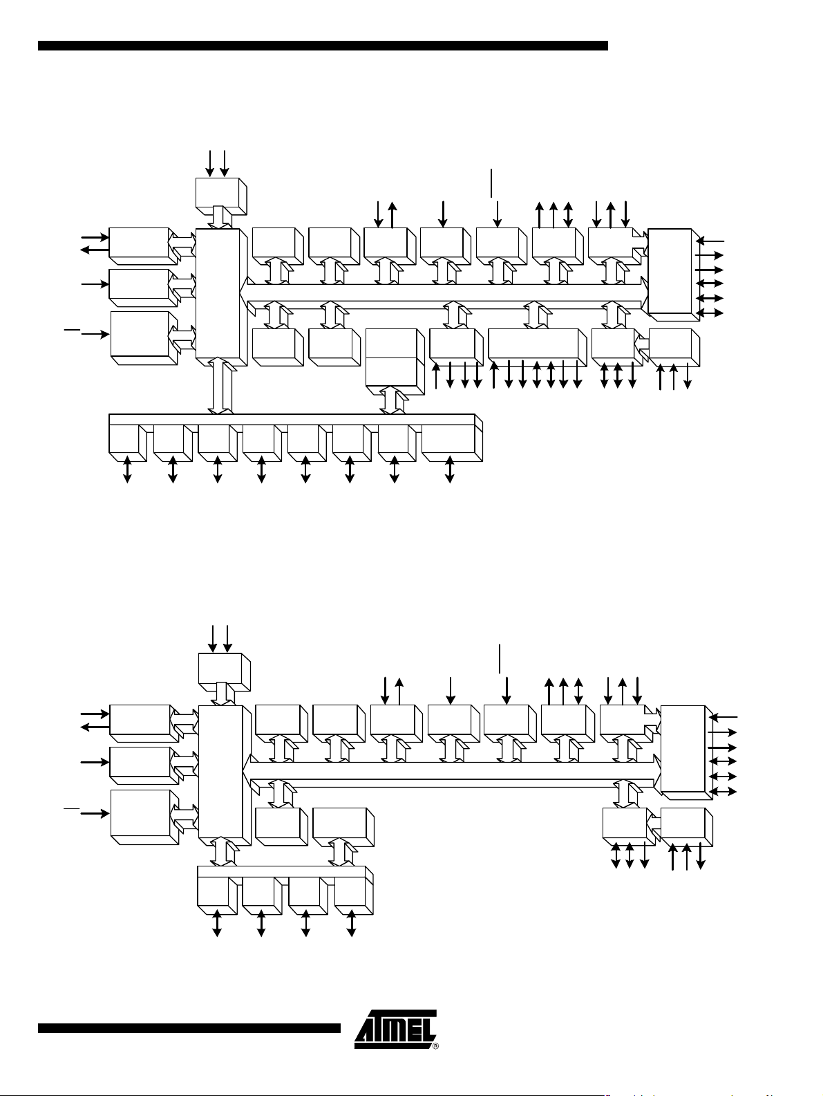
AT8xC5122 Block Diagram
VCC
VSS
AT8xC5122/23
3.3 V
Regulator
XTAL1
XTAL2
RST
8 MHz
Oscillator
PLLPLLF
WATCH-DOG
POR
PFD
RESET
8-BIT
PORT
P0[0-7]
3-BIT
PORT
256 x 8
RAM
80C51 8-BIT CORE
8-BIT
PORT
P1[2,6-7]
P2[0-7]
AT83C5123 Block Diagram
256 x 8
RAM
32K x 8
ROM (1)
Parallel I/O Ports
8-BIT
PORT
P3[0-7]
6-BIT
PORT
512 x 8
XRAM
32K x 8
CRAM (1 )
P4[0-5]
RxD
TxD
UART
Interface
INTERNAL ADDRESS AND DATA BUS
32K x 8
E2PROM (1)
512 x 8
E2PROM (1)
8-BIT
PORT
LED's
P5[0-7]
LED[0-6]
T[0-1]
16-BIT
TIMERS
SPI
Interface
MISO
KBD
Interface
INT[0-1]
Interrupt
Controller
SS
EA
SCK
MOSI
Note 1 : the implementation of these features depends on product versions
KB[0-7]
CRST1
Alternate
Card
External Memory
Controller
ALE
PSEN
AD[0-7]
CCLK1
A[8-15]
LI
CVCC
DC/DC
Converter
USB
Interface
D+
CVSS
ISO 7816
3.3V
Regulator
D-
VREF
AVCC
CIO1
RD
WR
Interface
AVSS
CPRE S
CRST
CCLK
CIO
CC4
CC8
DVCC
XTAL1
XTAL2
RST
8 MHz
Oscillator
PLLPLLF
WATCH-DOG
POR
PFD
RESET
VCC
3.3 V
Regulator
256 x 8
RAM
80C51 8-BIT CORE
3-BIT
PORT
P1[2,6-7]
VSS
Parallel I/O Ports
8-BIT
PORT
256 x 8
RAM
30K x 8
ROM
P3[0-7]
1-BIT
PORT
512 x 8
XRAM
512 x 8
E2PROM (1)
P5.0
LED's
RxD
TxD
UART
Interface
INTERNAL ADDRESS AND DATA BUS
Note 1 : the implementation of these f eatures depends o n pro duct versions
LED[0-3]
T[0-1]
16-BIT
TIMERS
INT[0-1]
Interrupt
Controller
CRST1
CCLK1
Alternate
Card
CIO1
LI
CVCC
DC/DC
Converter
USB
Interface
D+
CVSS
CPRES
CRST
CCL K
ISO 7816
Interface
3.3V
Regulator
D-
VREF
AVSS
AVCC
CIO
CC4
CC8
DVCC
4202E–SCR–06/06
5
Page 6
AT8xC5122/23
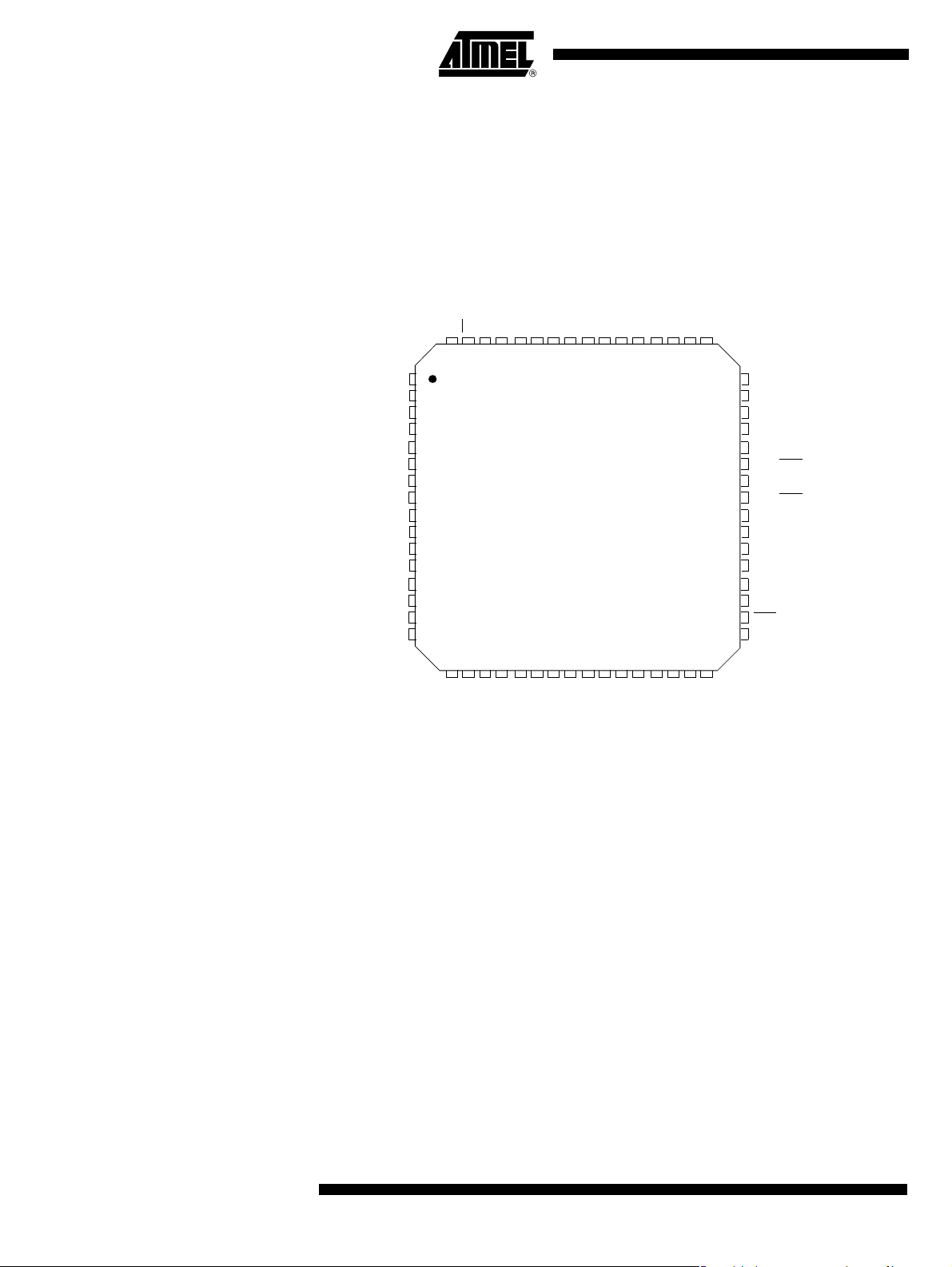
Pinout
High Pin Count Package Description
A T8xC5122 version Figure 1. VQFP64 Package Pinout
D+
P1.7/CCLK1
DVCC
P1.2/CPRES
CC8
P5.7/KB7
P5.6/KB6
CRST
P5.5/KB5
P5.4/KB4
CC4
P5.3/KB3
P5.2/KB2
CCLK
P5.1/KB1
P5.0/KB0
PSEN
VSS
CIO
64 52
1
2
3
4
5
6
7
8
9
10
11
12
13
14
15
16
EA
VREF
62 61 60 59 58 63
D-
P2.1/A9
P2.0/A8
57
56 55 54 53
P2.2/A10
VQFP64
AVCC
PLLF
P2.3/A11
51 50
49
P2.6/A14
P3.1/TxD
48
P1.6/SS
47
P2.7/A15
46
P3.0/RxD
45
P3.5/T1/CRST1
44
P3.2/INT0/LED0/CIO1
43
42
P4.0/MISO
P3.3/INT1
41
P4.1/MOSI
40
P3.4/T0/LED1
39
P4.2/SCK
38
P4.3/LED4
37
P3.6/WR/LED2
36
35
P4.4/LED5
34
RST
33
P4.5/LED6
P2.5/A13
P2.4/A12
AVSS
CVCC
30 29 28 27 26 25 24 23 22 21 20 19 18 17
31 32
LI
ALE
VCC
CVSS
P0.7/AD7
P0.6/AD6
P0.5/AD5
P0.4/AD4
P3.7/RD/LED3
P0.3/AD3
P0.2/AD2
P0.1/AD1
P0.0/AD0
XTAL1
XTAL2
6
4202E–SCR–06/06
Page 7

AT8xC5122/23
Figure 2. PLCC68 Package Pinout (for engineering purpose only)
DVCC
P1.2/CPRES
CC8
P5.7/KB7
P5.6/KB6
CRST
P5.5/KB5
P5.4/KB4
CC4
P5.3/KB3
P5.2/KB2
CCLK
P5.1/KB1
P5.0/KB0
PSEN
VSS
NC
P1.7/CCLK1
EA
CIO
10
11
12
13
14
15
16
17
18
19
20
21
22
23
24
25
26
LI
NC
CVCC
D-
VREF
D+
ALE
VCC
CVSS
P2.2/A10
P2.1/A9
P2.0/A8
AVCC
1686766656463 62 6123456789
PLCC68
35 36 37 38 39 40 41 42 433433323130292827
P0.5/AD5
P0.7/AD7
P0.6/AD6
P0.4/AD4
PLLF
P3.7/RD/LED3
AVSS
P0.3/AD3
P0.2/AD2
P2.3/A11
P2.5/A13
P2.4/A12
P2.6/A14
N/A
N/A
60
P3.1/TxD
59
58
P1.6/SS
P2.7/A15
57
P3.0/RxD
56
55
P3.5/T1/CRST1
54
P3.2/INT0/LED0/CIO1
P4.0/MISO
53
52
P3.3/INT1
P4.1/MOSI
51
P3.4/T0/LED1
50
P4.2/SCK
49
P4.3/LED4
48
P3.6/WR/LED2
47
P4.4/LED5
46
RST
45
P4.5/LED6
44
NC : not connected
XTAL2
P0.1/AD1
XTAT1
P0.0/AD0
N/A : not available
4202E–SCR–06/06
7
Page 8

AT8xC5122/23
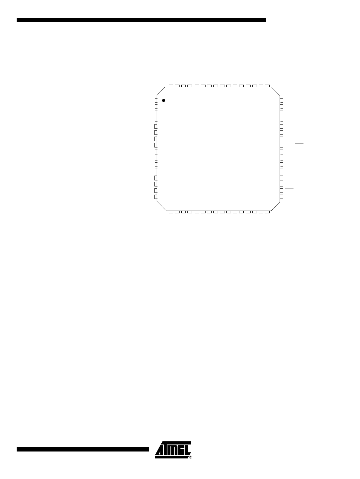
Figure 3. QFN64 Package Pinout
P1.7/CCLK1
DVCC
P1.2/CPRES
CC8
P5.7/KB7
P5.6/KB6
CRST
P5.5/KB5
P5.4/KB4
CC4
P5.3/KB3
P5.2/KB2
CCLK
P5.1/KB1
P5.0/KB0
PSEN
VSS
CIO
64 52
1
2
3
4
5
6
7
8
9
10
11
12
13
14
15
16
EA
VREF
62 61 60 59 58 63
D-
D+
QFN64
P2.1/A9
P2.0/A8
57
56 55 54 53
P2.5/A13
P2.2/A10
AVCC
PLLF
P2.4/A12
AVSS
P2.3/A11
51 50
49
P2.6/A14
P3.1/TxD
48
P1.6/SS
47
P2.7/A15
46
P3.0/RxD
45
P3.5/T1/CRST1
44
P3.2/INT0/LED0/CIO1
43
42
P4.0/MISO
P3.3/INT1
41
P4.1/MOSI
40
P3.4/T0/LED1
39
P4.2/SCK
38
P4.3/LED4
37
P3.6/WR/LED2
36
35
P4.4/LED5
34
RST
33
P4.5/LED6
CVCC
30 29 28 27 26 25 24 23 22 21 20 19 18 17
31 32
LI
ALE
VCC
CVSS
P0.1/AD1
P0.7/AD7
P0.6/AD6
P0.5/AD5
P0.4/AD4
P3.7/RD/LED3
P0.3/AD3
P0.2/AD2
P0.0/AD0
XTAL2
XTAL1
8
4202E–SCR–06/06
Page 9
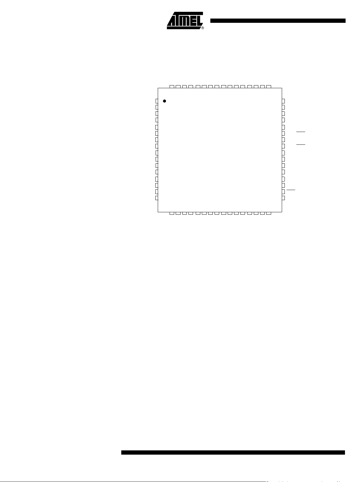
A T89C5122DS version Figure 4. VQFP64 Package Pinout
P1.7/CCLK1
DVCC
P1.2/CPRES
CC8
P5.7/KB7
P5.6/KB6
CRST
P5.5/KB5
P5.4/KB4
CC4
P5.3/KB3
P5.2/KB2
CCLK
P5.1/KB1
P5.0/KB0
PSEN
VSS
CIO
64 52
1
2
3
4
5
6
7
8
9
10
11
12
13
14
15
16
VREF
VCC
D+
62 61 60 59 58 63
P2.2/A10
P2.1/A9
P2.0/A8
D-
57
56 55 54 53
VQFP64
AT8xC5122/23
P2.5/A13
P2.4/A12
AVSS
AVCC
PLLF
P2.3/A11
51 50
49
P2.6/A14
P3.1/TxD
48
P1.6/SS
47
P2.7/A15
46
P3.0/RxD
45
P3.5/T1/CRST1
44
P3.2/INT0/LED0/CIO1
43
42
P4.0/MISO
P3.3/INT1
41
P4.1/MOSI
40
P3.4/T0/LED1
39
P4.2/SCK
38
P4.3/LED4
37
P3.6/WR/LED2
36
35
P4.4/LED5
34
RST
33
P4.5/LED6
CVCC
30 29 28 27 26 25 24 23 22 21 20 19 18 17
31 32
LI
ALE
VCC
CVSS
P0.1/AD1
P0.7/AD7
P0.6/AD6
P0.5/AD5
P0.4/AD4
P3.7/RD/LED3
P0.3/AD3
P0.2/AD2
P0.0/AD0
XTAL2
XTAL1
4202E–SCR–06/06
9
Page 10
AT8xC5122/23
Figure 5. QFN64 Package Pinout
DVCC
P1.2/CPRES
CC8
P5.7/KB7
P5.6/KB6
CRST
P5.5/KB5
P5.4/KB4
CC4
P5.3/KB3
P5.2/KB2
CCLK
P5.1/KB1
P5.0/KB0
PSEN
VSS
VCC
P1.7/CCLK1
CIO
62 61 60 59 58 63
64 52
1
2
3
4
5
6
7
8
9
10
11
12
13
14
15
16
LI
CVSS
CVCC
D-
VREF
D+
ALE
VCC
P0.7/AD7
P2.2/A10
P2.1/A9
P2.0/A8
57
56 55 54 53
QFN64
P0.5/AD5
P0.4/AD4
P0.6/AD6
AVCC
P3.7/RD/LED3
AVSS
PLLF
P2.3/A11
P0.1/AD1
P0.3/AD3
P0.2/AD2
51 50
30 29 28 27 26 25 24 23 22 21 20 19 18 17
49
31 32
XTAL1
P0.0/AD0
P2.6/A14
P3.1/TxD
48
P1.6/SS
47
P2.7/A15
46
P3.0/RxD
45
P3.5/T1/CRST1
44
P3.2/INT0/LED0/CIO1
43
42
P4.0/MISO
P3.3/INT1
41
P4.1/MOSI
40
P3.4/T0/LED1
39
P4.2/SCK
38
P4.3/LED4
37
P3.6/WR/LED2
36
35
P4.4/LED5
34
RST
33
P4.5/LED6
XTAL2
P2.5/A13
P2.4/A12
10
4202E–SCR–06/06
Page 11
Low Pin Count Package Description
AT8xC5122/23
AT8xC5122 and AT83C5123
Figure 6. PLCC28 Package Pinout
versions
DVCC
P1.2/CPRES
CC8
CRST
CC4
CCLK
VSS
5
6
7
8
9
10
11
A T83C5123 version Figure 7. VQFP32 Package Pinout
CIO
D-D+AVCC
VREF
1234282726
PLCC28
15141312 1617 18
LI
VCC
CVSS
CVCC
AVSS
PLLF
P3.1/TxD
25
P3.0/RxD
24
P3.2/INT0/LED0
23
P3.3/INT1
22
P3.4/T0/LED1
21
P3.6/LED2
20
19
RST
XTAL1
XTAL2
P3.7/LED3
DVCC
P1.2/CPRES
CC8
CRST
CC4
CCLK
P5.0
VSS
1
2
3
4
5
6
7
8
CIO
P1.7/CCLK1
VREF
VQFP32
1211109 131415
LI
CVSS
CVCC
D-D+AVCC
28 27 26
VCC
P3.7/LED3
AVSS
PLLF
2529303132
P3.1/TxD
24
P1.6
23
P3.0/RxD
22
P3.5/T1/CRST1
21
P3.2/INT0/LED0/CIO1
20
P3.3/INT1
19
P3.4/T0/LED1
18
P3.6/LED2
17
16
RST
XTAL1
XTAL2
4202E–SCR–06/06
11
Page 12
AT8xC5122/23
Figure 8. QFN32 Package Pinout
DVCC
P1.2/CPRES
CC8
CRST
CC4
CCLK
P5.0
VSS
CIO
P1.7/CCLK1
1
2
3
4
5
6
7
8
LI
CVCC
D-D+AVCC
VREF
28 27 26
QFN32
1211109 131415
VCC
CVSS
P3.7/LED3
AVSS
PLLF
2529303132
P3.1/TxD
24
P1.6
23
P3.0/RxD
22
P3.5/T1/CRST1
21
P3.2/INT0/LED0/CIO1
20
P3.3/INT1
19
P3.4/T0/LED1
18
P3.6/LED2
17
16
RST
XTAL1
XTAL2
12
4202E–SCR–06/06
Page 13

AT8xC5122/23
Pin Descript i on
Table 2. Pin Description
Internal
Power
QFN64
Port
P0.0 30 - 41 - 30 - VCC 2KV I/O Float AD0 P0 KB_OUT Push-pull
P0.1 29 - 40 - 29 - VCC 2KV I/O Float AD1 P0 KB_OUT Push-pull
P0.2 28 - 39 - 28 - VCC 2KV I/O Float AD2 P0 KB_OUT Push-pull
P0.3 27 - 38 - 27 - VCC 2KV I/O Float AD3 P0 KB_OUT Push-pull
P0.4 25 - 36 - 25 - VCC 2KV I/O Float AD4 P0 KB_OUT Push-pull
P0.5 24 - 35 - 24 - VCC 2KV I/O Float AD5 P0 KB_OUT Push-pull
P0.6 23 - 34 - 23 - VCC 2KV I/O Float AD6 P0 KB_OUT Push-pull
P0.7 22 - 33 - 22 - VCC 2KV I/O Float AD7 P0 KB_OUT Push-pull
CIO 64 32 9 4 64 32 CVCC 6KV I/O 0 Port51
VQFP64
VQFP32
PLCC68
PLCC28
QFN32
Supply ESD I/O
Reset
Level Alt
Reset
Config Conf 1 Conf 2 Conf 3 Led
CVCC inactive at reset.
ESD tes ted with a 10µF on CVCC
An external pull-up of 10K is
recommended to support ICC’s
with too high internal pull-ups.
CC4 3 3 12 7 3 3 CVCC 6KV I/O 0 Port51
P1.2 2 2 11 6 2 2 VCC 2KV I/O 1 CPRES Port51
CC4 9 5 18 9 9 5 CVCC 6KV I/O 0 Port51
CCLK 12 6 21 10 12 6 CVCC 6KV O 0 Push-pull
CRST 6 4 15 8 6 4 CVCC 6KV O 0 Push-pull
P1.6 47 23 58 - 47 23 VCC 2KV I/O 1 SS Port51
P1.7 62 31 7 - 62 31 VCC 2KV I/O 1 CCLK1 Port51
P2.0 58 - 3 - 58 - VCC 2KV I/O 1 A8 Port51 Push-pull KB_OUT
P2.1 57 - 2 - 57 - VCC 2KV I/O 1 A9 Port51 Push-pull KB_OUT
P2.2 56 - 1 - 56 - VCC 2KV I/O 1 A10 Port51 Push-pull KB_OUT
P2.3 52 - 65 - 52 - VCC 2KV I/O 1 A11 Port51 Push-pull KB_OUT
CVCC inactive at reset
ESD tes ted with a 10µF on CVCC
Weak & medium pull-u p can be
disconnected
CVCC inactive at reset
ESD tes ted with a 10µF on CVCC
CVCC inactive at reset
ESD tes ted with a 10µF on CVCC
CVCC inactive at reset
ESD tes ted with a 10µF on CVCC
Input
WPU
Input
WPU
Input
WPU
Input
WPU
P2.4 51 - 64 - 51 - VCC 2KV I/O 1 A12 Port51 Push-pull KB_OUT
P2.5 50 - 63 - 50 - VCC 2KV I/O 1 A13 Port51 Push-pull KB_OUT
4202E–SCR–06/06
Input
WPU
Input
WPU
13
Page 14

AT8xC5122/23
Table 2. Pin Description (Continued)
Port
VQFP64
VQFP32
PLCC68
QFN64
PLCC28
Internal
Power
QFN32
Supply ESD I/O
Reset
Level Alt
Reset
Config Conf 1 Conf 2 Conf 3 Led
P2.6 49 - 62 - 49 - VCC 2KV I/O 1 A14 Port51 Push-pull KB_OUT
P2.7 46 - 57 - 46 - VCC 2KV I/O 1 A15 Port51 Push-pull KB_OUT
P3.0 45 22 56 24 45 22 VCC 2KV I/O 1 RxD Port51 Push-pull KB_OUT
P3.1 48 24 59 25 48 24 VCC 2KV I/O 1 TxD Port51 Push-pull KB_OUT
P3.2 43 20 54 23 43 20 VCC 2KV I/O 1 INT0 Port51 LED0
P3.3 41 19 52 22 41 19 VCC 2KV I/O 1 INT1 Port51 Push-pull KB_OUT
P3.4 39 18 50 21 39 18 VCC 2KV I/O 1 T0 Port51 Push-pull KB_OUT
P3.5 44 21 55 - 44 21 VCC 2KV I/O 1 T1 Port51
P3.6 36 17 47 20 36 17 VCC 2KV I/O 1 WR Port51 LED2
P3.7 26 13 37 16 26 13 VCC 2KV I/O 1 RD Port51 LED3
P4.0 42 - 53 - 42 - VCC 2KV I/O 1 MISO Port51
Input
WPU
Input
WPU
Input
WPU
Input
WPU
Input
WPU
Input
WPU
LED1
P4.1 40 - 51 - 40 - VCC 2KV I/O 1 MOSI Port51
P4.2 38 - 49 - 38 - VCC 2KV I/O 1 SCK Port51
P4.3 37 - 48 - 37 - VCC 2KV I/O 1 Port51 Push-pull KB_OUT
P4.4 35 - 46 - 35 - VCC 2KV I/O 1 Port51 Push-pull KB_OUT
P4.5 33 - 44 - 33 - VCC 2KV I/O 1 Port51 Push-pull KB_OUT
P5.0 14 7 23 - 14 7 VCC 2KV I/O 1 KB0 Port51 Push-pull
P5.1 13 - 22 - 13 - VCC 2KV I/O 1 KB1 Port51 Push-pull
P5.2 11 - 20 - 11 - VCC 2KV I/O 1 KB2 Port51 Push-pull
P5.3 10 - 19 - 10 - VCC 2KV I/O 1 KB3 Port51 Push-pull
P5.4 8 - 17 - 8 - VCC 2KV I/O 1 KB4 Port51 Push-pull
Input
MPU
Input
MPU
Input
MPU
Input
WPD
Input
WPD
Input
MPU
Input
MPU
Input
MPU
Input
WPU
Input
WPU
Input
WPU
Input
WPU
Input
WPU
LED4
LED5
LED6
14
4202E–SCR–06/06
Page 15

Table 2. Pin Description (Continued)
Port
VQFP64
VQFP32
PLCC68
QFN64
PLCC28
Internal
Power
QFN32
Supply ESD I/O
Reset
Level Alt
AT8xC5122/23
Reset
Config Conf 1 Conf 2 Conf 3 Led
P5.5 7 - 16 - 7 - VCC 2KV I/O 1 KB5 Port51 Push-pull
P5.6 5 - 14 - 5 - VCC 2KV I/O 1 KB6 Port51 Push-pull
P5.7 4 - 13 - 4 - VCC 2KV I/O 1 KB7 Port51 Push-pull
Reset Input
The Port pins are driven to their reset conditions when a voltage
is applied, whether or not the oscillator is running.
IL
when the chip is in Idle mode or Power-Down mode
Ω
VREF < 3.6 V
can be connected to D+ through a 1.5 KΩ resistor. The V
RST
V
34 16 45 19 34 16 VCC I/0
D+ 60 29 5 2 60 29 DVCC I/O
D- 59 28 4 1 59 28 DVCC I/O
61 30 6 3 61 30 AVCC O
REF
lower than V
This pin has an internal 10K pull-up resistor which allows the device
to be reset by connecting a capacit or between this pi n and VSS.
Asserting RST
returns the chip to normal operation.
The output is active for at least 12 oscillator periods when an internal
reset occurs.
USB Positive Data Upstream Port
This pin requires an external serial resistor of 27Ω (AT8xC122) or
33Ω (AT83C5123) and a 1.5 K
configuration.
USB Negative Data Upstream Port
This pin requires an external serial resistor of 27Ω (AT8xC122) or
33Ω (AT83C5123)
USB Voltage Reference: 3.0 <
V
REF
voltage is controlled by software.
Input
WPD
Input
WPD
Input
WPD
pull-up to VREF for full speed
Input
WPU
Input
WPU
Input
WPU
REF
XTAL
XTAL
VCC
ALE21-32-21- VCC O
31 14 42 17 31 14 VCC I
1
32 15 43 18 32 15 VCC O
2
EA
/
63 - 8 - 63 - VCC I
Input to the on-chip inverting oscillator amplifier
To use the internal oscillator, a crystal or an external oscillator must
be conn ected to this pin.
Output of the on-chip inverting oscillator amplifier
To use the internal oscillator, a crystal circuit must be connected to
this pin. If an external oscillator is used, leave XTAL2 unconnected.
Exter nal Access Enable (Only AT8xC5122)
must be strapped to ground in order to enable the device to fetch
EA
code from external memory locations 0000h to FFFFh.
If security level 1 is programmed, EA
Warning : EA pin cannot be left floating. If the External Access
Enable mod e i s not u se d, EA pi n mus t b e st rapp ed to V CC . I f this l ast
condition is not met,the MCU may have an unpredictable behaviour.
VCC (Only AT89C5122DS)
Address Latch Enable/Program Pulse: Ou tp ut puls e f or latc hing
the low byte of the address during an access to external memory. In
normal operation, ALE is emitted at a constant rate of 1/6 (1/3 in X2
mode) t he os cil lat or f r equ enc y, and can be use d fo r ex ter nal t i mi ng or
clocki ng. Note that one ALE pulse is skipped during each access to
external data memory. ALE can be disabled by setting SFR’s
AUXR.0 bit. With this bit set, ALE will be inactive during internal
fetches
will be latched on reset.
4202E–SCR–06/06
15
Page 16

AT8xC5122/23
Table 2. Pin Description (Continued)
Internal
Power
QFN64
Port
PSEN 15 - 24 - 15 - VCC O
VQFP64
VQFP32
PLCC68
PLCC28
QFN32
Supply ESD I/O
Reset
Level Alt
Program Strobe Enable: The read strobe to external program
memory. When executing code from the external program memory,
PSEN
activations are skipped during each access to external data memory.
PSEN
Reset
Config Conf 1 Conf 2 Conf 3 Led
is activated twice each machine cycle, except that two PSEN
is not activated during fetches from internal program memory.
PLLF 54 26 67 27 54 26 AVCC O
AVCC 55 27 68 28 55 27 PWR
VCC201231152012 PWR
LI 18 10 29 13 18 10 PWR
CVCC 17 9 28 12 17 9 PWR
DVCC 1 1 10 5 1 1 PWR
PLL Low Pass Filter input
Receives the RC network of the PLL low pass filter.
Analog Supply Voltage
AVCC is used to supply the internal 3.3V analog regulator which
supplies the i nternal USB driver
Supply Voltage
VCC is used to supply the internal 3.3V digital regulator which
supplies the PLL, CPU core and internal I/O ’s
DC/DC Input
LI supplies the current for the charge pump of the DC/DC converter.
- LI tied directly to VCC : the DC/DC converter must be configured in
regulator mode.
- LI tied to VC C through an ext ernal 10 µH coil : the DC/DC convert er
can be configured either in regulator or in pump mode.
Card Supply Voltage
CVCC is t he ouput of internal DC/DC co nverter w hich supplies the
Smart Card Interface. It must be connected to an external decoupling
capacitor of 10 µF with the lowest ESR as this parameter influences
on the CVCC noise
Digital Supply V olta ge
DVCC is t he output of the internal analog 3.3V regulator whi c h
supplies the USB driver. This pin must be connected to an external
680nF decoupling capacitor if the USB interface is used.
This ou tpu t ca n be use d by th e ap pl ic ati on w ith a max im um of 10 mA.
CVSS 19 11 30 14 19 11 GND
VSS 16 8 25 11 16 8 GND
AVSS 53 25 66 26 53 25 GND
16
DC/DC Ground
CVSS is used to sink high shunt currents from the external coil
Digital Ground
VSS is used to supply the PLL, buffer ring and the digital core
Analog Ground
AVSS is used to supply the USB driver.
4202E–SCR–06/06
Page 17

Typical Applications
Recommended External components
All the external components described in the figure and table below must be implemented as close as possible from the microcontroller package.
Table 3. External Components Bill Of Materials
Reference Description Value Comments
R1 USB Full Speed Pull-up 1.5 KΩ +/-10% All product versions
AT8xC5122/23
R2 USB pad serial resistor
R3 USB pad serial resistor
R4 PLL filter resis tor 1.8 KΩ +/-10% All product versions
R5 CIO Pull-up resistor 10 KΩ +/10% All product versions
C1 Power Supply filter capacitor 100 nF +80/-20% All product versions
C2 PLL filter capacitor 33 pF +/-10% All product versions
C3 PLL filter capacitor 150 pF +/-10% All product versions
C4 USB pad decoupling c apacitor 680 nF +/-30%
C5 Smart Card clock filter capacitor 27 pF +/-10% All product versions.
C6 DC/DC Converter decoupling capacitor
C7 DC/DC Converter filter capacitor 100 nF +80/-20% All product versions
C8 Power Supply decoupling capacitor 4.7 µF +/-10%
27 Ω +/-10% For AT8xC 5122 versions
33 Ω +/-10% For AT83C5123 versions
27 Ω +/-10% For AT8xC 5122 versions
33 Ω +/-10% For AT83C5123 versions
All product versions.
If USB interface is not used, this capacitor is optional
10 µF +/-10%
Low ESR
All product versions.
This capacitor does not impact the USB Inrush Current
All products versions
This capacitor impacts the USB Inrush Current. Maximum
application capacitance allowed by the USB standard is 10 µF.
C9 Power Supply filter capacitor 100 nF +80/-20C All product versions
C10 Reset capa citor 10 µF +/-10% Option al capacitor for all produ c t versio ns
L1 DC/DC converter input inductance
Q1 Crystal
10 µH +/- 1 0%
Min rated current : 200 mA
Min rated freq. : 4 MHz
8.0000 Mhz +/- 2500 ppm
max
ESR max : 100 Ω
All product versions.
Qualified component : Murata LQH32CN100K21L
If DC/DC converter is not used at 5V, this inductance is optional.
All product versions
4202E–SCR–06/06
17
Page 18
AT8xC5122/23
USB Keyboard with Smart Card Reader Using the AT8xC5122 and AT89C5122DS Versions
VCC
C9
GND
VCC
EA/VCC (1)
10mA Max
GND
R1
R2
R3
R19
R18
R17
R16
R15
D+
D-
VCC
GND
R14
R13
R12
R11
R10
R09
R08
USB
VBUS
GND
R07
R06
R05
R04
R03
R02
R01
R00
C4
C0
C1
C2
C3
C4
C5
C6
C7
DVCC
VREF
D+
D-
KB0
KB1
KB2
KB3
KB4
KB5
KB6
KB7
P3[0-1,3-4]
P2[0-7]
P0[0-7]
GND
VCC AVCC
C8
VCC
CPRES
CRST1
CCLK1
GND
LEDx
CVCC
CVSS
CRST
CCLK
CC4
CIO
CC8
CIO1
C1
VCC
C7
R5
VCC
VCC
Smart Card
C1
VCC
C5
GND
C2
RST
C3
CLK
C4
C4
C7
I/O
C8
C8
S1
S1
S2
GND
L1
LI
C6
GND
Alternate Card
C1
VCC
C2
RST
C3
CLK
C7
I/O
C5
GND
GND
Keyboard Matrix
Notes :
1 - Pin configuration depends on product versions
18
R4
C3
GND
C2
PLLF
AVSS
VSS
GND
XTAL2XTAL1
Q1
RST
C10
Optional
Capacitor
GND
4202E–SCR–06/06
Page 19
USB Smart Card Reader Using the AT83C5123 Version
AT8xC5122/23
USB
VBUS
D+
GND
D-
VCC
GND
VCC
10mA Max
GND
R1
R2
R3
C4
C9
VCC
GND
EA
DVCC
VREF
D+
D-
GND
VCC AVCC
C8
VCC
CVCC
CPRES
GND
LEDx
CVSS
CRST
CCLK
CC4
CIO
CC8
C1
VCC
VCC
L1
LI
C6
GND
C7
R5
Smart Card
C1
VCC
C5
GND
C2
RST
C3
CLK
C4
C4
C7
I/O
C8
C8
S1
S1
S2
GND
R4
C3
GND
C2
PLLF
AVSS
VSS
GND
CRST1
CCLK1
CIO1
RST
XTAL2XTAL1
Q1
C10
GND
VCC
GND
Optional
Capacitor
Alternate Card
C1
VCC
C2
RST
C3
CLK
C7
I/O
C5
GND
4202E–SCR–06/06
19
Page 20
AT8xC5122/23
Memory Or ga nization The AT8xC5122/23 devices have separated address spaces for Program and Data
Memory, as shown in Figure 13 on page 29, Figure 14 on page 31 and Figure 15 on
page 32. The logical separation of Program and Data memory allows the Data Memory
to be accessed by 8-bi t addresses , which can be more quic kly stored and m anipulate d
by an-bit CPU. Nevertheless, 16-bit Data Memory addresses can also be generated
through the DPTR register.
Program Memory Managament
Depending on the state of EA pin, the MCU fetches the code from internal or external
progr am memory (R OMless mod e )
Warning : the EA pin c an not be lef t flo ating , oth er wise M CU m ay have an unpr ed ictable behaviour.
If EA is strapped to VCC, the MCU fetches the code from the internal program memo ry.
The wa y th e MC U works in this mod e depe nds o n the d evic e ve rsi on. S ee next pa ragraphs for further details.
If the EA is strapped to GND, the MCU fetches the code from external program memory.
This mode is common for all device versions wich supports it. After reset, the CPU
begins the execution from location 0000h. There can be up to 64 KBytes of program
memory. In this mode, the internal program memories are disabled.
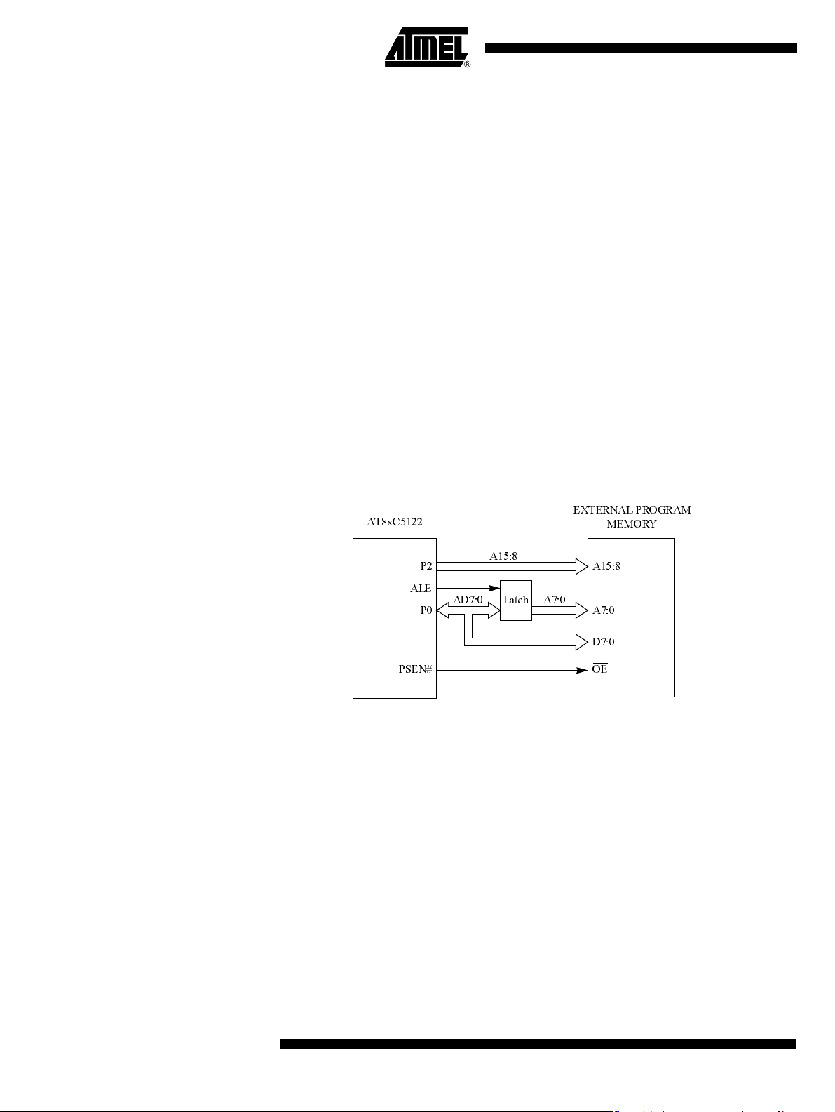
The hardware configuration for external program execution is shown in Figure 9.
Figure 9. Executing from External Program Memory
AT8xC5122
ALE
P2
P0
AD7:0
A15:8
Latch
EXTERNAL PROGRAM
MEMORY
A15:8
A7:0
A7:0
20
D7:0
OEPSEN#
Note that the 16 I/O line s (Ports 0 and 2) are dedicated to bus func tions during ex ternal
Program Mem ory fetches. P ort 0 serves a s a m ultiplexed a ddre ss/dat bus. It em its the
low byte of the Program Counter (PC L) as an add ress, and then go es into a floa t state
awaiting the arrival of the code byte from the Program Mem ory . During the time that the
low byte of the Program Counter is valid on P0, the signal ALE (Address Latch Enable)
clocks the byte into an address latch. Meanwhile, Port 2 emits the high byte of the Program Counter (PCH). Then PSEN strobes the External Program M emory and the code
byte is read into the MCU.
PSEN is not activated and Ports P0 and P2 are not affected during internal program
fetches.
4202E–SCR–06/06
Page 21

AT8xC5122/23
Data Memory Managament
RAM Achitecture The internal RAM is mapped into three separate segments :
All device versions implements :
- 256 Bytes of RAM to increase data parameter handling and high level language usage
- 512 bytes of XRAM (Extended RAM) to store program data.
• The Lower 128 bytes (addresses 00h to 7Fh) are directly and indirectly
addressable.
• The Upper 128 bytes (addresses 80h to FFh) are indirectly addressable only.
• The Special Function Registers (SFRs) (addresses 80h to FFh) are directly
addressable only.
The U pper 12 8 bytes and SF R’s ha ve the same address spac e but ar e phys ically
separated.
When an instruction ac cesses an i nternal location ab ove addres s 7Fh, the CPU knows
whether the ac cess is in the upper 128 b ytes of data RA M or to SFR space by the
addressing mode used in the instruction.
• Instructions that use direct addressing access SFR space. For example: MOV
0A0H, # data, accesses the SFR at location 0A0h (which is P2).
• Instructions that use indirect addressing access the Upper 128 bytes of data RAM.
For example: MOV @R0, # data where R0 contains 0A0h, accesses the data byte
at address 0A0h, rather than P2 (whose address is 0A0h).
The stack pointer (SP) may be locat ed anywhere in the 256 bytes RAM (lowe r and
upper RAM) internal data memory. The stack may not be located in the XRAM.
The M0 bit al lows to st retc h the X RA M ti mings . If M 0 is s et, t he re ad an d w rite pu ls es
are extended from 6 to 30 clock periods. This is useful to access externa l slow
peripherals.
XRAM Achitecture Depending on the state of EXTRAM bit in AUXR register (See Table 5 on p age 24), t he
MCU fetches data from internal or external XRAM.
If EXTRAM=0 (reset condition), the MCU fetches the data from internal XRAM. The size
of internal XRAM is configured by the bit XRS0 in AUXR register (See Table 5 on page
24).
Table 4. XRAM Size Configuration
Address
XRS0 XRAM size
0
1 512 bytes 000h 1FFh
The XRAM logically occupie s the first bytes of external data memory. The bit XRS0 can
be used to hide a part of the available XRAM . This can be use ful if external peripherals
are mapped at addresses already used by the internal XRAM.
The XRAM is indirectly addressed, using the MOVX instruction in combination with any
of the registers R0, R1 of the selected bank or DPTR.
256 Bytes
(Reset condition)
Start End
000h 0FFh
4202E–SCR–06/06
For example, MOVX @R0, # data where R0 contains 0A0H, accesses the XRAM at
address 0A0H rather than external memory.
21
Page 22
AT8xC5122/23
An access to e xternal XRAM m emory locations hig her than the accessi ble size o f the
memory (roll-over feature) will be performed with the M OVX DPTR i nstructions, with P 0
and P2 as data/address busses, WR
and RD as respectively write and read signals.
Accesses above XRAM size can only be done by the use of DPTR.
If EXTRAM=1 the MCU fetches the data from external XRAM Memory. There can be up
to 64 KBytes of external XRAM Memory.
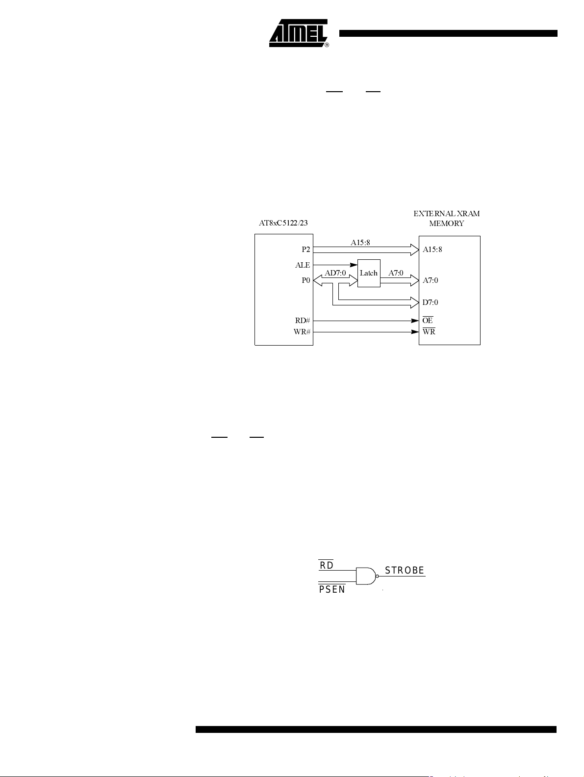
The hardware configuration for external Data Memory Access is shown in Figure 10
Figure 10. Accessing to External XRAM Memory
AT8xC5122/23
EXTER NAL XRAM
MEMORY
AD7:0
A15:8
Latch
A7:0
A15:8
A7:0
D7:0
OERD#
WR
P2
ALE
P0
WR#
MOVX @Ri an d M OVX @DPT R wil l be similar to the standard 80C51. MOVX @ Ri will
provide an eight-bit address multiplexed with data on Port 0 and any output port pins
can be use d to ou tput hi gher ord er addre ss bi ts. Thi s is to p rovide t he ext ernal pagin g
capability. MO VX @DP TR will generate a sixteen -bit addre ss. Po rt 2 outputs the highorder eight address bits (DPH) while Port0 m ultiplexes the low -order eight address bits
(DPL) with data. MOVX @ Ri a nd M OVX @DPTR will generate either read or write signals on W
R and RD.
Ports P0, P2 are not affected and RD, WR signals are not activated during access to
internal XR AM.
Note that external XRAM Memory access is only available on High Pin Count Packages.
External Program Memory and ext ernal XRAM Memory may be combined if desired by
applying the RD and PSEN sig nals t o the in puts o f a n AND gat e and using the ouput of
the gate as the read strobe to the external program/data memory.
Dual Data Pointer Register (DDPTR)
22
RD
STROBE
PSEN
The addi tion al da ta poin ter ca n be u sed t o spe ed up code exe cuti on and reduc e cod e
size.
The dual DPTR structure is a way by which the chip will specify the address of an external data memory location. There are two 16-bit DPTR registers that address the external
memory, and a single bit called DPS = AUXR1.0 (see Table 7) that allow the program
code to switch between them (Figure 11).
4202E–SCR–06/06
Page 23
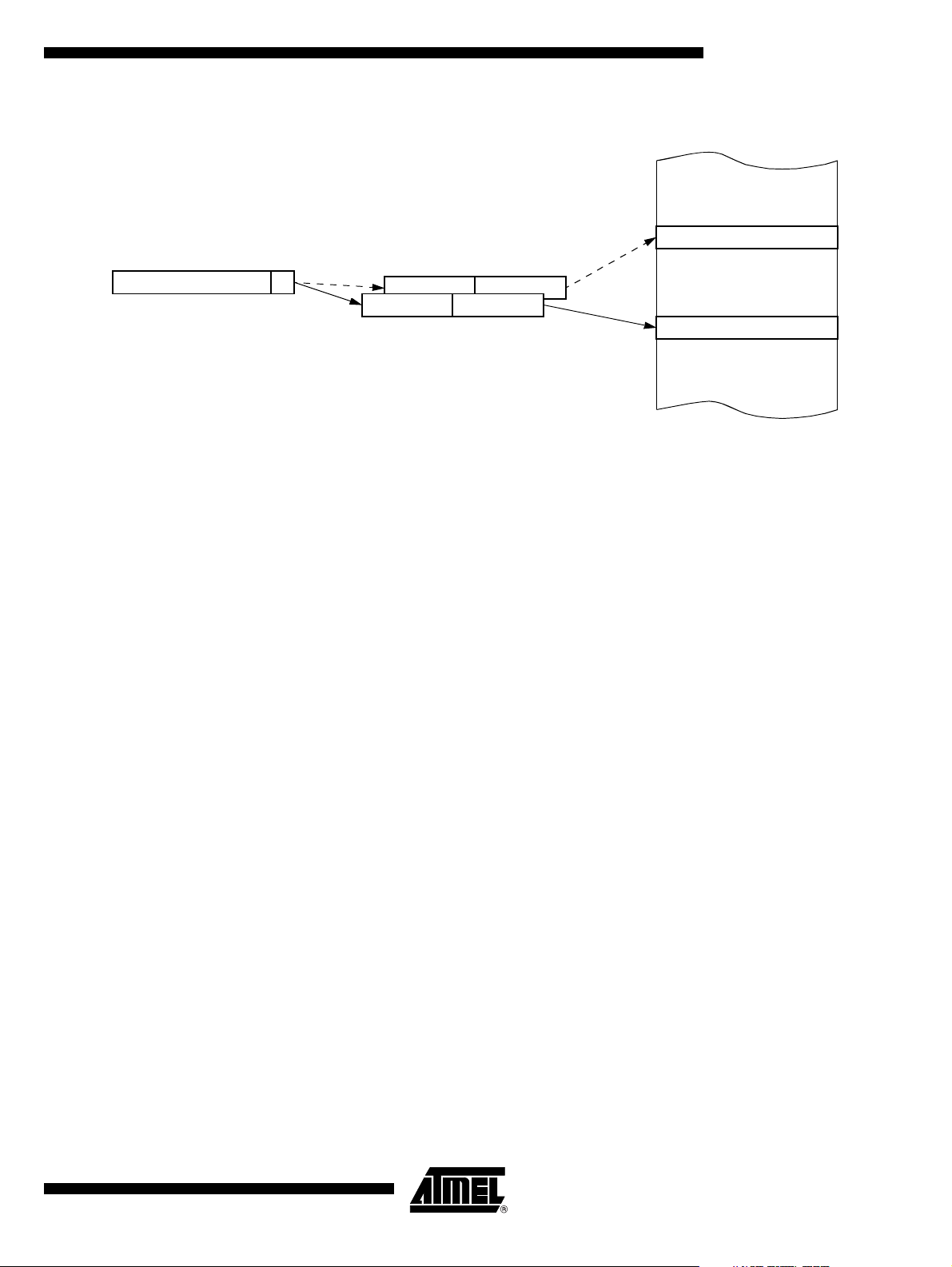
Figure 11. Use of Dual Pointer
AUXR1(A2H)
Assembly Language
AT8xC5122/23
External Data Memory
07
DPS
DPH(83H) DPL(82H)
a. Bit 2 stuck at 0; this allows to use INC AUXR1 to toggle DPS without changing GF3.
; Block move using dual data pointers
; Modifies DPTR0, DPTR1, A and PSW
; note: DPS exits opposite of entry state
; unless an extra INC AUXR1 is added
;
00A2 AUXR1 QU 0A2H
;
0000 909000MOV DPTR,#SOURCE ; address of SOURCE
0003 05A2 INC AUXR1 ; switch data pointers
0005 90A000 MOV DPTR,#DEST ; address of DEST
0008 LOOP:
0008 05A2 INC AUXR1 ; switch data pointers
000A E0 MOVX A,@DPTR ; get a byte from SOURCE
000B A3 INC DPTR ;increment SOURCE address
000C 05A2 INC AUXR1 ; switch data pointers
000E F0 MOVX @DPTR,A ; write the byte to DEST
000F A3 INC DPTR ; increment DEST address
0010 70F6JNZ LOOP ; check for 0 terminator
0012 05A2 INC AUXR1 ; (optional) restore DPS
DPTR1
DPTR0
4202E–SCR–06/06
INC is a short (2 bytes) and fast (12 clocks) way to manipulate the DPS bit in the AUXR1
SFR. However, note that the INC instruction does not directly force the DPS bit to a particular state, but simply toggl es it. In simple rou tines, such as the block move example,
only the fact that DPS is toggled in the proper sequence matters, not its actual value.
For example, the block move routine works the sam e whether DPS is '0' or '1 ' on ent ry.
Observe that witho ut the last ins truction (INC AUXR1), th e routine will exit with DP S in
the opposite state.
23
Page 24

AT8xC5122/23
Registers
Table 5. Auxiliary Register - AUXR (8Eh)
76543210
DPU - - - XRS0 EXTRAM AO
Bit
Number
7DPU
6-3 -
2XRS0
1 EXTRAM
0AO
Bit
Mnemonic Description
Disable weak Pull-up
0 weak pull-up is enabled
1 weak pull-up is disabl ed
Reserved
The value read from this bit is indeterminate. Do not change these bits.
XRAM Size
0 256 bytes (default)
1 512 bytes
EXTRAM bit
Cleared to access internal XRAM using MOVX @ Ri/ @ DPTR.
Set to access external memory.
Programmed by hardware after Power-up regarding Hardware Security Byte
(HSB), default setting , XRAM selected.
ALE Output bit
Cleared , ALE is emitted at a constant rate of 1/6 the o s cillator frequency (or 1/3 if
X2 mode is used)( default).
Set , ALE is active only when a MOVX or MOVC instruction is used.
Reset Value = 0XXX X000b
24
4202E–SCR–06/06
Page 25
AT8xC5122/23
Table 6. Auxiliary Register 1 AUXR1- (0A2h) for AT8xC5122
7 6 5 4 3 2 1 0
--ENBOOT-GF30-DPS
Bit
Number
7 - 6 -
5 ENBOOT
4-
3 GF3 This bit is a general-purpose user flag.
2 0 Always cleared .
1-
0DPS
Bit
Mnemonic Description
Reserved
The valu e re a d from this bit is ind et er m in at e. Do not chang e th es e bits .
Enable Boot ROM (CRAM / E2PROM version only)
Set this bit to map the Boot ROM from 8000h to FFFFh. If the PC increments
beyond 7FFFh address, the code is fetch from int ernal ROM
Clear this bit to disable Bo ot ROM. If the PC increments beyond 7FFF h address,
the code is fetch from external code memory (C51 standard roll over function)
This bit is forced to 1 at reset
Reserved
The value rea d fro m thi s bit is ind et erm in at e. Do no t chang e th is bit.
Reserved
The value rea d fro m thi s bit is ind et erm in at e. Do no t chang e th is bit.
Data Pointer Selection
Cleared to select DPTR0. Set to select DPTR1.
Reset Value = XX1X XX0X0b (Not bit addressable)
Table 7. Auxiliary Register 1 AUXR1- (0A2h) for AT83C5123
7 6 5 4 3 2 1 0
----GF30-DPS
Bit
Number
7 - 6 -
5
4-
3 GF3 This bit is a general-purpose user flag.
2 0 Always cleared .
1-
0DPS
Bit
Mnemonic Description
Reserved
The valu e re a d from this bit is ind et er m in at e. Do not chang e th es e bits .
Reserved
The valu e re a d from this bit is ind et er m in at e. Do not chang e th es e bits .
Reserved
The value rea d fro m thi s bit is ind et erm in at e. Do no t chang e th is bit.
Reserved
The value rea d fro m thi s bit is ind et erm in at e. Do no t chang e th is bit.
Data Pointer Selection
Cleared to select DPTR0.
Set to select DPTR1.
Reset Value = XXXX XX0X0b (Not bit addressable)
4202E–SCR–06/06
25
Page 26

AT8xC5122/23
Table 8. CRAM Configuration Register - RCON (D1h)
76543210
----RPS---
Bit
Number
7 - 4 -
3RPS
2-0 -
Bit
Mnemonic Description
Reset Value = XXXX 0XXXb
AT8xC5122’s CRAM and E2PROM Versions
The AT8xC5122’s CRAM and E2PROM versions implements :
- 32 KB of ROM mapped from 8000 to FFFF in which is embed ded a bootlo ader for In-
System Programming feature
- 32 KB of CRAM (Code RAM) , a volatile program memory mapped from 0000 to 7FFF
In CRAM versions only :
- 512 bytes of E2PROM can be optionally implemented to store permane nt data
Reserved
The value read from this bit is indeterminate. Do not change these bits.
CRAM Memory Mapping Bit
Set to map the CRAM memory during MOVX instructions
Clear to map the XRAM memory during MOVX .
This bit has priority over th e EXTRAM bit.
Reserved
The value read from this bit is indeterminate. Do not change these bits.
In E2PR OM ver sion :
- 32KB of E2PROM are implemented to store permanent code
Warnings :
– so me bytes of user program memory space are reserved for bootloader
configuration. Depending on the configuration, up to 256 bytes of code may
be not available for the user code from 7F00h location. Refer to bootloader
datasheet for further details.
– Port P3.7 may be used by the bootloader as a hardware condition at reset to
select the In-System Programming mode. Once the bootloader has started,
the P3.7 Port is no more used.
26
4202E–SCR–06/06
Page 27
AT8xC5122 Microcontroller
FFFFh
Bootloader
AT8xC5122/23
P3.7
7FFFh
7F00h
7EFFh
0000h
When pin EA =1 and after the reset, the MCU begins the execution of the embedded
bootloade r from loca tion F8 00h of the ROM. T he b ootload er implem ent s an In-Sys tem
Programming (ISP) mode which manages the transfer of the code in the volatile Program Memory (CR A M) .
For CRAM ve rsion, th e code is sup plied b y the ATME L’s FL exible In-system Pro gramming software (FLIP) through USB or UART interface
For E2PROM vers ion, t he code is supplied from the internal cod e E2P ROM or by F LI P.
The s tate of pi n P 3.7 at re set de term ines the code so urc e. I f P3 .7=1 (re set cond ition )
the source is the internal E2PROM and the transfer takes about 1.5 seconds. If P3.7=0
the source is FLIP and the transfer time depends mainly on external conditions not
related to bootloader.
Reserved
User code
4202E–SCR–06/06
Once the code is running in CRAM, the roll-over condition (code fetched beyond
address 7FFFh) depends on the state of ENBOOT bit of AUXR1 register (Table 6 on
page 25).
If ENBOOT=1 (reset condition) the MCU fetche s the code from bootloader ROM. If
ENBOOT=0, the MCU fetches the code from the external Program Memory. In this last
case, PSEN is activated and Ports P0 and P2 are used to emit data and address
signals.
Warning : external Program Memory access is not allowed on Low Pin Count
Packages.
27
Page 28
AT8xC5122/23
Using CRAM Memory The CRAM is a read / write volatile memory that is mapped in the program memory
space. Then wh en the p ower is sw itched off t he code is l ost and ne eds to be reload at
each power up. In return, the CRAM enabl es a lot of f lexibility in the code dev elopment
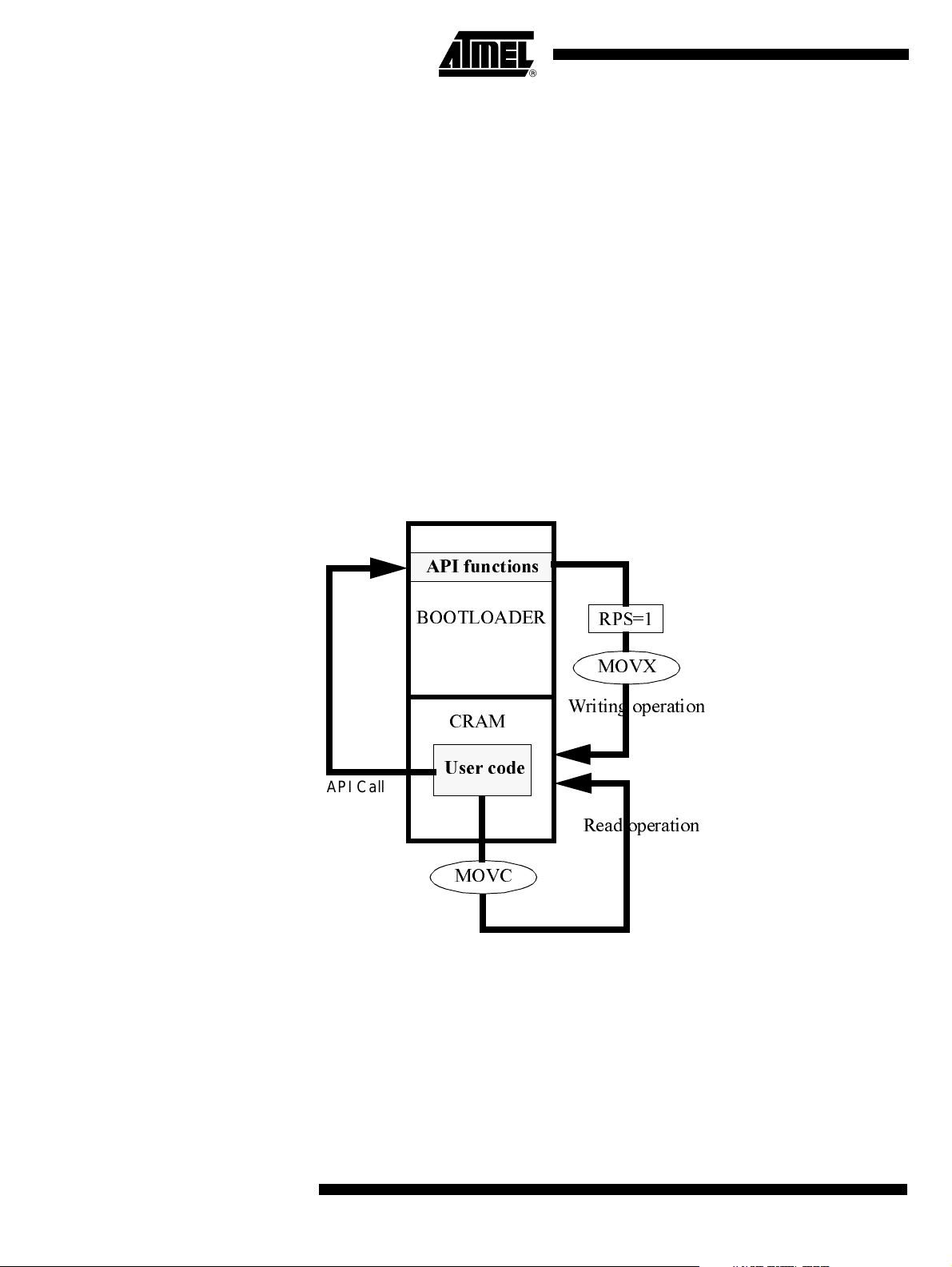
as it can be programm ed indefinite ly. The user code runnin g in the CRAM c an perform
read operations in CRAM itself by means of MOVC instructions like any C51 m icrocontroller does. Although the writing operations in CRAM are usually handled by the
bootloader, it is possible for the user code to handle its own writing operations in CRAM
as well. The user co de must c all API functi ons prov ide d by th e bootlo ade r in the R OM
memory. Refer to bootloader datasheet for further details about the use of these API
functions. These API functions use a mechanism provided by the AT8xC5122 microcontroller. When the bit RPS is set in RCON register (Tabl e 8 on page 26), the MOVX
intructions are configured to write in CRAM instead of XRAM m em ory. Ho wever, due t o
C51 architecture, it is not possible for the user c ode to write directly in CRAM when it is
itself running in CRAM. This is why the API functions must be called in order to have the
code executing in ROM while the CRAM is written.
Figure 12. Read / Write Mechanisms in CRAM Memory
API Call
API functions
BOOTLOADER
CRAM
User code
MOVC
RPS=1
MOVX
Writing operation
Read operation
28
4202E–SCR–06/06
Page 29
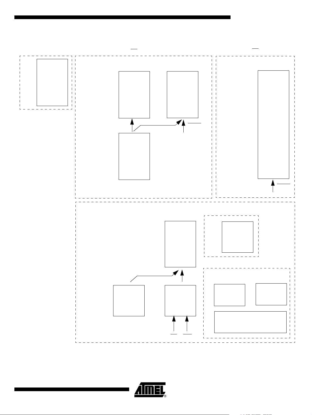
Figure 13. AT8xC5122’s CRAM and E2PROM Versions
AT8xC5122/23
(E2PROM version)
FFFF
32K
INTERNAL
E2PROM
(Read/Write)
8000
PROGRAM
MEMORY
Reset@
FFFF
<F800>
8000
Roll-Over
7FFF
0000
EA = 1
ENBOOT=1
32K
INTERNAL
ROM
(Read Only)
32K
INTERNAL
CRAM
(Read/Write)
FFFF
8000
ENBOOT=0
32K
EXTERNAL
PROGRAM
MEMORY
PSEN
Reset@
EA = 0
EXTERNAL
PROGRAM
MEMORY
<0000>
PSEN
DATA MEMORY
(Read / Write)
01FF
0000
EXTRAM=0
Roll-Over
On-chip
512 bytes
XRAM
FFFF
0200
01FF
0000
EXTRAM=1
EXTERNAL
XRAM
EXTERNAL
XRAM
RD WR
Optional
(applicable only to CRAM version)
01FF
512 Bytes
INTERNAL
E2PROM
0000
On-Chip 256 bytes RAM
Indirect
Addressing
FF
128 Bytes
80
7F
00
Upper
RAM
128 Bytes
Direct
Addressing
FF
SFR
Space
80
Lower
RAM
4202E–SCR–06/06
29
Page 30

AT8xC5122/23
AT8xC5122’s ROM Version
Security Level There are two security levels (applicable to High Pin Count packages only) :
The AT8xC5122’s ROM version implements :
- 32 K of ROM mappe d fro m 0 000h to 7FFFh in which is em bedded the user code. The
ROM device is only factory programmable.
- 512 byte s of E 2P ROM can be op tiona lly imp lem ente d to s tore pe rman en t data. Wi th
this option, the size of ROM is reduced to 30K.
After the rese t, th e MCU b egins t he exe cutio n of the user code fr om lo cation 00 00 h of
the ROM.
Access to external Program Memory is not allowed.
Table 9. Security Level s Des cri ption
Securi ty Level Prote ction description
1 No protection lock enabl ed
MOVC instruction executed from external Program Memory is disabled when fe tching
2
code bytes from internal Program Memory
EA
is sampled and latched on r eset.
External code execution is enabled.
The security level 2 can be used to protect the user code from piracy. This option is configured at factory and must be requested by the customer at order time.
30
4202E–SCR–06/06
Page 31

Figure 14. AT8xC5122’s ROM Version
AT8xC5122/23
PROGRAM MEMORY
(Read only)
7FFF
0000
EA=1
Roll-Over
INTERNAL
32K ROM
EXTRAM=0
FFFF
8000
RESET@
<0000>
EA=0
EXTERNAL
EXTERNAL
PSEN
EXTRAM=1
Optional
DATA MEMORY
(Read / Write)
01FF
0000
On-chip
512 bytes
XRAM
FFFF
0200
Roll-Over
01FF
0000
EXTERNAL
XRAM
EXTERNAL
XRAM
RD WR
01FF
512 Bytes
INTERNAL
E2PROM
0000
On-Chip 256 bytes RAM
Indirect
Addressing
FF
80
7F
00
Upper
128 Bytes
RAM
FF
80
Lower
128 Bytes
RAM
Direct
Addressing
SFR
Space
4202E–SCR–06/06
31
Page 32

AT8xC5122/23
AT83C5123 Version The AT83C5123 device is a low pin count version of the AT8xC5122.
The ROM version implements :
- 30 KB of ROM mapp ed from 0000 t o 77 FF in w hich is em bedded the user co de. Th e
ROM device is only factory programmable.
- 512 bytes of E2PROM can be optionally implemented to store permane nt data
Figure 15. AT83C5123’s Device
7FFF
PROGRAM MEMORY
(Read only)
DATA MEMORY
(Read / Write)
RESET@
<0000>
OPTIONAL
01FF
0000
01FF
0000
INTERNAL
30K ROM
512 Bytes
INTERNAL
E2PROM
On-chip
512 bytes
XRAM
On-Chip 256 bytes RAM
Indirect
Addressing
FF
80
7F
00
Upper
128 Bytes
RAM
FF
80
Lower
128 Bytes
RAM
Direct
Addressing
SFR
Space
32
4202E–SCR–06/06
Page 33

AT8xC5122/23
Special Function Register s (S FR ’s)
Introduction The Special Function Registers (SFRs) of the AT8xC5122/23 can be ranked into the fol-
lowing categories:
• C51 Core Registers: ACC, B, DPH, DPL, PSW, SP
• System Configuration Registers: PCON, CKRL, CKCON0, CKCON1, CKSEL,
PLLCON, PLLDI V, AUXR, AUXR1, RCON
• I/O Port Registers: P0, P1, P2, P3, P4, P5, PMOD1, PMOD2
• Timer Registers: TCON, TH0, TH1, TMOD, TL0, TL1
• Watchdog (WD) Registers: WDTRST, WDTPRG
• Serial I/O Port Registers: SADDR, SADEN, SBUF, SCON
• Baud Rate Generator (BRG) Registers: BRL, BDRCON
• System Interrupt Registers: IE0, IPL0, IPH0, IE1, IPL1, IPH1
• Smart Card Interface (SCI) Registers: SCSR, SCCON/SCETU0, SCI SR/SCETU1,
SCIER/SCIIR, SCIBUF, SCGT0/SC WT0 , SCGT1/SCWT1, SCICR/SC WT2 , SCIC L K
• DC/DC Converter Registers: DCCKPS
• Keyboard Interface Registers: KBE, KBF, KBLS
• Seri a l Port Int erface (SPI) Reg i s ters: SP C ON, SPS TA, SPDAT
• Universal Serial Bus (USB) Registers:USBCON, USBADDR, USBINT, USBIEN,
UEPNUM, UEPCONX, U EPSTAX, UEPRST, UEPINT, UEPIEN, UEPD ATX,
UBYCTX, UFNUML, UFNUMH
• LED Controller Registers: LEDCON0, LEDCON1
4202E–SCR–06/06
33
Page 34

AT8xC5122/23
AT8xC5122 V er sio n
Bit
addressable Not bit addressable
0/8 1 /9 2/A 3/B 4/ C 5/D 6/E 7/F
F8h
F0h
E8h
E0h
UEPINT
0000 0000
B
0000 0000
P5
1111 1111
ACC
0000 0000
LEDCON0
0000 0000
LEDCON1
XX00 0000
UBYCTX
0000 0000
D8h
D0h
PSW
0000 0000
C8h
1
S
C
C0h
R
S
0
B8h
1
S
C
B0h
R
0
S
1
S
C
A8h
R
S
0
P4
1111 1111
IPL0
X000 000
P3
1111 1111
IEN0
0000 0000
RCON
XXXX 0XXX
SCICLK
(1)
0X10 1111
(1)
SCWT3
0000 0000
SADEN
0000 0000
IEN1
XXXX X000
SADDR
0000 0000
UEPIEN
0000 0000
UFNUML
0000 0000
IPL1
00XX 00X0
SCIBUF
XXXX XXXX
SPCON
0001 0100
UFNUMH
0000 0000
IPH1
00XX 00X0
SCSR
X000 1000
UEPCONX
1000 0000
SPSTA
0000 0000
USBCON
0000 0000
SCGT0
0000 1100
SCWT0
1000 0000
SCETU0
0111 0100
SCCON
0000 0000
(1)
(1)
(1)
(1)
UEPRST
0000 0000
SPDAT
1111 1111
USBINT
0000 0000
(1)
SCGT1
XXXX XXX0
(1)
SCWT1
0010 0101
SCETU1
(1)
XXXX X001
(1)
SCISR
10X0 0000
UEPSTAX
0000 0000
USBADDR
1000 0000
USBIEN
0000 0000
(1)
SCICR
0000 0000
SCWT2
0000 0000
(1)
SCIER
0X00 0000
(1)
SCIIR
0X00 0000
UEPDATX
0000 0000
UEPNUM
0000 0000
DCCKPS
0000 0000
IPH0
(1)
X000 0000
A0h
98h
90h
88h
80h
P2
1111 1111
SCON
0000 0000
P1
1111 1111
TCON
0000 0000
P0
1111 1111
34
ISEL
0000 0100
SBUF
XXXX XXXX
(2)
PMOD0
0000 0000
TMOD
0000 0000
SP
0000 0111
Notes: 1. Mapping is done using SCRS bit in SCSR register.
AUXR1
XX1X 0XX0
BRL
0000 0000
TL0
0000 0000
DPL
0000 0000
PLLCON
XXXX X000
BDRCON
XXX0 00 00
TL1
0000 0000
DPH
0000 0000
2. Grey areas : do not write in .
PLLDIV
0000 0000
KBLS
0000 0000
TH0
0000 0000
PMOD1
0000 0000
KBE
0000 0000
TH1
0000 0000
CKSEL
XXXX XXX0
WDTRST
XXXX XXXX
KBF
0000 0000
AUXR
0XXX X000
WDTPRG
XXXX X000
CKRL
XXXX 1111
CKCON0
X0X0 X000
PCON
00X1 0000
4202E–SCR–06/06
Page 35

AT83C5123 V er sio n
Bit
addressable Not bit addressable
0/8 1/9 2/A 3/B 4/C 5/D 6/E 7/F
AT8xC5122/23
F8h
F0h
E8h
E0h
UEPINT
0000 0000
B
0000 0000
P5
XXXX XXX1
ACC
0000 0000
LEDCON0
0000 0000
UBYCTX
0000 0000
D8h
D0h
PSW
0000 0000
C8h
SCWT3
SADEN
IEN1
SADDR
(1)
(1)
UEPIEN
0000 0000
UFNUML
0000 0000
IPL1
X0XX 0XXX
SCIBUF
XXXX XXXX
UFNUMH
0000 0000
IPH1
X0XX 0XXX
SCSR
X000 1000
1
S
C
C0h
R
S
0
B8h
1
S
C
B0h
R
0
S
1
S
C
A8h
R
S
0
P4
11XX XXXX
IPL0
X000 000
P3
1111 1111
IEN0
0000 0000
SCICLK
0X10 1111
0000 0000
0000 0000
X0XX 0XXX
0000 0000
UEPCONX
1000 0000
USBCON
0000 0000
SCGT0
0000 1100
SCWT0
1000 0000
SCETU0
0111 0100
SCCON
0000 0000
(1)
(1)
(1)
(1)
UEPRST
0000 0000
USBINT
0000 0000
(1)
SCGT1
XXXX XXX0
SCWT1
(1)
0010 0101
SCETU1
(1)
XXXX X001
(1)
SCISR
10X0 0000
UEPSTAX
0000 0000
USBADDR
1000 0000
USBIEN
0000 0000
(1)
SCICR
0000 0000
SCWT2
0000 0000
(1)
SCIER
0X00 0000
(1)
SCIIR
0X00 0000
(1)
UEPDATX
0000 0000
UEPNUM
0000 0000
DCCKPS
0000 0000
IPH0
X000 0000
CKCON1
XXXX XXX0
A0h
98h
90h
88h
80h
4202E–SCR–06/06
SCON
0000 0000
P1
1111 1111
TCON
0000 0000
ISEL
0000 0100
SBUF
XXXX XXXX
PMOD0
00XX 0XXX
TMOD
0000 0000
SP
0000 0111
Notes: 1. Mapping is done using SCRS bit in SCSR register.
AUXR1
XXXX 0XX0
BRL
0000 0000
TL0
0000 0000
DPL
0000 0000
PLLCON
XXXX X000
BDRCON
XXX0 0000
TL1
0000 0000
DPH
0000 0000
2. Grey areas : do not write in .
PLLDIV
0000 0000
TH0
0000 0000
PMOD1
XXXX 00XX
TH1
0000 0000
CKSEL
XXXX XXX0
WDTRST
XXXX XXXX
AUXR
0XXX X000
WDTPRG
XXXX X000
CKRL
XXXX 1111
CKCON0
X0X0 X000
PCON
00X1 0000
35
Page 36

AT8xC5122/23
SFR’ s Descr ipt ion
Table 10. C51 Core SFRs
MnemonicAddName 76543210
ACC E0h Accumulator ACC
B F0h B Register B
PSW D0h Program Status Word CY AC F0 RS1 RS0 OV F1 P
SP 81h Stack Pointer SP
DPL 82h
DPH 83h
Data Pointer Low byte (LSB
of DPT R)
Data Pointer High byte
(MSB of DPTR)
DPL
DPH
Ta ble 1 1. Clock SFRs
MnemonicAddName 76 5 43210
PCON 87h Power Controller SMOD1 SMOD0
CKCON0 8Fh Clock Controller 0
WDX2 SIX2 T1X2 T0X2 X2
CKCON1 AFh Clock Controller 1
CKSEL 8 5h Clock Selection
CKRL 97h Clock Reload Register
PLLCON A3h PLL Controller Register
PLLDIV A4h PLL Di vider register R3-0 N3-0
AUXR 8Eh Auxiliary Register 0 DPU
AUXR1 A2h Auxil iary Register 1
RCON
(1)
CRA M me m or y
D1h
Configuration
ENBOOT
POF GF1 GF0 PD IDL
CKREL 3-0
EXT48 PLLEN PLOCK
XRS0 EXTRAM A0
(1)
GF3 DPS
RPS
SPIX2
CKS
Table 12. I/O Port SFRs
Mnemonic Add Name 7 6 5 4 3 2 1 0
(1)
P0
80h Port 0 P0
P1 90h Port 1 P1
(1)
P2
A0h Port 2 P2
P3 B0h Port 3 P3
(1)
P4
C0h Port 4 P4
P5 E8h Por t 5 P5 (only P5.0 for AT8xC5122)
PMOD0 91h Port Mode Register 0 P3C1 P3C0 P2C1
PMOD1 84h Port Mode Register 1 P5HC1
36
Note: 1. Only for AT8xC5122
(1)
P5HC0
(1)
P5MC1
Note: 1. Only for AT8xC5122
(1)
(1)
P2C0
P5MC0
(1)
CPRESRES - P0C1
(1)
P5LC1 P5LC0 P4C1
(1)
(1)
4202E–SCR–06/06
P0C0
P4C0
(1)
(1)
Page 37

AT8xC5122/23
Table 13. Timers SFRs
MnemonicAddName 76543210
TH0 8Ch T imer/Counter 0 High byte TH0
TL0 8Ah Timer/Coun ter 0 Low byt e TL0
TH1 8Dh T imer/Counter 1 High byte TH1
TL1 8Bh Timer/Coun ter 1 Low byt e TL1
TCON 88h
TMOD 89h
Timer/Counter 0 and 1
control
Timer/Counter 0 and 1
Modes
TF1 TR1 TF0 TR0 IE1 IT1 IE0 IT0
GATE1 C/T1# M11 M01 GA TE0 C/T0# M10 M00
Table 14. Watchdog SFRs
MnemonicAddName 76543210
WDTRST A6h Watchdog T imer Reset WDTRST
WDTPRG A7h Watchdog Timer Program
S2-0
Table 15. Serial I/O Ports SFRs
MnemonicAddName 76543210
SCON 98h Serial Control FE/SM0 SM1 SM2 REN TB8 RB8 TI RI
SBUF 99 h Serial Data Bu ffer SBUF
SADEN B9h Slave Address Mask SADEN
SADDR A9h Slave Address SADDR
Table 16. Baud Rate Generator SFRs
MnemonicAddName 76543210
BRL 9Ah Baud Rate Reload BRL
BDRCON 9Bh Baud Rate Control
BRR TBCK RBCK SPD M0SRC
Table 17. Interrupt SFRs
MnemonicAddName 76543210
IEN0 A8h Interrupt Enable Control 0 EA
IEN1 B1h Interrupt Enable Control 1
IPL0 B8h
4202E–SCR–06/06
Interrupt Priority Control
Low 0
EUSB ESCI ESPI
ES ET1 EX1 ET0 EX0
(1)
PSL PT1L PX1L PT0L PX0L
EKB
(1)
37
Page 38

AT8xC5122/23
Table 17. Interrupt SFRs
MnemonicAddName 76543210
IPH0 B7h
IPL1 B2h
IPH1 B3h
ISEL A1h Interrupt Enable Register CPLEV PRESIT RXIT OELEV OEEN PRESEN RXEN
Interrupt Priority Control
High 0
Interrupt Priority Control
Low 1
Interrupt Priority Control
High 1
PSH PT1HPX1HPT0HPX0H
PUSBL PSCIL PSPIL
PUSBH PSCIH PSPIH
(1)
(1)
PKBL
PKBH
(1)
(1)
Note: 1. Only for AT8xC5122
Table 18. SCIB SFRs
MnemonicAddName 76543210
SCGT0 B4h
SCGT1 B5h
SCWT0 B4h
SCWT1 B5h
SCWT2 B6h
Smart Card Transmit Guard
Time Register 0
Smart Card Transmit Guard
Time Register 1
Smart Card Character/ Block
Waiting Time Register 0
Smart Card Character/ Block
Waiting Time Register 1
Smart Card Character/ Block
Waiting Time Register 2
GT7 - 0
GT8
WT7 - 0
WT15-8
WT23-16
SCWT3 C1h
SCICR B6h
SCCON ACh
SCETU0 ACh Smart Card ETU Register 0 ETU7 - 0
SCETU1 ADh Smart Card ETU Register 1 COMP
SCISR ADh
SCIIR AEh
SCIER AEh
SCSR ABh
SCIBUF AAh Smart Card Buffer Register
Smart Card Character/ Block
Waiting Time Register 3
Smart Card Interface Control
Register
Smart Card Interface
Contacts Register
Smart Card UART Interface
Status Register (Read only)
Smart Card UART Interrupt
Identification Register (Read
only)
Smart Card UART Interrupt
Enable Register
Smart Card Selection
Register
RESET CARDDET VCARD1-0 UART WTEN CREP CONV
CLK
SCTBE CARDIN
SCTBI
ESCTBI
BGTEN CREPSEL ALTKPS1-0 SCCLK1 SCRS
Can store a new byte to be transmitted on the I/O pin when SCTBE is set. Bit ordering on the I/O pin
depend s on the convention
Provides the byte receive d from th e I/O pin when SCRI is s et. Bit ordering on the I/O pin depends on
the conv en tion.
CARDC8 CARDC4 CARDIO CARDCLK CARDRST CARDVCC
ICARDOVF VCARDOK SCWTO SCTC SCRC SCPE
ICARDERR VCARDERR
ICARDER EVCARDER ESCWTI ESCTI ESCRI ESCPI
WT31-24
ETU10-8
SCWTI SCTI SCRI SCPI
38
4202E–SCR–06/06
Page 39

AT8xC5122/23
Table 18. SCIB SFRs
MnemonicAddName 76543210
SCICLK C1h
Smart Card Frequency
Prescaler Register
XTSCS
(1)
SCICLK5-0
Note: 1. Only for AT8xC5122
Table 19. DC/DC SFRs
MnemonicAddName 76543210
DCCKPS BFh
DC/DC Converter Reload
Register
MODE OVFADJ BOOST[1-0] DCCKPS3-0
Table 20. Keyboard SFRs
MnemonicAddName 76543210
(1)
KBF
KBE
KBLS
(1)
(1)
9Eh Keyboard Flag Register KBE7 - 0
Keyboard Input Enable
9Dh
Register
Keyboard Level Selector
9Ch
Register
KBF7 - 0
KBLS7 - 0
Note: 1. Only for AT8xC5122
Table 21. SPI SFRs
MnemonicAddName 76543210
(1)
SPCON
C3h Serial Peripheral Control SPR2 SPEN SSDIS MSTR CPOL CPHA SPR1 SPR0
SPSTA
SPDAT
(1)
(1)
Serial Peripheral Status-
C4h
Control
C5h Serial Peripheral Data R7 - 0
SPIF WCOL
MODF
Notes: 1. Only for AT8xC5122
Table 22. USB SFRs
MnemonicAddName 76543210
USBCON BCh USB Global Control USBE SUSPCLK
USBADDR C6h USB Address FEN UADD6-0
USBINT BDh USB Global Interrupt
USBIEN BEh
UEPNUM C7 h USB Endpo int Number
UEPCONX D4 h USB Endpo int X Control EPEN NA KIEN NA KO UT NAK IN DTGL EPDIR E PTYPE1 EPTYPE0
UEPSTAX C Eh USB Endpoint X Status DIR RXOUTB1 STALLRQ TXRDY ST L/CR C RXSETUP RXOUTB0 T XCM P
UEPRST D5h USB Endpoint Reset
UEPINT F8h USB Endpoint Interrup t
USB Global Interrupt
Enable
EP6RST EP5RST EP4RST EP3RST EP2RST EP1RST EP0RST
EP6INT EP5INT EP4INT EP3INT EP2INT EP1INT EP0INT
SDRMWUP
WUPCPU EORINT S OFINT SPINT
EWUPCPU EEORINT ESOFINT ESPINT
DETACH UPRSM RMWUPE CONFG FADDEN
EPNUM3-0
4202E–SCR–06/06
39
Page 40

AT8xC5122/23
Table 22. USB SFRs
MnemonicAddName 76543210
UEPIEN C2h
UEPDATX CFh USB Endpoint X Fifo Data FDAT7 - 0
UBYCTX E2h
UFNUML BAh USB Frame Number Low FNUM7 - 0
UFNUMH BBh USB Frame Number High
USB Endpoint Interrupt
Enable
USB Byte Counter Low
(EPX)
EP6INTE EP5INTE EP4INTE EP3INTE EP2INTE EP1INTE EP0INTE
BYCT6-0
CRCOK CRCERR FNUM10-8
Table 23. LED SFRs
MnemonicAddName 76543210
LEDCON0 F1h LED Control 0 LED3 LED2 LED1 L ED0
LEDCON1
(1)
E1h LED Control 1 LED6 LED5 LED4
Note: 1. Only for AT8xC5122
40
4202E–SCR–06/06
Page 41

AT8xC5122/23
Clock Controller The clock controller is based on an on-chip oscillator feeding an on-chip Phase Lock
Loop (PLL). All the internal clocks to the CPU core and peripherals are generated by this
controller.
On-Chip Oscillator The on-chip oscillator is composed of a single-stage inverter and a parallel feedback
resistor. The XTAL1 and XTAL2 pins are respectively the input and the output of the
inverter, which can be configured with off-chip components as a Pierce oscillator (see
Figure 16).
The on-chip oscillator has been designed and optimized to work with an external 8 MHz
crystal and very few load capacitance. Then external load capacitors are not needed
given that :
– the internal capacitance of the microcontroller and the stray capacitance of
circuit board are enough to ensure a stable oscillation
– a very high accuracy on the oscillation frequency is not needed
The circuit works on its fundamental frequency at 8 MHz.
Figure 16. Oscillator Schematic
Microcontroller
To internal
Feedback
Resistor
clock ci rcuitry
XTAL1
C1 C2
C1 and C2 represents the internal capacitance o f the microcontroller and the stray
capacitance of the circuit board. It is recommended to implement the crystal as close as
possible from the microcontroller package.
Quartz Specification The equivalent circuit of a crystal is represented on the figure below :
The Equivalent Serial Resistance R1 must be lower than 100 Ohm.
8 MHz
GND GND
L1 C1 R1
XTAL2
C0
4202E–SCR–06/06
41
Page 42

AT8xC5122/23
Phase Lock Loop (P LL)
PLL Descrip t io n The AT8xC5122/23’s PLL is used to generate internal high frequency clock synchro-
nized with an external low-frequency. Figure 17 shows the internal structure of the PLL.
The PFLD block is the Phase Frequency Comparator and Lock Detector. This block
makes the com parison betwe en the ref erence clock coming f rom the N divi der and th e
reverse clock coming from the R divider and generates some pulses on the Up or Down
signal depending o n the edge po sition of the reverse clock . The PLLE N bit in PLLCON
register is used to enable the clock generation. When the PLL is locked, the bit PLOCK
in PLLCON register is set.
The CHP block is the Charge Pump that generates the voltage reference for the VCO by
injecting or e xtracting charges from the extern al filter conne cted on P LLF pin (se e
Figur e 18). Va lue of the filter co mponents are deta iled in th e Section “DC
Characteristics”.
CK_XTAL1
The VCO block is the Voltage Controlled Oscillator controlled by the voltage V
REF
produced by th e charge pump . It generates a squ are wave signal: t he PLL clock. Th e
CK_PLL frequency is defined by the follwing formula:
F
CK_PLL
= F
CK_XTAL1
* (R+1) / (N+1)
Figure 17. PLL Block Diagram and Symbol
PLLF
CHP
R divider
R3:0
V
REF
VCO CK_PLL
N Divider
N3:0
PLLCON.1
PLLEN
Up
PFLD
Down
PLOCK
PLLCON.0
Figure 18. PLL Filter V alu e
PLLF
1,8
K
Ω
150 pF
VSS
33 pF
VSS
PLL Program m i ng The PLL must be programmed t o wo rk a t 96 MHz frequency by means of PL LCON a nd
PLLDIV registers. As soon as the PLL is enabled, the firmware must wait for the lock bit
status to ensure that the PLL is ready.
42
4202E–SCR–06/06
Page 43

Figure 19. PLL Programming Flow
PLL
Programming
Configure Divi ders
N3:0=
xxxxb
R3:0= xxxxb
Enable PLL
PLLEN= 1
PLL Locked?
PLOCK= 1?
AT8xC5122/23
Clock Tree Architecture The clock controller outputs several different clocks as shown in Figure 20:
• a clock for the CPU core
• a clock for the peripherals which is used to generate the timers, watchdog, SPI,
UART, and ports sampling clocks. This divided clock will be used to generate the
alternate card clock.
• a clock for the USB
• a clock for the SCIB controller
• a clock for the DC/DC converter
These clocks are enabled or not depending on th e power redu ction mode as detailed in
Section “Power Management”, page 180.
These clocks are generated using four presacalers defined in the table below:
Prescaler Register Reload Factor Function
PR1 CKRL CKRL[0:3] CPU & Peripheral clocks
PR2 SCICLK SCICLK[0:5] Smart card
PR3 SCSR ALTKPS[0:1] Alternate card
PR4 DCCKPS DCCKPS[3:0] DC/DC
4202E–SCR–06/06
43
Page 44
AT8xC5122/23
I
Figure 20. Clock Tree Diagram
XTAL1
XTAL2
PD
PCON.1
CK_XTAL1
PLL
96 MHz
PLLEN
PLLCON.1
CK_XTAL1
CK_PLL
CK_PLL
0
1
CKS
CKSEL.0
1/2
PR4
DCCKPS[3:0]
1/2
PR1
CKRL[3:0]
CK_PLL
CK_XTAL1
XTSCS
SCICLK.7
EXT48
PLLCON.2
CK_XTAL1
CKCON0.X or
CKCON1.0
PeriphX2
1
0
0
1
X2
CKCON0.0
0
1
0
1
CK_DCDC
DC/DC
Converter
CKCON0.0
X2
Peripherals
CK_T0
1
0
CK_PERIPH
CK_T1
CK_SI
CK_WD
CK_SPI
PERIPH = T0, T1, SI, WD or SP
CK_IDLE
CK_CPU
CPU
IDL
PCON.0
PR3
SCSR[3:2]
PR2
SCICLK[5:0]
SCICLK[5:0]
<48
=48
CK_IDLE
CK_ISO
CK_IDLE
CK_USB
Alternate
Card
SCIB
USB
CPU and Peripheral Clocks Two clocks sources are available for CPU and peripherals:
– on -c h ip o s c illator
– a derivative of the PLL clock.
These clock sources are configured by the PR1 prescaler to generate the CPU core
CK_CPU and the peripheral clocks:
– CK_IDLE fo r alternate card and peripherals registers access
–CK_T0 for Timer 0
–CK_T1 for Timer 1
– C K_SI for th e UART
– CK_WD for the Watchdog Timer
– CK_SPI for SPI
44
4202E–SCR–06/06
Page 45

AT8xC5122/23
The CPU and peripherals clocks frequencies are defined in the table below.
CKS X2 F
00F
01F
10F
11Not allowed
X1 and X2 Modes Use of on - chip osc illator
When the C PU a nd P eri phe rals cl ock s are fe d by the on -chi p os ci lla tor, the C PU an d
Peripherals can be configured independently in X1 or X2 mode depending on the frequencies wanted by the user. There is however one exception : the periperals can be
configured in X2 mode while the CPU remains in X1 mode. This exception is handled by
the hardware and the user does not need to take care of.
Table 1. X1 and X2 Mode Selection
CPU Peripherals Status Frequenci
X1 mode X1 mode
X1 mode X2 mode Not Allowed by the hardware
X2 mode X1 mode
CK_IDLE
CK_XTAL1
CK_XTAL1
CK_PLL
(default configurat ion at reset)
Once the CPU is swi tche d t o X2
mode, the user is free to switch
any of the peripherals to X1
/(2*(16-CKRL))
/(2*(16-CKRL))
Allowed
Allowed
mode
F
CK_IDLE
F
CK_IDLE
= F
= 2*F
CK_PERIPH
CK_PERIPH
Allowed
X2 mode X2 mode
Defaul t conf ig ura ti on wh en CPU
is switched to X2 mode
F
CK_IDLE
= F
CK_PERIPH
The X1 or X2 modes can be individually selected for the CPU and each peripheral by
means of CKC ON0 and CKCO N1 register s. At rese t, the C PU and P eriphe rals are set
all by default to X1 mode. In this mode, changing any peripheral to X2 mode has no
effec t. Wh en X2 bit is se t in C KCO N 0 reg iste r, C PU an d Al l pe riph eral s are au toma tically switched to X2 mode. It is then possible for the user to individually switch any
peripheral back to X1 mode.
In X1 mode (X2 bit cleare d in CKCON0 reg siter), the PR1 pres caler is active while it is
bypassed in X2 mode (X2 bit set in CKCON0 register).
The X1 mode is true only when the prescaler PR1 is set to 1/2 (default condition at
reset).
4202E–SCR–06/06
45
Page 46
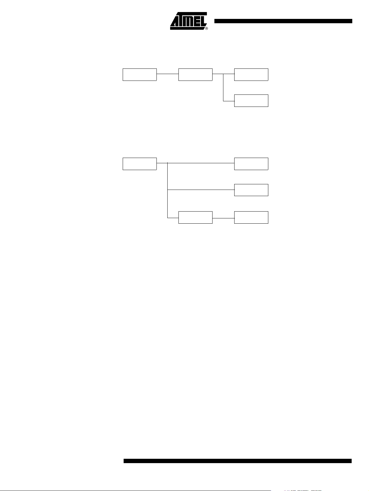
AT8xC5122/23
)
)
Figure 21. X1 mode
Crystal
8 MHz
PR1 prescaler
1/2
CPU frequency
4 MHz
Peripheral frequency
4 MHz
When the X1 mode is selected, the CPU and Peripherals work at 8Mhz / X1
Figure 22. X2 mode
Crystal
8 MHz
Internal Prescaler
1/2
CPU frequency (X2 Mode)
8 MHz
Peripheral frequency (X2 mode
8 MHz
Peripheral frequency (X1 mode
4 MHz
When the X2 mode is selected, the CPU works at 8 MHz / X2. The Peripherals can work
at 8 MHz / X2 or 8 MHz / X1.
When the PR1 prescaler is different from 1/2 , the usual X1 mode can not be defined. I n
this case, it is necessary to define a X1 or X2 equivalent mode from equivalent clock
circuits.
Example : PR1=1/8, X2=0.
In this configuration, the CPU works at 1 MHz. This frequency could also be obtained by
an equivalent cloc k circuit where t he on-chip o scillator woul d run at 2 MHz in X1 mod e
or at 1 MHz in X2 mode. So we can say that the CPU works at 2 MHz / X1 or 1MHz / X2.
As the X2 bit is cleared in CKCON0 register, we have F
CK_IDLE
= F
CK_PERIPH
.
46
4202E–SCR–06/06
Page 47
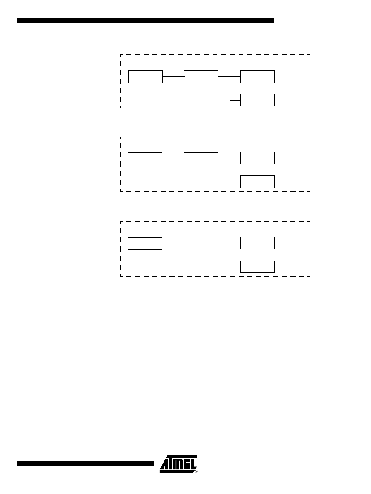
AT8xC5122/23
Crystal
8 MHz
External Clock
2 MHz
External Clock
1 MHz
PR1 Prescaler
1/8
(Equivalent to)
X1 mode selected
1/2
(Equivalent to)
X2 mode selected
CPU frequency
1 MHz
PERIPH frequency
1 MHz
CPU frequency
1 MHz
PERIPH frequency
1 MHz
CPU frequency
1 MHz
PERIPH frequency
1 MHz
Use of PLL Clock When the CPU clock is fed by the P LL, the X2 mode is forbi dden. The bit X2 m ust
always remain cleared in CKCON0 register. As the PR1 prescaler is always different
from 1/2, the usual X1 mode can not be defined. So it is neces sary to defi ne an eq uivalent X1 or X2 mode from equivalent clock circuits, as in previous section.
Examp le: P R1= 1/4 , PL L feed s th e C PU. T he C PU works in this ca se at 2 4 MH z. Thi s
frequency could also be ob tai ned by an equivalent clock circuit where th e on-c hip osc illator would run at 48 MHz in X1 mode o r at 24 Mhz in X2 mode. So we c an say that in
this configuration, the CPU works at 48 MHz / X1 or 24 MHz / X2 (See figures below).
As the X2 bit is cleared in CKCON0 register, we have always F
CK_IDLE
= F
CK_PERIPH
.
4202E–SCR–06/06
47
Page 48

AT8xC5122/23
PLL
96 MHz
External Clock CPU frequency
48 MHz
External Clock
24 MHz
Prescaler
1/4
(Equivalent to)
X1 mode selected
1/2
(Equivalent to)
X2 mode selected
CPU frequency
24 MHz
PERIPH frequency
24 MHz
24 MHz
PERIPH frequency
24 MHz
CPU frequency
24 MHz
PERIPH frequency
24 MHz
SCIB Clock The Smart Card Interface Block (SCIB) uses two clocks :
– The first one, CK_IDLE, is the peripheral clock used for the interface with the
microcontroller.
– The second one, CK_ISO, is independant from the CPU clock and is
generated from the PLL or XTAL1 output.
PR2, a 6-bit prescaler, will be used to generate:
12/9.6/8/6.85/6/5.33/4.8/4.36/ ..../1MHz frequencies.
SCIB clock frequency must be lower than CPU clock frequency.
During SCIB Reset, the CK_ISO input m ust be in the range 1 - 5 M H z ac cording to ISO
7816. The SCIB clocks frequency is defined in Figure 42 on page 74 and Tab le 42 on
page 74.
Two conditions must be met for a correct use of the SCIB:
• CK_CPU > 4/3 * CK_ISO and
• CK_CPU < 6 * CK_ISO.
48
4202E–SCR–06/06
Page 49

AT8xC5122/23
If the CK_CPU <= 4/3 * CK_ISO, the SCIB doesn’t work.
If the CK_CPU >= 6* CK_ISO, the programmer must take care in three cases:
• Read (or write) operation on a SCIB register followed immediatly with an other Read
(or write) operation on the same register.
• Read (or write) operation on a SCIB register followed immediatly with an other Read
(or write) operation on a linked register. The list of linked registers is in the table
below.
Linked registers
Write in SCICR and after read of SCETU0-1
Write in SCIBUF and after read of SCISR
• Write operation on a register of the list below followed immediatly with a read
operation on a SCIB register.
Wait after Write operation on thi s registers
SCICR, SCIER, SCETU0-1,SCGT0-1,
SCWT0-3,SCCON
To avoid any trouble, a delay must be added between the two accesses on the SCIB
register. The SCIB must complete the first read (or write) operation before to receive the
second. A solution is to add NOP (no operation) instructions. The number of NOP to add
depends of the rate between CK_CPU and CK_ISO (see table below).
Number of
Min CLK_CPU Max CLK_CPU
CLK_CPU >= 6 * CLK_ISO CLK_CPU <= 12 * CLK_ISO 6 ( example1 NOP)
CLK_CPU >= 12* CLK_ISO CLK_CPU <= 16 * CLK_ISO 12 ( example 2 NOP)
CPU cycles to add
Alternate Card Clock The alternate Card uses the peripheral clock divided by the PR3 prescaler. (1; 1/2; 1/4;
1/8 divisi on ratio ). See Section "A lterna te Ca rd", pa ge 78 for the de finit ion of the alte rnate clock.
DC/DC Converter Clock The DC/DC block needs a clock with a 50% duty cycle. The frequency must also be
included in the range 3. 68 M Hz an d 6 M H z. The P R4 presc aler is used t o configure the
DC/DC frequency.
XTAL1 (MHz) DCCKPS3:0 value Prescaler Factor DC/DC converter CLK (MHz)
4202E–SCR–06/06
802 4
49
Page 50

AT8xC5122/23
USB Interface Clock The USB Interface uses two clocks :
– The first one is the CPU clock used for the interface with the microcontroller,
CK_IDLE.
– The second one is the CK_USB supplied from the PLL through a divider by
2.
Registers
Table 24. Clock Selection Register - CKSEL (S:85h)
76543210
-------CKS
Bit Number Bit Mnemonic Description
7:1 -
0CKS
Reserved
The value read from this bit is indeterminate. Do not set this bit.
CPU Oscillator Select Bit
Set this bit to connect CPU and Peripherals to PLL output.
Clear this to to connect CPU and Peripherals to XTAL1 clock input.
Reset Value = XXXX XXX0b
Table 25. Clock Reload Register - CKRL (S:97h)
76543210
- - - - CKRL 3 CKRL2 CKRL1 CKRL0
Bit Number Bit Mnemonic Description
7 - 4 -
3:0 CKRL3:0
Reserved
The value read from this bit is indeterminate. Do not set this bit.
Clock Reload register
Prescaler1 va lu e
=[ 1 / 2*( 16-CKRL)] * F
F
ck_cpu
ck_XTAL1
Reset Value = XXXX 1111b
50
4202E–SCR–06/06
Page 51

AT8xC5122/23
Table 26. Clock Configuration Register 0 - CKCON0 (S:8Fh)
76543210
-WDX2- SIX2 - T1X2T0X2X2
Bit Number Bit Mnemonic Description
7-
6WDX2
5-
4SIX2
3-
2T1X2
1T0X2
0X2
Reset Value = X0X0 X000b
Reserved
The value read from this bit is indeterminate. Do not set this bit.
Watchdog clock
This control bit is validated when the CPU clock X2 is set; when X2 is low,
this bit has no effec t.
Cleare d to bypass the PR1 prescaler.
Set to select the PR 1 output for this periphe ral.
Reserved
The value read from this bit is indeterminate. Do not set this bit.
Enhanced UART clock (Mode 0 and 2)
This control bit is validated when the CPU clock X2 is set; when X2 is low,
this bit has no effec t.
Cleare d to bypass the PR1 prescaler.
Set to select the PR 1 output for this periphe ral.
Reserved
The value read from this bit is indeterminate. Do not set this bit.
Timer 1 clock
This control bit is validated when the CPU clock X2 is set; when X2 is low,
this bit has no effec t.
Cleare d to bypass the PR1 prescaler.
Set to select the PR 1 output for this periphe ral.
Timer 0 clock
This control bit is validated when the CPU clock X2 is set; when X2 is low,
this bit has no effec t.
Cleare d to bypass the PR1 prescaler.
Set to select the PR 1 output for this periphe ral.
System clock Control bit
Cleared to select the PR1 output for CPU and all the peripherals .
Set to byp a ss the PR1 p r esc aler an d to en ab le th e indi vi du al pe rip hera ls ‘X 2’
bits.
4202E–SCR–06/06
51
Page 52

AT8xC5122/23
Table 27. Clock Configuration Register 1 - CKCON1 (S:AFh) only for AT8xC5122
76543210
-------SPIX2
Bit Number Bit Mnemonic Description
7 - 4 -
3-
0 SPIX2
Reserved
The value read from this bit is indeterminate. Do not set this bit.
Reserved
The value read from this bit is indeterminate. Do not set this bit.
SPI clock
This control bit is validated when the CPU clock X2 is set. When X2 is low,
this bit has no effec t.
Cleare d to bypass the PR1 prescaler.
Set to select the PR 1 output for this periphe ral.
Reset Value = XXXX XXX0b
Table 28. PLL Control Register - PLLCON (S:A3h)
76543210
- - - - - EXT48 PLLEN PLOCK
Bit Number Bit Mnemonic Description
7 - 3 -
2 EXT48
Reserved
The value read from these bits is always 0. Do not set this bits.
External 48 MHz Enable Bit
Set this bit to select XTAL1 as USB clock.
Clear this bit to select PLL as USB clock.
SCIB clock is controlled by EXT48 bit and XTSCS bit.
52
PLL Enable bit
1PLLEN
0PLOCK
Set to enable the PLL.
Clear to disable the PLL.
PLL Lock Indicator
Set by hardware when PLL is locked
Clear by hardware when PLL is unlocked
Reset Value = 0000 0000b
Table 29. PLL Divider Register - PLLDIV (S:A4h)
76543210
R3 R2 R1 R0 N3 N2 N1 N0
Bit Number Bit Mnemonic Description
7 - 4 R3:0 PLL R Divider Bits
3 - 0 N3:0 PLL N Divider Bits
Reset Value = 0000 0000b
4202E–SCR–06/06
Page 53

I/O Port Definition
Ports vs Packages Table 30. I/O Number vs Packages
P0 P1 P2 P3 P4 P5 Tot al
AT8xC5122/23
VQFP64
QFN64
VQFP32
QFN32
PLCC28-6-6-113
88886846
-8-8-117
Port 0 Port 0 has the following functions:
– Default function: Port 0 is an 8-bit I/O port.
– Alternate function: Port 0 is also the multiplexed low-order address and data
bus during accesses to external Program and Data Memory. In this
application, it uses strong internal pull-ups when emitting 1’s and it can drive
CMOS inputs without external pull-ups.
Port 0 has the following configurations:
– Default configuration: open drain bi-directional I/O port. Port 0 pins that have
1’s written to them float, and in this state they can be used as high-
impedance inputs.
– Configuration 2: Low speed output, “KB_OUT”
– Configuration 3: Push-pull output
4202E–SCR–06/06
53
Page 54

AT8xC5122/23
Port 1 Port 1 has the following functions:
– Default function : Only Port 1.2, P1.6 and P1.7 are standard I/O’s; the other
ports can be activated only with the SCIB function.
– Alternate function and configu ration: see Table 31.
Table 31. Port 1 Description.
Alternate Function Configuration
Port
P1.2 CPRES
P1.6 SS
P1.7 CCLK1 Alternate Card Clock output
Signal Description Mode Comments
CIO
CC8
CC4
CCLK
CRST
Smart card interface function
Card I/O
Smart card interface function
Card contact 8
Smart card interface function
Card presence
Smart card interface function
Card contact 4
Smart card interface function
Card clock
Smart card interface function
Card reset
SS pin of the SPI function Quasi-bidirectional supplied by VCC
Quasi- bidirect ional port supplied by
DC/DC converter
Quasi- bidirect ional port supplied by
DC/DC converter
Quasi- bidirect ional port supplied by VCC
Quasi- bidirect ional port supplied by
DC/DC converter
Push-Pull port supplied by DC/DC
converter
Push-Pull port supplied by DC/DC
converter
Quasi- bidirectional supplied by VCC Alternate Ca rd Clock function disabled
Quasi-bidirectional supplied by VCC
Low level at reset.
Caution : if DPU bit is set in AUXR register, the
weak-pull of the port is disabled
Low level at reset
Caution : if DPU bit is set in AUXR register, the
weak-pull of the port is disabled
Weak & medium pull-up’s can be disconnected
by CPRESRES bit in PMOD0 regsiter
High Level at reset
Low level at reset
Caution : if DPU bit is set in AUXR register, the
weak-pull of the port is disabled
Low level at reset
Low level at reset
Altern at e S m art C ard Clock enab led
Switched automatically to Push-pu ll (see Table
47 on page 82 )
Port 2 Port 2 has the following functions:
– Default function: Port 2 is an 8-bit I/O port.
– Alternate function 1: Port 2 is also the multiplexed high-order address during
accesses to external Program and Data Memory. In this application, it uses
strong internal pull-ups when emitting 1’s and it can drive CMOS inputs
without external pull-ups.
Port 2 has the following configurations:
– Default configuration: Pseudo bi-directional “Port51” digital input/output with
internal pull-ups.
– Configuration 1: Push-pull output
– Configuration 2: Low speed output, “KB_OUT
– Configuration 3: Input with weak pull-up, “WPU input”
54
4202E–SCR–06/06
Page 55

Port 3 Port 3 has the following functions:
– Default function: Port 3 is an 8-bit I/O port.
– Alternate functions : see table below
Port 3 has the following configurations:
– Default configuration: Pseudo bi-directional “Port51” digital input/output with
internal pull-ups.
– Alternate configurations: See Table 32.
Table 32. Port 3 Description
Alternate Functions Configurations
AT8xC5122/23
Port
P3.0 RxD
P3.1 TxD
P3.2 INT0 External interrupt 0 input/timer 0 gate control input LED0
P3.3 INT1 External interrupt 1input/timer 1 gate control input Push-pull KB_OUT Input WPU
P3.4 T0 Timer 0 coun ter inpu t Push-pull KB_OUT Input WPU LED1
P3.5 T1 Timer 1 coun ter input
P3.6 WR
P3.7 RD
Signal Descripti on Mode 1 Mode 2 Mod e 3 Mode 4
Receiver data input (asynchronous) or data input/output
(synchronous) of the serial interface
Transmitter data output (asynchronous) or clock output
(synchronous) of the serial interface
External Data Memory write strobe; latches the data byte
from port 0 into the external data memory
External Data Memory read strobe; Enables the external
data memor y. Port 3 can drive C MOS in pu t s wit ho ut ext e rna l
pull-ups
Push-p ull KB_OUT Input WP U
Push-p ull KB_OUT Input WP U
LED2
LED3
4202E–SCR–06/06
55
Page 56

AT8xC5122/23
Port 4 Port 4 has the following functions:
– Default function: Port 4 is an 6-bit I/O port.
– Alternate functions : see table below
Port 4 has the following configurations:
– Default configuration: Pseudo bi-directional “Port51” digital input/output with
internal pull-ups.
– Alternate configurations: See Table 33.
Table 33. Port 4 Description
Alternate Functions Configurations
Port
P4.0 MISO SPI Master In Slave Out I/O
P4.1 MOSI SPI Master Out Slave In I/O
P4.2 SCK SPI clock
P4.3 Push-pull KB_OUT Input MPU
P4.4 Push-pull KB_OUT Input MPU
P4.5 Push-pull KB_OUT Input MPU
Signal Description Mode 1 Mode 2 Mode 3
Port 5 Port 5 has the following functions:
– Default function: Port 5 is an 8-bit I/O port.
– Alternate function 1: Port 5 is an 8-bit keyboard port KB0 to KB7.
Port 5 has the following configurations:
– Default configuration: Pseudo bi-directional “Port51” digital input/output with
internal pull-ups.
– Alternate configuration: see T able 34.
Table 34. Port 5 Description
Configurations
56
Port
P5.0 Push-pull Input MPU Input WPU
P5.2 Push-pull Input MPU Input WPU
P5.3 Push-pull Input WPD Input WPU
P5.4 Push-pull Input WPD Input WPU
P5.5 Push-pull Input WPD Input WPU
P5.6 Push-pull Input WPD Input WPU
P5.7 Push-pull Input WPD Input WPU
Mode 1 Mode 2 Mode 3 Comments
First clusterP5.1 Push-pull Input MPU Input WPU
Second cluster
Third cluster
4202E–SCR–06/06
Page 57

Port Configuration
Standard I/O P0 The P0 port is described in Figure 23.
Figure 23. Standard Input/Output Port
AT8xC5122/23
PMOS
NMOS
Vcc
Pin
ADDR/DATA
CONTROL
1
Port latch
Data
0
MUX
Vss
Input
Data
Quasi Bi-directional Port The default port output configuration for standard I/O ports is the quasi-bi-directional
output that is common on the 80C51 and most of its derivatives. The “Port51” output
type can be used as bot h an inpu t and ou tput witho ut the nee d to recon figure th e port.
This is possible because when the port outputs a logic high, it is weakly driven, allowing
an external device to pull the pin low.
When the port outputs a logic low state, it is driven strongly and is able to sink a fairly
large current.
These features are somewhat similar to an open-drain output except that there are three
pull-up transistors in the quasi-bi-directional output that serve different purposes.
One of these pull-ups, called the wea k pull-up, is turne d on whenever t he port latch for
the pin contains a logic 1. The weak pull-up sources a very small current that will pull the
pin high if it is left floatin g. The weak pull-up ca n be turned of f by the DPU b it in AUXR
register.
A second pull-up, called the medium pull-up, is turned on when t he port latch for the pin
contains a logic 1 and the pin itself is also at a logic 1 level. This pull-up provides the primary source current for a quasi-bi-directional pin that is outputting a 1. If a pin that has a
logic 1 on it is pulled low by an external device, the medium pull-up turns off, and only
the weak pull-up remains on. In order to pull the pin low under these conditions, the
external dev ice h as to sink e no ugh cu rre nt to o ver power the medi um pull-up an d ta ke
the voltage on the port pin below its input threshold.
Note: for CIO, CC4, CC8 ports of SCIB interface , in input mode when the ICC (smart card) is
driving the port pin :
– if 0 < Vin < CVCC/2 : weak pull-up is active (~100KOhm)
– if CVCC/2 < Vin < CVCC : weak (~100KOhm) and medium (~12KOhm) pull-
up’s are active
4202E–SCR–06/06
57
Page 58
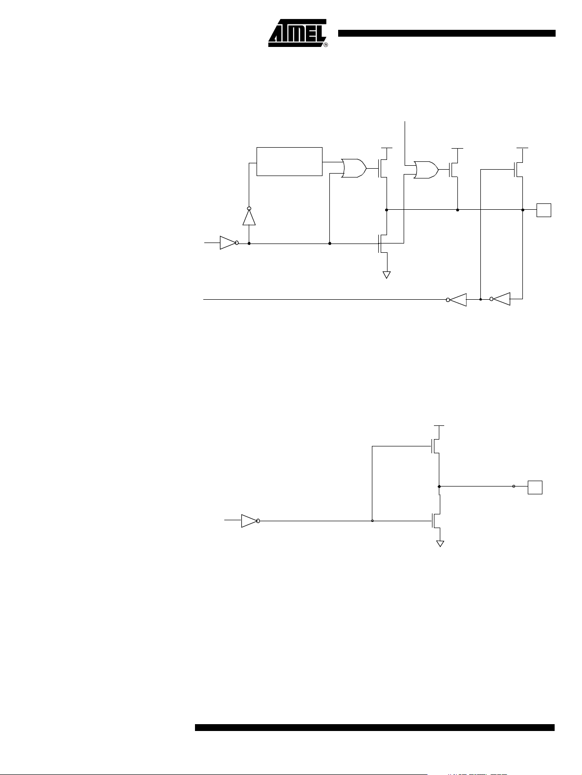
AT8xC5122/23
n
The “Port51” is described in Figure 24.
Figure 24. Quasi Bi-directional Port
2 CPU
CLOCK DELAY
DPU (AUXR.7)
vcc vcc vcc
P
Strong Weak Medium
P
P
Push-pull Out p ut Configuration
Port Latch
Data
Input
Data
N
Vss
Pi
The push-pull output configuration has the same pull-down structure as both the open
drain and the quas i-bi- direct ional out put mod es, bu t provid es a co ntinuou s stro ng pul lup when the port latc h cont ains a logic 1. The push-pull mode m ay be used when more
source current is needed from a port output.
The Push-pull port configuration is shown in Figure 25.
Figure 25. Push-pull Output
P
PMOS
Port latch
Data
Strong
Pin
N
NMOS
Input with Medium or Weak Pull-up Configuration
58
The input with pull-up (Input MPU and Input WPU) configuration is shown in Figure 26.
4202E–SCR–06/06
Page 59

Figure 26. Input with Pull-up
AT8xC5122/23
Input with Weak Pull-down Configuration
Low Speed Output Configuration
Stuck to 0 if Medium
Stuck to 0 if Weak
Input
Data
P
P
Medium
Weak
Pin
The input with pull-down (input WPD) configuration is shown in Figure 27
Figure 27. Input with Pull-down
Input
Data
Pin
Weak
The low speed output with low speed t
FALL
and t
1
can drive keyboard.
RISE
N
The current limitation of the LED2CTRL block requires a polarisation current of about
250 µA. This block is automatically disabled in power-down mode.
The low speed output configuration (KB_OUT) is shown in Figure 28.
Figure 28. Low-speed Output
Port latch
Data
PCON.1
LED Sourc e Cu rrent The LED configuration is shown in Figure 29.
PWEAKCTRL
NMOS
LED2CTRL
P
Weak
Pin
N
N
4202E–SCR–06/06
59
Page 60
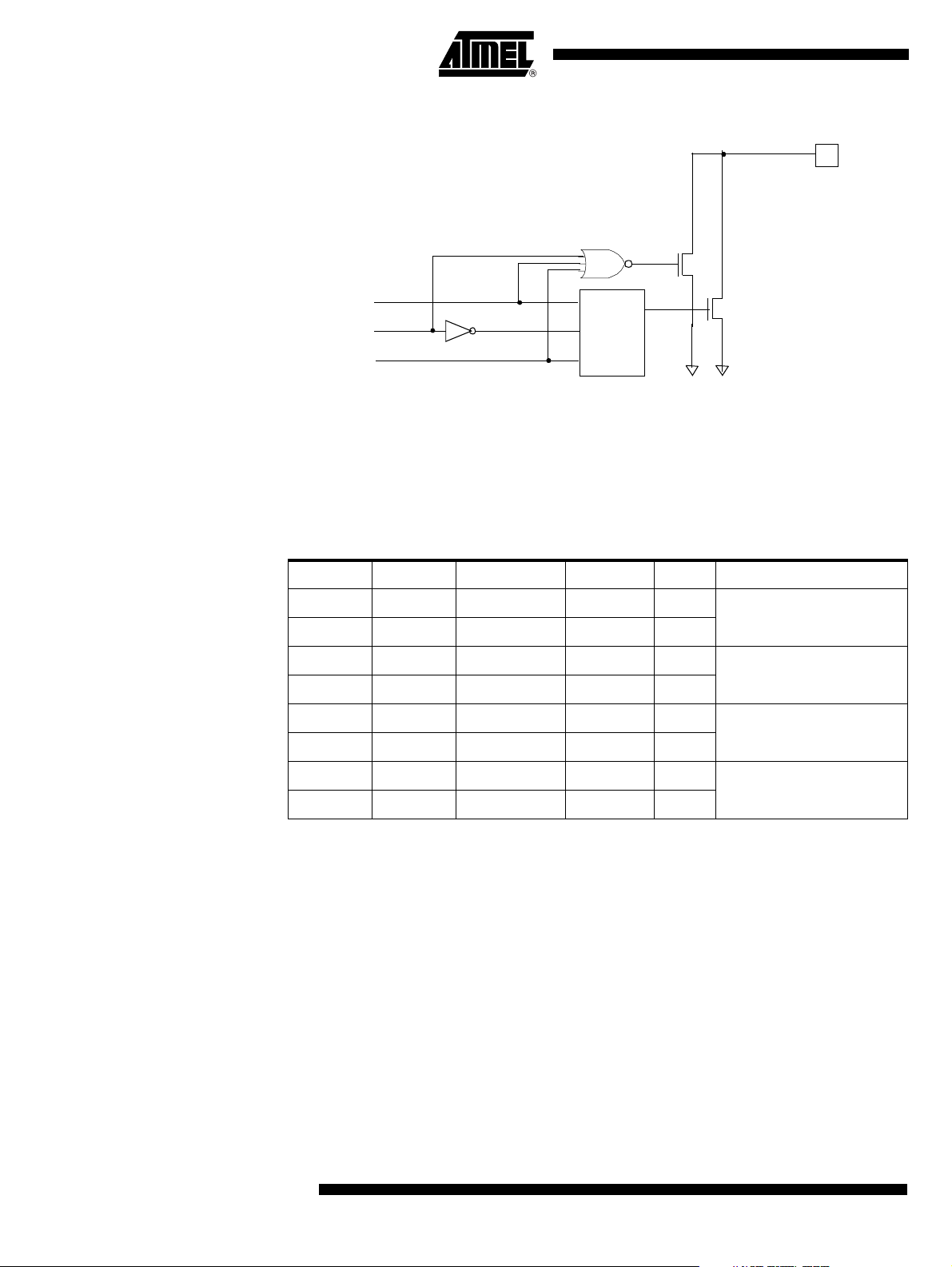
AT8xC5122/23
Figure 29. LED Source Current
Pin
NMOS
LEDx.0
Port Latch
Data
LEDx.1
Notes: 1. When switching a low level, LEDCTRL device has a permanent current of about
N mA/15 (N is 2, 4 or 8).
2. The port must be configured as standard C51 port by means of PMOD0 and PMOD1
registers and the level of current must be programmed by means of LEDCON0 and
LEDCON1 registers before switching the led on.
LEDCTRL
N
N
Table 35. LED Source Current
LEDx.1 LEDx.0 Port Latch Data NMOS PIN Comments
00 0 10
00 1 01
01 0 00
01 1 01
LED co ntrol disabl ed
LED mode 2 mA
10 0 00
10 1 01
11 0 00
11 1 01
LED mode 4 mA
LED mode 10 mA
60
4202E–SCR–06/06
Page 61

Registers
AT8xC5122/23
Table 36. Port Mode Register 0 - PMOD0 (91h) for AT8xC5122
7654 3 210
P3C1 P3C0 P2C1 P2 C0 CPRESRES - P0C1 P0C0
Bit Number Bit Mnemonic Description
Port 3 Configuration bits (Applicable to P3.0, P3.1, P3.3, P3.4 only)
00 Quasi bi-directional
7 - 6 P3C1-P 3C 0
5-4 P2C1-P2C0
3 CPRESRES
01 Push-pull
10 Output Low Spe ed
11 Input with weak pull-up
Port 2 Configuration bits
00 Quasi bi-directional
01 Push-pull
10 Output Low Spe ed
11 Input with weak pull-down
Card Presence Pull-up resistor
Cleared to connect the internal 100K pull-up
Set to disconnect the internal pull-up
2-
1-0 P0C1-P0C0
Reserved
The value read from this bit is indeterminate. Do not set this bit.
Port 0 Configuration bits
00 C51 Standard P0
01 Reserved
10 Output Low Spe ed
11 Push-pull
Reset Value = 0000 0x00b
Table 37. Port Mode Register 0 - PMOD0 (91h) for AT83C5123
7654 3 210
P3C1 P3C0 - - CPRESRES - - -
Bit Number Bit Mnemonic Description
Port 3 Configuration bits (Applicable to P3.0, P3.1, P3.3, P3.4 only)
00 Quasi bi-directional
7 - 6 P3C1-P 3C 0
5-4
3 CPRESRES
01 Push-pull
10 Output Low Spe ed
11 Input with weak pull-up
Reserved
The value read from these bits are indeterminate. Do not set these bit.
Card Presence Pull-up resistor
Cleared to connect the internal 100K pull-up
Set to disconnect the internal pull-up
4202E–SCR–06/06
2-0 -
Reset Value = 00xx 0xxxb
Reserved
The value read from these bits are indeterminate. Do not set these bit.
61
Page 62

AT8xC5122/23
Table 38. Port Mode Register 1 - PMOD1 (84h) for AT8xC5122
76543210
P5HC1 P5HC0 P5MC1 P5MC0 P5LC1 P5LC0 P4C1 P4C0
Bit Number Bit Mnemonic Description
Port 5 High Configuration bits (Applicable from P5.6 to P5.7 only)
00 Quasi bi- directi onal
7 - 6 P5HC1-P5HC0
5 - 4 P5MC1-P5MC0
3 - 2 P5LC1-P5 LC0
01 Push-pull
10 Input with weak pull-down
11 Input with weak pull-up
Port 5 Medium Configuration bits (Applicable from P5.3 to P5.5 only)
00 Quasi bi- directi onal
01 Push-pull
10 Input with weak pull-down
11 Input with weak pull-up
Port 5 Low Configuration bits (Applicable from P5.0 to P5.2 only)
00 Quasi bi- directi onal
01 Push-pull
10 Input with medium pull-up
11 Input with weak pull-up
Port 4 Configuration bits (Applicable from P4.3 to P4.5 only)
00 Quasi bi- directi onal
1 - 0 P4C1-P 4 C 0
01 Push-pull
10 Output Low Spe ed
11 Input with medium pull-up
Reset Value = 0000 0000b
Table 39. Port Mode Register 1 - PMOD1 (84h) for AT83C5123
76543210
----P5LC1P5LC0--
Bit Number Bit Mnemonic Description
7 - 4
3 - 2 P5LC1-P5 LC0
1 - 0
Reserved
The value read from this bit is indeterminate. Do not set this bit.
Port 5 Low Configuration bits (Applicable from P5.0 to P5.2 only)
00 Quasi bi- directi onal
01 Push-pull
10 Input with medium pull-up
11 Input with weak pull-up
Reserved
The value read from this bit is indeterminate. Do not set this bit.
Reset Value = xxxx 00xxb
62
4202E–SCR–06/06
Page 63

AT8xC5122/23
Table 40. LED Port Control Register 0 - LEDCON0 (F1h)
76543210
LED3.1 LED3.0 LED2.1 L ED2 .0 LED1.1 LED1 .0 LED0.1 LED0.0
Bit Number Bit Mnemonic Description
Port LED3 Config urat ion bit s
7 - 6 LED 3
5 - 4 LED 2
3 - 2 LED 1
00 LED control disabled
01 2 mA current source when P3.7 is configured as Quasi-bi-directional mode
10 4 mA current source when P3.7 is configured as Quasi-bi-directional mode
11 10 mA current source when P3.7 is configured as Quasi-bidir ect. mode
Port LED2 Config urat ion bit s
00 LED control disabled
01 2 mA current source when P3.6 is configured as Quasi-bi-directional mode
10 4 mA current source when P3.6 is configured as Quasi-bi-directional mode
11 10 mA current source when P3.6 is configured as Quasi-bidir ect. mode
Port LED1 Config urat ion bit s
00 LED control disabled
01 2 mA current source when P3.4 is configured as Quasi-bi-directional mode
10 4 mA current source when P3.4 is configured as Quasi-bi-directional mode
11 10 mA current source when P3.4 is configured as Quasi-bidir ect. mode
Port LED0 Config urat ion bit s
1 - 0 LED 0
00 LED control disabled
01 2 mA current source when P3.2 is configured as Quasi-bi-directional mode
10 4 mA current source when P3.2 is configured as Quasi-bi-directional mode
11 10 mA current source when P3.2 is configured as Quasi-bidir ect. mode
Reset Value = 0000 0000b
Table 41. LED Port Control Register 1- LEDCON1 (F1h) only for AT8xC5122
76543210
- - LED6.1 LED6.0 LED5.1 LED5.0 LED4.1 LED4.0
Bit Number Bit Mnemonic Description
7 - 6
5 - 4 LED 6
3 - 2 LED 5
Reserved
The value read from this bit is indeterminate. Do not set this bit.
Port LED6 Config urat ion bit s
00 LED control disabled
01 2 mA current source when P4.5 is configured as Quasi-bi-directional mode
10 4 mA current source when P4.5 is configured as Quasi-bi-directional mode
11 10 mA current source when P4.5 is configured as Quasi-bidir ect. mode
Port LED5 Config urat ion bit s
00 LED control disabled
01 2 mA current source when P4.4 is configured as Quasi-bi-directional mode
10 4 mA current source when P4.4 is configured as Quasi-bi-directional mode
11 10 mA current source when P4.4 is configured as Quasi-bidir ect. mode
4202E–SCR–06/06
Port LED0 Config urat ion bit s
1 - 0 LED 4
00 LED control disabled
01 2 mA current source when P4.3 is configured as Quasi-bi-directional mode
10 4 mA current source when P4.3 is configured as Quasi-bi-directional mode
11 10 mA current source when P4.3 is configured as Quasi-bidir ect. mode
Reset Value = 0000 0000b
63
Page 64

AT8xC5122/23
Smart Card Interface Block (SCIB)
The SCIB provides all signals to interface directly with a smart card. The compliance
with the ISO7816, EMV’2000, GSM and WHQL standards has been ce rtified.
Both synchronous (e.g. memory card) and asynchronous smart cards (e.g. microprocessor card) are supported. The component supplies the different voltages requested by
the smart card. The power off sequence is directly managed by the SCIB.
The card presence switch of the smart card connector is used to detect card insertion or
card removal. In case of card removal, the SCIB de-activates the smart card using the
de-activation sequence. An interrupt can be generated when a card is inserted or
removed.
Any malfunction is reported to the microcontroller (interrupt + control register).
The different operating modes are configured by internal registers.
• Support of ISO/IEC 7816
• character mode
• one transmit/receive buffer
• 1 1 bits ETU counter
• 9 bits guard time counter
• 32 bits waiting time counter
• Auto character repetition on error signal detection in transmit mode
• Auto error signal generation on parity error detection in receive mode
• Power on and power off sequence generation
• Manual mode to drive directly the card I/O
64
4202E–SCR–06/06
Page 65
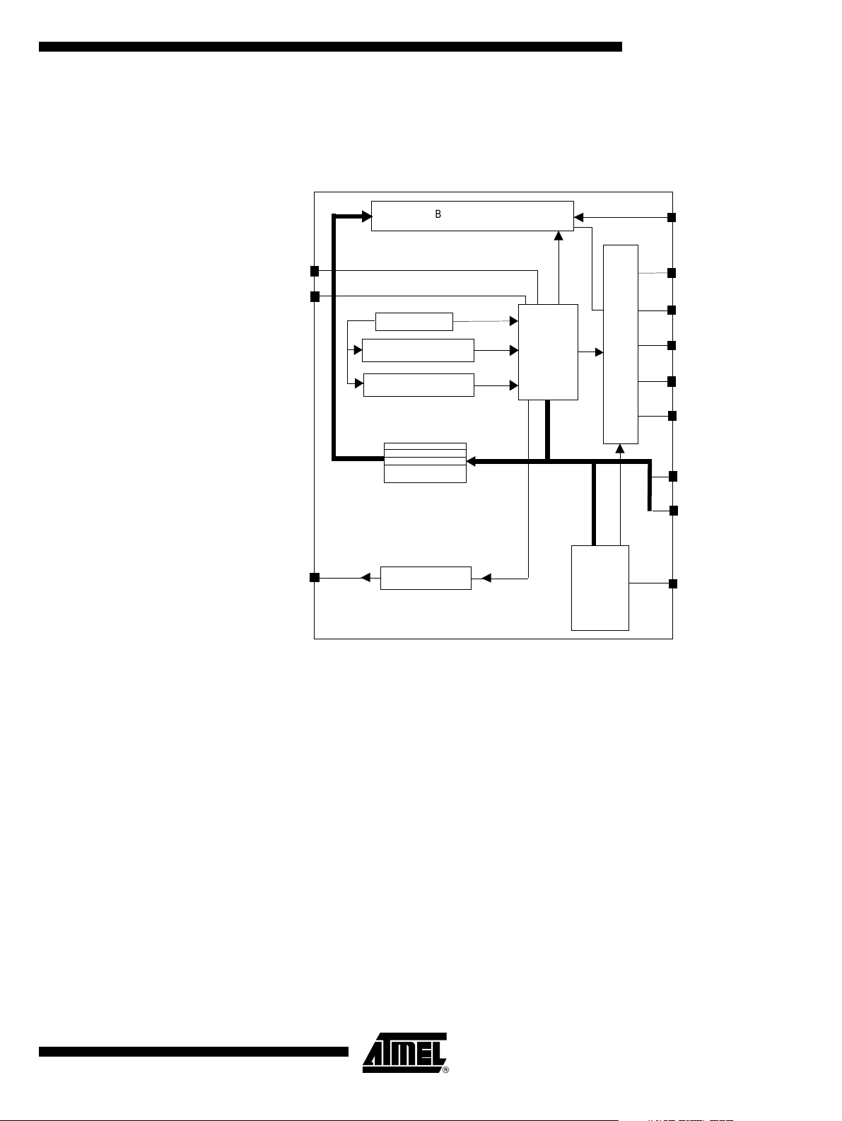
Block Diagram
The Smart Card Interface Block diagram is shown Figure 30:
Figure 30. SCIB Block Diagram
Ba rr el sh ifte r
AT8xC5122/23
IO (in)
Clk_iso
Clk_cpu
INT
Etu counter
Guard time counter
Waiting time counter
SCI Registers
Interrupt generator
Scart
fsm
I/O
mux
Power on
Power off
fsm
IO (out)
CLK
RST
C4 (o ut)
C8 (out)
C4 (in)
C8 (in)
VCARD
Definitions This paragraph introdu ces some of the terms used in ISO 7816-3 and E MV recom m en-
dations. Please refer to the full recommendations for a complete list of terms.
Terminal and ICC Terminal is the reader, ICC is the Integrated Circuit Card ETU Elementary Timing Unit (Bit time) T=0 Character oriented half duplex protocol T=0 T=1 Block oriented half duplex protocol T=1 Activation: Cold Reset Re set initiated by the Term inal with Vcc power-up. Th e card will answer with ATR (see
below)
Activation: Warm Reset Reset initiated by the Terminal with Vcc already powered-up, and after a prior ATR or
Warm Reset
De-Activation Deactivation by the Terminal as a result of : unresponsive ICC, or ICC removal.
4202E–SCR–06/06
65
Page 66

AT8xC5122/23
ATR Answer To Reset. Response from the ICC to a Reset initiated by the Terminal F and D F = Clock Rate Conv ersi on F acto r, D = B it rate ad justm ent fa ctor . ETU is de fined as :
ETU = F/(D*f) with f = Card Clock frequency . If f is in Hertz, ETU is in second. F and D
are available in the ATR (byte TA1). The default values are F=372, D=1.
Guard Time The ti me betwee n 2 lea din g edg es of th e sta rt b it o f 2 c onsec uti ve chara ct ers is com-
prised of the character duration (10) plus the guard time. Be aware that the Guard Time
counter and the Guard Time registers in the AT8xC5122/23 consider the time between 2
consecutive charac ters. So the equation is Guard Time C ounter = Guard Time + 10. In
other w or ds, the G ua rd Ti me is the n umb er of S t op Bi ts b etw een 2 ch ar acte rs s ent i n
the same direction.
Extra Guard Time ISO IEC 7816-3 and EMV introduc e th e Extra Gua rd time t o be adde d to the m inimum
Guard Time . Extra Gu ard Time onl y apply to con secutive ch aracters sent by the t erminal to the ICC. The T C1 byte in the A TR def ine the num ber N. For N=0 the character to
character duration is 12 ETUs. For N=254 the character to character duration is 266. For
N=255 (special case) The minimum character to character duration is to be used : 12 for
T=0 protocol and 11 for T=1 protocol.
Block Guard Time The time betwee n the le ading ed ges of 2 co nsecutive charact ers se nt in opposi t direc-
tion. ISO IEC 7816-3 and EMV recommend a fixed Block Guard Time of 22 ETUs.
Work Waiting Time (WWT) In T=0 protocol WWT is the interval between the leading edge of any character sent by
the ICC, and the leading edge of the previous character sent either by the ICC or the
Terminal. If no char acter is received b y the t erminal after W WTm ax time, t he Te rminal
initiates a De-Activation Sequence.
Character Waiting Time (CWT) In T=1 protocol CWT is the interval between the leading edge of 2 consecut ive charac-
ters sent by the ICC. If the next character is not received by the Terminal after CWTmax
time, the Terminal initiates a De-Activation Sequence.
Block Waiting Time (BWT) In T=1 pro tocol BWT is the interval between the l eading ed ge of the start bi t of the last
character sent by the Terminal that gives the right to sent to the ICC, and the leading
edge of the start bit of the first character sent by the ICC. If the first character from the
ICC is not received by the Terminal after BWTmax time, the Terminal initiates a De-Activation Sequence.
Waiting Time Extention (WTX) I n T= 1 prot ocol the ICC can reques t a Wa iting T im e Exten sio n with a S(W TX re quest )
request. The Terminal should acknowlege it. The Waiting time between the leading
edge of the start bit of the last character sent by the Terminal that gives the right to sent
to the ICC, and the leading edge of the start bit of the first character sent by the ICC will
be BWT*WTX ETUs.
Parity error in T=0 protocol In T=0 protocol, a Terminal (respectively an ICC) detecting a parity error while receiving
a character shall force the Card IO line at 0 starting at 10.5 ETUs, thus reducing the first
Guard bi t by ha lf the t ime. Th e Ter minal (res pect ivel y an IC C) sh all mai ntain a 0 f or 1
ETU min and 2 ETUs max (according to ISO IEC) or to 2 ETUs (according to EMV). The
ICC (respectively a Terminal) shall monitor the Card IO to detect this error signal then
attempt to repeat the character. According to EMV, following a parity error the character
can be repeated one time, if parity error is detected again this procedure can be
repeated 3 more times. The same character can be transmitted 5 times in total. ISO
66
4202E–SCR–06/06
Page 67

AT8xC5122/23
IEC7816-3 says this procedure is mandatory in ATR for card supporting T=0 while EMV
says this procedure is mandatory for T=0 but does not apply for ATR.
Functional Description T he arch itecture of the Smart Card Interface Block can be detailed as follows:
Barrel Shifter The Barrel Shifter pe rforms t he tr anslati on bet ween 1 bit se rial dat a and 8 b its pa rallel
data
The barrel function is useful for character repetition since the character is still present in
the shifter at the end of the character transmission.
This shifter is able to shift the data in both directions and to invert the input or output
value in order to manage both direct and inverse ISO7816-3 convention.
Coupled with the barrel shifter is a parity checker and generator.
There are 2 regist ers conn ected to this barre l shifter, one for the trans mission and on e
for the reception. They act as buffers to relieve the CPU of timing constraints.
SCART FSM (Smart Card Asynchronous Receiver Transmitter Finite State Machine)
This is the core of the block. Its purpose is to control the barrel shifter. To sequence correctly the barrel shifter for a reception or a transmission, it uses the signals issued by the
different counters. One of the most important counters is the guard time counter that
gives time slots corresponding to the character frame.
The SCART FSM is enabled only in UART mode.
The transition from the receipt mode to the transmit mode is done automatically. Priority
is given to the transm ission. Transmissi on refers to Te rminal tran smission to th e ICC.
Reception refers to reception by the Terminal from the ICC.
ETU Counter The ETU (Elementary Timing Unit) counter controls the working frequency of the barrel
shifter, in fact it generates the enable signal of the barrel shifter. It receives the Card
Clock, and generat es t he ETU c l ock. T he Card Clock frequency is called “f ” below. The
ETU counter is 11 bit wide.
A special compensation mode can be activated. It accomodates situations where the
ETU is not an integer number of Card Clock (CK_ISO). The compensation mode is controlled by the COMP bit in SCETU1 register bit position 7. With COMP=1 the ETU of
every c hara cter even b its i s redu ce d by 1 C ar d C lock pe riod . As a resu lt, th e av erag e
ETU is : ETU_average = (ETU - 0.5). One should bear in mind that the ETU counter
should be programmed to deliver a faster ETU which will be reduced by the COMP
mechanism, not the other way around. This allows to reach the required precision of the
character duration specified by the ISO7816-3 standard.
Example1 : F=372, D=32 => ETU= F/D = 11.625 clock cycles.
We select ETU[10-0] = 12 , COMP=1. ETUaverage= 12 - (0.5*COMP) = 11.5
The result will be a full charac ter duration (10 bit) = (10 - 0. 107)* ETU. The EMV spec ifi-
cation is (10 +/- 0.2)*ETU
Guard Time C ounter The minimum time between the leading edge of the start bit of 2 consecutive characters
transmitted by the Terminal is controlled by the Guard Time counter, as described in
Figure 33.
4202E–SCR–06/06
67
Page 68
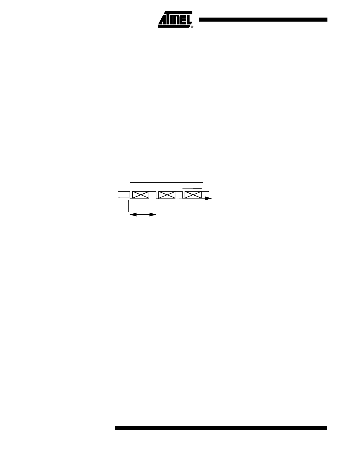
AT8xC5122/23
The Guard Time counter is an 9 bit counter It is initialized at 001h at the start of a transmission by the Terminal. It then increments itself at each ETU until it reach the 9 bit
value loaded into the SCGT1[0] concatenated with SCGT 0[7:0]. At this time a new Terminal transmission i s ena bled and the Guard Time Counter stop incrementing. As so on
as a new transmission start, the Guard Time Counter is re-initialized at 1 decimal value.
It should be noted that the value of the Guard Time Counter cannot be red. Reading
SCGT1,0 only gives the minimum time between 2 characters that the Guard Time
Counter will allow.
Care mus t be ta ken w i th th e G uard Tim e C o unter wh ich co unts the du rat ion betw ee n
the lead ing ed ges of 2 consec utive char acters. This correspo nd to the ch arac ter duration (10 ETU) pl us the Gu ard Time as d efine d by the IS O and EM V recom menda tions.
To program Guard Time = 2 : 2 stop bits between 2 characters which is equivalent to the
minimum delay of 12 ETUs between the leading edges of 2 consecutive characters,
SCGT1[0],SCGT0[7:0] should be loaded with the value 12 decimal. See Figure 31
Figure 31. Guard Time.
TRANSMISSION to ICC
CHAR n+1 CHAR n+2 CHAR n+3
>= SCGT
Block Guard Tim e C o unt er The Block Guard Time counter provides a way to program a minimum time between the
leading edge of the start bit of a character received from the ICC and the leading edge of
the start bit of a character sent by the terminal. ISO IEC 7816-3 and EMV recommend a
fixed Blo ck Gu ard Ti me of 22 ETUs . The AT 8xC512 2/23 offer th e po ssibility to ex tend
this delay up to 512 ETUs.
The Block Guard Time is a 9 bit counter. When the Block Guard Time mode is enabled
(BGTEN=1 in SCSR registe r) The Block G uard Time count er is initialized at 000h at the
start of each character transmissions from the ICC. It then increments at each ETU until
it reach the 9 bit value loaded into shado w SCGT 1,0 registers, or until it is re-initialized
by the start of an new transmiss ion from the ICC. If the Blo ck Guard Tim e counter
reaches the 9 bit value loaded into shadow SCGT1,0 registers, a transmission by the
TERMINAL is enabled, and the Block Guard Time counter stop incrementing. The Block
Guard Time counter is re-initialized at the start of each TERMINAL transmission.
The SCGT1 S CGT 0 s hado w regi sters are loaded with the cont ent of GT[8-0] contained
in the registers SCGT1[0),SCGT0(7: 0] with the rising edge of the bit BGTEN in the
SCSR register. See Figure 33.
68
4202E–SCR–06/06
Page 69

Figure 32. Block Guard Time.
it
AT8xC5122/23
ETU Counter
Enable
transmit
RECEPTION from ICC
Write SCGT1,0 with
a value for Guard Time
CHAR 1
CHAR 2
CHAR n
>= Block Guard Time
Write “Block Guard Time” in SCGT1,0
and set BGTEN to transfer the value to the
shadow SCGT1,0 registers
CHAR n+1 CHAR n+2 CHAR n+3
Figure 33. Guard Time and Block Guard Time counters
Guard Time Counter
Block Guard Time Counter
9 bits
Comparator
9 bits
9 bits
Shadow SCGT1 ,Shadow SCGT0
>= SCGT
TRANSMISSI ON to IC C
9 bits
Comparator
Enable
transm
GT[8:0]
SCGT1
SCGT0
To illustrat e the use of Gu ard Time an d Block Guard Time, let us cons ider the
ISO/IEC7816-3 recommendation : Guard Time = 2 (minimum delay between 2 consecutive characters sent by the Terminal = 12 ETUs), and Block Guard Time = 22 ETUs.
After A smart Card Reset
– Write 00decimal in SCGT1, Write 21decimal in SCGT 0
– Set BGTEN in SCSR (BGTEN was 0 before as a result of the smart card
reset)
– Write 12decimal in SCGT0
Now the Guard Time and Block Guard Time are properly initialized. The TERMINAL will
insure a minimun 12 ETUs between 2 leading edges of 2 consecutive characters transmitted. The TERMINAL will also insure a minimum of 22 ETUs between the leading
edge of a character sent by the ICC, and the leading edge of a character sent by the
TERMINAL. There is no need to write SCGT1,0 again and again.
Waiting Time (W T) Counter The WT counter is a 32 bits down counter which can be loaded with the value contained
in the SCWT3, SCWT2, SCWT1, SCWT0 registers. Its main purpose is timeout signal
generation. It is 32 bits wide and is decremented at the ETU rate. see Figure 34.
4202E–SCR–06/06
69
Page 70

AT8xC5122/23
Figure 34. Waiting Time Counter
When the WT counter times out, an interrupt is generated and the SCIB function is
locked: reception and emission are disabled. It can be enabled by resetting the macro or
reloading the counter.
The Waiting Time Counter can be used in T=0 protocol for the Work Waiting Time. It can
be used in T=1 protocol for the Ch arac ter W aiting Tim e and for t he Block Wai ting Time.
See the detailed explanation below.
ETU Counter
WTEN
Write_SCWT2
UART
Start Bit
WT Counter
Load
Timeout
WT[31:0]
SCWT3
SCWT2
SCWT1
SCWT0
In the s o c all ed m anu el mo de, t he co unter is loa ded, if W TE N = 0, duri ng t he w ri te of
SCWT2 register. The counter is loaded with a 32 bit word built with SCWT3 SCWT2
SCWT1 SCWT0 registers (SCWT0 contain WT[7-0] byte. WTEN is located in the
SCICR register.
When WTEN=1 and in UART mode, the counter is re-loaded at the occurenc e of a start
bit. This mode will be detailed below in T=0 protocol and T=1 protocol.
In manual mode, the WTEN signal controls the start of the counter (rising edge) and the
stop of the counter (falling edge). After a timeout of the counter, a falling edge on
WTEN, a reload of SCWT 2 and a risin g edge of WT EN are neces sary to start aga in the
counter and to release the SCIB macro. The reload of SCWT2 transfers all SCWT0,
SCWT1, SCWT2 and SCWT3 registers to the WT counter.
In UART mode there is an aut oma tic load on the start bit detection. This automatic load
is very usef ul for cha nging o n-the -fly the timeou t valu e since the re i s a register t o hol d
the load value. This is the case for T=1 protocol.
70
In T=0 protocol the maximun interval between the start leading edge of any character
sent by the ICC and the start of the previous character sent by either the ICC or the Terminal is the maximum Work Waiting Time. The Work Waiting Time shall not exceed
960*D*WI E TUs with D and WI p arameters a re return ed by the field TA1 and TC2
respectively in the A nswer To R eset (A TR). This is the val ue the us er shall write in th e
SCWT0,1,2,3 register. This value will be reloaded in the Waiting Time counter every
start bit.
4202E–SCR–06/06
Page 71

AT8xC5122/23
Figure 35. T=0 mode
> GT
CHAR 1
< WT
In T=1 protocol : The maximum interval between the leading edge of the start bit of 2
consecutive characters sent by the ICC is called maximum Character Waiting Time. The
Character Waiting Time shall not exceed (2**CWI + 11) ETUs with 0 =< BWI =< 5. Consequently 12 ETUs =< CWT =< 43 ETUs.
T=1 protocol also specify the maximum Block Waiting Time. This is the time between
the leading edge of the last character sent by the Terminal giving the right to send to the
ICC, and the leading edge of the start bit of the first character sent by the IC C. The
Block Waiting Time shall not exceed (2**BWI*960 + 11) ETUs with 0 =< BWI =< 4. Consequently 971 ETUs =< BWT =< 15371 ETUs.
CHAR 2
In T=1 protocol it is possible to extend the Block Waiting Time with the Waiting Time
Extension (WTX). When selected the waiting time becomes BW T*WTX ETUs. Th e
Waiting Time counter is 32 bit wide to accomodate this feature.
It is possible to take advantage of the automatic reload of the Waiting Time counter with
a start bit in UART mode (T=1 protocol use UART mode) . If the Terminal sends a block
of N characters, and the ICC i s supposed t o respond immediately after, then the following sequence can be used.
While sending the (N-1)th character of the block, the Terminal can write the
SCWT0,1,2,3 with BWImax.
At the start bit of the Nth character, the BWImax is loaded in the Waiting Time counter
During the trans mis sion of the Nth character, the T erm inal c a n write SCWT0,1,2,3 with
the CWImax.
At the start bit of the first character sent by the ICC, the CWIm ax will be loaded in the
Waiting Time counter.
Figure 36. T=1 Mode
RECEPTION
BLOC 2
CHAR 1
TRANSMISSION
BLOC 1
CHAR 2
CHAR n
CHAR n+1 CHAR n+2 CHAR n+3
4202E–SCR–06/06
< BWT
< CWT
71
Page 72
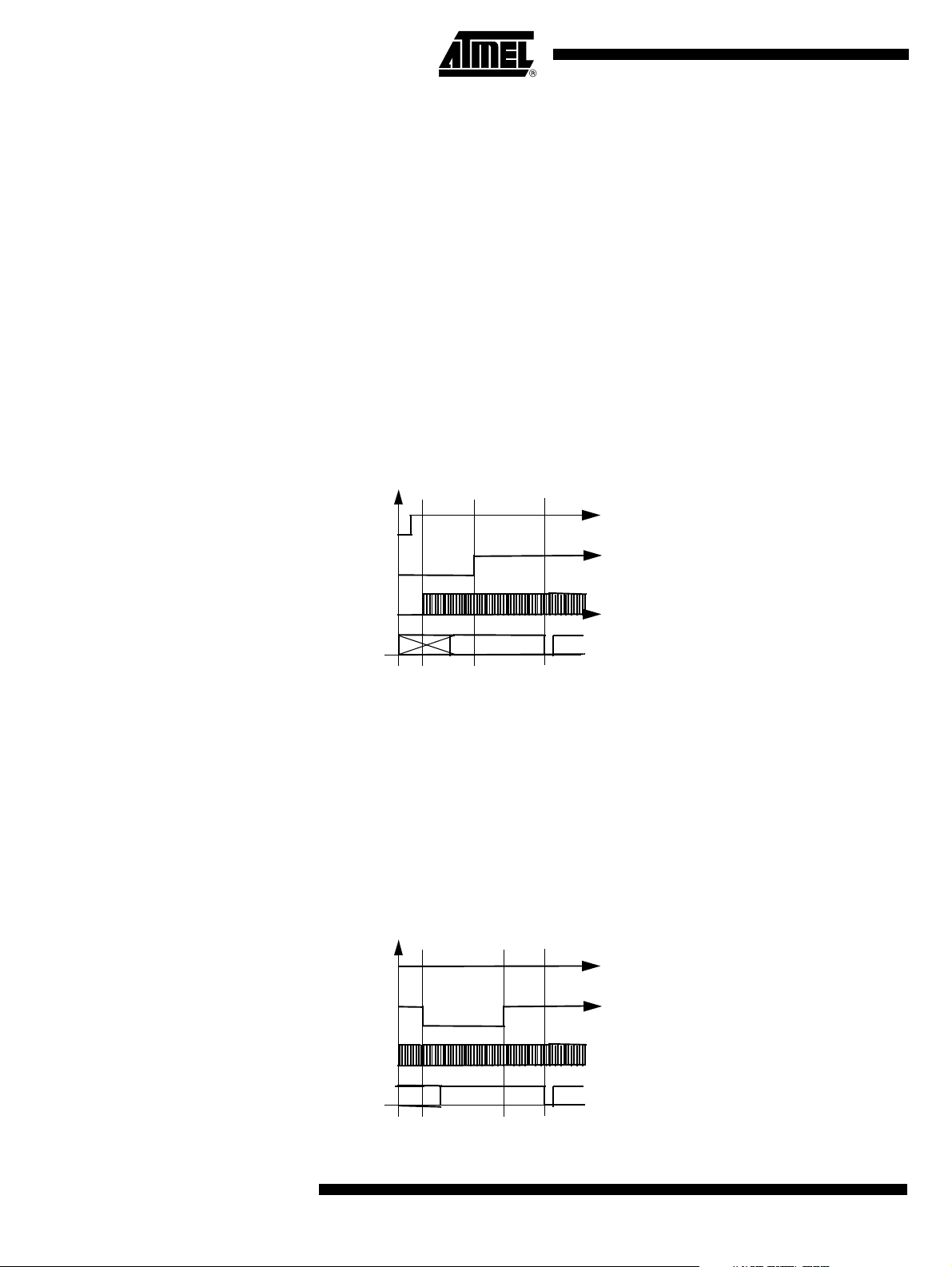
AT8xC5122/23
Power-on and Power-off FSM Th e Pow er- on P owe r-off Finite Sta te M ach ine (FS M) a pplie s th e sig nals on the sm art
card in accordance with ISO7816-3 standard. It conducts the Activation (Cold Reset and
Warm Reset as well as De-Activation) it also manages the exception conditions such as
overcurrent (see DC/DC Converter)
To be able to power on the SCIB, the card presence is mandatory. Upon detectection of
a card presence, the Terminal initiate a Cold Reset Activation.
The Cold Reset Activation Terminal procedure is as follow and the Figure 37. Timing
indications are given according to ISO IEC 7816
– RESET= Low , I/O in the receive state
– Power Vcc (see DC/DC Converter)
– Once Vcc is established, apply Clock at time Ta
– Maintain Reset Low until time T a+tb (tb< 400 clocks)
– Monitor The I/O line for the Answer To Reset (ATR) between 400 and 40000
clock cycles after Tb. ( 400 clocks < tc < 40000clocks)
Figure 37. SCIB Activation Cold Reset Sequence after a Card Insertion
CVCC
CRST
CCLK
CIO
Ta Ta+tb
DataUndefined
Tb+tc
The Warm Reset Activation Terminal procedure is as follow and the Figure 38
– Vcc active, Reset = High, CLK active
– Terminal drive Re set low at time T to init ia t e the w ar m Reset. Reset=0
maintained for at least 400 clocks until time Td = T+te (400 clocks < te)
– Terminal keep the IO line in receive state
– Terminal drive Reset high after at least 400 clocks at time Td
– ICC shall respond with an ATR within 40000 clocks (tf<40000 clocks)
Figure 38. SCIB Activation Warm Reset Sequence
CVCC
72
CRST
CCLK
CIO
Undefined
T Td=T + te
Data
Td + tf
4202E–SCR–06/06
Page 73

AT8xC5122/23
Removal of the smart card will automatically start the power off sequence as described
in Figure 39.
The SCIB deactivation sequence after a reset of the CPU or after a lost of power supply
is ISO7816-3 co mpliant. The s witching ord er of the signal s is the sam e as in Figu re 39
but the delay between signals is analog and not clock dependant.
Figure 39. SCIB Deactivation Sequence after a Card Extraction
CVCC
CRST
CCLK
8 Clock Cycles
CIO
Interrupt Gen e rator There are several sourc es of interrup tion but the SCIB m ac ro-cell issues onl y o ne inter-
rupt signal: SCIBIT.
Figure 40. SCIB Interrupt Sources
Transmit bu ffe r
copied to shift register
Output current
out of range
Output voltage
out of range
Timeout on WT
counter
Complete
transmission
Complete
reception
Parity error
detected
ESCTBI
ICARDER
EVCARDER
ESCWTI
ESCTI
ESCRI
ESCPI
SCTBI
ICARDERR
VCARDERR
SCWTI
SCTI
SCRI
SCPI
SCIB IT
4202E–SCR–06/06
This signal is high level active. Each of the sources is able to activate the SCIB interruption which is cleared when the Smart Card Interrupt register is read by the
microcontroller.
If during the read of the Smart Card Interrupt register another interrupt occurs, the activation of th e corr es pond ing b it in t he Sm art Ca rd I nterru p t regi ste r and t he new S CI B
interruption is delayed until the interrupt register is read by the microcontroller.
Warning : Each bit of the SCIIR register is irre levant whi le the corresp ond ing interr uption is disabled in SCIER register. When the interruption mode is not used, the bits of
the SCISR register must be used instead of the bits of the SCIIR register.
73
Page 74

AT8xC5122/23
Additional Features
Clock The CK_ISO input must be in the range 1 - 5 MHz according to ISO 7816.
The CK_ISO can b e program m ed up t o 1 2 M H z. In this c ase, the timin g spec ification of
the output buffer will not comply to ISO 7816.
Figure 41. Clock Diagram of the SCIB Block
CK_IDLE
CK_PLL or
CK_XTAL1
PR2
Ck_cpu
Ck_ISO
SCIB
Figure 42. Prescaler 2 Description
PR2
<48
CK_ISO
=48
SCICLK[5:0]
XTSCS
SCICLK.7
EXT48
PLLCON.2
CK_PLL
CK_XTAL1
0
1
1/(2*(48 - SCICLK[5-0]))
The divi sion f act or SC ICLK m ust be sm all er than 4 9. If it is g reat er or eq ua l to 49, t he
PR2 prescaler is locked.
See Figure 17 clock tree diagram in the clock controller chapter.
Table 42. Examples of Clock settings
XTAL1 (MHz) EXT48 SCICLK CK_ ISO
80 36 4
80 44 12
80 42 8
80 40 6
80 24 2
80 0 1
Card Presence Input The internal pull-up (weak pull-up) on Card Presence input can be disconnected in order
to reduce the consumption (CPRESRES , bit 3 in PMOD0).
Ω
In this case, an external resistor (typically 1 M
) must be externally tied to Vcc.
CPRES input can generate an interrupt (see Interrupt system section).
The detection level can be selected.
74
4202E–SCR–06/06
Page 75

AT8xC5122/23
Transmit / Receive Buffer The contents of the SCIBUF Transmit / Receive Buffer is transferred or received into /
from the Shift Register. The Shift Register is not accessible by microcontroller. Its role is
to prepare the byte to be copied on the I/O pin for a transmission or in the SCIBUF
buffer after a reception.
During a character transmission proc ess, as s oon a s the contents of the SCIBUF buffer
is transferred to the shift register, the SCTBE bit is set in SCISR register to indicate that
the SCIBUF buffer i s em pty a nd ready to acce pt a new byte. This mechanism a voids t o
wait for the complete transmission of the previous byt e before writing a new byte in the
buffer and enables to speed up the transmission.
– If the Character repetition mode is not selected (bit CREP=0 in SCICR), as
soon as the contents of the Shift Register is transferred to I/O pin, the SCTC
bit is set in SCISR register to indicate that the byte has been transmitted.
– If the Character repetition mode is selected (bit CREP=1 in SCICR) The
TERMINAL will be able to repeat characters as requested by the ICC (See
the Parity Error in T=0 protocol description in the definition paragraph
above). The SCTC bit in SCISR register will be set after a successful
transmission (no retry or no further retry requested by the ICC). If the
number of retries is exhausted (up to 4 retries depending on CREPSEL bit i n
SCSR) and the last retry is still unsuccessful, the SCTC bit in SCISR will not
be set and the SCPE bit in SCISR register will be set instead.
During a character reception process, the conten ts of the Shift Registe r is transferred in
the SCIBUF buffer.
– If the Character repetition mode is not selected (bit CREP=0 in SCICR), as
soon as the contents of the Shift Register is transferred to the SCIBUF the
SCRC bit is set in SCISR register to indicate that the byte has been
received, and the SCIBUF contains a valid character ready to be red by the
microcontroller.
– If the Character repetition mode is selected (bit CREP=1 in SCICR) The
TERMINAL will be able to request repetition if the received character exhibit
a parity error. Up to 4 retries can be requested depending on CREPSEL bit
in SCSR. The SCRC bit will be set in SCISR register after a successful
reception, first reception or after retry(ies). If the number of retries is
exhausted (up to 4 retries depending on CREPSEL bit in SCSR) and the last
retry is still unsuccessful, the SCRC bit and the SCPE bit in SCISR register
will be set. It will be possible to read the erroneous character.
Warning : the SCTBI, SCTI SCRI and SCPI bits have the same function as SCTBE,
SCTC, SCRC and SCPE bits. The first ones are able to generate interruptions if the
interruptions are enabled in SCIER register while the second ones are only status bits to
be used in pulling mode. If the interruption mode is not used, the status bits must be
used. The SCTBI, SCTI and SCRI bits do not contain valid information while their
respective interrupt enable bits ESCTBI, EXCTI, ESCRI are cleared.
4202E–SCR–06/06
75
Page 76
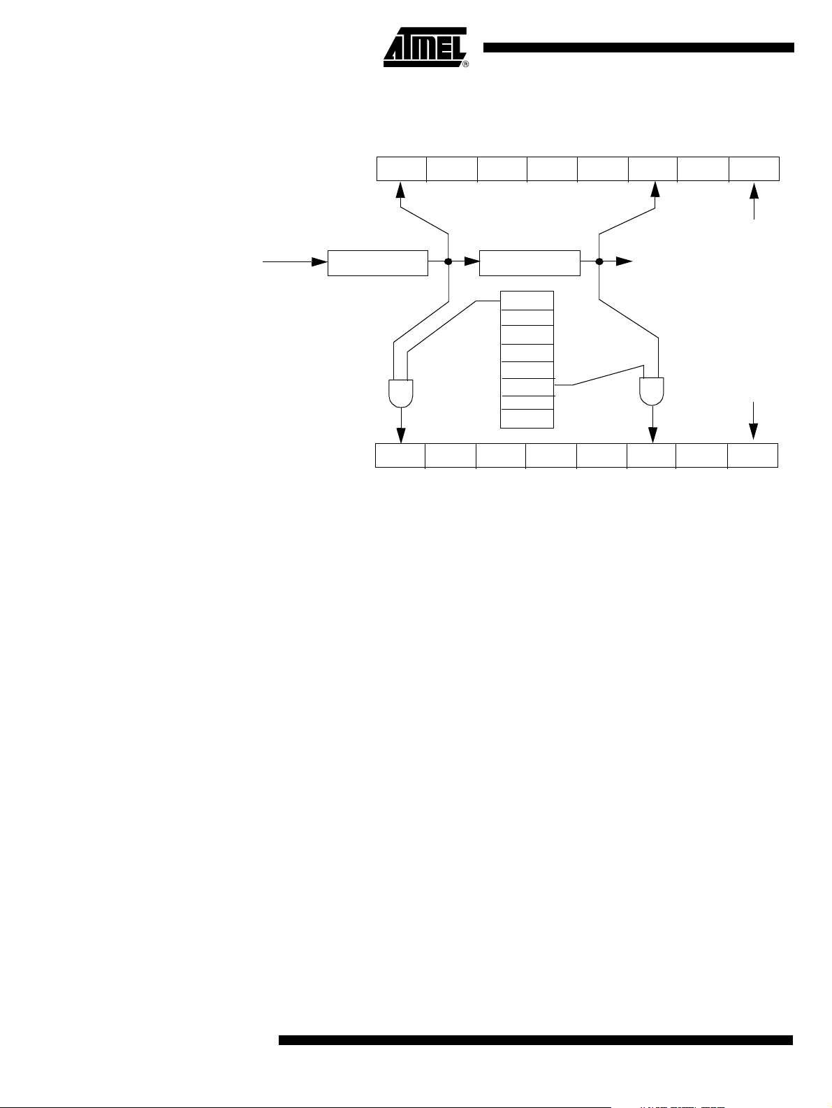
AT8xC5122/23
Figure 43. CharacterT rans m ission Diagra m
SCISR register
SCTBE
SCTC
SCPE
Transmitted
Character
SCIBUF
SCTBI
SCIIR register
Shift Register
ESCTBI
ESCTI
SCIER Register
I/O pin
SCTI
Parity error
Parity error
SCPI
76
4202E–SCR–06/06
Page 77
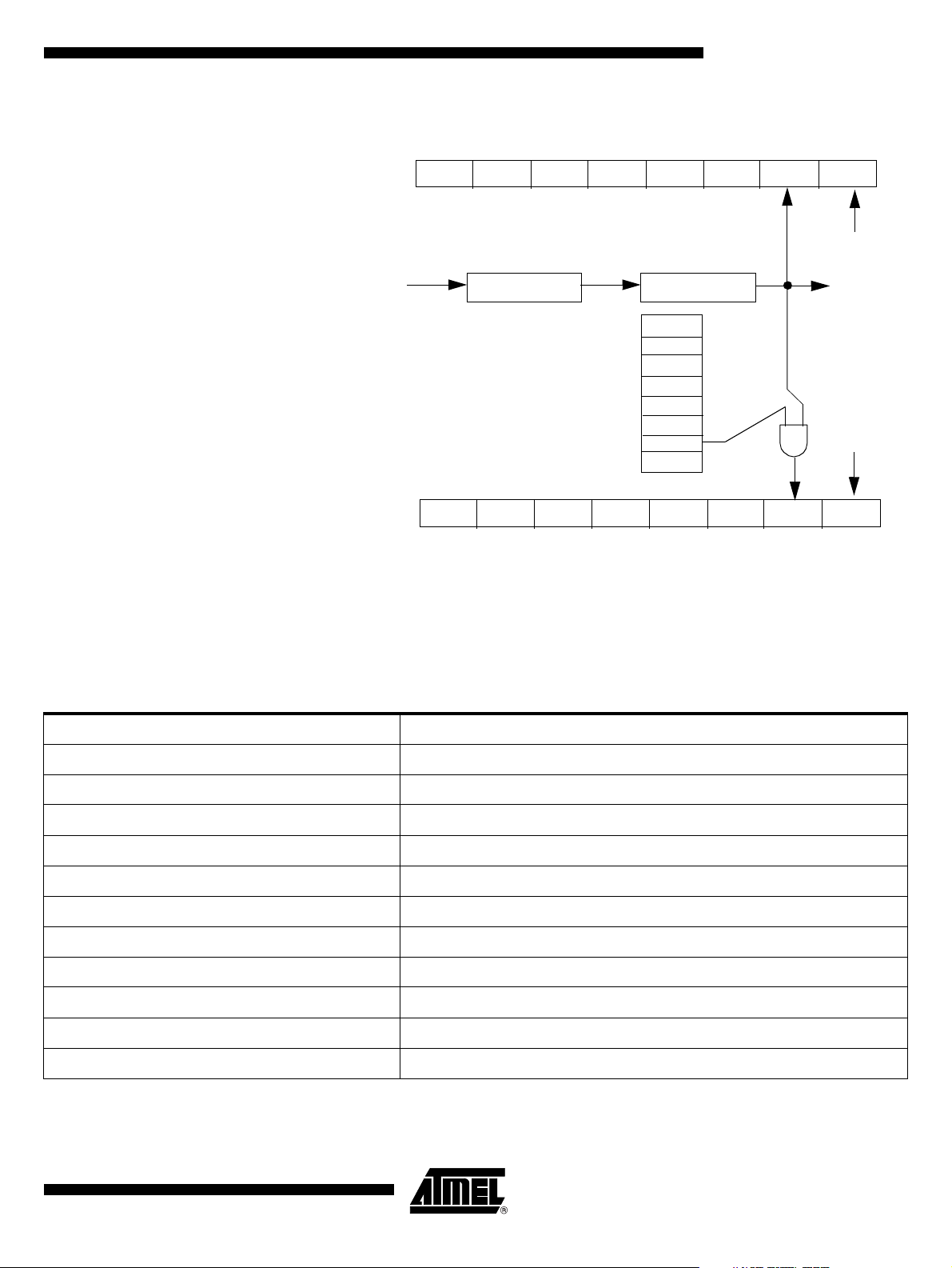
Figure 44. Character Reception Diagram
r
SCISR register
SCTBE
AT8xC5122/23
SCTC
SCRC
SCPE
Parity error
Received
I/O pin
Shift Register
SCIBUF
Characte
ESCTBI
SCTBI
SCIER Register
ESCTI
ESCRI
SCTI
SCRI
Parity error
SCPI
SCIIR register
SCIB Reset The SCICR register contains a reset bit. If set, this bit generates a reset of the SCIB and
its registers. Table 43 defines the SCIB registers that are reset and their reset values.
Table 43. Reset Values for SCI Registers
Register Name SCIB Reset Value (Binary)
SCICR 0000 0000
SCCON 0X00 0000
SCISR 1000 0000
SCIIR 0X00 0000
SCIER 0X00 0000
SCSR X000 1000
SCIBUF 0000 0000
SCETU1, SCETU0 XXXX X001, 0111 0100 (372)
SCGT1, SCGT0 0000 0000, 0000 1100 (12)
SCWT3, SCWT2, SCWT1, SCWT0 0000 0000, 0000 0000, 0010 0101, 1000 0000 (9600)
SCICLK 0X10 1111
4202E–SCR–06/06
77
Page 78
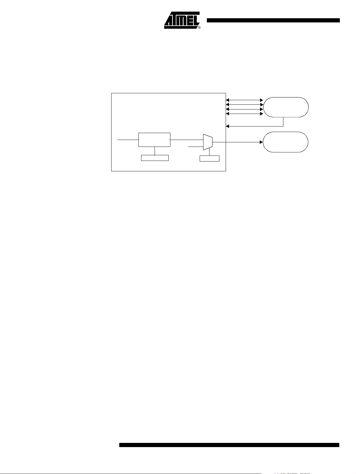
AT8xC5122/23
Alternate Card A second card named ‘Alternate Card’ can be controlled.
The Clock signal CCLK1 can be adapted to the XTAL frequency. Thanks to the clock
prescaler which can divide the frequency by 1, 2, 4 or 8. The bits ALTKPS0 and
ALTKPS1 in SCSR Register are used to set this factor.
Figure 45. Alternate Card
CVCC
CRST
CIO
CCLK
CPRES
SMART
CARD
Main
card
Registers
CK_IDLE
PR3
ALTKPS0,1
SCSR Reg.
1, 1/2, 1/4 or 1/8
P1.7
1
0
SCCLK1
SCSR R eg.
CCLK1
SIM, SAM
CARD
Alternate
card
There are fifteen registers to control the SCIB macro-cell. They are described from
Table 58 to Table 45.
Some of the register widths are greater than a byte. Despite the 8 bits access provided
by the BIU, the address mapping of this kind of register respects the following rule :
The Low significant byte register is implemented at the higher address.
This implementation makes access to these registers easier when using high level pro-
gramming languages (C,C++).
78
4202E–SCR–06/06
Page 79

AT8xC5122/23
Table 44. Smart Card Interface Control Register - SCICR (S:B6h, SCRS = 1)
76543210
RESET CARDDET VCARD1 VCARD0 UART WT EN CREP CONV
Bit Number Bit Mnemonic Description
Reset
7 RESET
6 CARDDET
5-4 VCARD[1:0]
Set this bit to reset and deactivate the Smart Card Interface.
Clear this bit to activate the Smart Card Interface.
This bit acts as an active high software reset.
Card Pr esence D etector Sense
Clear this bit to indicate the card presence detector is open when no card is inserted (CPRES is high).
Set this bit to indicate the card presence detector is closed when no card is inserted (CPRES is low).
Card Voltage Selection:
VCARD[1]
VCARD[0] CVCC
00 0 V
01 1.8 V
10 3.0 V
1 1 5.0 V
3UART
2WTEN
1 CREP
0CONV
Reset Value = 0000 0000b
Card UART Selection
Clear this bit to use the CARDIO bit (P1.0) bit to drive the Card I/O (P1.0) pin.
Set this bit to use the Smart Card UART to drive the Card I/O pin (P1.0 pin).
Contr ols also the Waiting T ime Counter as described in S ection “Waiting Time (WT) C ounter”, page 69
Waiting Time Counter Enable
Clear this bit to stop the counter and enable the load of the Waiting Time co unter hold regist ers.
The hold regist ers are l oaded with SCWT0, SCWT1, SCWT 2 and SCWT3 values when SCWT2 is written.
Set this bit to start the Waiting Time Counter. The counters stop when it reaches the timeout value.
If the UART bit is set, the Waiting Time Counter automatically reloads with the hold registers whenever a start bit is
sent or received.
Character Repetition
Clear this bit to disabl e parit y error detection and indication on the Card I/O pin in receive mode and to disable
charac ter repetitio n in transmit mode.
Set this bit to enable parity error indication on the Card I/O pin in receive mode and to set automatic character
repetition when a parity error is indicated in transmit mode.
Depending upon CREPSET bit is SCSR register, the receiver can indicate parity error up to 4times (3 repetitions) or
up to 5times (4 repetitions) after which it will raise the parity error bit SCPE bit in the SCISR register. If parity interrupt
is enabled, the SCPI bit in SCIIR register will be set too.
Alternately, the transmitter will detect ICC character repetition request. After 3 or 4 unsuccessful repetitions
(depending on CREPSEL bit in SCSR register), the transmitter will raise the parity error bit SCPE bit in the SCISR
register. If parity interrupt is enabled, the SCPI bit in SCIIR regist er will be set too.
Note : Character repetition mode is specified for T=0 protocol onl y and should not be used in T=1 protocol (block
oriented protocol)
ISO Convention
Clear this bit to use the direct convention: b0 bit (LSB) is sent first, the parity bit is added after b7 bit and a low level
on the Card I/O pin represents a’0’.
Set this bit to use the inverse convention: b7 bit (LSB) is sent first, the parity bit is added after b0 bit and a low level on
the Car d I/O pin r epresents a’1’.
4202E–SCR–06/06
79
Page 80

AT8xC5122/23
Table 45. Smart Card Contacts Register - SCCON (S:ACh, SCRS=0)
76543210
CLK - CARDC8 CARDC4 CARDIO CARDCLK CARDRST CARDVCC
Bit Number Bit Mnemonic Description
Card Clock Selection
7CLK
Clear this bit to use the Card CLK bit (CARDCLK bit below) to drive Card CLK (P1.4) pin.
Set this bit to use CK_XTAL1 or CK_PLL signals for CK_ISO to drive the Card CLK pin (CCLK = P1.4 pin)
Note: internal synchro nization avoids g litches on the CLK pi n when switching this bit.
6-
5 CARDC8
4 CARDC4
3 CARDIO
2 CARDCLK
1 CARDRST
Reserved
This bit can be changed by software but the read value is indeterminate.
Card C8
Clear this bit to drive a low level on the Card C8 pin (CC8 = P1.1 pin).
Set this bit to s et a high level on the Card C8 pin (CC8 = P1 .1 pin)..
The CC8 pin can be used as a pseudo bi- directi onal I/O w hen this bit is set.
Warning : VCARDOK=1 (SCISR.4 bit) condition must be true to change the state of CC8 pin
Card C4
Clear this bit to drive a low level on the Card C4 pin (CC4 = P1.3 pin).
Set this bit to s et a high level on the Card C4 pin (CC4 = P1.3 pin).
The CC4 pin can be used as a pseudo bi- directi onal I/O w hen this bit is set.
Warning : VCARDOK=1 (SCISR.4 bit) condition must be true to change the state of CC4 pin
Card I/O
If UART bit is cleared in SCICR register, this bit enables the use of the Card IO pin (CIO = P1.0) as a C51
pseudo bi-directional port :
To read from CIO (P1.0) port pin : set CARDIO (P1.0) bit then read CARDIO (P1.0) bit to have the CIO port
value
To writ e in CIO (P1.0) po rt pi n : se t CARDI O (P1 .0 ) bit to writ e a 1 in CI O ( P1. 0 ) port pin , clea r CARDI O (P 1.0)
bit to write a 0 in CIO (P1.0) port pin.
Warning : VCARDOK=1 (SCISR.4 bit) condition must be true to change the state of CIO pin
Card CLK
When the CLK bit is cleared in SCCON Register, the value of this bit is driven to the Card CLK pin.
Warning : VCARDOK=1 (SCISR.4 bit) condition must be true to change the state of Card CLK pin
Card RST
Clear this bit to drive a low level on the Card RST pin.
Set this bit to s et a high level on the Card RST pin.
Warning : VCARDOK=1 (SCISR.4 bit) condition must be true to change the state of Card RST pin
0 CARDVCC
Reset Value = 0X00 0000b
80
Card VCC Control
Clear this bit to desactivate the Card interface and set its power-off. The other bits of SCCON register have no
effect while thi s bit is cl ea red .
Set this bit to pow er-on the C ard interface. The activa tion sequence shou ld be handled by software.
4202E–SCR–06/06
Page 81

AT8xC5122/23
Table 46. Smart Card UART Interface Status Register -
SCISR (S:ADh, SCRS=0)
76 5 4 32 10
SCTBE CARDIN ICARDOVF VCARDOK SCWTO SCTC SCRC SCPE
Bit Number Bit Mnemonic Description
UART Transmit Buffer Empty Status
7SCTBE
6 CARDIN
5 ICARDOVF
4 VCARDOK
This bit is set by hardware when the Transmit Buffer is copied to the transmit shift register of the Smart Card
UART.
It is cleared by hardware when SCIBUF register is written.
Card Presence Status
This bit is set by hardware if there is a card presence (debouncing filter has to be done by software).
This bit is cleared by hardware if there is no card presence.
Card Current Overflow Status
This bit is set when the current on card is above the limit specified by bit OVFADJ in DCCKPS register (Table 61
on page 94)
It is cleared by hardware.
Card Voltage Correct Status
This bit is set when the output voltage is within the voltage range specified by VCARD[1:0] in SCICR register.
It is cleared otherwise.
3SCWTO
2SCTC
1SCRC
0SCPE
Reset Value = 1000 0000b
Waiting Time Counter Timeout Status
This bit is set by hardware when the Waiting Time Counter has expired.
It is cleared by the reload of the counter or by the reset of the SCIB.
UART Transmitted Character Status
This bit is s et by hard war e when the S ma rt C ar d UA RT ha s tr an smit te d a char act er. If c ha ract e r re pe tit io n mo de is
selected, this bit will be set only after a successful transmission. If the last allowed repetition in not successful, this
bit will not be set.
It is cleared by so ftware when this register is read.
UART Received Character Status
This bit is set by hardware when the Smart Card UART has received a character
It is cleared by hardware when SCIBUF register is read. If character repetition mode is selected, this bit will be set
only after a successful reception. If the last allowed repetition is still unsuccessful, this bit will be set to let the user
read the er ro neous value if ne ce s sa r y.
Character Reception Parity Error Status
This bit is set whe n a parity error is de tec ted on the recei ve d ch ar ac t er.
It is cleared by software when this register is read. If character repetition mode is selected, this bit will be set only
if the ICC report an error on the last allowed repetition of a TERMINAL transmission, or if a reception parity error
is foun d on the last allowe d IC C character repetition.
4202E–SCR–06/06
81
Page 82

AT8xC5122/23
Table 47. Smart Card UART Interrupt Identification Register (Read Only)
SCIIR (S:AEh, SCRS=0)
765 4 3 2 1 0
SCTBI - ICARDERR VCARDERR SCWTI SCTI SCRI SCPI
Bit Number Bit Mnemonic Description
UART Transmit Buffer Empty Interrupt
7SCTBI
This bit is set by hardware when the Transmit Buffer is copied into the transmit shift register of the Smart
Card UART. It generates an inte rrupt if ESCTBI bit is set in SCIER register otherwise th is bit is irre levant.
It is cleared by hardware when this register is read.
6-
5 ICARDERR
4 VCARDERR
3SCWTI
2SCTI
1 SCRI
0SCPI
Reset Value = 0X00 0000b
Reserved
The value read from this bit is indeterminate. Do not change this bit.
Card Current Overflow Interrupt
This bit is set when the current on card is above the limit specified by bit OVFADJ in DCCKPS register (Table
61 on page 94). It generates an interrupt if ICARDER bit is set in SCIER register otherwise this bit is
irrelevant.
It is cleared by hardware when this register is read.
Card Voltage Error Interrupt
This bit is set when the output volta ge goes out of the voltage range specified by VCARD field. It gener ates
an interrupt if EVCARDER bit is set in SCIER register otherwise this bit is irrelevant.
It is cleared by hardware when this register is read.
Waiting Time Counter Timeout Interrupt
This bit is set by hardware when the Waiting Time Counter has expired. It generates an interrupt if ESCWTI
bit is set in SCIER register otherwise this bit is irrelevant.
It is cleared by hardware when this register is read.
UART Transmitted Character Interrupt
This bit is set by hardware when the Smart Card UART has completed the character transmission. It
generates an interrupt if ESCTI bit is set in SCIER register otherwise this bit is irrelevant.
It is cleared by hardware when this register is read.
UART Received Character Interrupt
This bit is set by hardware when the S mart Card UART has completed the c haracter reception. It generates
an interrupt if ESCRI bit is set in SCIER register otherwise this bit is irrelevant.
It is cleared by hardware when this register is read.
Character Reception Parity Error Interrupt
This bit is set at the same time as SCTI or SCRI if a parity error is detected on the received character. It
generates an interrupt if ESCPI bit is set in SCIER register otherwise this bit is irrelevant.
It is cleared by hardware when this register is read.
Note: 1) In case of multiple interrupts occuring at the same t ime (sampled by the same edge of
the internal clock), the interrupts will be serviced in the following order from the highest t o
the lowest priority :
-
UART Transmit Buffer Empty
- Card Current Overflow
- Card Vo ltage Error
- Waiting Time Counter Timeout
- UART Transmi tt e d C ha racter
- UART Received Character
- Character Reception Parity Error
82
2) It is recommended that the application saves the SCIIR register after reading it in
order to avoid the loss of pending interru ptions as the SCIIR register is cleared when it is
read by the MC U .
4202E–SCR–06/06
Page 83

AT8xC5122/23
Table 48. Smart Card UART Interrupt Enabling Register - SCIER (S:AEh, SCRS=1)
765 4 3210
ESCTBI - ICARDER EVCARDER ESCWTI ESCTI ESCRI ESCPI
Bit Number Bit Mnemonic Description
UART Transmit Buffer Empty Interrupt Enabled
7 ESCTBI
Clear this bit to disable the Smart Card UART Transmit Buffer Empty interrupt.
Set this bit to enable the Smart Card UART Transmit Buffer Empty interrupt.
6-
5 ICARDER
4 EVCARDER
3ESCWTI
2 ESCTI
1 ESCRI
0ESCPI
Reset Value = 0X00 0000b
Reserved
The value read from this bit is indeterminate. Do not change this bit.
Card Current Overflow Interrupt Enabled
Clear this bit to disable the Card Current Overflow interrupt.
Set this bit to enable the Card Current Overflow interrupt.
Card Voltage Error Interrupt Enabled
Clear t his bit to disabl e the Card Voltage Error interrupt.
Set this bit to enable the Card Voltage Error interrupt.
WaitingTime Counter Timeout Interrupt Enabled
Clear this bit to disable the Waiting Time Counter timeout interrupt.
Set this bit to enable the Waiting Time Counter timeout interrupt.
UART Transmitted Character Interrupt Enabled
Clear this bit to disable the Smart Card UART Transmitted Character interrupt.
Set this bit to enable the Smart Card UART Transmitted Character interrupt.
UART Received Character Interrupt Enabled
Clear this bit to disable the Smart Card UART Received Character interrupt.
Set this bit to enable the Smart Card UART Received Character interrupt.
Character Reception Parity Error Interrupt Enabled
Clear this bit to disable the Smart Card Character Reception Parity Error interrupt.
Set this bit to enable the Smart Card Character Reception Parity Error interrupt.
4202E–SCR–06/06
83
Page 84

AT8xC5122/23
Table 49. Smart Card Selection Register - SCSR (S:ABh)
76543210
- BGTEN - CREPSEL ALTKPS1 ALTKPS0 SCCLK1 SCRS
Bit Numb er Bit Mn em o ni c Descriptio n
7-
6BGTEN
5-
4 CREPSEL
3-2 ALTKPS1:0
1 SCCLK1
0 SCRS
Reset Value = X000 1000b
Reserved
The val ue read from this bit is inde terminate. Do no t change this bit.
Block Guard Time Enabl e
Set this bit to s elect the minimum i nterval between t he leading edge of the start bits of the last chara c ter
received from the ICC and the first character sent by the Terminal. The transfer of GT[8-0] value to the BGT
counter is done on the rising edge of the BGTEN.
Clear this bit to suppress the minimum time between reception and transmission.
Reserved
The val ue read from this bit is inde terminate. Do no t change this bit.
Character repetition selection
Clear this bit to select 5 times transmission (1 original + 4 repetitions) before parity error indication (conform to
EMV)
Set this bit to select 4 times transmission (1 original + 3 repetitions) before parity error indication
Alternate Card Clock prescaler factor
00 ALTKPS = 0: prescaler f actor equ als 1
01 ALTKPS = 1: prescaler factor equals 2
10 ALTKPS = 2: prescaler factor equals 4 (reset value)
11 ALTKPS = 3: prescaler factor equals 8
Alternate card cloc k selectio n
Set to se lect the prescaled PR3 clock for CCLK1 (P1.7) pin
Clear to select P1.7 port bit
Smart Car d R eg i st er Selection
The SCRS bit selects which set of the SCIB registers is accessed.
Table 50. Smart Card Transmit / Re ce ive Buffer - SCIBUF (S:AA)
76543210
- -------
Bit Number Bit Mnemonic Description
Smart Card Transmit / R eceive B uffer
- A new byte can be written in the buffer to be transmitted on the I/O pin when SCTBE bit is set.
--
The bits are sorted and copied on the I/O pin versus the active convention.
- A new byte received from I/O pin is ready to be read when SCRI bit is set.
The bits are sorted versus the activ e convention.
Reset Value = 0000 0000b
84
4202E–SCR–06/06
Page 85

AT8xC5122/23
Table 51. Smart Card ETU Register 1 - SCETU1 (S:ADh, SCRS=1)
76543210
COMP----ETU10ETU9ETU8
Bit Number Bit Mnemonic Description
Compensation
7COMP
Clear this bit when no time compensation is needed (i.e. when the ETU to Card CLK period ratio is close to an
integer with an error less than 1/4 of Card CLK period).
Set this bit otherwise and reduce the ETU period by 1 Card CLK cycle for even bits.
6-3 -
2-0 ETU[10:8]
Reserved
The val ue read from these bits is indeterminate. Do not change these bits.
ETU MSB
Used together with the ETU LSB in SCETU0 (Table 52)
Warning : the ETU counter is reloaded at each register’s write operation.
Do not change this register during character reception or transmission or while Guard Time or Waiting Time
Counters are running.
Reset Value = 0XXX X001b
Table 52. Smart Card ETU Register 0 - SCETU0 (S:ACh, SCRS=1)
76543210
ETU7 E TU6 ETU5 ETU4 ETU3 ETU2 ETU1 ETU0
Bit Number Bit Mnemonic Description
ETU LSB
7 - 0 ETU[7:0]
The Elementary Time Unit is (ETU[10:0] - 0.5*COMP)/f, where f is the Card CLK frequency.
According to ISO 7816, ETU[10:0] can be set between 1 1 and 2048 (2047 ?)
The default reset value of ETU[10:0] is 372 (F=372, D=1).
Reset Value = 01 11 0100b
4202E–SCR–06/06
85
Page 86

AT8xC5122/23
Table 53. Smart Card Transmit Guard Time Register 0 - SCGT0 (S:B4h, SCRS=1)
76543210
GT7 GT6 GT5 GT4 GT3 GT2 GT1 GT0
Bit Number Bit Mnemonic Description
T ransmit Guard Time LSB
The minimum time between two consecutive start bits in transmit mode is GT[8:0] * ETU. This is equal to ISO IEC
7 - 0 GT[7:0]
Reset Value = 0000 1100b
Table 54. Smart Card Transmit Guard Time Register 1 - SCGT1 (S:B5h, SCRS=1)
76543210
-------GT8
Bit Number Bit Mnemonic Description
Guard Time +10 (see Guard Time Counter description.
According to ISO IEC 7816,the time between 2 consecut ive leading edge st art bits can be set between 11 and
266 (11 to 254+12 ET Us) .
7 - 1 -
0GT8
Reserved
The val ue read from these bits is indeterminate. Do not change these bits.
T ransmit Guard Time MSB
Used together with the Transmit Guard Time LSB in SCG T0 register (Table 53).
Reset Value = XXXX XXX0b
Table 55. Smart Card Character/Block Waiting Time Register 3
SCWT3 (S:C1h, SCRS= 0)
76543210
WT31 WT30 WT29 WT28 WT27 WT26 WT25 WT24
Bit Number Bit Mnemonic Description
7 - 0 WT[31:24]
Waiting Time Byte3
Used together with WT[2 3:0] in registers SCWT2,SCWT1, SCWT0 (see Table 56).
Reset Value = 0000 0000b
86
4202E–SCR–06/06
Page 87

AT8xC5122/23
Table 56. Smart Card Character/Block Waiting Time Register 2
SCWT2 (S:B6h, SCRS=0)
76543210
WT23 WT22 WT21 WT20 WT19 WT18 WT17 WT16
Bit Number Bit Mnemonic Description
7 - 0 WT[23:16]
Waiting Time Byte2
Used together with WT[3 1:24] and WT[15:0] in registers SCWT 3,SCWT1, SCWT0 (se e Table 58).
Reset Value = 0000 0000b
Table 57. Smart Card Character/Block Waiting Time Register 1
SCWT1 (S:B5h, SCRS=0)
76543210
WT15 WT14 WT13 WT12 WT11 WT10 WT9 WT8
Bit Number Bit Mnemonic Description
7 - 0 WT [15:8]
Waiting Time Byte 1
Used together with WT[31:16] and WT[7:0] in registers SCWT3,SCWT2, SCWT0 (see Table 55).
Reset Value = 0010 0101b
Table 58. Smart Card Character/Block Waiting Time Register 0
SCWT0 (S:B4h, SCRS=0)
76543210
WT7 WT6 WT5 WT4 WT3 WT2 WT1 WT0
Bit Number Bit Mnemonic Description
Waiting Time Byte 0
WT[31:0] is the reload va lue of the Waiting Time Counter ( WTC).
7 - 0 WT[7: 0]
The WTC is a general-purpose timer. It is using the ETU clock and is controlled by the WTEN bit (see Table 44 on
page 79 and Section “Waiting Time (WT) Counter”, page 69).
When UART bit of Registers is set, the WTC is automatically reload ed at each start bit of the UART. It is used to
check the maximum time between to consecutive start bits.
Reset Value = 1000 0000b
4202E–SCR–06/06
87
Page 88

AT8xC5122/23
Table 59. Smart Card Clock Reload Register - SCICLK (S:C1h, SCRS=1)
7 6 543210
XTSCS - SCICLK5 SCICLK4 SCICLK3 SCICLK2 SCICLK1 SCICLK0
Bit Number Bit Mnemonic Description
Smart Card Clock Selection Bit
7XTSCS
If XTSCS bit is set OR EXT48 bit is set (in PLLCON register) , CK_PLL is used to generate CK_ISO.
Otherwise, CK_XTAL1 is used to generate CK_ISO.
See the C lock Tree diagram figure 17.
6-
5 - 0 SCICLK[5: 0]
Reserved
The value read from this bit is indeterminate. Do not change these bits.
SCIB clock reload register
Prescaler 2 reload value is used to defines the card clo ck frequency.
If SCICLK[5:0] is smaller than 48 :
Fck_is o = Fck_pll or Fck_XTAL1/ (2 * (48 - SCI CLK[5:0 ]))
If SCICLK[5:0] is equal to 48 :
Fck_iso = Fck_XTAL1
SCICLK[5:0] must be smaller than 49.
Reset Value = 0X10 1111b (default value for a divider by two)
DC/DC Converter The Smart Card voltage (CVCC) is supplied by the integrated DC/DC converter which is
controlled by several registers:
• The SCICR register (Table 44 on page 79) controls the CVCC level by means of bits
VCARD[1:0].
• The SCCON register (Table 45 on page 80) enables to switch the DC/DC converter
on or off by means of bit CARDVCC.
• The DCCKPS register (Table 61 on page 94) controls the DC/DC clock and current.
The DC/DC co nverter ca nnot be sw itched o n while th e CPRES pi n rema ins inacti ve. If
CPRES pin becomes inactive while the DC/DC converter is operating an automatic shut
down sequence of the DC/DC converter is initiated by the electronics.
It is mandatory to switch off the DC/DC Converter before entering in Power-down mode.
Configuration The DC/DC Conv erter can work in two different modes which are selected by bit MODE
in DCCKPS register:
• Pump Mode: an external inductance of 10 µH must be connected between pins LI
and VCC. VCC can be higher or lower than CVCC.
• Regulator mode : no external inductance is required but VCC must be always higher
than CVCC+0.3V. The Regulation mode will work even if an external inductance of
10 µH is connected between pins LI and VCC
The DC/DC clock prescaler which is controlled by bits DCCKPS[3:0], in DCCKPS register must be confi gured to set the DC/DC cloc k to a w orking frequenc y of 4 MHz w hich
depends upon the value of the crystal. There is no need to change the default configuration set by the reset sequence if an 8 MHz crystal is used by the application.
The DC/DC Converter implements a current overflow controller which avoids permanent
damage of the DC/DC converter in case of short circuit between CVCC and CVSS. The
maximum limit is around 100 mA. It is possible to increase this limit in normal operating
88
4202E–SCR–06/06
Page 89

AT8xC5122/23
mode by 20% by means of bit OVFADJ in DCCKPS register. When the current overflow
controller is operating, the ICARDOVF is set by the hardware in SCISR register.
The curren t dra wn fr om po wer s upply by th e DC/ DC con verte r is c ontroll ed du ring th e
startup phase in order to avoid hig h tran sient cu rrent mainly in P um p Mo de which could
cause the power sup ply vo ltage to drop dram atic ally. Th is cont rol is don e by mea ns of
bits BOOST[1:0], which increases progressively the startup current level.
Initializat i on P rocedure The initialization procedure is different depending upon the required Card Vcc. One pro-
cedure apply for Card Vcc =< 3 volts and one procedure for Card Vcc = 5 volts.
The initialization procedure involves :
• Select the CVCC level by means of bits VCARD[1:0] in SCICR register,
• Set bits BOOST[1:0] in DCCKPS register following the current level control wanted.
• Switch the DC/DC on by means of bit CARDVCC in SCCON register,
• Monitor bit VCARDOK in SCISR register in order to know when the DC/DC
Converter is ready (CVCC voltage has reached the expected level)
Procedure for CVcc =< 3 volts The DC/DC regulation mode must be selected for Card Vcc = 1.8 volts and Card Vcc =
3 volts (MO DE = 1 in DCC KPS regi ster) The detailed procedur es is des cribed in flo w
chart of Figure 46. for Card Vcc = 1.8 v olts and i n the flow chart o f Figure 47. for Card
Vcc = 3 volts
4202E–SCR–06/06
89
Page 90

AT8xC5122/23
Figure 46. Card Vcc = 1.8V Initialization Procedure
SCICR.7=Reset=1
SCICR.7=Reset=0
VCARD[1:0] = 01
Mode Regulation
DCCKPS[7]=1
BOOST[1:0]=01
SCCON CardVcc=1
Set Timeout to 3 ms
VCARDOK=1
Timeout
Expired
DC/DC Initialization
Failure
DC/DC Initialization
successful
90
4202E–SCR–06/06
Page 91

Figure 47. Card Vcc = 3V Initialization Procedure
SCICR.7=Reset=1
SCICR.7=Reset=0
VCARD[1:0] = 10
Mode Regulation
DCCKPS[7]=1
BOOST[1:0]=01
SCCON CardVcc=1
Set Timeout to 3 ms
AT8xC5122/23
VCARDOK=1
Timeout
Expired
DC/DC Initialization
Failure
DC/DC Initialization
successful
4202E–SCR–06/06
91
Page 92
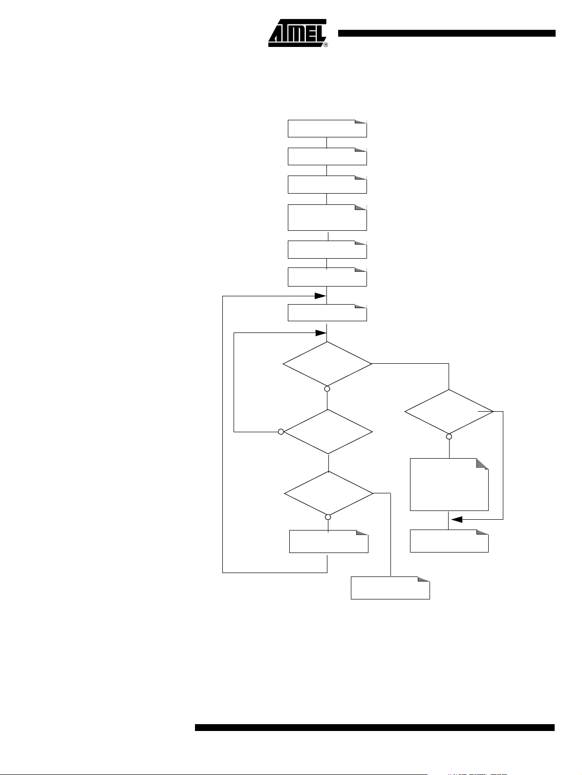
AT8xC5122/23
Procedure for CVcc = 5volts The DC/DC pump mode must be selected (MODE = 0 in DCCKPS register). The
detailed procedure is described in flow chart of Figure 48.
Figure 48. Card Vcc = 5V Initialization Procedure
SCICR.7=Reset=1
SCICR.7=Reset=0
VCARD[1:0] = 11
Mode Pump
DCCKPS[7]=0
BOOST[1:0]=[0:0]
SCCON CardVcc=1
Set Timeout to 3 ms
VCARDOK=1
BOOST[1:0]
Timeout
Expired
BOOST[1:0]
= max = 3?
Increment
BOOST [1:0]
DC/DC Initialization
Failure
= [0:0]
Decrement
BOOST[1:0]
to adjust the
current overflow
DC/DC Initialization
Successful
While VCC remains higher than 4.0V and startup current lower than 30 mA (depending
on the load type), the DC/DC converter should be ready without having to increment
BOOST[1:0] bits beyond [0:0] level. If VCC > 4.0V and startup current > 30 mA, it will be
necessary to increment the BOOST[1:0] bits until the DC/DC converter is ready.
92
Incrementation of BOOST[1:0] bits increases at the same time the current overflow level
in the same proportion as the startup current. So once the DC/DC converter is ready it is
4202E–SCR–06/06
Page 93
AT8xC5122/23
advised to decrem ent the BOO ST[1:0] bits to restore the overflo w current t o its norma l
or desired value.
Monitoring Procedure Once the DC/DC has b een s ucces sfuly in itialized, it is neces sary t o m oni tor the DC/ DC
converter by means of bits VCARDOK and ICARDOVF in the SCISR register.
Table 60. DC/DC converter status
VCARDOK ICARDOVF DC/DC Status
- Not Started or switched off by application.
The curr ent overflow sensor is disab led during the DC/DC converter startu p. Then if a current
overflow condition is applied during the DC/DC converter startup, the DC/DC converter is unable
00
0 1 Started and automatically switched off by a current overflow condition
1 0 Operating properly accor ding to ISO/IEC 7816-3 and EMV recomm endations
to start and both bits VCARDOK and ICARDOVF remains at 0.
DC/DC converter correctly started then the output voltage is out of ISO/IEC 7816-3
specifications. In this case the firmware must take appropriate actions like deactivating the
DC/DC converter in compliance with ISO/IEC 7816.
1 1 Not applicable
4202E–SCR–06/06
93
Page 94

AT8xC5122/23
DC/DC Converter register
Table 61. DC/DC Converter Control Register - DCCKPS (S:BFh)
76543210
MODE OVFADJ BOOST1 BOOST0 DCCKPS3 DCCKPS2 DCCKPS1 DCCKPS0
Bit Number Bit Mnemonic Description
Regulation mode
7MODE
6 OVFADJ
0 : Pump mode (External Inductance required)
1 : Regulator mode (No Exte rnal inductance required if VCC > CV CC+0.3V)
Current O ver fl ow Adju s tm ent on Sm art Car d terminal
0 : normal: 100 mA average
1 : normal + 20%
VCARDOK=0 VCARDOK=1
5 - 4 BOOST[1:0]
3 - 0 DCCKPS[3:0]
Reset Value = 0000 0000b
Maximum Startup Current drawn from power supply
00 : Normal: 30 mA average
01 : Normal + 30%
10 : Normal + 50%
11 : Normal + 80%
DC/DC Clock Prescaler Value
0000 : Division factor: 2 (reset value)
0001 : Division factor: 3
0010 : Division factor: 4
0011 : Division factor: 5
0100 : Division factor: 6
0101 : Division factor: 8
01 10 : Division factor: 10
0111 : Division factor: 12
1000 : Division factor: 24
Other values are reserved
Current Ove rflow Level on Smar t Car d terminal
00 : Normal = OVFADJ
01 : Normal + 30%
10 : Normal + 50%
11 : Normal + 80%
94
4202E–SCR–06/06
Page 95

AT8xC5122/23
USB Controller The A T8xC5122D implement s a USB device c ontroller supportin g Full Speed da ta
transfer. In addition to the default control endpoint 0, it provides 6 other endpoints, which
can be configured in Control, Bulk, Interrupt or Isochronous modes:
• Endpoint 0: 32-byte FIFO, default control endpoint
• Endpoint 1,2,3: 8-byte FIFO
• Endpoint 4,5: 64-byte FIFO
• Endpoint 6: 2 x 64-byte Ping-pong FIFO
This allows the firmware to be developed conforming to most USB device classes, for
example:
• USB Mass Storage Class Control/Bulk/Interrupt (CBI) Transport, Revision 1.0 December 14, 1998.
• USB Mass Storage Class Bulk-Only Transport, Revision 1.0 - September 31, 1999.
• USB Human Interface Device Class, Version 1.1 - April 7, 1999.
• USB Device Firmware Upgrade Class, Revision 1.0 - May 13, 1999.
USB Mass Storage Classes
USB Mass Storage Class CBI Transport
USB Mass Storage Class BulkOnly Transport
USB Device Firmware Upgrade (DFU)
Within the CBI framework, the Control endpoint is used to transport command blocks as
well as to transport standard US B reque sts. One Bulk-Out endpoint is used to transport
data from the host to the device. One Bulk-In endpoint is used to transport data from the
device to the host. And one interrupt endpoint may also be used to signal command
completion (protocol 0); it is optional and may not be used (protocol 1).
The following configuration adheres to these requirements:
• Endpoint 0: 8 bytes, Control In-Out
• Endpoint 4: 64 bytes, Bulk-Out
• Endpoint 5: 64 bytes, Bulk-In
• Endpoint 1: 8 bytes, Interrupt In
Within the Bulk-Only framework, the Control endpoint is only used to transport classspecific and s tandard US B reques ts for devi ce set- up and con figura tion. One B ulk-Out
endpoint is used to transport commands and data from the host to the device. One BulkIn endpoint is used to transport status and data from the device to the host. No interrupt
endpoint is needed.
The following configuration adheres to these requirements:
• Endpoint 0: 8 bytes, Control In-Out
• Endpoint 4: 64 bytes, Bulk-Out
• Endpoint 5: 64 bytes, Bulk-In
The USB Device Firmwa re Upda te (DFU) protocol c an be used to upgrad e the on-chi p
program memory of the AT8xC5122D. This allows the implementation of product
enhancements and patches to devices that are already in the field. Two different configurations and description sets are used to support DFU functions. The Run-Time
configuration co-exists with the usual functions of the devic e, which may be USB Mas s
Storage for the AT8xC5122D. It is used to initiate DFU from the normal operating mode.
The DFU configuration is used to perform the firmware update after device re-configuration and USB reset. It excludes any other function. Only the default control pipe
(endpoint 0) is used to support DFU services in both configurations.
4202E–SCR–06/06
95
Page 96

AT8xC5122/23
r
The only p ossi ble va lue for the wMa xPac ketSiz e in th e DFU co nfi gurat ion is 32 b ytes ,
which is the size of the FIFO implemented for endpoint 0.
Description The USB device controller provides the hardware that the AT8xC5122D and the
AT83C5123 need to interface a USB link to a data flow stored in a double port memory
(DPRAM).
The US B co ntroll er requ ires a 48 M Hz r eferen ce cl ock, w hich i s the outpu t of th e
AT8xC5122D/23 PLL (see Section "Phase Lock Loop (PLL)", page 42) divided by a
clock prescaler. This clock is used to generate a 12 MHz full speed bit clock from the
received USB d ifferential data and to transmit data according t o full speed USB devic e
tolerance. Clock recovery is done by a Digital Phase Loc ked Loop (DP LL) block, which
is compliant with the jitter specification of the USB bus.
The Interface Engine (SIE) block performs NRZI encoding and decoding, bit stuffing,
CRC generation and checking, and the serial-parallel data conversion. The Universal
Function Interface (UFI) performs the interface between the data f low and the Dual Port
Ram
Figure 49. USB Device Controller Block Diagram
48 MHz +/- 0.25%
D+
DPLL
USB
12MHz
D+/D-
D-
Buffer
SIE
Serial Interface Engine (SIE) The SIE performs the following functions:
• NRZI data encoding and decoding.
• Bit stuffing and unstuffing.
• CRC generation and checking.
• Handshakes.
• TOKEN type identifying.
• Address checking.
• Clock generation (via DPLL).
C51
Microcontrolle
Interface
UFI
Up to 48 MHz
UC_SYSCLK
96
4202E–SCR–06/06
Page 97

Figure 50. SIE Block Diagram
r
End of Pack et
Detection
AT8xC5122/23
SYNC detection
PID decoder
Address Decoder
Serial to Parallel
Conversion
CRC5 & CRC16
Generation/Check
8
Dat aIn [7 :0]
DataOut
8
D+
D-
Start of Packet
Detection
Clock
Recovery
Clk48
(48 MHz)
NRZI ‘ NRZ
Bit Unstuffing
Packet bit counter
SysClk
(12 MHz)
USB Pattern Ge nerator
Parallel to Serial Converter
Bit Stuffing
NRZI Converter
CRC16 Generator
Function Interface Unit (UFI) The Function Interface Unit provides the interface between the AT8xC5122D (or
AT83C5123) and the SIE. It manages transactions at the packet level with minimal intervention from the device firmware, which reads and writes the endpoint FIFOs.
Figure 51. UFI Block Diagram
UFI
DPLL
Transfer
Control
FSM
SIE
DPR Control
USB side
Asynchronous Information
Transfer
Endpoint 6
Endpoint 5
Endpoint 4
Endpoint 3
Endpoint 2
Endpoint 1
Endpoint 0
User DPRAM
CSREG 0 to 7
Registers
Bank
DPR Control
mP side
C51
Microcontrolle
Interface
Up to 48 MHz
UC_SYSCLK
4202E–SCR–06/06
97
Page 98

AT8xC5122/23
Figure 52. Minimum Intervention from the USB Device Firmware
OUT Transactions:
HOST
UFI
C51
IN Transactions:
HOST
UFI
C51
OUT DATA0 (n Bytes)
IN
NACK
Endpoi nt F IF O wr it e
ACK
interrupt C51
Endpoint FIFO read (n bytes)
IN
DATA1
OUT DATA1
OUT DATA1
NACK
IN
DATA1
ACK
interrupt C51
Endpoint FIFO write
ACK
98
4202E–SCR–06/06
Page 99

Configuration
General Configuration • USB controller enable
Before any USB transaction, the 48 MHz required by the USB controller must be correctly generated (Section "Clock Controller", page 41).
The USB controller should be then enabled by setting the USBE bit in the USBCON
register.
• Set address
After a Reset or a USB reset, the software has to set the FEN (Function Enable) bit in
the USBADDR register. This action will allow the USB controller to answer to the
requests sent at the address 0.
When a SET _ADDRE SS request has be en receive d, the USB con troller must on ly
answer to the address defined by the request. The new addres s should be st ored in the
USBADDR register. The FEN bit and the FADDEN bit in the USBCON register should
be set to allow the USB controller to answer only to requests sent at the new address.
• Set configuration
The CONFG bit in the USBCON regist er should be set after a SET_CO NFIGUR ATION
request with a non-zero value. Otherwise, this bit should be cleared.
AT8xC5122/23
Endpoint Configuration • Selection of an Endpoint
The endpoint register access is performed using the UEPNUM register. The following
registers
correspond to the endpoint whose numbe r is stored in the UEPNUM register. To select
an Endpoint, the firmware has to write the endpoint number in the UEPNUM register.
– UEPSTAX,
– UEPCONX,
–UEPDATX,
–UBYCTX,
Figure 53. Endpoint Selection
Endpoint 0
Endpoint 6
UEPSTA0 UEPCON0 UEPDAT0
UBYCT0
UEPSTA6 UEPCON6 UEPDAT6
UBYCT6
0
SFR Registers
1
2
X
3
4
UEPSTAX UEPCONX UEPDATX
UBYCTX
5
6
4202E–SCR–06/06
UEPNUM
99
Page 100

AT8xC5122/23
• Endpoint enable
Before using an endpoint, this one should be enabled by setting the EPEN bit in the
UEPCONX register.
An endpoint which is not enabled won’t answer to any USB request. The Default Control
Endpoint (Endpoint 0) should always be enabled in order to answer to USB standard
requests.
• Endpoint type configuration
All Standard Endpoints can be configured in Control, Bulk, Interrupt or Isochronous
mode. The Ping-pong Endpoints can be configured in Bulk, Interrupt or Isochronous
mode. The configuration of an endpoint is performed by setting the field EPTYPE with
the following values:
– Contro l: EPTYPE = 00b
– Isochronou s: EPTYPE = 01b
– Bulk: EPTYPE = 10b
– Interrupt: EPTYPE = 11b
The Endpoint 0 is the Default Control Endpoint and should always be configured in Control type.
• Endpoint direction configuration
For Bulk, Int errup t and Isochro nous en dpo ints, th e direct ion is define d with t he EP DIR
bit of the UEPCONX register with the following values:
– IN:EPDIR = 1b
– OUT:EPDIR = 0b
For Control endpoints, the EPDIR bit has no effect.
• Summary of Endpoint Configuration:
Make sure to select the correct endpoint number in the UEPNUM register before
accessing to endpoint specific registers.
Table 62. Summary of Endpoint Configuration
Endpoint configurati on EPEN EPDIR EPTYPE UEPC ON X
Disabled 0b Xb XXb 0XXX XXXb
Control 1b Xb 00b 80h
Bulk-In 1b 1b 10b 86h
Bulk-Out 1b 0b 10b 82h
Interrupt-In 1b 1b 11b 87h
100
Interrupt-Out 1b 0b 11b 83h
Isochronous-In 1b 1b 01b 85h
Isochronous-Out 1b 0b 01b 81h
4202E–SCR–06/06
 Loading...