

Page 1

Features
• Secure battery authentication
• Superior SHA-256 Hash Algorithm
• Best in class 256 bit key length
• Guaranteed Unique 48 bit Serial Number
• High speed single wire interface
• Supply Voltage: 2.5 – 5.5V
• <100nA Sleep Current
• 4KV ESD protection
• Green compliant (exceeds RoHS) 3 pin SOT-23 package
CryptoAuthentication™
Applications
• Cell Phones
• PDA and Smart Phones
• Portable Media Players
• Digital Cameras & Camcorders
• Cordless Tools
• Handheld Devices
1. Introduction
The AT88SA100S is a small authentication chip that can be used to
validate battery packs and other replaceable items that contain a
power source. It uses the industry leading SHA-256 hash algorithm
to provide the ultimate level of security.
An industry leading key length of 256 bits prevents exhaustive
attacks while multiple physical security features prevent
unauthorized disclosure of the secret key stored within the chip.
This key is automatically erased when power is removed from the
device.
It is shipped with a guaranteed unique 48 bit serial number that is
used in combination with an input challenge and the stored secret
key to generate a response that is unique for every individual
device.
The chip also includes 80 one-time fuses that can be used to
configure the system and/or retain permanent status. The values in
these fuses can also be locked to prevent modification.
AT88SA100S
Battery Authentication
Chip
Preliminary
8558A–SMEM–03/09
Page 2

1.1. Memory Resources
Sram 256 bits of SRAM that are used for storage of a key. The LoadSram command provides a
mechanism to securely initialize this block during personalization. This memory will retain its value
when the chip is put/goes to sleep, so long as a supply voltage in excess of V
the chip.
MemValid A single bit that tells whether or not Sram contains valid data. It’s cleared when power is lost and set
when the SRAM is loaded with a secret key.
Fuse Block of 128 fuse bits that can be read and written through the 1 wire interface. The first 8 bits are
lock bits that control burn ability on 16 bit words of the array. Fuse[88-95] are manufacturing ID
values fixed by Atmel. Fuse[96-127] are programmed by Atmel with a serial number that (in
combination with MaskSN) is guaranteed to be unique and which includes lot/wafer info.
ROM Metal mask programmed memory. Unrestricted reads are permitted on the first 64 bits of this array.
The physical ROM will be larger and will contain other information that cannot be read.
ROM MfrID 2 bytes of ROM that, when combined with Fuse[88:95] specifies the 24 bit manufacturing
ID code (MfrID). This value is assigned by Atmel and is always the same for all chips of a
particular model number. For the AT88SA100S, this value is 0xFF FF FF. The MfrID can
be read by accessing ROM bytes 0 & 1 of Address 0. The 24 bit MfrID value can always
be read by the system and is always included in the message digested by the MAC
command.
ROM SN 2 bytes of ROM that can be used to identify chips among others on the wafer. These bits
reduce the number of fuses necessary to construct a unique serial number. The ROM SN
is read by accessing ROM bytes 2 & 3 of Address 0. The complete serial number is
extended with an additional 32 fuses to form the 48 bit serial number. The serial number
can always be read by the system and is optionally included in the message digested by
the MAC command.
RevNum 4 bytes of ROM that are used by Atmel to identify the design revision of the AT88SA100S
chip. These bytes can be freely read as the four bytes returned from ROM address 1,
however system code should not depend on this value as it may change from time to time.
is still supplied to
RETAIN
1.2. Fuse Map
The AT88SA100S chip incorporates 128 one-time fuses within the chip. Once burned, there is no way to reset the
value of a fuse. Fuses, with the exception of the manufacturing ID and serial number bits, initialized by Atmel, have a
value of 1 when shipped from the Atmel factory and transition to a 0 when they are burned.
Table 1. The 128 fuses in the AT88SA100S chip are arranged in the following manner:
Fuse # Name Description
0 – 7 Fuse Lock Bits Each bit locks the current value of the corresponding 16 bit block of the fuse array,
see below for more details.
8 Æ 87 Status Fuses These fuses can be written with the BurnFuse command and can always be read
with the Read command.
88 Æ 95 MfrID See Section 1.1. Set by Atmel, can’t be modified in the field
96 Æ 127 Serial Number See Section 1.1. Set by Atmel, can’t be modified in the field
Fuse Lock Bits These 8 fuses can be used to prevent further writing of the status fuses. Bit 0, when burned, locks
Fuse[0-15] from being modified, Bit[1] locks Fuse[16-31] and so on up through bit 5, which locks
Fuse[80-87]. Fuse[88-127] can never be modified with the BurnFuse command. Note that burning bit
0 has the effect of preventing any changes to the current value of the lock bits.
2 AT88SA100S [Preliminary]
8558A–SMEM–03/09
Page 3

AT88SA100S [ Preliminary]
Status Fuses These fuses can be used to store various information which is not secret. Their value can always be
determined using the Read command. They can be individually burned using the BurnFuse
command. Two common usage models for these fuses are:
1. Consumption logging, i.e. burn one bit after every n uses, the host system keeps track of the
number of uses so far for this serial number since the last fuse burn.
2. Model number information. In this situation, the bits are written at the factory and their value is
locked to prevent modifications in the field. This method can also be used for feature enabling.
1.3. SHA-256 Computation
This chip performs only one cryptographic calculation – a keyed digest of an input challenge using the SHA-256
algorithm, documented here:
http://csrc.nist.gov/publications/fips/fips180-2/fips180-2.pdf
1.3.1. SHA Computation Example
In order to ensure that there is no ambiguity, the following example vector is provided in addition to the sample vectors
in the NIST document. In this example, all values are listed in hex. For all but the key, bytes are listed in the order that
they appear on the bus – first on the left. Key is listed in the same order, so the 01 at the left of the key string is the first
byte passed to SHA-256.
Key 01030507090B0D0F11131517191B1D1F21232527292B2D2F31333537393B3D3F
Challenge 020406080A0C0E10121416181A1C1E20222426282A2C2E30323436383A3C3E40
Opcode 01
Mode 40 (include serial number in message)
Param2 0000
MfrID Fuses 77
S/N Fuses 8899AABB
MfrID ROM CCDD
MaskSN ROM EEFF
The 88 bytes over which the digest is calculated are 0103…3D3F0204…3E4001400000…EEFF
Digest: 7D38245733717A488575B9F794F7BCAFE033A3848D39430DA25141FDEBEAA1C2
A Read command executed on address 0 of the ROM (MfrID ROM, MaskSN ROM) would return CC DD EE FF, with
CC being the first byte on the bus and FF being the last.
Throughout this document, the complete message processed by the SA100S chip is documented. According to the
above specification, this always includes a single bit of ‘1’ pad after the message, followed by a 64 bit value
representing the total number of bits being hashed (less pad and length). If the length is less than 447 (512-64-1) then
the necessary number of ‘0’ bits are included between the ‘1’ pad and ‘length’ to stretch the last message block out to
512 bits.
When using standard libraries to calculate the SHA-256 digest, these pad and length bits should probably not be
passed to the library as most standard software implementations of the algorithm add them in automatically.
3
8558A–SMEM–03/09
Page 4
1.4. Security Features
This chip incorporates a number of physical security features designed to protect the key from unauthorized release.
These include an active shield over the entire surface of the internal memory encryption, internal clock generation,
glitch protection, voltage tamper detection and other physical design features.
Both the clock and logic supply voltage are internally generated, preventing any direct attack via the pins on these two
signals.
2. IO Protocol
Communications to and from this chip take place over a single asynchronously timed wire using a pulse count scheme.
The overall communications structure is a hierarchy:
Table 2. IO Hierarchy
Tokens
Flags
Blocks
Packets
2.1. IO Tokens
There are a number of IO tokens that may be transmitted along the bus:
Input: (To device)
Wake Wake device up from sleep (low power) state
Zero Send a single bit from system to the device with a value of 0
One Send a single bit from system to the device with a value of 1
Output: (From the device)
ZeroOut Send a single bit from the device to the system with a value of 0
OneOut Send a single bit from the device to the system with a value of 1
The waveforms are the same in either direction, however there are some differences in timing based on the expectation
that the host has a very accurate and consistent clock while the device has significant variation in its internal clock
generator due to normal manufacturing and environmental fluctuations.
The bit timings are designed to permit a standard UART running at 230.4K baud to transmit and receive the tokens
efficiently. Each byte transmitted or received by the UART corresponds to a single bit received or transmitted by the
device. Refer to Applications Notes on Atmel’s website for more details describing how the UART should be controlled.
Implement a single data bit transmitted on the bus, or the wake-up event.
Comprised of eight tokens (bits) which convey the direction and meaning of the next group of bits (if any)
which may be transmitted.
of data follow the command and transmit flags. They incorporate both a byte count and a checksum to
ensure proper data transmission
of bytes form the core of the block without the count and CRC. They are either the input or output
parameters of a AT88SA100S chip command or status information from the AT88SA100S chip
4 AT88SA100S [Preliminary]
8558A–SMEM–03/09
Page 5
AT88SA100S [ Preliminary]
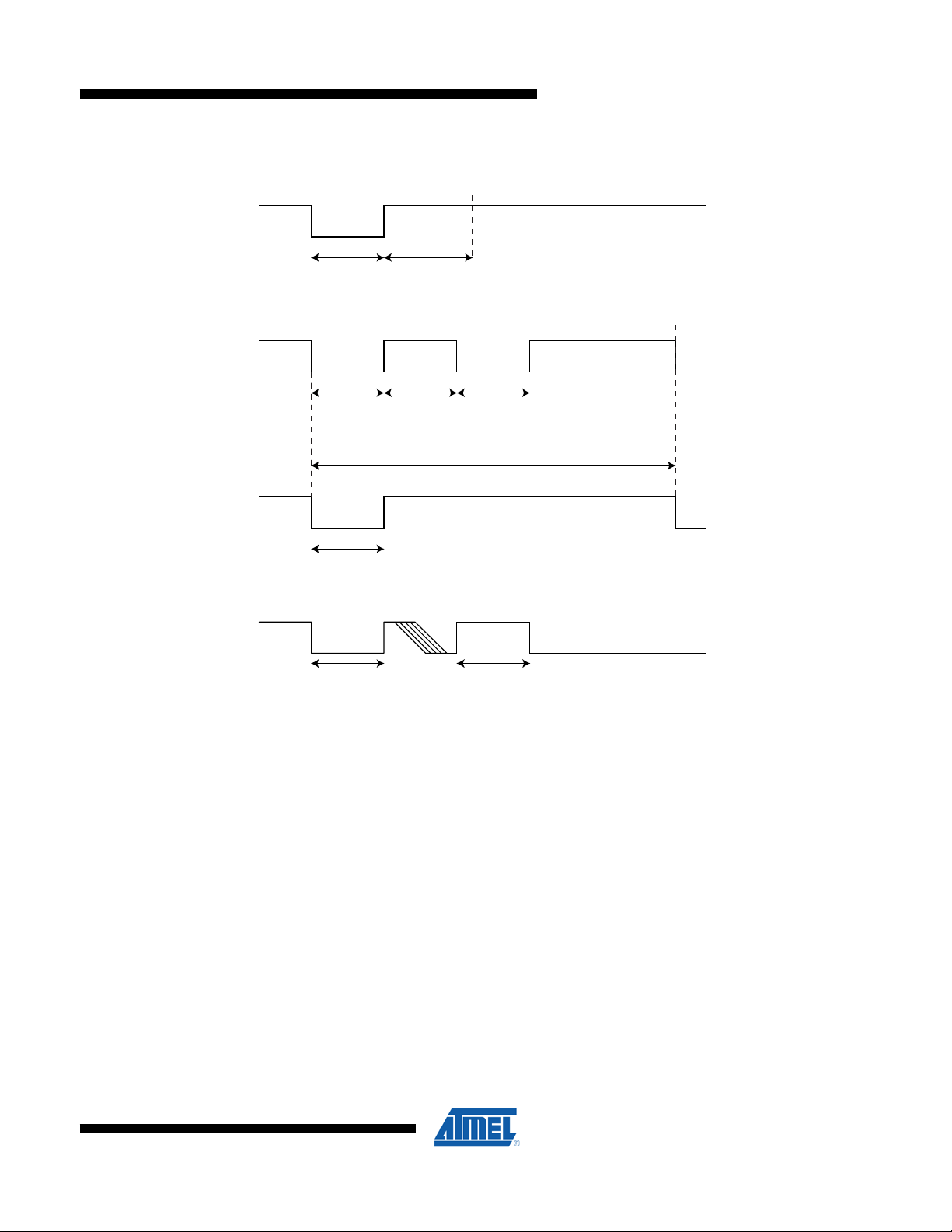
2.2. AC Parameters
Figure 1. AC Parameters
data commWAKE
LOGIC Ø
LOGIC 1
NOISE
SUPPRESION
t
WLO
t
START
t
START
t
LIGNORE
t
WHI
t
ZHI
t
ZLO
t
BIT
t
HIGNORE
8558A–SMEM–03/09
5
Page 6
μ
μ
μ
μ
μ
μ
μ
μ
μ
μ
μ
μ
μ
Table 3. AC Parameters
Parameter Symbol Direction Min Typ Max Unit Notes
Wake Low
Duration
Wake Delay to
Data Comm.
Start pulse
duration
Zero
transmission
t
WLO
t
WHI
t
START
t
ZHI
high pulse
Zero
transmission
t
ZLO
low pulse
(1)
Bit time
Turn around
delay
High side
glitch filter @
t
BIT
t
TURNAROUND
t
HIGNORE_A
active
Low side glitch
filter @ active
High side
glitch filter @
t
LIGNORE_A
t
HIGNORE_S
sleep
Low side glitch
filter @ sleep
IO Timeout
Watchdog
reset
t
LIGNORE_S
t
TIMEOUT
t
WATCHDOG
Note 1: START, ZLO, ZHI & BIT are designed to be compatible with a standard UART running at 230.4K baud for both
transmit and receive.
To
CryptoAuthentication
To
CryptoAuthentication
To
CryptoAuthentication
From
CryptoAuthentication
To
CryptoAuthentication
From
CryptoAuthentication
To
CryptoAuthentication
From
CryptoAuthentication
To
CryptoAuthentication
From
CryptoAuthentication
From
CryptoAuthentication
To
CryptoAuthentication
To
CryptoAuthentication
To
CryptoAuthentication
To
CryptoAuthentication
To
CryptoAuthentication
To
CryptoAuthentication
To
CryptoAuthentication
60 -
1 - ms Signal should be stable high for this
4.1 4.34 4.56
4.62 6.0 8.6
4.1 4.34 4.56
4.62 6.0 8.6
4.1 4.34 4.56
4.62 6.0 8.6
37.1 39 -
46.2 60 86
46.2 60 86
46.2 60 86
45 ns Pulses shorter than this in width will be
45 ns Pulses shorter than this in width will be
2
2
7 10 13 ms Starting as soon as 7ms up to 13ms after
374 500 650 ms Max. time from wake until chip is forced
Signal can be stable in either high or low
s
levels during extended sleep intervals.
entire duration.
s
s
s
s
s
s
s
If the bit time exceeds t
TIMEOUT
then
CryptoAuthentication will enter sleep
mode and the wake token must be
resent.
s
CryptoAuthentication will initiate the first
s
low going transition after this time interval
following the end of the Transmit flag
After CryptoAuthentication transmits the
s
last bit of a block, system must wait this
interval before sending the first bit of a
flag
ignored by the chip, regardless of its
state when active
ignored by the chip, regardless of its
state when active
Pulses shorter than this in width will be
s
ignored by the chip when in sleep mode
Pulses shorter than this in width will be
s
ignored by the chip when in sleep mode
the initial signal transition of a token chip
will enter sleep if no complete and valid
token is received.
into sleep mode. Refer to Watchdog
Failsafe Section 3.4
6 AT88SA100S [Preliminary]
8558A–SMEM–03/09
Page 7

AT88SA100S [ Preliminary]
3. DC Parameters
Table 4. DC Parameters
Parameter
Symbol
Min
Typ
Max Unit Notes
Operating temperature
Power Supply Voltage
Fuse Burning Voltage
Active Power Supply
Current
Sleep Power Supply
Current
Input Low Voltage @
V
= 5.5V
cc
Input Low Voltage @
V
= 2.5V
cc
Input High Voltage @
V
= 5.5V
cc
Input High Voltage @
= 2.5V
V
cc
Input Low Voltage when
Active
Input High Voltage when
Active
Output Low voltage
Output Low current
Maximum Input Voltage
ESD
T
A
V
cc
V
BURN
I
CC
I
SLEEP
V
IL
V
IL
V
IH
V
IH
V
IL
V
IH
V
OL
I
OL
V
MAX
V
ESD
-40 85 °C
2.5 5.5 V
3.8 5.5 V
Voltage is applied to Vcc pin
- 10 mA
100 nA
-0.5
.25 * V
cc
-0.5 0.5 V
.25 * V
6.0 V
cc
1.0 3.0 V
-0.5 0.8 V
1.2 6.0 V
0.4 V
4 mA
Vcc + 0.5
4 KV
When chip is in sleep mode,
Vsig = 0.0V, V
Voltage levels for wake token when chip is in
V
sleep mode
= 3.7V.
cc
Voltage levels for wake token when chip is in
sleep mode
Voltage levels for wake token when chip is in
sleep mode
Voltage levels for wake token when chip is in
sleep mode
When chip is in active mode,
V
= 2.5 – 5.5V
cc
When chip is in active mode,
V
= 2.5 – 5.5V
cc
When chip is in active mode,
V
= 2.5 – 5.5V
cc
When chip is in active mode,
V
= 2.5 – 5.5V, V
cc
= 0.4V
OL
V
Human Body Model, Sig & V
pins.
cc
8558A–SMEM–03/09
7
Page 8

3.1. IO Flags
The host system is always the bus master, so before any IO transaction, the system must first send an 8 bit flag to the
chip to indicate the IO operation that is to be performed, as follows:
Value Name Meaning
0x77 Command
0x88 Transmit
0xCC Sleep
All other values are reserved and will be ignored.
3.1.1. Command Timing
After a command flag is transmitted, a command block should be sent to the chip. During parsing of the parameters
and subsequent execution of a properly received command, the chip will be busy and not respond to transitions on the
signal pin. The delays for these operations are listed in the table below:
After this flag, the system starts sending a command block to the chip. The first bit of the
block can follow immediately after the last bit of the flag.
After a turn-around delay, the chip will start transmitting the response for a previously
transmitted command block.
Upon receipt of a sleep flag, the chip will enter a low power mode until the next wake token
is received.
Table 5. Command Timing
Parameter Symbol
ParsingDelay
MemoryDelay
FuseDelay
MacDelay
PersonalizeDelay
t
PARSE
t
EXEC_MEM
t
EXEC_FUSE
t
EXEC_MAC
t
PERSON
In this document, t
is used as shorthand for the delay corresponding to whatever command has been sent to the
EXEC
chip.
Mi
Max Unit Notes
n
0 50
50 100
150 300
15 30 ms Delay to execute MAC command
Delay to check CRC and parse opcode and parameters
μs
before an error indication will be available
Delay to execute Read, Write and/or SramLock commands
μs
Delay to execute BurnFuse commands
μs
7 15 ms Delay to execute GenPersonalizationKey or LoadSram
8 AT88SA100S [Preliminary]
8558A–SMEM–03/09
Page 9

AT88SA100S [ Preliminary]
3.1.2. Transmit Flag
The transmit flag is used to turn around the signal so that the device can send data back to the system, depending on
its current state. The bytes that the device returns to the system, depending on its current state as follows:
Table 6. Return Codes
State Description Error/Status Description
After wake, but prior to first
command
After successful command
execution
Execution error 0x0F Command was properly received but could not be executed by the
After CRC or other parsing
error
The device always transmits complete blocks to the system, so in the above table the status/error bytes result in 4
bytes going to the system – count, error, CRC x 2.
After receipt of a command block, the device will parse the command for errors, a process which takes t
(Refer to 3.1.1). After this interval the system can send a transmit token to the device – if there was an error then the
device will respond with an error code. If there is no error then the device internally transitions automatically from t
and will not respond to any transmit tokens until both delays are complete.
to t
EXEC
0x11 Indication that a proper wake token has been received by the device.
Return bytes per “Output Parameters” in Command section of this
–
0xFF Command was NOT properly received by the device and should be
document. In some cases this is a single byte with a value of 0x00
indicating success. The transmit flag can be resent to the device
repeatedly if a re-read of the output is necessary.
AT88SA100S chip. Changes in the AT88SA100S chip state or the
value of the command bits must happen before it is re-attempted.
re-issued by the system.
PARSE
PARSE
3.1.3. Sleep Flag
The sleep flag is used to transition the device to the low power state, which causes a complete reset of the device’s
internal command engine and input/output buffer. It can be sent to the device at any time when the device will accept a
flag.
To achieve the specified I
achieve I
avoid additional leakage on the input circuit of the chip.
if the sleep state of the input pin is high, the voltage on the input signal should be within 0.5V of VCC to
SLEEP
Atmel recommends that the input signal be brought below VIL when the chip is asleep. To
SLEEP
3.1.4. Pause State
The pause state is entered via the PauseLong command and can be exited only when the watchdog timer has expired
and the chip transitions to a sleep state. When in the pause state, the chip ignores all transitions on the signal pin but
does not enter a low power consumption mode.
The pause state provides a mechanism for multiple AT88SA100S chips on the same wire to be selected and to
exchange data with the host microprocessor. The PauseLong command includes an optional address field which is
compared to the values in Fuses 84-87. If the two match, then the chip enters the pause state, otherwise it continues to
monitor the bus for subsequent commands. The host would selectively put all but one AT88SA100S in the pause state
before executing the MAC command on the active chip. After the end of the watchdog interval all the chips will have
entered the sleep state and the selection process can be started with a wake token (which will then be honored by all
chips) and selection of a subsequent chip.
9
8558A–SMEM–03/09
Page 10

3.2. IO Blocks
Commands are sent to the chip, and responses received from the chip, within a block that is constructed in the
following way:
Byte
Number
0 Count Number of bytes to be transferred to the chip in the block, including count, packet and
1 to (N-2) Packet Command, parameters and data, or response. Refer to Section 4 for more details.
N-1, N Checksum CRC-16 verification of the count and packet bytes. The CRC polynomial is 0x8005, the
3.3. IO Flow
The general IO flow for a MAC command is as follows:
3. System sends wake token.
4. System sends Transmit Flag.
5. Receive 0x11 value from the device to verify proper wakeup synchronization.
6. System sends Command Flag.
7. System sends command block.
8. System waits t
9. System sends Transmit Flag. If command format is OK, the device ignores this flag because the computation
10. System waits t
11. System sends Transmit Flag.
12. Receive output block from the device, system checks CRC.
13. If CRC from the device is incorrect, indication transmission error, system resends Transmit flag.
14. System sends sleep flag to the device.
All commands other than MAC have a short execution delay. In these cases the system should omit steps 6, 7 & 8 and
replace this with a wait of duration t
Name Meaning
checksum, so this byte should always have a value of (N+1). The maximum size block is
39 and the minimum size block is 4. Values outside this range will cause unpredictable
operation.
initial register value should be 0 and after the last bit of the count and packet have been
transmitted the internal CRC register should have a value that matches that in the block.
The first byte transmitted (N-1) is the least significant byte of the CRC value so the last
byte of the block is the most significant byte of the CRC.
for the device to check for command formation errors.
PARSE
engine is busy. If there was an error, the device responds with an error code.
, Refer to 3.1.1.
EXEC
+ t
PARSE
EXEC
.
3.4. Synchronization
Because the communications protocol is half duplex, there is the possibility that the system and the device will fall out
of synchronization with each other. In order to speed recovery, the device implements a timeout that forces the device
to sleep. See Section 2.6.1.
10 AT88SA100S [Preliminary]
8558A–SMEM–03/09
Page 11

AT88SA100S [ Preliminary]
3.4.1. IO Timeout
After a leading transition for any data token has been received, the device will expect another token to be transmitted
within a t
assumes that the synchronization with the host is lost and transitions to a sleep state.
After the device receives the last bit of a command block, this timeout circuitry is disabled. If the command is properly
formatted, then the timeout counter is re-enabled with the first transmit token that occurs after t
an error in the command, then it is re-enabled with the first transmit token that occurs after t
In order to limit the active current if the device is inadvertently awakened, the IO timeout is also enabled when the
device wakes up. If the first token does not come within the t
performing any operations.
3.4.2. Synchronization Procedures
When the system and the device fall out of synchronization, the system will ultimately end up sending a transmit flag
which will not generate a response from the device. The system should implement its own timeout which waits for
t
during which time the device should go to sleep automatically. At this point, the system should send a Wake
TIMEOUT
token and after t
It may be possible that the system does not get the 0x11 code from the device for one of the following reasons:
1. The system did not wait a full t
Wake token and Transmit flag as a data bits. Recommended resolution is to wait twice the t
issue the Wake token.
2. The device went into the sleep mode for some reason while the system was transmitting data. In this case, the
device will interpret the next data bit as a wake token, but ignore some of the subsequently transmitted bits during
its wake-up delay. If any bytes are transmitted after the wake-up delay, they may be interpreted as a legal flag,
though the following bytes would not be interpreted as a legal command due to an incorrect count or the lack of a
correct CRC. Recommended resolution is to wait the t
3. There is some internal error condition within the device which will be automatically reset after a t
see below. There is no way to externally reset the device – the system should leave the IO pin idle for this interval
and issue the Wake token.
interval. If the leading edge of the next token is not received within this period of time, the device
TIMEOUT
+ t
WLO
PARSE
.
PARSE
interval, then the device will go back to sleep without
TIMEOUT
+ t
, a Transmit token. The 0x11 status indicates that the resynchronization was successful.
WHI
delay with the IO signal idle in which case the device may have interpreted the
TIMEOUT
delay and re-issue the Wake token.
TIMEOUT
EXEC
delay and re-
TIMEOUT
WATCHDOG
. If there is
interval,
3.5. Watchdog Failsafe
After the Wake token has been received by the device, a watchdog counter is started within the chip. After t
chip will enter sleep mode, regardless of whether it is in the middle of execution of a command and/or whether some IO
transmission is in progress. There is no way to reset the counter other than to put the chip to sleep and wake it up
again.
This is implemented as a fail-safe so that no matter what happens on either the system side or inside the various state
machines of the device including any IO synchronization issue, power consumption will fall to the low sleep level
automatically.
3.6. Byte and Bit Ordering
The device is a little-endian chip:
• All multi-byte aggregate elements within this spec are treated as arrays of bytes and are processed in the order
received.
• Data is transferred to/from the device least significant bit first on the bus.
• In this document, the most significant bit appears towards the left hand side of the page.
8558A–SMEM–03/09
WATCHDOG
, the
11
Page 12

4. Commands
The command packet is broken down in the following way:
Byte Name Meaning
0 Opcode The Command code
1 Param1 The first parameter – always present
2-3 Param2 The second parameter – always present
4 + Data Optional remaining input data
If a command fails because the CRC within the block is incorrect, the opcode is invalid or one of the parameters is
illegal, then immediately after t
packet. The value of that byte will be either 0x0F or 0xFF depending on the source of the error. See Section 2.3.2.
If a command is received successfully then after the appropriate execution delay the system will be able to retrieve the
output block as described in the individual command descriptions below.
In the individual command description tables below, the Size column describes the number of bytes in the parameter
documented in each particular row. The total size of the block for each of the commands is fixed, though that value is
different for each command. If the block size for a particular command is incorrect, the chip will not attempt the
command execution and return an error.
the system will be able to retrieve an error response block containing a single byte
PARSE
12 AT88SA100S [Preliminary]
8558A–SMEM–03/09
Page 13

AT88SA100S [ Preliminary]
4.1. MAC
Computes a SHA-256 digest of the key, challenge and other fixed information on the chip to generate an output
response. If MemValid is not set, indicating that no valid key is stored in the SRAM, then this command will return an
error. The hashed message includes the following bytes, concatenated in this order:
256 bits Key (Stored in Sram)
256 bits Challenge
8 bits Opcode (always 0x01)
8 bits Mode input
16 bits Param2 input
88 bits All 0’s
8 bits MfrID Fuse[88-95]
32 bits SerialNum Fuse[96-127], or 0’s
16 bits ROM MfrID
16 bits ROM SN), or 0’s
1 bit 1’s – SHA-256 padding
255 bits 0’s – SHA-256 padding
64 bits Length (704) per SHA-256
Table 7. Input Parameters
Name Size Notes
Opcode MAC 1 0x08
Param2 Zero 2 Must be 0x00 00
Data Challenge 32 Input portion of message to be digested
Table 8. Output Parameters
Name Size Notes
Response 32 SHA-256 digest
Table 9. Mode Encoding
Bit Notes
6 If set, then the 4 bytes of Serial Number Fuses and the two bytes of ROM SN will be included in the
message, otherwise these bits will be set to 0 in the message.
0-5, 7 Ignored, must be all 0.
8558A–SMEM–03/09
13
Page 14

4.2. Read
Reads 4 bytes from Fuse, ROM or MemValid. Any attempt to present the chip with an illegal Fuse address will result in
an error return.
Table 10. Input Parameters
Name Size Notes
Opcode READ 1 0x02
Param1 Mode 1 Fuse, ROM or MemValid. Refer to 1.1.
Param2 Address 2
Data – 0
Table 11. Output Parameters
Name Size Notes
Contents 4 The contents of the specified memory location.
Table 12. Mode Encoding
Which 4 bytes within array. Bits 2-15 are ignored by the chip
and should be 0’s.
Name Value Notes
ROM 0x00 Reads four bytes from the ROM. Bit 1 of the address parameter must be 0.
Fuse 0x01 Reads the value of 32 fuses. Bit 1 of the address parameter must be 1. The
LSB of the first byte returned contains the fuse numbered address<<5, and
so on.
MemValid 0x03 Returns four bytes. The LSB of the first byte indicates whether or not the
contents of the SRAM are valid. All other bits in all bytes have a value of 0.
The address parameter is ignored.
14 AT88SA100S [Preliminary]
8558A–SMEM–03/09
Page 15

AT88SA100S [ Preliminary]
4.3. BurnFuse
Burns one of the 88 user accessible fuse bits.
The power supply pin must meet the V
actual fuse blow will not be attempted and the chip will return the error code. If the watchdog timer is within t
its expiration, this command will also be aborted and return an error.
The values in fuses #88-127 are reserved for the MfrID and SerialNumber and cannot be blown via this command. All
addresses above 0x4C (87) will result in an error.
Fuses, with the exception of those initialized by Atmel, have a value of 1 on shipment from the Atmel factory and
transition to a 0 when they are burned.
Fuse bits #0 through #7 of the fuse array are word lock bits. Burning one of these has the effect of locking the
corresponding 16 bit word within Fuse. Bit 0 locks fuses 0-15, bit 1 locks fuses 16-31 and so on. If bit 0 is burned, then
the value of the lock bits can no longer be changed. The values of lock bits 6 & 7 are ignored by the chip.
There is a very small interval during t
not be removed during this interval, or the fuse may end up in a state where it reads as un-blown but cannot be burned.
Table 13. Input Parameters
Name Size Notes
Opcode BURNFUSE 1 0x04
Param1 Address 1 Must be 0x00 00
Param2 Zero 2 Should be all 0’s
Data – 0
Table 14. Output Parameters
specification in order to burn fuses reliably. If the voltage is too low then the
BLOW
EXEC_FUSE
EXEC_FUSE
when the fuse element is actually being blown. The power supply must
of
Name Size Notes
Success 1 Upon successful completion, a value of 0 will be returned by the device.
15
8558A–SMEM–03/09
Page 16

4.4. GenPersonalizationKey
This command generates a decryption digest that will be used by the subsequent command (LoadSram) to decrypt the
key value that is to be written into the SRAM. This command must be run immediately prior to LoadSram within the
same watchdog cycle.
This command loads a transport key from an internal secure storage location and then uses that key along with an
input seed to generate a decryption digest using SHA-256. Neither the transport key nor the decryption digest can be
read from the chip. Upon completion, an internal bit is set indicating that the decryption digest has been generated and
is ready to use by LoadSram. This bit is cleared (and the digest lost) when the watchdog timer expires, the chip goes to
sleep or the power is cycled.
Table 15. Input Parameters
Name Size Notes
Opcode GenPers 1 0x20
Param1 Zero 1 Must be 0x00
Param2 KeyID 2 Identification number of the personalization key to be loaded
Data Seed 16
Table 16. Output Parameter
Name Size Notes
Success 1
The SHA-256 message body used to create the decryption digest which is internally stored in the chip consists of the
following 512 bits:
256 bits Stored Key[KeyID]
64 bits All 1’s
127 bits Input seed
1 bit ‘1’ pad
64 bits length of message in bits, fixed at 512
Upon successful execution, a value of 0 will be returned by the AT88SA100S
chip.
Seed for digest generation. The least significant bit of the last
byte is ignored.
16 AT88SA100S [Preliminary]
8558A–SMEM–03/09
Page 17

AT88SA100S [ Preliminary]
4.5. LoadSram
Writes 256 bits into the battery backed SRAM and locks this memory against further modification. The value in the
battery backed SRAM cannot be read, it must be verified via the MAC command. If the SRAM is already valid then this
command will fail with an error response. The only way to unlock the SRAM is to remove power from the device.
The input data is always decrypted using the decryption digest previously generated by GenPersonalizationKey prior to
being written into the battery backed SRAM.
Note: Both the GenPersonalizationKey and LoadSram commands must be run consecutively within a single wake
cycle prior to the expiration of the watchdog timer. If any command is inserted between these two operations
then LoadSram will fail.
Table 17. Input Parameters
Name Size Notes
Opcode LOADSRAM 1 0x10
Param1 Zero1 1 Must be 0x00
Param2 Zero2 2 Must be 0x00 00
Data Map 32 Encrypted value to be written into the SRAM.
Table 18. Output Parameter
Name Size Notes
Success 1
The AT88SA100S chip executes the following sequence on receipt of this command.
1. If the internal flag (indicating that a personalization key has been loaded) is not set, then return error. If the
MemValid flag is set, return error.
2. Successively XOR each byte in the data parameter with the corresponding byte from the personalization key
generated by GenPersonalizationKey.
3. Transfer the bytes to the battery backed SRAM.
4. Set MemValid (internal flag) to 1.
Upon successful execution, a value of 0 will be returned by the AT88SA100S
chip.
8558A–SMEM–03/09
17
Page 18

4.6. PauseLong
Forces the chip into a busy mode until the watchdog timer expires, after which it will automatically enter the sleep state.
During execution of this command the chip will ignore all activity on the IO signal. This command is used to prevent bus
conflicts in a system that also includes a CryptoAuthentication host chip sharing the same signal wire.
Table 19. Input Parameters
Name Size Notes
Opode PAUSELONG 1 0x01
Param1 Selector 1 Which chip to put into the pause state, 0x00 for all chips
Param2 Zero 2 Must be 0x00 00
Data Ignored 0
Table 20. Output Parameter
Name Size Notes
Success 1 If the command indicates that some other chip should go into the pause state, a
value of 0 will be returned by this AT88SA100S chip. If this chip goes into the
pause state no value will be returned.
The Selector parameter provides a mechanism to select which device will pause if there are multiple devices on the
bus:
• If the Selector parameter is 0x00, then every chip receiving this command will go into the pause state and no chip will
return a success code.
• If any of the bits of the Selector parameter are set, then the chip will read the values of Fuse[84-87] and go to sleep
only if those fuse values match the least significant 4 bits of the Selector parameter. If the chip does NOT go into the
pause state, it returns an error code of 0x0F. Otherwise it goes into the pause state and never returns any code.
5. Pinout
There are three pins on the chip.
Pin # Name Description
1 Signal IO channel to the system, open drain output. It is expected that an external pull-up resistor
will be provided to pull this signal up to V
in use this pin can be pulled to either V
2
3
V
CC
V
SS
Power supply, 2.5 – 5.5V. This pin should be bypassed with a high quality 0.1μF capacitor
close to this pin with a short trace to V
Connect to system ground.
18 AT88SA100S [Preliminary]
8558A–SMEM–03/09
for proper communications. When the chip is not
CC
or V
.
.
Page 19

AT88SA100S [ Preliminary]
6. Package Drawing
3TS1 - Shrink SOT
3
E1
1
e1
2
E
Top View
b
A2
A
SEATING
PLANE
e
D
A1
Side View
Notes: 1. Dimension D does not include mold flash, protrusions or gate burrs.
Mold flash, protrusions or gate burrs shall not exceed 0.25 mm per
end. Dimension E1 does not include interlead flash or protrusion.
Interlead flash or protrusion shall not exceed 0.25 mm per side.
2. The package top may be smaller than the package bottom. Dimensions D and E1 are determined at the outermost extremes of the
plastic body exclusive of mold flash, tie bar burrs, gate burrs and
interlead flash, but including any mismatch between the top and
bottom of the plastic body.
3. These dimensions apply to the flat section of the lead between 0.08
mm and 0.15 mm from the lead tip.
This drawing is for general information only. Refer to JEDEC Drawing
TO-236, Variation AB for additional information.
End View
SYMBOL
A
A1
A2
D
E
E1
L1
e1
b
C
L
L1
COMMON DIMENSIONS
(Unit of Measure = mm)
MIN
0.89
0.01
0.88
2.80
2.10
1.20
NOM
2.90
1.30
MAX
1.12
-
0.10
-
1.02
-
3.04
2.64
-
1.40
0.54 REF
1.90 BSC
0.50
0.30
-
NOTE
1,2
1,2
3
Package Drawing Contact:
R
packagedrawings@atmel.com
TITLE
3TS1, 3-lead, 1.30 mm Body, PlasticThin
Shrink Small OutlinePackage (Shrink SOT)
8558A–SMEM–03/09
11/5/08
DRAWING NO.GPC
3TS1
REV.
ATBG
19
Page 20

7. Revision History
Table 21. Revision History
Doc. Rev. Date Comments
8558A 03/2009 Initial document release
20 AT88SA100S [Preliminary]
8558A–SMEM–03/09
Page 21

Headquarters
Atmel Corporation
2325 Orchard Parkway
San Jose, CA 95131
USA
Tel: 1(408) 441-0311
Fax: 1(408) 487-2600
International
Atmel Asia
Room 1219
Chinachem Golden Plaza
77 Mody Road Tsimshatsui
East Kowloon
Hong Kong
Tel: (852) 2721-9778
Fax: (852) 2722-1369
Product Contact
Web Site
www.atmel.com
Literature Requests
www.atmel.com/literature
Atmel Europe
Le Krebs
8, Rue Jean-Pierre Timbaud
BP 309
78054 Saint-Quentin-enYvelines Cedex
France
Tel: (33) 1-30-60-70-00
Fax: (33) 1-30-60-71-11
Technical Support
securemem@atmel.com
Atmel Japan
9F, Tonetsu Shinkawa Bldg.
1-24-8 Shinkawa
Chuo-ku, Tokyo 104-0033
Japan
Tel: (81) 3-3523-3551
Fax: (81) 3-3523-7581
Sales Contact
www.atmel.com/contacts
Disclaimer: The information in this document is provided in connection with Atmel products. No license, express or implied, by estoppel or otherwise, to any
intellectual property right is granted by this document or in connection with the sale of Atmel products. EXCEPT AS SET FORTH IN ATMEL’S TERMS AND
CONDITIONS OF SALE LOCATED ON ATMEL’S WEB SITE, ATMEL ASSUMES NO LIABILITY WHATSOEVER AND DISCLAIMS ANY EXPRESS, IMPLIED
OR STATUTORY WARRANTY RELATING TO ITS PRODUCTS INCLUDING, BUT NOT LIMITED TO, THE IMPLIED WARRANTY OF MERCHANTABILITY,
FITNESS FOR A PARTICULAR PURPOSE, OR NON-INFRINGEMENT. IN NO EVENT SHALL ATMEL BE LIABLE FOR ANY DIRECT, INDIRECT,
CONSEQUENTIAL, PUNITIVE, SPECIAL OR INCIDEN-TAL DAMAGES (INCLUDING, WITHOUT LIMITATION, DAMAGES FOR LOSS OF PROFITS, BUSINESS
INTERRUPTION, OR LOSS OF INFORMATION) ARISING OUT OF THE USE OR INABILITY TO USE THIS DOCUMENT, EVEN IF ATMEL HAS BEEN ADVISED
OF THE POSSIBILITY OF SUCH DAMAGES. Atmel makes no representations or warranties with respect to the accuracy or completeness of the contents of this
document and reserves the right to make changes to specifications and product descriptions at any time without notice. Atmel does not make any commitment to
update the information contained herein. Unless specifically provided otherwise, Atmel products are not suitable for, and shall not be used in, automotive
applications. Atmel’s products are not intended, authorized, or warranted for use as components in applications intended to support or sustain life.
© 2009 Atmel Corporation. All rights reserved. Atmel®, Atmel logo and combinations thereof, and others are registered trademarks, CryptoAuthentication™, and
others, are trademarks of Atmel Corporation or its subsidiaries. Other terms and product names may be trademarks of others.
8558A–SMEM–03/09
 Loading...