

Page 1
Features
• RF Frequency Range of 264–456 MHz
• 6 dBm RF Output into Matched Antenna
• RF Output Power Adjustable over 36 dB with 1 dB Resolution
• Phase-locked Loop (PLL) Based Frequency Synthesizer
• Supports OOK Modulation
• Data Bandwidth of Up to 10 Kbps Manchester
• 2-volt Operation
• 8-bit AVR
• Minimal External Components
• Space-saving 20-lead TSSOP
• 2 KB (1K x 16) of Flash Program Memory
• 128 Bytes of EEPROM
• 128 Bytes of SRAM
• In-system Programmable Data and Program Memory
• Six I/Os (Serial I/F, LED Drive Outputs, Button Input Interrupts)
• Low Battery Detect and Brown-out Protection
• Software Fine-tuning of VCO Tank Circuit
â
RISC Microcontroller Core
Smart RF
™
Wireless Data
Microtransmitter
Applications
• Remote Keyless Entry (RKE) Transmitters
• Wireless Security Systems
• Home Appliance Control (Lighting Control, Ceiling Fans)
• Radio Remote Control (Hobby, Toys)
• Garage Door Openers
• Wireless PC Peripherals (Keyboard, Mouse)
• Telemetry (Tire Pressure, Utility Meter, Asset Tracking)
Description
The Atmel AT86RF401 Smart RF™Microtransmitter is a highly integrated, low-cost RF
transmitter, combined with an AVR
single LiMnO
coin cell (CR2032 or similar), three capacitors, an inductor and a tuned-
2
loop antenna to implement a complete on-off keyed (OOK) wireless RF data
transmitter.
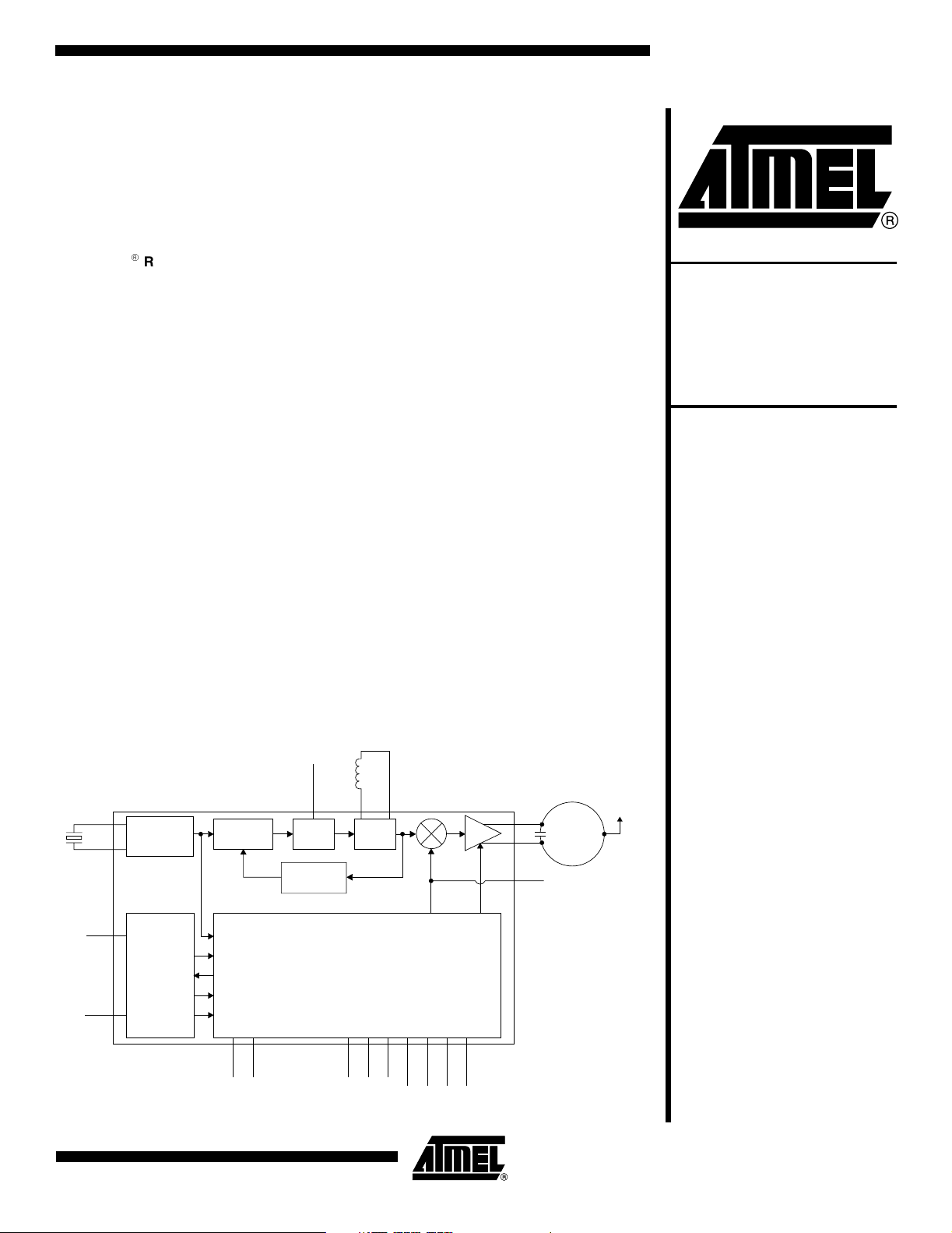
Figure 1. Block Diagram
XTAL/CLK
XTALB
OSCILLATOR
PHASE
DETECTOR
RISC microcontroller. It requires only a crystal, a
L1
VCO
L2
ANT
RF
AMP
ANTB
CFIL
LOOP FIL
LOOP
FILTER
PRESCALER
÷
24
B+
AT86RF401
Preliminary
AVDD
AGND
POWER
SUPPLY
SUPERVISOR
CLOCK
RESET
WATCHDOG
LOW-VOLTAGE DETECT
BROWN-OUT PROTECT
DVDD
DGND
DATA
AVR RISC µC
2 KB Flash Program Memory
128 Bytes EEPROM Data Memory
IO5
IO4
IO3
SDI/IO0
SCK/IO2
SDO/IO1
GAIN
TRIM
RESETB
1424D–RKE–09/02
1
Page 2

In-system programmable, nonvolatile Flash program memory and EEPROM data storage make possible rapid time-to-market and lower inventory costs.
Static current consumption is kept to a minimum with an ultra-low current shutdown
mode. Normal operation resumes when a button is pressed. This activates the crystal
oscillator circuit that serves as the clock for the AVR microcontroller.
The RF carrier is synthesized utilizing an on-board Voltage Controlled Oscillator (VCO).
Optimal tuning of the VCO is maintained over component tolerance through the use of a
software-controlled switched capacitor array. Its accuracy is maintained with a PLL
detector that compares the crystal oscillator to a frequency-scaled version (divided by
24) of the RF carrier. The resulting error signal adjusts the VCO to produce a very stable
RF carrier.
An interrupt-based bit-timer structure, integral to the AVR microcontroller, simplifies the
implementation of user-specific, data-bit encoding routines, such as PWM or Manchester, for modulating the RF carrier. Thirty-six dB of RF power output control is available to
the user in 1 dB steps and is addressable in software. The RF signal output is placed
differentially on a tuned-loop antenna, which may be realized as a counterspread copper trace on a PCB.
The AT86RF401 is fabricated in Atmel’s 0.6 µm Mixed Signal CMOS + EEPROM process, enabling true system-level integration (SLI).
Figure 2. 20-lead TSSOP
ANTB
LOOPFIL
RESETB
N/C
I/O0 (SDI)
I/O1 (SDO)
I/O2 (SCK)
XTAL/CLK
L1
L2
1
2
3
4
5
6
7
8
9
10
20
19
18
17
16
15
14
13
12
11
ANT
CFIL
AVDD
DVDD
AGND
DGND
I/O5
I/O4
I/O3
XTALB
2
AT86RF401
1424D–RKE–09/02
Page 3
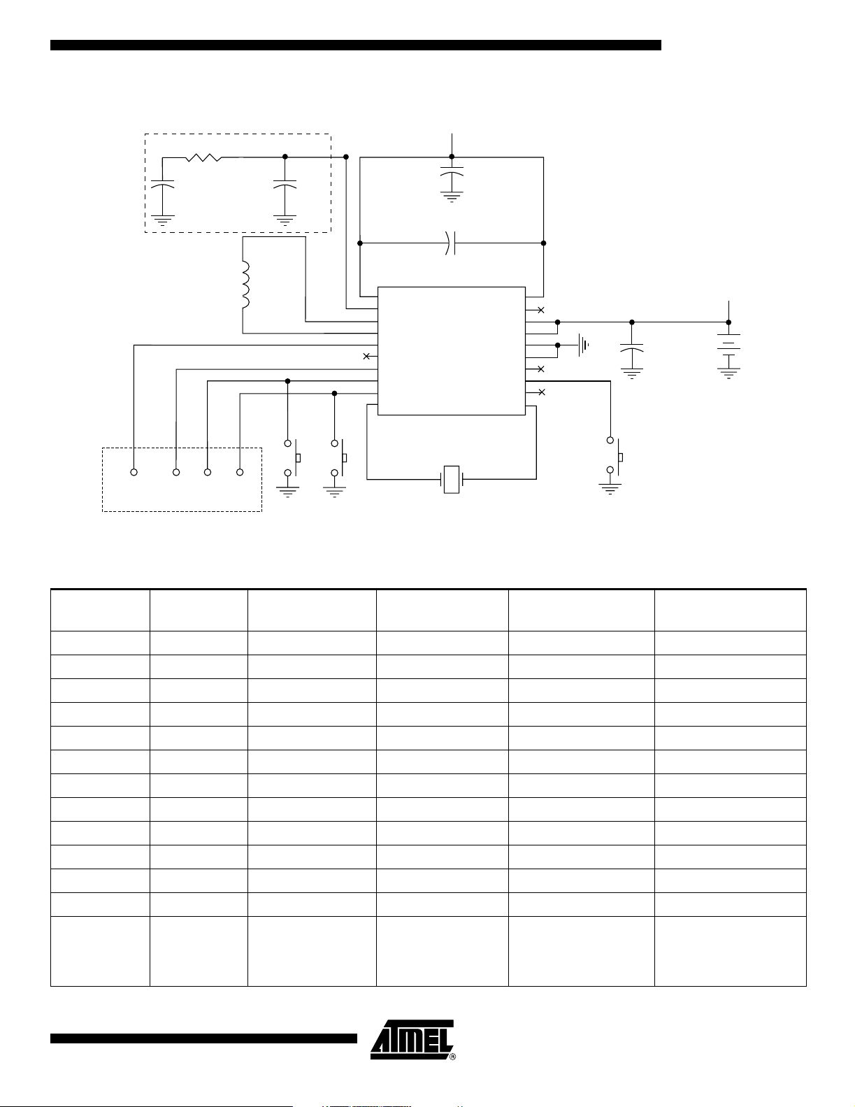
Figure 3. Sample Circuit
EXTERNAL LOOP FILTER (OPTIONAL)
AT86RF401
V+
R1
C4
L1
RESET SDO
SDI
SCLK
SPI Programming Interface
S1
C3
U1
Y1
C2
ANT
CFIL
AVDD
DVDD
AGND
DGND
IO5
IO4
IO3
XTALB
20
19
18
17
16
15
14
13
12
11
C5
1
ANTB
2
LOOPFIL
3
L1
4
L2
5
RESETB
6
NC
7
IO0/SDI
8
IO1/SDO
9
IO2/SCLK
10
XTAL/CLK
S2 S
V+
C1 B1
3
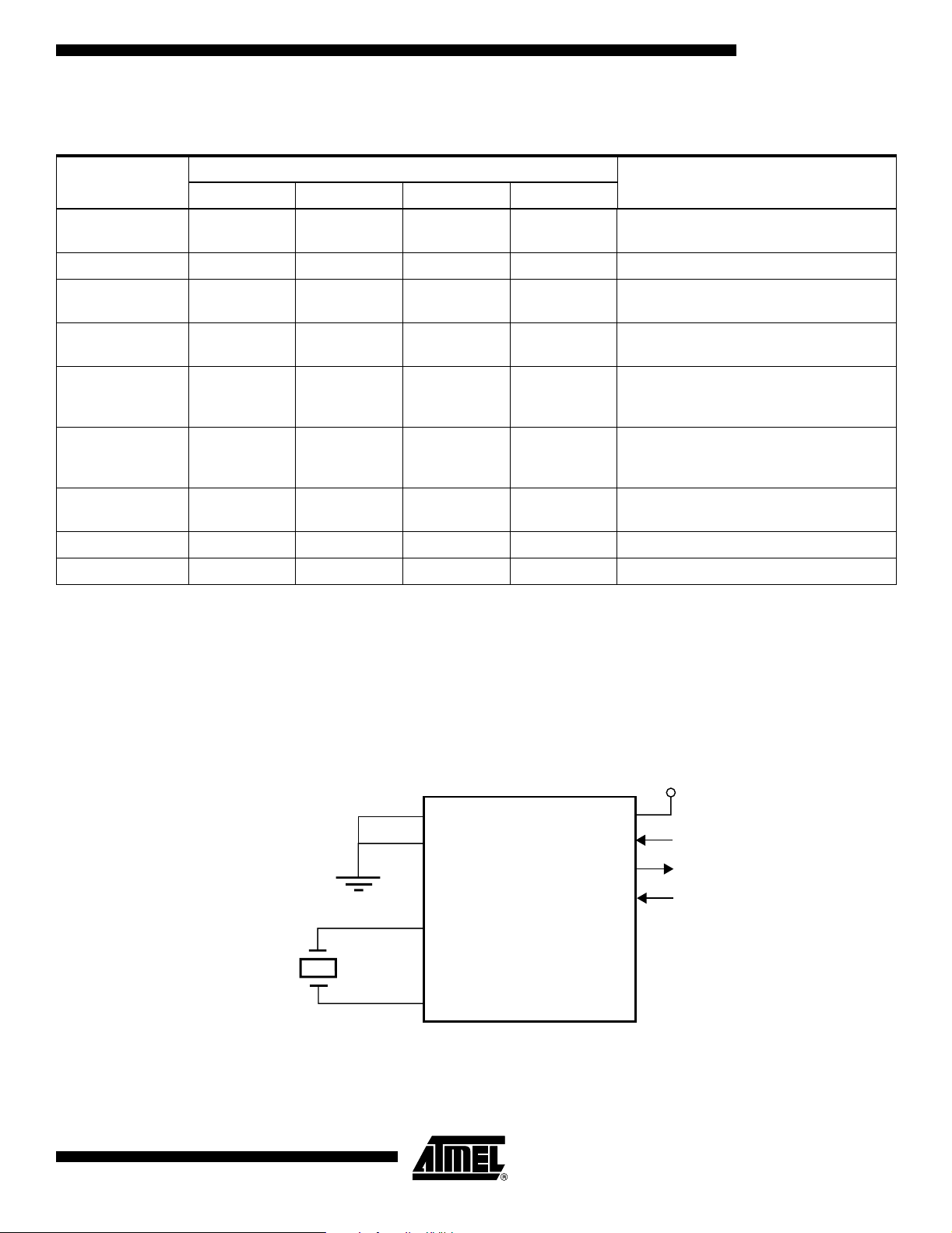
Table 1. Recommended Parts List
Value
Part Number
B1 3.6V CR2032, Li Battery
C1 0.01 µF 0603, X7R, ± 10%
C2 100 pF 0603, COG, ± 5%
C3 Antenna Dependent Antenna Dependent Antenna Dependent 0603, COG, ± 0.1 pF
C4 Not req’d Not req’d Frequency Dependent 0603, COG, ± 5%
C5 Not req’d Not req’d Frequency Dependent 0603, COG, ± 0.25 pF
L1 82 nH 39 nH Frequency Dependent 1608, ± 5%
R1 Not req’d Not req’d Frequency Dependent 0603, ± 5%
S1 Switch SPST
S2 Switch SPST
S3 Switch SPST
U1 AT86RF401 20-lead TSSOP
Y1 13.125 MHz 18.08 MHz Frequency Dependent
(Common)
Value
(315 MHz)
Value
(433.92 MHz)
Value
(Ext. Loop Filter) Specification
13.125 MHz:
Crystek
™
P/N 016757
18.080 MHz:
Crystek P/N 016758
1424D–RKE–09/02
3
Page 4
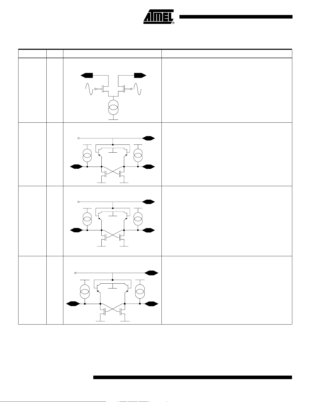
Table 2. Pin Descriptions – 20-lead TSSOP
Symbol Pin Description
120
ANTB 1 Differential Antenna Output
10 mA
LOOPFIL 2
L1 3
V
VCO
V
DD
2
V
DD
External VCO Loop-filter Connection.
V
is the VCO control voltage.
3
V
VCO
V
DD
4
2
V
DD
VCO
External VCO Inductor Connection.
V
is the VCO control voltage.
3
V
VDD
V
DD
4
2
V
DD
VCO
L2 4
4
AT86RF401
External VCO Inductor Connection.
V
is the VCO control voltage.
3
4
VCO
1424D–RKE–09/02
Page 5
Table 2. Pin Descriptions – 20-lead TSSOP (Continued)
V
DD
AT86RF401
SPI Reset Input: A “low” on this pin resets the device and puts
the part into SPI mode. A logic-high on this pin causes the
device to execute its program if the V
RESETB 5
35 k Ω
5
out voltage level.
To AV R
NC 6 No Connect. Float Pin.
V
DDVDD
I/O0 (SDI) 7
I/O1 (SDO)
Data
nable−
Data
Enable
V
DD
Data
Enable−
8
Data
Enable
35 k Ω
7
SPI Data In/Input/Output 0: General-purpose I/O and button
input. In SPI mode, this pin serves as SDI (Serial Data Input).
To AV R
V
DD
35 k Ω
SPI Data Out/Input/Output 1: General-purpose I/O and button
8
input. In SPI mode, this pin serves as SDO (Serial Data
Output).
To AV R
is above the brown-
DD
I/O2 (SCK)
XTAL/CLK 10
1424D–RKE–09/02
V
V
DD
DD
Data
Enable−
9
Data
Enable
10
40 pF
35 k Ω
9
To AV R
SPI Clock/Input/Output 2: General-purpose I/O and button
input. In SPI mode, this pin serves as SCK (SPI Clock Input).
Crystal/Clock Input: Input to the inverting oscillator amplifier
and input to the internal clock operating circuit. This pin may
be driven externally for test purposes.
11
40 pF
5
Page 6
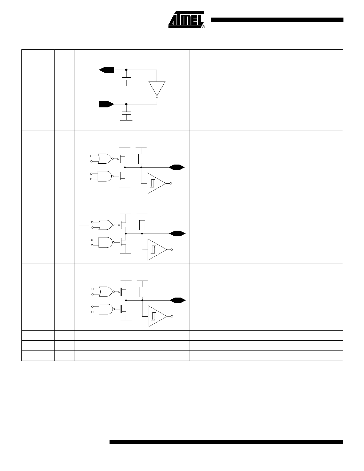
Table 2. Pin Descriptions – 20-lead TSSOP (Continued)
10
40 pF
XTALB 11 Crystal Output: Output from the inverting oscillator amplifier
11
40 pF
V
V
DD
DD
Data
IO3 12 Input/Output 3: General-purpose I/O and button input
IO4 13 Input/Output 4: General-purpose I/O and button input
Enable
Data
Enable
Data
Enable
Data
Enable
V
DD
35 k Ω
V
DD
35 k Ω
12
To AV R
13
To AV R
V
V
DD
DD
Data
IO5 14 Input/Output 5: General-purpose I/O and button input
Enable
Data
Enable
35 k Ω
14
To AV R
DGND 15 Digital Ground
AGND 16 Analog Ground
DVDD 17 Digital Voltage Supply
6
AT86RF401
1424D–RKE–09/02
Page 7
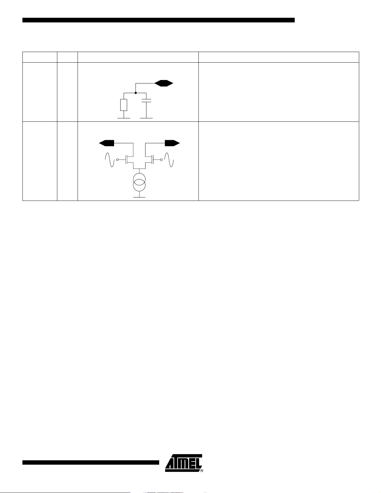
Table 2. Pin Descriptions – 20-lead TSSOP (Continued)
AVDD 18 Analog Voltage Supply
19
CFIL 19 External Data Rate Filter
420 KΩ
120
ANT 20 Differential Antenna Output
1.06 pF
10 mA
AT86RF401
1424D–RKE–09/02
7
Page 8

Absolute Maximum Ratings*
Antenna Voltage (Pins 1, 20)...................................... −1V to 10V
Operating Temperature ........................................−40°Cto+85°C
Storage Temperature (without bias) ................−55°Cto+125°C
Voltage on V
Voltage on Pins 2–19 (TSSOP 20) ................ −0.1 to V
with respect to ground ............................. 6.0V
DD
DD
+0.3V
*NOTICE: Stresses beyond those listed under “Absolute
Maximum Ratings” may cause permanent damage to the device. This is a stress rating only;
functional operation of the device at these or
other conditions beyond those indicated in the
operational sections of this specification is not
implied. Exposure to absolute maximum rating
conditions for extended periods may affect device
reliability.
DC Characteristics
VDD=3.3V;f
Symbol Parameter Conditions Min Typ Max Unit
Supply
V
DD
I
DD
= 13.125 MHz; f
XTAL
AVR=fXTAL
÷ 16; TA=25°C unless otherwise specified.
Supply Voltage 2.0 3.3 5.0 V
=3.3V
V
Standby Current (off)
DD
= 25°C
T
A
– 0.1 0.5 µA
AVR Active – 3.4 – mA
Frequency Synthesizer + AVR Active – 14.3 – mA
Transmit (FS, AVR and Power Amp active) CW modulation – 23.2 – mA
Digital Inputs (SDI, SCK, RESETB, IOx)
V
IH
V
IL
I
IH
I
IL
High-level Input Voltage 0.8* V
Low-level Input Voltage 0 – 0.2* V
High-level Input Current VIH=V
Low-level Input Current VIL=0V, VDD=5.0V −140 ––µA
Digital Outputs (SDO, IOx)
V
OH
V
OL
High-level Output Voltage IOH= −500 µA VDD−0.4 ––V
Low-level Output Voltage IOL=2mA ––0.4 V
Microcontroller/System
t
TX
f
AVR
EE
EE
LIFE
CYCLES
Time from Button Wake-up to RF Outputs Active – 0.5 1.0 ms
AVR Clock Frequency ––1.25 MHz
EEPROM Retention
EEPROM Write/Erase Endurance
, V
DD
=5.0V ––1µA
DD
Initial programming
conditions:
V
=3.3V±10%
DD
Te mp = 25 °C±10%
2.0V ≤ V
DD
≤ 5.0V
−40°C ≤ Te m p ≤
85°C
DD
– V
DD
DD
V
V
––10 years
––100,000 cycles
8
AT86RF401
1424D–RKE–09/02
Page 9
Analog/RF Specs
AT86RF401
VDD=3.3V;f
Symbol Parameter Conditions Min Typ Max Unit
RF Amplifier
I
PA
P
CTLRANGE
P
CTLRES
Crystal Oscillator
f
OSC
Frequency Synthesizer/PLL
F
OUT
1
P
HARM
f
MOD
Note: 1. Characterized but not guaranteed by test due to dependency on PCB trace antenna
Functional
= 13.125 MHz; f
XTAL
Power Amp Output Current Transmitting (RF “ON”), 0 dB Attenuation – 8.6 – mA
Power Control Range – 36 – dB
Power Control Resolution – 1 – dB
Oscillation Frequency Range 11 – 19 MHz
Output Frequency Range 264 – 456 MHz
Harmonics
OOK Modulation Data Rate Using Manchester Data Bit Encoding ––10 Kbps
AVR=fXTAL
÷ 16; TA=25°C unless otherwise specified.
I/O Pins Static during RF Transmission
Using PCB Trace Antenna
– −60 – dBc
The complete circuit consists of the following functional blocks.
Description
Transmitter
Crystal Oscillator The crystal oscillator circuit is designed to work with crystals with fundamental frequen-
cies between 11 and 19 MHz. Forty pF of internal capacitance is connected between
each of the crystal input pins and (chip) ground. Alternatively, an external clock can be
used for these functions.
This circuit provides the master clock for the entire chip. A programmable divider is used
to provide the AVR system clock.
Radio Frequency Power Amplifier
Frequency Synthesizer The frequency synthesizer utilizes a PLL, which consists of a phase detector, a ÷24
Lock Detector The lock detection block provides an indication of the state of the phase lock loop (PLL).
The RF power amplifier generates a differential output suitable for driving an off-chip
tuned-loop antenna from the PLL output. The PLL output signal is gated using on-off
keyed (OOK) modulation before transmission. It is used as the RF carrier frequency for
the transmitted data stream. The amplifier can be configured via software to reduce the
power output by 36 dB (with 1 dB resolution).
prescaler, an on-chip loop filter and an integrated VCO. The VCO output is buffered
prior to the output amplifier. The output frequency is 24 times the crystal frequency. To
offset component tolerance, a switched capacitor array is connected between pins 3
and 4 of the VCO. Thirty-two discrete steps of capacitance are available to tune the
VCO control voltage. An internal window comparator monitors the magnitude of the tuning voltage and is used by the AVR core to determine the optimal tuning configuration.
Lock condition is determined by counting the number of cycle slips in a given time
1424D–RKE–09/02
9
Page 10
period. A number of registers are available to adjust the performance of the lock detector. These include lock delay and unlock delay timers as well as a cycle slip counter.
Bandgap Reference The device uses a 1.2V (nominal) bandgap reference generator to provide consistent
performance over a wide range of input supply voltages. This reference voltage is used
throughout the device.
Brown-out Protection/Low Battery Detection
Brown-out Protection
Low Battery Detection
The brown-out protection and low battery detection functions consist of a voltage reference, a sampling block and an autozero comparator. The circuit’s primary operating
mode is brown-out protection.
The brown-out protection circuit detects when the level of VDDdrops below the minimum
voltage that guarantees proper operation. The brown-out voltage for this device is typically 1.8 volts.
If a brown-out occurs, the device enters a reset state. It stays in this state until either of
the following occurs:
• The level of VDDincreases ~0.1–0.2 volts above the brown-out voltage. This causes
the device to enter a warm reboot state.
• The level of V
drops to ~0 volts, then increases above the POR level. This places
DD
thedeviceintothe“cold start” mode of operation, identical to battery insertion.
The low battery detection feature allows the programmer to select a value for VDDat
which a warning is issued to the user. This warning may be utilized to activate an I/O
port, for example.
If low battery detection occurs, Bit 7 of register BL_CONFIG is set. Bit 6 of register
BL_CONFIG is used to indicate that Bit 7 is valid. It is left to the programmer to poll both
bits to ensure the potential warning is valid.
Bits 5–0 of register BL_CONFIG are used to program the low battery detect level. This
warning level is programmable between ~1.5–2.7 volts.
Note: The warning level can be set below the brown-out voltage level.
The formula for calculating the low battery detection threshold is located in Table 3.
Table 3. Low Battery Detection Threshold Formulas (V
VDDFalling
VDD
-----------------------------------------------------------=
1
3.887 V
0.887
---------------
BL[5:0] 71 3.887
10
AT86RF401
63
×
REF
× BL[5:0]+
V
REF
-------------
V
1–××=
DD
bo_hyst = 1 (large hysteresis) bo_hyst = 0 (small hysteresis)
VDD
BL[5:0] 71 4.05
is approximately 0.7 volts)
REF
4.05 V
×
× BL[5:0]+
REF
V
REF
-------------
V
DD
-----------------------------------------------------------=
0.887
---------------
1
63
1–××=
V
Rising
DD
VDD
BL[5:0] 71 4.22
-----------------------------------------------------------=
1
4.22 V
×
0.887
---------------
63
REF
× BL[5:0]+
V
REF
-------------
V
DD
1424D–RKE–09/02
1–××=
Page 11

AT86RF401
Bit Timer A hardware assist has been included in the AT 86 R F4 01 to make transmission of data
easier. Keying of the transmitter is timed by this logic, and interrupts are generated
when data is needed by the timer or when transmission is complete. The timer also supports code that uses polling instead of interrupts. Using polling instead of interrupts may
facilitate higher bit rates. Additionally, this timer may be used to time pulses arriving at
the I/O3 pin. This enables the AT86RF401 to be used to decode the signal detected by
an external receiver chip.
Transmit Mode Bit Coding and Timing
Interrupts There are two interrupts associated with transmit mode:
Bit Timer in Receive Mode When put into receive mode, the bit timer times pulses arriving at the I/O3 pin. When
Bit coding is done by the AVR before data is sent to the bit timer. Bit timing is controlled
by the count value in the Bit Timer Count (BTCNT) register and the two most significant
bits in the Bit Timer Control Register (BTCR). Generally the time of each bit is:
P
P countval 1+()×=
xx
where
P
istheperiodofeachtimeslotand
and BTCR registers.
countval
1. Transmit Buffer Empty Interrupt: This vectors to address 0x04. Flag 0 is set, and,
2. TXDONE Interrupt: This vectors to address 0x02. Flag 2 is set, and, if enabled,
enabled, the counter counts up from zero and places that value in the BTCNT register
when an edge occurs. If the edge is rising, the DATA bit in the BTCR is set. If the edge
is falling, the DATA bit in the BTCR is reset. This mode may be used to decode signals
from a receiver chip easily.
xx
= {BTCR[7:6], BTCNT[7:0]}.
if enabled, this interrupt is generated when the timer removes the value from the
DATA bit in the BTCR. This interrupt service routine should load the next bit into
the DATA bit in the BTCR.
an interrupt is generated when the counter has counted down to zero and the
buffer is empty. This indicates that the transmission is complete. This interrupt
service routine should turn off the transmitter and turn off the bit timer using the
mode bits.
P
is the AVR clock period that is set in the PWR_CTL register.
countval
is the counter value in the BTCNT
Bit Timer Operation as a Generic Timer/Counter
1424D–RKE–09/02
The Bit Timer may be used as a generic timer by not allowing it to key off the transmitter.
An interrupt is generated after the amount of time dictated by the count value.
11
Page 12

Watchdog Timer When enabling the watchdog timer, the status of the watchdog time is unknown. The
user is advised to execute a WDR instruction before enabling the watchdog. Otherwise,
the device might get reset before the first WDR after enabling is reached. To prevent the
unintentional disabling of the watchdog, a special turn-off procedure must be followed
when the watchdog is disabled. Refer to the description of the Watchdog Timer Control
Register on page 38 for details (see Register $22 in I/O Memory). The watchdog timer
prescaler determines the number of system clocks that occur before the watchdog reset
is asserted. The system clock is determined by Bits[7:5] of the AVR_CONFIG register.
Reset and Interrupt Handling
The AT86RF401 Reset and Interrupt vectors are defined in Table 4. The I-bit in the status register must be set to enable the interrupts.
Table 4. Reset and Interrupt Vectors
Vector
Number
1 $000 RESETB, Watchdog, Buttons Hardware Pin or Watchdog or
2 $002 Transmission Done (TXDONE) Bit Timer Flag 2 Interrupt
4 $004 Transmit Buffer Empty Bit Timer Flag 0 Interrupt
Program
Address Source Interrupt Definition
The most typical and general program setup for the Reset and Interrupt Vector
Addresses are:
Address Labels Code Comments
$000 jmp RESET ; Reset handler
$002 jmp BT_F2_ISR ; Bit timer flag 2 interrupt service routine
$004 jmp BT_F0_ISR ; Bit timer flag 0 interrupt service routine
$006 MAIN: <instr> xxx ; Main program start
…… ……
Reset Sources The AT86RF401 has several sources of reset:
• Power-on Reset: The device is reset when the supply voltage is applied between the
VDD and GND pins. There are 10
occurring and the part becoming active. This is to ensure that the power is stable.
• External Reset: The device is reset when a logic low level is present on the RESETB
pin. This resets all I/O Registers and puts the part into SPI mode. The I/O Registers
may be read and written by the SPI interface after two AVR System Clocks.
• Watchdog Reset: This is similar to power-on reset but is caused by the watchdog
timer and does not have a 10
• Brown-out Reset: This is caused by the battery voltage dropping below the Brownout Threshold voltage trip point.
• Button Reset (software reset): The part is placed into a special reset state by
software. The part is released from reset when a properly configured button is
activated, and the part is not in external reset or brown-out reset. In the button reset
state, most I/O registers are not reset.
6
cycles of delay between Power-on Reset
6
cycle delay prior to becoming active.
Button Reset
12
AT86RF401
1424D–RKE–09/02
Page 13

AT86RF401
During power-on reset and watchdog reset, all I/O registers are set to their initial values,
and the program starts execution from address $000.
Note: The instruction placed in address $000 must be an RJMP (relative jump) instruction or a
JMP (absolute jump) to the reset handling routine. If an RJMP or JMP instruction is not
present at address $000, the part is placed into a “no program” resetstate.Thisistopro-
tect the part from fetching instructions when no program is present.
Interrupt Response Time The interrupt execution response for all the enabled AVR interrupts is a minimum of four
clock cycles. After the four clock cycles, the program vector address for the actual interrupt handling routine is executed. During this four clock cycle period, the Program
Counter is pushed onto the stack. The vector is a jump to the interrupt routine, and this
jump takes two clock cycles. If an interrupt occurs during execution of a multi-cycle
instruction, this instruction is completed before the interrupt is served.
A return from an interrupt handling routine takes four clock cycles. During these four
clock cycles, the Program Counter is popped back from the stack. When AVR exits from
an interrupt, it will always return to the main program and execute one more instruction
before any pending interrupt is served.
Note: The Status Register (SREG) is not saved by the AVR hardware. This must be performed
by user software when required.
Memory Programming
Program Memory Lock Bits
In-system Flash and EEPROM
SPI Interface Both the program and data memory arrays can be programmed using the serial SPI bus
The AT86RF401 microtransmitter provides two lock bits that can be left unprogrammed
(“1”) or can be programmed (“0”) to obtain the additional features listed in Table 5.
Table 5. Lock Bit Protection Modes
Program Lock Bits
ModeLB1 LB2
Protection Type
1 1 1 No program lock features
201
3 0 0 Same as mode 2, but Verify is also disabled
Note: The lock bits can only be erased with the Chip Erase operation.
The AT86RF401 offers 2 Kbytes (1K x 16) of in-system reprogrammable Flash program
memory and 128 bytes of EEPROM data memory. This memory can be programmed
serially via the SPI interface.
while RESETB is pulled to GND. The serial interface consists of pins SCK, SDI (input)
and SDO (output).
Further programming of the EEPROM is disabled (both program and
data memory).
1424D–RKE–09/02
When programming, an auto-erase cycle is built into the self-timed programming operation, and there is no need to first execute the Chip Erase instruction. The Chip Erase
operation sets every memory location in the EEPROM array to $FF.
Either an external system clock is supplied at pin XTAL/CLK or a crystal needs to be
connected across pins XTAL/CLK and XTALB. The minimum low and high periods for
the serial clock (SCK) input are defined as follows:
Low:
4 XTAL Clock Cycles
High:
16 XTAL Clock Cycles
13
Page 14

Serial Programming Algorithm
Refer to Figure 4 (page 15), Figure 5 (page 16) and Figure 6 (page 17). To program and
verify the AT86RF401 in the serial programming mode, the following sequence is
recommended.
Power-up Sequence:
1. Apply power between VDD and GND while RESETB and SCK are set to “0”.Ifa
crystal is not connected across pins XTAL and XTALB, apply a clock signal to the
XTAL pin. If the programmer can not guarantee that SCK is held low during
power-up, RESETB must be given a positive pulse after SCK has been set to “0”.
2. Wait for at least 20 ms and enable serial programming by sending the Programming Enable instruction to pin SDI. This must occur prior to any program/erase
operations.
3. If a chip erase is performed, wait 4 ms, give RESETB a positive pulse and start
over again from Step 2.
4. The array is programmed one byte at a time by supplying the address and data
together with the appropriate Write instruction. The memory location is first automatically erased before new data is written. The next byte can be written after
4ms.
5. Any memory location can be verified by using the Read instruction, which
returns the content at the selected address at serial output SDO.
6. At the end of the programming session, RESETB must be set high to commence
normal operation.
14
AT86RF401
1424D–RKE–09/02
Page 15
Data EEPROM Access from the AVR
Table 6. AT86RF401 Serial Programming Instruction Set
Instruction Format
AT86RF401
Instruction
Programming
Enable
Chip Erase
Read Program
Memory
Write Program
Memory
1010 1100 0101 0011 xxxx xxxx xxxx xxxx
1010 1100 100x xxxx xxxx xxxx xxxx xxxx
0010 H000 0000 00aa bbbb bbbb oooo oooo
0100 H000 0000 00aa bbbb bbbb iiii iiii
Read
EEPROM
1010 0000 0000 0000 xbbb bbbb oooo oooo
Memory
Write
EEPROM
1100 0000 0000 0000 xbbb bbbb iiii iiii
Memory
Write Lock Bits
I/O Read
I/O Write
1010 1100 111x x21x xxxx xxxx xxxx xxxx
10110000 0000 0000 00bbbbbb oooo oooo
11010000 0000 0000 00bbbbbb iiii iiii
Note: a = address high bits
b = address low bits
H =0:Lowbyte,1:Highbyte
o = data out
i = data in
x = don’tcare
1=lockbit1
2=lockbit2
OperationByte 1 Byte 2 Byte 3 Byte 4
Enable Serial Programming after
RESETB goes low.
Chip erase EEPROM
Read H (high or low) data o from Program
memory at word address a:b
Write H (highorlow)datai to Program
memory at word address a:b
Read data o from EEPROM memory at
address b
Write data i to EEPROM memory at
address b
Write lock bits. Set bits 21 = “0” to
program lock bits.
Read data 0 from I/O memory address b
Write data i to I/O memory address b
1424D–RKE–09/02
Figure 4. Serial Programming and Verify
AT86RF401
RESETB
GND
6 to 20 MHz
Notes: 1. When
2. When
explanation.
XTALB
XTAL
writing
,dataisclockedonthe
reading
, data is clocked on the
BAT
SCK
SDO
SDI
rising
falling
2.0–3.5V
CLOCK IN
DATA OUT
INSTR. IN, DATA IN
edge of CLK.
edge of CLK. See Figure 5 for an
15
Page 16

Figure 5. Serial Programming Waveforms
SERIAL DATA INPUT (SDI)
SERIAL DATA OUTPUT (SDO)
SERIAL CLOCK INPUT (SCK)
Note: This device includes an integrated 128-byte EEPROM, which is accessed by three registers located in the I/O memory space.
These are the DEECR, DEEDR and DEEAR registers. For more information, refer to I/O Register Description.
MSB
MSB LSB
LSB
AVR Core
Architectural Overview The fast-access register file concept contains 32 x 8-bit general-purpose working regis-
ters with a single clock cycle access time. This means that during one single clock cycle,
one Arithmetic Logic Unit (ALU) operation is executed. Two operands are output from
the register file, the operation is executed, and the result is stored back in the register
file in one clock cycle.
Six of the 32 registers can be used as three 16-bit indirect address register pointers for
Data Space addressing, enabling efficient address calculations. One of the three
address pointers is also used as the address pointer for look-up tables in Flash program
memory. These added function registers are the 16-bit X-register, Y-register and Zregister.
The ALU supports arithmetic and logic operations between registers or between a constant and a register. Single register operations are also executed in the ALU. Figure 6
shows the AT86RF401 AVR architecture.
In addition to the register operation, the conventional memory addressing modes can be
used on the register file as well. This is enabled by the fact that the register file is
assigned the 32 lowest data space addresses ($00–$1F), allowing them to be accessed
as though they were ordinary memory locations.
The I/O memory space contains 64 addresses for CPU peripheral functions as Control
Registers, Timer/Counters, A/D converters and other I/O functions. The I/O Memory can
be accessed directly or as the Data Space locations following those of the register file,
$20–$5F.
16
AT86RF401
1424D–RKE–09/02
Page 17
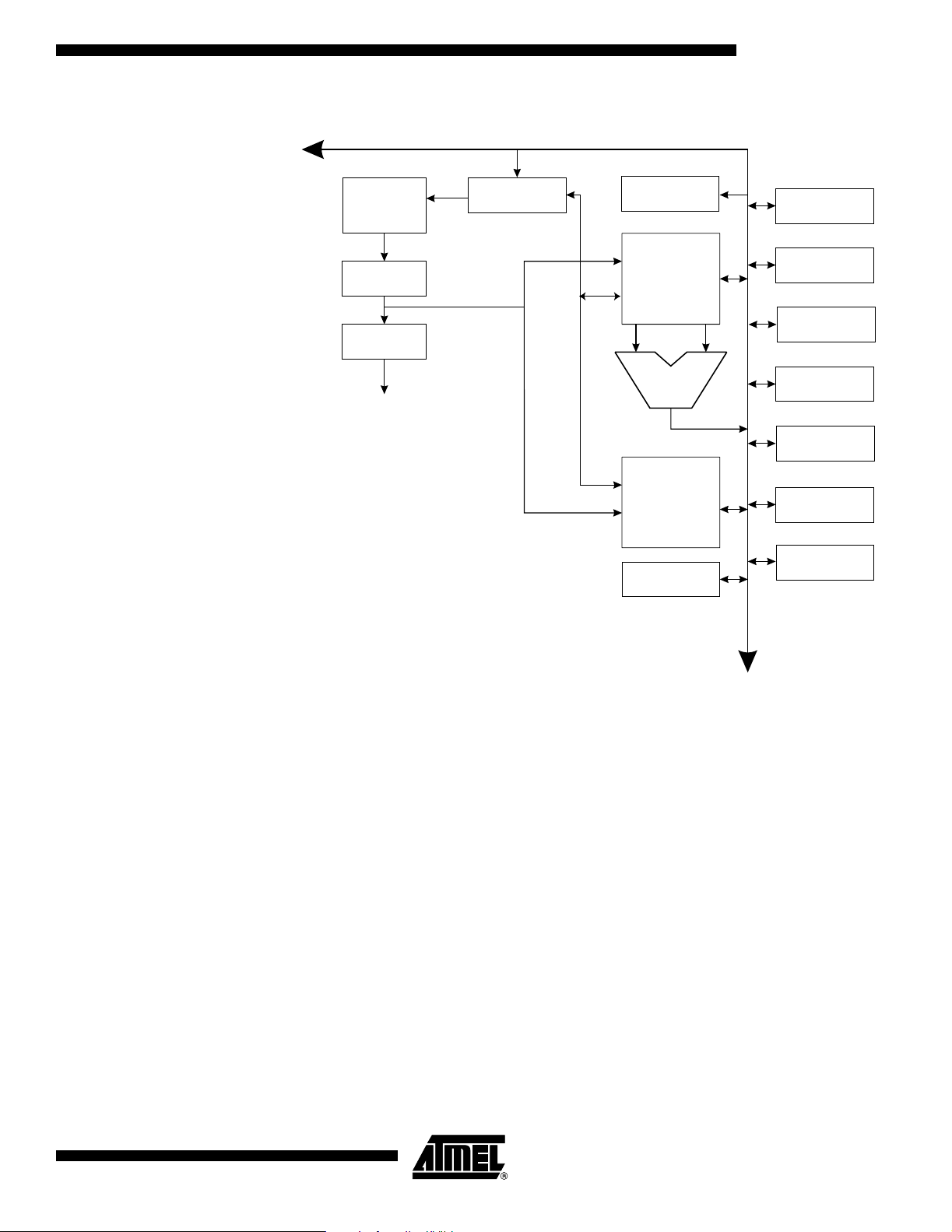
Figure 6. AVR Core Architecture
AT86RF401
Data Bus 8-bit
1K x 16
Program
Memory
Instruction
Register
Instruction
Decoder
Control Lines
Program
Counter
Direct Addressing
Status
and Control
32 x 8
General
Purpose
Registers
ALU
Indirect Addressing
128 x 8
Data
SRAM
128 x 8
EEPROM
Bit Timer
SPI Unit
RF
Transmitter
Brown-out/Low
Battery Detector
Programmable
Clock Divider
6
I/O Lines
Watchdog
Timer
The AVR uses a Harvard architecture concept, with separate memories and buses for
program and data. The program memory is executed with a two-stage pipeline. While
one instruction is being executed, the next instruction is prefetched from the program
memory. This concept enables instructions to be executed in every clock cycle. The program memory is in-system, reprogrammable Flash memory.
With the jump and call instructions, the whole 1K word address space is directly
accessed. Most AVR instructions have a single 16-bit word format. Every program
memory address contains a 16- or 32-bit instruction.
During interrupts and subroutine calls, the return address program counter (PC) is
stored on the stack. The stack is effectively allocated in the general data SRAM, and
consequently the stack size is only limited by the total SRAM size and the usage of the
SRAM. All user programs must initialize the SP in the reset routine (before subroutines
or interrupts are executed). The 7-bit stack pointer SP is read/write accessible in the I/O
space.
The 128-byte data SRAM can be easily accessed through the five different addressing
modes supported in the AVR architecture.
The memory spaces in the AVR architecture are all linear and regular memory maps.
1424D–RKE–09/02
17
Page 18

A flexible interrupt module has its control registers in the I/O space with an additional
global interrupt enable bit in the status register. All interrupts have a separate interrupt
vector in the interrupt vector table at the beginning of the program memory. The interrupts have priority in accordance with their interrupt vector position; the lower the
interrupt vector address, the higher the priority.
Figure 7. Memory Maps
Program Memory
$000
Application Flash Section
$3FF
18
AT86RF401
1424D–RKE–09/02
Page 19

AT86RF401
General-purpose Register File
Figure 8 shows the structure of the 32 general-purpose working registers in the CPU.
Figure 8. AVR CPU General-purpose Working Registers
70Addr.
R0 $00
R1 $01
R2 $02
…
R13 $0D
R14 $0E
R15 $0F
R16 $10
R17 $11
…
R26 $1A X-register low byte
R27 $1B X-register high byte
R28 $1C Y-register low byte
R29 $1D Y-register high byte
R30 $1E Z-register low byte
R31 $1F Z-register high byte
All the register operating instructions in the instruction set have direct and single cycle
access to all registers. The only exception is the five constant arithmetic and logic
instructions (SBCI, SUBI, CPI, ANDI and ORI) between a constant and a register, and
the LDI instruction for load immediate constant data. These instructions apply to the
second half of the registers in the register file, R16...R31. The general SBC, SUB, CP,
AND and OR and all other operations between two registers or on a single register apply
to the entire register file.
As shown in Figure 9, each register is also assigned a data memory address, mapping
the registers directly into the first 32 locations of the user data space. Although not being
physically implemented as SRAM locations, this memory organization provides great
flexibility in access of the registers, as the X, Y and Z registers can be set to index any
register in the file.
1424D–RKE–09/02
19
Page 20

TheX,YandZRegisters The registers R26...R31 have some added functions to their general-purpose usage.
These registers are address pointers for indirect addressing of the data space. The
three indirect address registers X, Y and Z are defined as shown in Figure 9.
Figure 9. The X, Y and Z Registers
15 XH XL 0
XRegister 70 0 7 0
R27 ($1B) R26 ($1A)
15 YH YL 0
YRegister 70070
R29 ($1D) R28 ($1C)
15 ZH ZL 0
ZRegister 70 0 7 0
R30 ($1F) R31 ($1E)
In the different addressing modes, these address registers have functions as fixed displacement, automatic increment and decrement (see the descriptions for the different
instructions).
Arithmetic Logic Unit (ALU)
In-system Selfprogrammable Flash
Program Memory
The high-performance AVR ALU operates in direct connection with all the 32 generalpurpose working registers. Within a single clock cycle, ALU operations between registers in the register file are executed. The ALU operations are divided into three main
categories: arithmetic, logical and bit-functions. The multiplier is not present in this version of the core. Therefore, the MUL instruction is not supported.
The AT86RF401 contains 2 Kbytes of on-chip Flash memory for program storage. Since
all instructions are 16- or 32-bit words, the Flash is organized as 1K x 16.
The Flash memory has an endurance of at least 1000 write/erase cycles. The PC is 10
bits wide, thus addressing the 1024 program memory locations. See the Memory Programming section (page 13) for a detailed description on Flash data serial downloading.
Constant tables can be allocated within the entire program memory address space (see
Table 10, Instruction Set, page 44).
20
AT86RF401
1424D–RKE–09/02
Page 21

AT86RF401
SRAM Data Memory Figure 10 shows how the AT86RF401 SRAM memory is organized.
Figure 10. SRAM Organization
Register File
R0
R1
R2
...
R29
R30
R31
I/O Registers
$00
$01
$02
...
$3D
$3E
$3F
Data Address Space
$0000
$0001
$0002
...
$001D
$001E
$001F
$0020
$0021
$0022
...
$005D
$005E
$005F
Internal SRAM
$0060
$0061
...
$00DE
$00DF
Program and Data Addressing Modes
The lower 224 Data Memory locations address the Register File, the I/O Memory and
the internal data SRAM. The first 96 locations address the Register File + I/O Memory,
and the next 128 locations address the internal data SRAM.
The five different addressing modes for the data memory cover: Direct, Indirect with Displacement, Indirect, Indirect with Pre-decrement, and Indirect with Post-increment. In
the register file, registers R26 to R31 feature the indirect addressing pointer registers.
The direct addressing reaches the entire data space.
The Indirect with Displacement mode features a 63 address locations reach from the
base address given by the Y or Z register.
When using register indirect addressing modes with automatic pre-decrement and postincrement, the address registers X, Y and Z are decremented and incremented.
The 32 general-purpose working registers, 64 I/O registers and the 128 bytes of internal
data SRAM in the AT86RF401 are all accessible through all these addressing modes.
The AT86RF401 AVR Enhanced RISC microcontroller supports powerful and efficient
addressing modes for access to the program memory (Flash) and data memory (SRAM,
Register File and I/O Memory). This section describes the different addressing modes
supported by the AVR architecture. In the figures, OP means the operation code part of
the instruction word. To simplify, not all figures show the exact location of the addressing bits.
1424D–RKE–09/02
21
Page 22

Register Direct, Single Register Rd
Figure 11. Direct Single Register Addressing
The operand is contained in register d (Rd).
Register Direct, Two Registers Rd and Rr
I/O Direct Figure 13. I/O Direct Addressing
Figure 12. Direct Register Addressing, Two Registers
Operands are contained in register r (Rr) and d (Rd). The result is stored in register d
(Rd).
22
Operand address is contained in 6 bits of the instruction word. “n” is the destination or
source register address.
AT86RF401
1424D–RKE–09/02
Page 23
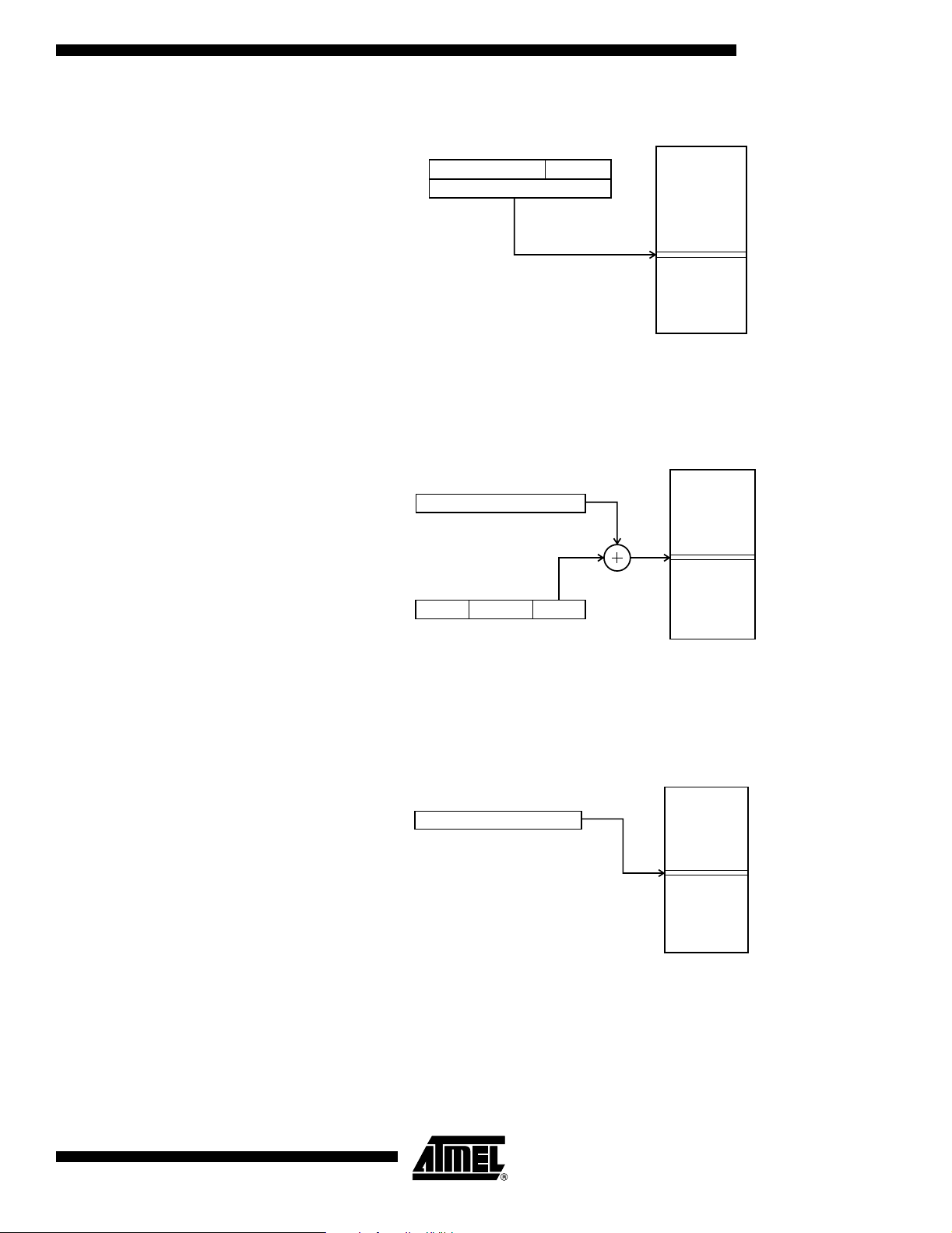
Data Direct Figure 14. Direct Data Addressing
31
OP Rr/Rd
16 LSBs
15 0
A 16-bit Data Address is contained in the 16 LSBs of a two-word instruction. Rd/Rr
specify the destination or source register.
20 19
AT86RF401
Data Space
16
$00
$DF
Data Indirect with
Figure 15. Data Indirect with Displacement
Displacement
15
Y OR Z - REGISTER
15
OP an
Operand address is the result of the Y or Z register contents added to the address contained in 6 bits of the instruction word.
Data Indirect Figure 16. Data Indirect Addressing
X, Y OR Z - REGISTER
Data Space
0
05610
Data Space
015
$00
$DF
$0000
1424D–RKE–09/02
$DF
Operand address is the contents of the X, Y or Z register.
23
Page 24

Data Indirect with Pre-decrement
Figure 17. Data Indirect Addressing with Pre-decrement
Data Space
015
X, Y OR Z - REGISTER
-1
$0000
$DF
The X, Y or Z register is decremented before the operation. Operand address is the
decremented contents of the X, Y or Z register.
Data Indirect with
Figure 18. Data Indirect Addressing with Post-increment
Post-increment
The X, Y or Z register is incremented after the operation. Operand address is the content of the X, Y or Z register prior to incrementing.
Constant Addressing Using the LPM Instruction
Figure 19. Code Memory Constant Addressing
X, Y OR Z - REGISTER
Data Space
015
1
$0000
$DF
24
$3FF
Constant byte address is specified by the Z register contents. The 10 MSBs select word
address (0–1K). For LPM, the LSB selects low byte if cleared (LSB = 0) or high byte if
set (LSB = 1).
AT86RF401
1424D–RKE–09/02
Page 25

AT86RF401
Indirect Program Addressing, IJMP and ICALL
Relative Program Addressing, RJMP and RCALL
Figure 20. Indirect Program Memory Addressing
$3FF
Program execution continues at address contained by the Z register (i.e., the PC is
loaded with the contents of the Z register).
Figure 21. Relative Program Memory Addressing
1
$3FF
Program execution continues at address PC + k + 1. The relative address k is from −
2048 to 2047.
1424D–RKE–09/02
25
Page 26

EEPROM Data Memory The AT86RF401 contains 128 bytes of data EEPROM memory. It is organized as a sep-
arate data space in which single bytes can be read and written. The access between the
EEPROM and the CPU is described in the Memory Programming section (page 13).
Memory Access Times and Instruction Execution Timing
This section describes the general access timing concepts for instruction execution and
internal memory access.
The AVR CPU is driven by the System Clock Ø generated from the main oscillator for
the chip. A programmable clock divider generates this clock from the crystal oscillator
input.
Figure 22 shows the parallel instruction fetches and instruction executions enabled by
the Harvard architecture and the fast-access register file concept. This is the basic pipelining concept to obtain up to 1 MIPS per MHz with the corresponding unique results for
functions per cost, functions per clocks and functions per power unit.
Figure 22. The Parallel Instruction Fetches and Instruction Executions
T1 T2 T3 T4
System Clock Ø
1st Instruction Fetch
1st Instruction Execute
2nd Instruction Fetch
2nd Instruction Execute
3rd Instruction Fetch
3rd Instruction Execute
4th Instruction Fetch
Figure 23 shows the internal timing concept for the register file. In a single clock cycle,
an ALU operation using two register operands is executed, and the result is stored back
to the destination register.
Figure 23. Single Cycle ALU Operation
T1 T2 T3 T4
System Clock Ø
Total Execution Time
Register Operands Fetch
ALU Operation Execute
Result Write Back
The internal data SRAM access is performed in two System Clock cycles as described
in Figure 24.
26
AT86RF401
1424D–RKE–09/02
Page 27
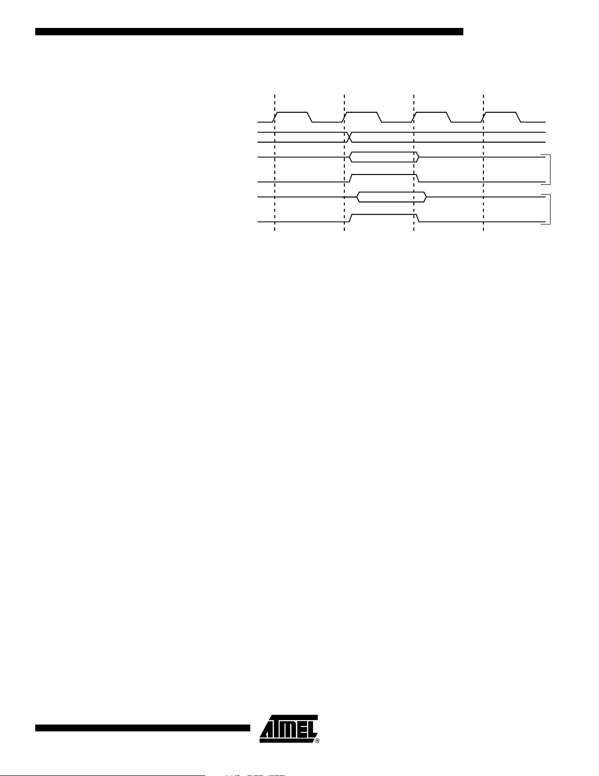
Figure 24. On-chip Data SRAM Access Cycles
T1 T2 T3 T4
System Clock Ø
AT86RF401
Address
Data
Write
Data
Read
Prev. Address
Address
All I/Os and peripherals are placed in the I/O space. The I/O locations are accessed by
the IN and OUT instructions, transferring data between the 32 general-purpose working
registers and the I/O space. I/O registers within the address range $00–$1F are directly
bit-accessible using the SBI and CBI instructions. In these registers, the value of single
bits can be checked by using the SBIS and SBIC instructions. Refer to Table 10,
“Instruction Set Manual,” on page 44 for more details. When using the I/O specific commands IN and OUT, the I/O addresses $00–$3F must be used. When addressing I/O
registers as SRAM, $20 must be added to these addresses.
For compatibility with future devices, reserved bits should be written to “0” if accessed.
Reserved I/O memory addresses should never be written.
Some of the status flags are cleared by writing a logical “1” to them. Note that the CBI
and SBI instructions will operate on all bits in the I/O register, writing a “1” back into any
flag read as set, thus clearing the flag. The CBI and SBI instructions work with registers
$00 to $1F only.
The I/O and peripherals control registers are explained in the following sections.
Write
Read
1424D–RKE–09/02
27
Page 28

I/O Memory
The I/O space definition of the AT86RF401 is shown in Table 7 below.
Table 7. AT86RF401 I/O Space Definitions
Address Hex Name Function
$3F SREG Status Register
$3E SPH Stack Pointer High Register (program to 0 x 00)
$3D SPL Stack Pointer Low Register
$35 BL_CONFIG Battery Low Configuration Register
$34 B_DET Button Detect Register
$33 AVR_CONFIG AVR Configuration Register
$32 IO_DATIN I/O DATA IN Register
$31 IO_DATOUT I/O DATA OUT Register
$30 IO_ENAB I/O Enable Register
$22 WDTCR Watchdog Timer Control Register
$21 BTCR Bit Timer Control Register
$20 BTCNT Bit Timer Count Register
$1E DEEAR Data EEPROM Address Register
$1D DEEDR Data EEPROM Data Register
$1C DEECR Data EEPROM Control Register
$17 LOCKDET2 Lock Detector Configuration Register 2
$16 VCOTUNE VCO Tuning Register
$14 PWR_ATTEN Power Attenuation Control Register
$12 TX_CNTL Transmitter Control Register
$10 LOCKDET1 Lock Detector Configuration Register 1
Note: Reserved and unused locations are not shown in the table.
28
AT86RF401
1424D–RKE–09/02
Page 29

AT86RF401
I/O and Control Registers
The AT86RF401 I/Os and peripherals are placed in the I/O space. The various I/O locations are accessed by the IN and OUT instructions transferring data between the 32
general-purpose working registers and the I/O space. I/O registers within the address
range $00–$1F are directly bit-accessible using the SBI and CBI instructions. In these
registers, the value of single bits can be checked by using the SBIS and SBIC instructions. Refer to Table 10 on page 44 for more details. The different I/O and peripherals
control registers are explained in the following sections.
Transmitter Control Register Descriptions
Lock Detector Configuration Register 1 – LOCKDET1
Bit 76543210
$10 –––UPOK ENKO BOD CS1 CS0
Read/Write R/W R/W R/W R/W R/W R/W R/W R/W
Initial Value 00000000
• Bits[7:5]
Reserved.
• Bit[4]: UPOK
If set high, this bit resets the unlock counter. The bit is level sensitive, and the unlock
counter will not count unless this bit is set to “0”. Leaving this bit high essentially disables the unlock detector.
• Bit[3]: ENKO (Enable Key on Bit)
If set to “1”, the rising edge of TXK starts the blackout period, during which any cycle
slips are ignored and do not affect the unlock circuit.
• Bit[2]: BOD (Black Out Disable)
When set high, cycle slips are counted immediately but only if LOCK is asserted high
(TX_CNTL b[2]).
• Bits[1:0] CS[1:0]: Cycle Slip Counter
These two bits determine how many cycle slips are allowed before the LOCKDETECT
signal is set low. The cycle slips are not counted unless the blackout logic is either disabled or the blackout window has passed.
CS[1:0] Functionality
00 1 cycle slip causes unlock condition
01 2 cycle slips cause unlock condition
10 3 cycle slips cause unlock condition
11 4 cycle slips cause unlock condition
1424D–RKE–09/02
29
Page 30

Transmit Control Register – TX_CNTL
Bit 76543210
$12 ––TXE TXK – LOC ––
Read/Write R/W R/W R/W R/W R/W R/W R/W R/W
Initial Value 00000000
• Bit[7:6]
Reserved.
• Bit[5]: TXE, Transmitter Enable
This bit turns on the transmitter.
• Bit[4]: TXK, Transmitter Key
ThisbitisORedwiththeoutputfromthebittimer.Ifthebittimerisusedtokeythetransmitter, the TXK bit should be programmed to “0”. If the bit timer is not used, this bit may
be used to manually key the transmitter.
Figure 25. Modulation Control Logic
Bit Timer
TXK
PLL
RF
IN
POWER
AMP
RF
OUT
ON/OFF
• Bit[3]
Reserved.
• Bit[2]: LOC, PLL Lock
This bit is set when the frequency synthesizer in the transmitter is locked. Usually this bit
should be set before transmitting.
Power Attenuation Control Register – PWR_ATTEN
Bit 76543210
$14 ––PCC2 PCC1 PCC0 PCF2 PCF1 PCF0
Read/Write R/W R/W R/W R/W R/W R/W R/W R/W
Initial Value 00000000
This register is used to select the power attenuation level. The total power attenuation is
the sum of the coarse attenuation and fine attenuation. As an example, to obtain 15 dB
of attenuation, the coarse setting of 12 dB and fine setting of 3 dB would be selected. To
obtain 12 dB coarse attenuation, Bits[5:3] would be set to [010]. To obtain 3 dB of fine
attentuation would require Bits[2:0] to be set to [011].
• Bits[7:6]
Reserved
30
AT86RF401
1424D–RKE–09/02
Page 31

• Bits[5:3]: PCC, Power Control (coarse)
Attenuates the output power in 6 dB steps.
PCC[5:3] Output Attenuation
000 0 dB
001 6 dB
010 12 dB
011 18 dB
100 24 dB
101 30 dB
110 Invalid
111 Invalid
• Bits[2:0]: PCF, Power Control (fine)
Attenuates the output power in 1 dB steps.
PCF[2:0] Output Attenuation
AT86RF401
000 0 dB
001 1 dB
010 2 dB
011 3 dB
100 4 dB
101 5 dB
110 Invalid
111 Invalid
VCO Tuning Register 6 – VCOTUNE
Bit 76543210
VCOVDET[1] VCOVDET[0] – VCOTUNE[4] VCOTUNE[3] VCOTUNE[2] VCOTUNE[1] VCOTUNE[0]
$16
Read/Write R R R/W R/W R/W R/W R/W R/W
Initial Value **000000
Note: * These values are unknown at initial startup.
• Bits[4:0]: VCO Tuning Capacitor Array
This device requires the use of an external inductor to tune the VCO. Tolerance of the
inductor, coupled with process variation of the device, can lead to variations in the tuning point of the VCO. A switched array of tuning capacitors has been added internally to
thedeviceinorderto“fine tune” the VCO. This capacitance is switched across pins 3
1424D–RKE–09/02
31
Page 32

and 4 (L1 and L2) of the device. The capacitor array is set by VCOTUNE[4:0] and is
comprised of the following switched capacitance levels:
VCOTUNE[4:0] Capacitance (pF)
00000 0
00001 0.03
00010 0.06
00011 0.09
00100 0.12
00101 0.15
00110 0.18
00111 0.21
01000 0.24
01001 0.27
01010 0.30
01011 0.33
01100 0.36
01101 0.39
01110 0.42
01111 0.45
10000 0.48
10001 0.51
10010 0.54
10011 0.57
10100 0.60
10101 0.63
10110 0.66
10111 0.69
11000 0.72
11001 0.75
11010 0.78
11011 0.81
11100 0.84
11101 0.87
11110 0.90
11111 0.93
32
AT86RF401
1424D–RKE–09/02
Page 33

AT86RF401
• Bits[7:6]: VCO Voltage Detector
The VCO Voltage Detector circuit monitors the level of the VCO control voltage. This circuit, along with the VCO Switch Caps and the Lock Detect circuit, is intended for use
with a software algorithm to tune the VCO such that the VCO control voltage is centered
approximately at 1.1V.
The Voltage Detector circuit consists of two comparators with fixed reference voltages
of V1 (lower reference voltage) and V2 (upper reference voltage). The VCO Control
Voltage is compared to these two reference voltages and generates the state table
listed in Table 8. The state of these comparators is output to Bits 7 and 6 (Vcodet[1:0])
of the VCOTUNE register.
Table 8. VCO Window Comparator States
VCOvdet[1:0] VCO Control Voltage
00
01
10
11 Not a valid state.
Above lower comparator threshold and below upper comparator
threshold. Control Voltage is within the valid window of operation.
Below both thresholds. Control Voltage is outside the recommended
window of operation.
Above both thresholds. Control Voltage is outside the recommended
window of operation.
Lock Detector Configuration Register 2 – LOCKDET2
Bit 76543210
$17 EUD LAT ULC[2] ULC[1] ULC[0] LC[2] LC[1] LC[0]
Read/Write R/W R/W R/W R/W R/W R/W R/W R/W
Initial Value 00000000
• Bit[7]: EUD
A “1” enables the unlock detect logic.
• Bit[6]: LAT (Lock Always True)
Forces the lockdetect signal to “1” at the output of the lock detect circuitry. This may be
useful if the lock detect signal is not going high for some reason, and a power amp interlock has been implemented, and the user wishes to enable the power amp output stage.
1424D–RKE–09/02
33
Page 34

• Bit[5:3]: ULC[2:0]
The unlock count (ULC) bits count a certain number of reference clocks, after which the
unlock detect circuit looks for a number of cycle slips determined by CS[1:0] before
making the loc detect signal go low. The ULC bits essentially control the blackout period
of the unlock detect circuit. The unlock counter is reset by the KEY signal rising (if
ENKO is asserted), or by the LOC rising edge, or by the UPOK signal being set high.
Number of REF
ULC[2:0]
000 8
001 16
010 32
011 64
100 128
101 256
110 512
111 1024
Clocks of Delay
• Bits[2:0]: LC[2:0]
The Lock Count (LC) bits control a counter that, after a number of reference clocks,
cause lock detect to go high. This counter will reset if a cycle slip or a reset signal occurs
(which happens if TXE goes low), if an out-of-lock condition occurs, if the crystal oscillator frequency is too low, or if the VCO feedback frequency is too low.
LC[2:0] Number of REF Clocks of Delay
000 8
001 16
010 32
011 64
100 128
101 256
110 512
111 1024
34
AT86RF401
1424D–RKE–09/02
Page 35

EEPROM Control Register Descriptions
Data EEPROM Control Register – DEECR
Bit 76543210
$1C ––––BSY EEU EEL EER
Read/Write R/W R/W R/W R/W R R/W R/W R/W
Initial Value 0 00000000
• Bits[7:4]
Reserved. These bits should be “ 0 ” when written; otherwise, results will be
unpredictable.
• Bit[3]: EEPROM Busy Bit
Initially set to “0”. This bit will be set high during writes to the EEPROM.
• Bit[2]: EEPROM Unlock Bit
Set this bit to “1” before writing the EEPROM. Reset this bit to “0” after the write is complete. This bit should be left in the zero state when the EEPROM is not being used,
which will protect the EEPROM data during power transients.
AT86RF401
• Bit[1]: EEPROM Load Bit
To write the EEPROM, use the following procedure:
Note: Because of noise and power considerations, the EEPROM should not be written while
the transmitter is enabled.
1. Set the unlock bit.
2. Write the address of the first byte to the DEEAR.
3. Set the load bit. This locks the page address in the DEEAR. Keep the unlock bit
set.
4. Write the desired data to the DEEDR register. This byte is loaded into the
EEPROM and will be written when the load bit is later deasserted.
5. If it is desired to write another byte in the same page, write the new address to
the DEEAR register, and a new byte to the DEEDR register. Continue until all
bytes that are to be written are loaded into the EEPROM. Bytes may only be
loaded to an address once. There are eight bytes per page.
6. Deassert the load bit. This starts the write operation. Some time after load is
deasserted, the busy bit will go high. Another read or write operation may not be
started until the busy bit has returned to “0”. Writes take approximately 4 ms to
complete. Again, the unlock bit must still be set when deasserting the load bit.
7. After all writes are complete, write “0” to the unlock bit.
• Bit[0]: EEPROM Read Bit
To read the EEPROM use the following procedure:
1. Write the address to the DEEAR.
2. Set the read bit.
3. Read the data register. The read bit will reset itself.
4. If another read needs to be done, repeat steps 1–3 again.
1424D–RKE–09/02
35
Page 36

Data EEPROM Data Register – DEEDR
Bit 76543210
$1D ED7 ED6 ED5 ED4 ED3 ED2 ED1 ED0
Read/Write R/W R/W R/W R/W R/W R/W R/W R/W
Initial Value 0 00000000
• Bits[7:0]
This register contains the byte to be written to EEPROM. If a read operation has been
done, this register contains that last byte read from the data EEPROM.
Data EEPROM Address Register – DEEAR
Bit 76543210
$1E – PA6 PA5 PA4 PA3 BA2 BA1 BA0
Read/Write R/W R/W R/W R/W R/W R/W R/W R/W
Initial Value 0 00000000
• Bit[7]
Reserved.
• Bits[6:3]: Data EEPROM Page Address
These bits select the page in the EEPROM that is to be accessed. These bits are write
locked and cannot be altered when the load bit is set.
• Bits[2:0]: Data EEPROM Byte Address
These bits select the byte in the page that is to be accessed. During a page write operation, these bits are used in combination with the DEEDR register to write bytes into a
page.
36
AT86RF401
1424D–RKE–09/02
Page 37

Bit Timer Register Descriptions
Bit Timer Count Register – BTCNT
Bit 76543210
$20 C7 C6 C5 C4 C3 C2 C1 C0
Read/Write R/W R/W R/W R/W R/W R/W R/W R/W
Initial Value 00000000
• Bit [7:0]
Lowest 8 bits of
determines a counter value that sets the width of a mark or a space that is sent to the
transmitter. The width of the mark or space is:
P
XX=PAVR
P
where
that is determined by the ACS bits of the AVR configuration register, AVR_CONFIG.
Bit Timer Control Register – BTCR
XX
countval
*
(countval
. When combined with bits [7:6] of the BTCR register,
+1)
is the period of the mark or space, and
AT86RF401
P
is the period of the AVR clock
AVR
countval
Bit 76543210
$21 C9 C8 M1 M0 IE F2 DATA F0
Read/Write R/W R/W R/W R/W R/W R R/W R
Initial Value 00000000
• Bit[7:6]
Count_val[9:8]. MSB of BTCNT counter value bits.
• Bits[5:4]
Bit Timer Mode.
Mode[1:0] Bit Timer Function
00 Bit Timer Disabled
01 Transmit Mode, Transmitter Not Keyed
10 Receive Mode
11 Transmit Mode, Transmitter Keyed
• Bit[3]: Interrupts Enabled
If this bit is set, the Flag2 and Flag0 will generate their respective interrupts when they
are set. Flag0 interrupt vector is located at 0 x 04. Flag2 interrupt vector is located at
0 x 02. Typically, a JMP instruction resides at these vector locations to pass control to
an interrupt handler. For Flag0 only, slightly faster execution can be achieved if the JMP
instruction is eliminated, and the interrupt service routine is located beginning at 0 x 04.
1424D–RKE–09/02
37
Page 38

• Bit[2]: Flag2
In transmit mode, this flag indicates the Transmit Done condition that occurs when the
buffer is empty and the counter has counted down to “0”. In receive mode, this flag indicates that an edge has occurred, and the AVR should process the count value in the
BTCR and BTCNT registers. This bit is cleared upon read, e.g., IN R16, BTCR.
Mode[1:0] Flag2 Function
00 Disabled
01
10 An edge has been detected at the IO3 pin.
11
Indicates Transmit Done condition; buffer is empty and the
counter has expired.
Indicates Transmit Done condition; buffer is empty and the
counter has expired.
• Bit[1]: Data Bit
In transmit mode, this is a one-bit buffer that the AVR writes data to and the bit timer
extracts data from. When the bit timer removes the value from this register, the Flag0 bit
is set, and if enabled, an interrupt (INT2) is generated. If the interrupt is used, the ISR
should load a new bit into the buffer. If the interrupt is not enabled, then a polling method
should be used to detect Flag0 being set. Because of overhead associated with interrupt
handling, it may be slightly faster to use polling.
In receive mode, the value in this register indicates whether the edge at the IO3 pin was
rising or falling. A “1” indicates a rising edge occurred, and a “0” indicates that a falling
edge was detected. The number of AVR clock cycles since the last edge is held in the
C[9:0] (
countval
) bits (that is, unless an overflow condition has occurred).
• Bit[0]: Flag0
In transmit mode, this flag indicates the buffer is empty and the AVR should load new
data into it. In receive mode, this indicates a counter overflow condition has occurred.
The AVR should increment its software counter if this condition has occurred. This bit is
cleared upon read, e.g., IN R16, BTCR.
Watchdog Timer Control Register – WDTCR
Bit 76543210
$22 –––WDTOE WDE WDP2 WDP1 WDP0 WDTCR
Read/Write R R R R/W R/W R/W R/W R/W
Initial Value 00000000
• Bits[7:5]
Reserved. These bits will always read as “0”.
• Bit[4]: WDTOE, Watchdog Turn-off Enable
This bit must be set (“1”) when the WDE bit is cleared. Otherwise, the watchdog will not
be disabled. Once set, hardware will clear this bit to “0” after four clock cycles. Refer to
the description of the WDE bit for a watchdog disable procedure.
• Bit[3]: WDE, Watchdog Enable
When the WDE is set (“1”), the Watchdog Timer is enabled, and if the WDE is cleared
(“0”), the Watchdog Timer function is disabled. WDE can only be cleared if the WDTOE
38
AT86RF401
1424D–RKE–09/02
Page 39

AT86RF401
bit is set (“1”). To disable an enabled Watchdog Timer, the following procedure must be
followed: In the same operation, write a logical “1” to WDTOE and WDE. A logical “1”
must be written to WDE even though it is set to “1” before the disable operation starts.
Within the next four clock cycles, write a logical “0” to WDE. This disables the watchdog.
• Bits[2:0]: WDP2, WDP1, WDP0, Watchdog Timer Prescaler 2, 1 and 0
The WDP2, WDP1 and WDP0 bits determine the Watchdog Timer prescaling when the
Watchdog Timer is enabled. The different prescaling values and their corresponding
time-out periods are shown in Table 9.
Table 9. Watchdog Timer Prescale Select
WDP2 WDP1 WDP0 Number of System Clock Cycles
0 0 0 2,048 cycles
0 0 1 4,096 cycles
0 1 0 8,192 cycles
0 1 1 16,384 cycles
1 0 0 32,768 cycles
1 0 1 65,536 cycles
I/O Enable Register – IO_ENAB
Bit 76543210
$30 – BOHYST IOE5 IOE4 IOE3 IOE2 IOE1 IOE0
Read/Write R/W R/W R/W R/W R/W R/W R/W R/W
Initial Value 00000000
1 1 0 131,072 cycles
1 1 1 262,144 cycles
Note:
T
wdt
XTALB
period
ACS
div
WDT
××=
div
Example:
If the crystal period is 50 ns and the system clock divider is set to 32 (Bits[7:5] in the
PWR_CTL register are set to 010) and the WDT prescaler is set to 32K, then:
Watchdog Timeout = 50 ns × 32 × 32768 = 52 ms
• Bit[7]
Reserved.
• Bit[6]
If set to “1”, additional hysteresis is added to the battery low and brown-out logic. See
BL_CONFIG register description and Table 3 (page 10) for more details.
1424D–RKE–09/02
39
Page 40

• Bits[5:0]
If set to “1”, the corresponding bit (pin) IO[5:0] is configured as an output. Data may then
be written to that output by writing to the IO_DATA register. If set to “0”, the corresponding bit (pin) may be either a button input (refer to the Button Detect Register, $34) used
to wake the part up or a normal digital input.
I/O Data Out Register – IO_DATOUT
Bit 76543210
$31 ––IOO5 IOO4 IOO3 IOO2 IOO1 IOO0
Read/Write R R R/W R/W R/W R/W R/W R/W
Initial Value 00000000
• Bits[7:6]: Reserved
These bits read “0”.
IO_ENAB[n] IO_DATOUT[n] IO[n]
0 0 Normal Input
0 1 Button Input
1 0 Output Driven Low
1 1 Output Driven High
• Bits[5.0]
If enabled in the IO_ENAB register and not in test mode, the data in Bits[5:0] goes to the
corresponding general-purpose output IO [5:0].
I/O Data In Register – IO_DATIN
Bit 76543210
$32 ––IOI5 IOI4 IOI3 IOI2 IOI1 IOI0
Read/Write R/WR/WRRRRRR
Initial Value 00
• Bits[7:6]: Reserved
This bit reads “0”.
• Bits[5:0]
These bits directly read the data from the I/O pins IO[5:0]. Writes to these bits have no
effect.
AVR Configuration Register – AVR_CONFIG
Bit 76543210
$33 – ACS1 ACS0 TM BD BLI SLEEP BBM
Read/Write R/W R/W R/W R/W R R W R/W
Initial Value 00000000
40
AT86RF401
1424D–RKE–09/02
Page 41

AT86RF401
• Bits[6:5]: AVR System Clock Select
These bits select the divide value of the XTALB input that is used to produce the AVR
System Clock.
ACS[1:0] AVR System Clock
11 XTALB/16
10 XTALB/32
01 XTALB/64
00 XTALB/128
This clock select value may be programmed on the fly by either the AVR processor in
normal operation or by an I/O write SPI command during SPI mode. Note that during
SPI mode, the I/O and serial programming logic runs at XTALB/16 frequency.
• Bit[4]: Test Mode
When this bit is set to “1”, the part enters test mode. The I/O pins, if enabled, assume
the following functionality:
I/O5 I/O4 I/O3 I/O2 I/O1 I/O0
Normal Mode
(RESETB = 1)
SPI Mode
(RESETB = 0)
Notes: 1. IO_ENAB register is NOT used for SPI pins.
2. In SPI mode, the I/O registers may be directly accessed via the SPI interface. Txkey, lockdetect may be output using this
mode.
txkey
(Output)
txkey
(Output)
lockdetect
(Output)
lockdetect
(Output)
• Bit[3]: Battery Dead
Indicates battery is dead. Only readable by SPI interface.
• Bit[2]: Battery Low Indicator
This bit is identical to Bit[7] of Battery Low Configuration Register ($35). When Bit[6] of
Battery Low Configuration Register ($35) is set (Battery Low Valid), a set bit in this location indicates that the battery voltage is lower than the voltage level that is determined
by Bits[5:0] of Battery Low Configuration Register ($35).
• Bit [1]: Sleep Bit
When set, this bit stops the crystal oscillator. This stops the AVR processor with the program counter frozen at the current instruction. Sleep will also stop the Watchdog Timer.
The Watchdog Timer is only restarted if the part wakes up. If an I/O pin is configured as
a button, a button press will start the oscillator and check the battery level. If the battery
level is greater than the Battery Dead level, the AVR system clock is started and normal
program execution continues. If the battery level is below the Battery Dead level, the
crystal oscillator is turned off, putting the part back to sleep until a button is pressed
again (care should be taken not to put the part to sleep unless a button is configured and
enabled).
txenable
(Output)
txenable
(Output)
RFU RFU RFU
SPI_CLK SDO SDI
1424D–RKE–09/02
• Bit[0]: Button Boot Mode (BBM)
If the BBM bit is set and the part is brought out of sleep mode by a button input activation, the part will enter the button reset state. In this state, the part will reboot and begin
code execution at the reset location. This bit is reset at POR and when exiting the button
reset state. All other registers remain unchanged.
41
Page 42

Button Detect Register – B_DET
Bit 76543210
$34 ––BD5 BD4 BD3 BD2 BD1 BD0
Read/Write R R R/W R/W R/W R/W R/W R/W
Initial Value 00000000
• Bits[7:6]
Reserved. These bits read “0”.
• Bits[5:0]
When an I/O pin is configured as a button using the IO_ENAB and IO_DATOUT registers and a logic low is detected on that pin, the button detect logic is activated. If the part
is in sleep mode, the part responds as described in the Power Control Register description. If a good battery is present, the appropriate bit is set in this register. A bit in this
register is cleared by writing a “0” to it.
Battery Low Configuration Register – BL_CONFIG
Bit 76543210
$35 BL BLV BL5 BL4 BL3 BL2 BL1 BL0
Read/Write R R R/W R/W R/W R/W R/W R/W
Initial Value 00000000
• Bit[7]: Battery Low
When Bit 6 in this register is set (Battery Low Valid), the BL (Battery Low) bit indicates
that the battery voltage is lower than the voltage level that is determined by Bits [5:0] of
this register.
• Bit[6]: Battery Low Valid
When the Battery Low Configuration Register is written, this bit is set to “0”. When the
battery voltage has been sampled and compared to the voltage determined by the BLx
bits, this bit is set to “1” indicating that the data in Bit 7 (Battery Low) is valid. This can
take up to 3100 XTAL cycles to complete.
• Bit[5:0]: Battery Low Detection Level
This value is sent to the battery monitor. The threshold is calculated using the formulas
shown in Table 3 (page 10).
42
AT86RF401
1424D–RKE–09/02
Page 43

AT86RF401
The Stack Pointer – SP The Stack Pointer is implemented as two 8-bit registers in the I/O space locations $3E
($5E) and $3D ($5D). Caution: As the data memory has 224 locations, only 8 bits are
used and the SPH register must be programmed to 0 x 00.
Bit 15 14 13 12 11 10 9 8
$3E –––––SP10 SP9 SP8 SPH
$3D SP7 SP6 SP5 SP4 SP3 SP2 SP1 SP0 SPL
76543210
Read/Write RRRRRR/WR/WR/W
R/W R/W R/W R/W R/W R/W R/W R/W
Initial Value 00000000
00000000
The Stack Pointer points to the data SRAM stack area where the Subroutine and Interrupt Stacks are located. This stack space in the data SRAM must be defined by the
program before any subroutine calls are executed or interrupts are enabled. The Stack
Pointer must be set to point above $60. The Stack Pointer is decremented by one when
data is pushed onto the stack with the PUSH instruction, and it is decremented by two
when the return address is pushed onto the stack with subroutine call and interrupt. The
Stack Pointer is incremented by one when data is popped from the stack with the POP
instruction, and it is incremented by two when data is popped from the stack with Return
from Subroutine (RET) or Return from Interrupt (RETI).
The Status Register – SREG The AVR status register – SREG – at I/O space location $3F is defined as:
Bit 76543210
$3F ITHSVNZC
Read/Write R/W R/W R/W R/W R/W R/W R/W R/W
Initial Value 00000000
• Bit[7] – I: Global Interrupt Enable
The global interrupt enable bit must be set (“1”) for the interrupts to be enabled. The
individual interrupt enable control is then performed in the interrupt mask registers
(GIMSK/TIMSK). If the global interrupt enable register is cleared (“0”), none of the interrupts are enabled, independent of the GIMSK/TIMSK values. The I-bit is cleared by
hardware after an interrupt has occurred and is set by the RETI instruction to enable
subsequent interrupts.
• Bit[6] – T: Bit Copy Storage
The bit copy instructions BLD (Bit LoaD) and BST (Bit STore) use the T-bit as source
and destination for the operated bit. A bit from a register in the register file can be copied
into T by the BST instruction, and a bit in T can be copied into a bit in a register in the
register file by the BLD instruction.
• Bit[5] – H: Half Carry Flag
The half carry flag H indicates a half carry in some arithmetic operations. See Table 10,
“SRAM Organization,” on page 21 for detailed information.
1424D–RKE–09/02
43
Page 44

Table 10. Instruction Set
• Bit[4] – S: Sign Bit, S = N⊕V
The S-bit is always an exclusive or between the negative flag N and the two’s complement overflow flag V. See Table 10 for detailed information.
• Bit[3] – V: Two’s Complement Overflow Flag
The two’s complement overflow flag V supports two’s complement arithmetics. See
Table 10 below for detailed information.
• Bit[2] – N: Negative Flag
The negative flag N indicates a negative result after the different arithmetic and logic
operations. See Table 10 below for detailed information.
• Bit[1] – Z: Zero Flag
The zero flag Z indicates a zero result after the different arithmetic and logic operations.
See Table 10 below for detailed information.
• Bit[0] – C: Carry Flag
The carry flag C indicates a carry in an arithmetic or logic operation. See Table 10 for
detailed information.
Mnemonics
Arithmetic and Logic Instructions
ADD Rd, Rr Add Two Registers Rd ← Rd + Rr Z,C,N,V,H
ADC Rd, Rr Add with Carry Two Registers Rd ← Rd + Rr + C Z,C,N,V,H 1
ADIW Rdl,K Add Immediate to Word Rdh:Rdl ← Rdh:Rdl + K Z,C,N,V,S 1
SUB Rd, Rr Subtract Two Registers Rd ← Rd - Rr Z,C,N,V,H 2
SUBI Rd, K Subtract Constant from Register Rd ← Rd - K Z,C,N,V,H 1
SBC Rd, Rr Subtract with Carry Two Registers Rd ← Rd-Rr-C Z,C,N,V,H 1
SBCI Rd, K Subtract with Carry Constant from
SBIW Rdl,K Subtract Immediate from Word Rdh:Rdl ← Rdh:Rdl - K Z,C,N,V,S 1
AND Rd, Rr Logical AND Registers Rd ← Rd • Rr Z,N,V 2
ANDI Rd, K Logical AND Register and
OR Rd, Rr Logical OR Registers Rd ← Rd v Rr Z,N,V 1
ORI Rd, K Logical OR Register and Constant Rd ← Rd v K Z,N,V 1
EOR Rd, Rr Exclusive OR Registers Rd ← Rd ⊕ Rr Z,N,V 1
COM Rd One’s Complement Rd ← $FF − Rd Z,C,N,V 1
Operands Description Operation Flags #Clocks
Rd ← Rd-K-C Z,C,N,V,H 1
Register
Rd ← Rd • KZ,N,V1
Constant
NEG Rd Two’s Complement Rd ← $00 − Rd Z,C,N,V,H 1
SBR Rd,K Set Bit(s) in Register Rd ← Rd v K Z,N,V 1
CBR Rd,K Clear Bit(s) in Register Rd ← Rd • ($FF - K) Z,N,V 1
INC Rd Increment Rd ← Rd + 1 Z,N,V 1
DEC Rd Decrement Rd ← Rd − 1Z,N,V1
TST Rd Test for Zero or Minus Rd ← Rd • Rd Z,N,V 1
44
AT86RF401
1424D–RKE–09/02
Page 45

Table 10. Instruction Set (Continued)
AT86RF401
Mnemonics
CLR Rd Clear Register Rd ← Rd ⊕ Rd Z,N,V 1
SER Rd Set Register Rd ← $FF None 1
Branch Instructions
RJMP k Relative Jump PC ← PC+k+1 None 1
IJMP Indirect Jump to (Z) PC ← Z None 2
JMP k Direct Jump PC ← k None 2
RCALL k Relative Subroutine Call PC ← PC+k+1 None 3
ICALL Indirect Call to (Z) PC ← Z None 3
CALL k Direct Subroutine Call PC ← k None 3
RET Subroutine Return PC ← STACK None 4
RETI Interrupt Return PC ← STACK I 4
CPSE Rd,Rr Compare, Skip if Equal if (Rd = Rr) PC ← PC + 2 or 3 None 1/2/3
CP Rd,Rr Compare Rd − Rr Z, N,V,C,H 1
CPC Rd,Rr Compare with Carry Rd − Rr − C Z, N,V,C,H 1
CPI Rd,K Compare Register with Immediate Rd − K Z, N,V,C,H 1
SBRC Rr, b Skip if Bit in Register Cleared If (Rr(b)=0) PC ← PC + 2 or 3 None 1/2/3
SBRS Rr, b Skip if Bit in Register Set If (Rr(b)=1) PC ← PC + 2 or 3 None 1/2/3
Operands Description Operation Flags #Clocks
SBIC P, b Skip if Bit in I/O Register Cleared If (P(b)=0) PC ← PC + 2 or 3 None 1/2/3
SBIS P, b Skip if Bit in I/O Register Set If (P(b)=1) PC ← PC + 2 or 3 None 1/2/3
BRBS s, k Branch if Status Flag Set If (SREG(s) = 1) then PC ← PC + k + 1 None 1/2
BRBC s, k Branch if Status Flag Cleared If (SREG(s) = 0) then PC ← PC + k + 1 None 1/2
BREQ k Branch if Equal If (Z = 1) then PC ← PC + k + 1 None 1/2
BRNE k Branch if Not Equal If (Z = 0) then PC ← PC + k + 1 None 1/2
BRCS k Branch if Carry Set If (C = 1) then PC ← PC + k + 1 None 1/2
BRCC k Branch if Carry Cleared If (C = 0) then PC ← PC + k + 1 None 1/2
BRSH k Branch if Same or Higher If (C = 0) then PC ← PC + k + 1 None 1/2
BRLO k Branch if Lower If (C = 1) then PC ← PC + k + 1 None 1/2
BRMI k Branch if Minus If (N = 1) then PC ← PC + k + 1 None 1/2
BRPL k Branch if Plus If (N = 0) then PC ← PC + k + 1 None 1/2
BRGE k Branch if Greater or Equal, Signed If (N ⊕ V= 0) then PC ← PC + k + 1 None 1/2
BRLT k Branch if Less Than Zero, Signed If (N ⊕ V= 1) then PC ← PC + k + 1 None 1/2
BRHS k Branch if Half Carry Flag Set If (H = 1) then PC ← PC + k + 1 None 1/2
BRHC k Branch if Half Carry Flag Cleared If (H = 0) then PC ← PC + k + 1 None 1/2
BRTS k Branch if T Flag Set If (T = 1) then PC ← PC + k + 1 None 1/2
BRTC k Branch if T Flag Cleared If (T = 0) then PC ← PC + k + 1 None 1/2
BRVS k Branch if Overflow Flag Set If (V = 1) then PC ← PC + k + 1 None 1/2
1424D–RKE–09/02
45
Page 46

Table 10. Instruction Set (Continued)
Mnemonics
BRVC k Branch if Overflow Flag Cleared If (V = 0) then PC ← PC + k + 1 None 1/2
BRIE k Branch if Interrupt Enabled If (I = 1) then PC ← PC + k + 1 None 1/2
BRID k Branch if Interrupt Disabled If (I = 0) then PC ← PC + k + 1 None 1/2
Data Transfer Instructions
MOV Rd, Rr Move Between Registers Rd ← Rr None 1
MOVW Rd, Rr Copy Register Word Rd+1:Rd ← Rr + 1:Rr None
LDI Rd, K Load Immediate Rd ← K None 1
LD Rd, X Load Indirect Rd ← (X) None 2
LD Rd, X+ Load Indirect and Post-Inc. Rd ← (X), X ← X + 1 None 2
LD Rd, −X Load Indirect and Pre-Dec. X ← X − 1, Rd ← (X) None 2
LD Rd, Y Load Indirect Rd ← (Y) None 2
LD Rd, Y+ Load Indirect and Post-Inc. Rd ← (Y), Y ← Y + 1 None 2
LD Rd, −Y Load Indirect and Pre-Dec. Y ← Y − 1, Rd ← (Y) None 2
LDD Rd,Y+q Load Indirect with Displacement Rd ← (Y + q) None 2
LD Rd, Z Load Indirect Rd ← (Z) None 2
LD Rd, Z+ Load Indirect and Post-Inc. Rd ← (Z), Z ← Z + 1 None 2
LD Rd, −Z Load Indirect and Pre-Dec. Z ← Z − 1, Rd ← (Z) None 2
Operands Description Operation Flags #Clocks
LDD Rd, Z+q Load Indirect with Displacement Rd ← (Z+q) None 2
LDS Rd, k Load Direct from SRAM Rd ← (k) None 2
ST X, Rr Store Indirect (X) ← Rr None 2
ST X+, Rr Store Indirect and Post-Inc. (X) ← Rr, X ← X + 1 None 2
ST − X, Rr Store Indirect and Pre-Dec. X ← X − 1, (X) ← Rr None 2
ST Y, Rr Store Indirect (Y) ← Rr None 2
ST Y+, Rr Store Indirect and Post-Inc. (Y) ← Rr, Y ← Y + 1 None 2
ST −Y, Rr Store Indirect and Pre-Dec. Y ← Y − 1, (Y) ← Rr None 2
STD Y+q,Rr Store Indirect with Displacement (Y + q) ← Rr None 2
ST Z, Rr Store Indirect (Z) ← Rr None 2
ST Z+, Rr Store Indirect and Post-Inc. (Z) ← Rr, Z ← Z + 1 None 2
ST −Z, Rr Store Indirect and Pre-Dec. Z ← Z − 1, (Z) ← Rr None 2
STD Z+q,Rr Store Indirect with Displacement (Z + q) ← Rr None 2
STS k, Rr Store Direct to SRAM (k) ← Rr None 2
LPM Load Program Memory R0 ← (Z) None 3
LPM Rd, Z Load Program Memory Rd ← (Z) None 3
LPM Rd, Z+ Load Program Memory and Post-
Inc.
Rd ← (Z), Z ← Z+1 None 3
IN Rd, P In Port Rd ← P None 1
46
AT86RF401
1424D–RKE–09/02
Page 47

Table 10. Instruction Set (Continued)
AT86RF401
Mnemonics
OUT P, Rr Out Port P ← Rr None 1
PUSH Rr Push Register on Stack STACK ← Rr None 2
POP Rd Pop Register from Stack Rd ← STACK None 2
Bit and Bit-test Instructions
SBI P, b Set Bit in I/O Register I/O(P,b) ← 1 None 2
CBI P, b Clear Bit in I/O Register I/O(P,b) ← 0 None 2
LSL Rd Logical Shift Left Rd(n+1) ← Rd(n), Rd(0) ← 0 Z,C,N,V 1
LSR Rd Logical Shift Right Rd(n) ← Rd(n+1), Rd(7) ← 0 Z,C,N,V 1
ROL Rd Rotate Left Through Carry
ROR Rd Rotate Right Through Carry
ASR Rd Arithmetic Shift Right Rd(n) ← Rd(n+1), n = 0...6 Z,C,N,V 1
SWAP Rd Swap Nibbles
BSET s Flag Set SREG(s) ← 1SREG(s)1
BCLR s Flag Clear SREG(s) ← 0SREG(s)1
BST Rr, b Bit Store from Register to T T ← Rr(b) T 1
BLD Rd, b Bit Load from T to Register Rd(b) ← T None 1
SEC Set Carry C ← 1C1
Operands Description Operation Flags #Clocks
Rd(0)← C, Rd(n+1)←Rd(n), C← Rd(7)
Rd(7)← C, Rd(n)←Rd(n+1), C← Rd(0)
Rd(3...0)← Rd(7...4), Rd(7...4)← Rd(3...0)
Z,C,N,V 1
Z,C,N,V 1
None 1
CLC Clear Carry C ← 0C1
SEN Set Negative Flag N ← 1N1
CLN Clear Negative Flag N ← 0N1
SEZ Set Zero Flag Z ← 1Z1
CLZ Clear Zero Flag Z ← 0Z1
SEI Global Interrupt Enable I ← 1I1
CLI Global Interrupt Disable I ← 0I1
SES Set Signed Test Flag S ← 1S1
CLS Clear Signed Test Flag S ← 0S1
SEV Set Two’s Complement Overflow V ← 1V1
CLV Clear Two’s Complement Overflow V ← 0V1
SET Set T in SREG T ← 1T1
CLT Clear T in SREG T ← 0T1
SEH Set Half Carry Flag in SREG H ← 1H1
CLH Clear Half Carry Flag in SREG H ← 0H1
NOP No Operation None 1
SLEEP Sleep Not Implemented None 3
WDR Watchdog Reset (See specific description for WDR/timer) None 1
1424D–RKE–09/02
47
Page 48

Ordering Information
Temperature
RF Output Ordering Code Package Application
315 MHz AT86RF401U 20T North American −40°Cto85°C
434 MHz AT86RF401E 20T European −40°Cto85°C
264 to 456 MHz AT86RF401X 20T All Applications −40°Cto85°C
Operating Range
48
AT86RF401
1424D–RKE–09/02
Page 49

AT86RF401
Package Drawing All devices are packaged on tape in reel; standard reel quantity is 2,500 pieces.
20A2–TSSO
b
L
L1
E1
E
End View
e
COMMON DIMENSIONS
Top View
SYMBOL
D 6.40 6.50 6.60 2, 5
A
A2
Side View
D
Notes: 1. This drawing is for general information only. Please refer to JEDEC Drawing MO-153, Variation AC, for additional
information.
2. Dimension D does not include mold Flash, protrusions or gate burrs. Mold Flash, protrusions and gate burrs shall
not exceed 0.15 mm (0.006 in) per side.
3. Dimension E1 does not include inter-lead Flash or protrusions. Inter-lead Flash and protrusions shall not exceed
0.25 mm (0.010 in) per side.
4. Dimension b does not include Dambar protrusion. Allowable Dambar protrusion shall be 0.08 mm total in excess
of the b dimension at maximum material condition. Dambar cannot be located on the lower radius of the foot.
Minimum space between protrusion and adjacent lead is 0.07 mm.
5. Dimension D and E1 to be determined at Datum Plane H.
2325 Orchard Parkway
R
San Jose, CA 95131
TITLE
20A2, 20-lead (4.4 x 6.5 mm Body), 0.65 pitch,
Thin Shrink Small Outline Package (TSSOP)
E 6.40 BSC
E1 4.30 4.40 4.50 3, 5
A ––1.20
A2 0.80 1.00 1.05
b 0.19 – 0.30 4
e 0.65 BSC
L 0.45 0.60 0.75
L1 1.00 REF
(Unit of Measure = mm)
MIN
NOM
DRAWING NO.
MAX
20A2 C
NOTE
6/3/02
REV.
1424D–RKE–09/02
49
Page 50

Atmel Headquarters Atmel Operations
Corporate Headquarters
2325 Orchard Parkway
San Jose, CA 95131
TEL 1(408) 441-0311
FAX 1(408) 487-2600
Europe
Atmel Sarl
Route des Arsenaux 41
Case Postale 80
CH-1705 Fribourg
Switzerland
TEL (41) 26-426-5555
FAX (41) 26-426-5500
Asia
Room 1219
Chinachem Golden Plaza
77 Mody Road Tsimhatsui
East Kowloon
Hong Kong
TEL (852) 2721-9778
FAX (852) 2722-1369
Japan
9F, Tonetsu Shinkawa Bldg.
1-24-8 Shinkawa
Chuo-ku, Tokyo 104-0033
Japan
TEL (81) 3-3523-3551
FAX (81) 3-3523-7581
Memory
2325 Orchard Parkway
San Jose, CA 95131
TEL 1(408) 441-0311
FAX 1(408) 436-4314
Microcontrollers
2325 Orchard Parkway
San Jose, CA 95131
TEL 1(408) 441-0311
FAX 1(408) 436-4314
La Chantrerie
BP 70602
44306 Nantes Cedex 3, France
TEL (33) 2-40-18-18-18
FAX (33) 2-40-18-19-60
ASIC/ASSP/Smart Cards
Zone Industrielle
13106 Rousset Cedex, France
TEL (33) 4-42-53-60-00
FAX (33) 4-42-53-60-01
1150 East Cheyenne Mtn. Blvd.
Colorado Springs, CO 80906
TEL 1(719) 576-3300
FAX 1(719) 540-1759
Scottish Enterprise Technology Park
Maxwell Building
East Kilbride G75 0QR, Scotland
TEL (44) 1355-803-000
FAX (44) 1355-242-743
RF/Automotive
Theresienstrasse 2
Postfach 3535
74025 Heilbronn, Germany
TEL (49) 71-31-67-0
FAX (49) 71-31-67-2340
1150 East Cheyenne Mtn. Blvd.
Colorado Springs, CO 80906
TEL 1(719) 576-3300
FAX 1(719) 540-1759
Biometrics/Imaging/Hi-Rel MPU/
High Speed Converters/RF Datacom
Avenue de Rochepleine
BP 123
38521 Saint-Egreve Cedex, France
TEL (33) 4-76-58-30-00
FAX (33) 4-76-58-34-80
e-mail
literature@atmel.com
Web Site
http://www.atmel.com
© Atmel Corporation 2002.
Atmel Corporation makes no warranty for the use of its products, other than those expressly contained in the Company’s standard warranty
whichisdetailedinAtmel’s Terms and Conditions located on the Company’s web site. The Company assumes no responsibility for any errors
which may appear in this document, reserves the right to change devices or specifications detailed herein at any time without notice, and does
not make any commitment to update the information contained herein. No licenses to patents or other intellectual property of Atmel are granted
by the Company in connection with the sale of Atmel products, expressly or by implication. Atmel’s products are not authorized for use as critical
components in life support devices or systems.
AT ME L®and AVR®are registered trademarks and SmartRF™is a trademark of Atmel.
™
Crystek
the trademarks of others.
is a registered trademark of Crystek Crystals Corporation. Other terms and product names may be
Printed on recycled paper.
1424D–RKE–09/02
 Loading...