

Page 1

Features
• High Performance RF-CMOS 2.4 GHz Radio Transceiver Targeted for IEEE 802.15.4
• Industry Leading Link Budget (104 dB)
• Ultra-Low Current Consumption:
• Ultra-Low Supply Voltage (1.8V to 3.6V) with Internal Regulator
• Optimized for Low BoM Cost and Ease of Production:
• Easy to Use Interface:
• Radio Transceiver Features:
• Special IEEE 802.15.4-2006 Hardware Support:
• MAC Hardware Accelerator:
• Extended Feature Set Hardware Support:
• Industrial Temperature Range:
• I/O and Packages:
• Compliant to IEEE 802.15.4-2006 and IEEE 802.15.4-2003
• Compliant to EN 300 328/440, FCC-CFR-47 Part 15, ARIB STD-66, RSS-210
™
ZigBee
and ISM Applications
– Receiver Sensitivity -101 dBm
– Programmable Output Power from -17 dBm up to +3 dBm
–
SLEEP
–
TRX_OFF
–
RX_ON
–
BUSY_TX
– Few External Components Necessary (Crystal, Capacitors and Antenna)
– Excellent ESD Robustness
– Registers, Frame Buffer and AES Accessible through Fast SPI
– Only Two Microcontroller GPIO Lines Necessary
– One Interrupt Pin from Radio Transceiver
– Clock Output with Prescaler from Radio Transceiver
– 128-byte FIFO (SRAM) for Data Buffering
– Programmable Clock Output, to Clock the Host Microcontroller or as Timer
Reference
– Integrated RX/TX Switch
– Fully Integrated, Fast Settling PLL to support Frequency Hopping
– Battery Monitor
– Fast Wake-Up Time < 0.25 msec
– FCS Computation and Clear Channel Assessment
– RSSI Measurement, Energy Detection and Link Quality Indication
– Automated Acknowledgement, CSMA-CA and Retransmission
– Automatic Address Filtering
– Automated FCS Check
– AES 128bit Hardware Accelerator
– RX/TX Indication (external RF Front-End Control)
– RX Antenna Diversity
– Supported PSDU data rates: 250 kb/s, 500 kb/s, 1 Mb/s and 2 Mb/s
– True Random Number Generation for Security Application
– -40° C to +85° C
– 32-pin Low-Profile QFN Package 5 x 5 x 0.9 mm³
– RoHS/Fully Green
=
0.02 µA
=
0.4 mA
=
13.2 mA
=
14.3 mA (at max. Transmit Power of +3 dBm)
™
,
Low power
2.4 GHz
Transceiver for
ZigBee,
IEEE 802.15.4,
and ISM
Applications
AT86RF231
Preliminary
8111A–AVR–05/08
Page 2
1. Pin-out Diagram
Figure 1-1. AT86RF231 Pin-out Diagram
DIG3
DIG4
AVSS
RFP
RFN
AVSS
DVSS
/R S T
AVSS
EVDD
AVDD
AVSS
AVSS
AVSS
32
31 30 29 28 27 26 25
1
2
AVSS
3
4
5
6
7
8
AT86RF
9 10111213141516
DIG1
DIG2
exposed paddl e
231
DVSS
DVD D
DVD D
SLP_TR
XTAL2
XTAL1
24
IR Q
23
/SEL
MOSI
22
DVSS
21
MISO
20
SCLK
19
DVSS
18
CLKM
17
DVSS
DEVDD
Note: The exposed paddle is electrically connected to the die inside the package. It shall be soldered to
the board to ensure electrical and thermal contact and good mechanical stability.
2
AT86RF231
8111A–AVR–05/08
Page 3

1.1 Pin Descriptions
Table 1-1. Pin Description AT86RF231
Pins Name Type Description
AT86RF231
1 DIG3 Digital output (Ground)
2 DIG4 Digital output (Ground)
3 AVSS Ground Ground for RF signals
4 RFP RF I/O Differential RF signal
5 RFN RF I/O Differential RF signal
6 AVSS Ground Ground for RF signals
7 DVSS Ground Digital ground
8 /RST Digital input Chip reset; active low
9 DIG1 Digital output (Ground)
10 DIG2 Digital output (Ground)
11 SLP_TR Digital input Controls sleep, transmit start, receive states; active high, see Section 6.5
12 DVSS Ground Digital ground
13 DVDD Supply Regulated 1.8V voltage regulator; digital domain, see Section 9.4
14 DVDD Supply Regulated 1.8V voltage regulator; digital domain, see Section 9.4
15 DEVDD Supply External supply voltage; digital domain
16 DVSS Ground Digital ground
1. RX/TX Indicator, see Section 11.5
2.
If disabled, pull-down enabled (AVSS)
1. RX/TX indicator (DIG3 inverted), see Section 11.5
2. If disabled, pull-down enabled (AVSS)
1. Antenna Diversity RF switch control, see Section 11.4
2. If disabled, pull-down enabled (DVSS)
1. Antenna Diversity RF switch control (DIG1 inverted), see Section 11.4
2. Signal IRQ_2 (RX_START) for RX Frame Time Stamping, see Section 11.6
3. If functions disabled, pull-down enabled (DVSS)
17 CLKM Digital output Master clock signal output; low if disabled, see Section 9.6
18 DVSS Ground Digital ground
19 SCLK Digital input SPI clock
20 MISO Digital output SPI data output (Master Input Slave Output)
21 DVSS Ground Digital ground
22 MOSI Digital input SPI data input (Master Output Slave Input)
23 /SEL Digital input SPI select, active low
24 IRQ Digital output
25 XTAL2 Analog input Crystal pin, see Section 9.6
26 XTAL1 Analog input Crystal pin or external clock supply, see Section 9.6
27 AVSS Ground Analog ground
28 EVDD Supply External supply voltage, analog domain
8111A–AVR–05/08
1. Interrupt request signal; active high or active low; configurable
2. Frame Buffer Empty Indicator; active high, see Section 11.7
3
Page 4

Table 1-1. Pin Description AT86RF231 (Continued)
Pins Name Type Description
29 AVDD Supply Regulated 1.8V voltage regulator; analog domain, see Section 9.4
30 AVSS Ground Analog ground
31 AVSS Ground Analog ground
32 AVSS Ground Analog ground
Paddle AVSS Ground Analog ground; Exposed paddle of QFN package
4
AT86RF231
8111A–AVR–05/08
Page 5
1.2 Analog and RF Pins
1.2.1 Supply and Ground Pins EVDD, DEVDD
EVDD and DEVDD are analog and digital supply voltage pins of the AT86RF231 radio
transceiver.
AVDD, DVDD
AVDD and DVDD are outputs of the internal 1.8V voltage regulators. The voltage regulators are
controlled independently by the radio transceivers state machine and are activated dependent
on the current radio transceiver state. The voltage regulators can be configured for external
supply.
For details, refer to Section 9.4 “Voltage Regulators (AVREG, DVREG)” on page 110.
AVSS, DVSS
AVSS and DVSS are analog and digital ground pins respectively. The analog and digital power
domains should be separated on the PCB.
AT86RF231
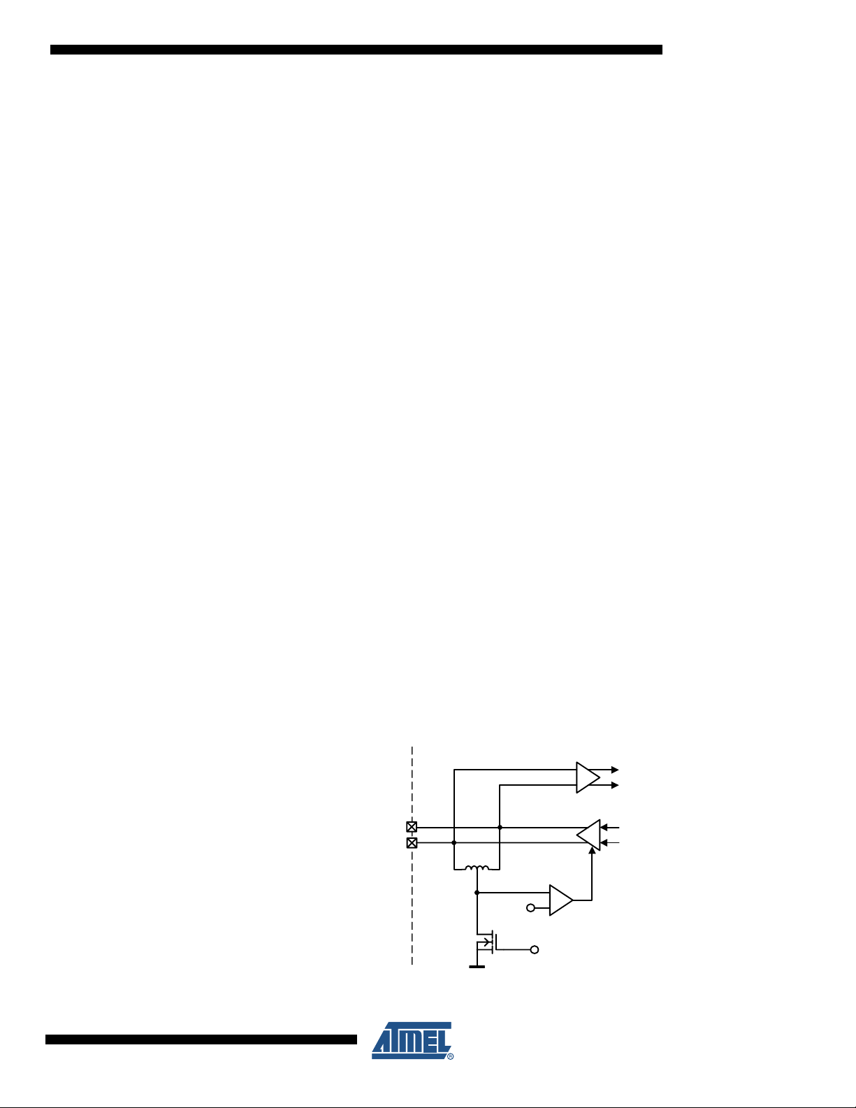
1.2.2 RF Pins RFN, RFP
A differential RF port (RFP/RFN) provides common-mode rejection to suppress the switching
noise of the internal digital signal processing blocks. At board-level, the differential RF layout
ensures high receiver sensitivity by rejecting any spurious emissions originated from other digital
ICs such as a microcontroller.
The RF port is designed for a 100Ω differential load. A DC path between the RF pins is allowed.
A DC path to ground or supply voltage is not allowed. Therefore, when connecting an RF-load
providing a DC path to the power supply or ground, AC-coupling is required as indicated in Table
1-2 on page 6.
A simplified schematic of the RF front end is shown in Figure 1-2 on page 5.
Figure 1-2. Simplified RF Front-end Schematic
AT86RF231PCB
LNA
RFP
RFN
RX
PA
TX
8111A–AVR–05/08
M0
0.9V
CM
Feedback
RXTX
5
Page 6

The RF port DC values depend on the operating state, refer to Section 7. “Operating Modes” on
page 33.
In TRX_OFF state, when the analog front-end is disabled (see Section 7.1.2.3 “TRX_OFF -
Clock State” on page 35), the RF pins are pulled to ground, preventing a floating voltage.
In transmit mode, a control loop provides a common-mode voltage of 0.9V. Transistor M0 is off,
allowing the PA to set the common-mode voltage. The common-mode capacitance at each pin
to ground shall be < 30 pF to ensure the stability of this common-mode feedback loop.
In receive mode, the RF port provides a low-impedance path to ground when transistor M0, see
Figure 1-2 on page 5, pulls the inductor center tap to ground. A DC voltage drop of 20 mV
across the on-chip inductor can be measured at the RF pins.
1.2.3 Crystal Oscillator Pins XTAL1, XTAL2
The pin XTAL1 is the input of the reference oscillator amplifier (XOSC), XTAL2 is the output. A
detailed description of the crystal oscillator setup and the related XTAL1/XTAL2 pin configuration can be found in Section 9.6 “Crystal Oscillator (XOSC)” on page 116.
When using an external clock reference signal, XTAL1 shall be used as input pin.
For further details, refer to Section 9.6.3 “External Reference Frequency Setup” on page 117.
1.2.4 Analog Pin Summary
Table 1-2. Analog Pin Behavior - DC values
Pin Values and Conditions Comments
DC level at pins RFP/RFN for various transceiver states
AC coupling is required if an antenna with a DC path to ground is used.
Serial capacitance and capacitance of each pin to ground must be < 30 pF.
DC level at pins XTAL1/XTAL2 for various transceiver states
Parasitic capacitance (C
load capacitance to the crystal.
DC level at pin DVDD for various transceiver states
Supply pins (voltage regulator output) for the digital 1.8V voltage domain,
recommended bypass capacitor 1 µF.
DC level at pin AVDD for various transceiver states
Supply pin (voltage regulator output) for the analog 1.8V voltage domain,
recommended bypass capacitor 1 µF.
RFP/RFN
XTAL1/ XTAL2
DVD D
AVD D
VDC = 0.9V (BUSY_TX)
VDC = 20 mV (receive states)
= 0 mV (otherwise)
V
DC
= 0.9V at both pins
V
DC
C
= 3 pF
PA R
= 1.8V (all states, except SLEEP)
V
DC
= 0 mV (otherwise)
V
DC
VDC = 1.8V (all states, except P_ON,
SLEEP, RESET, and TRX_OFF)
= 0 mV (otherwise)
V
DC
) of the pins must be considered as additional
PA R
6
AT86RF231
8111A–AVR–05/08
Page 7
AT86RF231
1.3 Digital Pins
The AT86RF231 provides a digital microcontroller interface. The interface comprises a slave
SPI (/SEL, SCLK, MOSI and MISO) and additional control signals (CLKM, IRQ, SLP_TR, /RST
and DIG2). The microcontroller interface is described in detail in Section 6. “Microcontroller
Interface” on page 16.
Additional digital output signals DIG1...DIG4 are provided to control external blocks, i.e. for
Antenna Diversity RF switch control or as an RX/TX Indicator, see Section 11.4 “Antenna Diver-
sity” on page 142 and Section 11.5 “RX/TX Indicator” on page 147. After reset, these pins are
pulled-down to digital ground (DIG1/DIG2) or analog ground (DIG3/DIG4).
1.3.1 Driver Strength Settings
The driver strength of all digital output pins (MISO, IRQ, DIG1, DIG2, DIG3, DIG4) and CLKM
pin can be configured using register 0x03 (TRX_CTRL_0), see Table 1-3 on page 7.
Table 1-3. Digital Output Driver Configuration
Pins Default Driver Strength Recommendation/Comment
MISO, IRQ, DIG1,....., DIG4 2 mA Adjustable to 2 mA, 4 mA, 6 mA and 8 mA
CLKM 4 mA Adjustable to 2 mA, 4 mA, 6 mA and 8 mA
The capacitive load should be as small as possible as, not larger than 50 pF when using the
2 mA minimum driver strength setting. Generally, the output driver strength should be adjusted
to the lowest possible value in order to keep the current consumption and the emission of digital
signal harmonics low.
1.3.2 Pull-Up and Pull-Down Configuration
Pulling resistors are internally connected to all digital input pins in radio transceiver state P_ON,
see Section 7.1.2.1 “P_ON - Power-On after VDD” on page 34. Table 1-4 on page 7 summarizes
the pull-up and pull-down configuration.
Table 1-4. Pull-Up / Pull-Down Configuration of Digital Input Pins in P_ON State
Pins H pull-up, L pull-down
/RST H
/SEL H
SCLK L
MOSI L
SLP_TR L
In all other states, there are no pull-up or pull-down resistors connected to any of the digital input
pins. In RESET state, the pull-up or pull-down resistors are not enabled.
ˆ
=
ˆ
=
8111A–AVR–05/08
7
Page 8
1.3.3 Register Description Register 0x03 (TRX_CTRL_0):
The TRX_CTRL_0 register controls the drive current of the digital output pads and the CLKM
clock rate.
Bit 7 6 5 4 3 2 1 0
PAD_IO PAD_IO_CLKM CLKM_SHA_SEL CLKM_CTRL TRX_CTRL_0
Read/Write R/W R/W R/W R/W R/W R/W R/W R/W
Initial Value 0 0 0 1 1 0 0 1
• Bit [7:6] - PAD_IO
The register bits set the output driver current of all digital output pads, except CLKM.
Table 1-5. Digital Output Driver Strength
Register Bit Value Description
PA D_ I O 0
Note: 1. Reset values of register bits are underlined characterized in the document.
(1)
14 mA
26 mA
38 mA
2 mA
• Bit [5:6] - PAD_IO_CLKM
The register bits set the output driver current of pin CLKM. Refer also to Section 9.6 “Crystal
Oscillator (XOSC)” on page 116.
Table 1-6. CLKM Driver Strength
Register Bit Value Description
PAD_IO_CLKM 0 2 mA
1 4 mA
26 mA
38 mA
• Bit 3 - CLKM_SHA_SEL
Refer to Section 9.6 “Crystal Oscillator (XOSC)” on page 116.
• Bit [2:0] - CLKM_CTRL
Refer to Section 9.6 “Crystal Oscillator (XOSC)” on page 116.
8
AT86RF231
8111A–AVR–05/08
Page 9

2. Disclaimer
3. Overview
AT86RF231
Typical values contained in this datasheet are based on simulations and testing. Min and Max
values are available when the radio transceiver has been fully characterized.
The AT86RF231 is a feature rich, low-power 2.4 GHz radio transceiver designed for industrial
and consumer ZigBee/IEEE 802.15.4 and high data rate 2.4 GHz ISM band applications. The
radio transceiver is a true SPI-to-antenna solution. All RF-critical components except the
antenna, crystal and de-coupling capacitors are integrated on-chip. Therefore, the AT86RF231
is particularly suitable for applications like:
• 2.4 GHz IEEE 802.15.4 and ZigBee systems
• Wireless sensor networks
• Industrial Control
• Residential and commercial automation
• Health care
• Consumer electronics
• PC peripherals
The AT86RF231 can be operated by using an external microcontroller like Atmel's AVR microcontrollers. A comprehensive software programming description can be found in reference [6],
AT86RF231 Software Programming Model.
8111A–AVR–05/08
9
Page 10
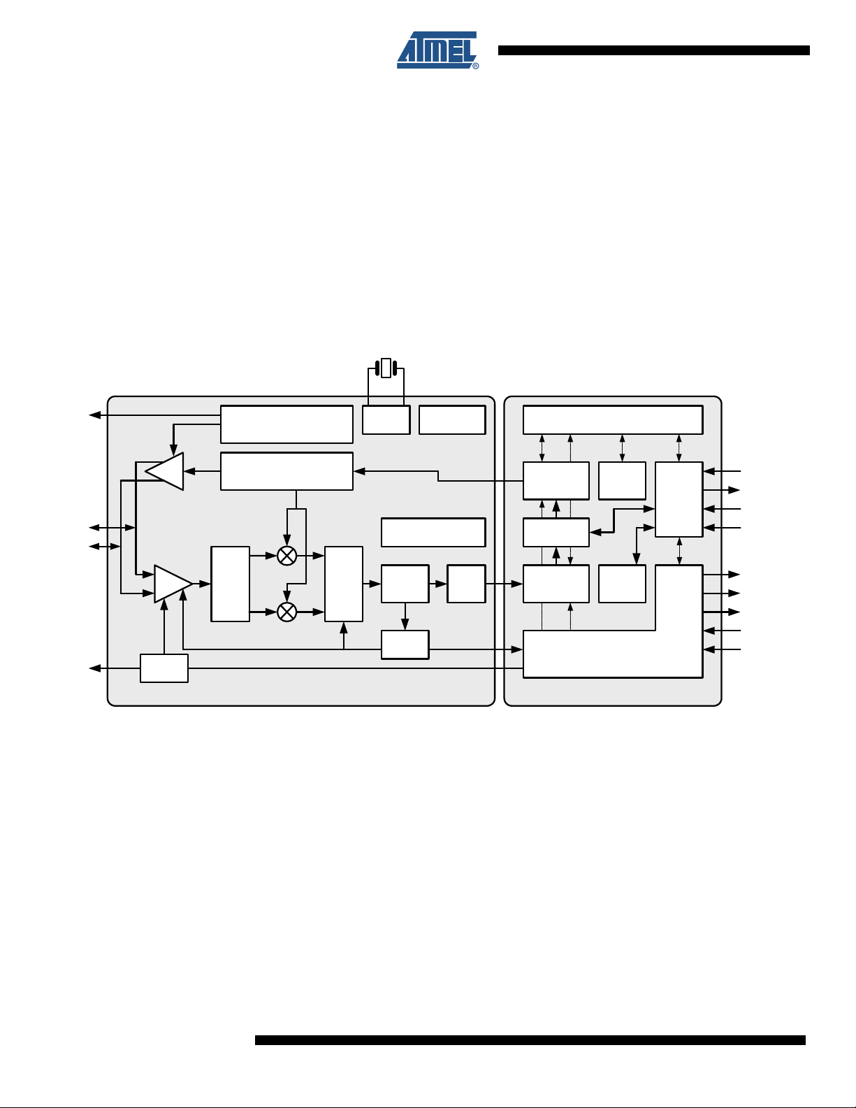
4. General Circuit Description
This single-chip radio transceiver provides a complete radio transceiver interface between an
antenna and a microcontroller. It comprises the analog radio, digital modulation and demodulation including time and frequency synchronization and data buffering. The number of external
components is minimized such that only the antenna, the crystal and decoupling capacitors are
required. The bidirectional differential antenna pins (RFP, RFN) are used for transmission and
reception, thus no external antenna switch is needed.
The AT86RF231 block diagram is shown in Figure 4-1 on page 10.
Figure 4-1. AT86RF231 Block Diagram
DIG3/4
RFP
RFN
DIG1/2
XTAL1
ext. PA and Power
Control
PLL PA
LNA
AD
Analog Domain Digital Domain
PPF BPF Limiter ADC
Antenna Diversity
XOSC
XTAL2
AVREG
TX Data
FTN, BATMON
AGC
Configuration Register s
TX BBP
Frame
Buffer
RX BBP
RSSI
Control Logic
The received RF signal at pins RFN and RFP is differentially fed through the low-noise amplifier
(LNA) to the RF filter (PPF) to generate a complex signal, driving the integrated channel filter
(BPF). The limiting amplifier provides sufficient gain to drive the succeeding analog-to-digital
converter (ADC) and generates a digital RSSI signal. The ADC output signal is sampled by the
digital base band receiver (RX BBP).
DVREG
AES
SPI
(Slave)
/SEL
MISO
MOSI
SCLK
IRQ
CLKM
DIG2
/RST
SLP_TR
10
The transmit modulation scheme is offset-QPSK (O-QPSK) with half-sine pulse shaping and 32length block coding (spreading) according to [1] and [2]. The modulation signal is generated in
the digital transmitter (TX BBP) and applied to the fractional-N frequency synthesis (PLL), to
ensure the coherent phase modulation required for demodulation of O-QPSK signals. The frequency-modulated signal is fed to the power amplifier (PA).
A differential pin pair DIG3/DIG4 can be enabled to control an external RF front-end.
Two on-chip low-dropout voltage regulators (A|DVREG) provide the analog and digital 1.8V
supply.
AT86RF231
8111A–AVR–05/08
Page 11

AT86RF231
An internal 128-byte RAM for RX and TX (Frame Buffer) buffers the data to be transmitted or the
received data.
The configuration of the AT86RF231, reading and writing of Frame Buffer is controlled by the
SPI interface and additional control lines.
The AT86RF231 further contains comprehensive hardware-MAC support (Extended Operating
Mode) and a security engine (AES) to improve the overall system power efficiency and timing.
The stand-alone 128-bit AES engine can be accessed in parallel to all PHY operational transactions and states using the SPI interface, except during SLEEP state.
For applications not necessarily targeting IEEE 802.15.4 compliant networks, the radio transceiver also supports alternative data rates up to 2 Mb/s.
For long-range applications or to improve the reliability of an RF connection the RF performance
can further be improved by using an external RF front-end or Antenna Diversity. Both operation
modes are supported by the AT86RF231 with dedicated control pins without the interaction of
the microcontroller.
Additional features of the Extended Feature Set, see Section 11. “AT86RF231 Extended Fea-
ture Set” on page 128, are provided to simplify the interaction between radio transceiver and
microcontroller.
8111A–AVR–05/08
11
Page 12
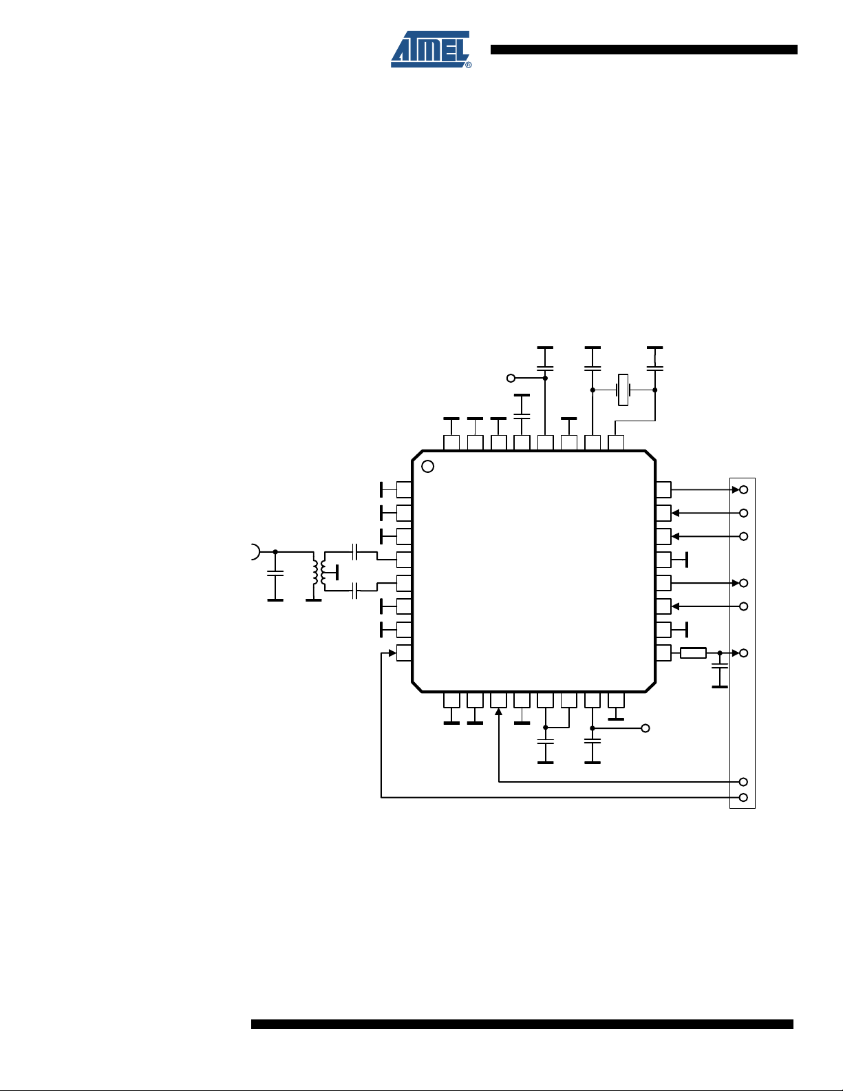
5. Application Circuits
5.1 Basic Application Schematic
A basic application schematic of the AT86RF231 with a single-ended RF connector is shown in
Figure 5-1 on page 12. The 50Ω single-ended RF input is transformed to the 100Ω differential
RF port impedance using balun B1. The capacitors C1 and C2 provide AC coupling of the RF
input to the RF port, capacitor C4 improve matching.
Figure 5-1. Basic Application Schematic
RF
C4
B1
C1
C2
1
2
3
4
5
6
7
8
DIG3
DIG4
AVSS
RFP
RFN
AVSS
DVSS
/RST
9
AVSS
DIG1
AVSS
DIG2
10 11
CB2
V
DD
CB1
AVSS
AVDD
AT86RF231
SLP_TR
DVSS
12
CX1 CX2
EVDD
DVDD
13 14
CB3 CB4
AVSS
DVDD
15 16
XTAL1
DEVDD
XTAL
2526272829303132
XTAL2
/SEL
MOSI
DVSS
MISO
SCLK
DVSS
CLKM
DVSS
IRQ
24
23
22
21
20
19
18
17
V
Digital Interface
R1
C3
DD
12
The power supply decoupling capacitors (CB2, CB4) are connected to the external analog supply pin (EVDD, pin 28) and external digital supply pin (DEVDD, pin 15). Capacitors CB1 and
CB3 are bypass capacitors for the integrated analog and digital voltage regulators to ensure stable operation. All decoupling and bypass capacitors should be placed as close as possible to the
pins and should have a low-resistance and low-inductance connection to ground to achieve the
best performance.
The crystal (XTAL), the two load capacitors (CX1, CX2), and the internal circuitry connected to
pins XTAL1 and XTAL2 form the crystal oscillator. To achieve the best accuracy and stability of
AT86RF231
8111A–AVR–05/08
Page 13

AT86RF231
the reference frequency, large parasitic capacitances should be avoided. Crystal lines should be
routed as short as possible and not in proximity of digital I/O signals. This is especially required
for the High Data Rate Modes, refer to Section 11.3 “High Data Rate Modes” on page 137.
Crosstalk from digital signals on the crystal pins or the RF pins can degrade the system performance. Therefore, a low-pass filter (C3, R1) is placed close to the CLKM output pin to reduce
the emission of CLKM signal harmonics. This is not needed if the CLKM pin is not used as a
microcontroller clock source. In that case, the output should be turned off during device
initialization.
The ground plane of the application board should be separated into four independent fragments,
the analog, the digital, the antenna and the XTAL ground plane. The exposed paddle shall act as
the reference point of the individual grounds.
Table 5-1. Example Bill of Materials (BoM) for Basic Application Schematic
Designator Description Value Manufacture Part Number Comment
B1 SMD balun 2.4 GHz Wuerth 748421245
CB1
CB3
CB2
CB4
CX1, CX2 Crystal load capacitor 12 pF
C3
C4 RF matching 0.47 pF Johnstech
R1
XTAL Crystal
LDO VREG
bypass capacitor
Power Supply decoupling
CLKM low-pass
filter capacitor
CLKM low-pass
filter resistor
1 µF
2.2 pF
680Ω Designed for f
CX-4025 16 MHz
SX-4025 16 MHz
AVX
Murata
AVX
Murata
Epcos
Epcos
AVX
AVX
Murata
ACAL Taitjen
Siward
0603YD105KAT2A
GRM188R61C105KA12D
06035A120JA
GRP1886C1H120JA01
B37930
B37920
06035A220JAT2A
06035A229DA
GRP1886C1H2R0DA01
XWBBPL-F-1
A207-011
X5R
(0603)
COG
(0603)
COG 5%
(0402 or 0603)
COG
(0603)
Designed for f
10% 16V
5%
50VC1, C2 RF coupling capacitor 22 pF
±0.5 pF
=1 MHz
CLKM
=1 MHz
CLKM
8111A–AVR–05/08
13
Page 14
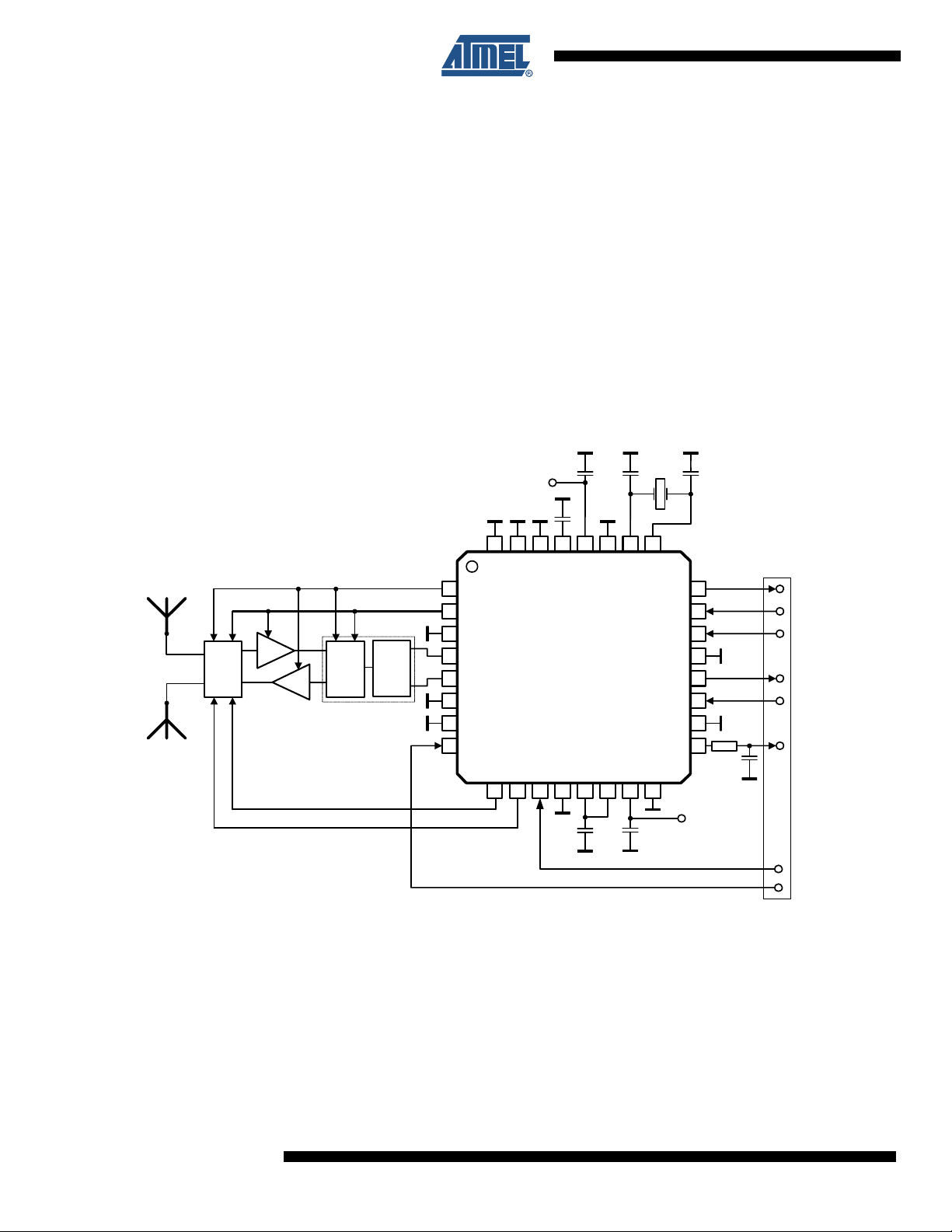
5.2 Extended Feature Set Application Schematic
The AT86RF231 supports additional features like:
•
Security Module (AES) see Section 11.1
•
High Data Rate Mode see Section 11.3
•
Antenna Diversity uses pins DIG1/2 see Section 11.4
•
RX/TX indicator uses pins DIG3/4 see Section 11.5
•
RX Frame Time Stamp uses pin DIG2 see Section 11.6
An extended feature set application schematic illustrating the use of the AT86RF231 Extended
Feature Set, see Section 11. “AT86RF231 Extended Feature Set” on page 128, is shown in Fig-
ure 5-2 on page 14. Although this example shows all additional hardware features combined, it
is possible to use all features separately or in various combinations.
Figure 5-2. Extended Feature Application Schematic
CX1 CX2
CB2
V
DD
CB1
XTAL
ANT0
ANT1
SW2
2526
2728
AVSS
XTAL2
XTAL1
DVDD
DEVDD
IRQ
/SEL
MOSI
DVSS
MISO
SCLK
DVSS
CLKM
DVSS
24
23
22
21
20
19
18
R1
17
C3
V
DD
Digital Interface
RF-
2930
3132
AVSS
AVSS
1
2
N2
LNA
Switch
PA
N1
RF-
Balun
Switch
B1SW1
3
4
5
6
7
8
AVSS
DIG3
DIG4
AVSS
RFP
RFN
AVSS
DVSS
/RST
DIG1
9 10111213141516
AT86RF231
DIG2
SLP_TR
AVDD
DVSS
EVDD
DVDD
CB3 CB4
In this example, a balun (B1) transforms the differential RF signal at the radio transceiver RF
pins (RFP/RFN) to a single ended RF signal, similar to the Basic Application Schematic; refer to
Figure 5-1 on page 12. The RF-Switches (SW1, SW2) separate between receive and transmit
path in an external RF front-end.
14
These switches are controlled by the RX/TX Indicator, represented by the differential pin pair
DIG3/DIG4, refer to Section 11.5 “RX/TX Indicator” on page 147.
During receive the radio transceiver searches for the most reliable RF signal path using the
Antenna Diversity algorithm. One antenna is selected (SW2) by the Antenna Diversity RF switch
AT86RF231
8111A–AVR–05/08
Page 15

AT86RF231
control pins DIG1/DIG2, the RF signal is amplified by an optional low-noise amplifier (N2) and
fed to the radio transceiver using the second RX/TX switch (SW1).
During transmit the AT86RF231 TX signal is amplified using an external PA (N1) and fed to the
antennas via an RF switch (SW2). In this example RF switch SW2 further supports Antenna
Diversity controlled by the differential pin pair DIG1/DIG2.
The security engine (AES) and High Data Rate Modes do not require specific circuitry to operate. The security engine (AES) has to be configured in advance, for details refer to Section 11.1
“Security Module (AES)” on page 128. The High Data Rate Modes are enabled by register bits
OQPSK_DATA_RATE (register 0x0C, TRX_CTRL_2), for details refer to Section 11.3 “High
Data Rate Modes” on page 137.
8111A–AVR–05/08
15
Page 16
6. Microcontroller Interface
This section describes the AT86RF231 to microcontroller interface. The interface comprises a
slave SPI and additional control signals; see Figure 6-1 on page 16. The SPI timing and protocol
are described below.
Figure 6-1. Microcontroller to AT86RF231 Interface
Microcontroller AT86RF231
/SEL /SEL
MOSI
MISO
SPI - Master
SCLK
GPIO1/CLK
GPIO2/IRQ
GPIO3
GPIO4
SPI
/SEL
MOSI
MISO
SCLK
CLKM
IRQ
SLP_TR
/RST
MOSI
MISO
SCLK
CLKM
IRQ
SLP_TR
/RST
SPI - Slave
DIG2GPIO5 DIG2
Microcontrollers with a master SPI such as Atmel's AVR family interface directly to the
AT86RF231. The SPI is used for register, Frame Buffer, SRAM and AES access. The additional
control signals are connected to the GPIO/IRQ interface of the microcontroller.
Table 6-1 on page 16 introduces the radio transceiver I/O signals and their functionality.
Table 6-1. Signal Description of Microcontroller Interface
16
Signal Description
/SEL SPI select signal, active low
MOSI SPI data (master output slave input) signal
MISO SPI data (master input slave output) signal
SCLK SPI clock signal
CLKM Clock output, refer to Section 9.6.4 usable as:
-microcontroller clock source
-high precision timing reference
-MAC timer reference
IRQ Interrupt request signal, further used as:
-Frame Buffer Empty Indicator, refer to Section 11.7
AT86RF231
8111A–AVR–05/08
Page 17
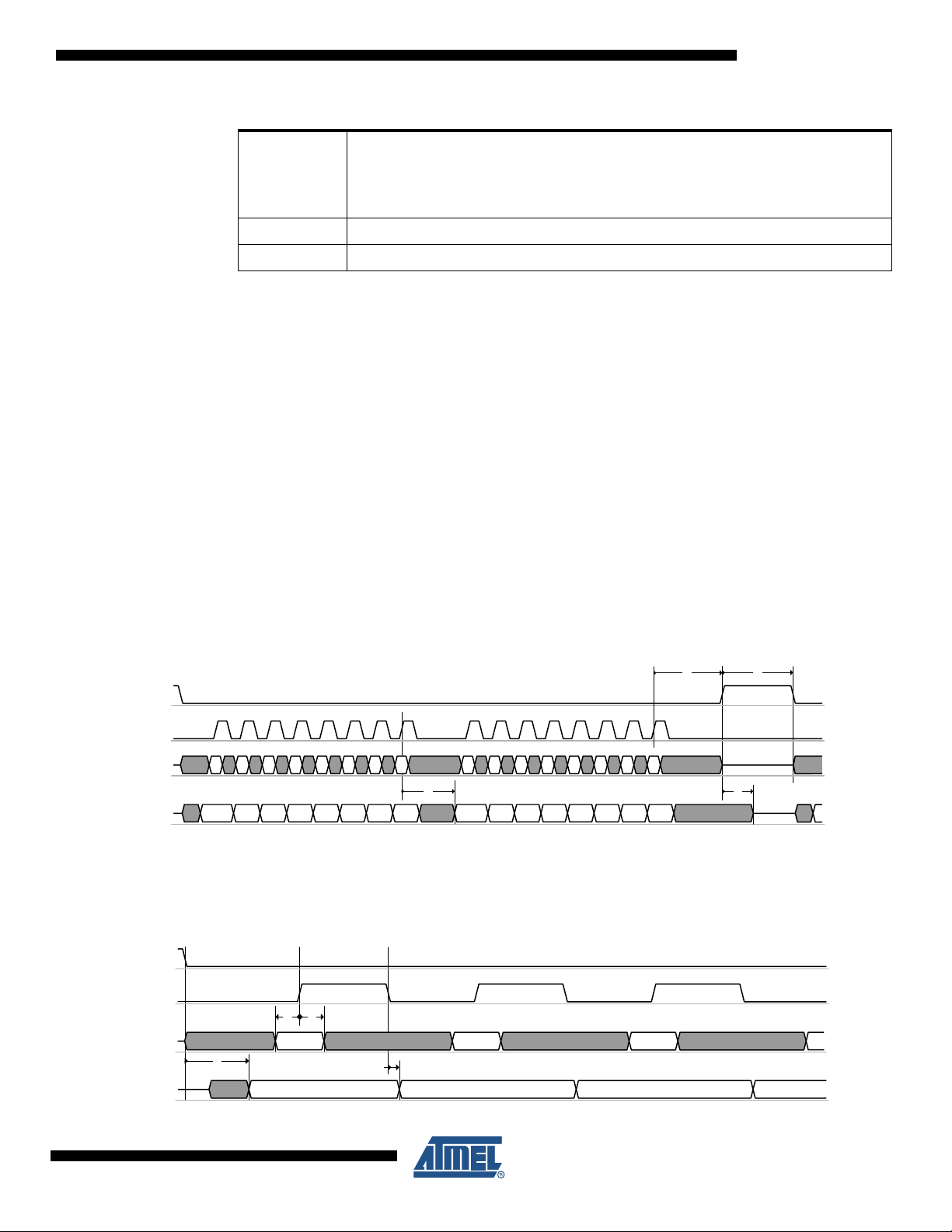
Table 6-1. Signal Description of Microcontroller Interface (Continued)
SLP_TR Multipurpose control signal (functionality is state dependent, see Section 6.5):
/RST AT86RF231 reset signal, active low
DIG2 Optional, IRQ_2 (RX_START) for RX Frame Time Stamping, see Section 11.6
6.1 SPI Timing Description
Pin 17 (CLKM) can be used as a microcontroller master clock source. If the microcontroller
derives the SPI master clock (SCLK) directly from CLKM, the SPI operates in synchronous
mode, otherwise in asynchronous mode.
In synchronous mode, the maximum SCLK frequency is 8 MHz.
In asynchronous mode, the maximum SCLK frequency is limited to 7.5 MHz. The signal at pin
CLKM is not required to derive SCLK and may be disabled to reduce power consumption and
spurious emissions.
AT86RF231
-Sleep/Wakeup enable/disable SLEEP state
-TX start BUSY_TX_(ARET) state
-disable/enable CLKM RX_(AACK)_ON state
Figure 6-2 on page 17 and Figure 6-3 on page 17 illustrate the SPI timing and introduces its
parameters. The corresponding timing parameter definitions t
“Digital Interface Timing Characteristics” on page 157.
Figure 6-2. SPI Timing, Global Map and Definition of Timing Parameters t
/SEL
SCLK
MOSI
MISO
Figure 6-3. SPI Timing, Detailed Drawing of Timing Parameter t1 to t
/SEL
67 5 4 3 2 1 0 67 5 4 3 2 1 0
t
5
Bit 6 Bit 5 Bit 3 Bit 2 Bit 1 Bit 0Bit 4 Bit 6 Bit 5 Bit 3 Bit 2 Bit 1 Bit 0Bit 4Bit 7
Bit 7
4
, t6, t8 and t
5
- t9 are defined in Section 12.4
1
9
t
9
t
8
t
6
SCLK
MOSI
MISO
8111A–AVR–05/08
t4t
3
Bit 7 Bit 6 Bit 5
t
1
Bit 7 Bit 6
t
2
Bit 5
17
Page 18

The SPI is based on a byte-oriented protocol and is always a bidirectional communication
between master and slave. The SPI master starts the transfer by asserting /SEL = L. Then the
master generates eight SPI clock cycles to transfer one byte to the radio transceiver (via MOSI).
At the same time, the slave transmits one byte to the master (via MISO). When the master wants
to receive one byte of data from the slave it must also transmit one byte to the slave. All bytes
are transferred with MSB first. An SPI transaction is finished by releasing /SEL = H.
An SPI register access consists of two bytes, a Frame Buffer or SRAM access of at least two or
more bytes as described in Section 6.2 “SPI Protocol” on page 19.
/SEL = L enables the MISO output driver of the AT86RF231. The MSB of MISO is valid after t1
(see Section 12.4 “Digital Interface Timing Characteristics” on page 157 parameter 12.4.3) and
is updated at each falling edge of SCLK. If the driver is disabled, there is no internal pull-up
resistor connected to it. Driving the appropriate signal level must be ensured by the master
device or an external pull-up resistor. Note, when both /SEL and /RST are active, the MISO output driver is also enabled.
Referring to Figure 6-2 on page 17 and Figure 6-3 on page 17 MOSI is sampled at the rising
edge of the SCLK signal and the output is set at the falling edge of SCLK. The signal must be
stable before and after the rising edge of SCLK as specified by t
“Digital Interface Timing Characteristics” on page 157 parameters 12.4.5 and 12.4.6.
This SPI operational mode is commonly known as "SPI mode 0".
and t4, refer to Section 12.4
3
18
AT86RF231
8111A–AVR–05/08
Page 19
AT86RF231
6.2 SPI Protocol
Each SPI sequence starts with transferring a command byte from the SPI master via MOSI (see
Table 6-2 on page 19) with MSB first. This command byte defines the SPI access mode and
additional mode-dependent information.
Table 6-2. SPI Command Byte definition
Bit 7 Bit 6 Bit 5 Bit 4 Bit 3 Bit 2 Bit 1 Bit 0 Access Mode Access Type
1 0 Register address [5:0]
Register access
1 1 Register address [5:0] Write access
Read access
001 Reserved
Frame Buffer access
0 1 1 Reserved Write access
000 Reserved
SRAM access
0 1 0 Reserved Write access
Read access
Read access
Each SPI transfer returns bytes back to the SPI master on MISO. The content of the first byte
(see value "PHY_STATUS" in Figure 6-4 on page 19 to Figure 6-14 on page 23) is set to zero
after reset. To transfer status information of the radio transceiver to the microcontroller, the content of the first byte can be configured with register bits SPI_CMD_MODE (register 0x04,
TRX_CTRL_1). For details, refer to Section 6.3.1 “Register Description - SPI Control” on page
24.
In Figure 6-4 on page 19 to Figure 6-14 on page 23 and the following chapters logic values
stated with XX on MOSI are ignored by the radio transceiver, but need to have a valid logic level.
Return values on MISO stated as XX shall be ignored by the microcontroller.
The different access modes are described within the following sections.
6.2.1 Register Access Mode
A register access mode is a two-byte read/write operation initiated by /SEL = L. The first transferred byte on MOSI is the command byte including an identifier bit (bit7 = 1), a read/write select
bit (bit 6), and a 6-bit register address.
On read access, the content of the selected register address is returned in the second byte on
MISO (see Figure 6-4 on page 19).
8111A–AVR–05/08
Figure 6-4. Packet Structure - Register Read Access
byte 1 (command byte) byte 2 (data byte)
1 ADDRESS[5:0]0 XXMOSI
PHY_STATUS
Note: 1. Each SPI access can be configured to return radio controller status information
(PHY_STATUS) on MISO, for details refer to Section 6.3 “Radio Transceiver Status informa-
tion” on page 24.
(1)
READ DATA[7:0]MISO
On write access, the second byte transferred on MOSI contains the write data to the selected
address (see Figure 6-6 on page 20).
19
Page 20
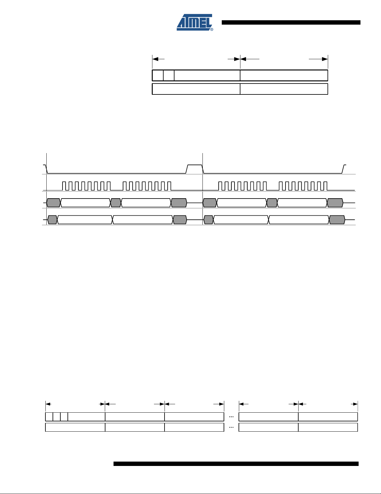
Figure 6-5. Packet Structure - Register Write Access
byte 1 (command byte) byte 2 (data byte)
1 ADDRESS[5:0]1 WRITE DATA[7:0]MOSI
PHY_STATUS XXMISO
Each register access must be terminated by setting /SEL = H.
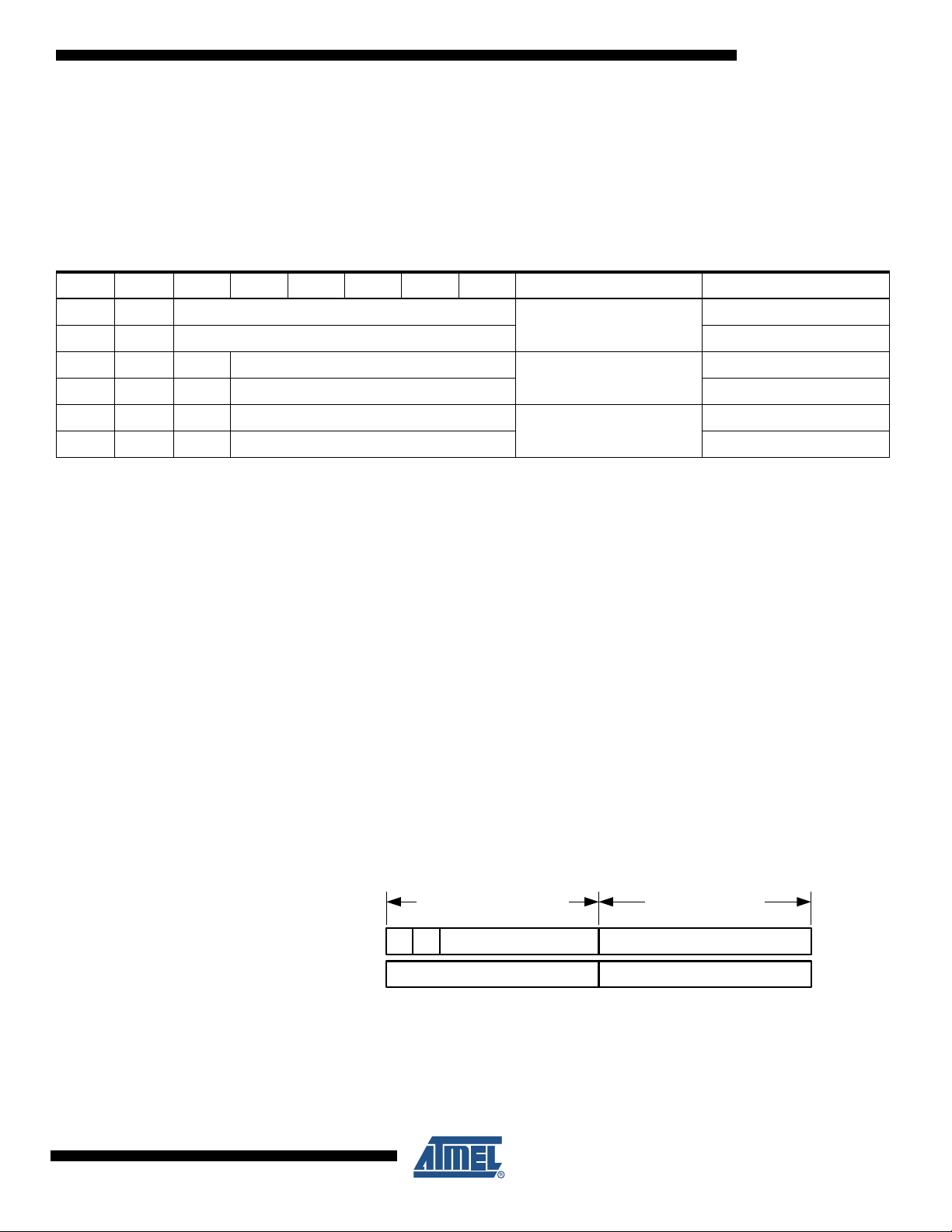
Figure 6-6 on page 20 illustrates a typical SPI sequence for a register access sequence for write
and read respectively.
Figure 6-6. Example SPI Sequence - Register Access Mode
Register Write Access Register Read Access
/SEL
SCLK
MOSI
MISO
WRITE COMMAND WRITE DATA READ COMMAND XX
PHY_STATUS XX PHY_STATUS READ DATA
6.2.2 Frame Buffer Access Mode
The 128 byte Frame Buffer can hold the PHY service data unit (PSDU) data of one
IEEE 802.15.4 compliant RX or one TX frame of maximum length at a time. A detailed description of the Frame Buffer can be found in Section 9.3 “Frame Buffer” on page 107. An introduction
to the IEEE 802.15.4 frame format can be found in Section 8.1 “Introduction - IEEE 802.15.4 -
2006 Frame Format” on page 79.
Frame Buffer read and write accesses are used to read or write frame data (PSDU and additional information) from or to the Frame Buffer. Each access starts with /SEL = L followed by a
command byte on MOSI. If this byte indicates a frame read or write access, the next byte
PHR[7:0] indicates the frame length followed by the PSDU data, see Figure 6-7 on page 20 and
Figure 6-8 on page 21.
On Frame Buffer read access, PHY header (PHR) and PSDU are transferred via MISO starting
with the second byte. After the PSDU data, one more byte is transferred containing the link quality indication (LQI) value of the received frame, for details refer to Section 8.6 “Link Quality
Indication (LQI)” on page 99. Figure 6-7 on page 20 illustrates the packet structure of a Frame
Buffer read access.
Figure 6-7. Packet Structure - Frame Read Access
20
byte 1 (command byte)
0 reserved[5:0]0MOSI
1 XX
PHY_STATUSMISO
AT86RF231
byte 2 (data byte)
PHR[7:0]
byte 3 (data byte)
XX
PSDU[7:0]
byte n-1 (data byte)
XX
PSDU[7:0]
byte n (data byte)
XX
LQI[7:0]
8111A–AVR–05/08
Page 21
Note, the Frame Buffer read access can be terminated at any time without any consequences by
setting /SEL = H, e.g. after reading the PHR byte only.
On Frame Buffer write access the second byte transferred on MOSI contains the frame length
(PHR field) followed by the payload data (PSDU) as shown by Figure 6-8 on page 21.
Figure 6-8. Packet Structure - Frame Write Access
AT86RF231
byte 1 (command byte)
0 reserved[5:0]1MOSI
1 PHR[7:0]
PHY_STATUSMISO
The number of bytes n for one frame access is calculated as follows:
• Read Access:
• Write Access:
The maximum value of frame_length is 127 bytes. That means that n ≤ 130 for Frame Buffer
read and n ≤ 129 for Frame Buffer write accesses.
Each read or write of a data byte increments automatically the address counter of the Frame
Buffer until the access is terminated by setting /SEL = H. A Frame Buffer read access may be
terminated (/SEL = H) at any time without affecting the Frame Buffer content. Another Frame
Buffer read operation starts again at the PHR field.
The content of the Frame Buffer is only overwritten by a new received frame or a Frame Buffer
write access.
byte 2 (data byte)
XX
byte 3 (data byte)
PSDU[7:0]
XX
byte n-1 (data byte)
PSDU[7:0]
XX
n = 3 + frame_length
[PHY_STATUS, PHR byte, PSDU data, and LQI byte]
n = 2 + frame_length
[command byte, PHR byte, and PSDU data]
byte n (data byte)
PSDU[7:0]
XX
Figure 6-9 on page 21 and Figure 6-10 on page 22 illustrate an example SPI sequence of a
Frame Buffer access to read and write a frame with 4-byte PSDU respectively.
Figure 6-9. Example SPI Sequence - Frame Buffer Read of a Frame with 4-byte PSDU
/SEL
SCLK
MOSI
MISO
8111A–AVR–05/08
COMMAND XX XX XX XX XX
PHY_STATUS PHR PSDU 2PSDU 1 PSDU 4PSDU 3
XX
LQI
21
Page 22
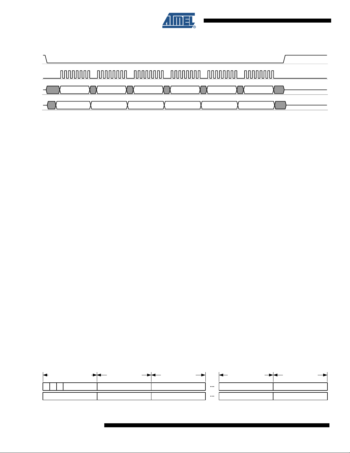
Figure 6-10. Example SPI Sequence - Frame Buffer Write of a Frame with 4 byte PSDU
/SEL
SCLK
MOSI
MISO
COMMAND PHR PSDU 1 PSDU 2 PSDU 3 PSDU 4
PHY_STATUS XX XXXX XXXX
Access violations during a Frame Buffer read or write access are indicated by interrupt IRQ_6
(TRX_UR). For further details, refer to Section 9.3 “Frame Buffer” on page 107.
Notes
• The Frame Buffer is shared between RX and TX; therefore, the frame data are overwritten by
new incoming frames. If the TX frame data are to be retransmitted, it must be ensured that no
frame was received in the meanwhile.
• To avoid overwriting during receive Dynamic Frame Buffer Protection can be enabled, refer to
Section 11.8 “Dynamic Frame Buffer Protection” on page 154.
• It is not possible to retransmit received frames without a Frame Buffer read and write access
cycle.
• For exceptions, e.g. receiving acknowledgement frames in Extended Operating Mode
(TX_ARET) refer to Section 7.2.4 “TX_ARET_ON - Transmit with Automatic Retry and
CSMA-CA Retry” on page 64.
6.2.3 SRAM Access Mode
The SRAM access mode allows accessing dedicated bytes within the Frame Buffer. This may
reduce the SPI traffic.
The SRAM access mode is useful, for instance, if a transmit frame is already stored in the Frame
Buffer and dedicated bytes (e.g. sequence number, address field) need to be replaced before
retransmitting the frame. Furthermore, it can be used to access only the LQI value after frame
reception. A detailed description of the user accessible frame content can be found in Section
9.3 “Frame Buffer” on page 107.
Each SRAM access starts with /SEL = L. The first transferred byte on MOSI shall be the command byte and must indicate an SRAM access mode according to the definition in Table 6-2 on
page 19. The following byte indicates the start address of the write or read access. The address
space is 0x00 to 0x7F for radio transceiver receive or transmit operations.
On SRAM read access, one or more bytes of read data are transferred on MISO starting with the
third byte of the access sequence (see Figure 6-11 on page 22).
Figure 6-11. Packet Structure - SRAM Read Access
22
byte 1 (command byte)
0 reserved[5:0]0MOSI
0 ADDRESS[7:0]
PHY_STATUSMISO
AT86RF231
byte 2 (address)
XX
byte 3 (data byte)
XX
DATA[7:0]
byte n-1 (data byte)
XX
DATA[7:0]
byte n (data byte)
XX
DATA[7:0]
8111A–AVR–05/08
Page 23
On SRAM write access, one or more bytes of write data are transferred on MOSI starting with
the third byte of the access sequence (see Figure 6-12 on page 23).
On SRAM read or write accesses do not attempt to read or write bytes beyond the SRAM buffer
size.
Figure 6-12. Packet Structure - SRAM Write Access
AT86RF231
byte 1 (command byte)
0 reserved[5:0]1MOSI
0 ADDRESS[7:0]
PHY_STATUSMISO
byte 2 (address)
XX
byte 3 (data byte)
DATA[7:0]
XX
byte n-1 (data byte)
DATA[7:0]
As long as /SEL = L, every subsequent byte read or byte write increments the address counter
of the Frame Buffer until the SRAM access is terminated by /SEL = H.
Figure 6-13 on page 23 and Figure 6-14 on page 23 illustrate an example SPI sequence of a
SRAM access to read and write a data package of 5-byte length respectively.
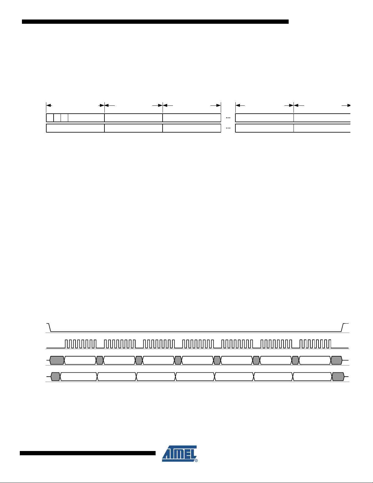
Figure 6-13. Example SPI Sequence - SRAM Read Access of a 5 byte Data Package
/SEL
SCLK
MOSI
MISO
COMMAND ADDRESS XX XX XX XX
PHY_STATUS XX DATA 2DATA 1 DATA 4DATA 3
Figure 6-14. Example SPI Sequence - SRAM Write Access of a 5 byte Data Package
XX
byte n (data byte)
DATA[7:0]
XX
XX
DATA 5
/SEL
SCLK
MOSI
MISO
8111A–AVR–05/08
COMMAND ADDRESS DATA 1 DATA 2 DATA 3 DATA 4
PHY_STATUS XX XXXX XXXX
Notes
• The SRAM access mode is not intended to be used as an alternative to the Frame Buffer
access modes (see Section 6.2.2 “Frame Buffer Access Mode” on page 20).
• If the SRAM access mode is used to read PSDU data, the Frame Buffer contains all PSDU
data except the frame length byte (PHR). The frame length information can be accessed only
using Frame Buffer access.
• Frame Buffer access violations are not indicated by a TRX_UR interrupt when using the
SRAM access mode, for further details refer to Section 9.3.3 “Interrupt Handling” on page
109.
DATA 5
XX
23
Page 24
6.3 Radio Transceiver Status information
Each SPI access can be configured to return status information of the radio transceiver
(PHY_STATUS) to the microcontroller using the first byte of the data transferred via MISO.
The content of the radio transceiver status information can be configured using register bits
SPI_CMD_MODE (register 0x04, TRX_CTRL_1). After reset, the content on the first byte send
on MISO to the microcontroller is set to 0x00.
6.3.1 Register Description - SPI Control Register 0x04 (TRX_CTRL_1):
The TRX_CTRL_1 register is a multi purpose register to control various operating modes and
settings of the radio transceiver.
Bit 7 6 5 4 3 2 1 0
+0x04 PA_EXT_EN IRQ_2_EXT_EN TX_AUTO_CRC_ON RX_BL_CTRL SPI_CMD_MODE IRQ_MASK_MODE IRQ_POLARITY TRX_CTRL_1
Read/Write R/W R/W R/W R/W R/W R/W R/W R/W
Initial Value 0 0 1 0 0 0 0 0
• Bit 7 - PA_EXT_EN
Refer to Section 11.5 “RX/TX Indicator” on page 147.
• Bit 6 - IRQ_2_EXT_EN
Refer to Section 11.6 “RX Frame Time Stamping” on page 150.
• Bit 5 - TX_AUTO_CRC_ON
Refer to Section 8.2 “Frame Check Sequence (FCS)” on page 85.
• Bit 4 - RX_BL_CTRL
Refer to Section 11.7 “Frame Buffer Empty Indicator” on page 152.
• Bit [3:2] - SPI_CMD_MODE
Each SPI transfer returns bytes back to the SPI master. The content of the first byte can be configured using register bits SPI_CMD_MODE. The transfer of the following status information can
be configured as follows:
Table 6-3. Radio Transceiver Status Information - PHY_STATUS
Register Bit Value Description
SPI_CMD_MODE 0
1 monitor TRX_STATUS register; see Section 7.1.5
2 monitor PHY_RSSI register; see Section 8.3
3 monitor IRQ_STATUS register; see Section 6.6
default (empty, all bits 0x00)
• Bit 1 - IRQ_MASK_MODE
Refer to Section 6.6 “Interrupt Logic” on page 29.
24
• Bit 0 - IRQ_POLARITY
Refer to Section 6.6 “Interrupt Logic” on page 29.
AT86RF231
8111A–AVR–05/08
Page 25
6.4 Radio Transceiver Identification
The AT86RF231 can be identified by four registers. One register contains a unique part number
and one register the corresponding version number. Two additional registers contain the JEDEC
manufacture ID.
6.4.1 Register Description - AT86RF231 Identification
Register 0x1C (PART_NUM):
Bit 76543210
+0x1C PART_NUM[7:0] PART_NUM
Read/WriteRRRRRRRR
Reset Value00000011
• Bit [7:0] - PART_NUM
This register contains the radio transceiver part number.
Table 6-4. Radio Transceiver Part Number
Register Bit Value Description
AT86RF231
PA RT _ N UM 3
AT86RF231 part number
Register 0x1D (VERSION_NUM):
Bit 76543210
+0x1D VERSION_NUM[7:0] VERSION_NUM
Read/WriteRRRRRRRR
Reset Value00000010
• Bit [7:0] - VERSION_NUM
This register contains the radio transceiver version number.
Table 6-5. Radio Transceiver Version Number
Register Bit Value Description
VERSION_NUM 2
Revision A
Register 0x1E (MAN_ID_0):
Bit 76543210
+0x1E MAN_ID_0[7:0] MAN_ID_O
Read/WriteRRRRRRRR
Reset Value00011111
8111A–AVR–05/08
• Bit [7:0] - MAN_ID_0
Bits [7:0] of the 32-bit JEDEC manufacturer ID are stored in register bits MAN_ID_0. Bits [15:8]
are stored in register 0x1F (MAN_ID_1). The highest 16 bits of the ID are not stored in registers.
25
Page 26
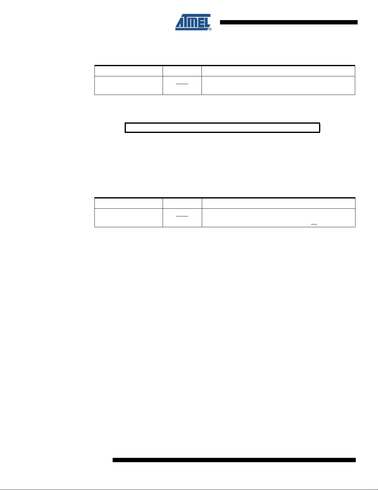
Table 6-6. JEDEC Manufacturer ID - Bits [7:0]
Register Bit Value Description
MAN_ID_0 0x1F
Atmel JEDEC manufacturer ID,
Bits [7:0] of 32 bit manufacturer ID: 00 00 00 1F
Register 0x1F (MAN_ID_1):
Bit 76543210
+0x1F MAN_ID_1[7:0] MAN_ID_1
Read/WriteRRRRRRRR
Reset Value00000000
• Bit [7:0] - MAN_ID_1
Bits [15:8] of the 32-bit JEDEC manufacturer ID are stored in register bits MAN_ID_1. Bits [7:0]
are stored in register 0x1E (MAN_ID_0). The higher 16 bits of the ID are not stored in registers.
Table 6-7. JEDEC Manufacturer ID - Bits [15:8]
Register Bit Value Description
MAN_ID_1 0x00
Atmel JEDEC manufacturer ID,
Bits [15:8] of 32 bit manufacturer ID: 00 00 00 1F
26
AT86RF231
8111A–AVR–05/08
Page 27

AT86RF231
6.5 Sleep/Wake-up and Transmit Signal (SLP_TR)
Pin 11 (SLP_TR) is a multi-functional pin. Its function relates to the current state of the
AT86RF231 and is summarized in Table 6-8 on page 27. The radio transceiver states are
explained in detail Section 7. “Operating Modes” on page 33.
Table 6-8. SLP_TR Multi-functional Pin
Transceiver Status Function Transition Description
PLL_ON TX start Starts frame transmission
TX_ARET_ON TX start Starts TX_ARET transaction
TRX_OFF Sleep Takes the radio transceiver into SLEEP state, CLKM disabled
SLEEP Wakeup Takes the radio transceiver back into TRX_OFF state, level sensitive
RX_ON Disable CLKM Takes the radio transceiver into RX_ON_NOCLK state and disables CLKM
RX_ON_NOCLK Enable CLKM Takes the radio transceiver into RX_ON state and enables CLKM
RX_AACK_ON Disable CLKM
RX_AACK_ON_NOCLK Enable CLKM Takes the radio transceiver into RX_AACK_ON state and enables CLKM
LH⇒
LH⇒
LH⇒
HL⇒
LH⇒
HL⇒
LH⇒
HL⇒
Takes the radio transceiver into RX_AACK_ON_NOCLK state and disables
CLKM
In states PLL_ON and TX_ARET_ON, pin SLP_TR is used as trigger input to initiate a TX transaction. Here pin SLP_TR is sensitive on rising edge only.
After initiating a state change by a rising edge at pin SLP_TR in radio transceiver states
TRX_OFF, RX_ON or RX_AACK_ON, the radio transceiver remains in the new state as long as
the pin is logical high and returns to the preceding state with the falling edge.
SLEEP state
The SLEEP state is used when radio transceiver functionality is not required, and thus the
AT86RF231 can be powered down to reduce the overall power consumption.
A power-down scenario is shown in Figure 6-15 on page 28. When the radio transceiver is in
TRX_OFF state the microcontroller forces the AT86RF231 to SLEEP by setting SLP_TR = H. If
pin 17 (CLKM) provides a clock to the microcontroller this clock is switched off after 35 clock
cycles. This enables a microcontroller in a synchronous system to complete its power-down routine and prevent deadlock situations. The AT86RF231 awakes when the microcontroller
releases pin SLP_TR. This concept provides the lowest possible power consumption.
The CLKM clock frequency settings for 250 kHz and 62.5 kHz are not intended to directly clock
the microcontroller. When using these clock rates, CLKM is turned off immediately when entering SLEEP state.
8111A–AVR–05/08
27
Page 28
Figure 6-15. Sleep and Wake-up Initiated by Asynchronous Microcontroller Timer
SLP_TR
CLKM
t
TR2
35 CLKM clock cycles CLKM off
Note: Timing figure t
refer to section Table 7-1 on page 42.
TR2
async timer elapses
(microcontroller)
RX_ON and RX_AACK_ON states
For synchronous systems, where CLKM is used as a microcontroller clock source and the SPI
master clock (SCLK) is directly derived from CLKM, the AT86RF231 supports an additional
power-down mode for receive operating states (RX_ON and RX_AACK_ON).
If an incoming frame is expected and no other applications are running on the microcontroller, it
can be powered down without missing incoming frames.
This can be achieved by a rising edge on pin SLP_TR that turns off the CLKM. Then the radio
transceiver state changes from RX_ON or RX_AACK_ON (Extended Operating Mode) to
RX_ON_NOCLK or RX_AACK_ON_NOCLK respectively.
In case that a frame is received (e.g. indicated by an IRQ_2 (RX_START) interrupt) the clock
output CLKM is automatically switched on again.
This scenario is shown in Figure 6-16 on page 28. In RX_ON state, the clock at pin 17 (CLKM) is
switched off after 35 clock cycles when setting the pin SLP_TR = H.
The CLKM clock frequency settings for 250 kHz and 62.5 kHz are not intended to directly clock
the microcontroller. When using these clock rates, CLKM is turned off immediately when entering RX_ON_NOCLK and RX_AACK_ON_NOCLK respectively.
In states RX_(AACK)_ON_NOCLK and RX_(AACK)_ON, the radio transceiver current consumptions are equivalent. However, the RX_(AACK)_ON_NOCLK current consumption is
reduced by the current required for driving pin 17 (CLKM).
Figure 6-16. Wake-Up Initiated by Radio Transceiver Interrupt
radio transceiver
IRQ
SLP_TR
CLKM
35 CLKM clock cycles CLKM off
28
AT86RF231
typ. 5 µs
IRQ issued
8111A–AVR–05/08
Page 29

AT86RF231
6.6 Interrupt Logic
6.6.1 Overview
The AT86RF231 differentiates between nine interrupt events (eight physical interrupt registers,
one shared by two functions). Each interrupt is enabled by setting the corresponding bit in the
interrupt mask register 0x0E (IRQ_MASK). Internally, each pending interrupt is stored in a separate bit of the interrupt status register. All interrupt events are OR-combined to a single external
interrupt signal (IRQ, pin 24). If an interrupt is issued (pin IRQ = H), the microcontroller shall read
the interrupt status register 0x0F (IRQ_STATUS) to determine the source of the interrupt. A read
access to this register clears the interrupt status register and thus the IRQ pin, too.
Interrupts are not cleared automatically when the event that caused them vanishes. Exceptions
are IRQ_0 (PLL_LOCK) and IRQ_1 (PLL_UNLOCK) because the occurrence of one clears the
other.
The supported interrupts for the Basic Operating Mode are summarized in Table 6-9 on page
29.
Table 6-9. Interrupt Description in Basic Operating Mode
IRQ Name Description Section
IRQ_7 (BAT_LOW) Indicates a supply voltage below the programmed threshold. Section 9.5.4
IRQ_6 (TRX_UR) Indicates a Frame Buffer access violation. Section 9.3.3
IRQ_5 (AMI) Indicates address matching. Section 7.2.3.5
Multi-functional interrupt:
1. AWAKE_END:
IRQ_4 (CCA_ED_READY)
IRQ_3 (TRX_END)
IRQ_2 (RX_START)
IRQ_1 (PLL_UNLOCK)
IRQ_0 (PLL_LOCK) Indicates PLL lock. Section 9.7.5
• Indicates radio transceiver reached TRX_OFF state after P_ON, RESET, or
SLEEP states.
2. CCA_ED_READY:
• Indicates the end of a CCA or ED measurement.
RX: Indicates the completion of a frame reception.
TX: Indicates the completion of a frame transmission.
Indicates the start of a PSDU reception. The TRX_STATE changes to BUSY_RX,
the PHR is valid to read from Frame Buffer.
Indicates PLL unlock. If the radio transceiver is BUSY_TX / BUSY_TX_ARET
state, the PA is turned off immediately.
Section 7.1.2.3
Section 8.4.4
Section 8.5.4
Section 7.1.3
Section 7.1.3
Section 7.1.3
Section 9.7.5
The interrupt IRQ_4 has two meanings, depending on the current radio transceiver state, refer to
register 0x01 (TRX_STATUS).
After P_ON, SLEEP, or RESET, the radio transceiver issues an interrupt IRQ_4 (AWAKE_END)
when it enters state TRX_OFF.
The second meaning is only valid for receive states. If the microcontroller initiates an energydetect (ED) or clear-channel-assessment (CCA) measurement, the completion of the measurement is indicated by interrupt IRQ_4 (CCA_ED_READY), refer to Section 8.4.4 “Interrupt
Handling” on page 92 and Section 8.5.4 “Interrupt Handling” on page 95 for details.
8111A–AVR–05/08
After P_ON or RESET all interrupts are disabled. During radio transceiver initialization it is recommended to enable IRQ_4 (AWAKE_END) to be notified once the TRX_OFF state is entered.
29
Page 30

Note that AWAKE_END interrupt can usually not be seen when the transceiver enters
TRX_OFF state after RESET, because register 0x0E (IRQ_MASK) is reset to mask all interrupts. In this case, state TRX_OFF is normally entered before the microcontroller could modify
the register.
The interrupt handling in Extended Operating Mode is described in Section 7.2.5 “Interrupt Han-
dling” on page 67.
If register bit IRQ_MASK_MODE (register 0x04, TRX_CTRL_1) is set, an interrupt event can be
read from IRQ_STATUS register even if the interrupt itself is masked. However, in that case no
timing information for this interrupt is provided.
The IRQ pin polarity can be configured with register bit IRQ_POLARITY (register 0x04,
TRX_CTRL_1). The default behavior is active high, which means that pin IRQ = H issues an
interrupt request.
If "Frame Buffer Empty Indicator" is enabled during Frame Buffer read access the IRQ pin has
an alternative functionality, refer to Section 11.7 “Frame Buffer Empty Indicator” on page 152 for
details.
6.6.2 Register Description Register 0x0E (IRQ_MASK):
he IRQ_MASK register is used to enable or disable individual interrupts. An interrupt is enabled
if the corresponding bit is set to 1. All interrupts are disabled after power up sequence (P_ON
state) or reset (RESET state).
Bit 7 6 5 4 3 2 1 0
+0x0E MASK_BAT_LOW MASK_TRX_UR MASK_AMI MA SK_CCA_ED_READY MASK_TRX_ END
Read/Write R/W R/W R/W R/W R/W R/W R/W R/W
Reset Value 0 0 0 0 0 0 0 0
MASK_RX_START MASK_PLL_UNLOCK MASK_PLL_LOCK IRQ_MASK
If an interrupt is enabled it is recommended to read the interrupt status register 0x0F
(IRQ_STATUS) first to clear the history.
Register 0x0F (IRQ_STATUS):
The IRQ_STATUS register contains the status of the pending interrupt requests.
Bit 7 6 5 4 3 2 1 0
+0x0F BAT_LOW TRX_UR AMI CCA_ED_READY TRX_END RX_START PLL_UNLOCK PLL_LOCK IRQ_STATUS
Read/Write R R R R R R R R
Initial Value 0 0 0 0 0 0 0 0
By reading the register after an interrupt is signaled at pin 24 (IRQ) the source of the issued
interrupt can be identified. A read access to this register resets all interrupt bits, and so clears
the IRQ_STATUS register.
If register bit IRQ_MASK_MODE (register 0x04, TRX_CTRL_1) is set, an interrupt event can be
read from IRQ_STATUS register even if the interrupt itself is masked. However in that case no
timing information for this interrupt is provided.
If register bit IRQ_MASK_MODE is set, it is recommended to read the interrupt status register
0x0F (IRQ_STATUS) first to clear the history.
30
AT86RF231
8111A–AVR–05/08
Page 31

AT86RF231
Register 0x04 (TRX_CTRL_1):
The TRX_CTRL_1 register is a multi purpose register to control various operating modes and
settings of the radio transceiver.
Bit 7 6 5 4 3 2 1 0
+0x04 PA_EXT_EN IRQ_2_EXT_EN TX_AUTO_CRC_ON RX_BL_CTRL SPI_CMD_MODE IRQ_MASK_MODE IRQ_POLARITY TRX_CTRL_1
Read/Write R/W R/W R/W R/W R/W R/W R/W R/W
Reset Value 0 0 1 0 0 0 0 0
• Bit 7 - PA_EXT_EN
Refer to Section 11.5 “RX/TX Indicator” on page 147.
• Bit 6 - IRQ_2_EXT_EN
The timing of a received frame can be determined by a separate pin. If register bit
IRQ_2_EXT_EN is set to 1, the reception of a PHR is directly issued on pin 10 (DIG2), similar to
interrupt IRQ_2 (RX_START). Note that this pin is also active even if the corresponding interrupt
event IRQ_2 (RX_START) mask bit in register 0x0E (IRQ_MASK) is set to 0. The pin remains at
high level until the end of the frame receive procedure.
For further details refer to Section 11.6 “RX Frame Time Stamping” on page 150.
• Bit 5 - TX_AUTO_CRC_ON
Refer to Section 8.2 “Frame Check Sequence (FCS)” on page 85.
• Bit 4 - RX_BL_CTRL
Refer to Section 11.7 “Frame Buffer Empty Indicator” on page 152.
• Bit [3:2] - SPI_CMD_MODE
Refer to Section 6.3 “Radio Transceiver Status information” on page 24.
• Bit 1 - IRQ_MASK_MODE
The AT86RF231 supports polling of interrupt events. Interrupt polling can be enabled by register
bit IRQ_MASK_MODE. Even if an interrupt request is masked by the corresponding bit in register 0x0E (IRQ_MASK), the event is indicated in register 0x0F (IRQ_STATUS).
Table 6-10. Interrupt Polling Configuration
Register Bit Value Description
IRQ_MASK_MODE 0
1 Interrupt polling enabled
Interrupt polling disabled
8111A–AVR–05/08
31
Page 32

• Bit 0 - IRQ_POLARITY
The default polarity of the IRQ pin is active high. The polarity can be configured to active low via
register bit IRQ_POLARITY, see Table 6-11 on page 32.
Table 6-11. Configuration of Pin 24 (IRQ)
Register Bit Value Description
IRQ_POLARITY 0
1 pin IRQ low active
This setting does not affect the polarity of the Frame Buffer Empty Indicator, refer to Section
11.7 “Frame Buffer Empty Indicator” on page 152. The Frame Buffer Empty Indicator is always
active high.
pin IRQ high active
32
AT86RF231
8111A–AVR–05/08
Page 33

7. Operating Modes
7.1 Basic Operating Mode
This section summarizes all states to provide the basic functionality of the AT86RF231, such as
receiving and transmitting frames, the power up sequence and sleep. The Basic Operating
Mode is designed for IEEE 802.15.4 and ISM applications; the corresponding radio transceiver
states are shown in Figure 7.1 on page 33.
Figure 7-1. Basic Operating Mode State Diagram (for timing refer to Table 7-1 on page 42)
AT86RF231
BUSY_RX
(Receive State)
SHR
Detected
RX_ON_NOCLK
(Rx Listen State)
CLKM=OFF
P_ON
(Power-on after VDD)
XOSC=ON
Pull=ON
FORCE_TRX_OFF
(all states except SLEEP)
6
SHR
Detected
RX_ON
Frame
End
SL
(Rx Listen State)
H
R =
P_T
T
P_
L
S
L
=
R
T
R
X
_
O
F
1
F
12
R
O
_
X
TRX_OFF
(Clock State)
XOSC=ON
Pull=OFF
N
F
F
O
_
X
R
T
8
RX_ON
PLL_ON
FORCE_PLL_ON
(all states except SLEEP,
P_ON, TRX_OFF, RX_ON_NO CLK)
_
P
L
S
2
57
T
R
X
_
O
9
14
SLEEP
(Sleep State)
XOSC=OFF
Pull=OFF
L
=
R
T
S
P
L
F
F
3
H
=
R
T
_
P
L
/RST = H
13
(all states except P_ON)
L
_
O
N
4
PLL_ON
(PLL State)
Legend:
Blue: SPI Write to Register TRX_STATE (0x02)
Red: Control signals via IC Pin
Green: Event
Basic Operating Mode States
State transition number, see Table 7-1
X
Frame
11
End
10
SLP_TR = H
or
TX_START
(from all states)
/RST = L
RESET
BUSY_TX
(Transmit State)
7.1.1 State Control
8111A–AVR–05/08
The radio transceiver states are controlled either by writing commands to register bits
TRX_CMD (register 0x02, TRX_STATE), or directly by two signal pins: pin 11 (SLP_TR) and
33
Page 34

pin 8 (/RST). A successful state change can be verified by reading the radio transceiver status
from register 0x01 (TRX_STATUS).
If TRX_STATUS = 0x1F (STATE_TRANSITION_IN_PROGRESS) the AT86RF231 is on a state
transition. Do not try to initiate a further state change while the radio transceiver is in
STATE_TRANSITION_IN_PROGRESS.
Pin SLP_TR is a multifunctional pin, refer to Section 6.5 “Sleep/Wake-up and Transmit Signal
(SLP_TR)” on page 27. Dependent on the radio transceiver state, a rising edge of pin SLP_TR
causes the following state transitions:
•TRX_OFF
•RX_ON
• PLL_ON
SLEEP (level sensitive)
⇒
RX_ON_NOCLK (level sensitive)
⇒
BUSY_TX
⇒
Whereas the falling edge of pin SLP_TR causes the following state transitions:
• SLEEP
• RX_ON_NOCLK
⇒
TRX_OFF
RX_ON (level sensitive)
⇒
(level sensitive)
Pin 8 (/RST) causes a reset of all registers (register bits CLKM_CTRL are shadowed, for details
refer to Section 9.6.4 “Master Clock Signal Output (CLKM)” on page 117) and forces the radio
transceiver into TRX_OFF state. However, if the device was in P_ON state it remains in the
P_ON state.
For all states except SLEEP, the state change commands FORCE_TRX_OFF or TRX_OFF lead
to a transition into TRX_OFF state. If the radio transceiver is in active receive or transmit states
(BUSY_*), the command FORCE_TRX_OFF interrupts these active processes, and forces an
immediate transition to TRX_OFF. In contrast a TRX_OFF command is stored until an active
state (receiving or transmitting) has been finished. After that the transition to TRX_OFF is
performed.
For a fast transition from receive or active transmit states to PLL_ON state the command
FORCE_PLL_ON is provided. In contrast to FORCE_TRX_OFF this command does not disable
the PLL and the analog voltage regulator AVREG. It is not available in states SLEEP, P_ON,
RESET, TRX_OFF, and all *_NOCLK states.
The completion of each requested state change shall always be confirmed by reading the register bits TRX_STATUS (register 0x01, TRX_STATUS).
7.1.2 Basic Operating Mode Description
7.1.2.1 P_ON - Power-On after V
DD
When the external supply voltage (VDD) is firstly applied to the AT86RF231, the radio transceiver
goes into the P_ON state performing an on-chip reset. The crystal oscillator is activated and the
default 1 MHz master clock is provided at pin 17 (CLKM) after the crystal oscillator has stabilized. CLKM can be used as a clock source to the microcontroller. The SPI interface and digital
voltage regulator are enabled.
The on-chip power-on-reset sets all registers to their default values. A dedicated reset signal
from the microcontroller at pin 8 (/RST) is not necessary, but recommended for hardware / software synchronization reasons.
34
AT86RF231
8111A–AVR–05/08
Page 35

AT86RF231
All digital inputs have pull-up or pull-down resistors during P_ON state, refer to Section 1.3.2
“Pull-Up and Pull-Down Configuration” on page 7. This is necessary to support microcontrollers
where GPIO signals are floating after power on or reset. The input pull-up and pull-down resistors are disabled when the radio transceiver leaves the P_ON state. Output pins DIG1/DIG2 are
pulled-down to digital ground, whereas pins DIG3/DIG4 are pulled-down to analog ground,
unless their configuration is changed.
Prior to leaving P_ON, the microcontroller must set the pins to the default operating values:
SLP_TR = L, /RST = H and /SEL = H.
All interrupts are disabled by default. Thus, interrupts for state transition control are to be
enabled first, e.g. enable IRQ_4 (AWAKE_END) to indicate a state transition to TRX_OFF state
or interrupt IRQ_0 (PLL_LOCK) to signal a locked PLL in PLL_ON state. In P_ON state a first
access to the radio transceiver registers is possible after a default 1 MHz master clock is provided at pin 17 (CLKM), refer to Table 7-1 on page 42.
Once the supply voltage has stabilized and the crystal oscillator has settled (see Section 12.5
“General RF Specifications” on page 158, parameter 12.5.7), a valid SPI write access to register
bits TRX_CMD (register 0x02, TRX_STATE) with the command TRX_OFF or
FORCE_TRX_OFF initiate a state change from P_ON towards TRX_OFF state, which is then
indicated by an AWAKE_END interrupt if enabled.
7.1.2.2 SLEEP - Sleep State
In SLEEP state, the entire radio transceiver is disabled. No circuitry is operating. The radio
transceiver current consumption is reduced to leakage current only. This state can only be
entered from state TRX_OFF, by setting the pin SLP_TR = H.
If CLKM is enabled, the SLEEP state is entered 35 CLKM cycles after the rising edge at pin 11
(SLP_TR). At that time CLKM is turned off. If the CLKM output is already turned off (bits
CLKM_CTRL = 0 in register 0x03), the SLEEP state is entered immediately. At clock rates
250 kHz and 62.5 kHz, the main clock at pin 17 (CLKM) is turned off immediately.
Setting SLP_TR = L returns the radio transceiver to the TRX_OFF state. During SLEEP the register contents remains valid while the content of the Frame Buffer and the security engine (AES)
are cleared.
/RST = L in SLEEP state returns the radio transceiver to TRX_OFF state and thereby sets all
registers to their default values. Exceptions are register bits CLKM_CTRL (register 0x03,
TRX_CTRL_0). These register bits require a specific treatment, for details see Section 9.6.4
“Master Clock Signal Output (CLKM)” on page 117.
7.1.2.3 TRX_OFF - Clock State
In TRX_OFF the crystal oscillator is running and the master clock is available at pin 17 (CLKM)
after the crystal oscillator has stabilized. The SPI interface and digital voltage regulator are
enabled, thus the radio transceiver registers, the Frame Buffer and security engine (AES) are
accessible (see Section 9.3 “Frame Buffer” on page 107 and Section 11.1 “Security Module
(AES)” on page 128).
8111A–AVR–05/08
In contrast to P_ON state pull-up and pull-down resistors are disabled.
Pin 11 (SLP_TR) and pin 8 (/RST) are available for state control. Note that the analog front-end
is disabled during TRX_OFF.
35
Page 36

Entering the TRX_OFF state from P_ON, SLEEP, or RESET state is indicated by interrupt
IRQ_4 (AWAKE_END).
7.1.2.4 PLL_ON - PLL State
Entering the PLL_ON state from TRX_OFF state enables the analog voltage regulator (AVREG)
first. After the voltage regulator has been settled, the PLL frequency synthesizer is enabled.
When the PLL has been settled at the receive frequency to a channel defined by register bits
CHANNEL (register 0x08, PHY_CC_CCA), a successful PLL lock is indicated by issuing an
interrupt IRQ_0 (PLL_LOCK).
If an RX_ON command is issued in PLL_ON state, the receiver is immediately enabled. If the
PLL has not been settled before the state change nevertheless takes place. Even if the register
bits TRX_STATUS (register 0x01, TRX_STATUS) indicates RX_ON, actual frame reception can
only start once the PLL has locked.
The PLL_ON state corresponds to the TX_ON state in IEEE 802.15.4.
7.1.2.5 RX_ON and BUSY_RX - RX Listen and Receive State
In RX_ON state the receiver blocks and the PLL frequency synthesizer are enabled.
The AT86RF231 receive mode is internally separated into RX_ON state and BUSY_RX state.
There is no difference between these states with respect to the analog radio transceiver circuitry, which are always turned on. In both states the receiver and the PLL frequency
synthesizer are enabled.
During RX_ON state the receiver listens for incoming frames. After detecting a valid synchronization header (SHR), the AT86RF231 automatically enters the BUSY_RX state. The reception
of a valid PHY header (PHR) generates an IRQ_2 (RX_START) and receives and demodulates
the PSDU data.
During PSDU reception the frame data are stored continuously in the Frame Buffer until the last
byte was received. The completion of the frame reception is indicated by an interrupt IRQ_3
(TRX_END) and the radio transceiver reenters the state RX_ON. At the same time the register
bit RX_CRC_VALID (register 0x06, PHY_RSSI) is updated with the result of the FCS check (see
Section 8.2 “Frame Check Sequence (FCS)” on page 85).
Received frames are passed to the frame filtering unit, refer to Section 7.2.3.5 “Frame Filtering”
on page 61. If the content of the MAC addressing fields (refer to IEEE 802.15.4, Section 7.2.1) of
a frame matches to the expected addresses, which is further dependent on the addressing
mode, an address match interrupt IRQ_5 (AMI) is issued, refer to Section 6.6 “Interrupt Logic” on
page 29. The expected address values are to be stored in registers 0x20 - 0x2B (Short address,
PAN-ID and IEEE address). Frame filtering is available in Basic and Extended Operating Mode,
refer to Section 7.2.3.5 “Frame Filtering” on page 61.
Leaving state RX_ON is only possible by writing a state change command to register bits
TRX_CMD in register 0x02 (TRX_STATE).
7.1.2.6 RX_ON_NOCLK - RX Listen State without CLKM
If the radio transceiver is listening for an incoming frame and the microcontroller is not running
an application, the microcontroller may be powered down to decrease the total system power
consumption. This specific power-down scenario for systems running in clock synchronous
mode (see Section 6. “Microcontroller Interface” on page 16), is supported by the AT86RF231
using the state RX_ON_NOCLK.
36
AT86RF231
8111A–AVR–05/08
Page 37

AT86RF231
This state can only be entered by setting pin 11 (SLP_TR) = H while the radio transceiver is in
the RX_ON state, refer to Section 7.1.2.5 “RX_ON and BUSY_RX - RX Listen and Receive
State” on page 36. Pin 17 (CLKM) is disabled 35 clock cycles after the rising edge at the
SLP_TR pin, see Figure 6-16 on page 28. This allows the microcontroller to complete its powerdown sequence.
Note that for CLKM clock rates 250 kHz and 62.5 kHz the master clock signal CLKM is switched
off immediately after rising edge of SLP_TR.
The reception of a frame shall be indicated to the microcontroller by an interrupt indicating the
receive status. CLKM is turned on again, and the radio transceiver enters the BUSY_RX state
(see Section 6.5 “Sleep/Wake-up and Transmit Signal (SLP_TR)” on page 27 and Figure 6-16
on page 28). Using this radio transceiver state it is essential to enable at least one interrupt indi-
cating the reception status. Otherwise the reception of a frame does not activate CLKM and the
microcontroller remains in its power-down mode.
After the receive transaction has been completed, the radio transceiver enters the RX_ON state.
The radio transceiver only reenters the RX_ON_NOCLK state, when the next rising edge of pin
SLP_TR pin occurs.
If the AT86RF231 is in the RX_ON_NOCLK state, and pin SLP_TR is reset to logic low, it enters
the RX_ON state, and it starts to supply clock on the CLKM pin again.
In states RX_ON_NOCLK and RX_ON, the radio transceiver current consumptions are equivalent. However, the RX_ON_NOCLK current consumption is reduced by the current required for
driving pin 17 (CLKM).
Note
• A reset in state RX_ON_NOCLK requires further to reset pin SLP_TR to logic low, otherwise
the radio transceiver enters directly the SLEEP state.
7.1.2.7 BUSY_TX - Transmit State
A transmission can only be initiated in state PLL_ON. There are two ways to start a
transmission:
• Rising edge of pin 11 (SLP_TR)
• TX_START command to register bits TRX_CMD (register 0x02, TRX_STATE).
Either of these causes the radio transceiver into the BUSY_TX state.
During the transition to BUSY_TX state, the PLL frequency shifts to the transmit frequency. The
actual transmission of the first data chip of the SHR starts after 16 µs to allow PLL settling and
PA ramp-up, see Figure 7-6 on page 41. After transmission of the SHR, the Frame Buffer content is transmitted. In case the PHR indicates a frame length of zero, the transmission is aborted.
After the frame transmission has completed, the AT86RF231 automatically turns off the power
amplifier, generates an IRQ_3 (TRX_END) interrupt and returns into PLL_ON state.
7.1.2.8 RESET State
8111A–AVR–05/08
The RESET state is used to set back the state machine and to reset all registers of the
AT86RF231 to their default values, exception are register bits CLKM_CTRL (register 0x03,
TRX_CTRL_0). These register bits require a specific treatment, for details see Section 9.6.4
“Master Clock Signal Output (CLKM)” on page 117.
37
Page 38

A reset forces the radio transceiver into TRX_OFF state. If the device is still in the P_ON state it
remains in the P_ON state though.
A reset is initiated with pin /RST = L and the state is left after setting /RST = H. The reset pulse
should have a minimum length as specified in Section 12.4 “Digital Interface Timing Characteris-
tics” on page 157 see parameter 12.4.13.
During reset the microcontroller has to set the radio transceiver control pins SLP_TR and /SEL
to their default values.
An overview about the register reset values is provided in Table 14-1 on page 167.
7.1.3 Interrupt Handling
All interrupts provided by the AT86RF231 (see Table 6-9 on page 29) are supported in Basic
Operating Mode.
For example, interrupts are provided to observe the status of radio transceiver RX and
TX operations.
On receive IRQ_2 (RX_START) indicates the detection of a valid PHR first, IRQ_5 (AMI) an
address match and IRQ_3 (TRX_END) the completion of the frame reception.
On transmit IRQ_3 (TRX_END) indicates the completion of the frame transmission.
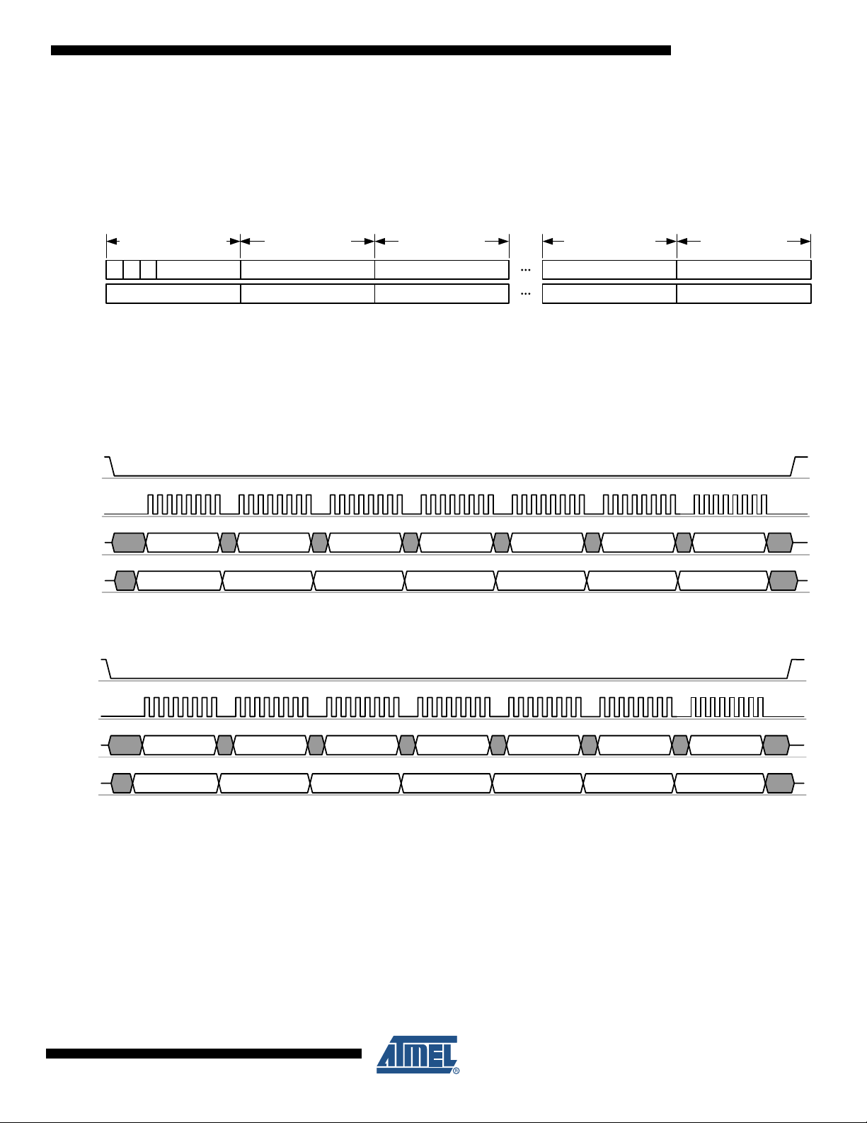
Figure 7-2 on page 39 shows an example for a transmit/receive transaction between two
devices and the related interrupt events in Basic Operating Mode. Device 1 transmits a frame
containing a MAC header (in this example of length 7), payload and valid FCS. The frame is
received by Device 2 which generates the interrupts during the processing of the incoming
frame. The received frame is stored in the Frame Buffer.
The first interrupt IRQ_2 (RX_START) signals the reception of a valid PHR.
If the received frame passes the address filter, refer to Section 7.2.3.5 “Frame Filtering” on page
61, an address match interrupt IRQ_5 (AMI) is issued after the reception of the MAC
header (MHR).
In Basic Operating Mode the third interrupt IRQ_3 (TRX_END) is issued at the end of the
received frame. In Extended Operating Mode, refer to Section 7.2 “Extended Operating Mode”
on page 47; the interrupt is only issued if the received frame passes the address filter and the
FCS is valid. Further exceptions are explained in Section 7.2 “Extended Operating Mode” on
page 47.
Processing delay
istics” on page 157.
f
is a typical value, refer to Section 12.4 “Digital Interface Timing Character-
IRQ
38
AT86RF231
8111A–AVR–05/08
Page 39

Figure 7-2. Timing of RX_START, AMI and TRX_END Interrupts in Basic Operating Mode
128 160 1920 192+(9+m)*32-16 Time [µs]
AT86RF231
TRX_STATE
SLP_TR
IRQ
Typ. Processing Delay
Frame Content
TRX_STATE
IRQ
Interrupt latency
PLL_ON BUSY_TX PLL_ON
16 µs
Preamble
RX_ON RX_ON
7.1.4 Basic Operating Mode Timing
The following paragraphs depict state transitions and their timing properties. Timing figures are
explained in Table 7-1 on page 42 and Section 12.4 “Digital Interface Timing Characteristics” on
page 157.
7.1.4.1 Power-on Procedure
The power-on procedure to P_ON state is shown in Figure 7-3 on page 39.
IRQ_3 (TRX_END)
411 mNumber of Octets
SFD PHR
7
MHR
BUSY_RX
IRQ_2 (RX_START)
t
IRQ
MSDU
t
IRQ
2
FCS
TRX_ENDIRQ_5 (AMI)
t
IRQ
TX
Frame
RX
(Device1)
on Air
(Device 2)
Figure 7-3. Power-on Procedure to P_ON State
0
Event
State
Block
VDD on
P_ON
XOSC, DVREG
Time
When the external supply voltage (V
100
400 Time [µs]
CLKM on
t
TR1
) is firstly supplied to the AT86RF231, the radio trans-
DD
ceiver enables the crystal oscillator (XOSC) and the internal 1.8V voltage regulator for the digital
domain (DVREG). After t
= 380 µs (typ.), the master clock signal is available at pin 17
TR1
(CLKM) at default rate of 1 MHz. If CLKM is available the SPI is already enabled and can be
used to control the transceiver. As long as no state change towards state TRX_OFF is performed the radio transceiver remains in P_ON state.
8111A–AVR–05/08
39
Page 40

7.1.4.2 Wake-up Procedure
The wake-up procedure from SLEEP state is shown in Figure 7-4 on page 40.
Figure 7-4. Wake-up Procedure from SLEEP State
Event
State
SLEEP
Block
Time
The radio transceivers SLEEP state is left by releasing pin SLP_TR to logic low. This restarts the
XOSC and DVREG. After t
internal clock signal is available and provided to pin 17 (CLKM), if CLKM was enabled.
This procedure is similar to the Power-On Procedure. However the radio transceiver continues
the state change automatically to the TRX_OFF state. During this the filter-tuning network (FTN)
calibration is performed. Entering TRX_OFF state is signaled by IRQ_4 (AWAKE_END), if this
interrupt was enabled by the appropriate mask register bit.
7.1.4.3 PLL_ON and RX_ON States
The transition from TRX_OFF to PLL_ON and RX_ON mode is shown in Figure 7-5 on page 40.
Figure 7-5. Transmission from TRX_OFF to PLL_ON and RX_ON State
0
XOSC, DVREG XOSC, DVREGFTN
100
CLKM on
t
TR2
= 240 µs (typ.) the radio transceiver enters TRX_OFF state. The
TR2
200
IRQ_4 (AWAKE_END)SLP_TR = L
TRX_OFF
400
Time [µs]
Event
State
TRX_OFF
Block
Command
Time
0
AVREG
PLL_ON
PLL
t
TR4
100 Time [µs]
IRQ_0 (PLL_LOCK)
PLL_ON
RX_ON
RX
R_ON
t
TR8
Note: If TRX_CMD = RX_ON in TRX_OFF state RX_ON state is entered immediately, even if the PLL
has not settled.
In TRX_OFF state, entering the commands PLL_ON or RX_ON initiates a ramp-up sequence of
the internal 1.8V voltage regulator for the analog domain (AVREG). RX_ON state can be
entered any time from PLL_ON state regardless whether the PLL has already locked, which is
indicated by IRQ_0 (PLL_LOCK).
40
AT86RF231
8111A–AVR–05/08
Page 41

7.1.4.4 BUSY_TX and RX_ON States
The transition from PLL_ON to BUSY_TX state and subsequent to RX_ON state is shown in
Figure 7-6 on page 41.
Figure 7-6. PLL_ON to BUSY_TX to RX_ON Timing
AT86RF231
Time [µs]0x16 x + 32
Starting from PLL_ON state it is further assumed that the PLL is already locked. A transmission
is initiated either by a rising edge of pin 11 (SLP_TR) or by command TX_START. The PLL settles to the transmit frequency and the PA is enabled.
t
TR10
the internally generated SHR is transmitted. After that the PSDU data are transmitted from the
Frame Buffer.
After completing the frame transmission, indicated by IRQ_3 (TRX_END), the PLL settles back
to the receive frequency within t
If during TX_BUSY the radio transmitter is programmed to change to a receive state it automatically proceeds the state change to RX_ON state after finishing the transmission.
7.1.4.5 Reset Procedure
The radio transceiver reset procedure is shown in Figure 7-7 on page 41.
Pin
State
Block
Command
Time
PLL_ON RX_ONBUSY_TX
SLP_TR
PA PLLPA, TX RXPLL
or command TX_START
t
TR10
RX_ON
t
TR11
= 16 µs after initiating the transmission the AT86RF231 changes into BUSY_TX state and
= 32 µs in state PLL_ON.
TR11
8111A–AVR–05/08
Figure 7-7. Reset Procedure
0
Event
State
Block
various
XOSC, DVREG XOSC, DVREG
Pin /RST
Time
Note: Timing figure t
Timing Characteristics” on page 157.
>t10 t
refers to Table 7-1 on page 42, t10, t11 refers to Section 12.4 “Digital Interface
TR13
x
x + 10
FTN
>t11
TR13
x + 40
[IRQ_4 (AWAKE_END)]
TRX_OFF
Time [µs]
41
Page 42

/RST = L sets all registers to their default values. Exceptions are register bits CLKM_CTRL (register 0x03, TRX_CTRL_0), refer to Section 9.6.4 “Master Clock Signal Output (CLKM)” on page
117.
After releasing the reset pin (/RST = H) the wake-up sequence including an FTN calibration
cycle is performed, refer to Section 9.8 “Automatic Filter Tuning (FTN)” on page 125. After that
the TRX_OFF state is entered.
Figure 7-7 on page 41 illustrates the reset procedure once the P_ON state was left and the radio
transceiver was not in SLEEP state.
The reset procedure is identical for all originating radio transceiver states except of state P_ON
and SLEEP state. Instead, here the procedure described in Section 7.1.2.1 “P_ON - Power-On
after VDD” on page 34 must be followed to enter the TRX_OFF state.
If the radio transceiver was in SLEEP state, the XOSC and DVREG are enabled before entering
TRX_OFF state.
If register TRX_STATUS indicates STATE_TRANSITION_IN_PROGRESS during system initialization until the AT86RF231 reaches TRX_OFF, do not try to initiate a further state change while
the radio transceiver is in this state.
Notes
• The reset impulse should have a minimum length t
“Digital Interface Timing Characteristics” on page 157, see parameter 12.4.13.
• An access to the device should not occur earlier than t
/RST; refer to Section 12.4 “Digital Interface Timing Characteristics” on page 157, parameter
12.4.14.
• A reset overrides an SPI command request that might be queued.
7.1.4.6 State Transition Timing Summary
The transition numbers correspond to Figure 7-1 on page 33 and do not include SPI access time
if not otherwise stated. See measurement setup in Figure 5-1 on page 12.
Table 7-1. State Transition Timing
No Symbol Transition Time [µs], (type) Comments
1t
2t
3t
4
5t
6t
7t
8t
9t
t
TR1
TR2
TR3
TR4
TR5
TR6
TR7
TR8
TR9
P_ON
SLEEP TRX_OFF 240
TRX_OFF SLEEP 35*1/f
TRX_OFF PLL_ON 110 Depends on external capacitor at AVDD (1 µF nom)
PLL_ON TRX_OFF 1
TRX_OFF RX_ON 110 Depends on external capacitor at AVDD (1 µF nom)
RX_ON TRX_OFF 1
PLL_ON RX_ON 1
RX_ON PLL_ON 1 Transition time is also valid for TX_ARET_ON, RX_AACK_ON
⇒
⇒
⇒
⇒
⇒
⇒
⇒
⇒
⇒
until CLKM
available
380
CLKM
Depends on external capacitor at DVDD (1 µF nom) and crystal
oscillator setup (CL = 10 pF)
Depends on external capacitor at DVDD (1 µF nom) and crystal
oscillator setup (CL = 10 pF)
TRX_OFF state indicated by IRQ_4 (AWAKE_END)
For f
CLKM
10
> 250 kHz
= 625 ns as specified in Section 12.4
≥ 625 ns after releasing the pin
11
42
AT86RF231
8111A–AVR–05/08
Page 43

Table 7-1. State Transition Timing (Continued)
No Symbol Transition Time [µs], (type) Comments
When asserting pin 11 (SLP_TR) or TRX_CMD = TX_START
10 t
TR10
PLL_ON BUSY_TX 16
⇒
first symbol transmission is delayed by 16 µs delay (PLL
settling and PA ramp up)
11 t
TR11
BUSY_TX PLL_ON 32 PLL settling time from TX_BUSY to PLL_ON state
⇒
Using TRX_CMD = FORCE_TRX_OFF (see register 0x02,
12 t
TR12
All modes TRX_OFF 1
⇒
TRX_STATE),
Not valid for SLEEP state
13 t
14 t
TR13
TR14
RESET TRX_OFF 37 Valid for P_ON or SLEEP state
Var ious
States
⇒
⇒
PLL_ON 1
Using TRX_CMD = FORCE_PLL_ON (see register 0x02,
TRX_STATE),
Not valid for SLEEP, P_ON, RESET, TRX_OFF and *_NO_CLK
The state transition timing is calculated based on the timing of the individual blocks shown in
Figure 7-3 on page 39 to Figure 7-7 on page 41. The worst case values include maximum oper-
ating temperature, minimum supply voltage, and device parameter variations.
Table 7-2. Analog Block Initialization and Settling Time
AT86RF231
No Symbol Block Time [µs], (type) Time [µs], (max) Comment
15 t
16 t
17 t
18 t
19 t
20 t
21 t
22 t
23 t
24 t
25 t
26 t
27 t
28 t
29 t
TR15
TR16
TR17
TR18
TR19
TR20
TR21
TR22
TR23
TR24
TR25
TR26
TR27
TR28
TR29
XOSC 215 1000
FTN 25 FTN tuning time fixed
DVR EG 60 1000
AVR EG 60 1000
PLL, initial 110 155
PLL settling 11 24 Settling time between channels switch
PLL, CF cal 35 PLL center frequency calibration, refer to Section 9.7.4
PLL, DCU cal 6 PLL DCU calibration, refer to Section 9.7.4
PLL, RX TX 16 Maximum PLL settling time RX TX
PLL, TX RX 32 Maximum PLL settling time TX RX
⇒ ⇒
⇒ ⇒
RSSI, update 2 RSSI update period in receive states, refer to Section 8.3.2
ED 140 ED measurement period, refer to Section 8.4.2
SHR, sync 96 Typical SHR synchronisation period, refer to Section 8.4.2
CCA 140 CCA measurement period, refer to Section 8.5.2
Random value 1 Random value update period, refer to Section 11.2.1
Leaving SLEEP state, depends on crystal Q factor and
load capacitor
Depends on external bypass capacitor at DVDD
(CB3 = 1 µF nom., 10 µF worst case), depends on V
Depends on external bypass capacitor at AVDD
(CB1 = 1 µF nom, 10 µF worst case), depends on V
PLL settling time TRX_OFF PLL_ON, including 60 µs
AVREG settling time
DD
DD
⇒
8111A–AVR–05/08
43
Page 44

7.1.5 Register Description Register 0x01 (TRX_STATUS):
A read access to TRX_STATUS register signals the current radio transceiver state. A state
change is initiated by writing a state transition command to register bits TRX_CMD (register
0x02, TRX_STATE). Alternatively a state transition can be initiated by the rising edge of pin 11
(SLP_TR) in the appropriate state.
This register is used for Basic and Extended Operating Mode, refer to Section 7.2 “Extended
Operating Mode” on page 47.
Bit 7 6 5 4 3 2 1 0
+0x01 CCA_DONE CCA_STATUS Reserved TRX_STATUS TRX_STATUS
Read/Write R R R R R R R R
Reset Value 0 0 0 0 0 0 0 0
• Bit 7 - CCA_DONE
Refer to Section 8.5 “Clear Channel Assessment (CCA)” on page 94.
• Bit 6 - CCA_STATUS
Refer to Section 8.5 “Clear Channel Assessment (CCA)” on page 94.
• Bit 5 - Reserved
• Bit [4:0] - TRX_STATUS
The register bits TRX_STATUS signals the current radio transceiver status. If the requested
state transition is not completed yet, the TRX_STATUS returns
STATE_TRANSITION_IN_PROGRESS. Do not try to initiate a further state change while the
radio transceiver is in STATE_TRANSITION_IN_PROGRESS. State transition timings are
defined in Table 7-1 on page 42.
44
AT86RF231
8111A–AVR–05/08
Page 45

Table 7-3. Radio Transceiver Status, Register Bits TRX_STATUS
Register Bits Value State Description
AT86RF231
TRX_STATUS 0x00
P_ON
0x01 BUSY_RX
0x02 BUSY_TX
0x06 RX_ON
0x08 TRX_OFF (CLK Mode)
0x09 PLL_ON (TX_ON)
0x0F
0x11
0x12
0x16
0x19
(3)
(1)
(1)
(1)
(1)
SLEEP
BUSY_RX_AACK
BUSY_TX_ARET
RX_AACK_ON
TX_ARET_ON
0x1C RX_ON_NOCLK
(1)
0x1D
0x1E
0x1F
(1)
(2)
RX_AACK_ON_NOCLK
BUSY_RX_AACK_NOCLK
STATE_TRANSITION_IN_PROGRESS
All other values are reserved
Notes: 1. Extended Operating Mode only, refers to Section 7.2 “Extended Operating Mode” on page 47.
2. Do not try to initiate a further state change while the radio transceiver is in
STATE_TRANSITION_IN_PROGRESS state.
3. In SLEEP state register not accessible.
8111A–AVR–05/08
45
Page 46

Register 0x02 (TRX_STATE):
The radio transceiver states are controlled via register bits TRX_CMD, which receives the state
transition commands.
This register is used for Basic and Extended Operating Mode, refer to Section 7.2 “Extended
Operating Mode” on page 47.
Bit 765 43210
+0x02 TRAC_STATUS TRX_CMD TRX_STATE
Read/Write R R R R/W R/W R/W R/W R/W
Reset Value 0 0 0 0 0 0 0 0
• Bit [7:5] - TRAC_STATUS
Refer to Section 7.2.7 “Register Description - Control Registers” on page 68.
• Bit [4:0] - TRX_CMD
A write access to register bits TRX_CMD initiate a radio transceiver state transition towards the
new state as defined by the write access:
Table 7-4. State Control Command, Register Bits TRX_CMD
Register Bit Value State Description
TRX_CMD 0x00
NOP
0x02 TX_START
0x03 FORCE_TRX_OFF
0x04
(1)
FORCE_PLL_ON
0x06 RX_ON
0x08 TRX_OFF (CLK Mode)
0x09 PLL_ON (TX_ON)
0x16
0x19
(2)
(2)
RX_AACK_ON
TX_ARET_ON
All other values are reserved and mapped to NOP
Notes: 1. FORCE_PLL_ON is not valid for states SLEEP, P_ON, RESET, TRX_OFF, and all *_NOCLK
states, as well as STATE_TRANSITION_IN_PROGRESS towards these states.
2. Extended Operating Mode only, refers to Section 7.2.7 “Register Description - Control Regis-
ters” on page 68.
46
AT86RF231
8111A–AVR–05/08
Page 47

7.2 Extended Operating Mode
The Extended Operating Mode is a hardware MAC accelerator and goes beyond the basic radio
transceiver functionality provided by the Basic Operating Mode. It handles time critical MAC
tasks, requested by the IEEE 802.15.4 standard, by hardware, such as automatic acknowledgement, automatic CSMA-CA and retransmission. This results in a more efficient IEEE 802.15.4
software MAC implementation including reduced code size and may allow the use of a smaller
microcontroller or to operate at low clock rates.
The Extended Operating Mode is designed to support IEEE 802.15.4-2006 compliant frames;
the mode is backward compatible to IEEE 802.15.4-2003 and supports non IEEE 802.15.4 compliant frames. This mode comprises the following procedures:
Automatic acknowledgement (RX_AACK) divides into the tasks:
• Frame reception and automatic FCS check
• Configurable addressing fields check
• Interrupt indicating address match
• Interrupt indicating frame reception, if it passes address filtering and FCS check
• Automatic ACK frame transmission (if the received frame passed the address filter and FCS
check and if an ACK is required by the frame type and ACK request)
• Support of slotted acknowledgment using SLP_TR pin
AT86RF231
Automatic CSMA-CA and Retransmission (TX_ARET) divides into the tasks:
• CSMA-CA including automatic CCA retry and random back-off
• Frame transmission and automatic FCS field generation
• Reception of ACK frame (if an ACK was requested)
• Automatic frame retry if ACK was expected but not received
• Interrupt signaling with transaction status
Automatic FCS check and generation, refer to Section 8.2 “Frame Check Sequence (FCS)” on
page 85, is used by the RX_AACK and TX_ARET modes. In RX_AACK mode, an automatic
FCS check is always performed for incoming frames.
In TX_ARET mode, an ACK, received within the time required by IEEE 802.15.4, is accepted if
the FCS is valid, and if the sequence number of the ACK matches the sequence number of the
previously transmitted frame. Dependent on the value of the frame pending subfield in the
received acknowledgement frame the transaction status is set, see Table 7-16 on page 70.
An AT86RF231 state diagram including the Extended Operating Mode states is shown in Figure
7-8 on page 48. Yellow marked states represent the Basic Operating Mode; blue marked states
represent the Extended Operating Mode.
8111A–AVR–05/08
47
Page 48

Figure 7-8. Extended Operating Mode State Diagram
P_ON
(Power-on after VDD)
XOSC=ON
Pull=ON
T
R
X
_
O
F
BUSY_RX
(Receive State)
SHR
Detected
RX_ON_NOCLK
(Rx Listen State)
CLKM=OFF
FORCE_TRX_OFF
(all modes except SLEEP)
6
SHR
Detected
RX_ON
H
=
R
R=L
T
P_
SL
(Rx Listen State)
_
K
C
AA
_
RX
Frame
End
T
_
P
L
S
SHR
Detected
F
1
N
O
TRX_OFF
(Clock State)
F
O
_
X
R
T
8
12 13
_
X
R
From / To
TRX_OFF
N
O
F
F
O
_
RX
T
XOSC=ON
Pull=OFF
F
RX_ON
PLL_ON
O
L_
L
P
2
N
_
X
R
BUSY_RX_AACK BUSY_TX_ARET
Transaction
Finished
R
T
_
P
L
S
57
T
R
X
_
O
F
F
9
N
O
_
K
C
A
A
SLEEP
(Sleep State)
XOSC=OFF
Pull=OFF
S
=L
_
P
L
P
L
3
=H
R
T
/RST = H
(all modes except P_ON)
L
_
O
N
4
PLL_ON
(PLL State)
PLL_ON
TX_ARET_ON
TX_ARET_ONRX_AACK_ON
SLP_TR=H
TX_START
14
FORCE_PLL_ON
From / To
TRX_OFF
N
O
_
T
E
O
R
_
A
X
_
R
X
T
T
SLP_TR=H
TX_START
or
11
10
Frame
End
see notes
F
F
or
Frame
End
(from all states)
/RST = L
RESET
BUSY_TX
(Transmit State)
48
Frame
Accepted
SHR
BUSY_RX_
Detected
AACK_NOCLK
CLKM=OFF CLKM=OFF
Frame
Rejected
RX_AACK_
ON_NOCLK
AT86RF231
SLP_TR=L
SLP_TR=H
Legend:
Blue: SPI Write to Register TRX_STATE (0x02)
Red: Control signals via IC Pin
Green: Event
Basic Operating Mode States
Extended Operating Mode States
8111A–AVR–05/08
Page 49

7.2.1 State Control
AT86RF231
The Extended Operating Mode states RX_AACK and TX_ARET are controlled via register bits
TRX_CMD (register 0x02, TRX_STATE), which receives the state transition commands. The
states are entered from TRX_OFF or PLL_ON state as illustrated by Figure 7-8 on page 48. The
completion of each state change command shall always be confirmed by reading the register
0x01 (TRX_STATUS).
RX_AACK - Receive with Automatic ACK
A state transition to RX_AACK_ON from PLL_ON or TRX_OFF is initiated by writing the command RX_AACK_ON to the register bits TRX_CMD. The state change can be confirmed by
reading register 0x01 (TRX_STATUS), those changes to RX_AACK_ON or BUSY_RX_AACK
on success. The latter one is returned if a frame is currently about being received.
The RX_AACK state is left by writing command TRX_OFF or PLL_ON to the register bits
TRX_CMD. If the AT86RF231 is within a frame receive or acknowledgment procedure
(BUSY_RX_AACK) the state change is executed after finish. Alternatively, the commands
FORCE_TRX_OFF or FORCE_PLL_ON can be used to cancel the RX_AACK transaction and
change into radio transceiver state TRX_OFF or PLL_ON, respectively.
TX_ARET - Transmit with Automatic Retry and CSMA-CA Retry
Similarly, a state transition to TX_ARET_ON from PLL_ON or TRX_OFF is initiated by writing
command TX_ARET_ON to register bits TRX_CMD. The radio transceiver is in the
TX_ARET_ON state after TRX_STATUS (register 0x01) changes to TX_ARET_ON. The
TX_ARET transaction is started with a rising edge of pin 11 (SLP_TR) or writing the command
TX_START to register bits TRX_CMD.
The TX_ARET state is left by writing the command TRX_OFF or PLL_ON to the register bits
TRX_CMD. If the AT86RF231 is within a CSMA-CA, a frame-transmit or an acknowledgment
procedure (BUSY_TX_ARET) the state change is executed after finish. Alternatively the command FORCE_TRX_OFF or FORCE_PLL_ON can be used to instantly terminate the TX_ARET
transaction and change into radio transceiver state TRX_OFF or PLL_ON, respectively.
Note
• A state change request from TRX_OFF to RX_AACK_ON or TX_ARET_ON internally
passes the state PLL_ON to initiate the radio transceiver. Thus the readiness to receive or
transmit data is delayed accordingly. It is recommended to use interrupt IRQ_0 (PLL_LOCK)
as an indicator.
8111A–AVR–05/08
49
Page 50

7.2.2 Configuration
The use of the Extended Operating Mode is based on Basic Operating Mode functionality. Only
features beyond the basic radio transceiver functionality are described in the following sections.
For details on the Basic Operating Mode refer to Section 7.1 “Basic Operating Mode” on page
33.
When using the RX_AACK or TX_ARET modes, the following registers needs to be configured.
RX_AACK configuration steps:
• Short address, PAN-ID and IEEE address
• Configure RX_AACK properties
– Handling of Frame Version Subfield
– Handling of Pending Data Indicator
– Characterize as PAN coordinator
– Handling of Slotted Acknowledgement
• Additional Frame Filtering Properties
– Promiscuous Mode
– Enable or disable automatic ACK generation
– Handling of reserved frame types
The addresses for the address match algorithm are to be stored in the appropriate address registers. Additional control of the RX_AACK mode is done with register 0x17 (XAH_CTRL_1) and
register 0x2E (CSMA_SEED_1).
As long as a short address has not been set, only broadcast frames and frames matching the
IEEE address can be received.
Configuration examples for different device operating modes and handling of various frame
types can be found in Section 7.2.3.1 “Description of RX_AACK Configuration Bits” on page 54.
registers 0x20 - 0x2B
registers 0x2C, 0x2E
registers 0x17, 0x2E
50
TX_ARET configuration steps:
• Leave register bit TX_AUTO_CRC_ON = 1 register 0x04, TRX_CTRL_1
• Configure CSMA-CA
– MAX_FRAME_RETRIES register 0x2C, XAH_CTRL_0
– MAX_CSMA_RETRIES register 0x2C, XAH_CTRL_0
– CSMA_SEED registers 0x2D, 0x2E
– MAX_BE, MIN_BE register 0x2F, CSMA_BE
• Configure CCA (see Section 8.5)
MAX_FRAME_RETRIES (register 0x2C) defines the maximum number of frame
retransmissions.
The register bits MAX_CSMA_RETRIES (register 0x2C) configure the number of CSMA-CA
retries after a busy channel is detected.
AT86RF231
8111A–AVR–05/08
Page 51

The CSMA_SEED_0 and CSMA_SEED_1 register bits (registers 0x2D, 0x2E) define a random
seed for the back-off-time random-number generator in theAT86RF231.
The MAX_BE and MIN_BE register bits (register 0x2F) sets the maximum and minimum CSMA
back-off exponent (according to [1]).
7.2.3 RX_AACK_ON - Receive with Automatic ACK
The general functionality of the RX_AACK procedure is shown in Figure 7-9 on page 53.
The gray shaded area is the standard flow of an RX_AACK transaction for IEEE 802.15.4 compliant frames, refer Section 7.2.3.2 “Configuration of IEEE Scenarios” on page 55. All other
procedures are exceptions for specific operating modes or frame formats, refer to Section
7.2.3.3 “Configuration of non IEEE 802.15.4 Compliant Scenarios” on page 58.
The frame filtering operations is described in detail in Section 7.2.3.5 “Frame Filtering” on page
61.
In RX_AACK_ON state, the radio transceiver listens for incoming frames. After detecting a valid
PHR, the radio transceiver parses the frame content of the MAC header (MHR), refer to Section
8.1.2 “MAC Protocol Layer Data Unit (MPDU)” on page 80.
AT86RF231
Generally, at nodes, configured as a normal device or PAN coordinator, a frame is not indicated
if the frame filter does not match and the FCS is invalid. Otherwise, the interrupt IRQ_3
(TRX_END) is issued after the completion of the frame reception. The microcontroller can then
read the frame. An exception applies if promiscuous mode is enabled; see Section 7.2.3.2 “Con-
figuration of IEEE Scenarios” on page 55, in that case an IRQ_3 (TRX_END) interrupt is issued,
even if the FCS fails.
If the content of the MAC addressing fields of the received frame (refer to IEEE 802.15.4 section
7.2.1) matches one of the configured addresses, dependent on the addressing mode, an
address match interrupt IRQ_5 (AMI) is issued, refer to Section 7.2.3.5 “Frame Filtering” on
page 61. The expected address values are to be stored in registers 0x20 - 0x2B (Short address,
PAN-ID and IEEE address). Frame filtering as described in Section 7.2.3.5 “Frame Filtering” on
page 61 is also valid for Basic Operating Mode.
During reception the AT86RF231 parses bit [5] (ACK Request) of the frame control field of the
received data or MAC command frame to check if an ACK reply is expected. In that case and if
the frame passes the third level of filtering, see IEEE 802.15.4-2006, section 7.5.6.2, the radio
transceiver automatically generates and transmits an ACK frame.
The content of the frame pending subfield of the ACK response is set by register bit
AACK_SET_PD (register 0x2E, CSMA_SEED_1) when the ACK frame is sent in response to a
data request MAC command frame, otherwise this subfield is set to 0. The sequence number is
copied from the received frame.
Optionally, the start of the transmission of the acknowledgement frame can be influenced by
register bit AACK_ACK_TIME. Default value (according to standard IEEE 802.15.4) is 12 symbol times after the reception of the last symbol of a data or MAC command frame.
8111A–AVR–05/08
If the register bit AACK_DIS_ACK (register 0x2E, CSMA_SEED_1) is set, no acknowledgement
frame is sent even if an acknowledgment frame was requested. This is useful for operating the
MAC hardware accelerator in promiscuous mode, see Section 7.2.3.2 “Configuration of IEEE
Scenarios” on page 55.
51
Page 52

The status of the RX_AACK operation is indicated by register bits TRAC_STATUS (register
0x02, TRAC_STATUS), see Section 7.2.7 “Register Description - Control Registers” on page
68.
During the operations described above the AT86RF231 remains in BUSY_RX_AACK state.
52
AT86RF231
8111A–AVR–05/08
Page 53

Figure 7-9. Flow Diagram of RX_AACK
AT86RF231
TRX_STATE = RX_AACK_ON
Note 1: Address match, Promiscuous Mode and
Reserved Frames:
- A radio transceiver in Promiscuous
Mode, or configured to receive Reserved
Frames handles received frames passing
the third level of filtering
- For details refer to the description of
Promiscuous Mode and Reserved
Frame Types
Note 2: FCS check is omitted for Promiscous Mode
Note 3: Additional conditions:
- ACK requested &
- ACK_DIS_ACK==0 &
- frame_version<=AACK_FVN_MODE
N
AACK_ACK_TIME
== 0
Y
Wait 2 symbol
periods
Wait 6 symbol
periods
SHR detected
TRX_STATE = BUSY_RX_AACK
Generate IRQ_2 (RX_START)
Scanning MHR
Frame Filtering
Y
Generate IRQ_5 (AMI)
Frame reception
N
FCS valid
(see Note 2)
Generate IRQ_3 (TRX_END)
N
ACK requested
(see Note 3)
N
Slotted Operatio n
== 0
AACK_ACK_TIME
== 0
Wait 12 symbol
periods
N
Y
N
(see Note 1)
Y
Y
Y
Y
N
Wait 2 symbol
periods
Promiscuous M ode
Frame reception
AACK_PROM_MODE
== 1
Y
Generate IRQ_3
(TRX_END)
Reserved Frames
N
N
FCF[2:0]
> 3
Y
N
AACK_UPLD_RES_FT
== 1
Y
N
FCS valid
Y
Generate IRQ_3
(TRX_END)
8111A–AVR–05/08
pin 11 (SLP_TR)
rising edge
Y
N
Transmit ACK
TRX_STATE = RX_AACK_ON
53
Page 54

7.2.3.1 Description of RX_AACK Configuration Bits
Overview
Table 7-5 on page 54 summarizes all register bits which affect the behavior of an RX_AACK
transaction. For address filtering it is further required to setup address registers to match to the
expected address.
Configuration and address bits are to be set in TRX_OFF or PLL_ON state prior to switching to
RX_AACK mode.
A graphical representation of various operating modes is illustrated in Figure 7-9 on page 53.
Table 7-5. Overview of RX_AACK Configuration Bits
Register Register Register Name Description
Address Bits
0x20,0x21
0x22,0x23
0x24
...........
0x2B
0x0C 7 RX_SAFE_MODE Protect buffer after frame receive
0x17 1 AACK_PROM_MODE Support promiscuous mode
0x17 2 AACK_ACK_TIME Change auto acknowledge start time
0x17 4 AACK_UPLD_RES_FT Enable reserved frame type reception, needed
0x17 5 AACK_FLTR_RES_FT Filter reserved frame types like data frame
0x2C 0 SLOTTED_OPERATION If set, acknowledgment transmission has to be
0x2E 3 AACK_I_AM_COORD If set, the device is a PAN coordinator
0x2E 4 AACK_DIS_ACK Disable generation of acknowledgment
0x2E 5 AACK_SET_PD Set frame pending subfield in Frame Control
0x2E 7:6 AACK_FVN_MODE Controls the ACK behavior, depending on FCF
SHORT_ADDR_0/1
PAN_ADDR_0/1
IEEE_ADDR_0
........
IEEE_ADDR_7
Set node addresses
to receive non-standard compliant frames
type, needed for filtering of non-standard
compliant frames
triggered by pin 11 (SLP_TR)
Field (FCF), refer to Section 8.1.2.2
frame version number
54
The usage of the RX_AACK configuration bits for various operating modes of a node is
explained in the following sections. Configuration bits not mentioned in the following two sections should be set to their reset values according to Table 14-1 on page 167.
All registers mentioned in Table 7-5 on page 54 are described in Section 7.2.6 “Register Sum-
mary” on page 68.
Note, that the general behavior of the "AT86RF231 Extended Feature Set", Section 11.
“AT86RF231 Extended Feature Set” on page 128, settings:
AT86RF231
8111A–AVR–05/08
Page 55

• OQPSK_DATA_RATE (PSDU data rate)
• SFD_VALUE (alternative SFD value)
• ANT_DIV (Antenna Diversity)
• RX_PDT_LEVEL (blocking frame reception of lower power signals)
are completely independent from RX_AACK mode. Each of these operating modes can be combined with the RX_AACK mode.
7.2.3.2 Configuration of IEEE Scenarios
Normal Device
Table 7-6 on page 55 shows a typical RX_AACK configuration of an IEEE 802.15.4 device oper-
ating as a normal device, rather than a PAN coordinator or router.
Table 7-6. Configuration of IEEE 802.15.4 Devices
Register Register Register Name Description
Address Bits
AT86RF231
0x20,0x21
0x22,0x23
0x24,
...........
0x2B
0x0C 7 RX_SAFE_MODE 0
0x2C 0 SLOTTED_OPERATION 0: if transceiver works in unslotted mode
0x2E 7:6 AACK_FVN_MODE Controls the ACK behavior, depending on FCF
SHORT_ADDR_0/1
PAN_ADDR_0/1
IEEE_ADDR_0
........
IEEE_ADDR_7
Set node addresses
: disable frame protection
1: enable frame protection
1: if transceiver works in slotted mode
frame version number
0x00: acknowledges only frames with version
number 0, i.e. according to IEEE 802.15.4-2003
frames
0x01
: acknowledges only frames with version
number 0 or 1, i.e. frames according to IEEE
802.15.4-2006
0x10: acknowledges only frames with version
number 0 or 1 or 2
0x11: acknowledges all frames, independent of
the FCF frame version number
Notes
8111A–AVR–05/08
• If no short address has been configured before the device has been assigned one by the
PAN-coordinator, only frames directed to either the broadcast address or the IEEE address
are received.
• In IEEE 802.15.4-2003 standard the frame version subfield did not yet exist but was marked
as reserved. According to this standard, reserved fields have to be set to zero. On the other
hand, IEEE 802.15.4-2003 standard requires ignoring reserved bits upon reception. Thus,
there is a contradiction in the standard which can be interpreted in two ways:
55
Page 56

1.
If a network should only allow access to nodes which use the IEEE 802.15.4-2003,
then AACK_FVN_MODE should be set to 0.
2.
If a device should acknowledge all frames independent of its frame version,
AACK_FVN_MODE should be set to 3. However, this can result in conflicts with
co-existing IEEE 802.15.4-2006 standard compliant networks.
The same holds for PAN coordinators, see Table 7-7 on page 56.
PAN-Coordinator
Table 7-7. Configuration of a PAN Coordinator
Register Register Register Name Description
Address Bits
0x20,0x21
0x22,0x23
0x24,
...........
0x2B
0x0C 7 RX_SAFE_MODE 0
SHORT_ADDR_0/1
PAN_ADDR_0/1
IEEE_ADDR_0
........
IEEE_ADDR_7
Set node addresses
: disable frame protection
1: enable frame protection
0x2C 0 SLOTTED_OPERATION 0
0x2E 3 AACK_I_AM_COORD 1: device is PAN coordinator
0x2E 5 AACK_SET_PD 0
0x2E 7:6 AACK_FVN_MODE Controls the ACK behavior, depending on FCF
: if transceiver works in unslotted mode
1: if transceiver works in slotted mode
: frame pending subfield is not set in FC
1: frame pending subfield is set in FCF
frame version number
0x00: acknowledges only frames with version
number 0, i.e. according to IEEE 802.15.4-2003
frames
0x01
: acknowledges only frames with version
number 0 or 1, i.e. frames according to IEEE
802.15.4-2006
0x10: acknowledges only frames with version
number 0 or 1 or 2
0x11: acknowledges all frames, independent of
the FCF frame version number
Promiscuous Mode
The promiscuous mode is described in IEEE 802.15.4-2006, section 7.5.6.2. This mode is further illustrated in Figure 7-9 on page 53. According to IEEE 802.15.4-2006 when in promiscuous
mode, the MAC sub layer shall pass received frames with correct FCS to the next higher layer
and shall not be processed further. That implies that frames should never be acknowledged.
56
AT86RF231
8111A–AVR–05/08
Page 57

AT86RF231
Only second level filter rules as defined by IEEE 802.15.4-2006, section 7.5.6.2, are applied to
the received frame.
Table 7-8 on page 57 shows the typical configuration of a device operating promiscuous mode.
Table 7-8. Configuration of Promiscuous Mode
Register Register Register Name Description
Address Bits
0x20,0x21
0x22,0x23
0x24,
...
0x2B
0x17 1 AACK_PROM_MODE 1: Enable promiscuous Mode
0x2E 4 AACK_DIS_ACK 1: Disable generation of acknowledgment
0x2E 7:6 AACK_FVN_MODE Controls the ACK behavior, depending on FCF
SHORT_ADDR_0/1
PAN_ADDR_0/1
IEEE_ADDR_0
...
IEEE_ADDR_7
Address shall be set: 0x00
frame version number
0x00: acknowledges only frames with version
number 0, i.e. according to IEEE 802.15.4-2003
frames
: acknowledges only frames with version
0x01
number 0 or 1, i.e. frames according to
IEEE 802.15.4-2006
0x10: acknowledges only frames with version
number 0 or 1 or 2
0x11: acknowledges all frames, independent of
the FCF frame version number
If the radio transceiver is in promiscuous mode, second level of filtering according to
IEEE 802.15.4-2006, section 7.5.6.2, is applied to a received frame. However, an IRQ_3
(TRX_END) is issued even if the FCS is invalid. Thus, it is necessary to read register bit
RX_CRC_VALID (register 0x06, PHY_RSSI) after IRQ_3 (TRX_END) in order to verify the
reception of a frame with a valid FCS.
8111A–AVR–05/08
If a device, operating in promiscuous mode, receives a frame with a valid FCS which further
passed the third level of filtering according to IEEE 802.15.4-2006, section 7.5.6.2, an acknowledgement frame would be transmitted. According to the definition of the promiscuous mode a
received frame shall not be acknowledged, even if it is requested. Thus register bit
AACK_DIS_ACK (register 0x2E, CSMA_SEED_1) has to be set to 1.
In all receive modes an IRQ_5 (AMI) interrupt is issued, when the received frame matches the
node's address according to the filter rules described in Section 7.2.3.5 “Frame Filtering” on
page 61
Alternatively, in Basic Operating Mode RX_ON state, when a valid PHR is detected, an IRQ_2
(RX_START) is generated and the frame is received. The end of the frame reception is signalized with an IRQ_3 (TRX_END). At the same time the register bit RX_CRC_VALID (register
0x06, PHY_RSSI) is updated with the result of the FCS check (see Section 8.2 “Frame Check
Sequence (FCS)” on page 85). According to the promiscuous mode definition the
RX_CRC_VALID bit needs to be checked in order to dismiss corrupted frames.
57
Page 58

7.2.3.3 Configuration of non IEEE 802.15.4 Compliant Scenarios
Sniffer
Table 7-9 on page 58 shows an RX_AACK configuration to setup a sniffer device. Other
RX_AACK configuration bits, refer to Table 7-5 on page 54, should be set to their reset values.
All frames received are indicated by an IRQ_2 (RX_START) and IRQ_3 (TRX_END). After
frame reception register bit RX_CRC_VALID (register 0x06, PHY_RSSI) is updated with the
result of the FCS check (see Section 8.2 “Frame Check Sequence (FCS)” on page 85). The
RX_CRC_VALID bit needs to be checked in order to dismiss corrupted frames.
Table 7-9. Configuration of a Sniffer Device
Register Register Register Name Description
Address Bits
0x17 1 AACK_PROM_MODE 1: Enable promiscuous Mode
0x2E 4 AACK_DIS_ACK 1: Disable generation of acknowledgment
This operating mode is similar to the promiscuous mode.
Reception of Reserved Frames
In RX_AACK mode, frames with reserved frame types, refer to Section 8.1.2.2 “Frame Control
Field (FCF)” on page 80, can also be handled. This might be required when implementing propri-
etary, non-standard compliant, protocols. It is an extension of the address filtering in RX_AACK
mode. Received frames are either handled similar to data frames, or may be allowed to completely bypass the address filter.
Table 7-10 on page 58 shows the required configuration for a node to receive reserved frames,
Figure 7-9 on page 53 shows the corresponding flow chart.
Table 7-10. RX_AACK Configuration to Receive Reserved Frame Types
Register Register Register Name Description
Address Bits
0x20,0x21
0x22,0x23
0x24,
...........
0x2B
0x0C 7 RX_SAFE_MODE 0
0x17 4 AACK_UPLD_RES_FT 1: Enable reserved frame type reception
0x17 5 AACK_FLTR_RES_FT Filter reserved frame types like data frame type,
0x2C 0 SLOTTED_OPERATION 0
SHORT_ADDR_0/1
PAN_ADDR_0/1
IEEE_ADDR_0
........
IEEE_ADDR_7
Set node addresses
: disable frame protection
1: enable frame protection
see note below
0
: disable
1: enable
: if transceiver works in unslotted mode
1: if transceiver works in slotted mode
58
AT86RF231
8111A–AVR–05/08
Page 59

AT86RF231
Table 7-10. RX_AACK Configuration to Receive Reserved Frame Types (Continued)
0x2E 3 AACK_I_AM_COORD 0: device is not PAN coordinator
1: device is PAN coordinator
0x2E 4 AACK_DIS_ACK 0: Enable generation of acknowledgment
1: Disable generation of acknowledgment
0x2E 7:6 AACK_FVN_MODE Controls the ACK behavior, depending on FCF
frame version number
0x00: acknowledges only frames with version
number 0, i.e. according to IEEE 802.15.4-2003
frames
0x01
: acknowledges only frames with version
number 0 or 1, i.e. frames according to IEEE
802.15.4-2006
0x10: acknowledges only frames with version
number 0 or 1 or 2
0x11: acknowledges all frames, independent of
the FCF frame version number
There are two different options for handling reserved frame types.
1.
AACK_UPLD_RES_FT = 1, AACK_FLT_RES_FT = 0:
Any non-corrupted frame with a reserved frame type is indicated by an
IRQ_3 (TRX_END) interrupt. No further address filtering is applied on those frames. An
IRQ_5 (AMI) interrupt is never generated and the acknowledgment subfield is ignored.
2.
AACK_UPLD_RES_FT = 1, AACK_FLT_RES_FT = 1:
If AACK_FLT_RES_FT = 1 any frame with a reserved frame type is filtered by the
address filter similar to a data frame as described in the standard. This implies the
generation of the IRQ_5 (AMI) interrupts upon address match. An IRQ_3 (TRX_END)
interrupt is only generated if the address matched and the frame was not corrupted. An
acknowledgment is only send, when the ACK request subfield was set in the received
frame and an IRQ_3 (TRX_END) interrupt occurred.
Note
• It is not allowed to set AACK_FLTR_RES_FT = 1 and have register bit AACK_FLTR_RES_FT
set to 0.
8111A–AVR–05/08
59
Page 60

Short Acknowledgment Frame (ACK) Start Timing
Register bit AACK_ACK_TIME (register 0x17, XAH_CTRL_1), see Table 7-11 on page 60,
defines the symbol time between frame reception and transmission of an acknowledgment
frame.
Table 7-11. Overview of RX_AACK Configuration Bits
Register Register Register Name Description
Address Bit
0x17 2 AACK_ACK_TIME
Note that this feature can be used in all scenarios, independent of other configurations. However, shorter acknowledgment timing is especially useful when using High Data Rate Modes to
increase battery lifetime and to improve the overall data throughput; refer to Section 11.3 “High
Data Rate Modes” on page 137.
7.2.3.4 RX_AACK_NOCLK - RX_AACK_ON without CLKM
If the AT86RF231 is listening for an incoming frame and the microcontroller is not running an
application, the microcontroller can be powered down to decrease the total system power consumption. This special power-down scenario for systems running in clock synchronous mode
(see Section 6. “Microcontroller Interface” on page 16) is supported by the AT86RF231 using the
state RX_AACK_ON_NOCLK. The radio transceiver functionality in this state is based on that in
state RX_AACK_ON with pin 17 (CLKM) disabled.
: Standard compliant acknowledgement timing
0
of 12 symbol periods. In slotted acknowledgement operation mode, the acknowledgment
frame transmission can be triggered 6 symbol
periods after reception of the frame earliest.
1: Reduced acknowledgment timing of 2 symbol
periods (32 µs).
The RX_AACK_NOCLK state is entered from RX_AACK_ON by a rising edge at pin 11
(SLP_TR). The return to RX_AACK_ON state results either from a successful frame reception or
a falling edge on pin SLP_TR.
The CLKM pin is disabled 35 clock cycles after the rising edge at SLP_TR pin. This allows the
microcontroller to complete its power-down sequence. This is not valid for clock rates 250 kHz
and 62.5 kHz, where the main clock at pin 17 (CLKM) is switched off immediately.
In case of the reception of a valid frame, IRQ_3 (TRX_END) is issued and pin 17 (CLKM) is
turned on. A timing diagram is shown in Figure 6-16 on page 28. A received frame is considered
valid if it passes address filtering and has a correct FCS. If an ACK was requested the radio
transceiver enters BUSY_RX_AACK state and follows the procedure described in Section 7.2.3
“RX_AACK_ON - Receive with Automatic ACK” on page 51.
After the transaction has been completed, the radio transceiver reenters the RX_AACK_ON
state.
The radio transceiver reenters the RX_AACK_ON_NOCLK state only, when the next rising edge
at SLP_TR pin occurs.
60
AT86RF231
8111A–AVR–05/08
Page 61

7.2.3.5 Frame Filtering
Frame Filtering is an evaluation whether or not a received frame is dedicated for this node. To
accept a received frame and to generate an address match interrupt IRQ_5 (AMI) a filtering procedure as described in IEEE 802.15.4-2006, section 7.5.6.2 (Third level of filtering) is applied to
the frame. The AT86RF231 RX_AACK mode accepts only frames that satisfy all of the following
requirements (quote from IEEE 802.15.4-2006, section 7.5.6.2):
AT86RF231
1.
The Frame Type subfield shall not contain a reserved frame type.
2.
The Frame Version subfield shall not contain a reserved value.
3.
If a destination PAN identifier is included in the frame, it shall match macPANId or shall
be the broadcast PAN identifier (0xFFFF).
4.
If a short destination address is included in the frame, it shall match either
macShortAddress or the broadcast address (0xFFFF). Otherwise, if an extended
destination address is included in the frame, it shall match aExtendedAddress.
5.
If the frame type indicates that the frame is a beacon frame, the source PAN identifier
shall match macPANId unless macPANId is equal to 0xFFF, in which case the beacon
frame shall be accepted regardless of the source PAN identifier.
6.
If only source addressing fields are included in a data or MAC command frame, the
frame shall be accepted only if the device is the PAN coordinator and the source PAN
identifier matches macPANId.
The AT86RF231 requires satisfying two additional rules:
7.
The frame type indicates that the frame is not an ACK frame (refer to Table 8-4 on page
82).
8.
At least one address field must be configured.
Address match, indicated by interrupt IRQ_5 (AMI), is further controlled by the content of subfields of the frame control field of a received frame according to the following rule:
If (Destination Addressing Mode = 0 OR 1) AND (Source Addressing Mode = 0) no IRQ_5 (AMI)
is generated, refer to Section 8.1.2.2 “Frame Control Field (FCF)” on page 80. This effectively
causes all acknowledgement frames not to be announced, which otherwise always pass the filter, regardless of whether they are intended for this device or not.
For backward compatibility to IEEE 802.15.4-2003 third level filter rule 2 (Frame Version) can be
disabled by register bits AACK_FVN_MODE (register 0x2E, CSMA_SEED_1).
Frame filtering is available in Extended and Basic Operating Mode, refer to Section 7.1 “Basic
Operating Mode” on page 33, a frame passing the frame filtering generates an IRQ_5 (AMI), if
enabled.
8111A–AVR–05/08
Notes
• Filter rule 1 is affected by register bits AACK_FLTR_RES_FT and AACK_UPLD_RES_FT,
Section 7.2.7 “Register Description - Control Registers” on page 68.
• Filter rule 2 is affected by register bits AACK_FVN_MODE, Section 7.2.7 “Register
Description - Control Registers” on page 68.
61
Page 62

7.2.3.6 RX_AACK Slotted Operation - Slotted Acknowledgement
AT86RF231 supports slotted acknowledgement operation, refer to IEEE 802.15.4-2006, section
5.5.4.1, in conjunction with the microcontroller.
In RX_AACK mode with register bit SLOTTED_OPERATION (register 0x2C, XAH_CTRL_0) set,
the transmission of an acknowledgement frame has to be controlled by the microcontroller. If an
ACK frame has to be transmitted, the radio transceiver expects a rising edge on pin 11
(SLP_TR) to actually start the transmission. This waiting state is signaled 6 symbol periods after
the reception of the last symbol of a data or MAC command frame by register bits
TRAC_STATUS (register 0x02, XAH_CTRL_0), which are set to SUCCESS_WAIT_FOR_ACK
in that case. In networks using slotted operation the start of the acknowledgment frame, and
thus the exact timing, must be provided by the microcontroller.
A timing example of an RX_AACK transaction with register bit SLOTTED_OPERATION (register
0x2C, XAH_CTRL_0) set is shown in Figure 7-10 on page 62. The acknowledgement frame is
ready to transmit 6 symbol times after the reception of the last symbol of a data or MAC command frame. The transmission of the acknowledgement frame is initiated by the microcontroller
with the rising edge of pin 11 (SLP_TR) and starts t
TR10
specified in Section 12.4 “Digital Interface Timing Characteristics” on page 157, parameter
12.4.16.
Figure 7-10. Example Timing of an RX_AACK Transaction for Slotted Operation
64
5120 704
= 16 µs later. The interrupt latency t
time [µs]
1026
IRQ
is
Frame Type
TRX_STATE
RX/TX
IRQ
Typ. Processing Delay
SLP_TR
RX_AACK_ON
Data Frame (Length = 10, ACK=1) ACK Fram e
If register bit AACK_ACK_TIME (register 0x17, XAH_CTRL_1) is set, an acknowledgment frame
can be sent already 2 symbol times after the reception of the last symbol of a data or MAC command frame.
7.2.3.7 RX_AACK Mode Timing
A timing example of an RX_AACK transaction is shown in Figure 7-11 on page 63. In this exam-
ple a data frame of length 10 with an ACK request is received. The AT86RF231 changes to state
BUSY_RX_AACK after SFD detection. The completion of the frame reception is indicated by a
TRX_END interrupt. Interrupts IRQ_2 (RX_START) and IRQ_5 (AMI) are disabled in this example. The ACK frame is automatically transmitted after a default wait period of 12 symbols
(192 µs), register bit AACK_ACK_TIME = 0 (reset value). The interrupt latency t
in Section 12.4 “Digital Interface Timing Characteristics” on page 157, parameter 12.4.16.
SFD
BUSY_RX_AACK
RX TX
RX
TRX_END
t
IRQ
96 µs
(6 symbols)
waiting period signalled by register bits TRAC_STATUS
t
TR10
ACK transmission initated by microcontroller
SLP_TR
on Air
Frame
RX_AACK_ON
RX
TX
RX
IRQ
RX/TX
is specified
62
AT86RF231
8111A–AVR–05/08
Page 63

Figure 7-11. Example Timing of an RX_AACK Transaction
64
SFD
Frame Type
Data Frame (Length = 10, ACK=1) ACK Frame
5120 704
AT86RF231
time [µs]
1088
on Air
Frame
TRX_STATE
RX/TX
IRQ
Typ. Processing Delay
RX_AACK_ON BUSY_RX_AACK
RX TX
TRX_END
t
IRQ
192 µs
(12 symbols)
RX_AACK_ON
RX
If register bit AACK_ACK_TIME (register 0x17, XAH_CTRL_1) is set, an acknowledgment frame
is sent already 2 symbol times after the reception of the last symbol of a data or MAC command
frame.
RX/TX
8111A–AVR–05/08
63
Page 64

7.2.4 TX_ARET_ON - Transmit with Automatic Retry and CSMA-CA Retry
Figure 7-12. Flow Diagram of TX_ARET
TRX_STATE = TX_ARET_ON
frame_rctr = 0
Start TX
Y
TRX_STATE = BUSY_TX_ARET
TRAC_STATUS = INVALID
(see Note 1)
N
MAX_CSMA_RETRIES
<7
Y
csma_rctr = 0
Random Back-Off
csma_rctr = csma_rctr + 1
CCA
CCA
Result
Success
Transmit Frame
frame_rctr = frame_rctr + 1
ACK requested
Y
N
Note 1: If MAX_CSMA_RETRIES = 7 no retry is
performed
Failure
N
csma_rctr >
MAX_CSMA_RETRIES
N
Y
64
AT86RF231
N
Receive ACK
until timeout
ACK valid
N
frame_rctr >
MAX_FRAME_RETRIES
TRAC_STATUS =
NO_ACK
Y
Y
N
Data Pending
Y
SUCCESS_DATA_PENDING
Y
TRAC_STATUS =
Issue IRQ_3 (TRX_END) interrupt
TRX_STATE = TX_ARET_ON
N
TRAC_STATUS =
SUCCESS
TRAC_STATUS =
CHANNEL_ACCESS_FAILURE
8111A–AVR–05/08
Page 65

AT86RF231
Overview
The implemented TX_ARET algorithm is shown in Figure 7-12 on page 64.
In TX_ARET mode, the AT86RF231 first executes the CSMA-CA algorithm, as defined by
IEEE 802.15.4-2006, section 7.5.1.4, initiated by a transmit start event. If the channel is IDLE a
frame is transmitted from the Frame Buffer. If the acknowledgement frame is requested the radio
transceiver additionally checks for an ACK reply.
The completion of the TX_ARET transmit transaction is indicated by an IRQ_3 (TRX_END)
interrupt.
Description
Configuration and address bits are to be set in TRX_OFF or PLL_ON state prior to switching to
TX_ARET mode. It is further recommended to transfer the PSDU data to the Frame Buffer in
advance. The transaction is started by either using pin 11 (SLP_TR), refer to Section 6.5
“Sleep/Wake-up and Transmit Signal (SLP_TR)” on page 27, or writing a TX_START command
to register 0x02 (TRX_STATE).
If the CSMA-CA detects a busy channel, it is retried as specified by the register bits
MAX_CSMA_RETRIES (register 0x2C, XAH_CTRL_0). In case that CSMA-CA does not detect
a clear channel after MAX_CSMA_RETRIES, it aborts the TX_ARET transaction, issues interrupt IRQ_3 (TRX_END), and set the value of the TRAC_STATUS register bits to
CHANNEL_ACCESS_FAILURE.
During transmission of a frame the radio transceiver parses bit 5 (ACK Request) of the MAC
header (MHR) frame control field of the PSDU data (PSDU octet #1) to be transmitted to check if
an ACK reply is expected.
If an ACK is expected, the radio transceiver automatically switches into receive mode to wait for
a valid ACK reply. After receiving an ACK frame the Frame Pending subfield of that frame is
parsed and the status register bits TRAC_STATUS are updated accordingly, refer to Table 7-12
on page 66. This receive procedure does not overwrite the Frame Buffer content. Transmit data
in the Frame Buffer is not changed during the entire TX_ARET transaction. Received frames
other than the expected ACK frame are discarded.
If no valid ACK is received or after timeout of 54 symbol periods (864 µs), the radio transceiver
retries the entire transaction, (including CSMA-CA) until the maximum number of retransmissions (as set by the register bits MAX_FRAME_RETRIES in register 0x2C (XAH_CTRL_0) is
exceeded.
After that, the microcontroller may read the value of the register bits TRAC_STATUS (register
0x02, TRX_STATE) to verify whether the transaction was successful or not. The register bits are
set according to the following cases, additional exit codes are described in Section 7.2.6 “Regis-
ter Summary” on page 68:
8111A–AVR–05/08
65
Page 66

Table 7-12. Interpretation of TRAC_STATUS register bits
Value Name Description
0
SUCCESS The transaction was responded by a valid ACK, or, if no
ACK is requested, after a successful frame transmission
1 SUCCESS_DATA_PENDING Equivalent to SUCCESS, indicates pending frame data
according to the MHR frame control field of the received
ACK response
3 CHANNEL_ACCESS_FAILURE Channel is still busy after MAX_CSMA_RETRIES of
CSMA-CA
5 NO_ACK No acknowledgement frames were received during all retry
attempts
7 INVALID Entering TX_ARET mode sets TRAC_STATUS = 7
Note that if no ACK is expected (according to the content of the received frame in the Frame
Buffer), the radio transceiver issues IRQ_3 (TRX_END) directly after the frame transmission has
been completed. The value of register bits TRAC_STATUS (register 0x02, TRX_STATE) is set
to SUCCESS.
A value of MAX_CSMA_RETRIES = 7 initiates an immediate TX_ARET transaction without performing CSMA-CA. This is required to support slotted acknowledgement operation. Further the
value MAX_FRAME_RETRIES is ignored and the TX_ARET transaction is performed only once.
A timing example of a TX_ARET transaction is shown in Figure 7-13 on page 66.
Figure 7-13. Example Timing of a TX_ARET Transaction
128
FrameType
TRX_STATE
RX/TX
SLP_TR
IRQ
Typ. Processing Delay
TX_ARET_ON BUSY_TX_ARET
CSMA-CA
Note: t
Data Frame (Length = 10, ACK=1) ACK Frame
TX
TXCSMA-CA
16 µs
defines the random CSMA-CA processing time
CSMA-CA
Here an example data frame of length 10 with an ACK request is transmitted, see Table 7-13 on
page 67. After that the AT86RF231 switches to receive mode and expects an acknowledgement
response. During the whole transaction including frame transmit, wait for ACK and ACK receive
the radio transceiver status register TRX_STATUS (register 0x01, TRX_STATUS) signals
BUSY_TX_ARET.
A successful reception of the acknowledgment frame is indicated by IRQ_3 (TRX_END). The
status register TRX_STATUS (register 0x01, TRX_STATUS) changes back to TX_ARET_ON.
The TX_ARET status register TRAC_STATUS changes as well to TRAC_STATUS = SUCCESS
6720x
RX
RX
32 µst
x+352
time [µs]
TX_ARET_ON
TRX_END
t
IRQ
Frame
RX/TX
on Air
66
AT86RF231
8111A–AVR–05/08
Page 67

or TRAC_STATUS = SUCCESS_DATA_PENDING if the frame pending subfield of the received
ACK frame was set to 1.
7.2.5 Interrupt Handling
The interrupt handling in the Extended Operating Mode is similar to the Basic Operating Mode,
refer to Section 7.1.3 “Interrupt Handling” on page 38. The microcontroller enables interrupts by
setting the appropriate bit in register 0x0E (IRQ_MASK).
For RX_AACK and TX_ARET the following interrupts inform about the status of a frame reception and transmission:
Table 7-13. Interrupt Handling in Extended Operating Mode
Mode Interrupt Description
RX_AACK IRQ_2 (RX_START)
Indicates a PHR reception
IRQ_5 (AMI) Issued at address match
IRQ_3 (TRX_END)
Signals completion of RX_AACK transaction if successful
- A received frame must pass the address filter
AT86RF231
- The FCS is valid
TX_ARET IRQ_3 (TRX_END) Signals completion of TX_ARET transaction
Both IRQ_0 (PLL_LOCK) Entering RX_AACK_ON or TX_ARET_ON state from
TRX_OFF state, the PLL_LOCK interrupt signals that the
transaction can be started
RX_AACK
For RX_AACK it is recommended to enable IRQ_3 (TRX_END). This interrupt is issued only if a
frame passes the frame filtering, refer to Section 7.2.3.5 “Frame Filtering” on page 61 and has a
valid FCS. This is in contrast to Basic Operating Mode, refer to Section 7.1.3 “Interrupt Handling”
on page 38. The use of the other interrupts is optional.
On reception of a valid PHR an IRQ_2 (RX_START) is issued. IRQ_5 (AMI) indicates address
match, refer to filter rules in Section 7.2.3.5 “Frame Filtering” on page 61, and the completion of
a frame reception with a valid FCS is indicated by interrupt IRQ_3 (TRX_END).
Thus, it can happen that an IRQ_2 (RX_START) and/or IRQ_5 (AMI) are issued, but no IRQ_3
(TRX_END) interrupt.
TX_ARET
In TX_ARET interrupt IRQ_3 (TRX_END) is only issued after completing the entire TX_ARET
transaction.
Acknowledgement frames do not issue IRQ_5 (AMI) or IRQ_3 (TRX_END) interrupts.
8111A–AVR–05/08
All other interrupts as described in Section 6.6 “Interrupt Logic” on page 29, are also available in
Extended Operating Mode.
67
Page 68

7.2.6 Register Summary
The following registers are to be configured to control the Extended Operating Mode:
Table 7-14. Register Summary
Reg.-Addr Register Name Description
0x01 TRX_STATUS Radio transceiver status, CCA result
0x02 TRX_STATE Radio transceiver state control, TX_ARET status
0x04 TRX_CTRL_1
0x08 PHY_CC_CCA CCA mode control, see Section 8.5.6
0x09 CCA_THRES CCA threshold settings, see Section 8.5.6
0x17 XAH_CTRL_1 RX_AACK control
0x20 - 0x2B Address filter configuration
0x2C XAH_CTRL_0 TX_ARET control, retries value control
0x2D CSMA_SEED_0 CSMA-CA seed value
0x2E CSMA_SEED_1 CSMA-CA seed value, RX_AACK control
0x2F CSMA_BE CSMA-CA back-off exponent control
TX_AUTO_CRC_ON
- Short address, PAN-ID and IEEE address
7.2.7 Register Description - Control Registers Register 0x01 (TRX_STATUS):
The read-only register TRX_STATUS signals the present state of the radio transceiver as well
as the status of a CCA application. A state change is initiated by writing a state transition command to register bits TRX_CMD (register 0x02, TRX_STATE).
Bit 7 6 5 4 3 2 1 0
+0x01 CCA_DONE CCA_STATUS Reserved TRX_STATUS TRX_STATUS
Read/Write R R R R R R R R
Reset Value 0 0 0 0 0 0 0 0
• Bit 7 - CCA_DONE
Refer to Section 8.5 “Clear Channel Assessment (CCA)” on page 94, not updated in Extended
Operating Mode.
• Bit 6 - CCA_STATUS
Refer to Section 8.5 “Clear Channel Assessment (CCA)” on page 94, not updated in Extended
Operating Mode.
• Bit 5 - Reserved
• Bit [4:0] - TRX_STATUS
The register bits TRX_STATUS signals the current radio transceiver status.
68
AT86RF231
8111A–AVR–05/08
Page 69

Table 7-15. Radio Transceiver Status
Register Bit Value State Description
AT86RF231
TRX_STATUS 0x00
0x01 BUSY_RX
0x02 BUSY_TX
0x06 RX_ON
0x08 TRX_OFF (CLK Mode)
0x09 PLL_ON (TX_ON)
(1)
0x0F
0x11 BUSY_RX_AACK
0x12 BUSY_TX_ARET
0x16 RX_AACK_ON
0x19 TX_ARET_ON
0x1C RX_ON_NOCLK
0x1D RX_AACK_ON_NOCLK
0x1E BUSY_RX_AACK_NOCLK
(2)
0x1F
Notes: 1. In SLEEP state register not accessible.
2. Do not try to initiate a further state change while the radio transceiver is in
STATE_TRANSITION_IN_PROGRESS state.
P_ON
SLEEP
STATE_TRANSITION_IN_PROGRESS
All other values are reserved
Register 0x02 (TRX_STATE):
The AT86RF231 radio transceiver states are controlled via register TRX_STATE using register
bits TRX_CMD. The read-only register bits TRAC_STATUS indicate the status or result of an
Extended Operating Mode transaction.
A successful state transition shall be confirmed by reading register bits TRX_STATUS (register
0x01, TRX_STATUS).
Register bits TRX_CMD are used for Extended and Basic Operating Mode, refer to Section 7.1
“Basic Operating Mode” on page 33.
Bit 76 5 43210
+0x02 TRAC_STATUS TRX_CMD TRX_STATE
Read/Write R R R R/W R/W R/W R/W R/W
Reset Value 0 0 0 0 0 0 0 0
• Bit [7:5] - TRAC_STATUS
The status of the RX_AACK and TX_ARET procedure is indicated by register bits
TRAC_STATUS. Details of the algorithm and a description of the status information are given in
8111A–AVR–05/08
69
Page 70

Section 7.2.3 “RX_AACK_ON - Receive with Automatic ACK” on page 51 and Section 7.2.4
“TX_ARET_ON - Transmit with Automatic Retry and CSMA-CA Retry” on page 64.
Table 7-16. TRAC_STATUS Transaction Status
Register Bits Value Description RX_AACK TX_ARET
(1)
TRAC_STATUS 0
7
Notes: 1. Even though the reset value for register bits TRAC_STATUS is 0, the RX_AACK and
TX_ARET procedures set the register bits to TRAC_STATUS = 7 (INVALID) when it is started.
SUCCESS X X
1 SUCCESS_DATA_PENDING X
2 SUCCESS_WAIT_FOR_ACK X
3 CHANNEL_ACCESS_FAILURE X
5NO_ACK X
(1)
INVALID X X
All other values are reserved
TX_ARET
SUCCESS_DATA_PENDING:
Indicates a successful reception of an ACK frame with
frame pending bit set to 1.
RX_AACK
SUCCESS_WAIT_FOR_ACK:
Indicates an ACK frame is about to sent in RX_AACK
slotted acknowledgement. Slotted acknowledgement
operation must be enabled with register bit
SLOTTED_OPERATION (register 0x2C, XAH_XTRL_0).
The microcontroller must pulse pin 11 (SLP_TR) at the next
back-off slot boundary in order to initiate a transmission of
the ACK frame. For details refer to IEEE 802.15.4-2006,
section 5.5.4.1.
• Bit [4:0] - TRX_CMD
A write access to register bits TRX_CMD initiate a radio transceiver state transition:
Table 7-17. State Control Register
Register Bit Value State Description
TRX_CMD 0x00
0x02 TX_START
0x03 FORCE_TRX_OFF
0x04
0x06 RX_ON
0x08 TRX_OFF (CLK Mode)
(1)
NOP
FORCE_PLL_ON
70
0x09 PLL_ON (TX_ON)
0x16 RX_AACK_ON
0x19 TX_ARET_ON
All other values are reserved and mapped to NOP
AT86RF231
8111A–AVR–05/08
Page 71

AT86RF231
Note: 1. FORCE_PLL_ON is not valid for states SLEEP, P_ON, RESET, TRX_OFF, and all *_NOCLK
states, as well as STATE_TRANSITION_IN_PROGRESS towards these states.
Register 0x04 (TRX_CTRL_1):
The TRX_CTRL_1 register is a multi purpose register to control various operating modes and
settings of the radio transceiver.
Bit 7 6 5 4 3 2 1 0
+0x04 PA_EXT_EN IRQ_2_EXT_EN TX_AUTO_CRC_ON RX_BL_CTRL SPI_CMD_MODE IRQ_MASK_MODE IRQ_POLARITY TRX_CTRL_1
Read/Write R/W R/W R/W R/W R/W R/W R/W R/W
Reset Value 0 0 1 0 0 0 0 0
• Bit 7 - PA_EXT_EN
Refer to Section 11.5 “RX/TX Indicator” on page 147.
• Bit 6 - IRQ_2_EXT_EN
Refer to Section 11.6 “RX Frame Time Stamping” on page 150.
• Bit 5 - TX_AUTO_CRC_ON
If set, register bit TX_AUTO_CRC_ON enables the automatic FCS generation. For further
details refer to Section 8.2 “Frame Check Sequence (FCS)” on page 85.
• Bit 4 - RX_BL_CTRL
Refer to Section 11.7 “Frame Buffer Empty Indicator” on page 152.
• Bit [3:2] - SPI_CMD_MODE
Refer to Section 6.3 “Radio Transceiver Status information” on page 24.
• Bit 1 - IRQ_MASK_MODE
Refer to Section 6.6 “Interrupt Logic” on page 29.
• Bit 0 - IRQ_POLARITY
Refer to Section 6.6 “Interrupt Logic” on page 29.
Register 0x17 (XAH_CTRL_1):
The XAH_CTRL_1 register is a control register for Extended Operating Mode.
Bit 7 6 5 4 3 2 1 0
+0x17 Reserved AACK_FLTR_RES_FT AACK_UPLD_RES_FT Reserved AACK_ACK_TIME AACK_PROM_MODE Reserved XAH_CTRL_1
Read/Write R/W R R/W R/W R R/W R/W R
Reset Value 0 0 0 0 0 0 0 0
• Bit [7:6] - Reserved
8111A–AVR–05/08
• Bit 5 - AACK_FLTR_RES_FT
This register bit shall only be set if AACK_UPLD_RES_FT = 1.
71
Page 72

If AACK_FLTR_RES_FT = 1 reserved frame types are filtered similar to data frames as specified in IEEE 802.15.4-2006. Reserved frame types are explained in IEEE 802.15.4, section
7.2.1.1.1.
If AACK_FLTR_RES_FT = 0 the received reserved frame is only checked for a valid FCS.
• Bit 4 - AACK_UPLD_RES_FT
If AACK_UPLD_RES_FT = 1 received frames indicated as a reserved frame are further processed. For those frames, an IRQ_3 (TRX_END) interrupt is generated if the FCS is valid.
In conjunction with the configuration bit AACK_FLTR_RES_FT set, these frames are handled
like IEEE 802.15.4 compliant data frames during RX_AACK transaction. An IRQ_5 (AMI) interrupt is issued, if the addresses in the received frame match the node's addresses.
That means, if a reserved frame passes the third level filter rules, an acknowledgement frame is
generated and transmitted if it was requested by the received frame. If this is not wanted register
bit AACK_DIS_ACK (register 0x2E, CSMA_SEED_1) has to be set.
• Bit 3 - Reserved
• Bit 2 - AACK_ACK_TIME
According to IEEE 802.15.4, section 7.5.6.4.2, the transmission of an acknowledgment frame
shall commence 12 symbols (aTurnaroundTime) after the reception of the last symbol of a data
or MAC command frame. This is achieved with the reset value of the register bit
AACK_ACK_TIME.
Alternatively, if AACK_ACK_TIME = 1 an acknowledgment frame is sent already 2 symbol periods after the reception of the last symbol of a data or MAC command frame. This may be
applied to proprietary networks or networks using the High Data Rate Modes to increase battery
lifetime and to improve the overall data throughput; refer to Section 11.3 “High Data Rate
Modes” on page 137.
This setting affects also to acknowledgment frame response time for slotted acknowledgement
operation, see Section 7.2.3.6 “RX_AACK Slotted Operation - Slotted Acknowledgement” on
page 62.
• Bit 1 - AACK_PROM_MODE
Register bit AACK_PROM_MODE enables the promiscuous mode, within the RX_AACK mode;
refer to IEEE 802.15.4-2006, section 7.5.6.5.
If this bit is set, every incoming frame with a valid PHR finishes with IRQ_3 (TRX_END) interrupt
even if the third level filter rules do not match or the FCS is not valid. Register bit
RX_CRC_VALID (register 0x06, PHY_RSSI) is set accordingly.
Here, if a frame passes the third level filter rules, an acknowledgement frame is generated and
transmitted unless disabled by register bit AACK_DIS_ACK (register 0x2E, CSMA_SEED_1).
• Bit 0 - Reserved
72
AT86RF231
8111A–AVR–05/08
Page 73

AT86RF231
Register 0x2C (XAH_CTRL_0):
Register 0x2C (XAH_CTRL_0) is a control register for Extended Operating Mode.
Bit 7654321 0
+0x2C MAX_FRAME_RETRIES MAX_CSMA_RETRIES SLOTTED_OPERATION XAH_CTRL_0
Read/Write R/W R/W R/W R/W R/W R/W R/W R/W
Reset Value 0 0 1 1 1 0 0 0
• Bit [7:4] - MAX_FRAME_RETRIES
The setting of MAX_FRAME_RETRIES in TX_ARET mode specifies the number of attempts to
retransmit a frame, when it was not acknowledged by the recipient, before the transaction gets
cancelled.
• Bit [3:1] - MAX_CSMA_RETRIES
MAX_CSMA_RETRIES specifies the number of retries in TX_ARET mode to repeat the CSMACA procedure before the transaction gets cancelled. According IEEE 802.15.4 the valid range of
MAX_CSMA_RETRIES is [0, 1, …, 5].
A value of MAX_CSMA_RETRIES = 7 initiates an immediate frame transmission without performing CSMA-CA. This may especially be required for slotted acknowledgement operation.
MAX_CSMA_RETRIES = 6 is reserved.
• Bit 0 - SLOTTED_OPERATION
Using RX_AACK mode in networks operating in beacon or slotted mode, refer to IEEE 802.15.4
2006, section 5.5.1, register bit SLOTTED_OPERATION indicates that acknowledgement
frames are to be sent on back-off slot boundaries (slotted acknowledgement).
If this register bit is set the acknowledgement frame transmission has to be initiated by the
microcontroller using the rising edge of pin 11 (SLP_TR). This waiting state is signaled in sub
register TRAC_STATUS (register 0x02, TRX_STATE) with value SUCCESS_WAIT_FOR_ACK.
Table 7-18. Register Bit Slotted Acknowledgement Operation
Register Bit Value State Description
SLOTTED_OPERATION 0
The radio transceiver operates in unslotted mode. An
acknowledgment frame is automatically sent if requested.
1 Refer to Section 7.2.3.6. The transmission of an
acknowledgement frame has to be controlled by the
microcontroller.
Register 0x2D (CSMA_SEED_0):
Bit 76543210
+0x2D CSMA_SEED_0[7:0] CSMA_SEED_0
Read/Write R/W R/W R/W R/W R/W R/W R/W R/W
Reset Value11101010
8111A–AVR–05/08
73
Page 74

• Bit [7:0] - CSMA_SEED_0
This register contains the lower 8 bit of the CSMA_SEED, bits [7:0]. The higher 3 bit are part of
register bits CSMA_SEED_1 (register 0x2E, CSMA_SEED_1). CSMA_SEED is the seed for the
random number generation that determines the length of the back-off period in the CSMA-CA
algorithm.
It is recommended to initialize registers CSMA_SEED by random values. This can be done
using register bits RND_VALUE (register 0x06, PHY_RSSI), refer to Section 11.2 “Random
Number Generator” on page 136.
Register 0x2E (CSMA_SEED_1):
The CSMA_SEED_1 register is a control register for RX_AACK and contains a part of the
CSMA_SEED for the CSMA-CA algorithm.
Bit
+0x2E
Read/Write
Reset Value
76 5 4 3 2 1 0
AACK_FVN_MODE AACK_SET_PD AACK_DIS_ACK AACK_I_AM_COORD CSMA_SEED_1 CSMA_SEED_1
R/W R/W R/W R/W R/W R/W R/W R/W
01 0 0 0 0 1 0
• Bit [7:6] - AACK_FVN_MODE
The frame control field of the MAC header (MHR) contains a frame version subfield. The setting
of AACK_FVN_MODE specifies the frame filtering behavior of the AT86RF231. According to the
content of these register bits the radio transceiver passes frames with a specific frame version
number, number group, or independent of the frame version number.
Thus the register bit AACK_FVN_MODE defines the maximum acceptable frame version.
Received frames with a higher frame version number than configured do not pass the address
filter and are not acknowledged.
Table 7-19. Register Bit Slotted Acknowledgement Operation
Register Bit Value State Description
AACK_FVN_MODE 0 Acknowledge frames with version number 0
1 Acknowledge frames with version number 0 or 1
2 Acknowledge frames with version number 0 or 1 or 2
3 Acknowledge independent of frame version number
74
The frame version field of the acknowledgment frame is set to 0x00 according to IEEE 802.15.42006, section 7.2.2.3.1, Acknowledgment frame MHR fields.
• Bit 5 - AACK_SET_PD
The content of AACK_SET_PD bit is copied into the frame pending subfield of the acknowledgment frame if the ACK is the answer to a data request MAC command frame.
In addition, if register bits AACK_FVN_MODE (register 0x2E, CSMA_SEED_1) are configured
to accept frames with a frame version other than 0 or 1, the content of register bit
AACK_SET_PD is also copied into the frame pending subfield of the acknowledgment frame for
any MAC command frame with a frame version of 2 or 3 that have the security enabled subfield
set to 1. This is done in the assumption that a future version of the standard [1] might change the
AT86RF231
8111A–AVR–05/08
Page 75

AT86RF231
length or structure of the auxiliary security header, so it is not possible to safely detect whether
the MAC command frame is actually a data request command or not.
• Bit 4 - AACK_ DIS_ACK
If this bit is set no acknowledgment frames are transmitted in RX_AACK Extended Operating
Mode, even if requested.
• Bit 3 - AACK_I_AM_COORD
This register bit has to be set if the node is a PAN coordinator. It is used for address filtering in
RX_AACK.
If AACK_I_AM_COORD = 1 and if only source addressing fields are included in a data or MAC
command frame, the frame shall be accepted only if the device is the PAN coordinator and the
source PAN identifier matches macPANId, for details refer to IEEE 802.15.4, section 7.5.6.2
(third-level filter rule 6).
• Bit [2:0] - CSMA_SEED_1
These register bits are the higher 3-bit of the CSMA_SEED, bits [10:8]. The lower part is in register 0x2D (CSMA_SEED_0), see register CSMA_SEED_0 for details.
Register 0x2F (CSMA_BE):
Bit 76543210
+0x2F MAX_BE MIN_BE CSMA_BE
Read/Write R/W R/W R/W R/W R/W R/W R/W R/W
Reset Value 01010011
• Bit [7:4] - MAX_BE
Register bits MAX_BE defines the maximum back-off exponent used in the CSMA-CA algorithm
to generate a pseudo random number for back off the CCA. For details refer to IEEE 802.15.42006, Section 7.5.1.4.
Valid values are [4'd8, 4'd7, … , 4'd3].
• Bit [3:0] - MIN_BE
Register bits MIN_BE defines the minimum back-off exponent used in the CSMA-CA algorithm
to generate a pseudo random number for back off the CCA. For details refer to IEEE 802.15.42006, Section 7.5.1.4.
Valid values are [MAX_BE, (MAX_BE - 1), … , 4'd0].
Note
• If MIN_BE = 0 and MAX_BE = 0 the CCA back off period is always set to 0.
8111A–AVR–05/08
75
Page 76

7.2.8 Register Description - Address Registers
Register 0x20 (SHORT_ADDR_0):
This register contains the lower 8 bit of the MAC short address for Frame Filter address recognition, bits [7:0].
Bit 76543210
+0x20 SHORT_ADDR_0[7:0] SHORT_ADDR_0
Read/Write R/W R/W R/W R/W R/W R/W R/W R/W
Reset Value11111111
Register 0x21 (SHORT_ADDR_1):
This register contains the higher 8 bit of the MAC short address for Frame Filter address recognition, bits [15:8].
Bit 76543210
+0x21 SHORT_ADDR_1[7:0] SHORT_ADDR_1
Read/Write R/W R/W R/W R/W R/W R/W R/W R/W
Reset Value11111111
Register 0x22 (PAN_ID_0):
This register contains the lower 8 bit of the MAC PAN ID for Frame Filter address recognition,
bits [7:0].
Bit 76543210
+0x22 PAN_ID_0[7:0] PAN_ID_0
Read/Write R/W R/W R/W R/W R/W R/W R/W R/W
Reset Value11111111
Register 0x23 (PAN_ID_1):
This register contains the higher 8 bit of the MAC PAN ID for Frame Filter address recognition,
bits [15:8].
Bit 76543210
+0x23 PAN_ID_1[7:0] PAN_ID_1
Read/Write R/W R/W R/W R/W R/W R/W R/W R/W
Reset Value11111111
76
AT86RF231
8111A–AVR–05/08
Page 77

AT86RF231
Register 0x24 (IEEE_ADDR_0):
This register contains the lower 8 bit of the MAC IEEE address for Frame Filter address recognition, bits [7:0].
Bit 76543210
+0x24 IEEE_ADDR_0[7:0] IEEE_ADDR_0
Read/Write R/W R/W R/W R/W R/W R/W R/W R/W
Reset Value00000000
Register 0x25 (IEEE_ADDR_1):
This register contains 8 bit of the MAC IEEE address for Frame Filter address recognition, bits
[15:8].
Bit 76543210
+0x25 IEEE_ADDR_1[7:0] IEEE_ADDR_1
Read/Write R/W R/W R/W R/W R/W R/W R/W R/W
Reset Value00000000
Register 0x26 (IEEE_ADDR_2):
This register contains 8 bit of the MAC IEEE address for Frame Filter address recognition, bits
[23:16].
Bit 76543210
+0x26 IEEE_ADDR_2[7:0] IEEE_ADDR_2
Read/Write R/W R/W R/W R/W R/W R/W R/W R/W
Reset Value00000000
Register 0x27 (IEEE_ADDR_3):
This register contains 8 bit of the MAC IEEE address for Frame Filter address recognition, bits
[31:24].
Bit 76543210
+0x27 IEEE_ADDR_3[7:0] IEEE_ADDR_3
Read/Write R/W R/W R/W R/W R/W R/W R/W R/W
Reset Value00000000
8111A–AVR–05/08
77
Page 78

Register 0x28 (IEEE_ADDR_4):
This register contains 8 bit of the MAC IEEE address for Frame Filter address recognition, bits
[39:32].
Bit 76543210
+0x28 IEEE_ADDR_4[7:0] IEEE_ADDR_4
Read/Write R/W R/W R/W R/W R/W R/W R/W R/W
Reset Value00000000
Register 0x29 (IEEE_ADDR_5):
This register contains 8 bit of the MAC IEEE address for Frame Filter address recognition, bits
[47:40].
Bit 76543210
+0x29 IEEE_ADDR_5[7:0] IEEE_ADDR_5
Read/Write R/W R/W R/W R/W R/W R/W R/W R/W
Reset Value00000000
Register 0x2A (IEEE_ADDR_6):
This register contains 8 bit of the MAC IEEE address for Frame Filter address recognition, bits
[55:48].
Bit 76543210
+0x2A IEEE_ADDR_6[7:0] IEEE_ADDR_6
Read/Write R/W R/W R/W R/W R/W R/W R/W R/W
Reset Value00000000
Register 0x2B (IEEE_ADDR_7):
This register contains the higher 8 bit of the MAC IEEE Frame Filter address for address recognition, bits [63:56].
Bit 76543210
+0x2B IEEE_ADDR_7[7:0] IEEE_ADDR_7
Read/Write R/W R/W R/W R/W R/W R/W R/W R/W
Reset Value00000000
78
AT86RF231
8111A–AVR–05/08
Page 79

8. Functional Description
8.1 Introduction - IEEE 802.15.4 - 2006 Frame Format
Figure 8-1 on page 79 provides an overview of the physical layer (PHY) frame structure as
defined by IEEE 802.15.4. Figure 8-2 on page 80 shows the frame structure of the medium
access control (MAC) layer.
Figure 8-1. IEEE 802.15.4 Frame Format - PHY-Layer Frame Structure (PPDU)
PHY Protocol Data Unit (PPDU)
Preamble Sequence SFD Frame Length PHY Payload
5 octets
Synchronization Header (SHR)
8.1.1 PHY Protocol Layer Data Unit (PPDU)
1 octet
(PHR)
PHY Service Data Unit (PSDU)
MAC Protocol Data Unit (MPDU)
AT86RF231
max. 127 octets
8.1.1.1 8.1.1.1 Synchronization Header (SHR)
The SHR consists of a four-octet preamble field (all zero), followed by a single byte start-offrame delimiter (SFD) which has the predefined value 0xA7. During transmit, the SHR is automatically generated by the AT86RF231, thus the Frame Buffer shall contain PHR and PSDU
only.
The transmission of the SHR requires 160 µs (10 symbols). As the SPI data rate is normally
higher than the over-air data rate, this allows the microcontroller to initiate a transmission without
having transferred the full frame data already. Instead it is possible to subsequently write the
frame content.
During frame reception, the SHR is used for synchronization purposes. The matching SFD
determines the beginning of the PHR and the following PSDU payload data.
8.1.1.2 PHY Header (PHR)
The PHY header is a single octet following the SHR. The least significant 7 bits denote the frame
length of the following PSDU, while the most significant bit of that octet is reserved, and shall be
set to 0 for IEEE 802.15.4 compliant frames.
On receive the PHR is returned as the first octet during Frame Buffer read access, the most significant bit always set to 0. The reception of a valid PHR is signaled by an interrupt
IRQ_2 (RX_START).
On transmit the PHR is to be supplied by the microcontroller during Frame Buffer write access
as the first octet.
8.1.1.3 PHY Payload (PHY Service Data Unit, PSDU)
The PSDU has a variable length between 0 and aMaxPHYPacketSize (127, maximum PSDU
size in octets) whereas the last two octets are used for the Frame Check Sequence (FCS). The
length of the PSDU is signaled by the frame length field (PHR), refer to Table 8-1 on page 80.
The PSDU contains the MAC Protocol Layer Data Unit (MPDU).
8111A–AVR–05/08
79
Page 80

Received frames with a frame length field set to 0x00 (invalid PHR) are not signaled to the
microcontroller.
Table 8-1 on page 80 summarizes the type of payload versus the frame length value.
Table 8-1. Frame Length Field - PHR
Frame Length Value Payload
0 - 4 Reserved
5 MPDU (Acknowledgement)
6 - 8 Reserved
9 - aMaxPHYPacketSize MPDU
8.1.2 MAC Protocol Layer Data Unit (MPDU)
Figure 8-2 on page 80 shows the frame structure of the MAC layer.
Figure 8-2. IEEE 802.15.4 Frame Format - MAC-Layer Frame Structure (MPDU)
FCF Addressing Fields
0 1 2 3 4 5 6 7 8 9 10 11 12 13 14 15
Frame Type
Sequence
Number
Enabled
Sec.
MAC Header (MHR)
Destination
PAN ID
Frame
Pending
0/4/6/8/10/12/14 / 16/ 18 / 2 0 oct ets
ACK
Request
Destination
address
Intra
PAN
MAC Protocol Data Unit (MPDU)
Source
PAN ID
Reserved Frame Version
Frame Control Field 2 octets
8.1.2.1 MAC Header (MHR) Fields
The MAC header consists of the Frame Control Field (FCF), a sequence number, and the
addressing fields (which are of variable length, and can even be empty in certain situations).
8.1.2.2 Frame Control Field (FCF)
The FCF consists of 16 bits, and occupies the first two octets of the MPDU or PSDU,
respectively.
Figure 8-3. IEEE 802.15.4-2006 Frame Control Field (FCF)
Source
address
Auxiliary Security Header
0/5/6/10/14 octets
Destination
addressing mode
MAC Payload FCS
(MFR)MAC Service Data Unit (MSDU)
CRC-16
2 octets
Source
addressing mode
80
0 1 2 3 4 5 6 7 8 9 10 11 12 13 14 15
Frame Type
Sec.
Enabled
Frame
Pending
ACK
Request
Intra
PAN
Frame Control Field 2 octets
Reserved Frame Version
Destination
addressing mode
Source
addressing mode
AT86RF231
8111A–AVR–05/08
Page 81

AT86RF231
• Bit [2:0]:
describe the frame type. Table 8-2 on page 81 summarizes frame types defined by IEEE
802.15.4, section 7.2.1.1.1.
Table 8-2. Frame Control Field - Frame Type Subfield
Frame Control Field Bit Assignments Description
Frame Type Value
b2 b1 b
0
000 0 Beacon
001 1 Data
010 2 Acknowledge
011 3 MAC command
100 - 111 4 - 7 Reserved
Val ue
This subfield is used for address filtering by the third level filter rules. Only frame types 0 - 3 pass
the third level filter rules, refer to Section 7.2.3.5 “Frame Filtering” on page 61 Automatic address
filtering by the AT86RF231 is enabled when using the RX_AACK mode, refer to Section 7.2.3
“RX_AACK_ON - Receive with Automatic ACK” on page 51.
However, a reserved frame (frame type value > 3) can be received if register bit
AACK_UPLD_RES_FT (register 0x17, XAH_CTRL_1) is set, for details refer to Section 7.2.3.3
“Configuration of non IEEE 802.15.4 Compliant Scenarios” on page 58.
Address filtering is also provided in Basic Operating Mode, refer to Section 7.1 “Basic Operating
Mode” on page 33.
•Bit 3:
indicates whether security processing applies to this frame.
8111A–AVR–05/08
•Bit 4:
is the "Frame Pending" subfield. This field can be set in an acknowledgment frame (ACK) in
response to a data request MAC command frame. This bit indicates that the node, which transmitted the ACK, has more data to send to the node receiving the ACK.
For acknowledgment frames automatically generated by the AT86RF231, this bit is set according to the content of register bit AACK_SET_PD in register 0x2E (CSMA_SEED_1) if the
received frame was a data request MAC command frame.
•Bit 5:
forms the "Acknowledgment Request" subfield. If this bit is set within a data or MAC command
frame that is not broadcast, the recipient shall acknowledge the reception of the frame within the
time specified by IEEE 802.15.4 (i.e. within 192 µs for non beacon-enabled networks).
The radio transceiver parses this bit during RX_AACK mode and transmits an acknowledgment
frame if necessary.
In TX_ARET mode this bit indicates if an acknowledgement frame is expected after transmitting
a frame. If this is the case, the receiver waits for the acknowledgment frame, otherwise the
TX_ARET transaction is finished.
81
Page 82

•Bit 6:
The "Intra-PAN" subfield indicates that in a frame, where both, the destination and source
addresses are present, the PAN-ID of the source address field is omitted. In RX_AACK mode,
this bit is evaluated by the address filter logic of the AT86RF231.
•Bit [11:10]:
the "Destination Addressing Mode" subfield describes the format of the destination address of
the frame. The values of the address modes are summarized in Table 8-3 on page 82, according
to IEEE 802.15.4.
Table 8-3. Frame Control Field - Destination and Source Addressing Mode
Frame Control Field Bit Assignments Description
Addressing Mode
b
11 b10
b15 b
14
00 0 PAN identifier and address fields are not present
01 1 Reserved
10 2 Address field contains a 16-bit short address
11 3 Address field contains a 64-bit extended address
Val ue
If the destination address mode is either 2 or 3 (i.e. if the destination address is present), it
always consists of a 16-bit PAN ID first, followed by either the 16-bit or 64-bit address as
described by the mode.
•Bit [13:12]:
the "Frame Version" subfield specifies the version number corresponding to the frame. These
register bits are reserved in IEEE 802.15.4-2003.
This subfield shall be set to 0 to indicate a frame compatible with IEEE 802.15.4-2003 and 1 to
indicate an IEEE 802.15.4-2006 frame. All other subfield values shall be reserved for future use.
RX_AACK register bit AACK_FVN_MODE (register 0x2E, CSMA_SEED_1) controls the behavior of frame acknowledgements. This register determines if, depending on the Frame Version
Number, a frame is acknowledged or not. This is necessary for backward compatibility to IEEE
802.15.4-2003 and for future use. Even if frame version numbers 2 and 3 are reserved, it can be
handled by the radio transceiver, for details refer to Section 7.2.7 “Register Description - Control
Registers” on page 68.
See IEEE 802.15.4-2006, section 7.2.3 for details on frame compatibility.
Table 8-4. Frame Control Field - Frame Version Subfield
Frame Control Field Bit Assignments Description
Frame Version
b
13 b12
00 0 Frames are compatible with IEEE 802.15.4 2003
01 1 Frames are compatible with IEEE 802.15.4-2006
10 2 Reserved
11 3 Reserved
Val ue
82
AT86RF231
8111A–AVR–05/08
Page 83

•Bit [15:14]:
the "Source Addressing Mode" subfield, with similar meaning as "Destination Addressing Mode",
see Table 8-3 on page 82.
The subfields of the FCF (Bits 0-2, 3, 6, 10-15) affect the address filter logic of the AT86RF231
while operating in RX_AACK operation, see Section 7.2.3 “RX_AACK_ON - Receive with Auto-
matic ACK” on page 51.
8.1.2.3 Frame Compatibility between IEEE 802.15.4-2003 and IEEE 802.15.4-2006
All unsecured frames according to IEEE 802.15.4-2006 are compatible with unsecured frames
compliant with IEEE 802.15.4-2003 with two exceptions: a coordinator realignment command
frame with the "Channel Page" field present (see IEEE 802.15.4-2006, section 7.3.8) and any
frame with a MAC Payload field larger than aMaxMACSafePayloadSize octets.
Compatibility for secured frames is shown in Table 8-5 on page 83, which identifies the security
operating modes for IEEE 802.15.4-2006.
Table 8-5. Frame Control Field - Security and Frame Version
Frame Control Field Bit Assignments Description
Security Enabled
b
3
0 00 No security. Frames are compatible between
0 01 No security. Frames are not compatible between
Frame Version
b13 b
12
IEEE 802.15.4-2003 and IEEE 802.15.4-2006.
IEEE 802.15.4-2003 and IEEE 802.15.4-2006.
AT86RF231
8.1.2.4 Sequence Number
The one-octet sequence number following the FCF identifies a particular frame, so that duplicated frame transmissions can be detected. While operating in RX_AACK mode, the content of
this field is copied from the frame to be acknowledged into the acknowledgment frame.
8.1.2.5 Addressing Fields
The addressing fields of the MPDU are used by the AT86RF231 for address matching indication. The destination address (if present) is always first, followed by the source address (if
present). Each address field consists of the Intra PAN ID and a device address. If both
addresses are present, and the "Intra PAN-ID compression" subfield in the FCF is set to one, the
source Intra PAN ID is omitted.
Note that in addition to these general rules, IEEE 802.15.4 further restricts the valid address
combinations for the individual possible MAC frame types. For example, the situation where both
addresses are omitted (source addressing mode = 0 and destination addressing mode = 0) is
only allowed for acknowledgment frames. The address filter in the AT86RF231 has been
designed to apply to IEEE 802.15.4 compliant frames. It can be configured to handle other frame
formats and exceptions.
1 00 Secured frame formatted according to IEEE 802.15.4-2003.
This frame type is not supported in IEEE 802.15.4-2006.
1 01 Secured frame formatted according to IEEE 802.15.4-2006
8111A–AVR–05/08
83
Page 84

8.1.2.6 Auxiliary Security Header Field
The Auxiliary Security Header specifies information required for security processing and has a
variable length. This field determines how the frame is actually protected (security level) and
which keying material from the MAC security PIB is used (see IEEE 802.15.4-2006, section
7.6.1). This field shall be present only if the Security Enabled subfield b3, see Section 8.1.2.3
“Frame Compatibility between IEEE 802.15.4-2003 and IEEE 802.15.4-2006” on page 83, is set
to one. For details of its structure, see IEEE 802.15.4-2006, section 7.6.2. Auxiliary security
header.
8.1.2.7 MAC Service Data Unit (MSDU)
This is the actual MAC payload. It is usually structured according to the individual frame type. A
description can be found in IEEE 802.15.4-2006, section 5.5.3.2.
8.1.2.8 MAC Footer (MFR) Fields
The MAC footer consists of a two-octet Frame Checksum (FCS), for details refer to Section 8.2
“Frame Check Sequence (FCS)” on page 85.
84
AT86RF231
8111A–AVR–05/08
Page 85

8.2 Frame Check Sequence (FCS)
The Frame Check Sequence (FCS) is characterized by:
• Indicate bit errors, based on a cyclic redundancy check (CRC) of length 16 bit
• Uses International Telecommunication Union (ITU) CRC polynomial
• Automatically evaluated during reception
• Can be automatically generated during transmission
8.2.1 Overview
The FCS is intended for use at the MAC layer to detect corrupted frames at a first level of filtering. It is computed by applying an ITU CRC polynomial to all transferred bytes following the
length field (MHR and MSDU fields). The frame check sequence has a length of 16 bit and is
located in the last two bytes of a frame (MAC footer, see Figure 8-2 on page 80).
The AT86RF231 applies an FCS check on each received frame. The FCS check result is stored
in register bit RX_CRC_VALID in register 0x06 (PHY_RSSI).
On transmit the radio transceiver generates and appends the FCS bytes during the frame transmission. This behavior can be disabled by setting register bit TX_AUTO_CRC_ON = 0 (register
0x04, TRX_CTRL_1).
AT86RF231
8.2.2 CRC Calculation
The CRC polynomial used in IEEE 802.15.4 networks is defined by:
The FCS shall be calculated for transmission using the following algorithm:
Let
be the polynomial representing the sequence of bits for which the checksum is to be computed.
Multiply M(x) by x
Divide N(x) modulo 2 by the generator polynomial, G
The FCS field is given by the coefficients of the remainder polynomial, R(x).
Example:
Considering a 5 octet ACK frame. The MHR field consists of
G
x() x16x12x51+++=
16
Mx() b
Nx() Mx() x
Rx() r
k1–
x
0
•=
x15r1x14… r14xr
0
k2–
b1x
+++++=
16
, giving the polynomial
16
b2x
k3–
++++=
… b
15
k2–
xb
k1–
(x), to obtain the remainder polynomial,
16
8111A–AVR–05/08
0100 0000 0000 0000 0101 0110.
The leftmost bit (b
) is transmitted first in time. The FCS is in this case
0
0010 0111 1001 1110.
The leftmost bit (r
) is transmitted first in time.
0
85
Page 86

8.2.3 Automatic FCS generation
The automatic FCS generation is performed with register bit TX_AUTO_CRC_ON = 1 (reset
value). This allows the AT86RF231 to compute the FCS autonomously. For a frame with a frame
length specified as N (3 ≤ N ≤ 127), the FCS is calculated on the first N-2 octets in the Frame
Buffer, and the resulting FCS field is transmitted in place of the last two octets from the Frame
Buffer.
If the radio transceivers automatic FCS generation is enabled, the Frame Buffer write access
can be stopped right after MAC payload. There is no need to write FCS dummy bytes.
In RX_AACK mode, when a received frame needs to be acknowledged, the FCS of the ACK
frame is always automatically generated by the AT86RF231, independent of the
TX_AUTO_CRC_ON setting.
Example:
A frame transmission of length five with TX_AUTO_CRC_ON set, is started with a Frame Buffer
write access of five bytes (the last two bytes can be omitted). The first three bytes are used for
FCS generation; the last two bytes are replaced by the internally calculated FCS.
8.2.4 Automatic FCS check
An automatic FCS check is applied on each received frame with a frame length N ≥ 2. Register
bit RX_CRC_VALID (register 0x06, PHY_RSSI) is set if the FCS of a received frame is valid.
The register bit is updated when issuing interrupt IRQ_3 (TRX_END) and remains valid until the
next TRX_END interrupt caused by a new frame reception.
In RX_AACK mode, if FCS of the received frame is not valid, the radio transceiver rejects the
frame and the TRX_END interrupt is not issued.
In TX_ARET mode, the FCS and the sequence number of an ACK is automatically checked. If
one of these is not correct, the ACK is not accepted.
86
AT86RF231
8111A–AVR–05/08
Page 87

AT86RF231
8.2.5 Register Description Register 0x04 (TRX_CTRL_1):
The TRX_CTRL_1 register is a multi purpose register to control various operating modes and
settings of the radio transceiver.
Bit 7 6 5 4 3 2 1 0
+0x04 PA_EXT_EN IRQ_2_EXT_EN TX_AUTO_CRC_ON RX_BL_CTRL SPI_CMD_MODE IRQ_MASK_MODE IRQ_POLARITY TRX_CTRL_1
Read/Write R/W R/W R/W R/W R/W R/W R/W R/W
Reset Value 0 0 1 0 0 0 0 0
• Bit 7 - PA_EXT_EN
Refer to Section 11.5 “RX/TX Indicator” on page 147.
• Bit 6 - IRQ_2_EXT_EN
Refer to Section 11.6 “RX Frame Time Stamping” on page 150.
• Bit 5 - TX_AUTO_CRC_ON
Register bit TX_AUTO_CRC_ON controls the automatic FCS generation for TX operations. The
automatic FCS algorithm is performed autonomously by the radio transceiver if register bit
TX_AUTO_CRC_ON = 1.
• Bit 4 - RX_BL_CTRL
Refer to Section 11.7 “Frame Buffer Empty Indicator” on page 152.
• Bit [3:2] - SPI_CMD_MODE
Refer to Section 6.3 “Radio Transceiver Status information” on page 24.
• Bit 1 - IRQ_MASK_MODE
Refer to Section 6.6 “Interrupt Logic” on page 29.
• Bit 0 - IRQ_POLARITY
Refer to Section 6.6 “Interrupt Logic” on page 29.
Register 0x06 (PHY_RSSI):
The PHY_RSSI register is a multi purpose register that indicates FCS validity, provides random
numbers and shows the actual RSSI value.
Bit 7 6 5 43210
+0x06 RX_CRC_VALID RND_VALUE RSSI PHY_RSSI
Read/Write R R RRRRRR
Reset Value 0 0 0 0 0 0 0 0
8111A–AVR–05/08
87
Page 88

• Bit 7 - RX_CRC_VALID
Reading this register bit indicates whether the last received frame has a valid FCS or not. The
register bit is updated when issuing interrupt IRQ_3 (TRX_END) and remains valid until the next
TRX_END interrupt is issued, caused by a new frame reception.
Table 8-6. RX Frame FCS Check
Register Bit Value State Description
RX_CRC_VALID 0
• Bit [6:5] - RND_VALUE
Refer to register description in Section 11.2.2 “Register Description” on page 136.
• Bit [4:0] - RSSI
Refer to register description in Section 8.3.4 “Register Description” on page 90.
FCS is not valid
1 FCS is valid
88
AT86RF231
8111A–AVR–05/08
Page 89

8.3 Received Signal Strength Indicator (RSSI)
The Received Signal Strength Indicator is characterized by:
• Minimum RSSI level is -90 dBm (RSSI_BASE_VAL)
• Dynamic range is 81 dB
• Minimum RSSI value is 0
• Maximum RSSI value is 28
8.3.1 Overview
The RSSI is a 5-bit value indicating the receive power in the selected channel, in steps of 3 dB.
No attempt is made to distinguish IEEE 802.15.4 signals from others, only the received signal
strength is evaluated. The RSSI provides the basis for an ED measurement, see Section 8.4
“Energy Detection (ED)” on page 91.
8.3.2 Reading RSSI
In Basic Operating Mode the RSSI value is valid in any receive state, and is updated every
t
= 2 µs to register 0x06 (PHY_RSSI).
TR25
It is not recommended to read the RSSI value when using the Extended Operating Mode. The
automatically generated ED value should be used alternatively, see Section 8.4 “Energy Detec-
tion (ED)” on page 91.
AT86RF231
8.3.3 Data Interpretation
The RSSI value is a 5-bit value indicating the receive power, in steps of 3 dB and with a range of
0 -28.
An RSSI value of 0 indicates a receiver RF input power of P
the range of 1 to 28, the RF input power can be calculated as follows:
P
RF
= RSSI_BASE_VAL + 3*(RSSI -1) [dBm]
< -90 dBm. For an RSSI value in
RF
8111A–AVR–05/08
89
Page 90

Figure 8-4. Mapping between RSSI Value and Received Input Power
10
-10
-20
[dBm]
RF
-30
-40
-50
-60
-70
-80
Receiver Input Power P
-90
-100
8.3.4 Register Description
Register 0x06 (PHY_RSSI):
0
Measured
Ideal
0 2 4 6 8 1012141618202224262830
RSSI
Bit 7 6 5 43210
+0x06 RX_CRC_VALID RND_VALUE RSSI PHY_RSSI
Read/Write R R RRRRRR
Reset Value 0 0 0 0 0 0 0 0
• Bit 7 - RX_CRC_VALID
Refer to register description in Section 8.2.5 “Register Description” on page 87.
• Bit [6:5] - RND_VALUE
Refer to register description in section Section 11.2.2 “Register Description” on page 136.
• Bit [4:0] - RSSI
The result of the automated RSSI measurement is stored in register bits RSSI. The value is
updated every 2 µs in receive states.
The read value is a number between 0 and 28 indicating the received signal strength as a linear
curve on a logarithmic input power scale (dBm) with a resolution of 3 dB. An RSSI value of 0
indicates an RF input power of P
P
≥ 10 dBm (see parameter 12.7.18).
RF
< -90 dBm (see parameter 12.7.16), a value of 28 a power of
RF
90
AT86RF231
8111A–AVR–05/08
Page 91

8.4 Energy Detection (ED)
The Energy Detection (ED) module is characterized by:
• 85 unique energy levels defined
• 1 dB resolution
8.4.1 Overview
The receiver ED measurement is used by the network layer as part of a channel selection algorithm. It is an estimation of the received signal power within the bandwidth of an IEEE 802.15.4
channel. No attempt is made to identify or decode signals on the channel. The ED value is calculated by averaging RSSI values over eight symbols (128 µs).
For High Data Rate Modes the automated ED measurement duration is reduced to 32 µs, refer
to Section 11.3 “High Data Rate Modes” on page 137. For manually initiated ED measurements
in these modes the measurement period is still 128 µs as long as the receiver is in RX_ON state.
8.4.2 Measurement Description
There are two ways to initiate an ED measurement:
• Manually, by writing an arbitrary value to register 0x07 (PHY_ED_LEVEL), or
• Automatically, after detection of a valid SHR of an incoming frame.
For manually initiated ED measurements the radio transceiver needs to be in one of the states
RX_ON or BUSY_RX state. The end of the ED measurement is indicated by an interrupt
IRQ_4 (CCA_ED_READY).
AT86RF231
An automated ED measurement is started if an SHR is detected. The end of the automated
measurement is not signaled by an interrupt.
The measurement result is stored after t
= 140 µs (128 µs measurement duration and pro-
TR26
cessing delay) in register 0x07 (PHY_ED_LEVEL).
Thus by using Basic Operating Mode, a valid ED value from the currently received frame is
accessible 108 µs after IRQ_2 (RX_START) and remains valid until a new RX_START interrupt
is generated by the next incoming frame or until another ED measurement is initiated.
By using the Extended Operating Mode, it is recommended to mask IRQ_2 (RX_START), thus
the interrupt cannot be used as timing reference. A successful frame reception is signalized by
interrupt IRQ_3 (TRX_END). The minimum time span between a TRX_END interrupt and a following SFD detection is t
= 96 µs due to the length of the SHR. Including the ED
TR27
measurement time, the ED value needs to be read within 224 µs after the TRX_END interrupt;
otherwise, it could be overwritten by the result of the next measurement cycle. This is important
for time critical applications or if interrupt IRQ_2 (RX_START) is not used to indicate the reception of a frame.
Note, it is not recommended to manually initiate an ED measurement when using the Extended
Operating Mode.
The values of the register 0x07 (PHY_ED_LEVEL) are:
Table 8-7. Register Bit PHY_ED_LEVEL Interpretation
8111A–AVR–05/08
PHY_ED_LEVEL Description
0xFF
0x00.... 0x54 ED measurement result of the last ED measurement
Reset value
91
Page 92

8.4.3 Data Interpretation
The PHY_ED_LEVEL is an 8-bit register. The ED value of the AT86RF231 has a valid range
from 0x00 to 0x54 with a resolution of 1 dB. All other values do not occur; a value of 0xFF indicates the reset value. A value of PHY_ED_LEVEL = 0 indicates that the measured energy is
less than -90 dBm (see parameter 12.7.16 RSSI_BASE_VAL, Section 12.7 “Receiver Charac-
teristics” on page 160). Due to environmental conditions (temperature, voltage, semiconductor
parameters, etc.) the calculated ED value has a maximum tolerance of ±5 dB, this is to be considered as constant offset over the measurement range.
An ED value of 0 indicates an RF input power of P
≤ -90 dBm. For an ED value in the range of
RF
0 to 84, the RF input power can be calculated as follows:
P
= -90 + ED [dBm]
RF
Figure 8-5. Mapping between Received Input Power and ED Value
10
[dBm]
Receiver Input Power P
RF
0
-10
-20
-30
-40
-50
-60
-70
-80
-90
Measured
Ideal
8.4.4 Interrupt Handling
Interrupt IRQ_4 (CCA_ED_READY) is issued at the end of a manually initiated ED
measurement.
Note that an ED request should only be initiated in receive states. Otherwise the radio transceiver generates an IRQ_4 (CCA_ED_READY); however no ED measurement was performed.
92
AT86RF231
-100
0 102030405060708090
PHY_ED_LEVEL (register 0x07)
8111A–AVR–05/08
Page 93

8.4.5 Register Description
Register 0x07 (PHY_ED_LEVEL):
The ED_LEVEL register contains the result of an ED measurement.
Bit 76543210
+0x07 ED_LEVEL[7:0] ED_LEVEL
Read/WriteRRRRRRRR
Reset Value11111111
• Bit [7:0] - ED_LEVEL
The minimum ED value (ED_LEVEL = 0) indicates receiver power less than or equal to
RSSI_BASE_VAL. The range is 84 dB with a resolution of 1 dB and an absolute accuracy of
±5 dB. A manual ED measurement can be initiated by a write access to the register. A value
0xFF signals that a measurement has never been started yet (reset value).
The measurement duration is 8 symbol periods (128 µs) for a data rate of 250 kb/s.
AT86RF231
For High Data Rate Modes the automated measurement duration is reduced to 32 µs, refer to
Section 11.3 “High Data Rate Modes” on page 137. For manually initiated ED measurements in
these modes the measurement period is still 128 µs as long as the receiver is in RX_ON state.
A value other than 0xFF indicates the result of the last ED measurement.
8111A–AVR–05/08
93
Page 94

8.5 Clear Channel Assessment (CCA)
The main features of the Clear Channel Assessment (CCA) module are:
• All 4 modes are available as defined by IEEE 802.15.4-2006 in section 6.9.9
• Adjustable threshold for energy detection algorithm
8.5.1 Overview
A CCA measurement is used to detect a clear channel. Four modes are specified by
IEEE 802.15.4 - 2006:
Table 8-8. CCA Mode Overview
CCA Mode Description
1
2 Carrier sense only.
0, 3 Carrier sense with energy above threshold.
8.5.2 Configuration and Request
The CCA modes are configurable via register 0x08 (PHY_CC_CCA).
Using the Basic Operating Mode, a CCA request can be initiated manually by setting
CCA_REQUEST = 1 (register 0x08, PHY_CC_CCA), if the AT86RF231 is in any RX state. The
current channel status (CCA_STATUS) and the CCA completion status (CCA_DONE) are
accessible in register 0x01 (TRX_STATUS).
The CCA evaluation is done over eight symbol periods and the result is accessible
t
= 140 µs (128 µs measurement duration and processing delay) after the request. The end
TR28
of a manually initiated CCA measurement is indicated by an interrupt
IRQ_4 (CCA_ED_READY).
Energy above threshold.
CCA shall report a busy medium upon detecting any energy above the ED threshold.
CCA shall report a busy medium only upon the detection of a signal with the modulation
and spreading characteristics of an IEEE 802.15.4 compliant signal. The signal strength
may be above or below the ED threshold.
CCA shall report a busy medium using a logical combination of
– Detection of a signal with the modulation and spreading
characteristics of this standard and
– Energy above the ED threshold.
Where the logical operator may be configured as either OR (mode 0) or AND (mode 3).
94
The sub-register CCA_ED_THRES of register 0x09 (CCA_THRES) defines the received power
threshold of the "Energy above threshold" algorithm. The threshold is calculated by
RSSI_BASE_VAL + 2 * CCA_ED_THRES [dBm]. Any received power above this level is interpreted as a busy channel.
Note, it is not recommended to manually initiate a CCA measurement when using the Extended
Operating Mode.
AT86RF231
8111A–AVR–05/08
Page 95

8.5.3 Data Interpretation
The current channel status (CCA_STATUS) and the CCA completion status (CCA_DONE) are
accessible in register 0x01 (TRX_STATUS). Note, register bits CCA_DONE and CCA_STATUS
are cleared in response to a CCA_REQUEST.
The completion of a measurement cycle is indicated by CCA_DONE = 1. If the radio transceiver
detected no signal (idle channel) during the measurement cycle, the CCA_STATUS bit is set to
1.
When using the "energy above threshold" algorithm, any received power above
CCA_ED_THRES level is interpreted as a busy channel. The "carrier sense" algorithm reports a
busy channel when detecting an IEEE 802.15.4 signal above the RSSI_BASE_VAL (see parameter 12.7.16). The radio transceiver is also able to detect signals below this value, but the
detection probability decreases with the signal power. It is almost zero at the radio transceivers
sensitivity level (see parameter 12.7.1).
8.5.4 Interrupt Handling
Interrupt IRQ_4 (CCA_ED_READY) is issued at the end of a manually initiated CCA
measurement.
Notes
AT86RF231
• A CCA request should only be initiated in Basic Operating Mode receive states. Otherwise
• Requesting a CCA measurement in BUSY_RX state and during an ED measurement, an
8.5.5 Measurement Time
The response time for a manually initiated CCA measurement depends on the receiver state.
In RX_ON state the CCA measurement is done over eight symbol periods and the result is
accessible 140 µs after the request (see above).
In BUSY_RX state the CCA measurement duration depends on the CCA Mode and the CCA
request relative to the reception of an SHR. The end of the CCA measurement is indicated by an
IRQ_4 (CCA_ED_READY). The variation of a CCA measurement period in BUSY_RX state is
described in Table 8-9 on page 95.
Table 8-9. CCA Measurement Period and Access in BUSY_RX state
CCA Mode Request within ED measurement
the radio transceiver generates an IRQ_4 (CCA_ED_READY) and sets the register bit
CCA_DONE = 1, even though no CCA measurement was performed.
IRQ_4 (CCA_ED_READY) could be issued immediately after the request. If in this case
register bit CCA_DONE = 0, an additional interrupt CCA_ED_READY is issued after finishing
the CCA measurement and register bit CCA_DONE is set to 1.
(1)
1
Energy above threshold.
CCA result is available after finishing
automated ED measurement period.
Request after ED measurement
CCA result is immediately available after
request.
8111A–AVR–05/08
2 Carrier sense only.
CCA result is immediately available after request.
95
Page 96

Table 8-9. CCA Measurement Period and Access in BUSY_RX state
3 Carrier sense with Energy above threshold (AND).
CCA result is available after finishing
automated ED measurement period.
0 Carrier sense with Energy above threshold (OR).
CCA result is available after finishing
automated ED measurement period
Note: 1. After receiving the SHR an automated ED measurement is started with a length of 8 symbol
periods (PSDU rate 250 kb/s), refer to Section 8.4 “Energy Detection (ED)” on page 91. This
automated ED measurement must be finished to provide a result for the CCA measurement.
Only one automated ED measurement per frame is performed.
CCA result is immediately available after
request.
CCA result is immediately available after
request.
It is recommended to perform CCA measurements in RX_ON state only. To avoid switching
accidentally to BUSY_RX state the SHR detection can be disabled by setting register bit
RX_PDT_DIS (register 0x15, RX_SYN), refer to Section 9.1 “Receiver (RX)” on page 101. The
receiver remains in RX_ON state to perform a CCA measurement until the register bit
RX_PDT_DIS is set back to continue the frame reception. In this case the CCA measurement
duration is 8 symbol periods.
96
AT86RF231
8111A–AVR–05/08
Page 97

AT86RF231
8.5.6 Register Description Register 0x01 (TRX_STATUS):
Two register bits of register 0x01 (TRX_STATUS) signal the status of the CCA measurement.
Bit 7 6 5 4 3 2 1 0
+0x01 CCA_DONE CCA_STATUS Reserved TRX_STATUS TRX_STATUS
Read/Write R R R R R R R R
Reset Value 0 0 0 0 0 0 0 0
• Bit 7 - CCA_DONE
This register indicates if a CCA request is completed. This is also indicated by an interrupt
IRQ_4 (CCA_ED_READY). Note, register bit CCA_DONE is cleared in response to a
CCA_REQUEST.
Table 8-10. CCA Algorithm Status
Register Bit Value State Description
CCA_DONE 0
CCA calculation not finished
1 CCA calculation finished
• Bit 6 - CCA_STATUS
After a CCA request is completed the result of the CCA measurement is available in register bit
CCA_STATUS. Note, register bit CCA_STATUS is cleared in response to a CCA_REQUEST.
Table 8-11. CCA Status Result
Register Bit Value State Description
CCA_STATUS 0
Channel indicated as busy
1 Channel indicated as idle
• Bit 5 - Reserved
• Bit [4:0] - TRX_STATUS
Refer to Section 7.1.5 “Register Description” on page 44 and Section 7.2.7 “Register Descrip-
tion - Control Registers” on page 68.
Register 0x08 (PHY_CC_CCA):
This register is provided to initiate and control a CCA measurement.
Bit 7 6 5 4 3 2 1 0
+0x08 CCA_REQUEST CCA_MODE CHANEL PHY_CC_CCA
Read/Write W R/W R/W R/W R/W R/W R/W R/W
Reset Value 0 0 1 0 1 0 1 1
• Bit 7 - CCA_REQUEST
A manual CCA measurement is initiated with setting CCA_REQUEST = 1. The end of the CCA
measurement is indicated by interrupt IRQ_4 (CCA_ED_READY). Register bits CCA_DONE
and CCA_STATUS (register 0x01, TRX_STATUS) are updated after a CCA_REQUEST. The
8111A–AVR–05/08
97
Page 98

register bit is automatically cleared after requesting a CCA measurement with
CCA_REQUEST = 1.
• Bit [6:5] - CCA_MODE
The CCA mode can be selected using register bits CCA_MODE.
Table 8-12. CCA Status Result
Register Bit Value State Description
CCA_MODE 0 Mode 3a, Carrier sense OR energy above threshold
1 Mode 1, Energy above threshold
2 Mode 2, Carrier sense only
3 Mode 3b, Carrier sense AND energy above threshold
Note that IEEE 802.15.4-2006 CCA Mode 3 defines the logical combination of CCA Mode 1 and
2 with the logical operators AND or OR. This can be selected with:
•CCA_MODE = 0
•CCA_MODE = 3
for logical operation OR, and
for logical operation AND.
• Bit [4:0] - CHANNEL
Refer to Section 9.7 “Frequency Synthesizer (PLL)” on page 121.
Register 0x09 (CCA_THRES):
This register sets the ED threshold level for CCA.
Bit 7 6 5 4 3 2 1 0
+0x09 Reserved CCA_ED_THRES CCA_THRES
Read/Write R/W R/W R/W R/W R/W R/W R/W R/W
Reset Value 1 1 0 0 0 1 1 1
• Bit [7:5] - Reserved
• Bit [4:0] - CCA_ED_THRES
The CCA Mode 1 request indicates a busy channel if the measured received power is above
RSSI_BASE_VAL + 2 * CCA_ED_THRES [dBm]. CCA Modes 0 and 3 are logical related to this
result.
98
AT86RF231
8111A–AVR–05/08
Page 99

8.6 Link Quality Indication (LQI)
According to IEEE 802.15.4, the LQI measurement is a characterization of the strength and/or
quality of a received packet. The measurement may be implemented using receiver ED, a signal-to-noise ratio estimation, or a combination of these methods. The use of the LQI result by the
network or application layers is not specified in this standard. LQI values shall be an integer
ranging from 0x00 to 0xFF. The minimum and maximum LQI values (0x00 and 0xFF) should be
associated with the lowest and highest quality compliant signals, respectively, and LQI values in
between should be uniformly distributed between these two limits.
8.6.1 Overview
The LQI measurement of the AT86RF231 is implemented as a measure of the link quality which
can be described with the packet error rate (PER) for this link. An LQI value can be associated
with an expected packet error rate. The PER is the ratio of erroneous received frames to the
total number of received frames. A PER of zero indicates no frame error, whereas at a PER of
one no frame was received correctly.
The radio transceiver uses correlation results of multiple symbols within a frame to determine
the LQI value. This is done for each received frame. The minimum frame length for a valid LQI
value is two octets PSDU. LQI values are integers ranging from 0 to 255.
AT86RF231
As an example, Figure 8-6 on page 99 shows the conditional packet error when receiving a certain LQI value.
Figure 8-6. Conditional Packet Error Rate versus LQI
1
0.9
0.8
0.7
0.6
0.5
PER
0.4
0.3
0.2
0.1
0
8111A–AVR–05/08
0 50 100 150 200 250
LQI
The values are taken from received frames of PSDU length of 20 octets on transmission channels with reasonable low multipath delay spreads. If the transmission channel characteristic has
higher multipath delay spread than assumed in the example, the PER is slightly higher for a cer-
99
Page 100

tain LQI value. Since the packet error rate is a statistical value, the PER shown in Section 8-6
“Conditional Packet Error Rate versus LQI” on page 99 is based on a huge number of transac-
tions. A reliable estimation of the packet error rate cannot be based on a single or a small
number of LQI values.
8.6.2 Request an LQI Measurement
The LQI byte can be obtained after a frame has been received by the radio transceiver. One
additional byte is automatically attached to the received frame containing the LQI value. This
information can also be read via Frame Buffer read access, see Section 6.2.2 “Frame Buffer
Access Mode” on page 20. The LQI byte can be read after IRQ_3 (TRX_END) interrupt.
8.6.3 Data Interpretation
According to IEEE 802.15.4 a low LQI value is associated with low signal strength and/or high
signal distortions. Signal distortions are mainly caused by interference signals and/or multipath
propagation. High LQI values indicate a sufficient high signal power and low signal distortions.
Note, the received signal power as indicated by received signal strength indication (RSSI) value
or energy detection (ED) value of the AT86RF231 do not characterize the signal quality and the
ability to decode a signal.
As an example, a received signal with an input power of about 6 dB above the receiver sensitivity likely results in a LQI value close to 255 for radio channels with very low signal distortions.
For higher signal power the LQI value becomes independent of the actual signal strength. This
is because the packet error rate for these scenarios tends towards zero and further increased
signal strength, i.e. increasing the transmission power does not decrease the error rate any further. In this case RSSI or ED can be used to evaluate the signal strength and the link margin.
ZigBee networks often require the identification of the "best" routing between two nodes. Both,
the LQI and the RSSI/ED can be used for this, dependent on the optimization criteria. If a low
packet error rate (corresponding to high throughput) is the optimization criteria then the LQI
value should be taken into consideration. If a low transmission power or the link margin is the
optimization criteria then the RSSI/ED value is also helpful.
Combinations of LQI, RSSI and ED are possible for routing decisions. As a rule of thumb RSSI
and ED values are useful to differentiate between links with high LQI values. Transmission links
with low LQI values should be discarded for routing decisions even if the RSSI/ED values are
high. This is because RSSI/ED does not say anything about the possibility to decode a signal. It
is only an information about the received signal strength whereas the source can be an
interferer.
100
AT86RF231
8111A–AVR–05/08
 Loading...