

Page 1
Features
• Multiband Transceiver: 400 MHz to 950 MHz
• Monochip RF Solution: Transmitter-Receiver-Synthesizer
• Integrated PLL and VCO: No External Coil
• Very Resistant to Interferers by Design
• Digital Channel Selection
• 200 Hz Steps
• Data Rates up to 64 kbps with Data Clock and no Manchester Encoding Required
• High Output Power Allowing Very Low Cost Printed Antennas:
– +10 dBm in the 915 MHz Frequency Band
– +12 dBm in the 868 MHz Frequency Band
– +14 dBm in the 433 MHz Frequency Band
• FSK Modulation: Integrated Modulator and Demodulator
• Power Savings:
– Stand Alone "Sleep" Mode and "Wake-up" Procedures
– 8 Selectable Digital Levels for Output Power
– High Data Rate and Fast Settling Time of the PLL
– Oscillator Running Mode "Ready to Start"
– Analog FSK Discriminator Allowing Measurement and Correction of Frequency
Drifts
• 100% Digital Interface through R/W Registers Including:
– Digital RSSI
–V
Readout
CC
Description
FSK
Transceiver for
ISM Radio
Applications
AT86RF211
(aka: TRX01)
The AT86RF211 (aka: TRX01) is a single chip transceiver dedicated to low power
wireless applications, optimized for licence-free ISM band operations from 400 MHz to
950 MHz. Its flexibility and unique level of integration make it a natural choice for any
system related to telemetry, remote controls, alarms, radio modems, Automatic Meter
Reading, hand held ter m i na l s, high-tech toys, etc . The AT86RF2 11 makes bidir e ctional communications affordable for applications such as secured transmissions with
hand-shake procedures, new features and services, etc. The AT86RF211 can easily
be configured to provide the optimal solution for the user’s application: choice of external filters vs. technical requirements (bandwidth, selectivity, immunity, range, etc), and
software protocol (single channel, multiple channel, FHSS). The AT86RF211 is also
well adapted to battery operated systems, as it can be powered with only 2.4V. It also
offers a “Wake Up” receiver feature to save power by alerting the associated microcontrolleronly when a valid inquiry is detected.
Rev. 1942C–WIRE–06/02
1
Page 2

General Overview
General Overview of Functioning
The AT86RF211 is a microcontroller RF peripheral: all the user has to do is to write/read
registers to setup the chip (i.e. frequency selection) or have information about parameters such as RSSI level, Vbattery, PLL lock state. All these operations are carried out via
a three-wire serial interface.
Normal Mode Thechipisset-upbythe microcontroller: frequency and mode (Rx or Tx). Then it acts
like a "pipe": any data entering DATAMSG is immediately radiated (Tx) or any wanted
signal collected by the aerial i s demodulated, transferred to the microcontroller by the
same pin DATAMSG (Rx) as reshaped bits. No data is stored or processed into the
chip. See Figure 1.
Note: In Rx mode, a clock recovery DATACLK is available on the digital interface to provide the
microcontroller with a synchronization signal.
Wake-up Mode The chip is set up in a special Rx mode called sleep mode. The chip wakes up periodi-
cally thanks to its internal timer (stand alone procedure, the microcontroller is in powerdown mod e), waiting for an expected message previously defined. If no correct
sequence is received, the periodic scan continues.
If a correct message is detected, its data field is stored into the AT86RF211 (up to 32
bits) and an interrupt is generated on the WAKEUP pin.
See Figure 2 and Figure 3.
2
AT86RF211
1942C–WIRE–06/02
Page 3
Figure 1. Reception and Transmit Mode
SLE, SCK, SDATA
AT86RF211
F = Frequency of
transmitted signal
AT86RF211 (TRX01)
(for set-up)
Transmit mode
3
Companion Microcontroller
SLE, SCK, SDATA
Companion Microcontroller
(for set-up)
3
DATAMSG
AT86RF211 acts like a "pipe"
(data is transmitted with NO
processing): automatic data
to frequency conversion.
- DATAMSG = 0: F = F0
- DATAMSG = 1: F = F1
F = Frequency of
received signal
AT86RF211 (TRX01)
Receive mode
AT86RF211 also acts like a "pipe":
data (collected by the antenna)
is available on pin DATAMSG:
1942C–WIRE–06/02
DATACLK
DATAMSG
DATAMSG
DATACLK
3
Page 4
Figure 2. Wake-up Overview
Header + Address
Step 1: The chip is set up in sleep mode
using the 3-wire interface (SLE, SCK,
SDATA), then Microcontroller goes to sleep,
waiting for an interrupt on WAKEUP pin
Companion Microcontroller
Figure 3. Periodical Scan
Power
Consumption
Step 2: The chip wakes-up periodically,
waiting for an expected message
(stand-alone operation)
Data stored
3
WAKEUP pin
Data field
AT86RF211 (TRX01)
Wake-up mode
Step 3: If a correct header is received (mandatory)
and address matches (if any), the data field
is then stored into AT86RF211 and WAKEUP pin is
activated (to wake-up the Microcontroller).
The Microcontroller will then read the data into one
of its registers, and begin a relevant procedure.
Note: Data field is optional: the chip can be simply
woken-up with no dedicated data.
Oscillator settling
Sleep mode
Reception mode
Short reception window
Wake Up period
Timing
4
AT86RF211
1942C–WIRE–06/02
Page 5
Block Diagram
Figure 4. AT86RF211 Block Diagram
AT86RF211
Optional
These are the only blocks that depend
on the selected ISM band (433, 868
or 915 MHz): dual band applications
can be done by only switching them.
Synthesizer, loop filter, IF filter(s),
power supply decoupling are identical.
AERIAL
MATCHING
CIRCUIT
TX/RX
PA
RPOWER
PWR
CTRL
RF
FILTER
TX
LNA
GAIN MIN/MAX
Rx
MIXER1
IF1
FILTER
OSC
10.245 MHz
or
20.945 MHz
10.7 MHz
or
21.4 MHz
IF1
MIXER2
AMP
SYNTHESIZER
FREQUENCY
IF2
FILTER
CTRL
CONTROL LOGIC
DATA
MSG
455 kHz
AMP
RSSI LEVEL
DATA
SLE
SCK
CLK
IF2
SDATA
FM DISCRIMINATOR
BANDWIDTH CTRL
DATA SLICER
WAKE-UP
WAKE-UP
OPTIONAL
FILTER
1942C–WIRE–06/02
5
Page 6

Pin Description
Table 1. Pinout
Pin Name Comments Pin Name Comments
1 RPOWER Full scale output power resistor 25 SKFILT Threshold for data slicer
2 TXGND1 GND 26 DSIN Data slicer input
3 RF RF input/output 27 DISCOUT Discriminator output
4 TXGND2 GND 28 IF2VCC VCC
5 TXGND3 GND 29 IF2GND GND
6 TXGND4 GND 30 IF2IN IF2 amplifier input
7 TXVCC VCC 31 IF2DEC 2.2 nF to ground
8 TXGND5 GND 32 DISCFILT Discriminator bypass
9 DIGND GND 33 IF2OUT IF2 mixer output
10 DIVCC VCC 34 IF1DEC 4.7 nF to ground
11 DATAMSG Input/output digital message 35 IF1IN IF1amplifierinput
12 SLE Serial interface enable 36 IF1OUT IF1 mixer output
13 SCK Serial interface clock 37 AGND GND
14 SDATA Serial interface data 38 AVCC VCC
15 WAKEUP Wake-up output 39 CVCC2 VCC
16 DATACLK Data clock recovery 40 CGND2 GND
17 – Test pin: do not connect 41 FILT1 Synthesizer output
18 EVCC1 VCC 42 VCOIN Synthesizer input (VCO)
19 EGND1 GND 43 EVCC2 VCC
20 – Test pin: do not connect 44 EGND2 GND
21 CGND1 GND 45 RXIN LNA input from SAW filter
22 CVCC1 VCC 46 RXVCC VCC
23 XTAL1 Crystal input 47 RXGND GND
24 XTAL2 Crystal output 48 SWOUT Switch output
Notes: 1. All VCCpins must be connected in each functional mode (Tx, Rx, wake-up, PDN)
2. To be connected:
Rxmodeonly,allbut:1,3,17,20,48
Tx mode only, all but: 15 to 17, 20, 25 to 27, 30 to 36, 45, 48
3. Pin 20 must remain unconnected or connected to ground
6
AT86RF211
1942C–WIRE–06/02
Page 7
AT86RF211
Detailed Description
Frequency Synthesis
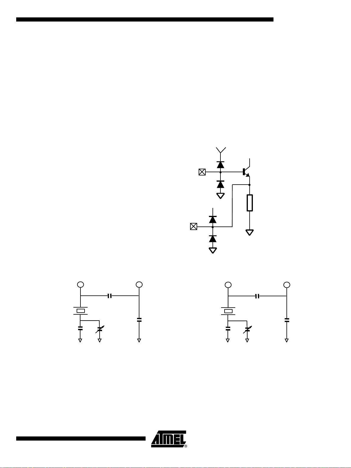
Crystal Reference Oscillator The reference cloc k i s based on a classical Colpitts architecture with three external
capacitors.
An XTAL with load capac itor in the range of 10 pF - 20 pF is recommended. The bias
circuitry of the oscillator is optimized to produce a low drive level for the XTAL. T his
reduces XTAL aging. Any standard, parallel mode 10.245 MHz or 20.945 MHz crystal
canbeused.
Note: The PLL is activated only when the o scillator is stabilized.
Figure 5. Crystal Oscillator Inputs
XTAL1
XTAL2
Figure 6. Typical Networks
(2)
XTAL2
C2 = 56 pF
CL = 20 pF
(1)
33 pF
XTAL1
C1 = 68 pF
6.5/30 pF
XTAL2
C2 = 68 pF
(2)
XTAL1
C1 = 82 pF
CL = 16 pF
Notes: 1. Various load capacitance (CL) crystals can be used. In case CLdiffers of 16 pF or 20 pF, the surrounding network (C1, C2)
2. Thanks to the fine steps of the synthesizer (200 Hz), the trimmer capacitor can be replaced by a software adjustment.
(1)
15 pF
must be re-calculated.
6.5/30 pF
Synthesizer A high-speed, high-resolution multi-loop synthesizer is integrated. The synthesizer can
operate within two frequency bands: 400 MHz to 480 MHz and 800 MHz to 950 MHz. All
channels in these two bands can be selected through software programming (registers
F0 to F3). All circuitry is on-chip with the exception of the PLL loop filter. The phase
comparison is made thanks to a charge pump topology. Typical charge pump current is
225 µA.
1942C–WIRE–06/02
7
Page 8
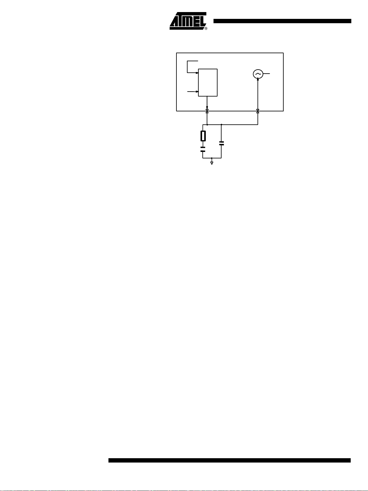
Figure 7. Synthesizer Loop Filter Schematic
P F D
&
C H P
Fref
VCO
FILT1
Note: The PLL loop filter can be designed to optimize the phase noise around the carrier.
Three configurations can be suggested, regarding the application and channel spacing:
- Narrow band: (14.7 kΩ + 2.2 nF) // 220 pF
-Typical:(3.3kΩ + 5.6 nF) // 560 pF
- High datarates: (10 kΩ + 1 nF) // 100 pF
VCOIN
8
AT86RF211
1942C–WIRE–06/02
Page 9
Receiver Description
)
Figure 8. Typical Expected Currents in Rx Mode
32.00
AT86RF211
Supply Current - R x Mode
868 or
915 MHz
30.00
Isupply (mA)
28.00
26.00
2.25 2.50 2.75 3.00 3.25 3.50 3.75 4.00 4.25
Vsupply (V)
Detailed Current - Rx Mode
10.00
8.00
6.00
4.00
Suppl y Currents (mA
2.00
0.00
2.25 2.50 2.75 3.00 3.25 3.50 3.75 4.00 4.25
Vsupply (V)
433 MHz
EVCC2
EVCC1
RXVCC
CVCC2
CVCC1
AVCC
DIVCC
IF2VCC
TXVCC
1942C–WIRE–06/02
9
Page 10
Overview and Choice of Intermediate Frequencies
For selectivity and flexibility purpose, a classical and robust 2 IF superheterodyne architecture has been selected for the AT86RF211. In order to minimize the external
components cost, the most popular IF values have been chosen. The impedances of the
input/output o f the mixing s tages have been internally matched to the most usual
ceramic filter impedances.
Two typical IF values are suggested:
• 10.7 MHz is the most popular option.
• 21.4 MHz: the image frequency is far enough from the carrier frequency to enable
the use of a front-end ceramic filter instead of a SAW filter. It is also noticeable that
21.4 MHz quartz filters usually have more abrupt slopes than 10.7 MHz ceramic
filters.
Rx - Tx Switch A S PST switch is integrated. In the transmission mode, it protects the LNA input from
the large voltage swings of the PA output (up to several volts peak-to-pea k) , which is
switched to a high impedance state. It is automatically turned ON or OFF by the RX/TX
control bit. The insertion loss is about 2 dB and the reverse isolation about 30 dB i n a
300Ω environment.
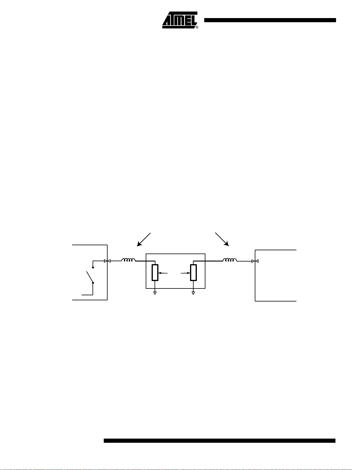
Image Rejection and RF Filter The immunity of the AT86RF211 can be improved with an external band-pass filter.
For example, when using a SAW Filter, this device must be matched with the LNA input
and the switch output. The following scheme gives the typical implementation for an
868 MHz application with a 50Ω/50Ω SAW filter.
Figure 9. Typical 50Ω SAW Filter Implementation in the 868 MHz Band
These inductors can be printed
SWOUT (pin 48)
SPST Switch
SAW
50Ω
See Table 2 for precise matching information.
The SAW filter can be replaced by a TEM ceramic, helicoidal or a ceramic coax λ/4 res-
onator designed as a narrow band-pass filter. For instance, with an IF selected at
10.7 MHz, a -3 dB bandwidth of 5 MHz, with an insertion loss of 1 dB and an image
rejection of 12 dB can be achieved with the following:
12 nH2.2 nH
RXIN
(pin 45)
10
AT86RF211
1942C–WIRE–06/02
Page 11
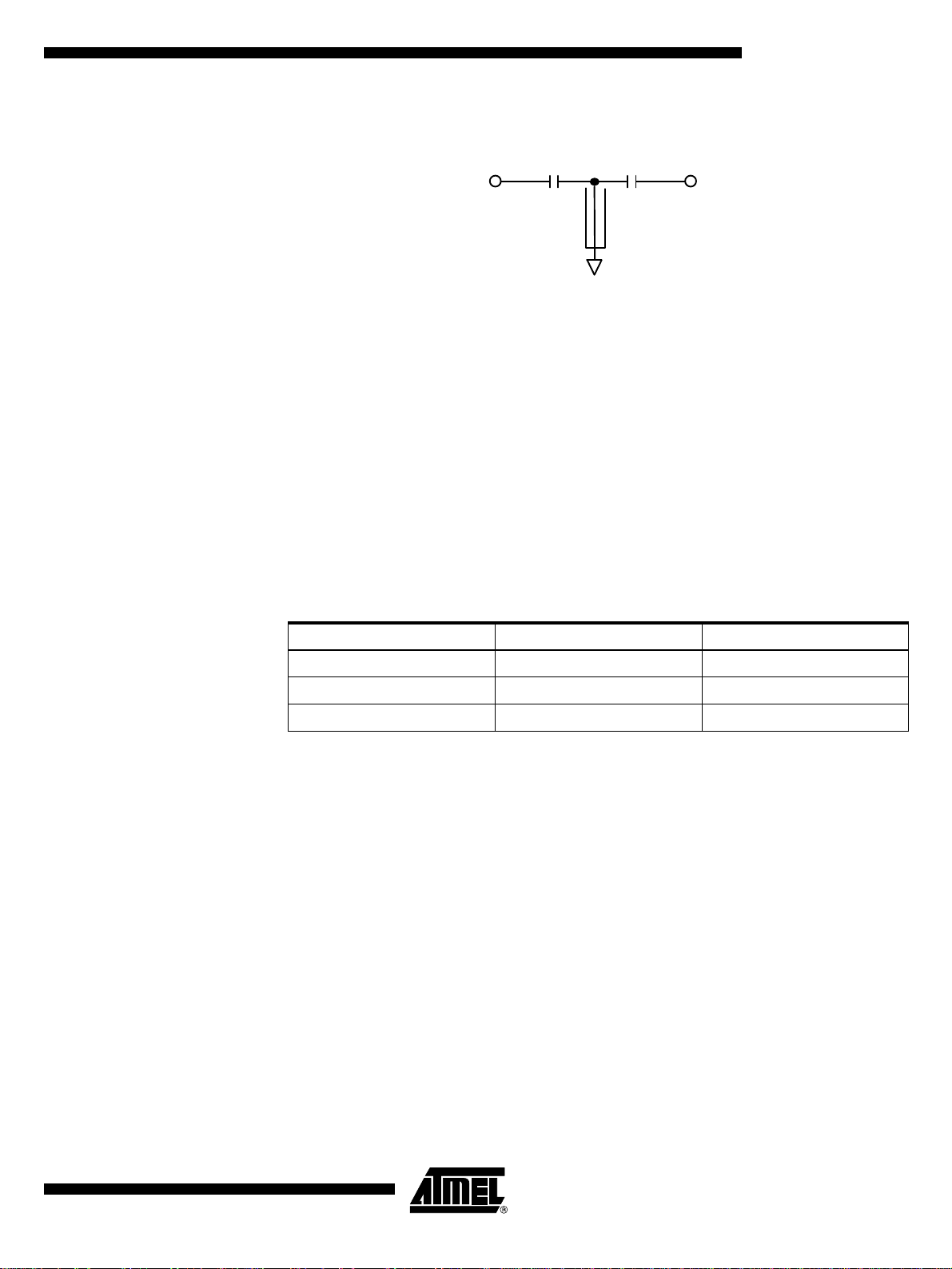
Figure 10. TEM Filter
AT86RF211
1
/4
TEM
pF
1 pF
Zc = 7Ω
l = 0.75
(19 mm)
Such a filter also p rovi des an out-of-band interference reje ction greater than 20dB,
40MHzawayfrom433MHz.
First LNA/Mixer The main characteristics of the LNA/Mixer are typically:
• Voltage gain: 17 dB for the LNA/Mixer; 11 dB if gain min. is selected
• Bandwidth: 1.2 GHz
• Noise figure of LNA alone: 3 dB at 900 MHz, best matching
• Noise figure of LNA + mixer:
8 dB at 900 MHz, with maximum gain and best matching
12 dB at 900 MHz, with minimum gain and best matching
• 1 dB compression point: -20 dBm at the input of LNA
• Matching:
Table 2. Matching Information
Frequency Band RXIN
(1)
SWOUT
(2)
433 MHz 35 + j 170Ω 24 - j 43Ω
868 MHz 37 + j 85Ω 50 - j 42Ω
915 MHz 30 + j 85Ω 50 - j 42Ω
Notes: 1. RXIN: impedance to be seen by LNA input for NF optimization purpose
2. SWOUT: output impedance of the RF switch
The gain is programmable through bit 25 of CTRL1 register (6dB attenuation when min
gain is selected). The choice for the matching between the SWITCH and the LNA
depends main ly on the chosen SAW filter. Usual ly in/out impedance o f SAW filters is
50Ω, but other ones can be implemented and the matching network recalculated thanks
to the previous impedance table.
The LNA is directly coupled to the first mixer. Input and output of the LNA/Mixer must be
connected through a capacitive link because of thei r internal DC coupling. A SAW or
ceramic filter provides such a link.
1942C–WIRE–06/02
11
Page 12
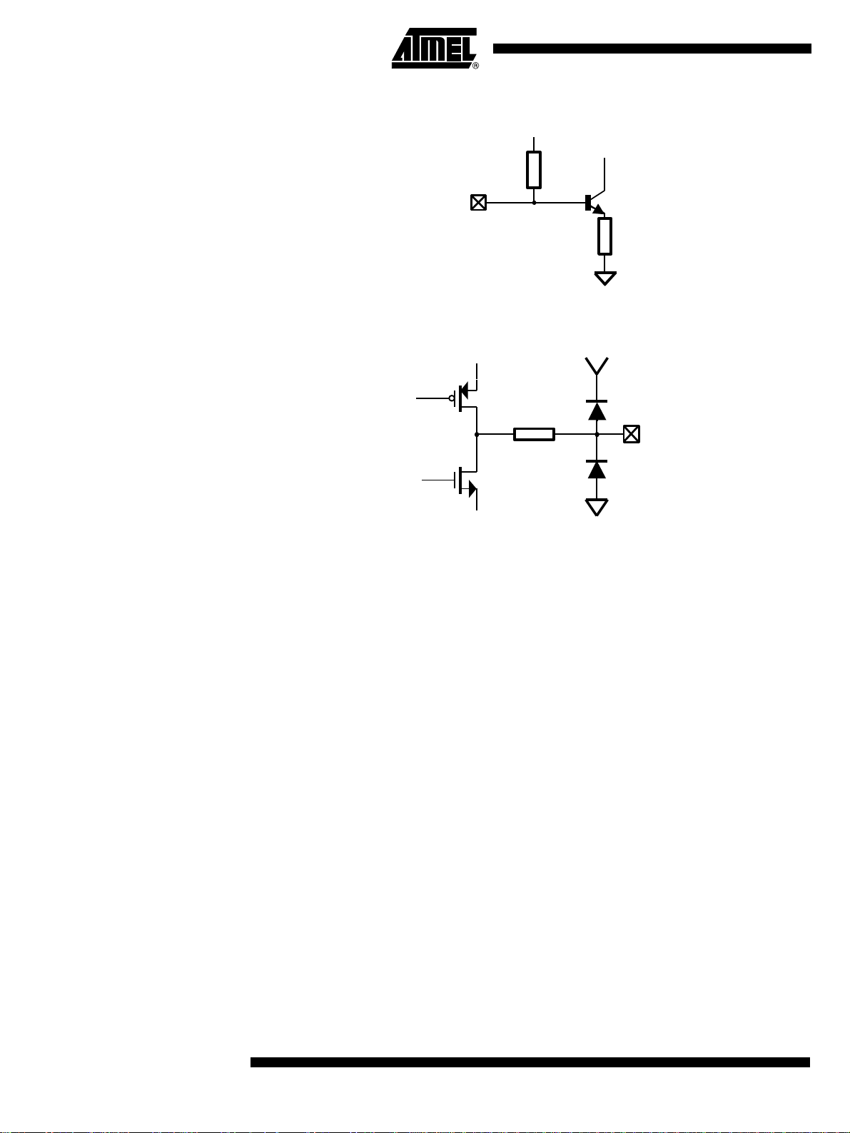
Figure 11. Schematic Input of the LNA
Figure 12. Schematic Output of the Mixer
The first mixer translates the input RF signal down to 10.7 MHz or 21.4 MHz as chosen
by the user. The local oscillator is provided by the same synthesizer which will generate
a local frequency 10.7 MHz or 21.4 MHz away from the Tx carrier frequency.
The output impedance of the mixer is 330Ω with a 20% accuracy, so that low cost, standard 10.7 MHz ceramic filters can be directly driven. Other IFs may be chosen thanks to
the high bandwidth (50 MHz) of the mixer.
IF1 filtering A popular ceramic filter is used to reject the second image frequency and provide a first
level of filtering.
The IF1 filter can however be removed; it leads to a sensitivity reduction of about 3 dB
(the substitution coupling capacitor should be > 100 pF).
IF1 Gain and Second Mixer The input impedance of the IF1 amplifier is naturally 330Ω to match the input filter. The
voltage gain, i.e. gain at 10.7 MHz or 21.4 MHz added to the conversion gain at 455 kHz
is typically 14 dB when loaded by 1700Ω. The second mixer operates at a fixed LO frequency of 10.245 MHz or 20.945 MHz. Its output impedance is 1700Ω in parallel with 20
pF.
IF1OUT
12
AT86RF211
1942C–WIRE–06/02
Page 13
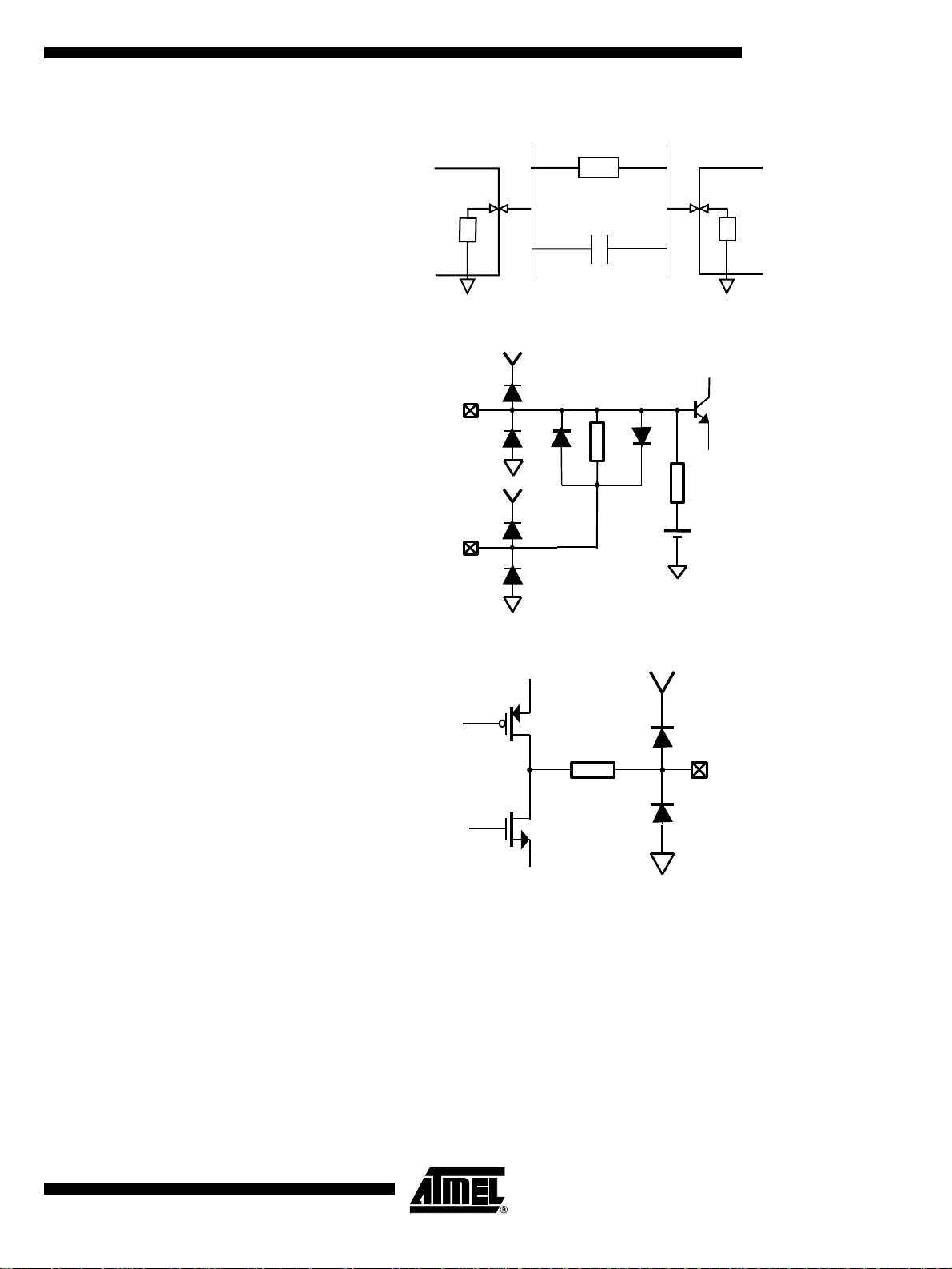
Figure 13. IF1 Filtering
IF1
AT86RF211
Filter
IF1OUT
(pin 36)
330 Ω
C > 100 pF
Figure 14. Schematic Input of IF1 Amplifier
IF1IN
IF1DEC
330Ω
IF1IN
(pin 35)
"or"
330 Ω
20 kΩ
Figure 15. Schematic Output of the Second Mixer
1600 Ω
IF2OUT
IF2 Filtering and Gain IF2 filtering achieves a narrow channel selection. In case it is not used, it should be
replaced by a > 1 nF coupling capacitor, thus the IF1 filter is the only part achieving the
channel selection. Available commercial filters with a 35 kHz BW allow data rates up to
19.6 kbps if crystal temperature drifts are very low.
For faste r communications and/or wider channelization, this ceramic filter can be
replaced by an LC band-pass filter as proposed hereafter.
1942C–WIRE–06/02
13
Page 14
Figure 16. LC Band-pass Filter
10 nF
Filter
gain
F1
F2
~ F1
40 kHz or higher
~ F2
10 nF
global response
Frequency
• 10 nF capacitors cut DC response forward and backward.
• The first network has the low cut-off frequency.
• The second network has the high cut-off frequency.
IF2 Amplifier Chain The input impedance of the IF2 amplifier is 1700Ω. This value enables the use of popu-
lar filters with impedance between 1500Ω and 2000Ω. It is directly connected to the FSK
demodulator. The bandwidth is internally limited to 1 MHz to minimize the noise before
the discriminator. It acts like a band pass filter centered at 455 kHz with capacitive coupling between stages of amplifier and mixer. Total voltage gain is typically 86 dB.
Thanks to the capacitive coupling, no slow DC feedback loop is needed enabling a fast
turn on time. IF2DEC has to be decoupled with at least 2.2 nF.
Figure 17. Input of the IF2 Amplifier Schematic
IF2IN
1900 Ω
14
AT86RF211
IF2DEC
1942C–WIRE–06/02
Page 15
AT86RF211
RSSI Output The RSSI value can be read as a 6 bits word in the STATUS register. Its value is linear
in dB as plotted below:
Figure 18. Typical RSSI output (board implementation, T = 25°C, V
CC
=3V)
RSSI Output
70
60
50
40
30
RSSI Code
20
10
0
-110 -100 -90 -80 -70 -60 -50 -40 -30
Note: Should the RSSI be required for accuratemeasurement purpose (precision better than 5 dB), then it is possible to measure one
value with a calibrated RF source and store it into the microcontroller, during the production testing.
Di spersi on: +/-5 dB
Dynamic Range: 50dB
Power Level at Antenna Input Port (dBm)
The RSSI dynamic range is 50 dB from -95 dBm to -45 dBm RF input signal power, over
temperature and power supply ranges. The RSSI LSB’s value weighs about 1.3 dB i n
the linear area. The RSSI value is measured from the IF2 chain.
The RSSI is periodically measured thanks to a successive approxi mati on ADC with a
12 µs clock. Thereafter, the time needed to complete the right code depends on the
power step: a 10 dB step on the aerial leads to a 10/1.3 = 8 clock cycles, i.e. 96 µs (full
range from code 0 to 63 = 756 µs). Its value can be compared with a user predefined
value (TRSSI), so that the demodulated data is enabled only if the RSSI value is above
this threshold. Some hysteresis effect may be added (see CTRL1 register’s content).
The AT86RF211 also has the possibility to measure another voltage. The ADC measuring the RSSI can be turned into voltage or discriminator output DC level measurement.
1942C–WIRE–06/02
15
Page 16

Figure 19. ADC Converter Input Selection
STATUS register
RSSI
M
Vcc supply
DISCOUT
(MOFFSET)
Note: For voltage measurement, the LSB weighs 85 mV and the reference voltage is 1 .25V.
M
Voltage
U
X
CTRL1[1]
U
X
The ADC measuring the RSSI can be turned into voltage or discriminator output DC
level measurement.
FSK Demodulator Its structure is based on an oscillator:
Figure 20. Schematic of the FSK demodulator
Fin
RBW
CTRL1[24]
oscillator
ADC
MRSSI
M
U
X
MVCC
A
F
D
The oscillator’s natural frequ enc y is F
B
and it actua ll y oscillates at the Fin frequency.
D
C
The signal at the output of the oscillator (point A) is proportional to the frequency difference between Fin and F
. The XOR function translates the difference into a pulse duty
D
cycle (point B).Thereafter by low-pass filtering of the signal is obtained a mean voltage
of the signal (point C).
The architecture of this demodulation is thereby analog and allows the transmission of
continuous data str eam of the same value as the output voltage is pro portional to the
input frequency. Thus it is not mandatory to use Manchester encoding and the first bit is
correctly demodulated.
The oscillator feedback resistor controls the center frequency F
.Itisadjustedaccord-
D
ing to the output of a dummy FSK demodulator driven by a 455 kHz internal reference
frequency which is a division of the reference crystal. The discrete components connected to pin 32 DISCFILT are the loop filter of the PLL stabilizing the 455 kHz signal.
16
AT86RF211
1942C–WIRE–06/02
Page 17

AT86RF211
The input RBW resistor controls the discriminator bandwidth. This bandwidth is selected
by CTRL1[6]. The default value is "standard discriminator BW". The slope of the discriminator increases by 5 mV/kHz/V with V
Example:
V
= 3V implies +17 mV/kHz sensitivity for the demodulator
CC
V
= 3.6V implies +20 mV/kHz sensitivity for the demodulator
CC
Data Slicer The analog signals at the output of the discriminator (DISCOUT, pin 27) are converted
into CMOS level data by a high resolution comparator called a Data Slicer.
The Data Slicer has a reference for its comparator which can be chosen thanks to
CTRL1[4]. The reference sets the comparison level of the comparator. One option is to
extract the average value of the demodulated signal on the SKFILT pin (25), this is the
external mode. The other option is to set an absolute value for this reference (internal
mode).
• External mode:
The external mode uses the average value of the demodulated signal as the compari-
son level for the comparator. Thus there must be enough transitions in the message to
ensure that the average value remains between the "0" level and the "1" level. Manchester encoding can be used in this mode as well as DC-free encoding schemes. The
choice for SKFILT capacitor is a trade-off between the maximum duration of a constant
bit (whatever "0" or "1") and the max allowed settling time to charge this capacitor after
powering up.
Note: The SKFILT pin is in high impedance state during the "sleep" period of the Wake Up
mode, so that the level is kept constant and there is no need to charge again this tank.
andis14mVat2.4V.
CC
• Internal mode:
The internal mode uses the output of a DAC as the comparison level. Once this thres-
hold has been correctly set, an "absol ute" data slicing of the demo dulated signal is
possible: no need for DC-free modulation scheme (it is possible to send a "0" or "1"
infinitely).
Figure 21. Schematic of the Data Slicer
DISCOUT
DSIN
SKFILT
DATAMSG
+
-
Choice of internal or
external reference for
the data slicer
+
-
+
Vdd/2
+
-
4 bits
+
Σ
100 kΩ
1942C–WIRE–06/02
17
Page 18

To operate this way, the user must make sure that the "0" and "1" level at the output of
the discriminator are "on both sides" of the comparison level in order for the decision to
be made properly.
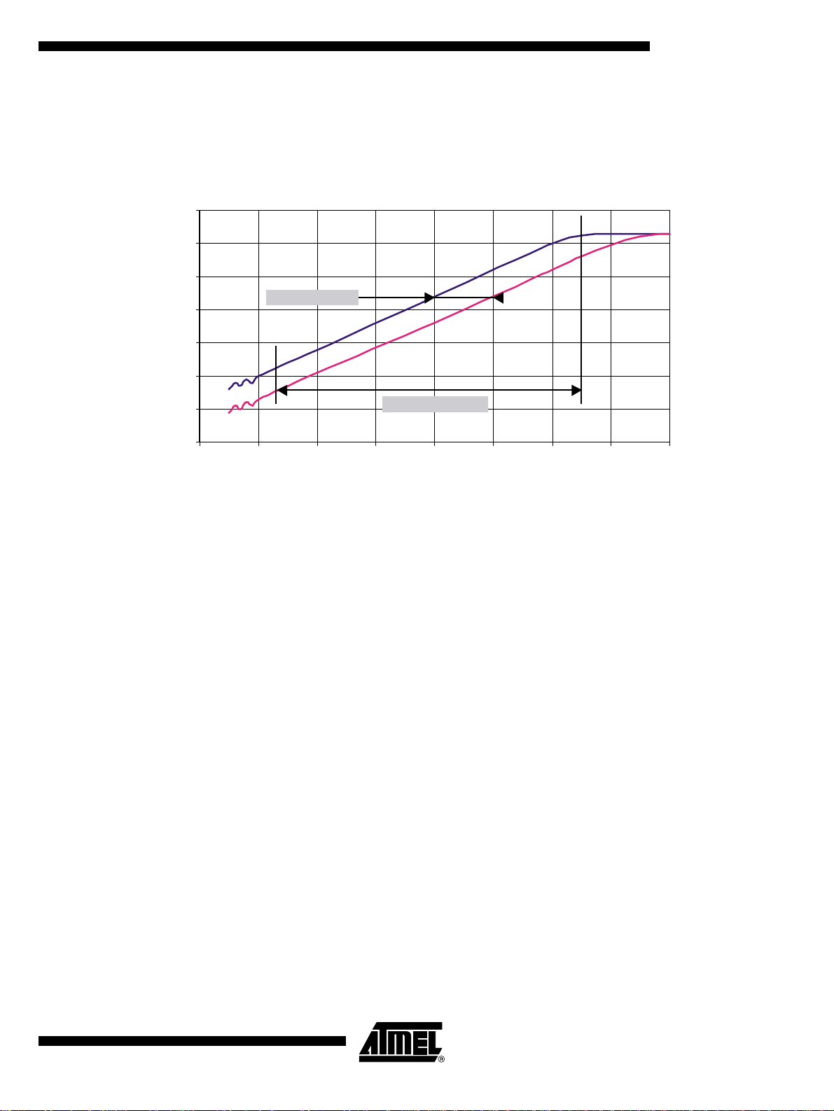
Figure 22. HowtoSetUptheDataSlicingParameters
DISCOUT:
demodulated
data
Not OK
Comparator threshold
OK
Time
To set the discriminator and the Data Slicer accordingly:
– It is possible to measure the output DC level of the discriminator DISCOUT
(thanks to the A/D embedded converter)
– DTR[1:0] make it possible to shift (up or down) the DC level at the output of
the discriminator :
- DTR[1] = 1: +180 mV + 77x (V
- DTR[0] = 1: -180 mV - 77x (V
– DTR[5:2] make it possible to tune the comparison threshold around V
16 levels are possible, with a LSB = 15 mV per Volt of supply voltage. V
CC
CC
-2.4V)
-2.4V)
CC
/2.
CC
/2
corresponds to DTR[5:2] = 0111, and the RESET value is 1000.
These procedures can be made automatically by software. Please refer to the application note.
18
AT86RF211
1942C–WIRE–06/02
Page 19

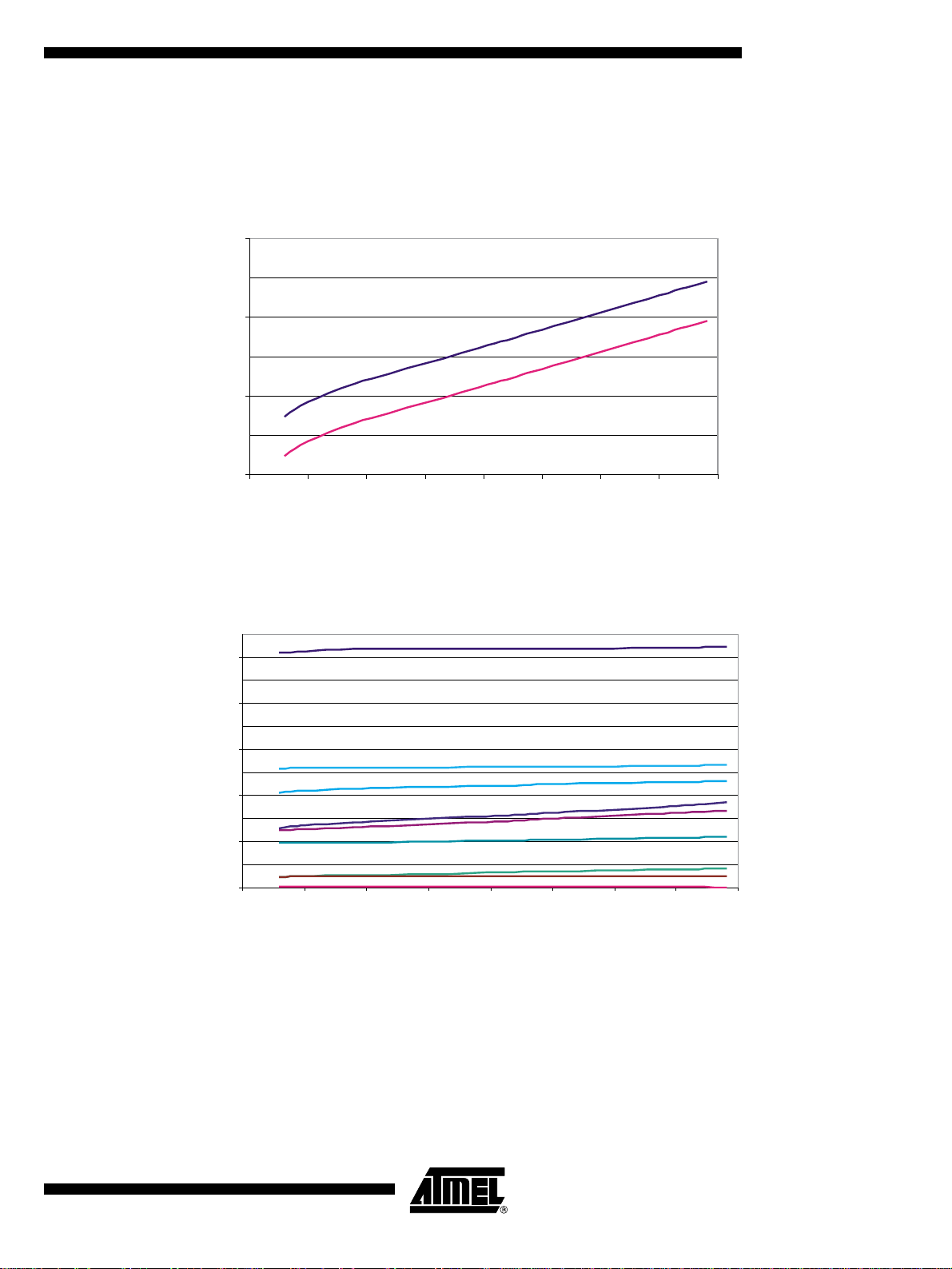
Transmitter Description
)
Figure 23. Typical Expected Currents in Tx Mode
Supply Current - Tx Mode
AT86RF211
65.00
60.00
55.00
50.00
45.00
40.00
35.00
Isupply (mA)
30.00
25.00
20.00
15.00
2.25 2.50 2.75 3.00 3.25 3.50 3.75 4.00 4.25
Vsupply (V)
Detailed Current - Tx Mode
30.00
25.00
915MHz
868MHz
433MHz
PA
20.00
TXVCC
15.00
10.00
Suppl y Currents (mA
5.00
0.00
2.25 2.50 2.75 3.00 3.25 3.50 3.75 4.00 4.25
Vsupply (V)
EVC C2
CVCC2
CVCC1
RXV CC
1942C–WIRE–06/02
19
Page 20

Power Amplification The Power Amplifier has been built to deliver more than +10 dBm, i.e. 10 mW in the
three popular frequency bands. This power level is intended to be measured on the
aerial port with a correct output matching network. Note that a correct calculation of the
matching network guarantees an optimal power efficiency.
Naturally, the greater the PA output voltage swing, the better the power efficiency. As
the PA output is supplied through an inductor, a swing of 2 x V
due to saturation effects, the voltage s wing is limited to approximatel y (2 x V
is possible. In practice,
DD
DD
)-1V.
With a power supply voltage of 3V, the PA output voltage is 5V peak-to-peak, or
1.77 V
EFF
.
Figure 24. Output of the Power Amplifier
The PA must be correctly matched to deliver the best efficiency in terms of output power
and current consumption. Here is an example of the typical recommended output network in the 868 MHz band:
Figure 25. Output Matching at 868 MHz
Power supply
filtering
Vcc
Supply
12 nH
RF
PA output
Note: The filter is designed to meet relevant regulations. Please refer to application note for details.
1.5 nH
inductor
~ 50Ω matched filtering
50Ω
A benefit of this network is to filter the output signal harmonic levels; hence it can be
designed to meet a particular regulation.
It is mandatory to implement low impedance grounding techniques. Excessive inductor
values to ground will not only limit the PA output voltage swing, but may also trigger RF
instability. Board design is vital to avoid parasitic loss when high output power is needed
(direct short connection to a single low impedance ground plane).
aerial
20
AT86RF211
1942C–WIRE–06/02
Page 21

AT86RF211
An automatic level control loop (ALC) is integrated, in order to minimize the sensitivity of
the PA to the temperature, process and power supply variations. For instance, at +85°C,
the output power is about 2 dB less than at 25°C. At -40°C, the output power is higher
than at 25°C. The ALC is controlled by a current which is generated in the following way:
Figure 26. ALC of the Power Amplifier
(v)
1.25 V
Figure 27. Typical Output Power of the PA for T = 25°CandV
Output Power
14
12
10
8
6
Pout (dBm)
4
ref
=
Ω
R
POWER
V
3 bits
digital
power control
433MHz
868MHz
DAC
915MHz
I
OUT
To ALC
i
U
I
R
POWER
18 k
≅
=3V
CC
2
0
-2
26 31 36 41 46 51 56 61
Isupply (mA)
Hardware Control The max output power is dete rmi ned by R
obtained with R
POWER
=10kΩ.
18 kΩ is the nominal value for a +10 dBm output in the 868 MHz frequency band.
Decreasing this value to 10 kΩ will lead to +14 dBm at 433 MHz, +12 dBm at 868 MHz,
+10 dBm at 915 MHz (typical values for conducted output power).
1942C–WIRE–06/02
POWER
and the maximum output power is
21
Page 22

Figure 28. R
Input Schematic
POWER
100 Ω
Note: Keeping the PA output matched guarantees maximum power efficiency.
R
POWER
Software Control The power can then be adjusted, from the value set by R
12 dB below, by programming the bits 6 to 8 of the CTRL1 register. So, 8 levels are digitally selectable w ith a variation of the output power. The minimum r egulated output
power is set to -10 dBm.
Table 3. Software Control of the Power Level
Pout at 433 MHz
TXLVL (CTRL1)
000 0 -2 -3
001 4 0 0
010 6 3 2
011 8 5 4
100 10 7 5
(dBm)
Pout at 868 MHz
(dBm)
down to a maximum of
POWER
Pout at 915 MHz
(dBm)
101 11 8 7
110 12 9 8
111 13 10 9
Note: Unless otherwise specified, typical data given for R
=18kΩ,T=25°C, VCC=3V
POWER
Control Logic
Serial Data Interface The application microcontroller can control and monitor the AT86RF211 through a syn-
chronous, bidirectional, serial interface made of 3 wires:
• SLE: enable input
• SCK: clock input
• SDATA: data in/out
When SLE = ‘1’, the interface is inhibited, i.e. the SCK and SDATA (in) values are not
propagated into the IC, reducing the power consumption and preventing any risk of parasitic write or read cycle.
A “read” or “write” cycle starts when SLE is set t o ‘0’ and stops when SLE is set to ‘1’.
Only one operation can be performed in one access cycle: only one register can be
either read or written.
22
AT86RF211
1942C–WIRE–06/02
Page 23

AT86RF211
• Register Interface Format
A message is made of 3 fields:
– address A[3:0]: 4 bits (MSB first)
– R/W: read/write selection
– data D[31:0]: up to 32 bits (MSB first)
ADDRESS R/W DATA up to 32 bits (variable length)
A[3] A[2] A[1] A[0] R/W MSB D[nbit-1:0] LSB
Variable register length and partial read or write cycles are supported.
In case of partial read or write cycles, the first data (in or out) is always the MSB of the
register.
•
WRITE Mode (R/W = 1)
The address, R/W and data bits are clocked on the rising edge of SCK.
If the number of data bits is lower than the register capacity, the LSB bits keep their
former value allowing safe partial write. If the number of data bits is greater than the register capacity, the extra bits are ignored.
The data is actually written into the register on the rising edge of SLE when the data
length is less or equal to the register length.
When trying to write more data than the register length, data field is written on the first
extra rising clock edge regarding register length.
Figure 29. Write Chronogram: Complete Write Cycle in a 10 bits Register
SLE
SCK
SDATA
A[3] R/W
A[1]A[2]
D[8]
D[7]
D[6] D[5] D[4] D[3] D[2] D[1] D[0]A[0] D[9]
The complete register of 10 bits is updated on a rising edge of SLE.
Figure 30. Write Chronogram: Partial Write Cycle, Writing 2 bits
SLE
1942C–WIRE–06/02
SCK
SDATA
A[0] D[31]
A[1]A[2]A[3]
R/W
D[30]
23
Page 24

Only t he 2 MSBs are upda ted on the rising e dge of SLE; other register bits are
unchanged.
READ Mode (R/W = 0)
•
The address and R/W bits are clocked on the rising edge of SCK.
The data bits are changed on the falling edge of SCK. The MSB of the register is the first
bit read.
SDATA I/O pin is switched from input to output on the edge following the "1" clocking the
R/W bit.
It is possible to stop reading a register (SLE back to “1”)atanytime.
If an attempt to read more bits than the register capacity is detected, SDATA is clamped
to “0”.
If the address of a register is not valid, SDATA is set to “1” during the first 32 SCK peri-
ods, then to “0” during all the extra periods.
SDATA is switched back to the input state when SLE is back to “1”.
Figure 31. Read Chronogram: Complete Read Cycle from a 10 bits Register
SLE
SCK
SDATA
direction
A[2
]
INPUT OUTPUT INPUTSDATA
A[0]
R/W
D[9
D[8]A[1]
]
D[7]A[3]
Figure 32. Read chronogram: Partial Read Cycle, Reading 2 bits
SLE
SCK
SDATA
SDATA
mode
INPUT
A[0] D[31]A[1]A[2]A[3]
D[6] D[5] D[4] D[3] D[2] D[1] D[0]
R/W
D[30]
OUTPUT INPUT
24
AT86RF211
1942C–WIRE–06/02
Page 25

Figure 33. Chronogram with Timing
AT86RF211
SLE
SCK
SDATA
direction
tdle
T tw
thdtsd tpzon tpd tpzd
A[3] R/W
A[2
]
INPUT OUTPUT INPUTSDATA
A[0]A[1]
tw
D[9]D[8] D[7] D[6] D[5] D[4] D[3] D[2] D[1] D[0]
tdle
Note: For the timing specification, please refer to the timing table “Digital CMOS DC Characteristics” on page 42.
Registers
Table 4. Registers Overview
Name Address A[3:0] Nbits Read-Write Comments
F0 (0000)
F1 (0001)
F2 (0010)
F3 (0011)
CTRL1 (0100)
STAT (0101)
DTR (0110)
WUC (0111)
WUR (1000)
WUA (1001)
WUD (1010)
RESET (1011)
- (1100)
- (1101)
- (1110)
CTRL2 (1111)
2
2
2
2
2
2
2
2
2
2
2
2
2
2
2
2
Note: All the registers must be reprogrammed after the voltage supply has been removed, otherwise they will be in the default state
32 R-W F0 Frequency Code
32 R-W F1 Frequency Code
32 R-W F2 Frequency Code
32 R-W F3 Frequency Code
32 R-W Main Control Register
31 R Status Register
6 R-W Data Slicer Reference/Discriminator offset adjusting
32 R-W Wake-up Control Register
18 R-W Wake-up Data Rate Register
25 R-W Wake-up Address Register
32 R Wake-up Data Register
1WReset
Reserved
Reserved
Reserved
32 R-W Control Register (Lock Detect - Clock Recovery)
1942C–WIRE–06/02
25
Page 26

Reset Register (RESET)
Name RESET
nbit 0
Writing in this register (0 or 1) triggers an asynchronous reset. This register can only be
written.
All registers return to reset s tate. The chip r eturns i n power-down. So all the following
blocks are reset:
• All registers to default value
• Wake-up function.
• Clock recovery function.
And with the power-down state, reset is applied to the following blocks:
• Synthesizer dividers.
• Clock recovery function.
• PLL lock detect.
• From powering up the supplies, it takes about 10 µs or at least 1.8V before the reset
state is established (Power-on Reset).
• From reseting the device, one should wait about 10 µs before re-programming
• RSSI detection block.
• Discriminator clock (455 kHz).
Control Register (CTRL1)
Table 5. CTRL1 Overview
Name PDN RXTX DATACLK TXLOCK PAPDN WUEN LNAGSEL MVCC TRSSI HRSSI
nbit 31 30 29 28 27 26 25 24 23-18 17-15
init 0 0 0 1 0 0 0 0 (000000)
Name TXLVL TXFS - RXFS XTALFQ FSKBW FSKPOL DSREF - - MOFFSET -
nbit 14-12 11 10 9-8 7 6 5 4 3 2 1 0
init (000
)
2
00(10
Register reset value = (10000270
)
16
)
2
01110000
2
(000)
2
26
AT86RF211
1942C–WIRE–06/02
Page 27

AT86RF211
Table 6. CTRL1 Detailed Description
(1)(2)(4)(3)
Number
Name
of Bits Comments
PDN 1 General power-down
0: power down mode; only the serial interface is active
1: AT86RF211 activated
RXTX 1 Reception or transmission selection
0: Rx mode
1: Tx mode
DATACLK 1 DATA clock recovery selection
0: no signal on DATACLK output pin
1: Clock recovery active: DATACLK activated
TXLOCK 1 Transmission on PLL lock
0: transmission enabled, regardless of the PLL lock status
1: transmission only when the PLL is locked
note: the PLL status is stored in the PLLL bit of the STATUS register
PAPDN 1 Power amplifier power down
0: Tx Power Amplifier power down mode
1: Tx Power Amplifier activated (only if PDN = 1)
resetvalue:0
resetvalue:0
resetvalue:0
resetvalue:1
resetvalue:0
WUEN 1 Wake-up function enable
0: Wake-up function disabled, whatever the content of the wake-up control registers
1: Wake-up function activated, depending on the content of wake-up control registers
LNAGSEL 1 LNA gain selection
0: maximum gain
1: minimum gain
MVCC 1 RSSI or V
power supply measurement selection
CC
0: RSSI voltage measurement, value is stored in STAT register: MRSSI bits
1: V
voltage measurement, value is stored in STAT register: MVCC bits
CC
TRSSI 6 RSSI value threshold
DATAMSG validated if RSSI ≥ TRSSI + HRSSI (high RSSI level)
DATAMSG inhibited if RSSI < TRSSI - HRSSI (low RSSI level)
HRSSI 3 Value RSSI hysteresis
TXLVL 3 Tx PA output power selection
(000)
: minimum transmission level
2
: maximum transmission level
(111)
2
TXFS 1 Tx frequency selection
0: F0 & F1 1: F2 & F3
resetvalue:0
resetvalue:0
resetvalue:0
reset value: (000000)
reset value: (000)
reset value: (000)
resetvalue:0
2
2
2
1942C–WIRE–06/02
27
Page 28

Table 6. CTRL1 Detailed Description
(1)(2)(4)(3)
(Continued)
Number
Name
of Bits Comments
– 1 reserved, must be kept to reset value: 0
RXFS 2 RX frequency selection
:F0 (10)2:F2
(00)
2
: F1 (11)2:F3
(01)
2
XTALFQ 1 Crystal frequency
0: 10.245 MHz (when IF1 = 10.7 MHz)
1: 20.945 MHz (when IF1 = 21.4 MHz)
FSKBW 1 Discriminator range
0: Narrow Discriminator BW
1: Standard Discriminator BW
FSKPOL 1 Polarity of DATAMSG
0: inverted signal
1: direct signal
DSREF 1 Data Slicer reference voltage
0: external reference: SKFILT pin voltage
1: internal reference: DAC level voltage
reset value: (10)
resetvalue:0
resetvalue:1
resetvalue:1
resetvalue:1
2
– 1 reserved, must be kept to reset value: 0
– 1 reserved, must be kept to reset value: 0
MOFFSET 1 0: internal ADC sets to V
measurement
CC
1: internal ADC sets to DISCOUT DC level measurement
resetvalue:0
– 1 reserved, must be kept to reset value: 0
Notes: 1. The same ADC is used to measure RSSI or VCCvoltage. When the VCCvoltage is measured, the RSSI measurement is
stopped (previously measured RSSI is kept into STATUS Register). This can disturb the reception process (if a threshold is
used for DATAMSG validation).So, it is not recommended to measure V
2. V
3. While in V
measurement c an not be done when the AT86RF211 is in power-down mode.
CC
measurement, it is possible to measure the DC output of the discriminator.
CC
in reception mode.
CC
4. Description of RSSI measurement with hysteresis mechanism: if the RSSI measurement is higher than the high RSSI level,
DATAMSG is validated (high RSSI level = TRSSI + HRSSI). If the RSSI measure is lower than the low RSSI level, DATAMSG is inhibited (low RSSI level = TRSSI - HRSSI). Between these two levels, DATAMSG validation depends on the
previous measurement.
Example:
TRSSI = 32 and HRSSI = 4 implies High RSSI level = 26 and Low RSSI level = 28
MRSSIsequence27323536353229282725
RSSI level NOK NOK NOK OK OK OK OK OK NOK NOK
DATAMSG valid valid valid valid valid
28
AT86RF211
1942C–WIRE–06/02
Page 29

AT86RF211
Control Register (CTRL2)
Table 7. CTRL2 Overview
Name DATARATE DATATOL LDCK N0LD1 N1LD2
nbit 31-18 17-10 9 8-5 4-0
init (0000)
16
Register reset value = (00000057)
16
(00)
16
0 (0010)
Table 8. CTRL2 Detailed Description
Number of
Name
DATARATE 14 Received DATAMSG rate
DATATOL 8 Tolerance for DATACLK, clock recovery
LDCK 1 Clock frequency is doubled to increase precision of PLL lock detection
N0LD2 4 PLL unlock condition trigger
N1LD2 5 PLL lock condition trigger
bits Comments
This value must be programmed to have the DATACLK activated.
(selected with DATACLK bit in CTRL1 register).
Value from 1 kbps to 50 kbps
Recommended value = 2% of the rate.
0: 10 MHz clock frequency
1: doubled clock frequency
Recommended values are reset values
Recommended values are reset values
• Clock Recovery Function
2
(10111)
reset value: (0000)
reset value: (00)
reset value: (0010)
reset value: (10111)
2
reset value: 0
16
16
2
2
1942C–WIRE–06/02
The clock recovery function is activated by setting to ‘1’ the DATACLK bit of the CTRL1
register.
The clock recovery function provides on DATACLK pin the data clock, synchronized on
the received data flow. The targeted position for the rising edge of the clock is the middle of the data bit. It is then easy for the microcontroller to read without synchro troubles.
Clock rec overy mechanism is based on the gene ratio n of a bas ic data clock with a
period given by DATARATE of CTRL2 with a step of about 100 ns. This basic clock is
synchronized on the received data flow with a phase correction step fixed by DATATOL
of CTRL2 register (step of about 100 ns also).
So, DATATOL can
– compensate for the difference between the read data rates from transmitter
and receiver (fixed by DATARATE).
– allow fast initial synchronization of data clock, avoiding bit transition times
and converge toward the middle of the bit.
– keep the right data rate (no additional and no removed bit) when a noisy
data with bad bit transition position arrives.
The best value of DATATO L is a trade-off between these considerations. T he typical
recommended value of RATETOL is 2% of DATARATE.
29
Page 30

Figure 34. Clock Recovery
If the tolerance is too high, the rate value is reached earlier, and the rate value could be
unstable (too big step).
If the tolerance is too low, it could be difficult to catch up the DATA and the function
could get lost.
Notice that maximum acceptable distance between two data transitions depends on the
precision of DATARATE versus transmitter actual data rate.
Synchronization mechanism is explained with the chronogram hereafter. The synchronization is done for the first bit. In worst case conditions, when data and clock arrive at the
same time, it begins at the second bit. Notice that the DATACLK signal is available as
soon as the DATACLK bit is programmed, whatever the state of DATAMSG pin.
The programmed data rate allows the creation of a basic clock at the programmed DATARATE frequency at the beginning of the reception. Then, the clock is shifted if
necessary from the t ol e ra nc e value, depe n di n g on the pr ev i o us DATA transi ti o n: the
clock is moved later or sooner, depending on the gap between CLOCK and DATA.
For example:
if DATARATE = 50 kbps, which is equivalentto a durationo f 200 x T for 1 bit, with
T = 100 ns = base clock period.
if DATATOL = 2% x DATARATE = 4 x T.
DATAMSG
DATACLK
200T
•
DATARATE Programming
Tol = 4T
Synchronized values with DATAMSG
Tol = 4T
Expected
valueExpected value
This value must be programmed only when the DATA clock is needed on DATACLK
output pin of the chip.
The DATA rate can be programmed from 1 kbps to 64 kbps with 14 bits of CTRL2
register.
DATARATE is the period of the data rate and can be pr ogrammed with a resolution
given by the crystal oscillator period:
• 10.245 MHz oscillator, period = T = 97.6 ns
• 20.945 MHz oscillator, period = T = 95.5 ns
Some datarate values with the 10.245 MHz oscillator given for example:
DATARATE[13:0] Rate Period
(160)
(205)
(vv)
10
(534)
(1024)
10
10
10
10
64 kbps 1 bit ~ 160 x T
50 kbps 1 bit ~ 205 x T
…… 1bit~vvxT
19.2 kbps 1 bit ~ 534 x T
10 kbps 1 bit ~ 1024 x T
30
AT86RF211
1942C–WIRE–06/02
Page 31

DATARATE[13:0] Rate Period
AT86RF211
(1067)
(2135)
(4269)
(10246)
10
10
10
10
9.6 kbps 1 bit ~ 1067 x T
4.8 kbps 1 bit ~ 2135 x T
2.4 kbps 1 bit ~ 4269 x T
1 kbps 1 bit ~ 10246 x T
• Datatol Programming
The tolerance for the extraction of DATA rate must be nearly 2% of the RATE. The tolerance represents the step for the calculation of the rate.
If the tolerance is too high, rate value is reached earlier but the rate value could be
unstable (step too big).
If the tolerance is too low, it could be difficult to catch up the DATA and the clock recovery could get lost.
Some tolerance values given for example, with tolerance = 2% x DATARATE:
DATATOL[7:0] Rate Period
(3)
10
(4)
10
(vv)
(20)
(21)
(43)
(85)
(205)
10
10
10
10
10
10
64 kbps 1 bit ~ 3 x T
50 kbps 1 bit ~ 4 x T
…… 1bit~vvxT
10 kbps 1 bit ~ 20 x T
9.6 kbps 1 bit ~ 21 x T
4.8 kbps 1 bit ~ 43 x T
2.4 kbps 1 bit ~ 85 x T
1 kbps 1 bit ~ 205 x T
1942C–WIRE–06/02
•
PLL Lock Detect
The PLL lock function uses UP and DOWN signals from the internal phase detector.
These signals are analyzed synchronously with a clock frequency, depending of LDCK
bit programming (10 MHz or 20 MHz sampling).
LDCK is set to ‘1’ to double the clock frequency of the function PLL lock detect, to
increase the precision of the function.
N0LD2 triggers the unlock condition of the PLL.
N0LD2 = number of consecutive edges of the sampling clock with UP and DOWN active
before considering PLL unlocked.
This value must not be set to 0 or 1. The recommended value is default value, i.e. 2.
N1LD2 triggers the lock condition of the PLL.
N1LD2 = number of cycle at the PLL reference frequency, without any unlock condition
before considering PLL locked.
This value must not be set to 0.
It is recommended to use default values indicated in the table.
31
Page 32

Frequency Registers
Table 9. Frequency Registers
Name F0, F1, F2, F3
nbit 31-0
Number
Name
F0 32 Frequency code value F0
F1 32 Frequency code value F1
F2 32 Frequency code value F2
F3 32 Frequency code value F3
Note: 1. F0, F1, F2 and F3 registers must be programmed before using the device.
of bits Comments
default register in TX mode ("0" code in FSK modulation).
default register in TX mode ("1" code frequency in FSK modulation).
default register in RX mode.
There is no simple relationship between frequency registers and the exact frequency. Atmel
provides a tool to program them on a production bench.
• Frequency Registers Selection
The FSK modulation is completely integrated. Two registers have to be program me d
(default F0 and F1) to allow "0" and "1" transmission.
The frequency register selection depends on the control r egister pr ogramming and on
the DATAMSG pin:
RXTX RXFS TXFS DATAMSG Mode
0 00 X X Receive LO is F0
0 01 X X Receive LO is F1
0 10 X X Receive LO is F2
0 11 X X Receive LO is F3
1 XX 0 0 Transmit "0" on F0
1 XX 0 1 Transmit "1" on F1
1 XX 1 0 Transmit "0" on F2
1 XX 1 1 Transmit "1" on F3
32
AT86RF211
1942C–WIRE–06/02
Page 33

AT86RF211
In reception mode, only one frequency needs to be programmed. In transmission mode,
two different registers (F0 & F1), or (F2 & F3) must be programmed for “0” code and “1”
code transmission. The DATAMSG pin value actually selects the used register. The four
registers can also be set to d efine two channels, so that the AT86RF211 may switch
quickly from a channel to the other.
Mode Programmed Frequency
RX FCHANNEL ± IF1
TX FCHANNEL ± deviation
Example:
FCHANNEL = 868.3 MHz
IF1 = 10.7 MHz
Deviation = ± 4 kHz
Mode FSK
RX 868.3 ± 10.7 = 879 MHz or 857.6 MHz programmed in F2
TX 868.3 ± 0.004 = 868.304 MHz programmed in F1 when DATAMSG = “1”
and 868.296 MHz programmed in F0 when DATAMSG = “0”
Notes: 1. In reception mode, one of the two frequencies (879 MHz or 857.6 MHz) can be cho-
sen, taking into account external parameters (for example, the noise that brings the
image frequency).
2. Two frequencies are used to transmit data: 868.304 MHz for ”
868.296 MHz for ”
bit 5 of CTRL1.
0” transmission. The polarity of DATAMSG can be swapped using
1” transmission and
Status Register Th e STATUS regi ste r is used to read t he status of internal fu ncti ons (including the
wake-up function) or the output value of the internal ADC. This register can only be
read.
Table 10. Status Register Overview
Name PLLL MRSSI MVCC WAKEUP - MSGERR
nbit 30 29-24 23-18 17 16 15
Name MSGDATL MSGMRATE
nbit 14-10 9-0
1942C–WIRE–06/02
33
Page 34

Table 11. Status Register Detailed Description
Number
Name
PLLL 1 PLL Lock flag
MRSSI 6 Measured RSSI level
MVCC 6 Measured VCCpower supply voltage or discriminatoroutput when
WAKEUP 1 WAKEUP flag
-1Reserved
MSGERR 1 Wake-up message error in test message mode
of bits Comments
0: PLL unlocked
1: PLL locked
reset value: 0
reset value: (00)
MOFFSET = 1
reset value: (00)
Copy of the WAKEUP pin, but not affected by polarity selection.
0: no wake-up m essage received
1: wake-up message received
reset value: 0
reset value: 0
0: no error detected in the received message
1: message received with error
reset value: 0
16
16
MSGDATL 5 Wake-up message data length
length of the data stored in WUD (received message).
reset value: 0
MSGMRATE 10 Wake-up message measured data rate
bit period extracted from message header of the w ake-up
message.
Measured as a multiple of 1.56 µs (like RATE in WUR register).
0: 1 x 1.56 µs
(vv)
: vv x 1.56 µs
10
: 1024 x 1.56 µs
(3ff)
16
reset value: (000)
DTR Register The DTR register allows the user to precisely adjust the offset of the data slicer input.
Table 12. DTR Overview
Name DSREF[3:0] DISCHIGH DISCLOW
nbit 5-2 1 0
init (1000)
Register reset value = (20)
2
16
00
16
34
AT86RF211
1942C–WIRE–06/02
Page 35

AT86RF211
Table 13. DTR Detailed Description
Number
Name
DSOFFSET 4 Data Slicer reference tuning
DISCHIGH 1 Discriminator offset shift (high)
DISCLOW 1 Discriminator offset shift (low)
Wake-up Control Register
Table 14. WUC Overview
Name WUE DATA STOP DATL ADD – WPER WL1
nbit 31 30 29 28-24 23 22 21-13 12-6
of bits Comments
(0000)
to (1111)
2
0: no shift
1: output level increased
0: no shift
1: output level decreased
2
reset value: (1000)
2
resetvalue:0
resetvalue:0
init 0 1 1 (11111)
2
1 0 (001011111)
2
(0000100)
2
Name WL2 ISTU ––
nbit 5-3 2 1 0
init (010)
2
Register reset value = (7f8be110)
16
000
Table 15. WUC Detailed Description
Number
Name
WUE 1 Wake-up function enable
DATA 1 Data content
STOP 1 STOP field usage
of bits Comments
Returns to “0” when a valid message is received.
0: wake-up disable
1: wake-up enable
0: message without data field
1:messagewithdatafield
0: fixed data length: data length set from 1 to 32 by DATL
1: variable data length: data length given by the STOP field location; DATL must be set to (11111)
reset value: 0
reset value: 1
2
reset value: 1
1942C–WIRE–06/02
35
Page 36

Table 15. WUC Detailed Description (Continued)
Number
Name
DATL 5 Data length
ADD 1 Address content
MSGTST 1 Message error test
WPER 9 Wake-up period
WL1 7 Minimum delay before TEST1 (check of RSSI level)
WL2 3 Minimum delay between TEST 1 and TEST 2 (check of header detection)
ISTU 1 Inhibit stuff mechanism
of bits Comments
Valid in fixed data length mode (STOP = 0).
(00000)
: 1 bit (min data length value)
2
------------------(11110)
(11111)
:31bits
2
: 32 bits (max data length value)
2
0: message without address field
1: message with address field
0: no error detection mode
1: error detection enabling for debugging
Variable from 10 ms to 328 sec with an accuracy of ±20%.(on-chip RC oscillator)
Variable from 1ms to 1.024 sec
Delay calculation starts when the reference oscillator starts
Variable as multiple of WL1 from 0 to 31 x WL1
0: stuff is used for wake-up message
1: no stuff used in the wake-up message
reset value: (11111)
reset value: 1
reset value: 0
reset value: 960 ms
reset value: (5f)
resetvalue:5ms
reset value: (04)
reset value: 2 x WL1
reset value: (2)
reset value: 0
2
16
16
10
- 2 Reserved,mustbekepttoresetvalue
• WPER Programming
WPER can be set from 10 ms to 328 sec wi th an accuracy of ±20%. A 10 ms per iod
clock is used for this period generation.
Bit 8 and 7 give a period multiplication factor of 1, 16 or 256 (with two serial by 16 clock
prescalers).
Bit 6 to 0 give the number of cycles of the divided clock from 1 to 128 (counter).
36
AT86RF211
reset value: 0
1942C–WIRE–06/02
Page 37

AT86RF211
Table 16. Wake Up Period Programming
WPER[8:0] WPER[8:7] WPER[6:0] Period Prescaler Comments
(000)
16
(001)
16
– (00)
(07e)
16
(07f)
16
(00)
(00)
(00)
(00)
2
2
10
2
2
(00)
(01)
(vv)
(7e)
(7f)
16
16
10
16
16
10 ms 1 1 x 10 ms
20 ms 1 (1+1) x 10 ms
– 1(vv+1)x10ms
1270 ms 1 1 x 1270 ms
1280 ms 1 1 x 1280 ms
(101)
(102)
(17e)
(17f)
or (081)
16
or (082)
16
16
16
– (10)
or (0fe)
16
16
(181)
(182)
or (0ff)
16
16
16
16
(10)2or (01)
(10)2or (01)
2
(10)2or (01)
(10)2or (01)
(11)
(11)
– (11)
(1fe)
(1ff)
16
16
(11)
(11)
Table 17. WL1 Programming
or (01)
2
2
2
2
2
2
2
2
2
2
(01)
(02)
(vv)
(7e)
(7f)
(01)
(02)
(vv)
(7e)
(7f)
16
16
10
16
16
16
16
10
16
16
170 ms 16 ((16 x 1)+1) x 10 ms
330 ms 16 ((16 x 2)+1) x 10 ms
– 16 ((16 x vv)+1) x 10 ms
20.2 sec 16 ((16 x 126)+1) x 10 ms
20.3 sec 16 ((16 x 127)+1) x 10 ms
2.57 sec 256 ((256 x 1)+1) x 10 ms
5.13 sec 256 ((256 x 2)+1) x10 ms
– 256 ((256 x vv) +1) x 10 ms
323 sec 256 ((256 x 126)+1) x 10 ms
325 sec 256 ((256 x 127)+1) x 10 ms
• WL1 Programming
WL1 can be set from 1 ms to 1.024 sec. A 1 ms period clock is used for this delay
generation.
Bit 6 gives a period multiplication factor of 1 or 16 (by 16 clock prescaler).
Bits 5 to 0 give the number of cycles of the divided clock from 1 to 64 (counter).
WL1[6:0] WL1[6] WL1[5:0] Period Prescaler Comments
(00)
16
(01)
16
(vv)
10
(3e)
16
(3f)
16
(40)
16
(41)
16
– 1(vv)
(7e)
16
(7f)
16
1942C–WIRE–06/02
0(00)161ms 1 1x1ms
0(01)162ms 1 (1+1)x1ms
0(vv)10vv + 1 ms 1 1x (vv +1) ms
0(3e)1663 ms 1 1 x 63 ms
0(3f)1664 ms 1 1 x 64 ms
1(00)1616 ms 16 16 x 1 ms
1(01)1632 ms 16 16 x 2 ms
10
– 16 16 x (vv +1) ms
1(3e)161.008 sec 16 16 x 63 ms
1(3f)161.024 sec 16 16 x 64 ms
37
Page 38

• WL2 programming
WL2 can be set as a multiple of WL1 from 0 to 31 WL1.
Table 18. WL2 Programming
WL2[2:0] Period Comments
(000)
(001)
(010)
(011)
(100)
(101)
(110)
(111)
2
2
2
2
2
2
2
2
0 Simultaneous test of the RSSI and the header
1xWL1
2xWL1
3xWL1
4xWL1
8xWL1
16 x WL1
31 x WL1
Wake-upDataRateRegister (WUR)
Table 19. WUR Overview
Name WUOP RATECHK RATE RATETOL
nbit 17-16 15 14-5 4-0
init (01)
2
0 (0000010000)
2
(01000)
Table 20. WUR Detailed Description
Name Number of bits Comments
WUOP 2 WAKEUP output polarity
(00)
: WAKEUP pin active low
2
: WAKEUP pin active high
(01)
2
(1x)
: WAKEUP pin open drain (active low, inactive tri-state)
2
RATECHK 1 Data rate check
the data rate is automatically extracted from the HEADER field.
the data rate can be compared to RATE with a tolerance of plus or minus RATETOL.
Data rate is computed from a unit of 1.56 µs (Reference clock divided by 16).
0: data rate not checked.
1: data rate check done (header ignored if check fails).
2
reset value: (01)
reset value: 0
2
RATE 10 Data rate value
0d: min value = 1 x 1.56 µs
(1023)
: max value = 1024 x 1.56 µs
10
RATETOL 5 Data rate tolerance
0d: min value = 0 x 1.56 µs
(31)
: max value = 31 x 1.56 µs
10
38
AT86RF211
reset value: 64 x 1.56 µs
reset value: (63)
reset value: 8 x 1.56 µs
resetvalue:(8)
1942C–WIRE–06/02
10
10
Page 39

Wake Up Address Register (WUA)
Table 21. WUA Overview
Name ADDL ADD
nbit 24-20 19-0
AT86RF211
The data rate (in bps) and the decimal value to be coded in the register are related by
the equation:
RATE
The following table gives the programming values of commonly used rates:
Rate WUR RATE
1200 bits/sec (533)
2400 bits/sec (267)
4800 bits/sec (133)
9600 bits/sec (67)
640000
-------------------------=
rate (bps)
10
10
10
10
init (01001)
Table 22. WUA Detailed Description
Name Number of bits Comments
ADDL 5 Wake-up address length
0: wake-up address length = 1 bit
1: wake-up address length = 2 bits
..........
(19)
: wake-up address length = 20 bits
10
>(19)
: forbidden
10
ADD 20 Wake-up address
If wake-up address length is less than 20 bits, MSB bits are ignored
Concerning this regist er, attention should be paid to the fact that the last bit of the
address field is not taken into account when tes ting the address field that is received.
Thus the last bit must be programmed and counted in the address length but it can be
either "0" or "1".
2
(0f0f0)
16
resetvalue:10bits
reset value: (0f0f0)
16
1942C–WIRE–06/02
39
Page 40

Wake-upDataRegister(WUD)
Table 23. WUD Overview
Name WUD
nbit (data length -1) - 0
Table 24. WUD Detailed Description
Name Number of bits Comments
WUD Length Wake-up message data
Warning: The length of this register is variable:
* case fixed data length (STOP = 0 of WUC) data length is given by DATL of WUC.
* case variable data length (STOP = 1 of WUC) data length is given by MSGDATL of STAT register.
Warning: The first bit of received data is the LSB: WUD[0].
Note: To use this mode, please refer to the corresponding application note.
40
AT86RF211
1942C–WIRE–06/02
Page 41

AT86RF211
Electrical Specification
ESD sensitive device: storage or handling of the device must be carried out
according to usual protection rules.
Absolute Maximum Ratings
Temperature +95°C
Storage temperature -65 to +150°C
Supply voltage 0 to 3.95V
Digital input voltage -0.3 to V
RXIN input power 0 dBm
Note: Stresses beyond the conditions listed above may cause permanent damage to the
device. Exposure to Absolute Maximum Ratings conditions for an extended period may
affect device reliability.
CC
DC Characteristics Unless otherwise specified, data is given for T = 25°C, V
Parameter Min Typ Max Unit Comment
Supply voltage 2.4 3.75 V
Supply current 0.5 µA Power-down
Supply current 3 µA Sleep mode
(1)
+0.3V
SUPPLY
=2.7V
Supply current 29 mA Rx mode
Supply current 35 mA Tx mode, Pout = +10 dBm at 433 MHz
Supply current 20 mA Tx mode, PDN-PA on
Operating temperature -40 +85 °C
Note: 1. The allowed supply voltage of the AT86RF211 is higher than 3.75V. However, we
strongly recommend not to exceed 3.75V from now on, to be compliant with future
versions of the device.
1942C–WIRE–06/02
41
Page 42

Digital CMOS DC
Unless otherwise specified, data is given for T = 25°C, V
SUPPLY
=2.7V
Characteristics
Name Parameter Conditions Min Typ Max Units
Vil CMOS low level input voltage
- Normal input
- Schmitt trigger input
(2)
(3)
0.3*Vcc
0.2*VccVV
Vih CMOS high level input voltage
- Normal input
- Schmitt trigger input
Vol CMOS low level output voltage
Voh CMOS high level output voltage
(2)
(3)
(1)
(1)
Iol = 1 mA 0.2*Vcc V
Ioh = - 1 mA 0.8*Vcc V
0.7*Vcc
0.85*Vcc
V
V
Note: 1. For digital CMOS pins : SDATA, DATAMSG, DATACLK, WAKEUP.
2. For digital CMOS pins: SLE, SCK, SDATA
3. For digital CMOS pins: DATAMSG
• Timings
Name Parameter Conditions Min Typ Max Units
tr = tf CMOS rise/fall times C
F SCK frequency 0 5 MHz
T SCK period 200 ns
tw SCK low or high time 60 ns
tsd SDATA setup before SCK rising 40 ns
thd SDATA hold after SCK rising 40 ns
tpd SDATA output propagation delay after SCK falling
(read mode) (C
=30pF)
L
tpzon Delay to switch SDATA to output after SCK falling
(read mode)
tdle Minimum delay between an edge of SLE and an
edge of SCK
=50pF;20%to80% 30 ns
L
250ns
350ns
40 ns
tpzd Delayto switch SDATA to input(tri-state) after SLE
rising (read mode)
(1)
C
L
Max load for CMOS output pins 50 pF
Note: These timings refer to the Figure 33 on page 25.
42
AT86RF211
40 ns
1942C–WIRE–06/02
Page 43

AT86RF211
Synthesizer
Unless otherwise specified, data is given for T = 25°C, V
SUPPLY
=2.7V
Specification
ii
Parameter Min Typ Max Unit Comments
Frequency Range 400 480 MHz Digital programming
Frequency Range 800 950 MHz Digital programming
Crystal Frequency 10.235 10.245 10.255 MHz IF 1 = 10.7 MHz
Crystal Frequency 20.925 20.945 20.965 MHz IF 1 = 21.4 MHz
Oscillator Settling Time 5 8 ms Depending on crystal
specifications
Lock Time
Lock Time
(2)
(2)
300 µs From oscillator settling
30 µs 100 kHz shift
Phase Noise 400 to 480 MHz -80 dBc/Hz At 10 kHz from the carrier
Phase Noise 800 to 950 MHz -75 dBc/Hz At 10 kHz from the carrier
Phase Noise 400 to 480 MHz -91 dBc/Hz At 100 kHz from the carrier
Phase Noise 800 to 950 MHz -86 dBc/Hz At 100 kHz from the carrier
Notes: 1. Crystal frequency can be slightly changed but since IF2 = IF1 - Crystal frequency, IF2 will shift and must remain within the
IF2 filter and discriminatorbandwidth.
2. With the "typical implementation" loop filter.
(1)
(1)
Receiver Specification Unless otherwise specified, data is given for T = 25°CV
SUPPLY
=2.7V
Parameter Min Typ Max Unit Comments
IF1 10.7 MHz 21.4 MHz also possible
IF1 Filter Impedance 330 Ω
IF2 455 kHz
IF2 Filter Impedance 1700 Ω
FSK Sensitivity -105 dBm Typical performance with a BER of 1% at input pin
RXIN(45).BW=±10kHz,∆F = ± 7.5 kHz; Brate =
4800 bps
(1)
Noise Figure 15 dB Input matched, complete RX chain
Input IP3 -15 dBm
Max Input Power -5 dBm BER < 10%
Note: 1. The overall sensitivity depends on measurements conditions and external components, i.e.:
-100 dBm for BW = ± 10 kHz, ∆F = ± 7.5 kHz, Brate = 4800 bps with RF switch used and external SAW filter
1942C–WIRE–06/02
43
Page 44

Transmitter Specification Unless otherwise specified, data is given for T = 25°C, V
R
POWER
=18kΩ.
SUPPLY
=2.7V,
Parameter Min Typ Max Unit Comments
Output Power +10 +14 dBm 433 MHz band
Output Power +10 +12 dBm 868 MHz band
Output Power +8 +10 dBm 915 MHz band
Output Power Dynamic Range 12 dB Digital programming
(1)
(1)
(1)
(2)
Automatic Level Control Accuracy 1 dB Constant conditions
Automatic Level Control Accuracy ± 2 dB Against V
CC
,T°
(3)
FSK Data Rate 64 kbps
RX to TX Toggle Time 200 µs Typical loop filter implementation
Notes: 1. Output power for R
2. The maximum power is set by an external resistor, connected to pin R
=10kΩ and TXLVL = "111"
power
. The output power can be digitally pro-
POWER
grammed/re-programmed, up to -12 dB below this limit, by means of a 3-bit word: TXLVL of CTRL1 register.
3. The output power is regulated against process, temperature and power supply variations by an internal ALC loop.
44
AT86RF211
1942C–WIRE–06/02
Page 45

Typical Application
Implementation
V
CC
V
CC
V
Rpower
Optional
SAW Filter
SAW
CC
V
CC
AT86RF211
V
CC
IF1 Filter: 10.7 MHz
or
21.4 MHz
ANTENNA
IF2
Optional
AT86RF211
V
CC
V
CC
10.245 MHz
or
20.945 MHz
Ceramic
Filter
(455 kHz)
Optional
RC Filter
Note: Accurate information about parts and values of components to be used around AT86RF211 are described in our application
notes. "RF Bill-of-Material/cost for 868-915 MHz applications".
45
1942C–WIRE–06/02
Page 46

Layout
Reference Design Top Layer
Each unused area must be filled
with copper and connected to the
bottom side ground plane
Decoupling capacitors remain
close to the supply pins
Reference Design Bottom Layer
One-block ground plane
with no slot under the
whole RF area
This small slot is allowed
as it is under the RF211: thus
there is no track above
46
AT86RF211
1942C–WIRE–06/02
Page 47

AT86RF211
Packaging
48 lead TQFP
Information
Dimension Nominal Value (mm) Tolerance Dimension Nominal Value (inch) Tolerance
A 1.60 max A 0.063 max
A1 0.05 min/0.15 max A1 0.002 min/0.06 max
A2 1.40
D9.00
±0.05 A2 0.055 ±0.002
±0.20 D 0.354 ±0.008
D1 7.00 ±0.10 D1 0.275 ±0.004
E 9.00 ±0.20 E 0.354 ±0.008
E1 7.00 ±0.10 E1 0.275 ±0.004
L 0.60 +0.15/-0.10 L 0.024 +0.006/-0.004
e 0.50 basic e 0.020 basic
b 0.22 ±0.05 b 0.009 ±0.002
ccc 0.1 max ccc 0.004 max
Ordering information
Full Part Number Package Conditionning
AT86RF211 DAI TQFP48 Tray
AT86RF211 DAI-R TQFP48 Tape & reel
1942C–WIRE–06/02
47
Page 48

Atmel Headquarters Atmel Operations
Corporate Headquarters
2325 Orchard Parkway
San Jose, CA 95131
TEL 1(408) 441-0311
FAX 1(408) 487-2600
Europe
Atmel Sarl
Route des Arsenaux 41
Case Postale 8 0
CH-1705 Fribourg
Switzerland
TEL (41) 26-426-5555
FAX (41) 26-426-5500
Asia
Room 1219
Chinachem Gol den Pla za
77 Mody Road Tsimhatsui
East Kowloon
Hong Kong
TEL (852) 2721-9778
FAX (852) 2722-1369
Japan
9F, Tonetsu Shinkawa Bldg.
1-24-8 Shinkawa
Chuo-ku, Tokyo 104-0033
Japan
TEL (81) 3-3523-3551
FAX (81) 3-3523-7581
Memory
2325 Orchard Parkway
San Jose, CA 95131
TEL 1(408) 441- 031 1
FAX 1(408) 436-4314
Microcontrollers
2325 Orchard Parkway
San Jose, CA 95131
TEL 1(408) 441- 031 1
FAX 1(408) 436-4314
La Chantrerie
BP 70602
44306 Nantes Cedex 3, France
TEL (33) 2-40-18-18-18
FAX (33) 2-40-18-19-60
ASIC/ASSP/Smart Cards
Zone Industrielle
13106 Rousset Cedex, France
TEL (33) 4-42-53-60-00
FAX (33) 4-42-53-60-01
1150 East Cheyenne Mtn. Blvd.
Colorado Springs, CO 80906
TEL 1(719) 576- 330 0
FAX 1(719) 540-1759
Scottish Enterprise Technology Park
Maxwell Building
East Kilbride G75 0QR, Scotland
TEL (44) 1355-803-000
FAX (44) 1355-242-743
RF/Automotive
Theresienstrasse 2
Postfach 3535
74025 Heilbro nn, Ger many
TEL (49) 71-31-67-0
FAX (49) 71-31-67-2340
1150 East Cheyenne Mtn. Blvd.
Colorado Springs, CO 80906
TEL 1(719) 576- 330 0
FAX 1(719) 540-1759
Biometrics/Imaging/Hi-Rel MPU/
High Speed Converters/RF Datacom
Avenue de Rochepleine
BP 123
38521 Saint-E grev e Ced ex, Fra nce
TEL (33) 4-76-58-30-00
FAX (33) 4-76-58-34-80
e-mail
literature@atmel.com
Web Site
http://www.atmel.com
© Atmel Corporation 2002.
Atmel Corporation makes no warranty for the use of its produc ts, ot her t han t hose e xpressly contained in the Company’s standard warranty
which is detailed in Atmel’s Terms and Conditions located on the Company’s web site. The Company assumes no responsibility for any errors
which may appear in this document, reserves the right to change device s or specifications detailed her ein at any time without notice, and does
not make any commitment to update the information contained herein. No licenses to patents or other intellectual property of Atmel are granted
by the Company in connection with the sale of Atmel products, expressly or by implication. Atmel’s pr oducts are not authorized for use as critical
components in life support devic es or systems.
ATMEL®is the registered trademark of Atmel.
Other terms and product n ames may be the trademarks of others.
Printed on recycled paper.
1942C–WIRE–06/02
0M
 Loading...