

Page 1

Features
• Dual ADC with 8-bit Resolution
• 500 Msps Sampling Rate per Channel, 1 Gsps in Interlaced Mode
• Single or 1:2 Demultiplexed Output
• LVDS Output Format (100Ω)
• 500 mVpp Analog Input (Differential Only)
• Differential or Single-ended 50Ω PECL/LVDS Compatible Clock Inputs
• Power Supply: 3.3V (Analog), 3.3V (Digital), 2.25V (Output)
• LQFP144 Package
• Temperature Range:
– 0°C < T
– -40°C < T
• 3-wire Serial Interface
– 16-bit Data, 3-bit Address
– 1:2 or 1:1 Output Demultiplexer Ratio Selection
– Full or Partial Standby Mode
– Analog Gain (±1.5 dB) Digital Control
– Input Clock Selection
– Analog Input Switch Selection
– Binary or Gray Logical Outputs
– Synchronous Data Ready Reset
– Data Ready Delay Adjustable on Both Channels
– Interlacing Functions:
– Internal Static or Dynamic Built-In Test (BIT)
< 70°C (Commercial Grade)
A
< 85°C (Industrial Grade)
A
Offset and Gain (Channel to Channel) Calibration
Digital Fine SDA (Fine Sampling Delay Adjust) on One Channel
Dual 8-bit
500 Msps ADC
AT84AD004
Smart ADC
Performance
• Low Power Consumption: 0.7W per Channel
• Power Consumption in Standby Mode: 120 mW
• 1 GHz Full Power Input Bandwidth (-3 dB)
• SNR = 43 dB Typ (7.0 ENOB), THD = -53 dBc, SFDR = -55 dBc at Fs = 500 Msps
Fin = 250 MHz
• 2-tone IMD3: -54 dBc (249 MHz, 251 MHz) at 500 Msps
• DNL = 0.25 LSB, INL = 0.5 LSB
• Channel to Channel Input Offset Error: 0.5 LSB Max (After Calibration)
• Gain Matching (Channel to Channel): 0.5 LSB Max (After Calibration)
• Low Bit Error Rate (10
-15
) at 500 Msps
Application
• Instrumentation
• Satellite Receivers
• Direct RF Down Conversion
• WLAN
5390A–BDC–06/04
1
Page 2

Description The AT84AD004 is a monolithic dual 8-bit analog-to-digital converter, offering low 1.4W
power consumption and excellent digitizing accuracy. It integrates dual on-chip
track/holds that provide an enhanced dynamic performance with a sampling rate of up to
500 Msps and an input frequency bandwidth of 1 GHz. The dual concept, the integrated
demultiplexer and the easy interleaving mode make this device user-friendly for all dual
channel applications, such as direct RF conversion or data acquisition. The smart function of the 3-wire serial interface eliminates the need for external components, which are
usually necessary for gain and offset tuning and setting of other parameters, leading to
space and power reduction as well as system flexibility.
Functional Description
The AT84AD004 is a dual 8-bit 500 Msps ADC based on advanced high-speed
BiCMOS technology.
Each ADC includes a front-end analog multiplexer followed by a Sample and Hold (S/H),
and an 8-bit flash-like architecture core analog-to-digital converter. The output data is
followed by a switchable 1:1 or 1:2 demultiplexer and LVDS output buffers (100Ω).
Two over-range bits are provided for adjustment of the external gain control on each
channel.
A 3-wire serial interface (3-bit address and 16-bit data) is included to provide several
adjustments:
• Analog input range adjustment (±1.5 dB) with 8-bit data control using a 3-wire bus
interface (steps of 0.18 dB)
• Analog input switch: both ADCs can convert the same analog input signal I or Q
• Gray or binary encoder output. Output format: DMUX 1:1 or 1:2 with control of the
output frequency on the data ready output signal
• Partial or full standby on channel I or channel Q
• Clock selection:
– Two independent clocks: CLKI and CLKQ
– One master clock (CLKI) with the same phase for channel I and channel Q
– One master clock but with two phases (CLKI for channel I and CLKIB for
channel Q)
• ISA: Internal Settling Adjustment on channel I and channel Q
• FiSDA: Fine Sampling Delay Adjustment on channel Q
• Adjustable Data Ready Output Delay on both channels
• Test mode: decimation mode (by 16), Built-in Test
A calibration phase is provided to set the two DC offsets of channel I and channel Q
close to code 127.5 and calibrate the two gains to achieve a maximum difference of
0.5 LSB. The offset and gain error can also be set externally via the 3-wire serial
interface.
The AT84AD004 operates in fully differential mode from the analog inputs up to the dig-
ital outputs. The AT84AD004 features a full-power input bandwidth of 1 GHz.
2
AT84AD004
5390A–BDC–06/04
Page 3
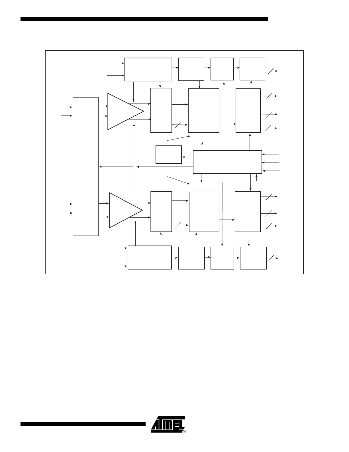
Figure 1. Simplified Block Diagram
AT84AD004
VINI
VINIB
VINQ
VINQB
INPUT
MUX
CLKI
DDRB
Gain control I
Calibration
Gain/offset
ISA I
Gain control Q
Calibration
Gain/offset
ISA Q & FiSDA
+
S/H
-
Input switch
+
S/H
-
Clock Buffer
ADC
ADC
8bit
8bit
Q
Divider
2 to16
DoirI
I
8
BIT
DoirQ
8
DMUX
DMUX
DRDA
I
1:2
or
1:1
I
DMUX control
3-wire Serial Interface
3WSI
DMUX control
1:2
or
1:1
Q
LVDS
Clock
Buffer
LVDS
Buffer
I
LVDS
buffer
Q
16
16
16
16
2
CLKIO
DOAI
DOAIN
DOBI
DOBIN
2
DOIRI
DOIRIN
Data
Clock
Ldn
Mode
2
DOIRQ
DOIRQN
DOAQ
DOAQN
DOBQ
DOBQN
CLKQ
DDRB
Clock Buffer
Divider
2 to 16
DRDA
Q
LVDS
Clock
Buffer
2
CLKQO
5390A–BDC–06/04
3
Page 4
Typical Applications
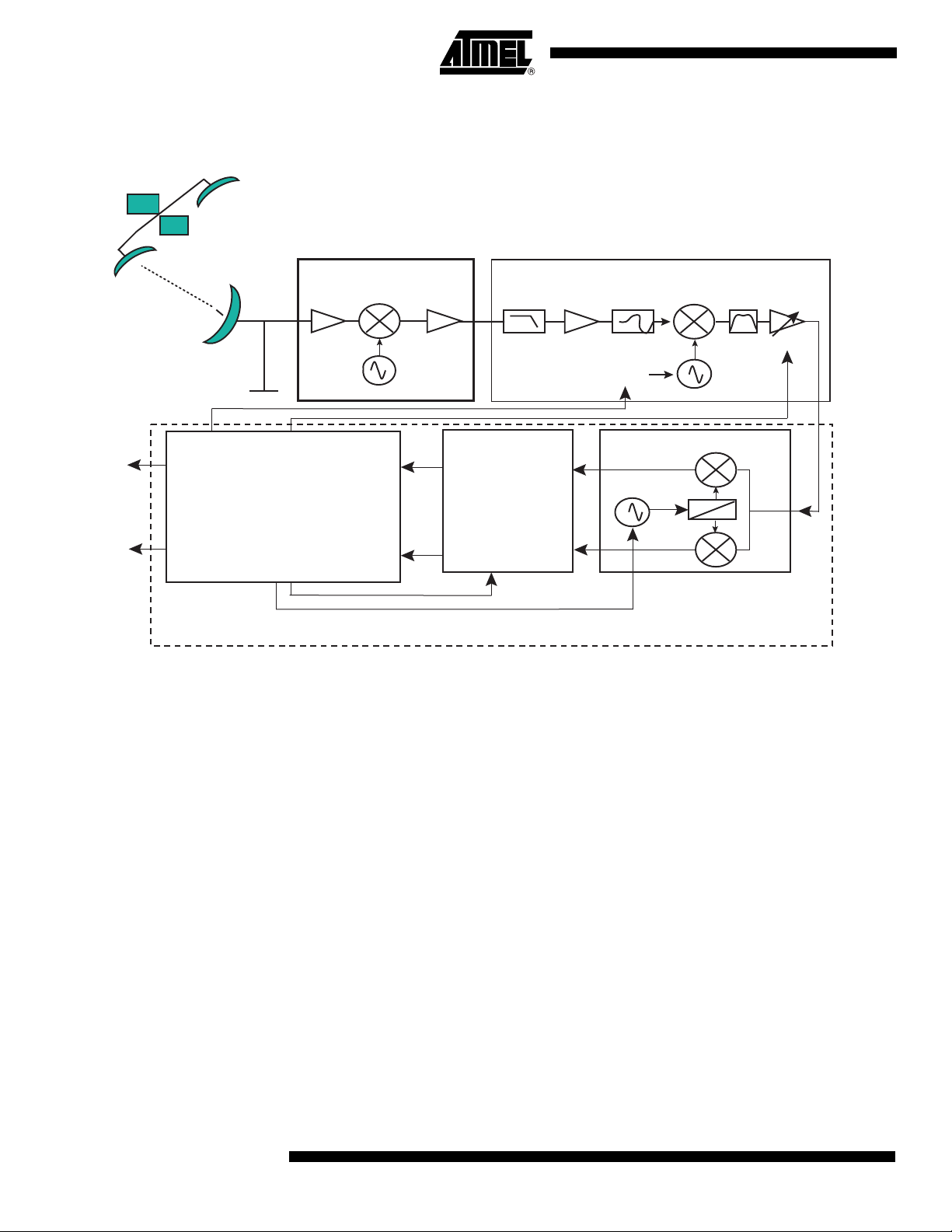
Figure 2. Satellite Receiver Application
Satellite
Dish
I
Control Functions:
Clock and Carrier
Recovery...
Q
Low Noise Converter
(Connected to the Dish)
Bandpass
Amplifier
11..12 GHz
Local Oscillator
Bandpass
Amplifier
I
Q
Demodulation
1..2 GHz
Low Pass
Filter
AT84AD004
Clock
Satellite Tuner
Tunable
Band Filter
Synthesizer
1.5 … 2.5 GHz
I
Local Oscillator
Q
Q
Band Filter
0
90
Quadrature
IF
AGC
4
AT84AD004
5390A–BDC–06/04
Page 5
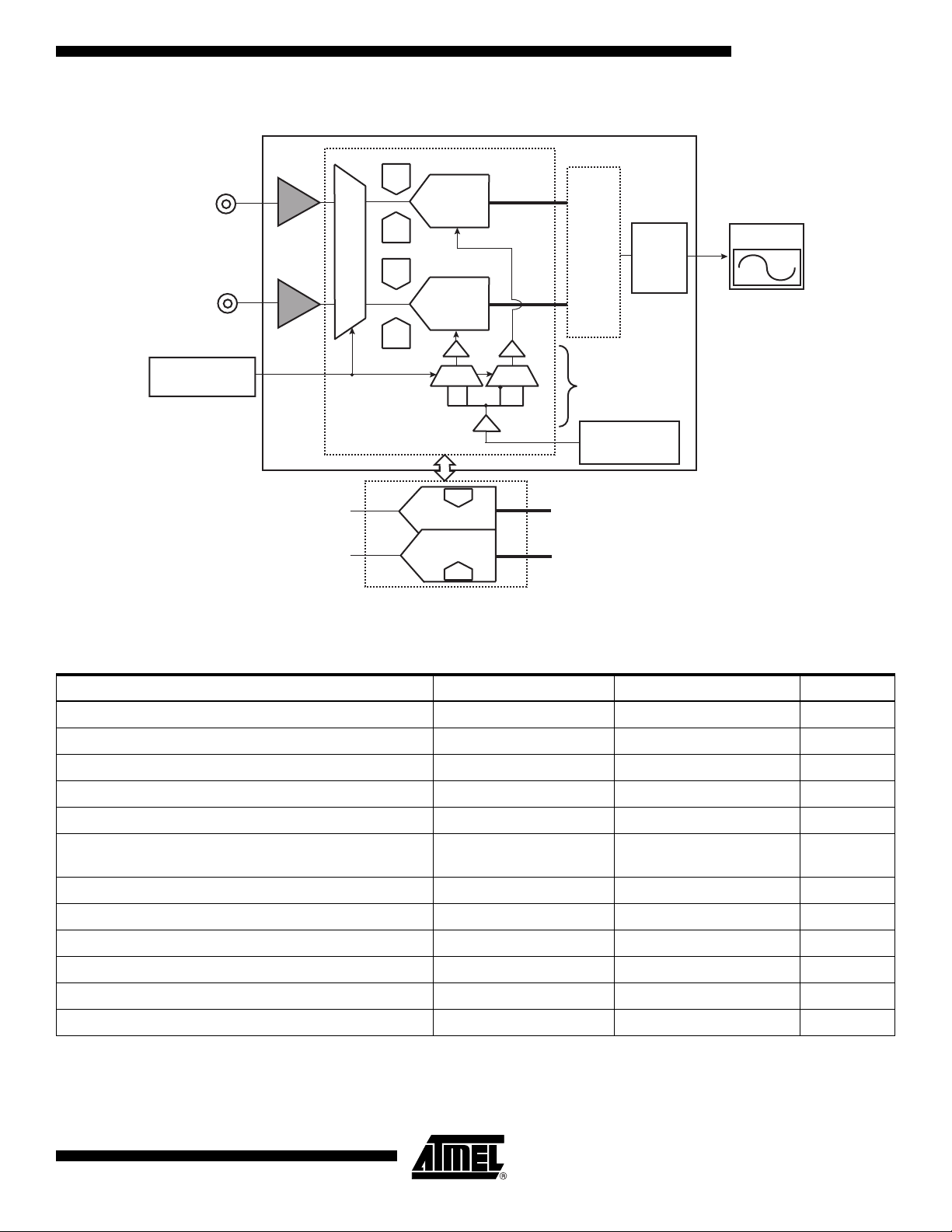
Figure 3. Dual Channel Digital Oscilloscope Application
DAC
Channel B
A
Channel A
A
Gain
ADC B
DAC
Offset
DAC
Offset
Analog Switch
DAC
Gain
ADC A
FISO
RAM
AT84AD004
Display
µP
Channel Mode
Selection
Clock
Selection
Timing
Circuit
DACs
Smart Dual
ADC
DACs
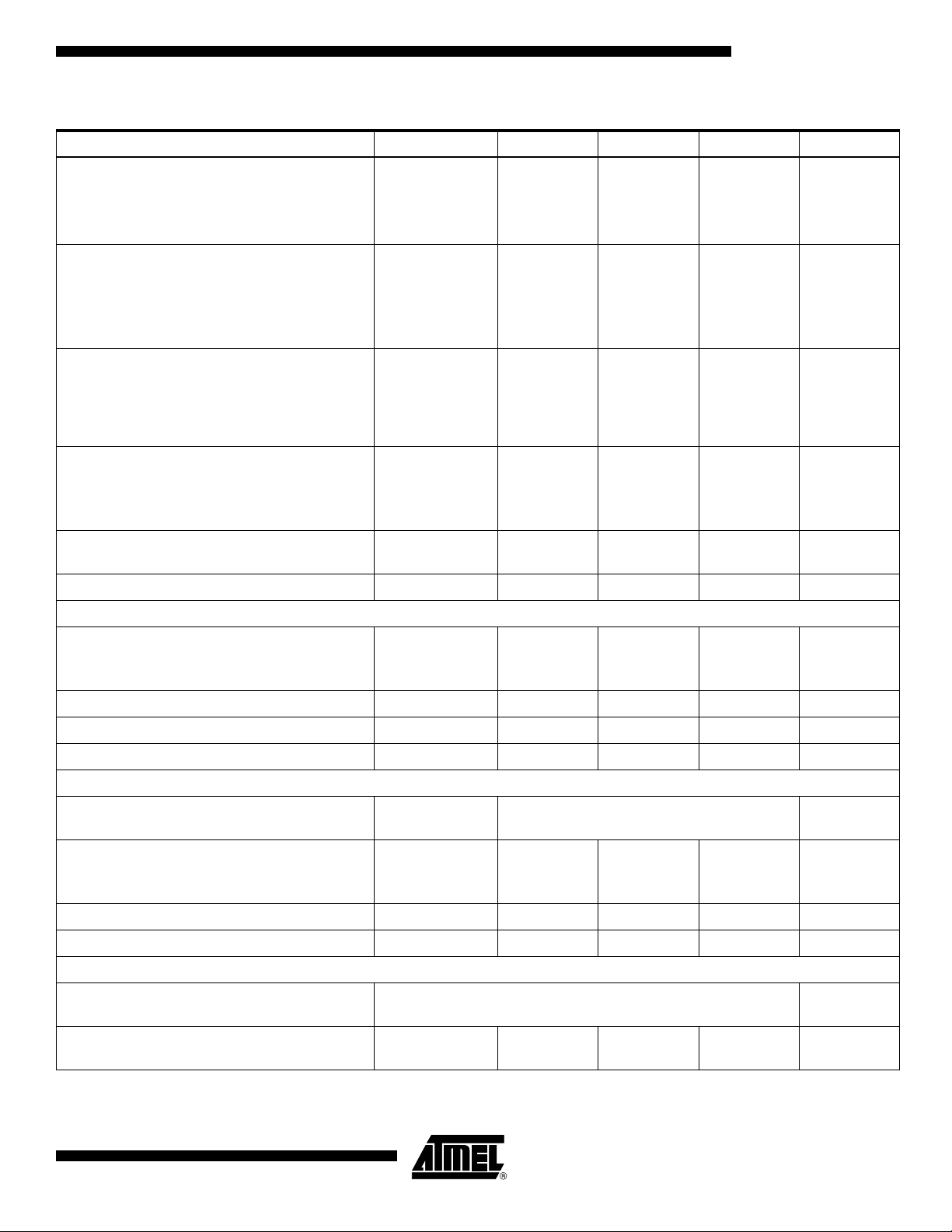
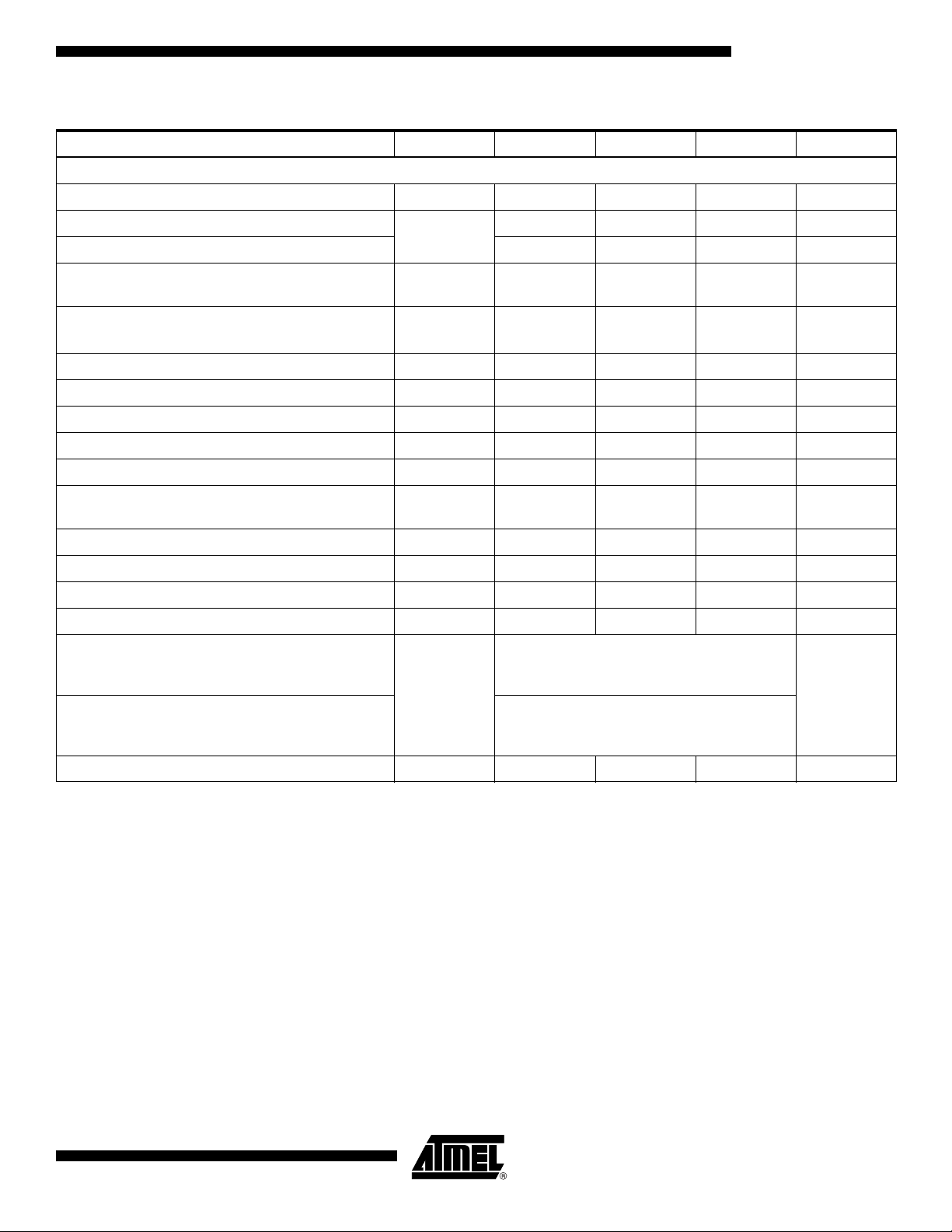
Absolute Maximum Ratings
Parameter Symbol Value Unit
Analog positive supply voltage V
Digital positive supply voltage V
Output supply voltage V
Maximum difference between V
Minimum V
CCO
Analog input voltage
CCA
and V
CCD
V
CCA
V
or V
V
INI
V
or V
INQ
Digital input voltage V
Clock input voltage V
Maximum difference between V
CLK
and V
CLKB
CLK
V
or VC
CLK
Maximum junction temperature T
Storage temperature T
Lead temperature (soldering 10s) T
CCA
CCD
CCO
to V
CCO
D
- V
J
stg
leads
CCD
INIB
INQB
LKB
CLKB
3.6 V
3.6 V
3.6 V
± 0.8 V
1.6 V
1/-1 V
-0.3 to V
-0.3 to V
+ 0.3 V
CCD
+ 0.3 V
CCD
-2 to 2 V
125 °C
-65 to 150 °C
300 °C
Note: Absolute maximum ratings are limiting values (referenced to GND = 0V), to be applied individually, while other parameters are
within specified operating conditions. Long exposure to maximum ratings may affect device reliability.
5
5390A–BDC–06/04
Page 6
Recommended Conditions of Use
Parameter Symbol Comments Recommended Value Unit
Analog supply voltage V
Digital supply voltage V
Output supply voltage V
Differential analog input voltage (full-scale)
CCA
CCD
CCO
V
-V
INQ
-V
IniB
or
INQB
INi
V
Differential clock input level Vinclk 600 mVpp
3.3 V
3.3 V
2.25 V
500 mVpp
Internal Settling Adjustment (ISA) with a 3-wire
serial interface for channel I and channel Q
Operating temperature range T
ISA -50 ps
Ambient
Commercial grade
Industrial grade
0 < T
-40 < T
< 70
A
< 85
A
Electrical Operating Characteristics
Unless otherwise specified:
•V
•V
• LVDS digital outputs (100Ω)
•T
• Full temperature range: 0°C < T
Table 1. Electrical Operating Characteristics in Nominal Conditions
Parameter Symbol Min Typ Max Unit
= 3.3V; V
CCA
- V
INI
INB
(typical) = 25°C
A
or V
CCD
INQ
(industrial grade)
= 3.3V; V
- V
INQB
= 2.25V
CCO
= 500 mVpp full-scale differential input
< 70°C (commercial grade) or -40°C < TA < 85°C
A
°C
Resolution 8Bits
Power Requirements
Positive supply voltage
- Analog
- Digital
Output digital (LVDS) and serial interface
V
V
V
CCA
CCD
CCO
3.15
3.15
2.0
3.3
3.3
2.25
3.45
3.45
2.5
V
V
V
Supply current (typical conditions)
- Analog
- Digital
- Output
I
CCA
I
CCD
I
CCO
150
230
100
180
275
120
mA
mA
mA
Supply current (1:2 DMUX mode)
- Analog
- Digital
- Output
6
AT84AD004
I
CCA
I
CCD
I
CCO
150
260
175
180
310
210
mA
mA
5390A–BDC–06/04
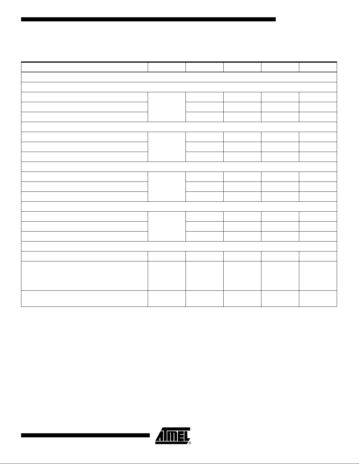
Page 7
AT84AD004
Table 1. Electrical Operating Characteristics in Nominal Conditions (Continued)
Parameter Symbol Min Typ Max Unit
Supply current (2 input clocks, 1:2 DMUX mode)
- Analog
- Digital
- Output
Supply current
(1 channel only, 1:1 DMUX mode)
- Analog
- Digital
- Output
Supply current
(1 channel only, 1:2 DMUX mode)
- Analog
- Digital
- Output
I
CCA
I
CCD
I
CCO
I
CCA
I
CCD
I
CCO
I
CCA
I
CCD
I
CCO
150
290
180
80
160
55
80
170
90
180
350
215
95
190
65
95
205
110
mA
mA
mA
mA
mA
mA
mA
Supply current (full standby mode)
- Analog
- Digital
- Output
Nominal dissipation
(1 clock, 1:1 DMUX mode, 2 channels)
I
CCA
I
CCD
I
CCO
P
12
24
3
D
1.4 1.7 W
17
34
5
mA
mA
mA
Nominal dissipation (full standby mode) stbpd 120 mW
Analog Inputs
- V
or
- V
IniB
mV
450 500 550
INQB
IN
2pF
mV
V
INi
Full-scale differential analog input voltage
V
INQ
Analog input capacitance I and Q C
Full power input bandwidth (-3 dB) FPBW 1.0 GHz
Gain flatness (-0.5 dB) 400 MHz
Clock Input
Logic compatibility for clock inputs and DDRB
Reset (pins 124,125,126,127,128,129)
PECL/ECL/LVDS
PECL/LVDS clock inputs voltages
(V
CLKI/IN
or V
CLKQ/QN
)
- V
V
IL
IH
600 mV
Differential logical level
Clock input power level -9 0 6 dBm
Clock input capacitance 2 pF
Digital Outputs
Logic compatibility for digital outputs
(depending on the value of V
CCO
)
Differential output voltage swings
(assuming V
5390A–BDC–06/04
= 2.25V)
CCO
V
OD
LV DS
220 270 350 mV
7
Page 8
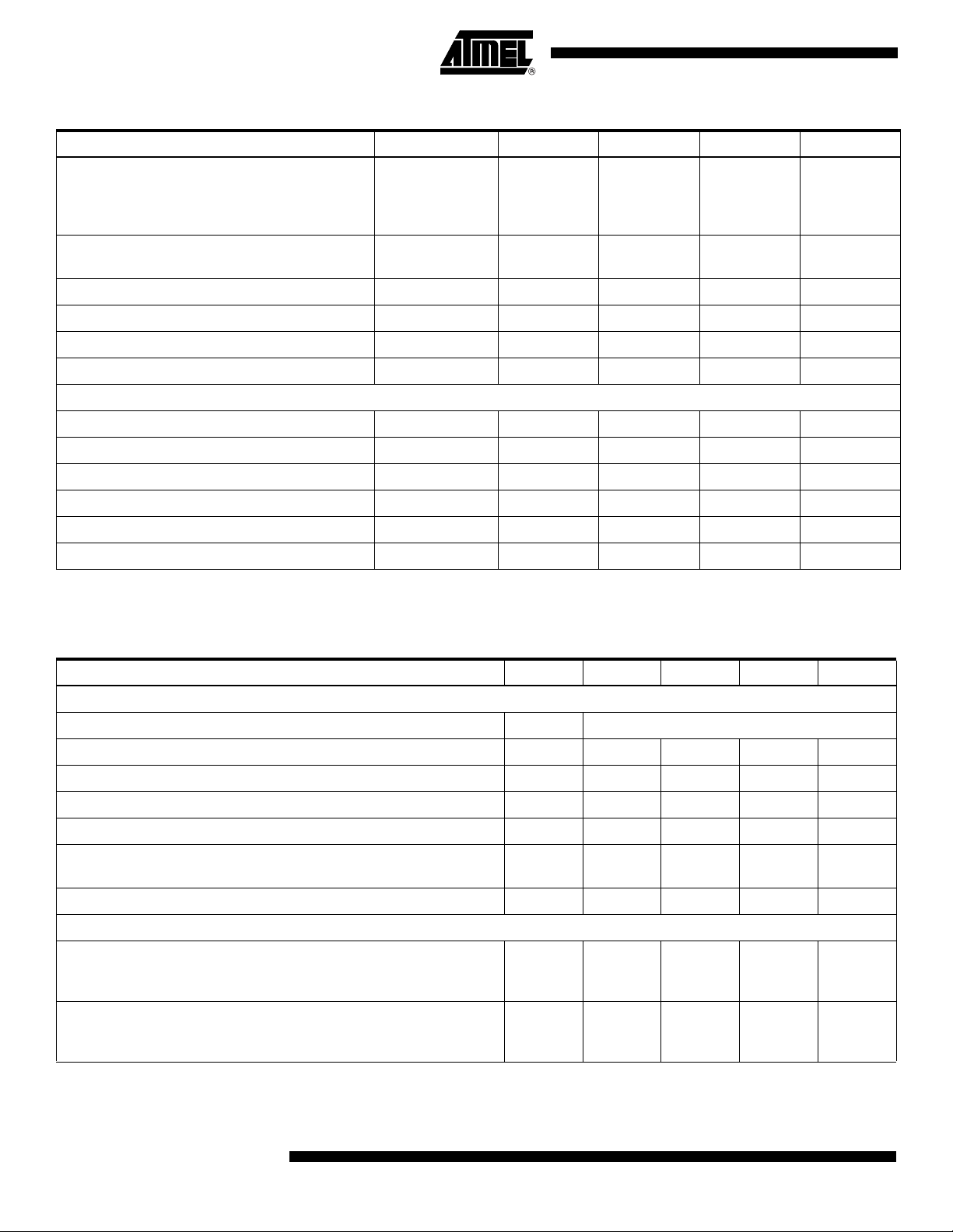
Table 1. Electrical Operating Characteristics in Nominal Conditions (Continued)
Parameter Symbol Min Typ Max Unit
Output levels (assuming V
100Ω differentially terminated
Logic 0 voltage
Logic 1 voltage
Output offset voltage (assuming V
100Ω differentially terminated
Output impedance R
Output current (shorted output) 12 mA
Output current (grounded output) 30 mA
Output level drift with temperature 1.3 mV/°C
Digital Input (Serial Interface)
Maximum clock frequency (input clk) Fclk 50 MHz
Input logical level 0 (clk, mode, data, ldn) -0.4 0 0.4 V
= 2.25V)
CCO
= 2.25V)
CCO
V
OL
V
OH
V
OS
O
1.0
1.25
1125 1250 1325 mV
1.1
1.35
1.2
1.45
50 W
V
V
Input logical level 1 (clk, mode, data, ldn) V
- 0.4 V
CCO
- 0.4 V
CCO
+ 0.4 V
CCO
Output logical level 0 (cal) -0.4 0 0.4 V
Output logical level 1 (cal) V
- 0.4 V
CCO
CCO
V
+ 0.4 V
CCO
Maximum output load (cal) 15 pF
Note: The gain setting is 0 dB, one clock input, no standby mode [full power mode], 1:1 DMUX, calibration off.
Table 2. Electrical Operating Characteristics
Parameter Symbol Min Typ Max Unit
DC Accuracy
No missing code Guaranteed over specified temperature range
Differential non-linearity DNL 0.25 0.6 LSB
Integral non-linearity INL 0.5 1 LSB
Gain error (single channel I or Q) with calibration -0.5 0 0.5 LSB
Input offset matching (single channel I or Q) with calibration -0.5 0 0.5 LSB
Gain error drift against temperature
Gain error drift against V
CCA
0.062
0.064
Mean output offset code with calibration 127 127.5 128 LSB
Transient Performance
Bit Error Rate
Fs = 1 Gsps
BER 10
-15
10
-12
Fin = 250 MHz
LSB/°C
LSB/mV
Error/
sample
ADC settling time channel I or Q
(between 10% - 90% of output response)
-V
Ini
= 500 mVpp
iniB
V
TS 170 ps
Note: The gain setting is 0 dB, two clock inputs, no standby mode [full power mode], 1:2 DMUX, calibration on.
8
AT84AD004
5390A–BDC–06/04
Page 9
AT84AD004
Table 3. AC Performances
Parameter Symbol Min Typ Max Unit
AC Performance
Signal-to-noise Ratio
Fs = 500 Msps Fin = 20 MHz
Fs = 500 Msps Fin = 250 MHz 41 43 dBc
Fs = 500 Msps Fin = 500 MHz 42 dBc
Effective Number of Bits
Fs = 500 Msps Fin = 20 MHz
Fs = 500 Msps Fin = 250 MHz 6.7 7.0 Bits
Fs = 500 Msps Fin = 500 MHz 6.8 Bits
Total Harmonic Distortion (First 9 Harmonics)
Fs = 500 Msps Fin = 20 MHz
Fs = 500 Msps Fin = 250 MHz 47 53 dBc
Fs = 500 Msps Fin = 500 MHz 51 dBc
Spurious Free Dynamic Range
Fs = 500 Msps Fin = 20 MHz
Fs = 500 Msps Fin = 250 MHz 49 55 dBc
Fs = 500 Msps Fin = 500 MHz 54 dBc
Two-tone Inter-modulation Distortion (Single Channel)
= 249 MHz , F
F
IN1
Phase matching using auto-calibration and FiSDA
in interlace mode (channel I and Q)
Fin = 250 MHz
Fs = 500 Msps
= 251 MHz at Fs = 500 Msps IMD -54 dBc
IN2
SNR
ENOB
|THD|
|SFDR|
dϕ -0.7 0 0.7 °
42 44 dBc
77.2 Bits
48 54 dBc
50 56 dBc
Crosstalk channel I versus channel Q
Fin = 250 MHz, Fs = 500 Msps
Notes: 1. Differential input [-1 dBFS analog input level], gain setting is 0 dB, two input clock signals, no standby mode,
1:1 DMUX, ISA = -50 ps.
2. Measured on the AT84AD004TD-EB Evaluation Board.
5390A–BDC–06/04
(2)
Cr -55 dB
9
Page 10
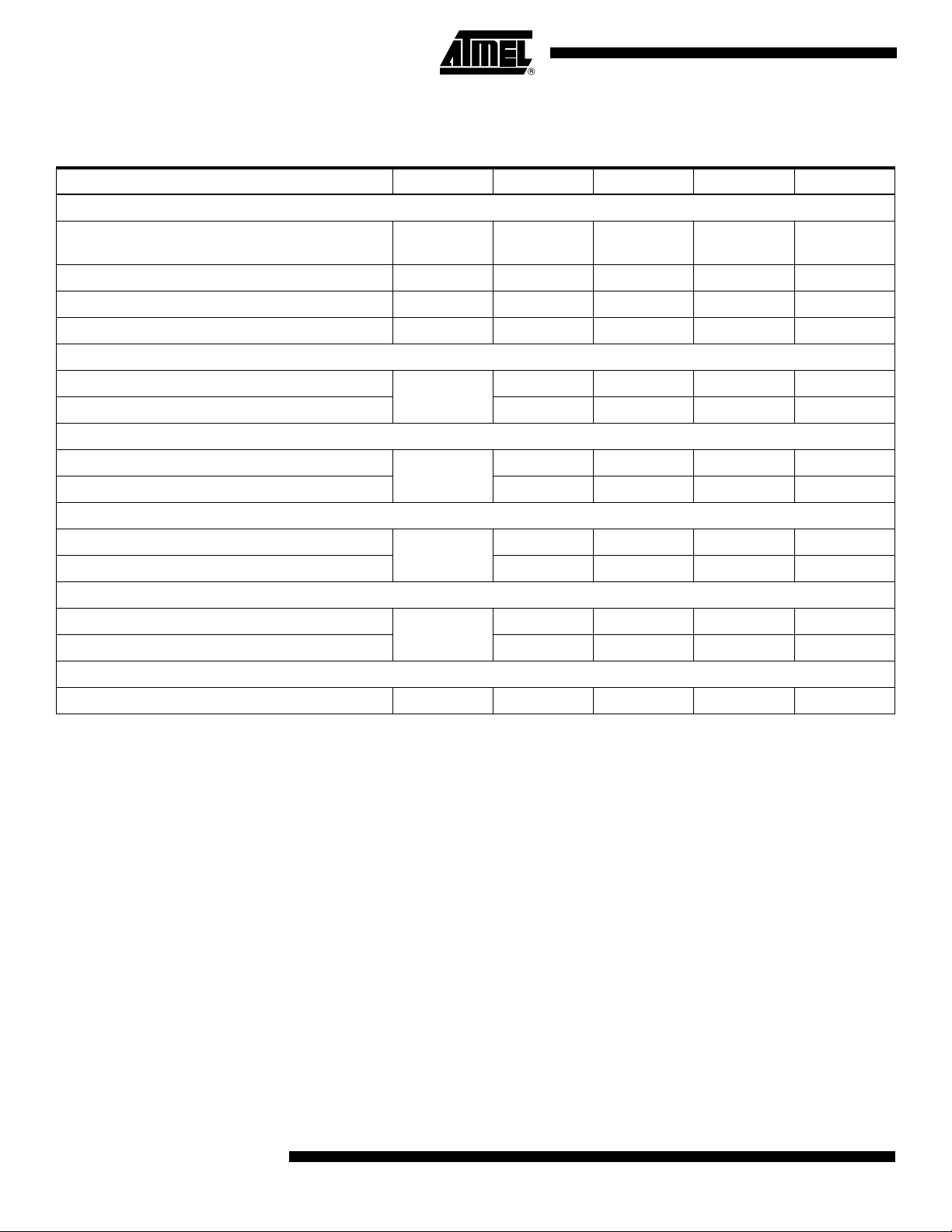
Table 4. AC Performances in Interlace Mode
Parameter Symbol Min Typ Max Unit
Interlace Mode
Maximum equivalent clock frequency Fint = 2 x Fs
Where Fs = external clock frequency
Minimum clock frequency F
F
int
int
1Gsps
20 Msps
Differential non-linearity in interlace mode intDNL 0.25 LSB
Integral non-linearity in interlace mode intINL 0.5 LSB
Signal-to-noise Ratio in Interlace Mode
Fint = 1 Gsps Fin = 20 MHz
42 dBc
iSNR
Fint = 1 Gsps Fin = 250 MHz 40 dBc
Effective Number of Bits in Interlace Mode
Fint = 1 Gsps Fin = 20 MHz
7.1 Bits
iENOB
Fint = 1 Gsps Fin = 250 MHz 6.8 Bits
Total Harmonic Distortion in Interlace Mode
Fint = 1 Gsps Fin = 20 MHz
52 dBc
|iTHD|
Fint = 1 Gsps Fin = 250 MHz 49 dBc
Spurious Free Dynamic Range in Interlace Mode
Fint = 1 Gsps Fin = 20 MHz
|iSFDR|
54 dBc
Fint = 1 Gsps Fin = 250 MHz 52 dBc
Two-tone Inter-modulation Distortion (Single Channel) in Interlace Mode
= 249 MHz , F
F
IN1
= 251 MHz at F
IN2
= 1 Gsps iIMD -54 dBc
int
Note: One analog input on both cores, clock I samples the analog input on the rising and falling edges. The calibration
phase is necessary. The gain setting is 0 dB, one input clock I, no standby mode, 1:1 DMUX, FiSDA adjustment.
10
AT84AD004
5390A–BDC–06/04
Page 11
AT84AD004
Table 5. Switching Performances
Parameter Symbol Min Typ Max Unit
Switching Performance and Characteristics - See “Timing Diagrams” on page 12.
Maximum operating clock frequency F
Minimum clock frequency (no transparent mode)
Minimum clock frequency (with transparent mode) 1 Ksps
S
F
S
500 Msps
10 Msps
Minimum clock pulse width [high]
(No transparent mode)
Minimum clock pulse width [low]
(No transparent mode)
Aperture delay: nominal mode with ISA & FiSDA TA 1 ns
Aperture uncertainty Jitter 0.4 ps (rms)
Data output delay between input clock and data TDO 3.8 ns
Data Ready Output Delay TDR 3 ns
Data Ready Reset to Data Ready TRDR 2 ns
Data Output Delay with Data Ready TD2
Data Ready (CLKO) Delay Adjust (140 ps steps) Tdrda range -560 to 420 ps
Output skew 50 100 ps
Output rise/fall time for DATA (20% - 80%) TR/TF 300 350 500 ps
Output rise/fall time for DATA READY (20% - 80%) TR/TF 300 350 500 ps
Data pipeline delay (nominal mode)
Data pipeline delay (nominal mode) in S/H
transparent mode
DDRB recommended pulse width 1 ns
TC1 0.4 1 50 ns
TC2 0.4 1 50 ns
1/2 Fs
+Tdrda
3 (port B)
3.5 (port A, 1:1 DMUX mode)
TPD
4 (port A, 1:2 DMUX mode)
2.5 (port B)
3 (port A, 1:1 DMUX mode)
3.5 (port A, 1:2 DMUX mode)
Clock cycles
ps
5390A–BDC–06/04
11
Page 12
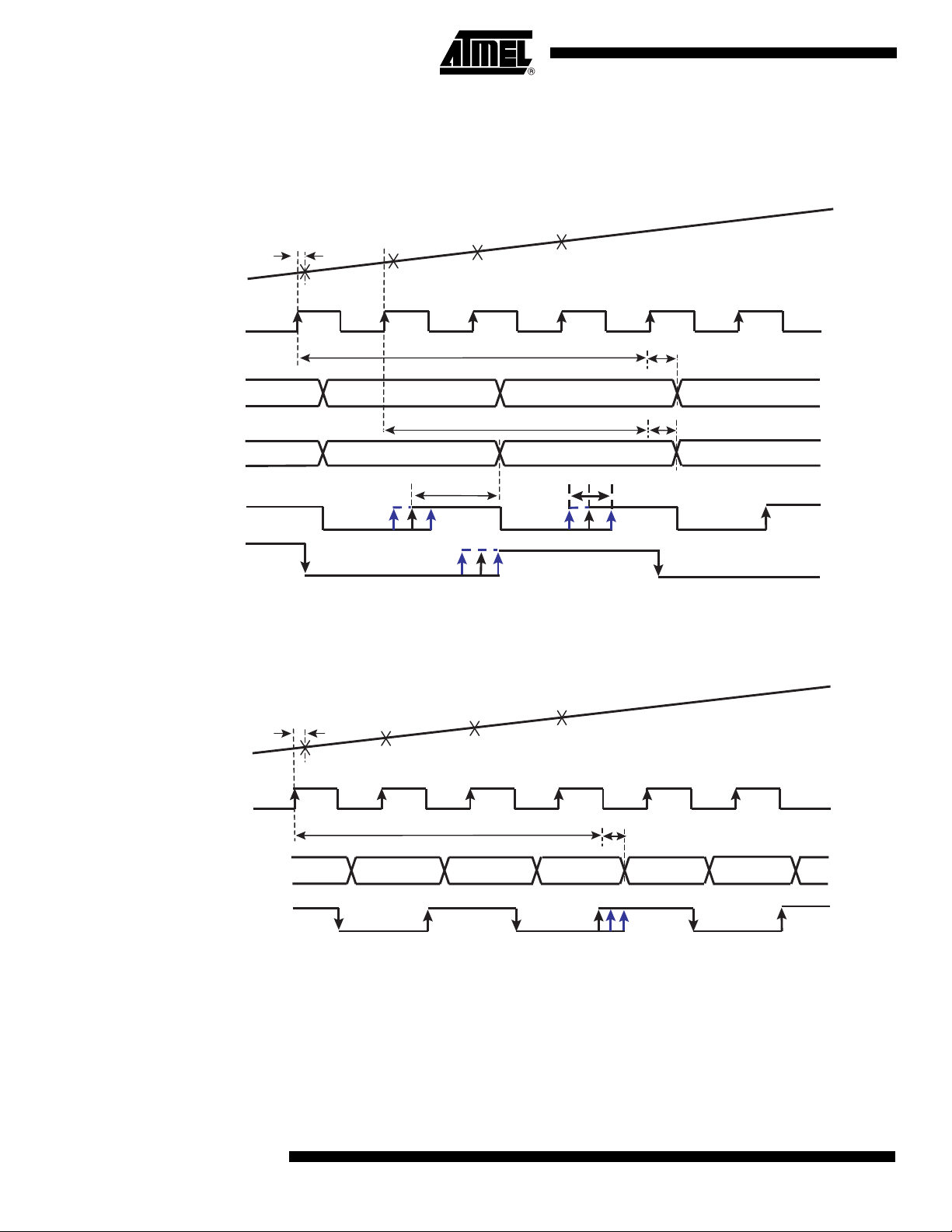
Timing Diagrams
Figure 4. Timing Diagram, ADC I or ADC Q, 1:2 DMUX Mode, Clock I for ADC I, Clock Q for ADC Q
Address: D7 D6 D5 D4 D3 D2 D1 D0
1 1 X X 1 X 0 0
TA
VIN
N + 1
N
N + 2
CLKI or CLKQ
Pipeline delay = 4 clock cycles
DOIA[0:7]
or DOQA[0:7]
DOIB[0:7]
or DOQB[0:7]
N - 4
Pipeline delay = 3 clock cycles
N - 3 N - 1 N +1
TD2
CLKOI or CLKOQ
(= CLKI/2)
CLKOI or CLKOQ
(= CLKI/4)
Figure 5. 1:1 DMUX Mode, Clock I = ADC I, Clock Q = ADC Q
Address: D7 D6 D5 D4 D3 D2 D1 D0
1 1 X X 0 X 0 0
N + 3
N - 2
Programmable delay
TDO
N
TDO
12
TA
VIN
N
N + 1
CLKI or CLKQ
Pipeline delay = 3.5 clock cycles
DOIA[0:7]
or DOQA[0:7]
N - 3
CLKOI or CLKOQ
DOIB[0:7] and DOQB[0:7] are high impedance
AT84AD004
N + 2
N - 2
N + 3
N - 1
TDO
N
N + 1
5390A–BDC–06/04
Page 13
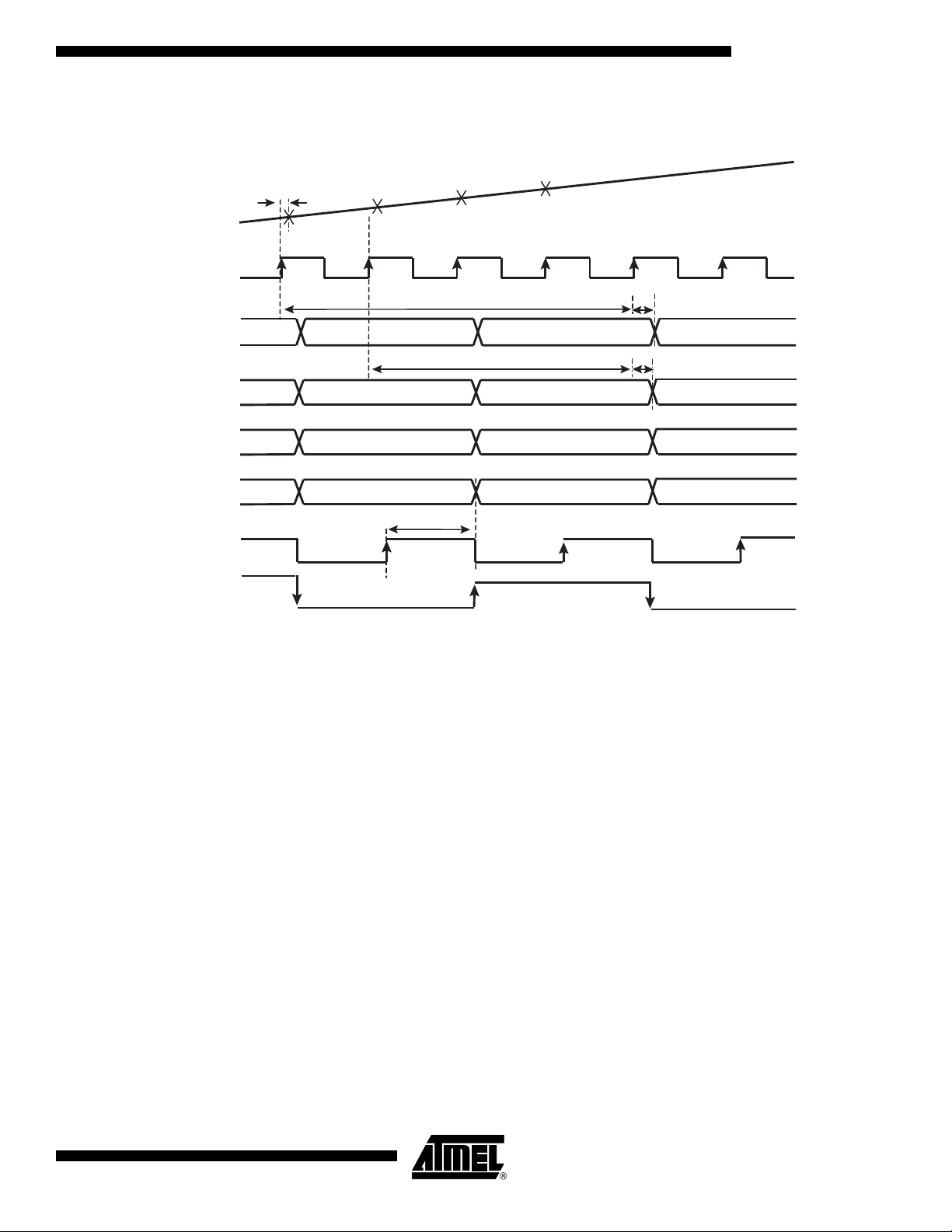
Figure 6. 1:2 DMUX Mode, Clock I = ADC I, Clock I = ADC Q
Address: D7 D6 D5 D4 D3 D2 D1 D0
1 0 X X 1 X 0 0
AT84AD004
TA
VIN
N
CLKI
DOIA[0:7]
DOIB[0:7]
DOQA[0:7]
DOQB[0:7]
CLKOI
(= CLKI/2)
CLKOI
(= CLKI/4)
CLKOQ is high impedance
N + 1
Pipeline delay = 4 clock cycles
NI - 4
Pipeline delay = 3 clock cycles
NI - 3 NI - 1 NI +1
NQ - 4 NQ - 2 NQ
NQ - 3 NQ - 1 NQ +1
N + 2
TD2
N + 3
NI - 2
TDO
NI
TDO
5390A–BDC–06/04
13
Page 14
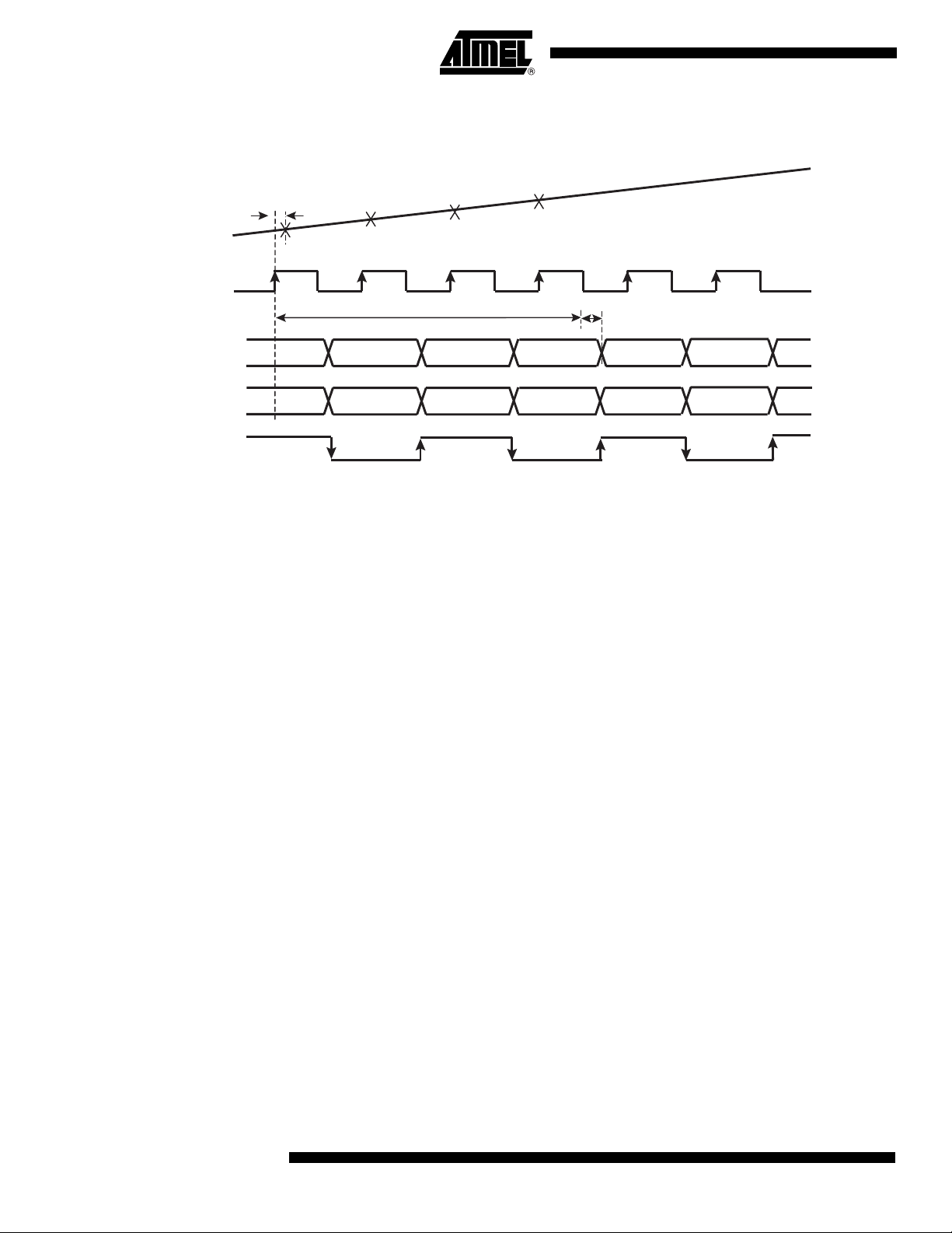
Figure 7. 1:1 DMUX Mode, Clock I = ADC I, Clock I = ADC Q
Address: D7 D6 D5 D4 D3 D2 D1 D0
1 0 X X 0 X 0 0
TA
VIN
N
N + 1
CLKI
Pipeline delay = 3.5 clock cycles
DOIA[0:7]
DOQA[0:7]
N - 3
N - 3
CLKOI
DOIB[0:7] and DOQB[0:7] are high impedance
CLKOQ is high impedance
N + 2
N - 2
N - 2
N + 3
N - 1
N - 1
TDO
N
N
N + 1
N + 1
14
AT84AD004
5390A–BDC–06/04
Page 15
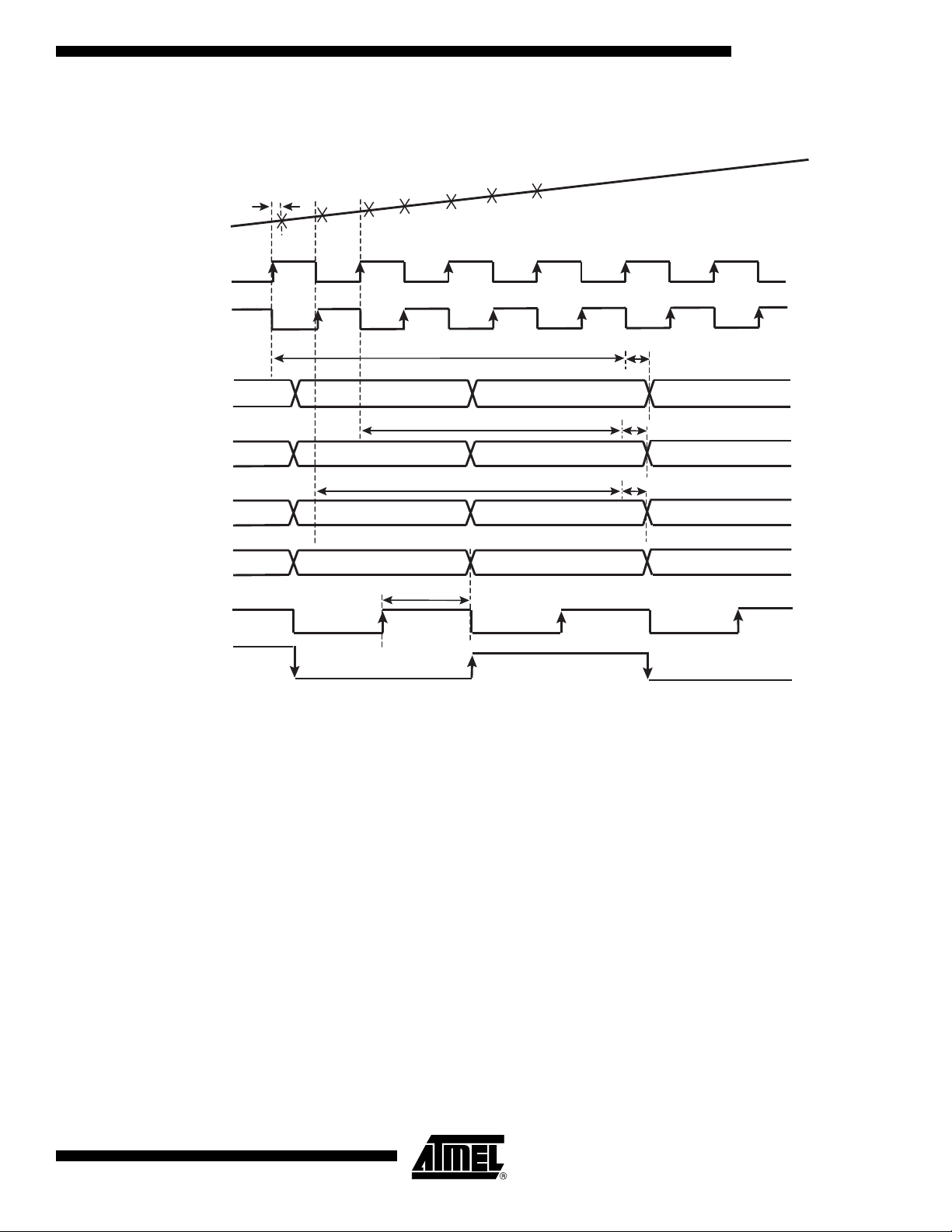
Figure 8. 1:2 DMUX Mode, Clock I = ADC I, Clock IN = ADC Q
Address: D7 D6 D5 D4 D3 D2 D1 D0
0 X X X 1 X 0 0
N + 4
N + 5
VIN
CLKI
CLKIN
TA
N + 2
N + 1
N
N + 3
AT84AD004
N + 6
DOQA[0:7]
DOQB[0:7]
DOIA[0:7]
DOIB[0:7]
CLKOI
(= CLKI/2)
CLKOI
(= CLKI/4)
CLKOQ is high impedance
Pipeline delay = 4 clock cycles
N - 8
Pipeline delay = 3 clock cycles
N - 6 N - 2 N + 2
Pipeline delay = 3.5 clock cycles
N - 7 N - 3 N + 1
N - 5 N - 1 N + 3
TD2
N - 4
TDO
N
TDO
TDO
5390A–BDC–06/04
15
Page 16
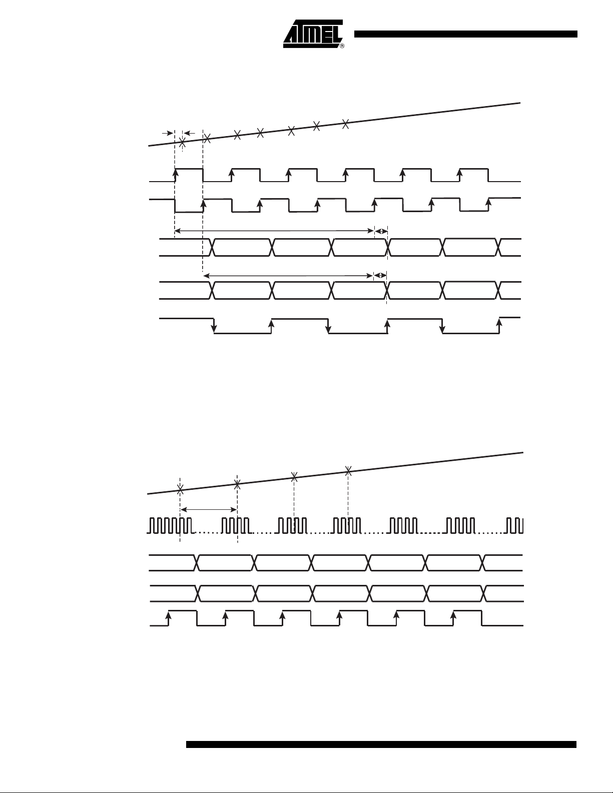
Figure 9. 1:1 DMUX Mode, Clock I = ADC I, Clock IN = ADC Q
Address: D7 D6 D5 D4 D3 D2 D1 D0
0 X X X 0 X 0 0
N + 4
N + 5
VIN
TA
N + 2
N + 1
N
N + 3
CLKI
CLKIN
N + 6
Pipeline delay = 3.5 clock cycles
DOQA[0:7]
DOIA[0:7]
N - 6
Pipeline delay = 3 clock cycles
N - 5
N - 4
N - 3
CLKOI
(= CLKI/2)
DOIB[0:7] and DOQB[0:7] are high impedance
CLKOQ is high impedance
Figure 10. 1:1 DMUX Mode, Decimation Mode Test (1:16 Factor)
Address: D7 D6 D5 D4 D3 D2 D1 D0
1 0 X X 0 X 0 0
N + 16
VIN
N - 16
16 clock cycles
N
N - 2
N - 1
N + 32
TDO
TDO
N
N + 1
N + 2
N + 3
CLKI
DOIA[0:7]
DOQA[0:7]
N - 16
N - 16
N
N
CLKOI
DOIB[0:7] and DOQB[0:7] are high impedance
CLKOQ is high impedance
Notes: 1. Frequency(CLKOI) = Frequency(Data) = Frequency(CLKI)/16.
16
AT84AD004
N + 16 N + 32 N + 48
N + 16 N + 32 N + 48
5390A–BDC–06/04
Page 17
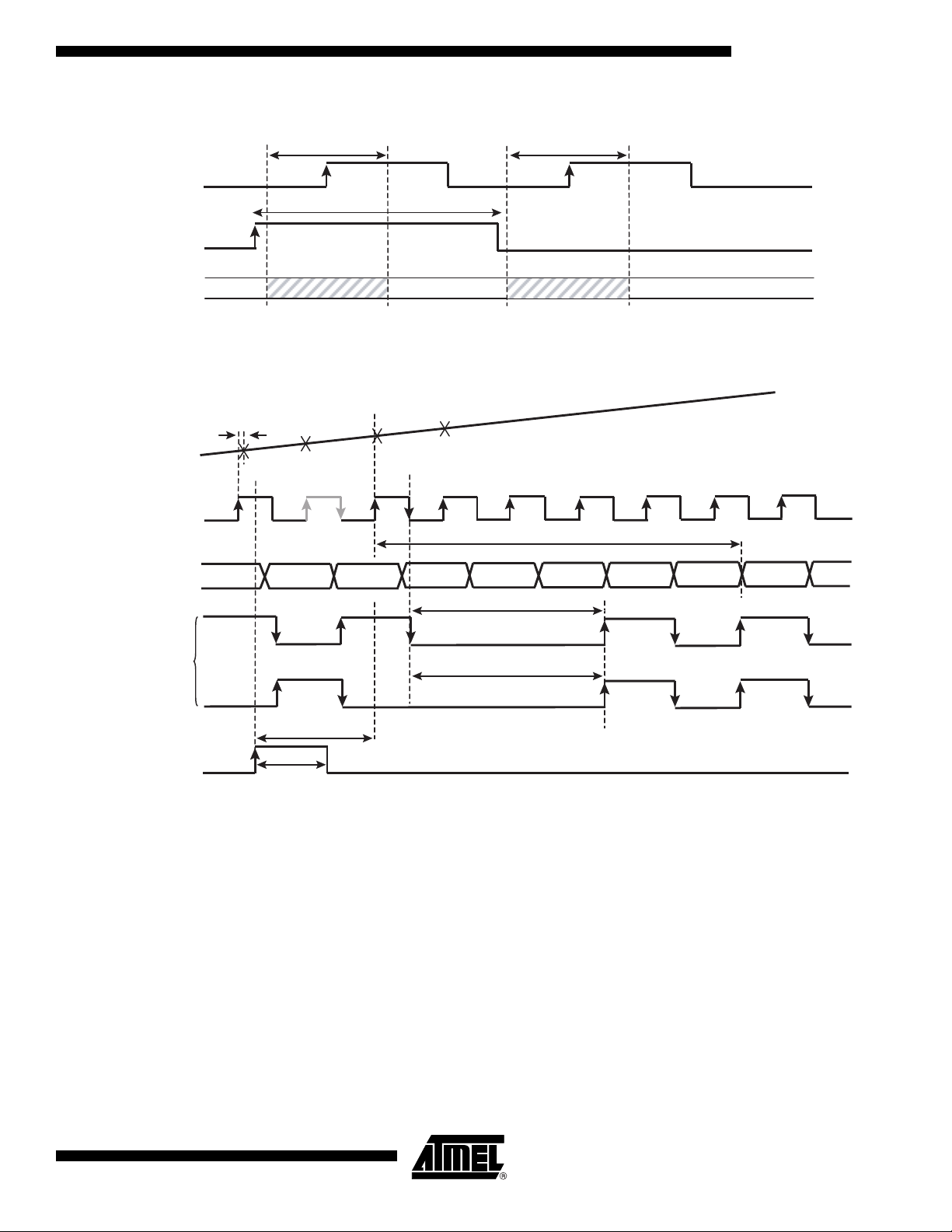
Figure 11. Data Ready Reset
AT84AD004
500 ps
CLKI or
CLKQ
1 ns min
DDRB
Figure 12. Data Ready Reset 1:1 DMUX Mode
TA
VIN
Clock in
Reset
CLKI or
CLKQ
DOIA[0:7] or
DOQA[0:7]
N
ALLOWED
N + 1
500 ps
FORBIDDENFORBIDDEN
ALLOWED
Pipeline Delay + TDO
N
TDR
CLKOI or
CLKOQ
2 ns
TDR
DDRB
1 ns min
Note: The Data Ready Reset is taken into account only 2 ns after it is asserted. The output clock first completes its cycle (if the reset
occurs when it is high, it goes low only when its half cycle is complete; if the reset occurs when it is low, it remains low) and then
only, remains in reset state (frozen to a low level in 1:1 DMUX mode). The next falling edge of the input clock after reset makes
the output clock return to normal mode (after TDR).
5390A–BDC–06/04
17
Page 18
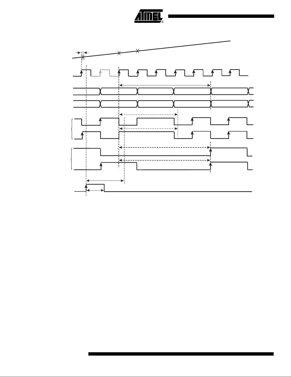
Figure 13. Data Ready Reset 1:2 DMUX Mode
TA
VIN
CLKI or
CLKQ
DOIA[0:7] or
DOQA[0:7]
Clock in
Reset
N
N + 1
Pipeline Delay + TDO
N
DOIB[0:7] or
DOQB[0:7]
CLKOI or CLKOQ
(= CLKI/2)
CLKOI or CLKOQ
(= CLKI/4)
DDRB
Notes: 1. In 1:2 DMUX, Fs/2 mode:
The Data Ready Reset is taken into account only 2 ns after it is asserted. The output clock first completes its cycle (if the
reset occurs when it is low, it goes high only when its half cycle is complete; if the reset occurs when it is high, it remains
high) and then only, remains in reset state (frozen to a high level in 1:2 DMUX Fs/2 mode). The next rising edge of the input
clock after reset makes the output clock return to normal mode (after TDR).
2. In 1:2 DMUX, Fs/4 mode:
The Data Ready Reset is taken into account only 2 ns after it is asserted. The output clock first completes its cycle (if the
reset occurs when it is high, it goes low only when its half cycle is complete; if the reset occurs when it is low, it remains low)
and then only, remains in reset state (frozen to a low level in 1:2 DMUX Fs/4 mode). The next rising edge of the input clock
after reset makes the output clock return to normal mode (after TDR).
N + 1
TDR
TDR
TDR + 2 cycles
TDR + 2 cycles
2 ns
1 ns min
18
AT84AD004
5390A–BDC–06/04
Page 19

Functions Description
Table 6. Description of Functions
Name Function
V
CCA
V
CCD
V
CCO
GNDA Analog ground
GNDD Digital ground
GNDO Output ground
V
, V
INI
INIB
V
, V
INQ
INQB
CLKOI, CLKOIN, CLKOQ,
CLKOQN
CLKI, CLKIN, CLKQ, CLKQN Differential clock inputs I and Q
DDRB, DDRBN
Mode
Clk
Data Input data for 3-wire bus
Ldn
<D0AI0:DOAI7>
<D0AI0N:DOAI7N>
<D0BI0:DOBI7>
<D0BI0N:DOBI7N>
<D0AQ0:DOAQ7>
<D0AQ0N:DOAQ7N>
<D0BQ0:DOBQ7>
<D0BQ0N:DOBQ7N>
Positive analog power supply
Positive digital power supply
Positive output power supply
Differential analog inputs I
Differential analog inputs Q
Differential output data ready I
and Q
Synchronous data ready reset
I and Q
Bit selection for 3-wire bus or
nominal setting
Input clock for 3-wire bus
interface
Beginning and end of register
line for 3-wire bus interface
Differential output data port
channel I
Differential output data port
channel Q
VINI
VINIB
VINQ
VINQB
CLKI
CLKIB
CLKQ
CLKQB
VCCA = 3.3V
GNDA
VCCD = 3.3V VCCO = 2.25V
AT84AD004
mode dataclk ldn
GNDO
GNDD
AT84AD004
D0AI0 DOAI7
D0AI0N DOAI7N
32
D0BI0
DOBI7
D0BI0N
DOBI7N
D0AQ0 DOAQ7
32
D0AQ0 DOAQ7
DOBQ0
DOQBQ7
DOBQ0N
DOQBQ7N
4
DOIRI, DOIRIN
DOIRQ, DOIRQN
4
CLOCKOI, CLOCKOIB
CLOCKOQ, CLOCKOQB
2
VtestI
VtestQ
Vdiode
DOIRI, DOIRIN DOIRQ,
DOIRQN
VtestQ
VtestI
Cal
Vdiode
5390A–BDC–06/04
Differential output IN range
data I and Q
Test voltage output for ADC Q
(to be left open)
Test voltage output for ADC I
(to be left open)
Output bit status internal
calibration
Test diode voltage for Tj
measurement
19
Page 20

Digital Output Coding (Nominal Settings)
Table 7. Digital Output Coding (Nominal Setting)
Differential
Analog Input
Voltag e Level
Digital Output
I or Q (Binary Coding)
Out-of-range Bit
> 250 mV > Positive full-scale + 1/2 LSB 1 1 1 1 1 1 1 1 1
250 mV
248 mV
1 mV
-1 mV
-248 mV
-250 mV
Positive full-scale + 1/2 LSB
Positive full-scale - 1/2 LSB
Bipolar zero + 1/2 LSB
Bipolar zero - 1/2 LSB
Negative full-scale + 1/2 LSB
Negative full-scale - 1/2 LSB
1 1 1 1 1 1 1 1
1 1 1 1 1 1 1 0
1 0 0 0 0 0 0 0
0 1 1 1 1 1 1 1
0 0 0 0 0 0 0 1
0 0 0 0 0 0 0 0
< -250 mV < Negative full-scale - 1/2 LSB 0 0 0 0 0 0 0 0 1
Pin Description
Table 8. AT84AD004 LQFP 144 Pin Description
Symbol Pin number Function
GNDA, GNDD, GNDO
V
CCA
V
CCD
V
CCO
V
INI
V
INIB
V
INQ
10, 12, 22, 24, 36, 38, 40, 42, 44, 46, 51,
54, 59, 61, 63, 65, 67, 69, 85, 87, 97, 99,
109, 111, 130, 142, 144
41, 43, 45, 60, 62, 64 Analog positive supply: 3.3V typical
9, 21, 37, 39, 66, 68, 88, 100, 112, 123,
141
11, 23, 86, 98, 110, 143
57, 58
55, 56
47, 48
Ground pins. To be connected to external
ground plane
3.3V digital supply
2.25V output and 3-wire serial interface
supply
In-phase (+) analog input signal of the
sample & hold differential preamplifier
channel I
Inverted phase (-) of analog input signal
)
(V
INI
In-phase (+) analog input signal of the
sample & hold differential preamplifier
channel Q
0
0
0
0
0
0
V
INQB
49, 50
Inverted phase (-) of analog input signal
(V
)
INQ
CLKI 124 In-phase (+) clock input signal
CLKIN 125
Inverted phase (-) clock input signal
(CLKI)
CLKQ 129 In-phase (+) clock input signal
20
AT84AD004
5390A–BDC–06/04
Page 21

AT84AD004
Table 8. AT84AD004 LQFP 144 Pin Description (Continued)
Symbol Pin number Function
CLKQN 128
DDRB 126 Synchronous data ready reset I and Q
DDRBN 127 Inverted phase (-) of input signal (DDRB)
Inverted phase (-) clock input signal
(CLKQ)
DOAI0, DOAI1, DOAI2, DOAI3, DOAI4,
DOAI5, DOAI6, DOAI7
DOAI0N, DOAI1N, DOAI2N, DOAI3N,
DOAI4N, DOAI5N, DOAI6N, DOAI7N,
DOBI0, DOBI1, DOBI2, DOBI3, DOBI4,
DOBI5, DOBI6, DOBI7
DOBI0N, DOBI1N, DOBI2N, DOBI3N,
DOBI4N, DOBI5N, DOBI6N, DOBI7N
DOAQ0, DOAQ1, DOAQ2, DOAQ3,
DOAQ4, DOAQ5, DOAQ6, DOAQ7
DOAQ0N, DOAQ1N, DOAQ2N, DOAQ3N,
DOAQ4N, DOAQ5N, DOAQ6N, DOAQ7N
DOBQ0, DOBQ1, DOBQ2, DOBQ3,
DOBQ4, DOBQ5, DOBQ6, DOBQ7
DOBQ0N, DOBQ1N, DOBQ2N,
DOBQ3N, DOBQ4N, DOBQ5N,
DOBQ6N, DOBQ7N
117, 113, 105, 101, 93, 89, 81, 77
118, 114, 106, 102, 94, 90, 82, 78
119, 115, 107, 103, 95, 91, 83, 79
120, 116, 108, 104, 96, 92, 84, 80
136, 140, 4, 8, 16, 20, 28, 32
135, 139, 3, 7, 15, 19, 27, 31
134, 138, 2, 6, 14, 18, 26, 30
133, 137, 1 ,5, 13, 17, 25, 29
In-phase (+) digital outputs first phase
demultiplexer (channel I) DOAI0 is the
LSB. D0AI7 is the MSB
Inverted phase (-) digital outputs first
phase demultiplexer (channel I) DOAI0N
is the LSB. D0AI7N is the MSB
In-phase (+) digital outputs second phase
demultiplexer (channel I) DOBI0 is the
LSB. D0BI7 is the MSB
Inverted phase (-) digital outputs second
phase demultiplexer (channel I) DOBI0N
is the LSB. D0BI7N is the MSB
In-phase (+) digital outputs first phase
demultiplexer (channel Q) DOAI0 is the
LSB. D0AQ7 is the MSB
Inverted phase (-) digital outputs first
phase demultiplexer (channel Q) DOAI0N
is the LSB. D0AQ7N is the MSB
In-phase (+) digital outputs second phase
demultiplexer (channel Q) DOBQ0 is the
LSB. D0BQ7 is the MSB
Inverted phase (-) digital outputs second
phase demultiplexer (channel Q)
DOBQ0N is the LSB. D0BQ7N is the MSB
In-phase (+) out-of-range bit input
DOIRI 75
DOIRIN 76 Inverted phase of output signal DOIRI
DOIRQ 34
DOIRQN 33 Inverted phase of output signal DOIRQ
MODE 74
CLK 73 Input clock for 3-wire bus interface
DATA 72 Input data for 3-wire bus
LND 71
CLKOI 121 Output clock in-phase (+) channel I
5390A–BDC–06/04
(I phase) combined demultiplexer
out-of-range is high on the leading edge of
code 0 and code 256
In-phase (+) out-of-range bit input
(Q phase) combined demultiplexer
out-of-range is high on the leading edge of
code 0 and code 256
Bit selection for 3-wire bus interface or
nominal setting
Beginning and end of register line for
3- wire bus interface
21
Page 22

Table 8. AT84AD004 LQFP 144 Pin Description (Continued)
Symbol Pin number Function
CLKOIN 122 Inverted phase (-) output clock channel I
CLKOQ 132
CLKOQN 131 Inverted phase (-) output clock channel Q
VtestQ, VtestI 52, 53 Pins for internal test (to be left open)
Cal 70 Calibration output bit status
Vdiode 35
Figure 14. AT84AD004 Pinout (Top View)
Output clock in-phase (+) channel Q,
1/2 input clock frequency
Positive node of diode used for die
junction temperature measurements
LQFP 144
20 by 20 by 1.4 mm
Atmel - Dual 8-bit
22
AT84AD004
5390A–BDC–06/04
Page 23

Typical Characterization Results
Nominal conditions (unless otherwise specified):
•V
•V
• LVDS digital outputs (100Ω)
• TA (typical) = 25°C
• Full temperature range: 0
= 3.3V; V
CCA
- V
INI
INB
or -40
°C < TA < 85° C (industrial grade)
or V
= 3.3V; V
CCD
to V
INQ
= 2.25V
CCO
= 500 mVpp full-scale differential input
INQB
°C < TA < 70°C (commercial grade)
AT84AD004
Typical Full Power Input Bandwidth
• Fs = 500 Msps
• Pclock = 0 dBm
•Pin = -1 dBFS
• Gain flatness (±5 dB) from DC to > 400 MHz
• Full power input bandwidth at -3 dB > 1 GHz
Figure 15. Full Power Input Bandwidth
0
-1
-2
-3
dBFS
-4
-5
-6
-7
250 500 750 1000 1250 1500
Fin (MHz)
-3 dB BandwidthGain Flatness
5390A–BDC–06/04
23
Page 24

Typical Crosstalk Figure 16. Crosstalk (Fs = 500 Msps)
80
70
60
50
40
dBc
30
20
10
0
0 100 200 300 400 500 600 700 800 900 1000
Note: Measured on the AT84AD004TD-EB Evaluation Board.
Fin (MHz)
Typical DC, INL and DNL Patterns
1:2 DMUX mode, Fs/4 DR type
Figure 17. Typical INL (Fs = 50 Msps, Fin = 1 MHz, Saturated Input)
0,6
0,4
0,2
0
INL (Lsb )
-0,2
-0,4
-0,6
1 16 31 46 61 76 91 106 121 136 151 166 181 196 211 226 241 256
Codes
24
AT84AD004
5390A–BDC–06/04
Page 25

AT84AD004
Figure 18. Typical DNL (Fs = 50 Msps, Fin = 1 MHz, Saturated Input)
0.3
0.2
0.1
0
DNL (Lsb)
-0.1
-0.2
-0.3
1 16 31 46 61 76 91 106 121 136 151 166 181 196 211 226 241 256
Codes
Typical Dynamic Performances Versus Sampling Frequency
Figure 19. ENOB Versus Sampling Frequency in Nyquist Conditions (Fin = Fs/2)
7.6
7.4
7.2
7.0
6.8
ENOB (Bit)
6.6
6.4
6.2
6.0
50 100 150 200 250 300 350 400 450 500 550
Fs (Msps)
Figure 20. SFDR Versus Sampling Frequency in Nyquist Conditions (Fin = Fs/2)
-56
5390A–BDC–06/04
-59
-62
SFDR ( dBc)
-65
-68
50 100 150 200 250 300 350 400 450 500 550
Fs (Msps)
25
Page 26

Figure 21. THD Versus Sampling Frequency in Nyquist Conditions (Fin = Fs/2)
-48
-50
-52
-54
THD (dB c)
-56
-58
-60
50 100 150 200 250 300 350 400 450 500 550
Fs (Msps)
Figure 22. SNR Versus Sampling Frequency in Nyquist Conditions (Fin = Fs/2)
45
44
Typical Dynamic Performances Versus Input Frequency
43
SNR (d Bc)
42
41
40
50 100 150 200 250 300 350 400 450 500 550
Fs (Msps
Figure 23. ENOB Versus Input Frequency (Fs = 500 Msps)
7.6
7.4
7.2
7.0
6.8
ENOB (Bit)
6.6
6.4
6.2
0 100 200 300 400 500
Fin (MHz)
Channel I Channel Q
26
AT84AD004
5390A–BDC–06/04
Page 27

Figure 24. SFDR Versus Input Frequency (Fs = 500 Msps)
-46
-48
-50
-52
-54
-56
SFDR (dBc)
-58
-60
-62
-64
0 100 200 300 400 500
Fin (MHz)
Channel I Channel Q
Figure 25. THD Versus Input Frequency (Fs = 500 Msps)
-48
-49
-50
-51
-52
-53
THD (dBc)
-54
-55
-56
-57
-58
0 100 200 300 400 500
Fin (MHz)
AT84AD004
5390A–BDC–06/04
Channel I Channel Q
Figure 26. SNR Versus Input Frequency (Fs = 500 Msps)
45
44
43
SNR (dBc)
42
41
40
0 100 200 300 400 500
Fin (MHz)
Channel I Channel Q
27
Page 28

Typical Signal Spectrum Figure 27. Fs = 500 Msps and Fin = 20 MHz (1:2 DMUX, Fs/4 DR Type
FiSDA = -35 ps, ISA = -50 ps)
20
0
-20
-40
dBc
-60
-80
-100
-120
Figure 28. Fs = 500 Msps and Fin = 250 MHz (1:2 DMUX, Fs/4 DR Type
FiSDA = -35 ps, ISA = -50 ps)
20
0
Fundamental: H1
SFDR = -60 dBc
H2
0 16 31 47 63 78 94 109 125 141 156 172 188 203 219 234
H4
H3
Fs (Msps)
Fundamental : H1
-20
-40
dBc
-60
-80
-100
-120
H3
0 16 31 47 63 78 94 109 125 141 156 172 188 203 219 234
SFDR = -58 dBc
H2
Fs (Msps)
28
AT84AD004
5390A–BDC–06/04
Page 29

AT84AD004
Figure 29. Fs = 500 Msps and Fin = 500 MHz (1:2 DMUX, Fs/4 DR Type
FiSDA = -35 ps, ISA = -50 ps)
20
Fundamental: H1
0
-20
H2
-40
dBc
-60
-80
-100
-120
0 16 31 47 63 78 94 109 125 141 156 172 188 203 219 234
SFDR = -57 dBc
H3
Fs (Msps)
Note: The spectra are given with respect to the output clock frequency observed by the acquisi-
tion system (Figures 27 to 29).
Figure 30. Fs = 500 Msps and Fin = 250 MHz (Interleaving Mode Fint = 1 Gsps
1:1 DMUX, FiSDA = -35 ps, ISA = -50 ps)
20
Fundamental: H1
0
-20
SFDR = -53 dBc
dBc
-40
-60
5390A–BDC–06/04
-80
-100
-120
0 62 125 187 249 311 374 436 498
Fs (Msps)
Fs
29
Page 30

Typical Performance Sensitivity Versus Power Supplies and Temperature
Figure 31. ENOB Versus V
Fs/4 DR Type, ISA = -50 ps)
7.6
7.4
7.2
ENOB ( Bit)
7.0
6.8
6.6
3.1 3.15 3.2 3.25 3.3 3.35 3.4 3.45 3.5
(Fs = 500 Msps, Fin = 250 MHz, 1:2 DMUX,
CCA
Vcca (V)
Channel I Channel Q
Figure 32. SFDR Versus V
Fs/4 DR Type, ISA = -50 ps)
-48
-50
-52
-54
-56
SFDR (dBc)
-58
-60
-62
3.1 3.15 3.2 3.25 3.3 3.35 3.4 3.45 3.5
(Fs = 500 Msps, Fin = 250 MHz, 1:2 DMUX,
CCA
Vcca (V)
Channel I Channel Q
30
AT84AD004
5390A–BDC–06/04
Page 31

AT84AD004
Figure 33. THD Versus V
Fs/4 DR Type, ISA = -50 ps)
-48
-49
-50
-51
-52
-53
THD (dBc)
-54
-55
-56
-57
-58
3.1 3.15 3.2 3.25 3.3 3.35 3.4 3.45 3.5
Figure 34. SNR Versus V
Fs/4 DR Type, ISA = -50 ps)
46.0
45.0
(Fs = 500 Msps, Fin = 250 MHz, 1:2 DMUX,
CCA
Vcca (V)
Channel I Channel Q
(Fs = 500 Msps, Fin = 250 MHz, 1:2 DMUX,
CCA
44.0
SNR (dBc)
43.0
42.0
41.0
3.1 3.15 3.2 3.25 3.3 3.35 3.4 3.45 3.5
Vcca (V)
Channel I Channel Q
5390A–BDC–06/04
31
Page 32

Figure 35. ENOB Versus Junction Temperature (Fs = 500 Msps, Fin = 250 MHz,
1:2 DMUX, Fs/4 DR Type, ISA = -50 ps)
7.4
7.2
7.0
6.8
6.6
ENOB (Bit)
6.4
6.2
6.0
-50 -25 0 25 50 75 100
Tj (˚C)
500 Msps 20 MHz
500 Msps 250 MHz
500 Msps 500 MHz
Figure 36. SFDR Versus Junction Temperature (Fs = 500 Msps, Fin = 250 MHz,
1:2 DMUX, Fs/4 DR Type, ISA = -50 ps)
-46
-48
-50
-52
-54
500 Msps 500 MHz
500 Msps 250 MHz
500 Msps 20 MHz
-56
SFDR (dBc)
-58
-60
-62
-50 -25 0 25 50 75 100
Tj (˚C)
32
AT84AD004
5390A–BDC–06/04
Page 33

AT84AD004
p
Figure 37. THD Versus Junction Temperature (Fs = 500 Msps, Fin = 250 MHz,
1:2 DMUX, Fs/4 DR Type, ISA = -50 ps)
-44
-46
-48
-50
-52
THD (dBc)
-54
-56
-58
-50 -25 0 25 50 75 100
Tj (˚C)
s 500 MHz
500 Ms
500 Msps 250 MHz
500 Msps 20 MHz
Figure 38. SNR Versus Junction Temperature (Fs = 500 Msps, Fin = 250 MHz,
1:2 DMUX, Fs/4 DR Type, ISA = -50 ps)
46
45
44
43
SNR (d Bc)
42
500 Msps 20 MHz
500 Msps 250 MHz
500 Msps 500 MHz
5390A–BDC–06/04
41
40
-50 -25 0 25 50 75 100
Tj (˚C)
33
Page 34

Test and Control Features
3-wire Serial Interface Control Setting
Table 9. 3-wire Serial Interface Control Settings
Mode Characteristics
Mode = 1 (2.25V) 3-wire serial bus interface activated
3-wire serial bus interface deactivated
Nominal setting:
Dual channel I and Q activated
One clock I
0 dB gain
DMUX mode 1:1
Mode = 0 (0V)
DRDA I & Q = 0 ps
ISA I & Q = 0 ps
FiSDA Q = 0 ps
Binary output
Decimation test mode OFF
Calibration setting OFF
Data Ready = Fs /2
34
AT84AD004
5390A–BDC–06/04
Page 35

AT84AD004
3-wire Serial Interface and Data Description
The 3-wire bus is activated with the control bit mode set to 1. The length of the word is
19 bits: 16 for the data and 3 for the address. The maximum clock frequency is
50 MHz.
Table 10. 3-wire Serial Interface Address Setting Description
Address Setting
Standby
Gray/binary mode
1:1 or 1:2 DMUX mode
000
001
010
011
100
Analog input MUX
Clock selection
Auto-calibration
Decimation test mode
Data Ready Delay Adjust
Analog gain adjustment
Data7 to Data0: gain channel I
Data15 to Data8: gain channel Q
Code 00000000: -1.5 dB
Code 10000000: 0 dB
Code 11111111: 1.5 dB
Steps: 0.011 dB
Offset compensation
Data7 to Data0: offset channel I
Data15 to Data8: offset channel Q
Data7 and Data15: sign bits
Code 11111111b: 31.75 LSB
Code 10000000b: 0 LSB
Code 00000000b: 0 LSB
Code 01111111b: -31.75 LSB
Steps: 0.25 LSB
Maximum correction: ±31.75 LSB
Gain compensation
Data6 to Data0: channel I/Q (Q is matched to I)
Code 11111111b: -0.315 dB
Code 10000000b: 0 dB
Code 0000000b: 0 dB
Code 0111111b: 0.315 dB
Steps: 0.005 dB
Data6: sign bit
Internal Settling Adjustment (ISA)
Data2 to Data0: channel I
Data5 to Data3: channel Q
Data15 to Data6: 1000010000
5390A–BDC–06/04
35
Page 36

Table 10. 3-wire Serial Interface Address Setting Description (Continued)
Address Setting
Testability
Data3 to Data0 = 0000
101
110
111
Mode S/H transparent OFF: Data4 = 0 ON: Data4 = 1
Data7 = 0
Data8 = 0
Built-In Test (BIT)
Data0 = 0 BIT Inactive Data0 = 1 BIT Active
Data1 = 0 Static BIT Data1 = 1 Dynamic BIT
If Data1 = 1, then Ports BI & BQ = Rising Ramp
Ports AI & AQ = Decreasing Ramp
If Data1 = 0, then Data2 to Data9 = Static Data for BIT
Ports BI & BQ = Data2 to Data9
Ports AI & AQ = NOT (Data2 to Data9)
Data Ready Delay Adjust (DRDA)
Data2 to Data0: clock I
Data5 to Data3: clock Q
Steps: 140 ps
000: -560 ps
100: 0 ps
111: 420 ps
Fine Sampling Delay Adjustment (FiSDA) on channel Q
Data10 to Data6: channel Q
Steps: 5 ps
Data4: sign bit
Code 11111: -75 ps
Code 10000: 0 ps
Code 00000: 0 ps
Code 01111: 75 ps
Notes: 1. The Internal Settling Adjustment could change independently of the two analog sampling times (TA channels I and Q) of the
sample/hold (with a fixed digital sampling time) with steps of ±50 ps:
Nominal mode will be given by Data2…Data0 = 100 or Data5…Data3 = 100.
Data5…Data3 = 000 or Data2…Data0 = 000: sampling time is -200 ps compared to nominal.
Data2…Data0 = 111 or Data5…Data3 = 111: sampling time is 150 ps compared to nominal.
We recommend setting the ISA to -50 ps to optimize the ADC’s dynamic performances.
2. The Fine Sampling Delay Adjustment enables you to change the sampling time (steps of ±5 ps) on channel Q more precisely, particularly in the interleaved mode.
3. The “S/H transparent” mode (address 101, Data4) enables bypassing of the ADC’s track/hold. This function optimizes the
ADC’s performances at very low input frequencies (Fin < 50 MHz).
4. In the Gray mode, when the input signal is overflow (that is, the differential analog input is greater than 250 mV), the output
data must be corrected using the output DOIR:
If DOIR = 1: Data7 unchanged
Data6 = 0, Data5 = 0, Data4 = 0, Data3 = 0, Data2 = 0, Data1 = 0, Data0 = 0.
In 1:2 DMUX mode, only one out-of-range bit is provided for both A and B ports.
36
AT84AD004
5390A–BDC–06/04
Page 37

Table 11. 3-wire Serial Interface Data Setting Description
AT84AD004
Setting for Address:
000 D15 D14 D13 D12 D11 D10 D9
Full standby mode XXXXXX 0 XXXXXXX11
Standby channel I
Standby channel Q
No standby mode XXXXXX 0 XXXXXXX00
Binary output mode XXXXXX 0 XXXXXX1XX
Gray output mode XXXXXX 0 XXXXXX0XX
DMUX 1:2 mode XXXXXX 0 XXXXX1XXX
DMUX 1:1 mode XXXXXX 0 XXXXX0XXX
Analog selection mode
→ ADC I
Input I
Input Q → ADC Q
Analog selection mode
Input I
→ ADC I
Input I → ADC Q
Analog selection mode
Input Q
Input Q → ADC Q
→ ADC I
(2)
(3)
XXXXXX 0 XXXXXXX01
XXXXXX 0 XXXXXXX10
XXXXXX 0 XXX11XXXX
XXXXXX 0 XXX10XXXX
XXXXXX 0 XXX0XXXXX
(1)
D8 D7 D6 D5 D4 D3 D2 D1 D0
Clock Selection mode
CLKI
→ ADC I
CLKQ → ADC Q
Clock selection mode
CLKI
→ ADC I
CLKI → ADC Q
Clock selection mode
CLKI
→ ADC I
CLKIN → ADC Q
Decimation OFF modeXXXXXX 0 0XXXXXXXX
Decimation ON mode XXXXXX 0 1XXXXXXXX
Keep last calibration
calculated value
No calibration phase
No calibration phase
No calibration value
Start a new calibration
phase
(4)
(5)
XXXXXX 0 X11XXXXXX
XXXXXX 0 X10XXXXXX
XXXXXX 0 X0XXXXXXX
XXXX0 1 0 XXXXXXXXX
XXXX0 0 0 XXXXXXXXX
XXXX1 1 0 XXXXXXXXX
5390A–BDC–06/04
37
Page 38

Table 11. 3-wire Serial Interface Data Setting Description (Continued)
Setting for Address:
000 D15 D14 D13 D12 D11 D10 D9
Control wait bit
calibration
In 1:2 DMUX
FDataReady
I & Q = Fs/2
In 1:2 DMUX
FDataReady
I & Q = Fs/4
Notes: 1. D9 must be set to “0”
(6)
2. Mode standby channel I: use analog input I Vini, Vinib and Clocki.
3. Mode standby channel Q: use analog input Q Vinq, Vinqb and Clockq.
4. Keep last calibration calculated value - no calibration phase: D11 = 0 and D10 = 1. No new calibration is required. The values taken into account for the gain and offset are either from the last calibration phase or are default values (reset values).
5. No calibration phase - no calibration value: D11 = 0 and D10 = 0. No new calibration phase is required. The gain and offset
compensation functions can be accessed externally by writing in the registers at address 010 for the offset compensation
and at address 011 for the gain compensation.
6. The control wait bit gives the possibility to change the internal setting for the auto-calibration phase:
For high clock rates (= 500 Msps) use a = b = 1.
For clock rates > 250 Msps and < 500 Msps use a = 1 and b = 0.
For clock rates > 125 Msps and < 250 Msps use a = 0 and b = 1.
For low clock rates < 125 Msps use a = 0 and b = 0.
X X a b X X 0 XXXXXXXXX
X 0 X X X X 0 XXXXXXXXX
X 1 X X X X 0 XXXXXXXXX
(1)
D8 D7 D6 D5 D4 D3 D2 D1 D0
3-wire Serial Interface Timing Description
The 3-wire serial interface is a synchronous write-only serial interface made of three
wires:
• sclk: serial clock input
• sldn: serial load enable input
• sdata: serial data input
The 3-wire serial interface gives write-only access to as many as 8 different internal reg-
isters of up to 16 bits each. The input format is always fixed with 3 bits of register
address followed by 16 bits of data. The data and address are entered with the Most
Significant Bit (MSB) first.
The write procedure is fully synchronous with the rising clock edge of “sclk” and
described in the write chronogram (Figure 39 on page 39).
• “sldn” and “sdata” are sampled on each rising clock edge of “sclk” (clock cycle).
• “sldn” must be set to 1 when no write procedure is performed.
• A minimum of one rising clock edge (clock cycle) with “sldn” at 1 is required for a
correct start of the write procedure.
• A write starts on the first clock cycle with “sldn” at 0. “sldn” must stay at 0 during the
complete write procedure.
• During the first 3 clock cycles with “sldn” at 0, 3 bits of the register address from
MSB (a[2]) to LSB (a[0]) are entered.
• During the next 16 clock cycles with “sldn” at 0, 16 bits of data from MSB (d[15]) to
LSB (d[0]) are entered.
• An additional clock cycle with “sldn” at 0 is required for parallel transfer of the serial
data d[15:0] into the addressed register with address a[2:0]. This yields 20 clock
cycles with “sldn” at 0 for a normal write procedure.
38
AT84AD004
5390A–BDC–06/04
Page 39

Figure 39. Write Chronogram
AT84AD004
• A minimum of one clock cycle with “sldn” returned at 1 is requested to close the
write procedure and make the interface ready for a new write procedure. Any clock
cycle where “sldn” is at 1 before the write procedure is completed interrupts this
procedure and no further data transfer to the internal registers is performed.
• Additional clock cycles with “sldn” at 0 after the parallel data transfer to the register
(done at the 20th consecutive clock cycle with “sldn” at 0) do not affect the write
procedure and are ignored.
It is possible to have only one clock cycle with “sldn” at 1 between two following write
procedures.
• 16 bits of data must always be entered even if the internal addressed register has
less than 16 bits. Unused bits (usually MSBs) are ignored. Bit signification and bit
positions for the internal registers are detailed in Table 10 on page 35.
To reset the registers, the Pin mode can be used as a reset pin for chip initialization,
even when the 3-wire serial interface is used.
Mode
sclk
sldn
sdata
Internal register
value
Reset setting
Reset
12 345 1314151617181920
a[2] a[1]
a[0] d[15]
d[8]
d[7]
d[6]
d[5]
d[4]
d[3]
d[2]
d[1]
d[0]
New d
Write procedure
Figure 40. Timing Definition
Mode
sclk
sldn
Twlmode
Tdmode
Tssldn
Thsldn
Tsclk
Twsclk
Tdmode
5390A–BDC–06/04
sdata
Tssdata
Thsdata
39
Page 40

Table 12. Timing Description
Name Parameter
Tsclk Sclk period 20 ns
Twsclk High or low time of sclk 5 ns
Tssldn Setup time of sldn before rising edge of sclk 4 ns
Thsldn Hold time of sldn after rising edge of sclk 2 ns
Tssdata Setup time of sdata before rising edge of sclk 4 ns
Thsdata Hold time of sdata after rising edge of sclk 2 ns
Twlmode Minimum low pulse width of mode 5 ns
Tdmode
Minimum delay between an edge of mode and the
rising edge of sclk
Min Typ Max
10 ns
Value
Unit
Calibration Description The AT84AD004 offers the possibility of reducing offset and gain matching between the
two ADC cores. An internal digital calibration may start right after the 3-wire serial inter
face has been loaded (using data D12 of the 3-wire serial interface with address 000).
The beginning of calibration disables the two ADCs and a standard data acquisition is
performed. The output bit CAL goes to a high level during the entire calibration phase.
When this bit returns to a low level, the two ADCs are calibrated with offset and gain and
can be used again for a standard data acquisition.
If only one channel is selected (I or Q) the offset calibration duration is divided by two
and no gain calibration between the two channels is necessary.
-
Figure 41. Internal Timing Calibration
3-wire Serial Interface
LDN
CAL
Tcal
The Tcal duration is a multiple of the clock frequency ClockI (master clock). Even if a
dual clock scheme is used during calibration, ClockQ will not be used.
The control wait bits (D13 and D14) give the possibility of changing the calibration’s setting depending on the clock’s frequency:
• For high clock rates (= 500 Msps) use a = b = 1, Tcal = 10112 clock I periods.
• For clock rates > 250 Msps and < 500 Msps use a = 1, b = 0, Tcal = 6016 clock I
periods.
• For clock rates > 125 Msps and < 250 Msps use a = 0, b = 1 ,Tcal = 3968 clock I
periods.
• For low clock rates (< 125 Msps) use a = 0, b = 0 , Tcal = 2944 clock I periods.
40
AT84AD004
5390A–BDC–06/04
Page 41

The calibration phase is necessary when using the AT84AD004 in interlace mode,
where one analog input is sampled at both ADC cores on the common input clock’s ris
ing and falling edges. This operation is equivalent to converting the analog signal at
twice the clock frequency
Table 13. Matching Between Channels
AT84AD004
-
Parameter
Gain error (single channel I or Q) without calibration 0 LSB
Gain error (single channel I or Q) with calibration -0.5 0 0.5 LSB
Offset error (single channel I or Q) without calibration 0 LSB
Offset error (single channel I or Q) with calibration -0.5 0 0.5 LSB
Mean offset code without calibration (single channel I or Q) 127.5
Mean offset code with calibration (single channel I or Q) 127 127.5 128
Value
During the ADC’s auto-calibration phase, the dual ADC is set with the following:
• Decimation mode ON
• 1:1 DMUX mode
• Binary mode
Any external action applied to any signal of the ADC’s registers is inhibited during the
calibration phase.
Gain and Offset Compensation Functions
It is also possible for the user to have external access to the ADC’s gain and offset compensation functions:
• Offset compensation between I and Q channels (at address 010)
• Gain compensation between I and Q channels (at address 011)
UnitMin Typ Max
To obtain manual access to these two functions, which are used to set the offset to middle code 127.5 and to match the gain of channel Q with that of channel I (if only one
channel is used, the gain compensation does not apply), it is necessary to set the ADC
to “manual” mode by writing 0 at bits D11 and D10 of address 000.
Built-in Test (BIT) A Built-in Test (BIT) function is available to allow rapid testing of the device’s I/O by
either applying a defined static pattern to the ADC or by generating a dynamic ramp at
the ADC’s output. This function is controlled via the 3-wire bus interface at address 101.
• The BIT is active when Data0 = 1 at address 110.
• The BIT is inactive when Data0 = 0 at address 110.
• The Data1 bit allows choosing between static mode (Data1 = 0) and dynamic mode
(Data1 = 1).
When the static BIT is selected (Data1 = 0), it is possible to write any 8-bit pattern by
defining the Data9 to Data2 bits. Port B then outputs an 8-bit pattern equal to Data9 ...
Data2, and Port A outputs an 8-bit pattern equal to NOT (Data9 ... Data2).
41
5390A–BDC–06/04
Page 42

Example:
Address = 110
Data =
D15 D14 D13 D12 D11 D10 D9 D8 D7 D6 D5 D4 D3 D2 D1 D0
XXXXXX0101010101
One should then obtain 01010101 on Port B and 10101010 on Port A.
When the dynamic mode is chosen (Data1 = 1) port B outputs a rising ramp while Port A
outputs a decreasing one.
Note: In dynamic mode, use the DRDA function to align the edges of CLKO with the middle of
the data.
Decimation Mode The decimation mode is provided to enable rapid testing of the ADC. In decimation
mode, one data out of 16 is output, thus leading to a maximum output rate of
31.25 Msps.
Note: Frequency (CLKO) = frequency (Data) = Frequency (CLKI)/16.
Die Junction Temperature Monitoring Function
A die junction temperature measurement setting is included on the board for junction
temperature monitoring.
The measurement method forces a 1 mA current into a diode-mounted transistor.
Caution should be given to respecting the polarity of the current.
In any case, one should make sure the maximum voltage compliance of the current
source is limited to a maximum of 1V or use a resistor serial-mounted with the current
source to avoid damaging the transistor device (this may occur if the current source is
reverse-connected).
The measurement setup is illustrated in Figure 42.
Figure 42. Die Junction Temperature Monitoring Setup
VDiode (Pin 35)
1 mA
GNDD
(Pin 36)
Protection
Diodes
42
AT84AD004
5390A–BDC–06/04
Page 43

AT84AD004
The VBE diode’s forward voltage in relation to the junction temperature (in steady-state
conditions) is shown in Figure 43.
Figure 43. Diode Characteristics Versus T
860
840
820
800
780
760
740
720
Diode Voltage (mV)
700
680
660
640
620
-20-100 102030405060708090100110120
J
Junction Temperature (˚C)
VtestI, VtestQ VtestI and VtestQ pins are for internal test use only. These two signals must be left
open.
Equivalent Input/Output Schematics
Figure 44. Simplified Input Clock Model
CLK
CLKB
VCCD/2
50Ω
50Ω
VCCD
GNDD
100Ω
100Ω
5390A–BDC–06/04
43
Page 44

Figure 45. Simplified Data Ready Reset Buffer Model
VCCD
DDRB
100Ω
VCCD/2
50Ω
Figure 46. Analog Input Model
DC Coupling
(Common Mode = Ground = 0V)
50Ω
GND
VinI
50Ω
DDRBN
Vinl Reverse
Termination
VinI Double Pad
VinQ Reverse
Termination
ESD
ESD
Vcca
GND
50Ω
Sel Input I
GND – 0.4V
MAX
GNDD
100Ω
Vcca
GND
44
GND
VinQ
AT84AD004
VinQ
Double
Pad
Sel Input Q
5390A–BDC–06/04
Page 45

Figure 47. Data Output Buffer Model
VCCO
GNDO
AT84AD004
DOAIO, DOAI7
DOBIO, DOBI7
DOAION, DOAI7N
DOBION, DOBI7N
Definitions of Terms
Table 14. Definitions of Terms
Abbreviation Definition Description
BER Bit Error Rate
DNL
ENOB
FPBW
IMD
INL
JITTER
NPR Noise Power Ratio
Differential
Non-Linearity
Effective Number of
Bits
Full Power Input
Bandwidth
Inter-Modulation
Distortion
Integral
Non-Linearity
Aperture
uncertainty
The probability of exceeding a specified error threshold for a sample at a maximum specified
sampling rate. An error code is a code that differs by more than ±4 LSB from the correct code
The differential non-linearity for an output code i is the difference between the measured step
size of code i and the ideal LSB step size. DNL (i) is expressed in LSBs. DNL is the
maximum value of all DNL (i). A DNL error specification of less than 1 LSB guarantees that
there are no missing output codes and that the transfer function is monotonic
ENOB
The analog input frequency at which the fundamental component in the digitally
reconstructed output waveform has fallen by 3 dB with respect to its low frequency value
(determined by FFT analysis) for input at full-scale -1 dB (-1 dBFS)
The two tones intermodulation distortion (IMD) rejection is the ratio of either of the two input
tones to the worst third order intermodulation products
The integral non-linearity for an output code i is the difference between the measured input
voltage at which the transition occurs and the ideal value of this transition. INL (i) is
expressed in LSBs and is the maximum value of all |INL (i)|
The sample-to-sample variation in aperture delay. The voltage error due to jitters depends on
the slew rate of the signal at the sampling point
The NPR is measured to characterize the ADC’s performance in response to broad
bandwidth signals. When applying a notch-filtered broadband white noise signal as the input
to the ADC under test, the Noise Power Ratio is defined as the ratio of the average out-ofnotch to the average in-notch power spectral density magnitudes for the FFT spectrum of the
ADC output sample test
SINAD 1.76– 20
-----------------------------------------------------------------------------=
6.02
A
-----------
log+
Fs/2
Where A is the actual input amplitude and Fs is
the full scale range of the ADC under test
5390A–BDC–06/04
45
Page 46

Table 14. Definitions of Terms (Continued)
Abbreviation Definition Description
ORT
Overvoltage
Recovery Time
The time to recover a 0.2% accuracy at the output, after a 150% full-scale step applied on
the input is reduced to midscale
PSRR
SFDR
SINAD
SNR
SSBW
TA Aperture delay
TC
TD1
TD2
TDO
TDR
TF Fall Time
Power Supply
Rejection Ratio
Spurious Free
Dynamic Range
Signal to Noise and
Distortion Ratio
Signal to Noise
Ratio
Small Signal Input
Bandwidth
Encoding Clock
period
Time Delay from
Data Transition to
Data Ready
Time Delay from
Data Ready to
Data
Digital Data Output
Delay
Data Ready Output
Delay
The ratio of input offset variation to a change in power supply voltage
The ratio expressed in dB of the RMS signal amplitude, set at 1 dB below full-scale, to the
RMS value of the highest spectral component (peak spurious spectral component). The peak
spurious component may or may not be a harmonic. It may be reported in dB (related to the
converter -1 dB full-scale) or in dBc (related to the input signal level)
The ratio expressed in dB of the RMS signal amplitude, set to 1 dB below full-scale (-1
dBFS) to the RMS sum of all other spectral components including the harmonics, except DC
The ratio expressed in dB of the RMS signal amplitude, set to 1 dB below full-scale, to the
RMS sum of all other spectral components excluding the first 9 harmonics
The analog input frequency at which the fundamental component in the digitally
reconstructed output waveform has fallen by 3 dB with respect to its low frequency value
(determined by FFT analysis) for input at full-scale -10 dB (-10 dBFS)
The delay between the rising edge of the differential clock inputs (CLK, CLKB) [zero crossing
point] and the time at which VIN and VINB are sampled
TC1 = minimum clock pulse width (high)
TC = TC1 + TC2
TC2 = minimum clock pulse width (low)
The general expression is TD1 = TC1 + TDR - TDO with TC = TC1 + TC2 = 1 encoding clock
period
The general expression is TD2 = TC2 + TDR - TDO with TC = TC1 + TC2 = 1 encoding clock
period
The delay from the rising edge of the differential clock inputs (CLK, CLKB) [zero crossing
point] to the next point of change in the differential output data (zero crossing) with a
specified load
The delay from the falling edge of the differential clock inputs (CLK, CLKB) [zero crossing
point] to the next point of change in the differential output data (zero crossing) with a
specified load
The time delay for the output data signals to fall from 20% to 80% of delta between the low
and high levels
THD
TPD Pipeline Delay
TR Rise Time The time delay for the output data signals to rise from 20% to 80% of delta between the low
46
AT84AD004
Total Harmonic
Distortion
The ratio expressed in dB of the RMS sum of the first 9 harmonic components to the RMS
input signal amplitude, set at 1 dB below full-scale. It may be reported in dB (related to the
converter -1 dB full-scale) or in dBc (related to the input signal level )
The number of clock cycles between the sampling edge of an input data and the associated
output data made available (not taking into account the TDO)
and high levels
5390A–BDC–06/04
Page 47

AT84AD004
Table 14. Definitions of Terms (Continued)
Abbreviation Definition Description
TRDR Data Ready Reset
Delay
TS Settling Time The time delay to rise from 10% to 90% of the converter output when a full-scale step
The delay between the falling edge of the Data Ready output asynchronous reset signal
(DDRB) and the reset to digital zero transition of the Data Ready output signal (DR)
function is applied to the differential analog input
VSWR Voltage Standing
Wave Ratio
The VSWR corresponds to the ADC input insertion loss due to input power reflection. For
example, a VSWR of 1.2 corresponds to a 20 dB return loss (99% power transmitted and 1%
reflected)
5390A–BDC–06/04
47
Page 48

Using the AT84AD004 Dual 8-bit 500 Msps ADC
Decoupling, Bypassing and Grounding of Power Supplies
Figure 48. V
Figure 49. V
and V
CCD
PC Board 3.3V
PC Board GND
Bypassing and Grounding Scheme
CCO
PC Board 2.25V
PC Board GND
Bypassing and Grounding Scheme
CCA
The following figures show the recommended bypassing, decoupling and grounding
schemes for the dual 8-bit 500 Msps ADC power supplies.
L
VCCD
1µF
100 pF
L
VCCA
C
C
L
VCCO
1µF
100 pF
C
Note: L and C values must be chosen in accordance with the operating frequency of the application.
Figure 50. Power Supplies Decoupling Scheme
10 nF
VCCA
GNDA
VCCO
GNDO
100 pF
VCCO
10 nF
GNDO
VCCA
100 pF
GNDA
VCCD
100 pF 10 nF
GNDD
Note: The bypassing capacitors (1 µF and 100 pF) should be placed as close as possible to the board connectors, whereas the
decoupling capacitors (100 pF and 10 nF) should be placed as close as possible to the device.
48
AT84AD004
5390A–BDC–06/04
Page 49

AT84AD004
Analog Input Implementation
Figure 51. Termination Method for the ADC Analog Inputs in DC Coupling Mode
Channel I
Channel Q
The analog inputs of the dual ADC have been designed with a double pad implementation as illustrated in Figure 51. The reverse pad for each input should be tied to ground
via a 50Ω resistor.
The analog inputs must be used in differential mode only.
50Ω
50Ω Source
GND
GND
50Ω Source
GND
50Ω
50Ω
GND
50Ω
VinI
VinI
VinIB
VinIB
VinQ
VinQ
VinQB
VinQB
Dual ADC
5390A–BDC–06/04
49
Page 50

Figure 52. Termination Method for the ADC Analog Inputs in AC Coupling Mode
50Ω
VinI
50Ω Source
VinI
Channel I
GND
VinIB
GND
50Ω
VinIB
Dual ADC
50Ω
VinQ
50Ω Source
VinQ
Channel Q
GND
GND
VinQB
50Ω
VinQB
Clock Implementation The ADC features two different clocks (I or Q) that must be implemented as shown in
Figure 53. Each path must be AC coupled with a 100 nF capacitor.
Figure 53. Differential Termination Method for Clock I or Clock Q
ADC Package
100 nF
CLK
50Ω
100 nF
CLKB
Note: When only clock I is used, it is not necessary to add the capacitors on the CLKQ and
CLKQN signal paths; they may be left floating.
VCCD/2
50Ω
Differential Buffer
50
AT84AD004
5390A–BDC–06/04
Page 51

Figure 54. Single-ended Termination Method for Clock I or Clock Q
AT84AD004
VCCD
AC coupling capacitor
50Ω
Source
AC coupling capacitor
50Ω
Output Termination in 1:1 Ratio
R1
CLK
50Ω
50Ω
CLKB
VCCD/2
When using the integrated DMUX in 1:1 ratio, the valid port is port A. Port B remains
unused.
Port A functions in LVDS mode and the corresponding outputs (DOAI or DOAQ) have to
be 100Ω differentially terminated as shown in Figure 55 on page 52.
The pins corresponding to Port B (DOBI or DOBQ pins) must be left floating (in high
impedance state).
R2
Figure 55 on page 52 is an example of a 1:1 ratio of the integrated DMUX for channel I
(the same applies to channel Q).
5390A–BDC–06/04
51
Page 52

Figure 55. Example of Termination for Channel I Used in DMUX 1:1 Ratio (Port B Unused)
DOBI0 / DOBI0N
DOBI1 / DOBI1N
DOBI2 / DOBI2N
Port B
Port A
DOBI3 / DOBI3N
DOBI4 / DOBI4N
DOBI5 / DOBI5N
DOBI6 / DOBI6N
DOBI7 / DOBI7N
DOAI0 / DOAI0N
DOAI1 / DOAI1N
DOAI2 / DOAI2N
DOAI3 / DOAI3N
DOAI4 / DOAI4N
DOAI5 / DOAI5N
DOAI6 / DOAI6N
DOAI7 / DOAI7N
Floating (High Z)
Dual ADC Package
VCCO
DOAI0
DOAI0N
Z0 = 50Ω
Z0 = 50Ω
LVDS In
100Ω
LVDS In
Note: If the outputs are to be used in single-ended mode, it is recommended that the true and false signals be terminated with a 50Ω
resistor.
Using the Dual ADC With and ASIC/FPGA Load
52
AT84AD004
Figure 56 on page 53 illustrates the configuration of the dual ADC (1:2 DMUX mode,
independent I and Q clocks) driving an LVDS system (ASIC/FPGA) with potential additional DMUXes used to halve the speed of the dual ADC outputs.
5390A–BDC–06/04
Page 53

Figure 56. Dual ADC and ASIC/FPGA Load Block Diagram
AT84AD004
Data rate = FsI/2
CLKI/CLKIN @ FsI
CLKQ/CLKQN @ FsQ
Port A
Channel I
Port A
Channel Q
Dual 8-bit 1 Gsps ADC
Port B
Channel I
DEMUX
8:16
Data rate = FsQ/2
DMUX
8:16
DMUX
8:16
Data rate = FsQ/4
ASIC / FPGA
Port B
Channel Q
Note: The demultiplexers may be internal to the ASIC/FPGA system.
5390A–BDC–06/04
DMUX
8:16
53
Page 54

Thermal Characteristics
Simplified Thermal
Model for LQFP 144
The following model has been extracted from the ANSYS FEM simulations.
Assumptions: no air, no convection and no board.
20 x 20 x 1.4 mm
Figure 57. Simplified Thermal Model for LQFP Package
Silicon Junction
355 µm silicon die
25 mm
λ
40 µm Epoxy/Ag glue
λ
Copper paddle
λ
Aluminium paddle
λ
Resin bottom
λ = 0.007W/cm/
2
= 0.95W/cm/˚C
= 0. 02 W/cm/ ˚C
= 2.5W/cm/˚C
= 0. 75W/cm/ ˚C
˚C
0.6˚C/watt
1.4˚C/watt
0.1˚C/watt
Aluminium paddle Resin
0.1˚C/watt
4.3˚C/watt
6.1˚C/watt
8.3˚C/watt
Resin
λ
= 0.007W/cm/˚C
1.5˚C/watt
λ
= 0.007W/cm/˚C
Package top
5.5˚C/watt
Leads tip
Copper alloy leadframe
λ
= 25W/cm/˚C
Package
bottom
100 µm air gap λ = 0.00027W/cm/
11.4˚C/watt
˚C
Assumptions:
Die 5.0 x 5.0 = 25 mm
2
40 µm thick Epoxy/Ag glue
Package bottom
connected to:
(user dependent)
100 µm thermal grease gap diamater 12 mm
λ = 0.01W/cm/
˚C
Top of user board
1.5˚C/watt
Note: The above are typical values with an assumption of uniform power dissipation over 2.5 x 2.5 mm2 of the top surface of the die.
Thermal Resistance from Junction to Bottom of Leads
Thermal Resistance from Junction to Top of Case
Thermal Resistance from Junction to Bottom of Case
Thermal Resistance from Junction to Bottom of Air Gap
Assumptions: no air, no convection and no board.
The thermal resistance from the junction to the bottom of the leads is 15.2°C/W typical.
Assumptions: no air, no convection and no board.
The thermal resistance from the junction to the top of the case is 8.3°C/W typical.
Assumptions: no air, no convection and no board.
The thermal resistance from the junction to the bottom of the case is 6.4°C/W typical.
The thermal resistance from the junction to the bottom of the air gap (bottom of package) is 17.9°C/W typical.
54
AT84AD004
5390A–BDC–06/04
Page 55

AT84AD004
Thermal Resistance from Junction to Ambient
Thermal Resistance from Junction to Board
The thermal resistance from the junction to ambient is 25.2°C/W typical.
Note: In order to keep the ambient temperature of the die within the specified limits of the
device grade (that is TA max = 70°C in commercial grade and 85°C in industrial grade)
and the die junction temperature below the maximum allowed junction temperature of
105°C, it is necessary to operate the dual ADC in air flow conditions (1m/s recommended).
In still air conditions, the junction temperature is indeed greater than the maximum
allowed T
- T
- TJ = 25.2°C/W x 1.4W + TA = 35.28 + 85 = 125.28°C for industrial grade devices
.
J
= 25.2°C/W x 1.4W + TA = 35.28 + 70 = 105.28°C for commercial grade devices
J
The thermal resistance from the junction to the board is 13°C/W typical.
5390A–BDC–06/04
55
Page 56

Ordering Information
Part Number Package Temperature Range Screening Comments
AT84XAD004TD LQFP 144 Ambient Prototype
AT84AD004CTD LQFP 144
C grade
0°C < TA < 70°C
Standard
Prototype version
Please contact your local Atmel sales office
AT84AD004VTD LQFP 144
AT84AD004TD-EB LQFP 144 Ambient Prototype Evaluation kit
V grade
-40°C < TA < 85°C
Standard
56
AT84AD004
5390A–BDC–06/04
Page 57

Packaging Information
Figure 58. Package Type
AT84AD004
N
1
E1
A
B
D
D1
Dims. Tols. Leads 144L
A max. 1.60
A1 0.05 min./0.15 max.
A2 +/- 0.05 1.40
D +/-0.20 22.00
D1 +/-0.10 20.00
E +/-0.20 22.00
E
E1 +/-0.10 20.00
L +0.15/-0.10 0.60
e basic 0.50
b +/-0.05 0.22
ddd 0.08
ccc max. 0.08
o 0 - 5
Notes: 1. All dimensions are in millimeters
2. Dimensions shown are nominal with tolerances as indicated
3. L/F: eftec 64T copper or equivalent
4. Foot length: "L" is measured at gauge plane
at 0.25 mm above the seating plane
Body +2.00 mm footprint
o
o
D
o
TYP.
A2
12
A1
0.20 RAD max.
A
C
0.17 max
0.25
e
0.20 RAD nom.
o
o
+
6
4
-
0
L
ddd e
c
b
A-B e
12
Stand off
A
1
D e
Note: Thermally enhanced package: LQFP 144, 20 x 20 x 1.4 mm.
A
o
TYP.
Seating plane
C
Lead coplanarity
ccc
c
5390A–BDC–06/04
57
Page 58

Atmel Corporation Atmel Operations
2325 Orchard Parkway
San Jose, CA 95131, USA
Tel: 1(408) 441-0311
Fax: 1(408) 487-2600
Regional Headquarters
Europe
Atmel Sarl
Route des Arsenaux 41
Case Postale 80
CH-1705 Fribourg
Switzerland
Tel: (41) 26-426-5555
Fax: (41) 26-426-5500
Asia
Room 1219
Chinachem Golden Plaza
77 Mody Road Tsimshatsui
East Kowloon
Hong Kong
Tel: (852) 2721-9778
Fax: (852) 2722-1369
Japan
9F, Tonetsu Shinkawa Bldg.
1-24-8 Shinkawa
Chuo-ku, Tokyo 104-0033
Japan
Tel: (81) 3-3523-3551
Fax: (81) 3-3523-7581
Memory
2325 Orchard Parkway
San Jose, CA 95131, USA
Tel: 1(408) 441-0311
Fax: 1(408) 436-4314
Microcontrollers
2325 Orchard Parkway
San Jose, CA 95131, USA
Tel: 1(408) 441-0311
Fax: 1(408) 436-4314
La Chantrerie
BP 70602
44306 Nantes Cedex 3, France
Tel: (33) 2-40-18-18-18
Fax: (33) 2-40-18-19-60
ASIC/ASSP/Smart Cards
Zone Industrielle
13106 Rousset Cedex, France
Tel: (33) 4-42-53-60-00
Fax: (33) 4-42-53-60-01
1150 East Cheyenne Mtn. Blvd.
Colorado Springs, CO 80906, USA
Tel: 1(719) 576-3300
Fax: 1(719) 540-1759
Scottish Enterprise Technology Park
Maxwell Building
East Kilbride G75 0QR, Scotland
Tel: (44) 1355-803-000
Fax: (44) 1355-242-743
RF/Automotive
Theresienstrasse 2
Postfach 3535
74025 Heilbronn, Germany
Tel: (49) 71-31-67-0
Fax: (49) 71-31-67-2340
1150 East Cheyenne Mtn. Blvd.
Colorado Springs, CO 80906, USA
Tel: 1(719) 576-3300
Fax: 1(719) 540-1759
Biometrics/Imaging/Hi-Rel MPU/
High Speed Converters/RF Datacom
Avenue de Rochepleine
BP 123
38521 Saint-Egreve Cedex, France
Tel: (33) 4-76-58-30-00
Fax: (33) 4-76-58-34-80
Literature Requests
www.atmel.com/literature
Disclaimer: Atmel Corporation makes no warranty for the use of its products, other than those expressly contained in the Company’s standard
warranty which is detailed in Atmel’s Terms and Conditions located on the Company’s web site. The Company assumes no responsibility for any
errors which may appear in this document, reserves the right to change devices or specifications detailed herein at any time without notice, and
does not make any commitment to update the information contained herein. No licenses to patents or other intellectual property of Atmel are
granted by the Company in connection with the sale of Atmel products, expressly or by implication. Atmel’s products are not authorized for use
as critical components in life support devices or systems.
© Atmel Corporation 2004. All rights reserved. Atmel® and combinations thereof are the registered trademarks of Atmel Corporation or its
subsidiaries. Other terms and product names may be the trademarks of others.
Printed on recycled paper.
5390A–BDC–06/04
0M
 Loading...