

Page 1
Features
• Clock Controller
– 80C51 core with 6 clocks per instruction
– 8 MHz On-Chip Oscillator
– PLL for generating 96 MHz clock to supply CPU core, USB and Smart Card Interfaces
– Programmable CPU clock from 500 kHz / X1 to 48 MHz / X1
• Reset Controller
– Power On Reset (POR) feature avoiding an external reset capacitor
– Power Fail Detector (PFD)
– Watch-Dog Timer
• Power Management
– Two power saving modes: Idle and Power Down
– Four Power Down Wake-up Sources: Smart Card Detection, Keyboard Interrupt, USB
Resume, External Interrupt
– Input Voltage Range: 4.5V - 5.5V
– Core’s Power Consumption (Without Smart Card and USB):
•30 mA Maximum Operating Current @ 48 MHz / X1
•200 µA Maximum Power-down Current @ 5.5V
• Interrupt Controller
– up to 7 interrupt sources
– up to 4 Level Priority
• Memory Controller
– Internal Program memory: up to 16 Kbytes of ROM
– Internal Data Memory : 768 bytes including 256 bytes of data and 512 bytes of XRAM
• Two 16-bit Timer/Counters
• USB 2.0 Full Speed Interface
– 48 MHz DPLL
– On-Chip 3.3V USB voltage regulator and transceivers
– Software detach feature
– 7 endpoints programmable with In or out directions and ISO, Bulk or Interrupt Transfers :
•Endpoint 0: 32 Bytes Bidirectionnal FIFO for Control transfers
•Endpoints 1,2,3: 8 bytes FIFO
•Endpoints 4,5: 64 Bytes FIFO
•Endpoint 6: 2*64 bytes FIFO with Pin-Pong feature
• ISO 7816 UART Interface Fully Compliant with EMV2000, GIE-CB and WHQL Standards
– Programmable ISO clock from 1 MHz to 4.8 MHz
– Card insertion/removal detection with automatic deactivation sequence
– Programmable Baud Rate Generator from 372 to 11.625 clock pulses
– Synchronous/Asynchronous Protocols T=0 and T=1 with Direct or Inverse Convention
– Automatic character repetition on parity errors
– 32 Bit Waiting Time Counter
– 16 Bit Guard Time Counter
– Internal Step Up/Down Converter with Programmable Voltage Output:
•1.8V-30mA, 3V-50mA and 5V-60mA
– Current overload protection
– 6 kV ESD (MIL/STD 833 Class 3) protection on whole Smart Card Interface
• Alternate Smart Card Interface with CLK, IO and RST
• UART Interface with Integrated Baud Rate Generator (BRG)
• Four 12 I/O bit Ports
– Up to four LED outputs with 3 level programmable current source: 2, 4 and 10 mA
– Two General Purpose I/O programmable as external interrupts
• Packages
– VQFP32, QFN32, Die
C51
Microcontroller
with USB and
Smart Card
Reader
Interfaces
AT83C5127
Summary
For detailed functional description,
please refer to the AT8xC5122/23
datasheet.
7519A–SCR–04/05
1
Page 2
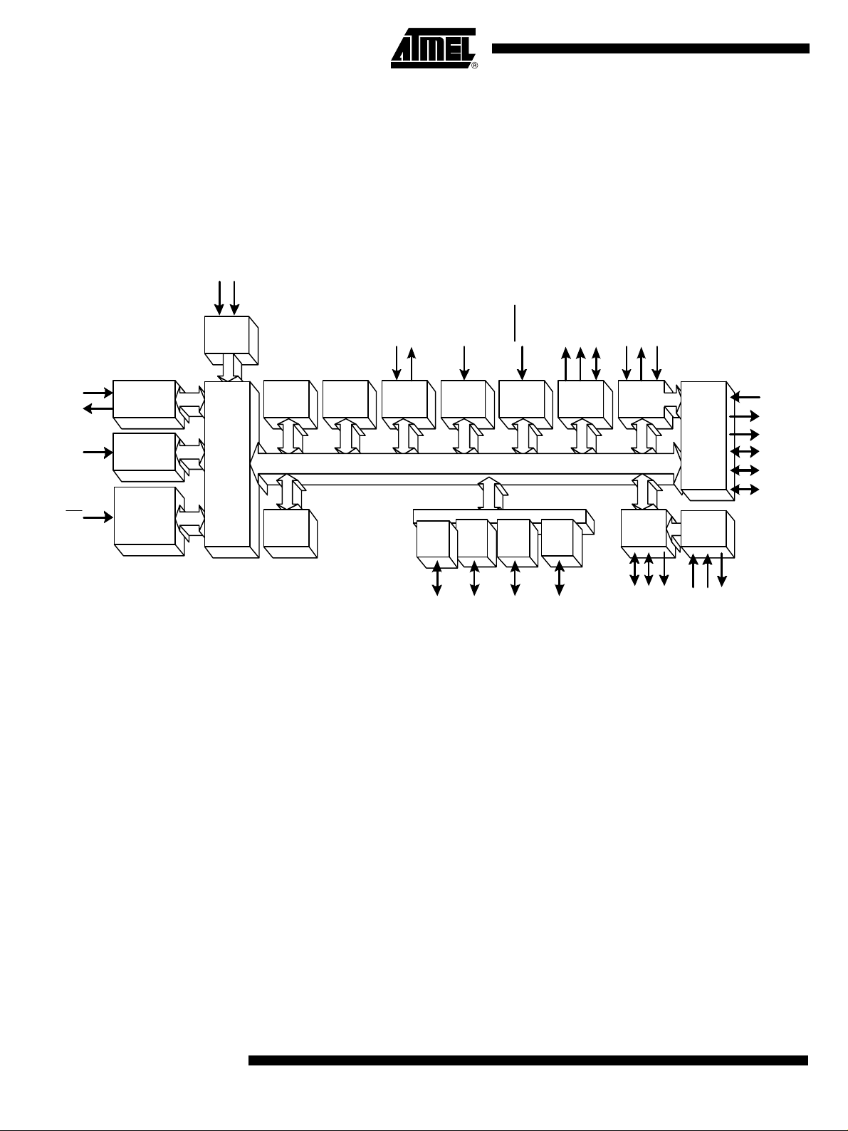
Product description AT83C5127 product is high-performance CMOS derivatives of the 80C51 8-bit micro-
controllers designed for USB smart card reader applications.
The AT83C5127 is a low pin count of the AT8xC5122 and is proposed in ROM version.
The ROM device is only factory programmable.
Block Diagram
VCC
VSS
XTA L 1
XTA L 2
RST
8 MHz
Osci llat or
PLLPLLF
WATCH-DOG
POR
PFD
RESET
3. 3 V
Regulat or
256 x 8
RAM
80C51 8-BIT CORE
256 x 8
RAM
16K x 8
ROM
512 x 8
XR A M
TxD
RxD
UART
Interface
INTERNAL ADD RESS AND DATA BUS
3-BI T
PORT
16-BI T
TI MER S
P1[2,6-7]
T[0-1]
Par all el I/O Port s
8-BI T
PORT
P3[0-7]
I nterr upt
Cont roll er
1-BI T
PORT
LI
CVCC
DC/DC
Conv ert er
USB
Interface
D+
D-
CVSS
VREF
Interface
ISO 7816
3.3V
Regulat or
AVSS
AVCC
CPRES
CRST
CCLK
CIO
CC4
CC8
DVCC
IN T[ 0-1]
P5.0
LED's
CRST1
CCLK1
Alt ernat e
Card
LED[0-3]
CIO1
2
AT83C5127
7519A–SCR–04/05
Page 3
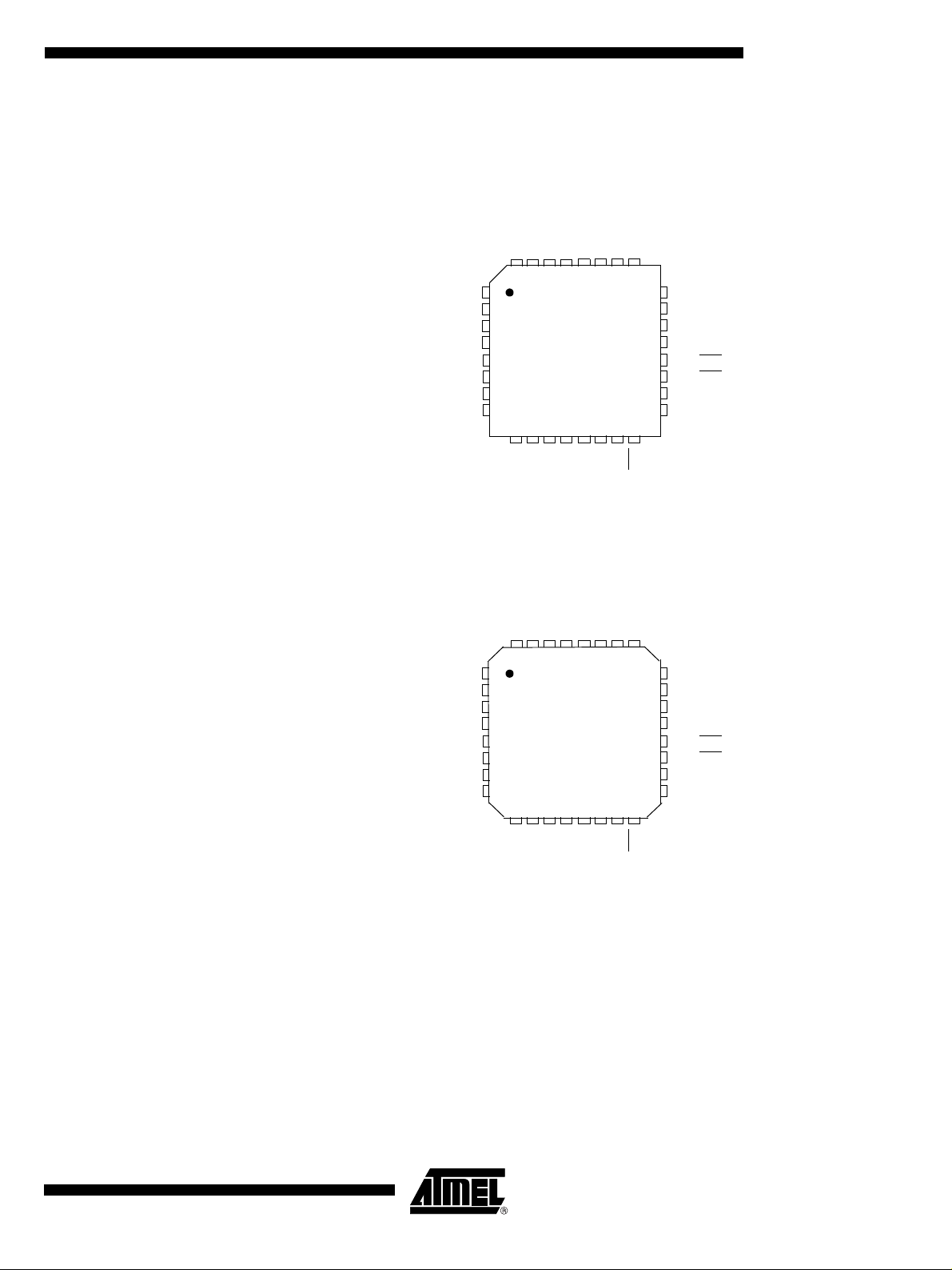
Package Description
AT83C5127
Figure 1. VQFP32 Package Pinout
CIO
DVCC
P1.2/CPRES
CC8
CRST
CC4
CCLK
P5.0
VSS
1
2
3
4
5
6
7
8
CVCC
Figure 2. MLF32 Package Pinout
CIO
DVCC
P1.2/CPRES
CC8
CRST
CC4
CCLK
P5.0
VSS
1
2
3
4
5
6
7
8
CVCC
D-D+AVC C
P1.7/CCLK1
VREF
PLLF
28 27 26
VQFP32
1211109131415
LI
VCC
P1.7/CCLK1
CVSS
VREF
P3.7/LED3
D-D+AVC C
XTAL1
XTAL2
PLLF
28 27 26
MLF32
1211109131415
LI
VCC
CVSS
XTAL1
XTAL2
P3.7/LED3
AVS S
2529303132
P3.1/TxD
24
P1.6
23
P3.0/RxD
22
P3.5/T1/CRST1
21
P3.2/INT0/LED0/CIO1
20
P3.3/INT1
19
P3.4/T0/LED1
18
P3.6/LED2
17
16
RST
AVS S
2529303132
P3.1/TxD
24
P1.6
23
P3.0/RxD
22
P3.5/T1/CRST1
21
P3.2/INT0/LED0/CIO1
20
P3.3/INT1
19
P3.4/T0/LED1
18
P3.6/LED2
17
16
RST
7519A–SCR–04/05
3
Page 4

Pin Description
Table 1. Pin Description
Port
LQFP32
Internal
Power
QFN32
Supply ESD I/O
Reset
Level Alt
Reset
Config Conf 1 Conf 2 Conf 3 Led
CIO 32 32 CVCC 6KV I/O 0 CIO Port51
CC4 3 3 CVCC 6KV I/O 0 CC8 Port51
P1.2 2 2 VCC 2KV I/O 1 CPRES Port51
CC4 5 5 CVCC 6KV I/O 0 CC4 Port51
CCLK 6 6 CVCC 6KV O 0 CCLK Push-pull
CRST 4 4 CVCC 6KV O 0 CRST Push-pull
P1.6 23 23 VCC 2KV I/O 1 Port51
P1.7 31 31 VCC 2KV I/O 1 CCLK1 Port51
P3.0 22 22 VCC 2KV I/O 1 RxD Port51 Push-pull
P3.1 24 24 VCC 2KV I/O 1 TxD Port51 Push-pull
P3.2 20 20 VCC 2KV I/O 1 INT0 Port51 LED0
P3.3 19 19 VCC 2KV I/O 1 INT1 Port51 Push-pull
CVCC inactive at reset.
ESD tested with a 10µF on CVCC
CVCC inactive at reset
ESD tested with a 10µF on CVCC
Weak & medium pull-up can be
disconnected
CVCC inactive at reset
ESD tested with a 10µF on CVCC
CVCC inactive at reset
ESD tested with a 10µF on CVCC
CVCC inactive at reset
ESD tested with a 10µF on CVCC
P3.4 18 18 VCC 2KV I/O 1 T0 Port51 Push-pull LED1
P3.5 21 21 VCC 2KV I/O 1 T1 Port51
P3.6 17 17 VCC 2KV I/O 1 Port51 LED2
P3.7 13 13 VCC 2KV I/O 1 Port51 LED3
P5.0 7 7 VCC 2KV I/O 1 Port51 Push-pull
Reset Input
The Port pins are driven to their reset conditions when a voltage lower
than V
is applied, whether or not the oscillator is running.
IL
RST
4
AT83C5127
16 16 VCC I/0
This pin has an internal 10K pull-up resistor which allows the device to
be reset by connecting a capacitor between this pin and VSS.
Asserting RST
returns the chip to normal operation.
The output is active for at least 12 oscillator periods when an internal
reset occurs.
when the chip is in Idle mode or Power-Down mode
7519A–SCR–04/05
Page 5

Table 1. Pin Description (Continued)
Internal
Power
Port
D+ 29 29 DVCC I/O
QFN32
LQFP32
Supply ESD I/O
Reset
Level Alt
USB Positive Data Upstream Port
This pin requires an external serial resistor of 33Ω and a 1.5 K
up to
Reset
Config Conf 1 Conf 2 Conf 3 Led
VREF for full speed configuration.
AT83C5127
Ω
pull-
D- 28 28 DVCC I/O
V
REF
XTAL1 14 14 VCC I
XTAL2 15 15 VCC O
PLLF 26 26 AVCC O
AVC C 27 2 7 PW R
VCC 12 12 PWR
LI 10 10 PWR
30 30 AVCC O
USB Negative Data Upstream Port
This pin requires an external serial resistor of 33Ω
USB Voltage Reference: 3.0 <
V
can be connected to D+ through a 1.5 KΩ resistor. The V
REF
voltage is controlled by software.
Input to the on-chip inverting oscillator amplifier
To use the internal oscillator, a crystal or an external oscillator must be
connected to this pin.
Output of the on-chip inverting oscillator amplifier
To use the internal oscillator, a crystal circuit must be connected to
this pin. If an external oscillator is used, leave XTAL2 unconnected.
PLL Low Pass Filter input
Receives the RC network of the PLL low pass filter.
Analog Supply Voltage
AVCC is used to supply the internal 3.3V analog regulator which
supplies the internal USB driver
Supply Voltage
VCC is used to supply the internal 3.3V digital regulator which
supplies the PLL, CPU core and internal I/O’s
DC/DC Input
LI supplies the current for the charge pump of the DC/DC converter.
- LI tied directly to VCC : the DC/DC converter must be configured in
regulator mode.
- LI tied to VCC through an external 10µH coil : the DC/DC converter
can be configured either in regulator or in pump mode.
VREF < 3.6 V
REF
CVCC 9 9 PWR
DVCC 1 1 PWR
CV SS 11 11 GN D
VSS 8 8 GND
AVSS 25 25 GND
7519A–SCR–04/05
Card Supply Voltage
CVCC is the ouput of internal DC/DC converter which supplies the
Smart Card Interface. It must be connected to an external decoupling
capacitor of 10 µF with the lowest ESR as this parameter influences
on the CVCC noise
Digital Supply Voltage
DVCC is the output of the internal analog 3.3V regulator which
supplies the USB driver. This pin must be connected to an external
680nF decoupling capacitor if the USB interface is used.
DC/DC Ground
CVSS is used to sink high shunt currents from the external coil
Digital Ground
VSS is used to supply the PLL, buffer ring and the digital core
Analog Ground
AVSS is used to supply the USB driver.
5
Page 6

Ordering Information
AT83C5127
Part Number
AT83C5127xxx-RATIM 16K ROM 4.5 - 5.5 Industrial 48 MHz / X1 LQFP32 Tray AT83C5127xxx-RATUM
AT83C5127xxx-RARIM 16K ROM 4.5 - 5.5 Industrial 48 MHz / X1 LQFP32 Tape & Reel AT83C5127xxx-RARUM
AT83C5127xxx-PUTIM 16K ROM 4.5 - 5.5 Industrial 48 MHz / X1 QFN32 Tray AT83C5127xxx-PUTUM
AT83C5127xxx-PURIM 16K ROM 4.5 - 5.5 Industrial 48 MHz / X1 QFN32 Tape & Reel AT83C5127xxx-PURUM
Memory Size
(bytes)
Supply
Voltage (V)
Temperature
Range
Max Frequency
(MHz) Package Packing
Lead free/ RoHS
Part Number
7519A–SCR–04/05
7
Page 7

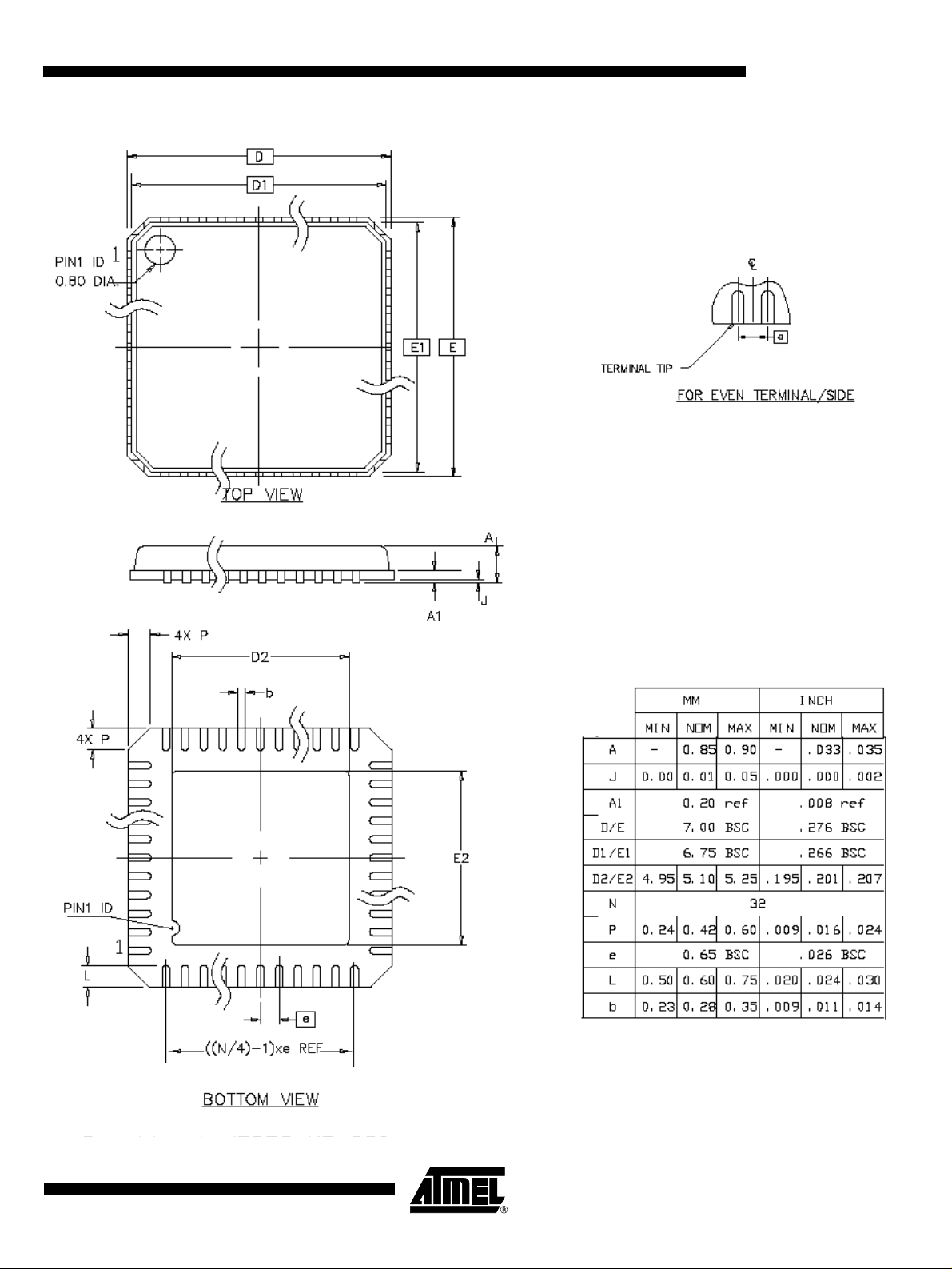
Packaging Information
LQFP32 Package
8
AT83C5127
7519A–SCR–04/05
Page 8
QFN32 Package
AT83C5127
7519A–SCR–04/05
9
Page 9

Atmel Corporation Atmel Operations
2325 Orchard Parkway
San Jose, CA 95131, USA
Tel: 1(408) 441-0311
Fax: 1(408) 487-2600
Regional Headquarters
Europe
Atmel Sarl
Route des Arsenaux 41
Case Postale 80
CH-1705 Fribourg
Switzerland
Tel: (41) 26-426-5555
Fax: (41) 26-426-5500
Asia
Room 1219
Chinachem Golden Plaza
77 Mody Road Tsimshatsui
East Kowloon
Hong Kong
Tel: (852) 2721-9778
Fax: (852) 2722-1369
Japan
9F, Tonetsu Shinkawa Bldg.
1-24-8 Shinkawa
Chuo-ku, Tokyo 104-0033
Japan
Tel: (81) 3-3523-3551
Fax: (81) 3-3523-7581
Memory
2325 Orchard Parkway
San Jose, CA 95131, USA
Tel: 1(408) 441-0311
Fax: 1(408) 436-4314
Microcontrollers
2325 Orchard Parkway
San Jose, CA 95131, USA
Tel: 1(408) 441-0311
Fax: 1(408) 436-4314
La Chantrerie
BP 70602
44306 Nantes Cedex 3, France
Tel: (33) 2-40-18-18-18
Fax: (33) 2-40-18-19-60
ASIC/ASSP/Smart Cards
Zone Industrielle
13106 Rousset Cedex, France
Tel: (33) 4-42-53-60-00
Fax: (33) 4-42-53-60-01
1150 East Cheyenne Mtn. Blvd.
Colorado Springs, CO 80906, USA
Tel: 1(719) 576-3300
Fax: 1(719) 540-1759
Scottish Enterprise Technology Park
Maxwell Building
East Kilbride G75 0QR, Scotland
Tel: (44) 1355-803-000
Fax: (44) 1355-242-743
RF/Automotive
Theresienstrasse 2
Postfach 3535
74025 Heilbronn, Germany
Tel: (49) 71-31-67-0
Fax: (49) 71-31-67-2340
1150 East Cheyenne Mtn. Blvd.
Colorado Springs, CO 80906, USA
Tel: 1(719) 576-3300
Fax: 1(719) 540-1759
Biometrics/Imaging/Hi-Rel MPU/
High Speed Converters/RF Datacom
Avenue de Rochepleine
BP 123
38521 Saint-Egreve Cedex, France
Tel: (33) 4-76-58-30-00
Fax: (33) 4-76-58-34-80
Literature Requests
www.atmel.com/literature
Disclaimer: The information in this document is provided in connection with Atmel products. No license, express or implied, by estoppel or otherwise, to any
intellectual property right is granted by this document or in connection with the sale of Atmel products. EXCEPT AS SET FORTH IN ATMEL’S TERMS AND CONDI-
TIONS OF SALE LOCATED ON ATMEL’S WEB SITE, ATMEL ASSUMES NO LIABILITY WHATSOEVER AND DISCLAIMS ANY EXPRESS, IMPLIED OR STATUTORY
WARRANTY RELATING TO ITS PRODUCTS INCLUDING, BUT NOT LIMITED TO, THE IMPLIED WARRANTY OF MERCHANTABILITY, FITNESS FOR A PARTICULAR
PURPOSE, OR NON-INFRINGEMENT. IN NO EVENT SHALL ATMEL BE LIABLE FOR ANY DIRECT, INDIRECT, CONSEQUENTIAL, PUNITIVE, SPECIAL OR INCIDENTAL DAMAGES (INCLUDING, WITHOUT LIMITATION, DAMAGES FOR LOSS OF PROFITS, BUSINESS INTERRUPTION, OR LOSS OF INFORMATION) ARISING OUT
OF THE USE OR INABILITY TO USE THIS DOCUMENT, EVEN IF ATMEL HAS BEEN ADVISED OF THE POSSIBILITY OF SUCH DAMAGES. Atmel makes no
representations or warranties with respect to the accuracy or completeness of the contents of this document and reserves the right to make changes to specifications
and product descriptions at any time without notice. Atmel does not make any commitment to update the information contained herein. Atmel’s products are not
intended, authorized, or warranted for use as components in applications intended to support or sustain life.
© Atmel Corporation 2005. All rights reserved. Atmel®, logo and combinations thereof, are registered trademarks, and Everywhere You Are
is the trademarks of Atmel Corporation or its subsidiaries. Other terms and product names may be trademarks of others.
Printed on recycled paper.
7519A–SCR–04/05
SM
 Loading...