

Page 1

Features
• 5 Smart Card Interfaces
– Compliance with ISO 7816, EMV2000, GIE-CB and GSM Standards
– Direct Connection to the Smart Cards
Logic Level Shifters
Short Circuit Current Limitation
4kV+ ESD Protection (MIL/STD 883 Class 3)
– 1 or 2 Master Smart Card interfaces
Synchronous Card support (with C4 and C8 Contacts)
Card Detection and Automatic de-activation sequence on card extraction
– 1 to 4 SAM/SIM cards (15 to 30mA each)
– Programmable Voltage for each smart card
Class A: 5V ±0.4V at 60 mA (±0.25V at 65 mA with VCC= 5V±10%)
Class B: 3V ±0.2V at 60 mA
Class C: 1.8V ±0.14V at 40mA
– Low Ripple Noise: < 200 mV
– Programmable Activation Sequence
– Automatic de-activation on card power-fail or over-current and system power-fail
– Card Clock Stop High or Low for Card Power-down Modes
• Versatile Host Interface
– Two Wire Interface (TWI) Link at 400kbit/s
Programmable Address allow up to 4 AT83C26 on the bus
– Programmable Interrupt Output
• Reset Output Includes
– Power-On Reset (POR)
– Power-Fail Detector (PFD)
• Extended Voltage Operation: 3 to 5.5V
• Low Power Consumption
– 5 mA Maximum Operating Current (without Smart Card)
– 150 mA Maximum In-rush Current (each DC/DC)
–30 µA Typical Power-down Current (without Smart Card)
• 4 to 48 MHz Clock Input
• System clock derived from the external clock input
• Industrial Temperature Range: -40 to +85°C
• Packages: QFN48, VQFP48
Smart Card
Reader
Interface With
Power
Management
AT83C26
Description
The AT83C26 is a smart card reader interfac e IC for s mart c ard re ade r/ writer a pplic ations such as EFT/POS terminal s and set top boxes. It enable s the management of
any type of smart card from any kind of host. Up to 4 AT83C26 can be connected in
parallel thanks to the programmable TWI address.
Its high efficiency DC/DC con verters and low quiesce nt current i n stand-by mod e
make it particularly suited to lo w power an d portable a pplicati ons. The red uced bil l of
material allows to lower significantly the system size and cost. A sophisticated protection system guarantees timely and controlled shutdown upon error conditions.
7511B–SCR–10/05
Page 2
AT83C26
Acronyms
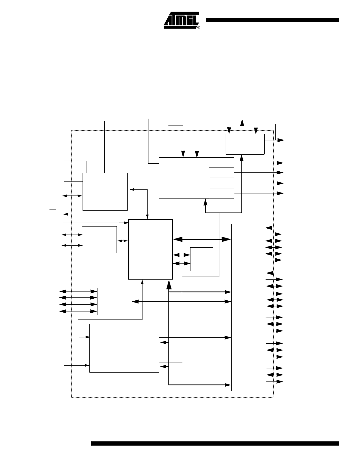
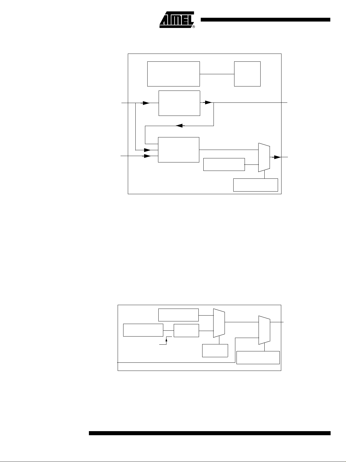
Block Diagram
TWI: Two Wire Interface
POR: Power On Reset
PFD: Power Fail Detect
ART: Automatic Reset Transition
ATR: Answer To Reset
BYPASS
EVCC
RESET
INT
A2/CK, A1/RST
SCL
SDA
I/O1
I/O2
AUX1
AUX2
VCC
VSS
Voltage
supervisor
POR/PFD
TWI
Controller
I/0
Selection
CVSSB
CVCCB
Main
Control
& Logic Unit
CVCCINB
LIB
DC/DC
Converter B
Timer
16 bits
LDO
LDO
LDO
LDO
CVSS1
LIA
DC/DC
Converter A
smart
card 1
smart
card 2
Analog
Drivers
SAM/SIM 1
CVCCIN1
CVCC1
CVCC2
CVCC3
CVCC4
CVCC5
CPRES1
CRST1
CIO1
CC41
CC81
CCLK1
CPRES2
CRST2
CIO2
CCLK2
CC42, see (1)
CC82, see (1)
CRST3, see (1)
CIO3, see (1)
CCLK3
SC1
SC2
SC3
2
CLK
Clock Circuit CCLK
Clock Controller
SAM/SIM 2
SAM/SIM 3
CRST4
CIO4
CCLK4
CRST5
CIO5
CCLK5
SC4
SC5
Note: 1. CRST3/CC82 are on the same pin. CIO3/CC42 are on the same pin. If complete Smart card 2
interface is used, SAM/SIM3 isn’t available. Respectively, if SAM/SIM3 is used, complete
Smart card 2 isn’t available.
7511B–SCR–10/05
Page 3
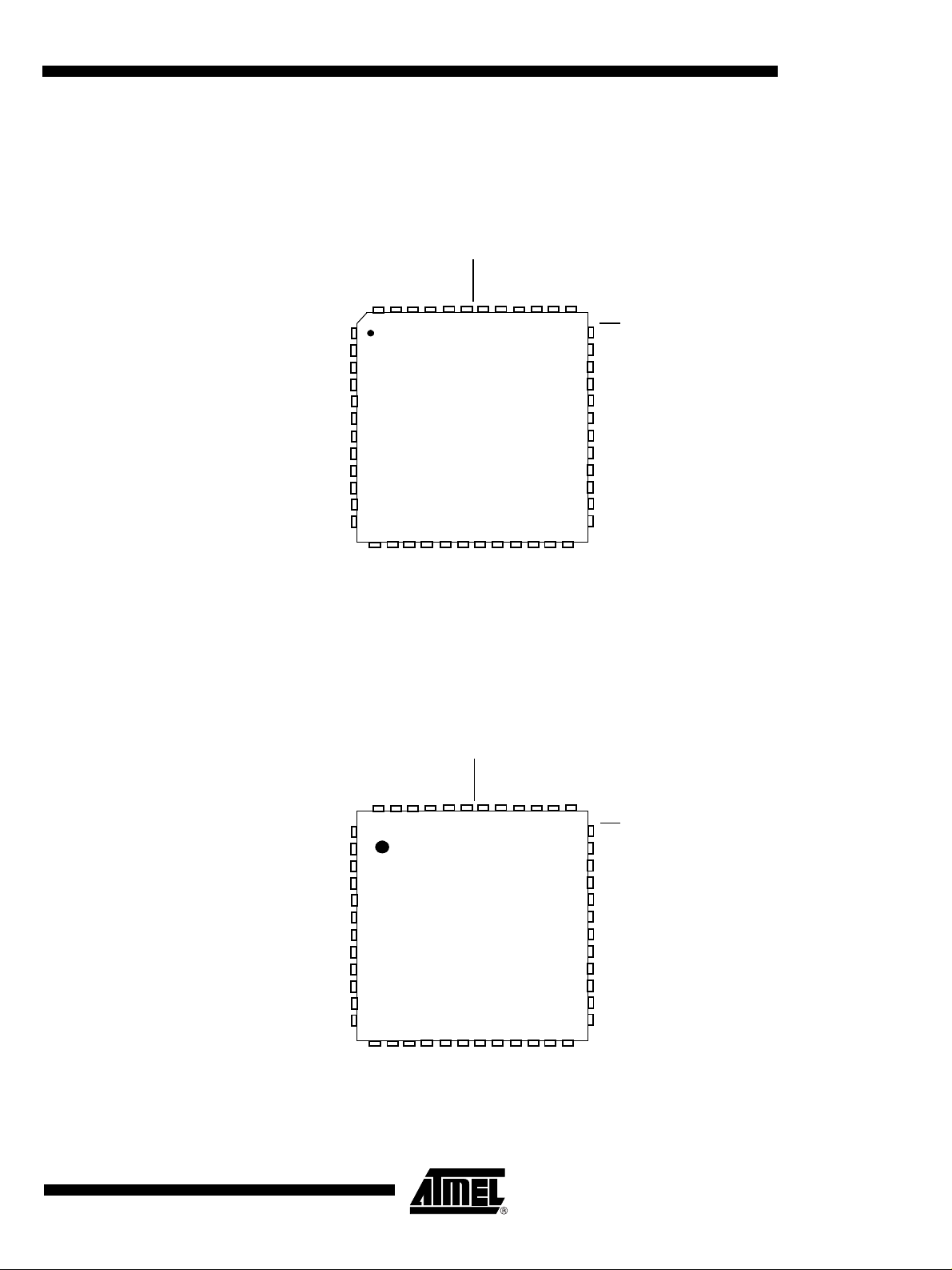
Pin Description
Pinout (Top View)
AT83C26
VQFP48 Pinout
CVCC3
CRST3/CC82
CCLK3
CIO3/CC42
CVCC4
CRST4
CCLK4
CIO4
CIO5
CCLK5
CRST5
CVCC5
QFN48 Pinout
CIO2
CRST2
CCLK2
4748
1
2
3
4
5
6
7
8
9
10
11
12
46
13 14 15 16 17
CIO1
CC81
CC41
CVCC2
CVCCINB
4445
VQFP 48
TOP VIEW
18 19 20
CCLK1
CRST1
ESET
R
CPRES2
4243
CPRES1
CVCCIN1
CVCCB
CVCCB
39
40
41
21 22 23 24
CVCC1
CVCC1
EVCC
LIB
CVSSB
37
38
36
I
NT
CLK
35
34
A2/CK
A1/RST
33
AUX1
32
31
AUX2
IO1
30
IO2
29
SCL
28
SDA
27
26
BYPASS
VSS
25
LIA
VCC
CVSS1
7511B–SCR–10/05
CVCC3
CRST3/CC82
CCLK3
CIO3/CC42
CVCC4
CRST4
CCLK4
CIO4
CIO5
CCLK5
CRST5
CVCC5
CIO2
CCLK2
4748
1
2
3
4
5
6
7
8
9
10
11
12
46
13 14 15 16 17
CIO1
CC81
CC41
CRST2
CCLK1
CVCCINB
CVCC2
4445
QFN 48
TOP VIEW
18 19 20
CRST1
CVCCIN1
CPRES2
4243
ESET
R
CVCCB
41
21 22 23 24
CVCC1
CPRES1
40
CVCCB
39
CVCC1
EVCC
LIB
CVSSB
37
38
36
INT
35
CLK
34
A2/CK
33
A1/RST
32
AUX1
31
AUX2
30
IO1
29
IO2
28
SCL
SDA
27
26
BYPASS
25
VSS
LIA
VCC
CVSS1
3
Page 4
AT83C26
Signals
Table 1. Ports Description
VQFP48 or
QFN48
Pin number
1 CVCC3 4kV+ PWR VCC pin for SC3 interface.
Pad Name Pad Internal
Power Supply
ESD
Limits
Pad T y pe Description
2 CRST3/CC82 CVCC3 4kV+
3 CCLK3 CVCC3 4kV+ O CCLK pin for SC3 interface.
4 CIO3/CC42 CVCC3 4kV+
5 CVCC4 4kV+ PWR VCC pin for SC4 interface.
6 CRST4 CVCC4 4kV+ O RST pin for SC4 interface.
7 CCLK4 CVCC4 4kV+ O CCLK pin for SC4 interface.
8 CIO4 CVCC4 4kV+
9 CIO5 CVCC5 4kV+
10 CCLK5 CVCC5 4kV+ O CCLK pin for SC5 interface.
11 CRST5 CVCC5 4kV+ O RST pin for SC5 interface.
12 CVCC5 4kV+ PWR VCC pin for SC5 interface.
13 CC81 CVCC1 4kV+
I/O
pull up
I/O
pull up
I/O
pull up
I/O
pull up
I/O
pull up
See SC2_CFG1 register:
If SC2_FULL bit = 0, CRST pin for SC3 interface.
If SC2_FULL bit = 1, CC8 pin for SC2 interface.
See SC2_CFG1 register:
If SC2_FULL bit = 0, CIO pin for SC3 interface.
If SC2_FULL bit = 1, CC4 pin for SC2 interface.
CIO pin for SC4 interface.
CIO pin for SC5 interface.
CC8 pin for SC1 interface.
14 CC41 CVCC1 4kV+
15 CIO1 CVCC1 4kV+
16 CCLK1 CVCC1 4kV+ O CCLK pin for SC1 interface.
17 CRST1 CVCC1 4kV+ O RST pin for SC1 interface.
18 CVCCIN1 4kV+ PWR This pin must be connected to CVCC1 pins next to the package.
19 CPRES1 VCC 4kV+
20 CVCC1 4kV+ PWR
21 CVCC1 4kV+ PWR VCC pin for SC1 interface.
4
I/O
pull up
I/O
pull up
I
pull up
CC4 pin for SC1 interface.
CIO pin for SC1 interface.
Card presence for SC1 interface.
An internal pull up to VCC can be activated in the pad if necessary using
PULLUP1 bit in SC1_CFG1 register (activated by default).
VCC pin for SC1 interface.
The two CVCC1 pins are connected together near the package. Only one
wire goes to the smart card connector. The reason of two CVCC1 pins is
to reduce noise.
7511B–SCR–10/05
Page 5
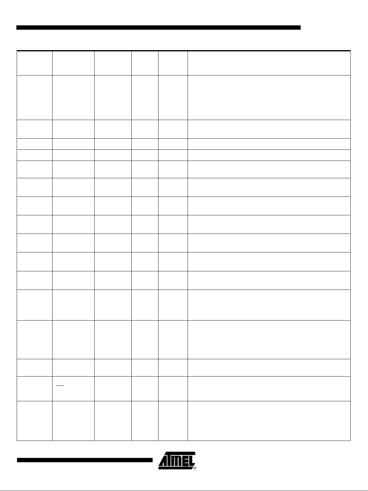
Table 1. Ports Description (Continued)
VQFP48 or
QFN48
Pin number
22 LIA 2kV PWR
Pad Name Pad Internal
Power Supply
ESD
Limits Pad Type Description
AT83C26
DC/DCA input.
LIA must be tied to VCC pin through an external coil (typically 10µH) and
provides the current for the charge pump of the DC/DCA converter.
It may be directly connected to VCC if the step-up converter is not used
(see STEPREGA bit in SC1_CFG4 register and see minimum VCC
values in T able 50.for class A and Table 51. for class B)
23 CVSS1 2kV GND
24 VCC 2kV PWR VCC is used to power the internal voltage regulators and I/O buffers.
25 VSS 2kV GND Ground.
26 BYPASS VCC 2kV I
27 SDA VCC 2kV
28 SCL VCC 2kV
29 IO2 EVCC 2kV
30 IO1 EVCC 2kV
31 AUX2 EVCC 2kV
32 AUX1 EVCC 2kV
33 A1/RST EVCC 2kV I
I/O
open drain
I/O
open drain
I/O
pull up
I/O
pull up
I/O
pull up
I/O
pull up
DC/DCA input.
This pin must be directly connected to the VSS of power supply.
A high level on this pin activates a low power consumption mode with
internal regulator bypassed.
Micro controller interface function: TWI serial data.
An external pull up must be connected on SDA pin (4.7kOhms).
Micro controller interface function: TWI clock.
An external pull up must be connected on SCL pin (4.7kOhms).
The behavior of this pin depends on IOSEL[3/0] bits values (see
IO_SELECT register).
The behavior of this pin depends on IOSEL[3/0] bits values (see
IO_SELECT register).
The behavior of this pin depends on IOSEL[3/0] bits values (see
IO_SELECT register).
The behavior of this pin depends on IOSEL[3/0] bits values (see
IO_SELECT register).
The TWI address depends on the value present on this pin at reset.
If CRST transparent mode is selected, the A1/RST signal is connected to
CRST1 or CRST2 pins (see CRST_SEL1 and CRST_SEL2 bits
respectively in SC1_CFG4 and SC2_CFG2 registers).
34 A2/CK EVCC 2kV I
35 CLK EVCC 2kV I Master clock.
36 INT VCC 2kV
37 EVCC PWR
7511B–SCR–10/05
O
open drain
The TWI address depends on the value present on this pin at reset.
If CCLKn transparent mode is selected, the A2/CK signal is connected to
CCLKn pins (with n=1 to 5).
See CKSn[2:0] bits respectively in SC1_CFG1, SC2_CFG2, SC3_CFG2,
SC4_CFG2, SC5_CFG2 registers.
Interruption status.
An internal pull up to VCC can be activated in the pin if necessary using
INT_PULLUP bit in SC1_CFG4 (deactivated by default).
Extra supply voltage (Micro controller power supply).
EVCC is used to supply the internal level shifters of host interface pins.
EVCC is connected to the host power supply.
EVCC voltage can be directly connected to VCC if the host power supply
and the AT83C26 power supply is the same.
5
Page 6
AT83C26
Table 1. Ports Description (Continued)
VQFP48 or
QFN48
Pin number
Pad Name Pad Internal
Power Supply
ESD
Limits Pad Type Description
38 CVSSB GND
39 LIB 2kV PWR
40 CVCCB 2kV PWR
41 CVCCB 2kV PWR DC/DCB output.
42 RESET VCC 2kV
43 CPRES2 VCC 4kV+
44 CVCCINB PWR This pin must be connected to CVCCB pins next to the package.
I/O
open drain
pull up
DC/DCB input.
This pin must be directly connected to the VSS of power supply.
DC/DCB input.
LIB must be tied to VCC pin through an external coil (typically 10µH) and
provides the current for the charge pump of the DC/DCB converter.
It may be directly connected to VCC if the step-up converter is not used
(see STEPREGB bit in DCDCB register and see minimum VCC values in
Table 53.for class A and Table 54. for class B)
DC/DCB output.
The two CVCCB pins are connected together near the package. CVCCB
pin is only used for DC/DCB voltage measurements.The reason of two
CVCCB pins is to reduce noise.
Micro controller interface function: reset signal.
• power on reset
• A low level on this pin keeps the AT83C26 under reset even if
applied on power-on. It also resets the AT83C26 if applied when the
AT83C26 is running.
• Asserting RESET
Card presence for SC2 interface.
I
An internal pull to VCC can be activated in the pad if necessary using
PULLUP2 bit in SC2_CFG1 register (activated by default).
45 CVCC2 4kV+ PWR VCC pin for SC2 interface.
46 CRST2 CVCC2 4kV+ O CRST pin for SC2 interface.
47 CCLK2 CVCC2 4kV+ O CCLK pin for SC2 interface.
48 CIO2 CVCC2 4kV+
I/O
pull up
CIO pin for SC2 interface.
6
7511B–SCR–10/05
Page 7
Pad Type Description
To simplify the understanding of Figure 1. to F igure 8., a shortcut is possible by replacing the
weak transistor by a 100k Ohms pull-up resistor, the medium transistor by a
10k Ohms pull-up resistor and the strong transistor by a 1k Ohms pull-up resistor.
Input/Output with Pull-up Configuration (IO1, IO2, AUX1, AUX2)
This output type can be used as both an inpu t and output withou t the need to r econfigure the
port. This is possible because when the port outputs a logic high, it is weakly driven, allowing an
external device to pull the pin low. When the port outputs a logic low state, it is driven strongly
and able to sink a fairly large current.
Figure 1. Input/Output with Pull-up Configuration
AT83C26
2 DCCLK
CLOCK DELAY
P
Strong
P
Keep
PMOS
Port latch
Data
N
Pin
NMOS
Input
Data
Input/Output with Pull-up Configuration (CIOn with n = 1, 2, 3, 4, 5) and (CC4n, CC8n with n = 1,
2)
Figure 2. Input/Output with Pull-up Configuration
PMOS
N
P
Strong
P
Medium
Slew control
with
CIOn_SLEW_CTRL bits
(n= 1 to 5)
Pin
Port latch
Data
2 DCCLK
CLOCK DELAY
NMOS
7511B–SCR–10/05
Input
Data
7
Page 8

AT83C26
Input/Output with Open Drain Configuration (SDA, SCL, RESET)
Figure 3. Input/Output with Open Drain Configuration
Data
NPort latch
NMOS
Input
Data
Output Configuration (CCLKn with n = 1, 2, 3, 4, 5)
Figure 4. Output Configuration
P
Strong
PMOS
Port latch
Data
N
NMOS
Slew control
with
CIOn_SLEW_CTRL bits
Pin
Pin
Output Configuration (CRSTn with n = 1, 2, 3, 4, 5)
Figure 5. Output Configuration
Port latch
Data
8
P
Strong
PMOS
Pin
N
NMOS
7511B–SCR–10/05
Page 9
Open drain Output with programmable pull-up Configuration (INT)
Figure 6. Open Drain Output with programmable pull-up
AT83C26
Port latch
Data
Input Configuration (A1, A2, CLK, BYPASS)
Figure 7. Input
Input
Data
INT_PULLUP bit
NMOS
P
Weak
Pin
N
Pin
Input with programmable pull-up Configuration (CPRES1, CPRES2)
Figure 8. Input with programmable pull-up
INT_PULLUP bit
Input
Data
P
Weak
Pin
7511B–SCR–10/05
9
Page 10

AT83C26
Operational Modes
TWI Bus Control The Atmel Two-wire Inter fac e (T WI ) interc onn ec ts c omp one nts on a un iqu e two-wi re bus, mad e
up of one clock line and one data line with s peeds of up to 400 K bits per se cond, based on a
byte-oriented transfer format.
The TWI-bus interface can be used:
– To configure the AT83C26
– To select interface
– To select the operating mode of the card: 1.8V, 3V or 5V
– To configure the automatic activation sequence
– To start or stop sessions (activation and de-activation sequences)
– To initiate a warm reset
– To control the clock to the card in active mode
– To control the clock to the card in stand-by mode (stop LOW, stop HIGH or running)
– To enter or leave the card stand-by or power-down modes
– To select the interface (connection to the host I/O/C4/C8)
– To request the status (card present or not, over-current and out of range supply
voltage occurrence)
– To drive and monitor the card contacts by software
– To accurately measure the ATR delay when automatic activation is used
– Re-use the AT83C24 command set for the first DC/DC and smart card interface with
the following changes:
•CKS extended to CONFIG2[0:3], CKS=8 selects CLK/3 and CKS>8 is reserved
•The slave address byte for TWI write commands is 0100 A2A110 and 0100 A2A111
for TWI read commands
TWI Commands
Frame Structure The structure of the TWI bus data frames is made of one or a series of write and read com-
mands completed by STOP.
Write commands to the AT83C26 have the structure:
ADDRESS BYTE + COMMAND BYTE + DATA BYTE(S)
Read commands to the AT83C26 have the structure:
ADDRESS BYTE + DATA BYTE(S)
The ADDRESS BYTE is sampled on A2/CK and A1/RST after each reset (hard/sof t/g en er a l
call) but A2/CK, A1/RST can be used for transparent mode after the reset.
10
7511B–SCR–10/05
Page 11
Figure 1. Data transfer on TWI bus
SDA
Address byte
AT83C26
acknowledgement
from slave
command
and/or data
SCL
123456
start condition
78
9
stop condition
Address Byte The first byte to send to the device is the address byte. The device controls if the hardware
address (A2/CK, A1/RST pins on reset) corresponds to the address given in the address byte
(A2, A1 bits).
If the level is not stable on A2/CK pin at reset, the user has to manage the possible address
taken by the device.
Figure 2. Address Byte
b7 b6 b5 b4 b3 b2 b1 b0
1
0
0
0A2
A1
R/W
1
7511B–SCR–10/05
Slave Address on 7 Bits
1 for READ Command
0 for WRITE Command
Up to 4 devices can be connected on the same TWI bus. Each device is configured with a different combination on A2/CK, A1 /RST pins. The address by te of each device for read/wri te
operations are listed below.
Table 2. Address Byte Values
A2
(A2/CK pin)
0 0 0x43 0x42
0 1 0x47 0x46
1 0 0x4B 0x4A
1 1 0x4F 0x4E
A1
(A1/RST pin)
Address Byte
for
Read
Command
Address Byte
for
Write
Command
11
Page 12
AT83C26
RESET pin
The TWI ADDRESS BYTE is sampled on A2/CK and A1/RST after a rising edge on RESET pin.
The delay between the rising edge and the sampling of A2/CK and A1/RST is t1.
The value for t1 is 22 CLK period.
The minimum value for t2 is 40 CLK period. During the t2 time, the TWI bus is not ready to
receive a command.
The CLK period depends on the frequency of the signal on CLK pin.
The RESET pin is an I/O with Open Drain. The host IO pin connecte d to RESET must be an I/O
with open drain (with external pull-up) or an I/O with internal pull up (without external pull-up).
Figure 3. Timings after reset
Sampling of TWI address
t1
RESET
BYPASS pin
A high level on this pin activates a low power consumption mode.
At reset, the level on this pin must be fixed (VSS or VCC).
Before to set BYPASS pin, SHUTDOWNA and SHUTDOWNB bits must be set.
If SHUTDOWNA bit is set, DCDCA is switched off.
If SHUTDOWNB bit is set, DCDCB is switched off.
If SHUTDOWNA and SHUTDOWNB bits are set, the regulator is switched off.
If BYPASS pin is at a high level, the bandgaps are switched off.
Smart Card Interfaces
The AT83C2 6 enable s the ma nageme nt of up to 5 smart c ard inte rfaces . Due to s hared IOs
between SC2 and SC3, the user should choose between a full SC2 interface (with CC4 and
CC8) or SC3 interfa ce.
SDA
t2
Address byte
12
The SC2_FULL bit in SC2_CFG1 register is used to select the SC2/S C3 interfaces
configuration.
7511B–SCR–10/05
Page 13

Table 3. SC2 and SC3 shared IOs
AT83C26
Pin name
CPRES2
CRST2
CIO2
CCLK2
CRST3/CC82
CIO3/CC42
CCLK3
SC2_FULL = 1
SC3 interface not available
CPRES2
CRST2
CIO2
CCLK2
CC82
CC42
unused
DCDC Converters
SC2_FULL = 0
SC2 without CC4and CC8 + SC3 interface
CPRES2
CRST2
CIO2
CCLK2
CRST3
CIO3
CCLK3
The DC/DC A converter is used to provide smart card voltage for the SC1 interface (CVCC1).
The DC/DC B converter i s used to provi de sm art car d volt age for the SCn int erfac es (n=2 , 3, 4,
5).
DC/DC converters need a clock of 4MHz (see Section “Clock Controller”). Two internal oscilla-
tors (one for each converter) provide the DC/DC clocks.
The DC/DCB output is connected on 4 LDO regulators (Low Drop Output) to generate CVCCn
voltage (n=2, 3, 4, 5).
Clock Controller
The clock controller outputs six clocks:
1. Five clocks for CCLK1, CCLK2, CCLK3, CCLK4 and CCLK5. Four different sources can
be used: CLK pin, DCCLK signal, CARDCKn bit (n=1, 2, 3, 4, 5) or A2/CK.
2. A DCCLK clock used for pads and deactivation sequence.
Clock controller for SCn (n=1, 2, 3, 4, 5)
The transparent mode with A2/CK pin is available on SCn interface. The CKSn[2:0] register is
used to select this transparent mode between A2/CK and CCLKn. The bi t CKSTOPn must be
cleared to have CCLKn running according to CKSn[2:0].
7511B–SCR–10/05
13
Page 14
AT83C26
Figure 4. Clock Block Diagram with Software Activation
CRST controller
CRSTn for SCn interface (n=1, 2)
CLK
A2/CK
Internal
oscillators
DCK[2:0]
CKSn[2:0]
DC/DCA
and B
CARDCKn bit
CKSTOPn bit
DCCLK
0
1
CCLKn
The CRSTn output pin is driven by the CARDRSTn bit value or by A1/RST pin.
Three modes are available:
• If the ARTn bit is reset, CRSTn pin is driven by CARDRSTn bit.
• If the ARTn bit is set, CRSTn pin is controlled and follows the “Automatic Reset Transition”
(see Activation sequence page 25).
• A transparent mode with A1/RST pin.
Figure 5. CRSTn Block Diagram
A1/RST
CARDRSTn bit
CARDRSTn bit
tb delay
0
1
ARTn bit
0
1
CRST_SELn bit
CRSTn
14
7511B–SCR–10/05
Page 15
CRSTn for SCn interface (n= 3, 4, 5)
1
The CRSTn output pin is driven by the CARDRSTn bit value (see SCn_CFG2 register).
Two modes are available:
• If the ARTn bit is reset, CRSTn pin is driven by CARDRSTn bit.
• If the ARTn bit is set, CRSTn pin is controlled and follows the “Automatic Reset Transition”
(see Activation seque nce page 25).
Figure 6. CRSTn Block Diagram
AT83C26
CARDRSTn bit tb delay
If SC2_FULL=1, the SC3 interface is not available.
CIO, CC4, CC8 controller
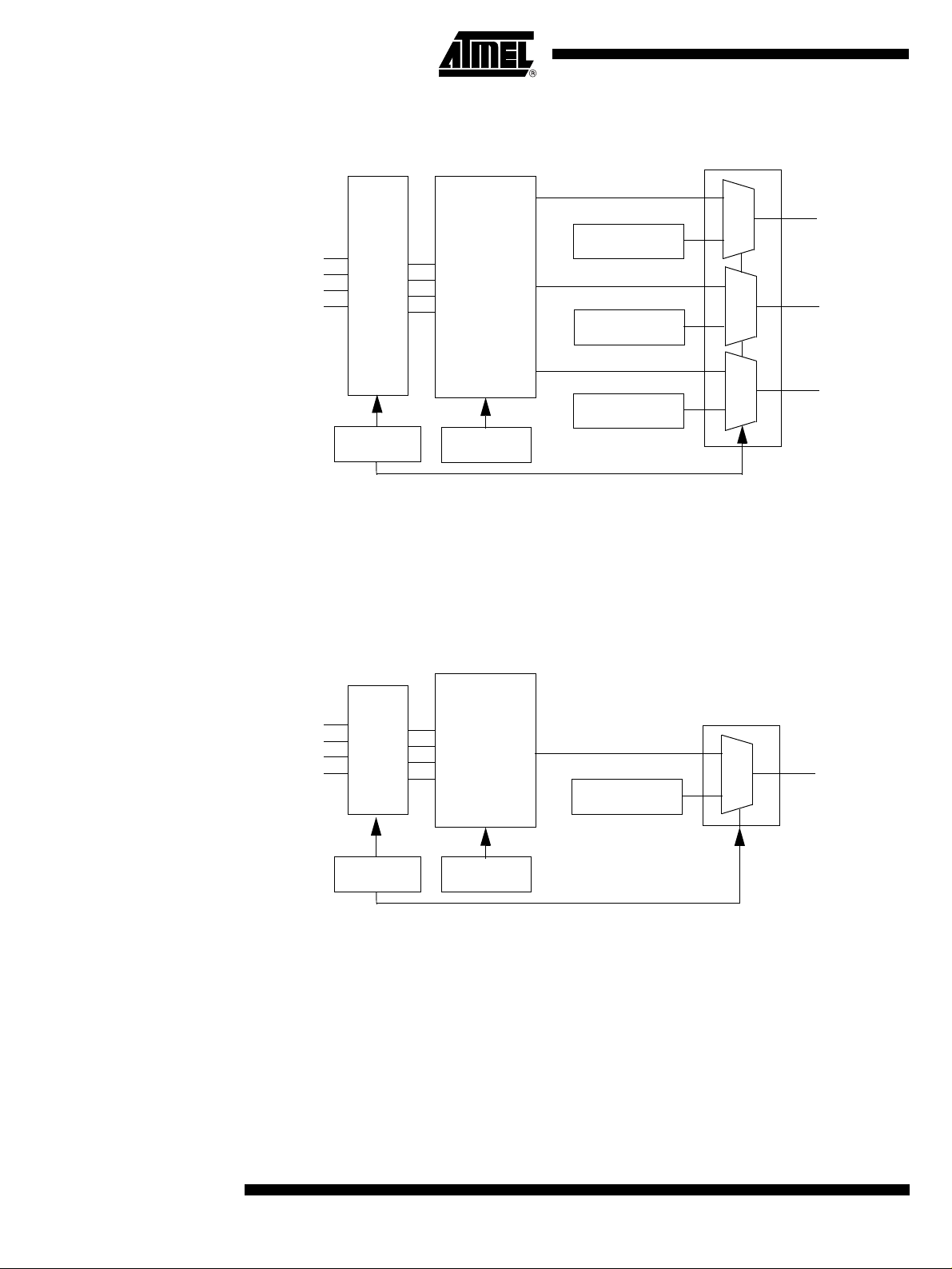
CIO1, CC41, CC81 controller for SC1 interface
The CIO1, CC41, CC81 output pins are driven respectively by CARDIO1, CARDC41, CARDC81
bits values or by I/O1, I/O2, AUX1or AUX2 signals. This selection depends of the IODIS1 bit
value (SC1_INTERFACE register) and of IOSEL[3:0] bits value (IO_SELECT register).
Figure 7. CIO1, CC41, CC81 Block Diagram
IO1
IO2
AUX1
AUX2
HiZ
control
CARDRSTn bit
Multiplex
0
1
ARTn bit
CARDIO1 bit
CARDC41 bit
CRSTn
0
CIO1
1
0
CC4
1
7511B–SCR–10/05
0
CARDC81 bit
IODIS1 bit
If IODIS1 is set, the CARDIO1 bit value is output on CIO1.The input selected by IOSEL for CIO1
is in High impedance state. CC41 and CC81 have the same behavior.
If IODIS1 is reset, data are bidirectional between the I/O1, I/O2, AUX1, AUX2 pins (see
IO_SELECT register) and CIO1, CC41, CC81 pins.
IOSEL[3:0]
1
CC81
15
Page 16
AT83C26
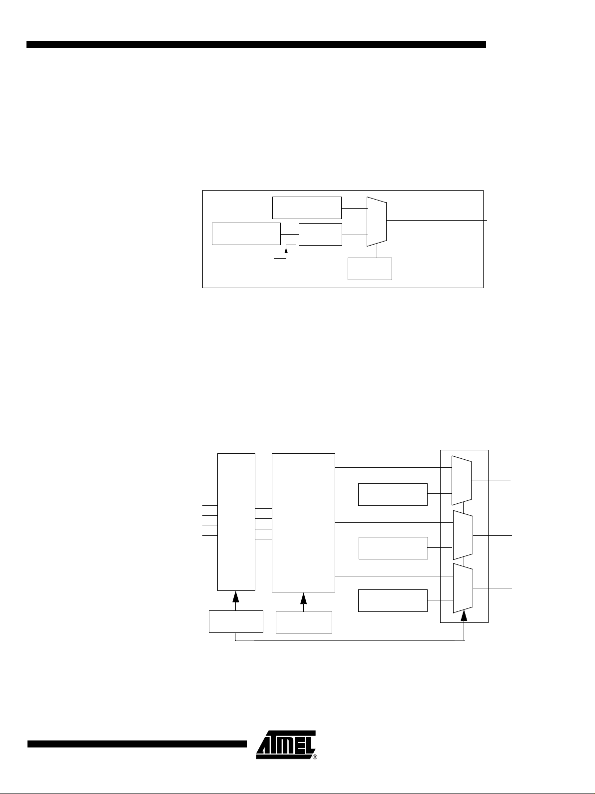
CIO2, CC42, CC82 controller for SC2 interface
2
Figure 8. CIO2, CC42, CC82 Block Diagram
IO1
IO2
AUX1
AUX2
The SC2_FULL bit must be set to use CC42 and CC82.
CIOn controller for SCn interface (n=3, 4, 5)
The CIOn output pin is driven by CARDIOn bit values or by I/O1, I/O2, AUX1 or AUX2 signals.
This selection depends of the IODISn bit value. If IODISn is reset, data are bidirectional between
the I/O1, I/O2, AUX1, AUX2 pins (see IO_SELECT register) and CIOn pins.
Figure 9. CIOn Block Diagram
HiZ
control
IODIS2 bit
Multiplex
IOSEL[3:0]
CARDIO2 bit
CARDC42 bit
CARDC82 bit
0
1
0
1
0
1
CIO2
CC4
CC82
IO1
IO2
AUX1
AUX2
CIOn (n=1 to 5), CC41, CC81, CC42, CC82 transparent mode description
Two modes are available on CIOn, CC4n, CC8n signals:
• Bit control (a bit controls the output pin)
• Transparent mode (IO signal and CIO are linked after level shifter)
According to IO_SELECT register value and IODISn bits values, one of 4 input pins (IO1, IO2,
AUX1 or AUX2) is linked to the selected output.
The idle state is the high level. Each signal is bidirectional.
HiZ
control
IODISn bit
Multiplex
IOSEL[3:0]
CARDIOn bit
0
CIOn
1
16
7511B–SCR–10/05
Page 17
T ransparent mode arbitration system
The first between IO and CIO to force a low level becomes the master.
The slave signal is grounded after t1 delay:
t1 max = 2* (CLK period).
Figure 10. Bidirectional mode
AT83C26
IO
CIO
t1
master
t2
slave
t1
t1
slave
master
t1
The minimum delay for a puls e at 0 or 1 to b e detected is between 0.5 and 1.5 CLK peri od
(depending on arrival time).
If IO and CIO are both grounded, CIO becomes the master.
The minimum delay to switch of master without electrical conflict is equal to:
t2 min = 4 * (CLK period) + 2 * (DCCLK period) * (CLK period).
If a master switch appears before this minimum delay, the electrical conflict delay is:
t2 = 2 * (DCCLK period) * (CLK period)
Figure 11. Electrical conflict
7511B–SCR–10/05
CIO
IO
master
slave
CIO pad becomes output
slave
t2
master
t1
17
Page 18

AT83C26
CCLKn and CIOn (n=1 to 5) slew rate control
Three registers SLEW_CTRL_1, SLEW_CTRL_2 and SLEW_CTRL_3 control the slew rate of
the CIOn and CCLKn signals. Each signal has 2 control bits.
An automatic mode is proposed. The VCARDn[1:0] value is used to automatically adjust the
slew rate.
For specific cases, like long wires between AT83C26 and smart card connector for example, the
user can forced the slew rate.
The rising edge and the falling edge are modified with the slew rate control for CCLKn.
Only the rising edge is modified on CIOn with the slew rate control.
See Table 63. to Table 68. in Electrical Characteristics.
18
7511B–SCR–10/05
Page 19
Card Presence Detection
Card presence detection for SC1 interface
The card presence si gnal is conn ected on th e CPRES1 pin . The polari ty of card pres ence contact is selected with the CARDDET1 bit (see SC1_CFG1 register). A programmable filtering is
controlled with the CDS1[2-0] bits.
The internal pull-up on the CPRES1 pin can be disconnected in order to reduce the consumption. An external pull-up mu st be con nected to V c c. The PULLUP1 bit (see SC1_CFG1 registe r)
controls this feature.
AT83C26
Figure 12. SC1 presence Input
VCC
External
Pull-up
Resistor
VCC
Card
Presence
Contact
CPRES1
Card
Presence
Contact
VSS
External
Pull-down
Resistor
INT
VSS
If the card presence co ntact i s connec ted to Vc c, t he interna l pull -up mus t be dis connect ed an d
an external pull-down must be connected to the CPRES1 pin.
An interrupt can be generated if a card is inserted or extracted (see Section “Interr upts”,
page 30).
Card Presence Detection for SC2 interface
VCC
PULLUP1 Bit CARDDET1 Bit
= 1 Closed
= 0 Open
VCC
= 1 Closed
= 0 Open
INT_PULLUP Bit
Figure 13. SC2 presence Input
= 1 No Card if CPRES1 = 0
= 0 No Card if CPRES1 = 1
FILTERING
CDS1[2-0]
CARDIN1 bit
= 1 Card Inserted
= 0 No Card
VCC
External
Pull-up
Resistor
Card
Presence
Contact
VSS
7511B–SCR–10/05
VSS
VCC
Card
Presence
Contact
External
Pull-down
Resistor
CPRES2
INT
VCC
VCC
INT_PULLUP Bit
= 1 Closed
= 0 Open
PULLUP2 Bit
= 1 Closed
= 0 Open
CARDDET2 Bit
= 0 Closed
= 1 Open
ITDIS2 Bit
= 1 No Card if CPRES2 = 0
= 0 No Card if CPRES2 = 1
FILTERING
CDS2[2-0]
CARDIN2 bit
= 1 Card Inserted
= 0 No Card
19
Page 20

AT83C26
DC/DC converters
DC/DC A converter
The DC/DC A converter is c ontrolled by VCARD1 [1:0], SHUTDOWNA, ICCADJ A, STEPREGA ,
VCARD_OK1 and DEMBOOSTA[1:0 ] bits .
The DC/DC A converter cannot be switched on while the CPRES1 pin remains inactive. If
CPRES1 pin becomes inactive while the DC/DC A converter is operating an automatic shut
down sequence of the DC/DC A converter is initiated by the electronics.
A write operation in VCARD1[1:0] (0x01, 0x02, 0x03) starts the DC/DC. When the output voltage
remains within the voltage range specified by VCARD1[1:0], the VCARD_OK1 bit is set.
After a deact ivation se quence (ca rd extractio n, DC/DC o utput voltag e out of r ange, SHUTDOWNA bit =1...) the DC/DC A converter is automatically stopped.
It is mandatory to switch off the DC/DC A converter before entering in Power-down mode.
The DC/DC A Converter can work in two different modes which are selected by STEPREGA bit:
• Pump Mode (STEPREGA = 0): an external inductance of 10 µH must be connected
between pins LIA and VCC. VCC can be higher or lower than CVCC1.
• Regulator mode (STEPREGA = 1): no external inductance is required but VCC must be
always higher than CVCC+0.3V.
The current drawn from power suppl y by the DC/DC A conv erter is controll ed during the startup
phase in order to avoid high transient cur rent mainly in Pump Mod e which could cause the
power supply voltage to drop dramatically . This control is done by means of bits DEMBOOSTA[1:0], which increases progressively the startup current level.
The DC/DCA sensitivity to any overflow current can be modified (20%) by using the ICCADJA bit
(SC1_CFG3 register).
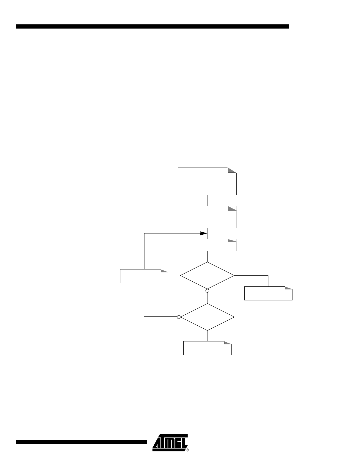
Initialization Procedure for DC/DC A converter
The initialization procedure is described in flow chart:
• Select the CVCC1 level by means of bits VCARD1[1:0] in SC1_CFG0 register,
• Set bits DEMBOOST A[1:0] in SC1_CFG4 register following the current level control wanted.
• Monitor VCARD_OK1 bit in SC1_STATUS register in order to know when the DC/DC A
Converter is ready (CVCC1 voltage has reached the expected level)
While VCC1 remains hi gher t han 3.6V an d star tup cur rent lowe r than 30 mA (dependi ng on th e
load type), the DC/DC A converter should be ready without having to increment DEMBOOSTA[1:0] bits beyond [0:0] level. If at least one of th e two conditions ar e not met (VCC <
3.6V or startup current > 30 mA), it will be necessary to increment the DEMBOOSTA[1:0] bits
until the DC/DC converter is ready.
Increment of DEMBOOSTA[1:0] bits increases at the same time the current overflow level in the
same proportion as the startup current. So once the DC/DC converter is ready it advised to decrement the DEMBOOSTA[1:0] bits to restore the overflow current to its normal or desired value.
20
7511B–SCR–10/05
Page 21
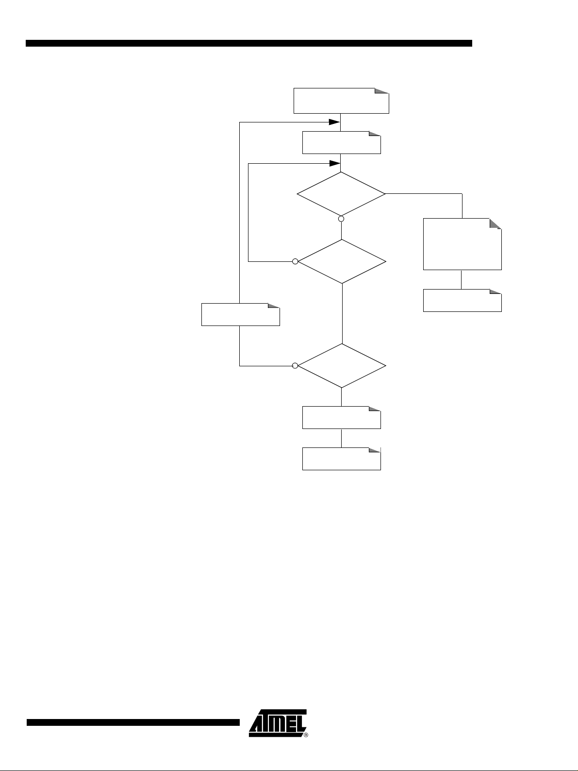
Figure 9. DC/DC A Converter Initialization Procedure
DEMBOOSTA[1:0]=[0:0]
Set Time-out to 3 ms
VCARD_OK1=1
Time-out
Expired
Increment
DEMBOOSTA[1:0]
AT83C26
Decrement
DEMBOOSTA[1:0]
to adjust the
current overflow
END
DC/DC B converter
DEMBOOSTA[1:0]
is at Maximum?
DC/DC A Converter
Initialization Failure
END
The DC/DC B converter is controlled by DCDCB register.
The DC/DC B converter can be switched on even if CPRES2 pin remains inactive.
A write operation in VDCB[1:0] (0x01, 0x02, 0x03) starts the DC/DC. When the output voltage
remains within the voltage range specified by VDCB_OK[1:0], the VDCB_OK bit is set.
The DC/DC B Converter can work in two different modes which are selected by STEPREGB:
• Pump Mode (STEPREGB = 0): an external inductance of 10 µH must be connected
between pins LIB and VCC. VCC can be higher or lower than selected voltage.
• Regulator mode (STEPREGB = 1): no external inductance is required but VCC must be
always higher than selected voltage+0.3V.
7511B–SCR–10/05
The current drawn from power suppl y by the DC/DC B conv erter is controll ed during the startup
phase in order to avoid high transient cur rent mainly in Pump Mod e which could cause the
power supply voltage to drop dramatically . This control is done by means of bits DEMBOOSTB[1:0], which increases progressively the startup current level.
21
Page 22
AT83C26
The DC/DCB sensitivity to any overflow current can be modified (20%) by using the ICCADJB bit
(DC/DCB register).
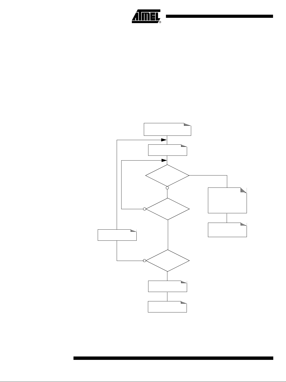
Initialization Procedure for DC/DC B converter
The initialization procedure is described in flow chart:
• Select the DC/DC B level by means of bits VDCB[1:0] in DCDCB register,
• Set bits DEMBOOSTB[1:0] in INTERFACEB register following the current level control
wanted.
• Monitor VDCB_OK bit in DCDCB register in order to know when the DC/DC B Converter is
ready
Figure 10. DC/DC B Converter Initialization Procedure
DEMBOOSTB[1:0]=[0:0]
Set Time-out to 3 ms
VDCB_OK=1
Decrement
DEMBOOSTB[1:0]
Time-out
Expired
Increment
DEMBOOSTB[1:0]
DEMBOOSTB[1:0]
is at Maximum?
DC/DC B Converter
Initialization Failure
END
to adjust the
current overflow
END
(ready to start LDO)
Increment of DEMBOOSTB[1:0] bits increases at the same time the current overflow level in the
same proportion as the startup current. So once the DC/DC B con verter is ready it advise d to
decrement the DEMBOO STB[1:0] bits to restore the overfl ow current to its nor mal or desire d
value.
22
7511B–SCR–10/05
Page 23
LDO initialization
Procedure
AT83C26
When the DC/DC B voltage rises the selected voltage (VDCB_OK=1), the card voltage selection
on CVCC2, CVCC3, CVCC4 or CVCC5 starts the corresponding LDO.
The CVCC2 card voltage must be st arted i n first (if nee ded). When the VC ARD_OK2 is set, the
CVCC3,CVCC4, CVCC5 card voltage are started one after each other (if needed) with the same
procedure.
The SC2_FULL bit must be set to use SC2 full interface:
CIO3/CC42 is CC42 and CRST3/CC82 is CC82.
As the power supply of CIO3/CC42 and of CRST3/CC8 2 is CVCC3, when SC2_FULL=1,
CVCC3 = CVCC2. The SC3 interface is disable and LDO3 receives LDO2 command
(VCARD3[1:0] = VCARD2[1:0]).
Figure 11. LDOn Initialization Procedure (n = 2, 3, 4, 5)
Init condition:
DCDCB started
(VDCB_OK = 1)
Start LDOn,
write VCARDn[1:0]
Set Timer 2ms
IPLUSn = 1
VCARD_OKn = 1
LDOn started
Time-out Expired
and IPLUSn=1
?
LDOn initialization
failure
The LDOn output voltage must be at 0V before to program 1.8V/3V/5V.
7511B–SCR–10/05
23
Page 24

AT83C26
Activation Sequence Overview (n=1, 2, 3, 4, 5)
The activation sequence on SC1 is only available if a card is detected on CPRES1 (CARDIN1 bit
= 1).
The activation sequence on SC2 is only available if a card is detected on CPRES2 (CARDIN2 bit
= 1).
The activation seq uence on SC3 , SC4, S C5, is only av ailab le if DC/DC B is s tarte d (VDCB_ OK
= 1).
The SCn interface starts the activation sequence after a TWI write command in VCARDn[1:0]
bits to program the CVCCn voltage.
The SC3, SC4, SC5 interfaces (SIM/SAM interfaces) don’t have card presence detector.
After the DC/DC start, the user ap plicati on will check the AT R to detect if a SIM/SAM is present
in the connector.
The automatic reset transition mode (ART=1) controls the CRST pin and check if the first start
bit of the ATR respects ISO7816 timings.
All status bits of an interface (see bits in registers with ”This bit is cleared by hardware when this
register is read”) must be cleared before to start an activation sequence.
Software Activation for SCn interfaces (n=1, 2, 3, 4, 5) with ARTn bit = 0
The activation sequence is controlled by s oftware using TWI co mmands, depend ing on the
cards to support. For ISO 7816 cards, the following sequence can be applied:
1. Card Voltage is set by software to the required value (VCARDn[1:0] bits). The TWI
writing command in VCARDn[1:0] starts the DC/DC (or LDO).
2. Wait of the end of the DC/DC (or LDO) init with a polling on VCARD_OKn bit or wait
for INT
be set by software.
3. CKSTOPn, IODISn are programmed by software. CKSTOPn bit is reset to have the
clock running. IODISn (see IO_SELECT for SC2, SC3, SC4, SC5) is reset to enable
the transparent mode on CIOn,CC4n, CC8n.
4. CRSTn pin is controlled by software using CARDRSTn bit.
to go Low. When VCARD_OKn bit is set (by hardware), CARDIOn bit should
24
7511B–SCR–10/05
Page 25

Figure 14. Software activation without auto mat ic contr ol (ARTn bit = 0)
AT83C26
CVCCn
CRSTn
CCLKn
CIOn
1
3
4
ATR
2
Note:
– It is assumed that initially VCARDn[1:0], CARDCKn, CARDIOn and CARDRSTn bits
are cleared, CKSTOPn and IODISn are set (those bits are further explained in the
registers description)
– The user should check the AT83C26 status and possibly resume the activation
sequence if one TWI transfer is not acknowledged during the activation sequence.
Software activation for SCn (n=1, 2, 3, 4, 5) interfaces and ARTn bit = 1
The following sequence can be applied:
1. Card Voltage is set by software to the required value (VCARDn1:0] bits in
SCn_CFG0 register). This writing starts the DC/DC converter (or LDO).
2. Wait of the end of the DC/DC init (or LDO) with a polling on VCARD_OKn bit or wait
for INT
to go Low. When VCARD_OKn bit is set (by hardware), CARDIOn bit should
be set by software.
3. CKSTOPn, IODISn are programmed by software. CKSTOPn bit is reset to have the
clock running. IODISn is reset to enable the transparent mode on CIOn,CC4n,
CC8n.
4. CARDRSTn bit is set by software.
Automatic Reset Transition description:
A 16-bit counter sta rts w hen CARDR STn b it is set. It cou nts ca rd cl ock cy cles. T he CRS Tn signal is set when the counter reaches the TIMER_MSB and TIMER_LSB value which corresponds
to the “tb” time (Figure 15).The counter is reseted when the CRSTn pin is released and it is
stopped at the first start bit of the Answer To Request (ATR) on CIOn pin.
The CIOn pin is not ch ecked dur ing the firs t 200 clo ck cycles (t a, Figure 15). If the ATR arrives
before the counter reaches TIMER_MSB and TIMER_LSB values, the activation sequence fails,
7511B–SCR–10/05
25
Page 26

AT83C26
the CRSTn signal is not set and th e CAP T URE_ MS B and CAP T URE _LSB r egi st er s conta in the
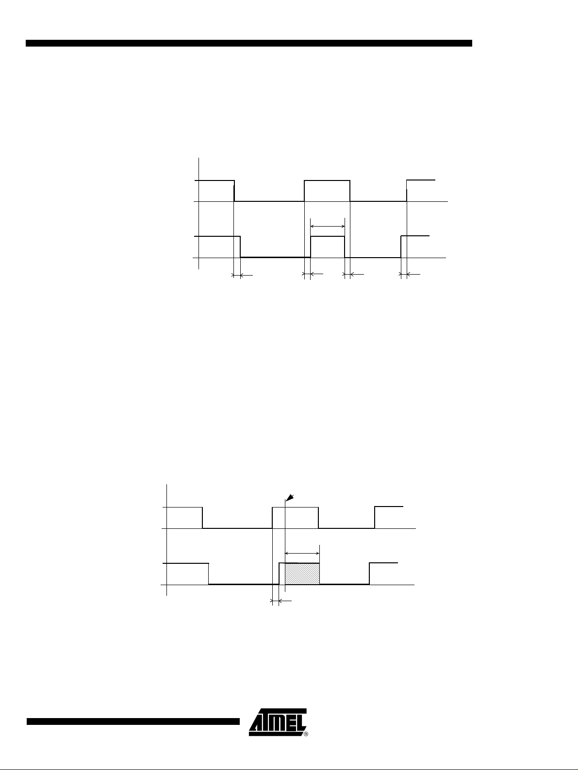
value of the counter at the arrival of the ATR.
If the ATR arrives after the rising edge on CRSTn pin and before the card clock counter overflows (65535 clock cycles), the activation sequence completes. The CAPTURE_MSB and
CAPTURE_LSB registers contain the value of the counter at the arrival of the ATR (tc time on
Figure 15).
Figure 15. Software activation with ARTn bit = 1
CARDRSTn bit set
CVCCn
4
3
1
CRSTn
CCLKn
CIOn
ta
2
tb
ISO 7816 constraints: ta = 200 card clock cycles
400 card clock cycles< = tb
tc
Warm reset (n=1, 2, 3, 4, 5)
26
400 card clock cycles< = tc < = 40000 card clock cycles
Timer[1-0] reset value is 400.
The AT83C26 offers a simple and accurate way to control the CRSTn signal during a warm
reset.
After an activation sequenc e (cold reset), a warm r eset is st arted wi th a low level on CRST during a define delay (between 40000 and 45000 clock cycles for example).
The ARTn bit, the TIMER_MSB and the TIMER_LSB are used to control CRSTn.
The first step is to load the number of CCLK cycles with CRSTn=0 in TIMER registers.
The warm reset is started by setting ART bit (if ART bit is already set, reset ART before).
7511B–SCR–10/05
Page 27

AT83C26
The CRST signal will be equal to 0 during the number of clock cycles programmed in
TIMER_MSB and TIMER_LSB. Then, the CRST signal will be at 1.
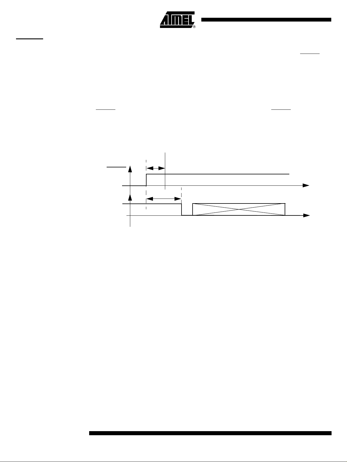
Figure 16. Warm reset with ARTn bit = 1
ART = 1
CVCCn
CRSTn
CCLKn
CIOn
Deactivation Sequence Overview
The deactivation sequence should follows the order defined in ISO7816-3 specification. The
AT83C26 has two deactivation modes:
• Standard deactivation mode: This mode is used to stop exchange with smart card when the
AT83C26 power supply is present. The DCCLK signal is used for deactivation sequence
timings.
• Emergency deactivation mode: This mode is used when the AT83C26 power supply is took
off.
Deactivation sequence on SCn interface (n=1, 2, 3, 4, 5)
The card automatic deactivation is triggered when one the following condition occurs:
• ICARDERR1 bit is set by hardware (SC1)
• VCARDERRn bit is set by hardware (or by software)
• INSERT1 is set and CARDIN1 is cleared (SC1)
• INSERT2 is set and CARDIN2 is cleared (SC2)
• SHUTDOWNA bit is set by software (SC1)
• SHUTDOWNB bit is set by software (SC2, SC3, SC4, SC5)
t
t = TIMER value
7511B–SCR–10/05
27
Page 28

AT83C26
• Reset pin going low (SC1, SC2, SC3, SC4, SC5)
•Power Fail (VPFDP)
It is a self-timed sequence whi ch can not be inter rup ted whe n sta rt ed ( see F i gure 17) . Each ste p
is separated by a delay based on Td equal to 8 periods of DCCLK, typically 2 to 2.4 µs:
1. T0: CARDRSTn is cleared, SHUTDOWNA (for SC1) bit is set.
2. T0 + 5 x Td:CARDCKn is cleared, CKSTOPn, CARDIOn and IODIS are set.
3. T0 + 6 x Td: CARDIOn is cleared.
4. T0 + 7 x Td: VCARDn[1:0] = 00.
Figure 17. Deactivation Sequence
CVCC
CRST
CCLK
CIO,
CC4,
CC8
5 x Td
t1
Notes: 1. Setting ICARDERR1 by software does not trigger a deactivation on SC1. VCARDERRn can
be used to deactivate the card by software.
2. If CCLKn=A2 or A2/2, deactivation follows fig13 with 2 timing modifications: t1=5.5*Td and
t2=0.5*Td.
3. Td is based on DCCLK clock.
Emergency deactivation sequence on SCn interface (n=1, 2, 3, 4, 5)
The card emergency automatic deactivation is triggered when one the following condition
occurs:
• Software TWI Reset (SC1, SC2, SC3, SC4, SC5)
• Power fail on VCC (SC1, SC2, SC3, SC4, SC5)
If the power supply is disconnected, a standard deactivation is started when VCC = VPFDP.
When VCC is equal to VPFDM, the emergency deactivation occurs and eventually ends the
standard deactivation.
Td
t2
Td
28
7511B–SCR–10/05
Page 29

Figure 18. Power Fail Detection
VCC
start standard deactivation
VPFDP
VPFDM
start emergency deactivation
Figure 19. Emergency deactivation sequence
CVCC
CRST
AT83C26
CCLK
CIO,
CC4,
CC8
During an emergency deactivation, the signals fall according to the order described in Fig18.
Transparent mode
Full transparent mode on SCn interfaces (n=1, 2)
If the micro controller outputs ISO 7816 signals, a transparent mode allows to connect, CCLK,
CIO, CRST, CC4 and CC8 signals on outputs after an electrical level control. The AT83C26
level shifters adapt the card signals to the smart card voltage selection.
The CCLK micro controller signal can be connected to the A2/CK pins (see CKSn[2:0]).
CKSn[2:0] bits allow to select standard or transparent configuration for the CCLKn pin. A2/CK
inputs always give the TWI address at reset.
If A2/CK input is tied to the host micro controller and its reset value is unknown, a general call on
the TWI bus allows to re set all the AT83C26 devices and set its add ress after A2/ CK input is
fixed.
7511B–SCR–10/05
29
Page 30

AT83C26
Figure 20. Transparent Mode Description
Micro controller
AT83C26
CCLK
CRST
CIO
CC4
CC8
Full transparent mode on SCn interfaces (n= 3, 4, 5)
The transparent mode wi th A2/CK is also ava ilable for SC3, SC4 an d SC5 interfaces without
CC4 and CC8.
Figure 21. Transparent Mode Description
Micro controller
CCLK
A2/CK
A1/RST
I/O1
AUX1
AUX2
A2/CK
AT83C26
CCLKn
CRSTn
CIOn
CC4n
CC8n
CCLKn
SMART CARD
Interrupts
CIO
I/O2
CRSTn
CIOn
SIM/SAM
The INT output is High by default. INT is driven Low by at least one of the following event:
– INSERT1 or INSERT2 bits set (card insertion/extraction or bit set by software)
– VCARD_INTn (n=1,2,3,4,5) bits set (the DC/DC A or LDO2 to LDO5 output voltage
has settled)
– VDCB_INT bit set (the DC/DC B output voltage has settled)
– over-current detection on CVCC1
– VCARDERRn bit set (out of range voltage on CVCCn or bit set by software)
(n=1,2,3,4,5)
– ATRERRn bit set (no ATR before the card clock counter overflows or bit set by
software) (n=1,2,3,4,5)
30
7511B–SCR–10/05
Page 31

AT83C26
Several AT83C26 devices can share the same interrupt pin and the micro controller can identify
the interrupt sources by polling the interrupt bits of the AT83C26 devices using TWI commands.
A TWI read command of the int errupt bi t corres ponding to the IT clears the bit. W hen all IT bits
are cleared, the INT
The ITDIS register contains 4 bits to control SCn interrupts (n= 2,3,4,5). If ITDISn bit is set, the
flags are set but the INT
Table 4. Interr upt bits des crip tio n
output becomes high.
pin isn’t driven low if an interrupt event appears.
Bit name Register name Mask on
INT pin
INSERT1
INSERT2
VCARD_INT1
VCARD_INT2
VCARD_INT3
VCARD_INT4
VCARD_INT5
VDCB_INT
ICARDERR1
VCARDERR1
VCARDERR2
VCARDERR3
VCARDERR4
VCARDERR5
ATRERR1
SC1_CFG0
SC2_CFG0
SC1_STATUS
SC2_CFG0
SC3_CFG0
SC4_CFG0
SC5_CFG0
DCDCB
SC1_CFG0
SC1_CFG0
SC2_CFG0
SC3_CFG0
SC4_CFG0
SC5_CFG0
SC1_CFG0
ITDIS2
ITDIS2
ITDIS3
ITDIS4
ITDIS5
ITDIS2
ITDIS3
ITDIS4
ITDIS5
Remark
Smart card inserted/extracted in SC1
Smart card inserted/extracted in SC2
VCARD_OK1 is set
VCARD_OK2 is set
VCARD_OK3 is set
VCARD_OK4 is set
VCARD_OK5 is set
VDCB_OK is set
Over current on DCDCA.
Ouput voltage out of range on DCDCA
Ouput voltage out of range on LDO2
Ouput voltage out of range on LDO3.
Ouput voltage out of range on LDO4
Ouput voltage out of range on LDO5
Error on SC1 for ATR reception in automatic mode
ATRERR2
ATRERR3
ATRERR4
ATRERR5
7511B–SCR–10/05
SC2_CFG0
SC3_CFG0
SC4_CFG0
SC5_CFG0
ITDIS2
ITDIS3
ITDIS4
ITDIS5
Error on SC2 for ATR reception in automatic mode
Error on SC3 for ATR reception in automatic mode
Error on SC4 for ATR reception in automatic mode
Error on SC5 for ATR reception in automatic mode
31
Page 32

AT83C26
After the reading and the clear of the interrupt bits, several bits are used to control the status.
Table 5. Status bits description
Bit name Register name Remark
CARDIN1
CARDIN2
VCARD_OK1
VCARD_OK2
VCARD_OK3
VCARD_OK4
VCARD_OK5
VDCB_OK
Slew rate control
SC1_STATUS
SC1_STATUS
SC1_STATUS
SC2_CFG0
SC3_CFG0
SC4_CFG0
SC5_CFG0
DCDCB
The status for the ICARDERR1 and VCARDERRn (n= 1 to 5) bits is controlled with
VCARD_OKn bits.
The status for the ATRERRn (n= 1 to 5) is controlled by reading of values in CAPTURE_MSB
and CAPTURE_LSB.
The AT83C26 proposed a slew rate co ntr ol on CIOn and CCLKn pin s (n= 1, 2, 3, 4, 5). T he c ontrol operates on rising and falling edges of CCLKn and only on rising edge of CIOn.
Smart card presence in SC1
Smart card presence in SC2
CVCC1 voltage in range programmed in VCARD1[1:0]
CVCC2 voltage in range programmed in VCARD2[1:0]
CVCC3 voltage in range programmed in VCARD3[1:0]
CVCC4 voltage in range programmed in VCARD4[1:0]
CVCC5 voltage in range programmed in VCARD5[1:0]
CVCCB voltage in range programmed in VDCB[1:0]
Power down mode
32
Four modes are available:
• Automatic mode: The slew rate depends on VCARDn[1:0] value. The slew rate value is
optimized according to CVCCn.
• Mode 1, 2 , 3 (1.8V, 3V, 5V): The user can forced the slew rate if needed. For example if
CVCCn = 5V, the user can program 1.8V or 3V to speed up the slew rate in case of long wire
connection between AT83C26 and smart cards.
SHUTDOWNA bit and SHUTDOWN B bit m ust be s et to a ctivate power do wn mode on DCDCA
and DCDCB converters.
If SHUTDOWNA = SHUTDOWNB = 1, the AT83C26 internal regulator also enters in power
down mode. The consumption is then about 30µA.
To exit from power down mode, TWI commands are needed to clear SHUTDOWNA and
SHUTDOWNB.
7511B–SCR–10/05
Page 33

Write Commands
AT83C26
The write commands are:
1. General Call Reset:
A general call followed by the value 06h has the same effect as a Reset command.
2. Reset:
Initialize all the logic and the TWI interface as after a power-up or power-fail reset. If the
interface i s activat ed, a n emerge ncy de -activat ion seq uence is also per formed. This is a
one-byte command.
3. Write SC1_CFG0, SC1_CFG1, SC1_CFG2, SC1_CFG3, SC1_CFG4:
Configure the dev ice acco rding to the last six bits in th e SC1_ CFG0 reg ister and to the fo l-
lowing four bytes in SC1_CFG1, SC1_CFG2, SC1_CFG3 then SC1_CFG4 registers. This is
a five bytes command.
Figure 22. Command byte format for Write SC1_CFG0 command
b7
b6
0
1
b4
b5
X
XX
SC1_CFG0 on 6 Bits
b3
b2 b1
X
b0
X
X
4. Write TIMER_MSB, TIMER_LSB:
Program the 16-bit automatic re set transitio n timer with the fo llowing two bytes. This is a
three bytes command.
5. Wri te SC1_INTERFACE:
Program the interface by te. This is a one-b yte co mmand. The MSB of the comman d byte is
fixed at 0.
6. Write common config smart cards:
IO_SELECT, INTERFACE_B, ITDIS:
Configuration of parameters for smart card interfaces.
7. Write SC2 interface: SC2_CFG0, SC2_CFG1, SC2_CFG2
Configuration of smart card interface 2.
7511B–SCR–10/05
8. Write SC3 interface: SC3_CFG0, SC3_CFG2
Configuration of SIM/SAM interface 3.
9. Write SC4 interface: SC4_CFG0, SC4_CFG2
Configuration of SIM/SAM interface 4.
33
Page 34

AT83C26
10. Write SC5 interface: SC5_CFG0, SC5_CFG2
Configuration of SIM/SAM interface 5.
11. Write DCDCB config: DCDCB, LDO
Configuration of DCDCB converter.
12. Write SLEW_CTRL config: SLEW_CTRL_1, SLEW_CTRL_2, SLEW_CTRL_3
Configuration of slew rate for CCLKn and CIOn (n = 1, 2, 3, 4, 5).
Table 6. Write Commands Description
Address
Byte
(See Table 2) Command Byte Data Byte 1 Data Byte 2 Data Byte 3 Data Byte 4
[0] [1] [2] [3] [4]
1. General Call Res e t 0000 0000 0000 0110
2. Reset 0100 XX10 1111 1111
3. Write config 0100 XX10 (10 + SC1_CFG0 6 bits) SC1_CFG1 SC1_CFG2 SC1_CFG3 SC1_CFG4
4. Write Timer 0100 XX10 1111 1100 TIMER_MSB TIMER_LSB
5. Write Interface 0100 XX10 (0+SC1_INTERFACE 7 bits)
6.Write Config SC on DCDCB 0100 XX10 1111 1000 IO_SELECT INTERFACE_B ITDIS
7. Write SC2 interface 0100 XX10 1111 1001 SC2_CFG0 SC2_CFG1 SC2_CF G2
8. Write SC3 interface 0100 XX10 1111 1010 SC3_CFG0 SC3_CFG2
9. Write SC4 interface 0100 XX10 1111 1011 SC4_CFG0 SC4_CFG2
10. Write SC5 interface 0100 XX10 1111 1101 SC5_CFG0 SC5_CFG2
11. Wri te DCDCB config 0100 XX10 1111 1110 DCDCB LD O
12. Write SLEW_CTRL config 0100 XX10 1111 0111 SLEW_CTRL_1 SLEW_CTRL_2 SLEW_CTRL_3
34
7511B–SCR–10/05
Page 35

Read Command
AT83C26
After a write command, even with a length of 0 byte, the next read operation is performed on the
corresponding byte. The write command sets the “read pointer”.
After the reset, the “read pointer” is on SC1 registers
FFh is completing the transfer if the micro controller attempts to read beyond the last byte.
Flags are only reseted after the corresponding byte read has been acknowledged by the master.
Figure 23. Read command byte
b7 b6 b5 b4 b3 b2 b1
1
0
0
0
X
X
A2 A1
levels on reset
b0
1
1
Table 7. Read Commands Description
1. After reset or
write command
number 2, 3, 4
[0] SC1_STATUS STATUSB SC2_CFG0 SC3_CFG0 SC4_CFG0 SC5_CFG0 DCDCB SLEW_CTRL_1
[1] SC1_CFG0 IO_SELECT SC2_CFG1 SC3_CFG2 SC4_CFG2 SC5_CFG2 LDO SLEW_CTRL_2
[2] SC1_CFG1 INTERFACE_B SC2_CFG2 0xFF 0xFF 0xFF 0xFF SLEW_CTRL_3
[3] SC1_CFG2 ITDIS 0xFF 0xFF 0xFF 0xFF 0xFF 0xFF
[4] SC1_CFG3 0xFF 0x FF 0xFF 0xFF 0x FF 0xFF 0xFF
[5] SC1_CFG4 0xFF 0x FF 0xFF 0xFF 0x FF 0xFF 0xFF
[6] SC1_INTERFACE 0xFF 0xFF 0xFF 0xFF 0xFF 0xFF 0xFF
2. After
write
command
number 6
3. After
write command
number 7
4. After
write
command
number 8
5. After
write
command
number 9
6. After
write
command
number 10
7. After
write
command
number 11
8. After
write
command
number 12
[7] TIMER_MSB 0xFF 0xFF 0xFF 0xFF 0xFF 0xFF 0xFF
[8] TIMER_LSB 0xFF 0xFF 0xFF 0xFF 0xFF 0xFF 0xFF
[9] CAPTURE_MSB 0xFF 0xFF 0xFF 0xFF 0xFF 0xFF 0xFF
[10] CAPTURE_LSB 0xFF 0xFF 0xFF 0xFF 0xFF 0xFF 0xFF
[11] 0x FF 0xFF 0xFF 0xFF 0xFF 0xFF 0xFF 0xFF
7511B–SCR–10/05
35
Page 36

AT83C26
Registers summary
The table below gives a quick view on AT83C26 registers.
Table 8. Smart card 1 interface registers
7 6 5 4 3 2 1 0
SC1_CFG0
SC1_CFG1
SC1_CFG2
SC1_CFG3
SC1_CFG4
SC1_INTERFACE
SC1_STATUS
SC2_CFG0
SC2_CFG1
SC2_CFG2
SC3_CFG0
1 0 ATRERR1 INSERT1 ICARDERR1 VCARDERR1 VCARD11 VCARD10
X ART1 SHUTDOWNA CARDDET1 PULLUP1 CDS12 CDS11 CDS10
0 DCK2 DCK1 DCK0 X CKS12 CKS11 CKS10
X X X ICCADJA X X X X
X DEMBOOSTA1 DEMBOOSTA0 STEPREGA INT_PULLUP X X CRST_SEL1
0
CC81 CC41 CARDIN1 VCARD_OK1 X VCARD_INT1 CRST1 CIO1
IODIS1
CKSTOP1 CARDRST1 CARDC81 CARDC41 CARDCK1 CARDIO1
Table 9. Smart card 2 interface registers
7 6 5 4 3 2 1 0
VCARD_INT2 VCARD_OK2 ATRERR2 INSERT2 X VCARDERR2 VCARD21 VCARD20
X X SC2_FULL CARDDET2 PULLUP2 CDS22 CDS21 CDS20
ART2 CRST_SEL2 CARDRST2 CARDCK2 CKSTOP2 CKS22 CKS21 CKS20
Table 10. SIM/SAM 3 interface registers
7 6 5 4 3 2 1 0
VCARD_INT3 VCARD_OK3 ATRERR3 X X VCARDERR3 VCARD31 VCARD30
SC3_CFG2
SC4_CFG0
SC4_CFG2
SC5_CFG0
SC5_CFG2
36
ART3 X CARDRST3 CARDCK3 CKSTOP3 CK32 CKS31 CKS30
Table 11. SIM/SAM 4 interface registers
7 6 5 4 3 2 1 0
VCARD_INT4 VCARD_OK4 ATRERR4 X X VCARDERR4 VCARD41 VCARD40
ART4 X CARDRST4 CARDCK4 CKSTOP4 CKS42 CKS41 CKS40
Table 12. SIM/SAM 5 interface registers
7 6 5 4 3 2 1 0
VCARD_INT5 VCARD_OK5 ATRERR5 X X VCARDERR5 VCARD51 VCARD50
ART5 X CARDRST5 CARDCK5 CKSTOP5 CKS52 CKS51 CKS50
7511B–SCR–10/05
Page 37

AT83C26
Table 13. Common registers for SC1/SC2/SC3/SC4/SC5
7 6 5 4 3 2 1 0
TIMER_MSB
TIMER_LSB
CAPTURE_MSB
CAPTURE_LSB
IO_SELECT
INTERFACEB
STATUSB
ITDIS
DCDCB
LDO
Bit 15 Bit 14 Bit 13 Bit 12 Bit 11 Bit 10 Bit 9 Bit 8
Bit 7 Bit 6 Bit 5 Bit 4 Bit 3 Bit 2 Bit 1 Bit 0
Bit 15 Bit 14 Bit 13 Bit 12 Bit 11 Bit 10 Bit 9 Bit 8
Bit 7 Bit 6 Bit 5 Bit 4 Bit 3 Bit 2 Bit 1 Bit 0
X X X X IOSEL3 IOSEL2 IOSEL1 IOSEL0
Table 14. Common registers for SC2/SC3/SC4/SC5
7 6 5 4 3 2 1 0
X CARDC82 CARDIO5 CARDIO4
X CARDIN2 CIO5 CIO4
IODIS5 IODIS4 IODIS3 IODIS2 ITDIS5 ITDIS4 ITDIS3 ITDIS2
CARDIO3/
CARDC42 CARDIO2 DEMBOOSTB1 DEMBOOSTB0
CRST3/
CC82
CIO3/
CC42 CRST2 CIO2
Table 15. DC/DC B registers
7 6 5 4 3 2 1 0
SHUTDOWNB VDCB_INT VDCB_OK 0 ICCADJB STEPREGB VDCB1
IPLUS5 IPLUS4 IPLUS3 IPLUS2 X X X X
VDCB0
SLEW_CTRL_1
SLEW_CTRL_2
SLEW_CTRL_3
Table 16. Slew control registers for CIO and CCLK pins
7 6 5 4 3 2 1 0
CCLK2_SLEW_CTRL1CCLK2_SLEW_CT
CCLK4_SLEW_CTRL1CCLK4_SLEW_CT
X X X X
RL0
RL0
CIO2_SLEW_CT
RL1
CIO4_SLEW_CT
RL1
CIO2_SLEW_CT
RL0
CIO4_SLEW_CT
RL0
CCLK1_SLEW_CT
RL1
CCLK3_SLEW_CT
RL1
CCLK5_SLEW_CT
RL1
CCLK1_SLEW_CT
RL0
CCLK3_SLEW_CT
RL0
CCLK5_SLEW_CT
RL0
CIO1_SLEW_CT
RL1
CIO3_SLEW_CT
RL1
CIO5_SLEW_CT
RL1
CIO1_SLEW_CTR
L0
CIO3_SLEW_CTR
L0
CIO5_SLEW_CTR
L0
7511B–SCR–10/05
37
Page 38

AT83C26
Registers
Table 17. SC1_ CFG0(Config Byte 0 for SC1)
7 6 5 4 3 2 1 0
1 0 ATRERR1 INSERT1 ICARDERR1 VCARDERR1 VCARD11 VCARD10
Bit Number Bit Mnemonic Description
7-6 1-0 These bits cannot be programmed and are read as 1-0.
Answer to Reset Interrupt for S C1
5 ATRERR1
4 INSERT1
3 ICARDERR1
2 VCARDERR1
This bit is set when the card clock counter overflows (no falling edge on CIO1 is received before the overflow
of the card clock counter).
This bit is cleared by hardware when this register is read. It can be set by software for test purpose.
Card Insertion Interrupt
This bit is set when a card is inserted or extracted: a change in CARDIN value filtered according to CDS[2-0].
It can be set by software for test purpose.
This bit is cleared by hardware when this register is read. It cannot be cleared by software.
Card Over Current Interrupt
This bit is set when an over current is detected on CVCC. It can be set by software for test purpose (no card
deactivation is performed).
This bit is cleared by hardware when this register is read. It cannot be cleared by software.
Card Out of Range Voltage Interrupt
This bit is set when the output voltage goes out of the voltage range specified by VCARD field. It can be set
by software for test purpose and deactivate the card.
This bit is cleared by hardware when this register is read. It cannot be cleared by software.
1-0 VCARD1[1:0]
Reset value = 0x 1000 0000
Card Voltage Selection
VCARD1[1:0] = 00: 0V
VCARD1[1:0] = 01: 1.8V
VCARD1[1:0] = 10: 3V
VCARD1[1:0] = 11: 5V
VCARD1[1:0] writing to 1.8V, 3V, 5V starts the DC/DC if a card is detected.
VCARD1[1:0] writing to 0 stops the DC/DC.
No card deactivation is performed when the voltage is changed between 1.8V, 3V or 5V. The micro controller
should deactivate the card before changing the voltage.
38
7511B–SCR–10/05
Page 39

SC1_CFG
Table 18. SC1_CFG1 (Config Byte 1 for SC1
7 6 5 4 3 2 1 0
X ART1 SHUTDOWNA CARDDET1 PULLUP1 CDS12 CDS11 CDS10
Bit Number Bit Mnemonic Description
7 X
Automatic Reset Transition
6 ART1
5
4 CARDDET1
SHUTDOWNA
Set this bit to have the CRST1 pin changed according to activation sequence.
Clear this bit to have the CRST1 pin immediately following the value programmed in CARDRST1.
Shutdown DC/DCA
Set this bit to reduce the power consumption. An automatic de-activation sequence will be done.
VCARD[1:0] bits are reset.
Clear this bit to enable VCARD1[1:0] selection.
Card Presence Detection Polarity
Set this bit to indicate the card presence detector is closed when no card is inserted (CPRES is low).
Clear this bit to indicate the card presence detector is open when no card is inserted (CPRES is high).
AT83C26
3 PULLUP1
2-0 CDS1[2:0]
Reset value = 0x X000 1010
Pull-up Enable
Set this bit to enable the internal pull-up on the CPRES pin. This allows to minimize the number of external
components.
Clear this bit to disable the internal pull-up and minimize the power consumption when the card detection
contact is on. Then an external pull-up must be connected to V
Card Detection filtering
CPRES1 is sampled by the master clock provided on CLK input. A change on CPRES1 is detected after:
CDS1[2-0] = 0: no sample
CDS1[2-0] = 1: 4 identical samples
CDS1[2-0] = 2: 8 identical samples (reset value)
CDS1[2-0] = 3: 16 identical samples
CDS1[2-0] = 4: 32 identical samples
CDS1[2-0] = 5: 64 identical samples
CDS1[2-0] = 6: 128 identical samples
CDS1[2-0] = 7: 256 identical samples
Note: 1. When CDS[2-0] = 0, a card insertion (even if CLK is stopped) puts a low level on INT pin. This
can be used to wake up the external micr o controller and restart CLK w hen a card is inser ted
in the AT83C24.
(1)
(typically a 1 MΩ resistor).
CC
7511B–SCR–10/05
39
Page 40

AT83C26
Table 19. SC1_CFG2 (Config Byte 2 for SC1)
7 6 5 4 3 2 1 0
0 DCK2 DCK1 DCK0 X CKS12 CKS11 CKS10
Bit Number Bit Mnemonic Description
7 0 This bit must be always at 0.
DCK is the first level of prescaler factor. CLK signal is divided by the prescaler value and outputs DCCLK
signal. DCCLK is an input for CCLK prescaler.
DCK[2:0] = 0: prescaler factor equals 1
DCK[2:0] = 1: prescaler factor equals 2
DCK[2:0] = 2: pr escaler factor equals 4
6-4 DCK[2:0]
3 X
2-0 CKS1[2:0]
DCK[2:0] = 3: prescaler factor equals 6
DCK[2:0] = 4: prescaler factor equals 8
DCK[2:0] = 5: prescaler factor equals 10
DCK[2:0] = 6: prescaler factor equals 12
DCK[2:0] = 7: Reserved
DCCLK is used for pad management and dectivation sequence.
Card Clock prescaler factor for CCLK1.
CKS1 [2:0] = 0: CCLK1 = CLK (the maximum frequency on CLK is 24 MHz)
CKS1 [2:0] = 1: CCLK1 = DCCLK
CKS1[2:0] = 2: CCLK1 = DCCLK / 2
CKS1[2:0] = 3: CCLK1 = DCCLK / 4
CKS 1[2:0] = 4: CCLK1 = A2
CKS1 [2:0] = 5: CCLK1 = A2 / 2
CKS1[2:0] = 6: CCLK1 = CLK / 2
CKS1 [2:0] = 7: CCLK1 = CLK / 4
40
Reset value = 0x 0001 X000
Notes: 1. When CKS1 value is changed a special logic insures no glitch occurs on the CCLK1 pin and
actual configuration changes can be delayed by half a period to two periods of CCLK1.
2. CCLK1 must be stopped with CKSTOP1 bit before switching from CKS1 = (0, 1, 2, 3, 6, 7) to
CKS1 = (4, 5) or vice versa.
7511B–SCR–10/05
Page 41

Table 20. SC1_CFG3 (Config Byte 3 for SC1)
7 6 5 4 3 2 1 0
X X X ICCADJA X X X X
Bit Number Bit Mnemonic Description
7-5 X
CICC overflow adjust
This bit controls the DC/DCA sensitivity to any overflow current.
4 ICCADJA
3 X
2 X
1 X
0 X
Set this bit to decrease the DC/DCA sensitivity (CI
Clear this bit to have a normal configuration.
The reset value is 0.
is increased by about 20%).
CC_ovf
Reset value = 0x XXX0 XXXX
AT83C26
7511B–SCR–10/05
41
Page 42

AT83C26
Table 21. SC1_CFG4 (Config Byte 4 for SC1)
7 6 5 4 3 2 1 0
X DEMBOOSTA1 DEMBOOSTA0 STEPREGA INT_PULLUP X X CRST_SEL1
Bit Number Bit Mnemonic Description
7 X
DC/DC A Maximum Startup Current drawn from power supply
00: Normal: 80 mA average
6-5 DEMBOOSTA[1-0]
4 STEPREGA
3 INT_PULLUP
2 X
01: Normal + 18%
10: Normal + 18% (and boost on oscillator)
11: Normal + 40%
Step Regulator mode
Clear this bit to enable the automatic step-up converter (CVCC is stable even if VCC is not
higher than CVCC).
Set this bit to permanently disable the step-up co nvert er (CVCC is stable only if VCC is
sufficiently higher than CVCC).
This bit must always be set if no external self is used
Internal pull-up
Set this bit to activate the internal pull-up (connected internally to VCC) on INT pin.
Clear this bit to deactivate the internal pull-up.
1 X
0 CRST_SEL1
Reset value = 0x X000 0000
Card Reset Selection
Set this bit to have the CRST1 pin driven by hardware through the A1/RST pin.
Clear this bit to have the CRST1 pin driven by software through the CARDRST bit.
The reset value is 0.
42
7511B–SCR–10/05
Page 43

AT83C26
_
Table 22. SC1_INTERFACE (Interface Byte for SC1)
7 6 5 4 3 2 1 0
0 IODIS1 CKSTOP1 CARDRST1 CARDC81 CARDC41 CARDCK1 CARDIO1
Bit Number Bit Mnemonic Description
7 0 This bit should not be set.
Card I/O isolation
6 IODIS1
5 CKSTOP1
4 CARDRST1
Set this bit to drive the CIO1, CC41, CC81 pins according to CARDIO1, CARDC41, CARDC81
respectively.
Clear this bit to drive the CIO1, CC41 and CC81 pins connected to inputs according to IOSEL[3/0] bits.
CARD Clock Stop
Set this bit to stop CCLK1 according to CARDCK1. This can be used to set asynchronous cards in powerdown mode (GSM) or to drive CCLK1 by software.
Clear this bit to have CCLK1 running according to CKS1. This can be used to activate asynchronous cards.
Note: When this bit is changed a special logic ensures that no glitch occurs on the CCLK1 pin and
actual configuration changes can be delayed by half a period to two periods of CCLK1.
Card Reset
Set this bit to enter a reset sequence according to ART1 bit value.
Clear this bit to drive a low level on the CRST1 pin.
3 CARDC81
2 CARDC41
1 CARDCK1
0 CARDIO1
Reset value = 0x 0110 0000
Card C8
Set this bit to drive the CC81 pin High with the on-chip pull-up (according to IODIS1 bit value). The pin can
then be an input (read in SC1_STATUS register).
Clear this bit to drive a low level on the CC81 pin (according to IODIS1 bit value).
Card C4
Set this bit to drive the CC41 pin High with the on-chip pull-up (according to IODIS1 bit value). The pin can
then be an input (read in SC1_STATUS register).
Clear this bit to drive a low level on the CC41 pin (according to IODIS1 bit value).
Card Clock
Set this bit to set a high level on the CCLK1 pin (according to CKSTOP1 bit value).
Clear this bit to drive a low level on the CCLK1 pin.
Card I/O
Set this bit to drive the CIO1 pin High with the on-chip pull-up (according to IODIS1 bit value). The pin can
then be an input (read in SC1_STATUS register).
Clear this bit to drive a low level on the CIO1 pin (according to IODIS1 bit value).
7511B–SCR–10/05
43
Page 44

AT83C26
Table 23. SC1_ STAT US (Statu s By te for SC1)
7 6 5 4 3 2 1 0
CC81 CC41 CARDIN1 VCARD_OK1 X VCARD_INT1 CRST1 CIO1
Bit Number Bit Mnemonic Description
7 CC81
6 CC41
5 CARDIN1
4 VCARD_OK1
3 X
2 VCARD_INT1
1 CRST1
0 CIO1
Reset value = reset value depends on hardware configuration
Card CC8
This bit provides the actual level on the CC8 pin when read.
Card CC4
This bit provides the actual level on the CC4 pin when read.
Card Presence Status
This bit is set when a card is detected.
It is cleared otherwise.
SC1 Voltage Status
This bit is set by the DCDCA when the output voltage remains within the voltage range specified by
VCARD1[1:0] bits.
It is cleared otherwise.
SC1 Smart Card voltage interrupt
This bit is set when VCARD_OK1 bit is set.
This bit is cleared when read by the micro controller.
Card RST
This bit provides the actual level on the CRST pin when read.
Card I/O
This bit provides the actual level on the CIO pin when read.
44
7511B–SCR–10/05
Page 45

Table 24. SC2_CFG0 ()
7 6 5 4 3 2 1 0
AT83C26
VCARD_INT2VCARD_OK
2
Bit Number Bit Mnemonic Description
7 VCARD_INT2
6 VCARD_OK2
5 ATRERR2
4 INSERT2
3 X
2 VCARDERR2
ATRERR2 INSERT2 X VCARDERR2 VCARD21 VCARD20
SC2 voltage interrupt
This bit is set when VCARD_OK2 bit is set.
This bit is cleared when read by the micro controller.
SC2 Voltage Status
This bit is set by the LD02 when the output voltage remains within the voltage range specified by
VCARD2[1:0] bits.
It is cleared otherwise.
Answer to Reset Interrupt for SC2
This bit is set when the card clock counter overflows (no falling edge on CIO2 is received before the
overflow of the card clock counter).
This bit is cleared by hardware when this register is read. It can be set by software for test purpose.
Card Insertion Interrupt
This bit is set when a card is inserted or extracted in SC2 connector: a change in CARDIN2 value filtered
according to CDS2[2-0]. It can be set by software for test purpose.
This bit is cleared by hardware when this register is read. It cannot be cleared by software.
Interface 2 Card Out of Range Voltage Interrupt
This bit is set when the output voltage on CVCC
can be set by software for test purpose and deactivate the card.
This bit is cleared by hardware when this register is read. It cannot be cleared by software.
The reset value is 0.
goes out of the voltage range specified by VCRDN field. It
N
1-0 VCARD2[1:0]
7511B–SCR–10/05
Interface 2 Card Voltage Selection
VCRD2[1:0] = 00: 0V
VCRD2[1:0] = 01: 1.8V class C
VCRD2[1:0] = 10: 3V class B
VCRD2[1:0] = 11: 5V class A
No card deactivation is performed when the voltage is changed. The micro controller should deactivate the
card before changing the voltage and activating the card again.
The reset value is 00.
Reset value = 0x 0000 X000
45
Page 46

AT83C26
Table 25. SC2_CFG1 ()
7 6 5 4 3 2 1 0
X X SC2_FULL CARDDET2 PULLUP2 CDS22 CDS21 CDS20
Bit Number Bit Mnemon i c Description
7-6 X
Set this bit to activate full IO int erface on Smart card 2:
• CIO3/CC42 is CC42 and CRST3/CC82 is CC82.
• Interface 3 LDO is disabled.
• CARDCK3 is reset and CKSTOP3 to stop CCLK on SC3.
5 SC2_FULL
4 CARDDET2
3 PULLUP2
• ITDIS3 is set to disable interrupts from SC3.
CVCC2 and CVCC3 shall be connected ex ternally and SC2_F ULL must be set before activating the LDO.
Clear this bit only to use only CIO on interface 2:
• CIO3/CC42 is CIO3 and CRST3/CC82 is CRST3.
• Interface 3 can then be used independently to connect a SIM/SAM card.
The reset value is 1.
Card Presence Detection Polarity - Interface 2
Set this bit to indicate the card presence detector is closed when no card is inserted (CPRES2 is low).
Clear this bit to indicate the card presence detector is open when no card is inserted (CPRES2 is high).
The reset value is 0.
Pull-up Enable
Set this bit to enable the internal pull-up on the CPRES2 pin. This allows to minimize the number of external
components.
Clear this bit to disable the internal pull-up and minimize the power consumption when the card detection contact is
on. Then an external pull-up must be connected to V
The reset value is 1.
(typically a 1 MΩ resistor).
CC
2-0 CDS2[2:0]
Card Detection filtering - Interface 2
CPRES2 is sampled by the master clock provided on CLK input. A change on CPRES2 is detected after:
CDS2[2-0] = 0: no sample
CDS2[2-0] = 1: 4 identical samples
CDS2 [2-0] = 2: 8 identical samples (reset value)
CDS2[2-0] = 3: 16 identical samples
CDS2[2-0] = 4: 32 identical samples
CDS2[2-0] = 5: 64 identical samples
CDS2[2-0] = 6: 128 identical samples
CDS2[2-0] = 7: 256 identical samples
Note: 1. When CDS2[2-0] = 0 and ITDIS2 = 0, a card insertion (even if CLK is stopped) puts a low level on
INT
inserted in the AT83C24.
(1)
pin. This can be used to wake up the external micro controller and restart CLK when a card is
Reset value = 0x XX10 1010
46
7511B–SCR–10/05
Page 47

AT83C26
Table 26. SC2_CFG2 ()
7 6 5 4 3 2 1 0
ART2 CRST_SEL2 CARDRST2 CARDCK2 CKSTOP2 CKS22 CKS21 CKS20
Bit Number Bit Mnemonic Description
Automatic Reset Transition
7 ART2
6 CRST_SEL2
5 CARDRST2
4 CARDCK2
Set this bit to have the CRST2 pin changed according to activation sequence.
Clear this bit to have the CRST2 pin immediately following the value programmed in CARDRST2.
Card Reset Selection
Set this bit to have the CRST2 pin driven by hardware through the A1/RST pin.
Clear this bit to have the CRST pin driven by software through the CARDRST bit.
The reset value is 0.
Card Reset
Set this bit to enter a reset sequence according to ART2 bit value.
Clear this bit to drive a low level on the CRST2 pin.
Card Clock
Set this bit to set a high level on the CCLK2 pin (according to CKSTOP2 bit value).
Clear this bit to drive a low level on the CCLK2 pin.
3 CKSTOP2
2-0 CK S2[2:0]
Reset value = 0x00001000
Notes: 1. When CKS2 value is changed a special logic insures no glitch occurs on the CCLK2 pin and
CARD Clock Stop
Set this bit to stop CCLK2 according to CARDCK2. This can be used to set asynchronous cards in power-
down mode (GSM) or to drive CCLK2 by software.
Clear this bit to have CCLK2 running according to CKS2. This can be used to activate asynchronous cards.
Note: When this bit is changed a special logic ensures that no glitch occurs on the CCLK2 pin and actual
configuration changes can be delayed by half a period to two periods of CCLK2.
Interface 2 Card Clock Selection
CKS2 [2:0] = 0: CCLK2 = CLK (then the maximum frequency is 24 MHz)
CKS2 [3:0] = 1: CCLK2 = DCCLK
CKS2 [3:0] = 2: CCLK2 = DCCLK / 2
CKS2 [3:0] = 3: CCLK2 = DCCLK / 4
CKS2 [3:0] = 4: CCLK2 = A2
CKS2 [3:0] = 5: CCLK2 = A2 / 2
CKS2 [3:0] = 6: CCLK2 = CLK / 2
CKS2 [3:0] = 7: CCLK2 = CLK / 4
actual configuration changes can be delayed by half a period to two periods of CCLK2.
2. CCLK2 must be stopped with CKSTOP2 bit before switching from CKS2 = (0, 1, 2, 3, 6, 7) to
CKS2 = (4, 5) or vice versa.
7511B–SCR–10/05
47
Page 48

AT83C26
Table 27. SC3_CFG0()
7 6 5 4 3 2 1 0
VCARD_INT3 VCARD_OK3 ATRERR3 X X VC ARDERR3 VCARD31 VCARD30
Bit Number Bit Mnemonic Description
SC3 voltage interrupt
7 VCARD_INT3
6 VCARD_OK3
5 ATRERR3
4 X
3 X
This bit is set when VCARD_OK3 bit is set.
This bit is cleared when read by the micro controller.
SC3 Voltage Status
This bit is set by the LDO3 when the output voltage remains within the voltage range specified by
VCARD3[1: 0 ] b i ts.
It is cleared otherwise.
Answer to Reset Interrupt fo r SC 3
This bit is set when the card clock counter overflows (no falling edge on CIO3 is received before the
overflow of the card clock counter).
This bit is cleared by hardware when this register is read. It can be set by software for test purpose.
2 VCARDERR3
1-0 VCARD3[1:0]
Reset value = 0x 000X 0000
Interface 3 Card Out of Range Voltage Interrupt
This bit is set when the output voltage on CVCC
can be set by software for test purpose and deactivate the card.
This bit is cleared by hardware when this register is read. It cannot be cleared by software.
The reset value is 0.
Interface 3 Card Voltage Selection
VCRD3[1:0] = 00: 0V
VCRD3[1:0] = 01: 1.8V class C
VCRD3[1:0] = 10: 3V class B
VCRD3[1:0] = 11: 5V class A
No card deactivation is performed when the voltage is changed. The micro controller should deactivate the
card before changing the voltage and activating the card again.
The reset value is 00.
goes out of the voltage range specified by VCRDN field. It
N
48
7511B–SCR–10/05
Page 49

AT83C26
Table 28. SC3_CFG2 ()
7 6 5 4 3 2 1 0
ART3 X CARDRST3 CARDCK3 CKSTOP3 CK32 CKS31 CKS30
Bit Number Bit Mnemonic Description
Automatic Reset Transition
7 ART3
6 X
5 CARDRST3
4 CARDCK3
3 CKSTOP3
Set this bit to have the CRST3 pin changed according to activation sequence.
Clear this bit to have the CRST3 pin immediately following the value programmed in CARDRST3.
Card Reset
Set this bit to enter a reset sequence according to ART3 bit value.
Clear this bit to drive a low level on the CRST3 pin.
This bit must be cleared to use AUX2 pin for CRST3 source.
Card Clock
Set this bit to set a high level on the CCLK3 pin (according to CKSTOP3 bit value).
Clear this bit to drive a low level on the CCLK3 pin.
CARD Clock Stop
Set this bit to stop CCLK3 according to CARDCK3. This can be used to set asynchronous cards in power-
down mode (GSM) or to drive CCLK3 by software.
Clear this bit to have CCLK3 running according to CKS3. This can be used to activate asynchronous cards.
Note: When this bit is changed a special logic ensures that no glitch occurs on the CCLK3 pin and actual
configuration changes can be delayed by half a period to two periods of CCLK3.
2-0 CK S3[2:0]
Reset value = 0x 0X00 1000
Notes: 1. When CKS3 value is changed a special logic insures no glitch occurs on the CCLK3 pin and
Interface 4Card Clock Selection
CKS3 [2:0] = 0: CCLK3 = CLK (then the maximum frequency is 24 MHz)
CKS3 [3:0] = 1: CCLK3 = DCCLK
CKS3 [3:0] = 2: CCLK3 = DCCLK / 2
CKS3 [3:0] = 3: CCLK3 = DCCLK / 4
CKS3 [3:0] = 4: CCLK3 = A2
CKS3 [3:0] = 5: CCLK3 = A2 / 2
CKS3 [3:0] = 6: CCLK3 = CLK / 2
CKS3 [3:0] = 7: CCLK3 = CLK / 4
The reset value is 0.
actual configuration changes can be delayed by half a period to two periods of CCLK3.
2. CCLK3 must be stopped with CKSTOP3 bit before switching from CKS3 = (0, 1, 2, 3, 6, 7) to
CKS3 = (4, 5) or vice versa.
7511B–SCR–10/05
49
Page 50

AT83C26
Table 29. SC4_CFG0()
7 6 5 4 3 2 1 0
VCARD_INT4 VCARD_OK4 ATRERR4 X X VCARDERR4 VCARD41 VCARD40
Bit Number Bit Mnemonic Description
SC4 voltage interrupt
7 VCARD_INT4
6 VCARD_OK4
5 ATRERR4
4 X
3 X
This bit is set when VCARD_OK4 bit is set.
This bit is cleared when read by the micro controller.
SC4 Voltage Status
This bit is set by the LD04 when the output voltage remains within the voltage range specified by
VCARD4[1: 0 ] b i ts.
It is cleared otherwise.
Answer to Reset Interrupt fo r SC 4
This bit is set when the card clock counter overflows (no falling edge on CIO4 is received before the
overflow of the card clock counter).
This bit is cleared by hardware when this register is read. It can be set by software for test purpose.
2 VCARDERR4
1-0 VCARD4[1:0]
Reset value = 0x 000X X000
Interface 4 Card Out of Range Voltage Interrupt
This bit is set when the output voltage on CVCC
can be set by software for test purpose and deactivate the card.
This bit is cleared by hardware when this register is read. It cannot be cleared by software.
The reset value is 0.
Interface 4 Card Voltage Selection
VCRD4[1:0] = 00: 0V
VCRD4[1:0] = 01: 1.8V class C
VCRD4[1:0] = 10: 3V class B
VCRD4[1:0] = 11: 5V class A
No card deactivation is performed when the voltage is changed. The micro controller should deactivate the
card before changing the voltage and activating the card again.
The reset value is 00.
goes out of the voltage range specified by VCRDN field. It
N
50
7511B–SCR–10/05
Page 51

AT83C26
Table 30. SC4_CFG2 ()
7 6 5 4 3 2 1 0
ART4 X CARDRST4 CARDCK4 CKSTOP4 CKS42 CKS41 CKS40
Bit Number Bit Mnemonic Description
Automatic Reset Transition
7 ART4
6 X
5 CARDRST4
4 CARDCK4
3 CKSTOP4
Set this bit to have the CRST4 pin changed according to activation sequence.
Clear this bit to have the CRST4 pin immediately following the value programmed in CARDRST4.
Card Reset
Set this bit to enter a reset sequence according to ART4 bit value.
Clear this bit to drive a low level on the CRST4 pin.
Card Clock
Set this bit to set a high level on the CCLK4 pin (according to CKSTOP4 bit value).
Clear this bit to drive a low level on the CCLK4 pin.
CARD Clock Stop
Set this bit to stop CCLK4 according to CARDCK4. This can be used to set asynchronous cards in power-
down mode (GSM) or to drive CCLK4 by software.
Clear this bit to have CCLK4 running according to CKS4. This can be used to activate asynchronous cards.
Note: When this bit is changed a special logic ensures that no glitch occurs on the CCLK4 pin and actual
configuration changes can be delayed by half a period to two periods of CCLK4.
2-0 CK S4[2:0]
Reset value = 0x 0X00 1000
Notes: 1. When CKS4 value is changed a special logic insures no glitch occurs on the CCLK4 pin and
Interface 4Card Clock Selection
CKS4 [2:0] = 0: CCLK4 = CLK (then the maximum frequency is 24 MHz)
CKS4 [3:0] = 1: CCLK4 = DCCLK
CKS4 [3:0] = 2: CCLK4 = DCCLK / 2
CKS4 [3:0] = 3: CCLK4 = DCCLK / 4
CKS4 [3:0] = 4: CCLK4 = A2
CKS4 [3:0] = 5: CCLK4 = A2 / 2
CKS4 [3:0] = 6: CCLK4 = CLK / 2
CKS4 [3:0] = 7: CCLK4 = CLK / 4
The reset value is 0.
actual configuration changes can be delayed by half a period to two periods of CCLK4.
2. CCLK4 must be stopped with CKSTOP4 bit before switching from CKS4 = (0, 1, 2, 3, 6, 7) to
CKS4 = (4, 5) or vice versa.
7511B–SCR–10/05
51
Page 52

AT83C26
Table 31. SC5_CFG0()
7 6 5 4 3 2 1 0
VCARD_INT5 VCARD_OK5 ATRERR5 X X VCARDERR5 VCARD51 VCARD50
Bit Number Bit Mnemonic Description
SC5 voltage interrupt
7 VCARD_INT5
6 VCARD_OK5
5 ATRERR5
4 X
3 X
This bit is set when VCARD_OK5 bit is set.
This bit is cleared when read by the micro controller.
SC5 Voltage Status
This bit is set by the LDO5 when the output voltage remains within the voltage range specified by
VCARD5[1: 0 ] b i ts.
It is cleared otherwise.
Answer to Reset Interrupt fo r SC 5
This bit is set when the card clock counter overflows (no falling edge on CIO5 is received before the
overflow of the card clock counter).
This bit is cleared by hardware when this register is read. It can be set by software for test purpose.
2 VCARDERR5
1-0 VCARD5[1:0]
Reset value = 0x 000X X000
Interface 5 Card Out of Range Voltage Interrupt
This bit is set when the output voltage on CVCC
can be set by software for test purpose and deactivate the card.
This bit is cleared by hardware when this register is read. It cannot be cleared by software.
The reset value is 0.
Interface 5 Card Voltage Selection
VCRD5[1:0] = 00: 0V
VCRD5[1:0] = 01: 1.8V class C
VCRD5[1:0] = 10: 3V class B
VCRD5[1:0] = 11: 5V class A
No card deactivation is performed when the voltage is changed. The micro controller should deactivate the
card before changing the voltage and activating the card again.
The reset value is 00.
goes out of the voltage range specified by VCRDN field. It
N
52
7511B–SCR–10/05
Page 53

AT83C26
Table 32. SC5_CFG2 ()
7 6 5 4 3 2 1 0
ART5 X CARDRST5 CARDCK5 CKSTOP5 CKS52 CKS51 CKS50
Bit Number Bit Mnemonic Description
Automatic Reset Transition
7 ART5
6 X
5 CARDRST5
4 CARDCK5
3 CKSTOP5
Set this bit to have the CRST5 pin changed according to activation sequence.
Clear this bit to have the CRST5 pin immediately following the value programmed in CARDRST5.
Card Reset
Set this bit to enter a reset sequence according to ART5 bit value.
Clear this bit to drive a low level on the CRST5 pin.
Card Clock
Set this bit to set a high level on the CCLK5 pin (according to CKSTOP5 bit value).
Clear this bit to drive a low level on the CCLK5 pin.
CARD Clock Stop
Set this bit to stop CCLK5 according to CARDCK5. This can be used to set asynchronous cards in power-
down mode (GSM) or to drive CCLK5 by software.
Clear this bit to have CCLK5 running according to CKS5. This can be used to activate asynchronous cards.
Note: When this bit is changed a special logic ensures that no glitch occurs on the CCLK5 pin and actual
configuration changes can be delayed by half a period to two periods of CCLK5.
2-0 CK S5[2:0]
Reset value = 0x 0X00 1000
Notes: 1. When CKS5 value is changed a special logic insures no glitch occurs on the CCLK5 pin and
Interface 5Card Clock Selection
CKS5 [2:0] = 0: CCLK5 = CLK (then the maximum frequency is 24 MHz)
CKS5 [3:0] = 1: CCLK5 = DCCLK
CKS5 [3:0] = 2: CCLK5 = DCCLK / 2
CKS5 [3:0] = 3: CCLK5 = DCCLK / 4
CKS5 [3:0] = 4: CCLK5= A2
CKS5 [3:0] = 5: CCLK5 = A2 / 2
CKS5 [3:0] = 6: CCLK5 = CLK / 2
CKS5 [3:0] = 7: CCLK5 = CLK / 4
The reset value is 0.
actual configuration changes can be delayed by half a period to two periods of CCLK5.
2. CCLK5 must be stopped with CKSTOP5 bit before switching from CKS5 = (0, 1, 2, 3, 6, 7) to
CKS5 = (4, 5) or vice versa.
7511B–SCR–10/05
53
Page 54

AT83C26
Table 33. TIMER_MSB (Timer MSB for SC1, SC2, SC3, SC4, SC5)
7 6 5 4 3 2 1 0
Bit 15 Bit 14 Bit 13 Bit 12 Bit 11 Bit 10 Bit 9 Bit 8
Bit Number Bit Mnemonic Description
7 - 0 Bits 15 - 8 Timer MSB (bits 15 to 8)
Reset value = 0x 0000 0001
Table 34. TIMER_LSB (Timer LSB for SC1, SC2, SC3, SC4, SC5)
7 6 5 4 3 2 1 0
Bit 7 Bit 6 Bit 5 Bit 4 Bit 3 Bit 2 Bit 1 Bit 0
Bit Number Bit Mnemonic Description
7 - 0 bits 7 - 0 Timer LSB (bits 7to 0)
Reset value = 0x 1001 0000
Table 35. CAPTURE_MSB (Capture MSB for SC1, SC2, SC3, SC4, SC5)
7 6 5 4 3 2 1 0
bit 15 bit 14 bit 13 bit 12 bit 11 bit 10 bit 9 bit 8
Bit Number Bit Mnemonic Description
7 - 0 bits 15 - 8 See Section “Software activation for SCn (n=1, 2, 3, 4, 5) interfaces and ARTn bit = 1”, page 25
Reset value = 0x 0000 0000
Table 36. CAPTURE_LSB (Capture LSB for SC1, SC2, SC3, SC4, SC5)
7 6 5 4 3 2 1 0
bit 7 bit 6 bit 5 bit 4 bit 3 bit 2 bit 1 bit 0
Bit Number Bit Mnemonic Description
7 - 0 bits 7 - 0
See Section “Software activation for SCn (n=1, 2, 3, 4, 5) interfaces and ARTn bit = 1”, page 25
Reset value = 0x 0000 0000
54
7511B–SCR–10/05
Page 55

Table 37. IO_SELECT (Selection byte for IO)
7 6 5 4 3 2 1 0
X X X X IOSEL3 IOSEL2 IOSEL1 IOSEL0
Bit Number Bit Mnemonic Description
7 X
6 X
5 X
4 X
IO Selection
3-0 I OS EL[3:0]
This field indicates the IO routing between the host and the Smart Card Interfaces when activated,
seeTable 38 and IODISn value (n=1, 2, 3, 4, 5). When no host IO is routed to a smart card pin, this pin is
driven according to the Interface register. See Section “CIO, CC4, CC8 controller”, page 15.
Reset value = 0x XXXX 1000
Table 38. IO Selection
AT83C26
IOSEL[3:0] IO1 IO2 AUX1 AUX2
0000 CIO1 -
0001 CIO2 -
0010 CIO3 -
0011 CIO4 -
0100 CIO5 -
(1)
(1)
(1)
(1)
(1)
(1)
-
(1)
-
(1)
-
(1)
-
(1)
-
(1)
-
(1)
-
-
(1)
-
(1)
-
(1)
-
0101 CIO1 CIO2 CC41 CIO3/CC42
0110 CIO1 CIO2 CC41 CIO4
0111 CIO1 CIO2 CC41 CIO5
1000 CIO1 CIO2 CC41 CC81
1001 CIO1 CIO3 CC41 CC81
1010 CIO1 CIO4 CC41 CC81
1011 CIO1 CIO5 CC41 CC81
1100 CIO1 CIO5 CIO3/CC42 CIO4
1101 CIO2 CIO5 CIO3/CC42 CIO4
1110 CIO2 CIO4 CIO3/CC42 CRST3/CC82
1111 CIO2 CIO5 CIO3/CC42 CRST3/CC82
7511B–SCR–10/05
Reset value for IOSEL[3:0]= 0x1000
55
Page 56

AT83C26
Note: 1. If no input (IO1, IO2, AUX1, AUX2) is selected for a SCIB pin (CIOn, CC4n CC8n), and if the
smart car d interface is started, th e electric al level on t he SCIB pi n correspond s to the CARDIOn, CARDC4n or CARDC8n bit value.
2. For IOSEL[3:0] = 0xOE and IOSEL[3:0] = 0x0F, the CARDRST3 bit must be set to connect
AUX2 to CRST3/CC82 pin.
56
7511B–SCR–10/05
Page 57

AT83C26
Table 39. INTERFACEB ()
7 6 5 4 3 2 1 0
X CARDC82 CARDIO5 CARDIO4
Bit Number Bit Mnemonic Description
7
6 CARDC82
5 CARDIO5
4 CARDIO4
3
2 CARDIO2
1-0 DEMBOOSTB[1-0]
X
CARDIO3/
CARDC42
Set this bit to drive the CRST3/CC82 pin High with the on-chip pull-up (according to IODIS2 bit
value). The pin can then be an input (read in STATUSB register).
Clear this bit to drive a low level on the CC82 pin (according to IODIS2 bit value).
Set this bit to drive the CIO5 pin High with the on-chip pull-up when isolated from the host (See
“ITDIS ()” on page 59.). The pin can then be an input (read in STATUSB register).
Clear this bit to drive a low level on the CIO5 pin when isolated from the host.
Set this bit to drive the CIO4 pin High with the on-chip pull-up when isolated from the host (See
“ITDIS ()” on page 59.). The pin can then be an input (read in STATUSB register).
Clear this bit to drive a low level on the CIO4/C45 pin when isolated from the host.
Set this bit to drive the CIO3/CC42 pin High with the on-chip pull-up when isolated from the host
(See “ITDIS ()” on page 59.). The pin can then be an input (read in STATUSB register).
Clear this bit to drive a low level on the CIO3/CC42 pin when isolated from the host.
This bit is CIO3 when AUX=0 or when AUX=1 and IFN=2, otherwise it is CC42.
Set this bit to drive the CIO2 pin High with the on-chip pull-up when isolated from the host (See
“ITDIS ()” on page 59.). The pin can then be an input (read in STATUSB register).
Clear this bit to drive a low level on the CIO2 pin when isolated from the host.
Configuration for DC/DCB startup current.
00: Normal: 80 mA average
01: Normal + 18%
10: Normal + 18% (and boost on oscillator)
11: Normal + 40%
CARDIO3/CAR
DC42
CARDIO2 DEMBOOSTB1 DEMBOOSTB0
7511B–SCR–10/05
Reset value = 0x X000 0000
57
Page 58

AT83C26
Table 40. STATUSB () - Read Only
7 6 5 4 3 2 1 0
X CARDIN2 CIO5 CIO4
Bit Number Bit Mnemonic Description
7 X
Card Presence Status 2
6 CARDIN2
5 CIO5
4 CIO4
3 CRST3/CC82
2 CIO3/CC42
1 CRST2
0 CIO2
This bit is set when a card is detected.
It is cleared otherwise.
Card CIO5
This bit provides the actual level on the CIO5 pin when read.
Card CIO4
This bit provides the actual level on the CIO4 pin when read.
Card CRST3
This bit provides the actual level on the CRST3 pin when read.
Card CIO3
This bit provides the actual level on the CIO3 pin when read.
Card CRST2
This bit provides the actual level on the CRST2 pin when read.
Card CIO2
This bit provides the actual level on the CIO2 pin when read.
CRST3/
CC82
CIO3/
CC42 CRST2 CIO2
Reset value = reset value depends on hardware configuration
58
7511B–SCR–10/05
Page 59

AT83C26
Table 41. ITDIS ()
7 6 5 4 3 2 1 0
IODIS5 IODIS4 IODIS3 IODIS2 ITDIS5 ITDIS4 ITDIS3 ITDIS2
Bit Number Bit Mnemonic Description
Card I/O isolation
7 IODIS5
6 IODIS4
5 IODIS3
Set this bit to drive CIO5 pin according to CARDIO5.
Clear this bit to drive the CIO5 pin connected to inputs according to IO_SELECT registers.
If IOSEL config doesn’t link an input to CIO5, CIO5 outputs CARDIO5 value.
Card I/O isolation
Set this bit to drive CIO4 pin according to CARDIO4.
Clear this bit to drive the CIO4 pin connected to inputs according to IO_SELECT registers.
If IOSEL config doesn’t link an input to CIO4, CIO4 outputs CARDIO4 value.
Card I/O isolation
Set this bit to drive CIO3 pin according to CARDIO3.
Clear this bit to drive the CIO3 pin connected to inputs according to IO_SELECT registers.
If IOSEL config doesn’t link an input to CIO3, CIO3 outputs CARDIO3 value.
4 IODIS2
3 ITDIS5
2 ITDIS4
1 ITDIS3
0 ITDIS2
Card I/O isolation
Set this bit to drive the CIO2, CC42, CC82 pins according to CARDIO2, CARDC42, CARDC82 respectively.
Clear this bit to drive the CIO2, CC42 and CC82 pins connected to inputs according to IO_SELECT register.
If IOSEL config doesn’t link an input to CIO2, CIO2 outputs CARDIO2 value.
Interrupt Disable of Smart Card Interface 5
Set this bit to disable interrupts from the interface 5 (the flags are set but INT pin is not driven).
Clear this bit to allow interrupts.
Interrupt Disable of Smart Card Interface 4
Set this bit to disable interrupts from the interface 4(the flags are set but INT pin is not driven).
Clear this bit to allow interrupts.
Interrupt Disable of Smart Card Interface 3
Set this bit to disable interrupts from the interface 3 (the flags are set but INT pin is not driven).
Clear this bit to allow interrupts.
Interrupt Disable of Smart Card Interface 2
Set this bit to disable interrupts from the interface 2(the flags are set but INT pin is not driven).
Clear this bit to allow interrupts.
Reset value = 0x 1111 0010
7511B–SCR–10/05
59
Page 60

AT83C26
Table 42. DCDCB (Config Interface B Byte 2)
7 6 5 4 3 2 1 0
SHUTDOWNB VDCB_INT VDCB_OK
Bit Number Bit Mnemonic Description
Shutdown DCDCB
7
6 VDCB_INT
5 VDCB_OK
4 0 This bit must be always at 0.
3 ICCADJB
SHUTDOWNB
Set this bit to reduce the power consumption. An automatic de-activation sequence will be done.
Clear this bit to enable VDCB.
The reset value is 0.
DC/DC B voltage interrupt
This bit is set when VCARD_OKB bit is set.
This bit is cleared when read by the micro controller.
The reset value is 0.
DC/DC B Voltage Status
This bit is set by the DCDC when the output voltage remains within the voltage range specified by VDCB[1:0]
bits. It is recommended to wait for this bit to be set before activating a card at the corresponding voltage.
It is cleared otherwise.
The reset value is 0.
CICC overflow adjust
This bit controls the DC/DCB sensitivity to any overflow current.
Set this bit to decrease the DC/DCB sensitivity (CI
Clear this bit to have a normal configuration.
The reset value is 0.
0
ICCADJB STEPREGB VDCB1
is increased by about 20%).
CC_ovf
VDCB0
2 STEPREGB
1-0 VDCB[1:0]
Reset value = 0x 0000 0000
DC/DC B Step-up Regulator Mode
Set this bit to permanently disable the step-up converter (CVCC is stable only if VCC is sufficiently higher
than CVCC). This bit must always be set if no external self is used.
Clear this bit to enable the automatic step-up converter (CVCC is stable even if VCC is not higher than
CVCC).
The reset value is 0.
DC/DC B Voltage Selection
VDCB[1:0] = 00: 0V
VDCB[1:0] = 01: 2.2V (for Class C)
VDCB[1:0] = 10: 3.2V (for Class B and C)
VDCB[1:0] = 11: 5.2V (for Class A, B and C)
No card deactivation is performed when the voltage is changed. The voltage must be set higher than the
voltage of all the active cards. If a Class A card is deactivated and the remaining cards are in Class B or C,
VDCB can be reduced to 3.2V to reduce power consumption. If a Class B card is deactivated and the
remaining cards are in Class C, VDCB can be reduced to 2.2V to reduce power consumption.It is not reset
when cards are deactivated. It must be cleared by the micro controller to stop DC/DC B (e.g. to reduce power
consumption).
The reset value is 00.
60
7511B–SCR–10/05
Page 61

AT83C26
Table 43. LDO
7 6 5 4 3 2 1 0
IPLUS5 IPLUS4 IPLUS3 IPLUS2 1 1 1 1
Bit Number Bit Mnemonic Description
7 IPLUS5 If set, this bit increases the startup and overflow current of LDO5 (+60%)
6 IPLUS4 If set, this bit increases the startup and overflow current of LDO4 (+60%)
5 IPLUS3 If set, this bit increases the startup and overflow current of LDO3 (+60%)
4 IPLUS2 If set, this bit increases the startup and overflow current of LDO2 (+60%)
3 1 Do not clear this bit.
2 1 Do not clear this bit.
1 1 Do not clear this bit.
0 1 Do not clear this bit.
Reset value = 0x 0000 1111
7511B–SCR–10/05
61
Page 62

AT83C26
Table 44. SLEW_CTRL_1(Slew control for SC1 and SC2)
7 6 5 4 3 2 1 0
CCLK2_SLEW_CT
RL1
CCLK2_SLEW_CT
RL0
CIO2_SLEW_CT
RL1
CIO2_SLEW_CT
RL0
Bit Number Bit Mnemonic Description
0 0: Mode 1 (optimum for CVCC2=5V)
0 1: Mode 2 (optimum for CVCC2=3V)
7-6
CCLK2_SLEW_CTRL[1-0]
1 0: Mode 3 (optimum for CVCC2=1.8V)
1 1: Automatic mode
The reset value is 11.
0 0: Mode 1 (optimum for CVCC2=5V)
0 1: Mode 2 (optimum for CVCC2=3V)
5-4
CIO2_SLEW_CTRL[1-0]
1 0: Mode 3 (optimum for CVCC2=1.8V)
1 1: Automatic mode
The reset value is 11.
0 0: Mode 1 (optimum for CVCC1=5V)
0 1: Mode 2 (optimum for CVCC1=3V)
3-2
CCLK1_SLEW_CTRL[1-0]
1 0: Mode 3 (optimum for CVCC1=1.8V)
1 1: Automatic mode
The reset value is 11.
0 0: Mode 1 (optimum for CVCC1=5V)
0 1: Mode 2 (optimum for CVCC1=3V)
1-0
CIO1_SLEW_CTRL[1-0]
1 0: Mode 3 (optimum for CVCC1=1.8V)
1 1: Automatic mode
The reset value is 11.
CCLK1_SLEW_CT
RL1
CCLK1_SLEW_CTRL0CIO1_SLEW_CTRL1CIO1_SLEW_CT
RL0
Reset value = 0x 1111 1111
62
7511B–SCR–10/05
Page 63

Table 45. SLEW_CTRL_2 (Slew control for SC3 and SC4)
7 6 5 4 3 2 1 0
AT83C26
CCLK4_SLEW_CTRL1CCLK4_SLEW_CT
Bit Number Bit Mnemon ic Description
7-6
5-4
3-2
1-0
RL0
CCLK4_SLEW_CTRL[1-0]
CIO4_SLEW_CTRL[1-0]
CCLK3_SLEW_CTRL[1-0]
CIO3_SLEW_CTRL[1-0]
CIO4_SLEW_CT
RL1
0 0: Mode 1 (optimum for CVCC4=5V)
0 1: Mode 2 (optimum for CVCC4=3V)
1 0: Mode 3 (optimum for CVCC4=1.8V)
1 1: Automatic mode
The reset value is 11.
0 0: Mode 1 (optimum for CVCC4=5V)
0 1: Mode 2 (optimum for CVCC4=3V)
1 0: Mode 3 (optimum for CVCC4=1.8V)
1 1: Automatic mode
The reset value is 11.
0 0: Mode 1 (optimum for CVCC3=5V)
0 1: Mode 2 (optimum for CVCC3=3V)
1 0: Mode 3 (optimum for CVCC3=1.8V)
1 1: Automatic mode
The reset value is 11.
0 0: Mode 1 (optimum for CVCC3=5V)
0 1: Mode 2 (optimum for CVCC3=3V)
1 0: Mode 3 (optimum for CVCC3=1.8V)
1 1: Automatic mode
The reset value is 11.
CIO4_SLEW_CT
RL0
CCLK3_SLEW_CTRL1CCLK3_SLEW_CTRL0CIO3_SLEW_CT
RL1
CIO3_SLEW_CTR
L0
Reset value = 0x 1111 1111
7511B–SCR–10/05
63
Page 64

AT83C26
Table 46. SLEW_CTRL_3 (Slew control for SC5)
7 6 5 4 3 2 1 0
X X X X
Bit Number Bit Mnemonic Description
7-4
3-2
1-0
CCLK5_SLEW_CTRL[1-0]
CIO5_SLEW_CTRL[1-0]
X
0 0: Mode 1 (optimum for CVCC5=5V)
0 1: Mode 2 (optimum for CVCC5=3V)
1 0: Mode 3 (optimum for CVCC5=1.8V)
1 1: Automatic mode
The reset value is 11.
0 0: Mode 1 (optimum for CVCC5=5V)
0 1: Mode 2 (optimum for CVCC5=3V)
1 0: Mode 3 (optimum for CVCC5=1.8V)
1 1: Automatic mode
The reset value is 11.
Reset value = 0x XXXX 1111
CCLK5_SLEW_CTRL1CCLK5_SLEW_CTRL0CIO5_SLEW_CTRL1CIO5_SLEW_CT
RL0
64
7511B–SCR–10/05
Page 65

Electrical Characteristics
AT83C26
Absolute Maximum Ratings
Ambient Temperature Under Bias: ....................- 40°C to 85°C
*
*NOTICE: Stresses at or above thos e listed under “Absolute
Maximum Ratings” may cause permanent dam-
Storage Temperature:................................... -65°C to +150°C
age to the devi ce. T his i s a s tress ratin g only and
functional operati on of th e devi ce at th ese o r any
Volt a ge on VCC: ........................................V
Voltage on SCIB pins (***):.........CVSS
-0.5V to CVCC + 0.5V
-0.5V to +6.0V
SS
Voltage on host interface pins:.......VSS -0.5V to EVCC + 0.5V
Voltage on other pins:......................VSS -0.5V to VCC + 0.5V
other conditions above those indicated in the
operational sections of this specification is not
implied. Exposure to absolute maximum rating
conditions may affect device reliability.
Power Dissipation value is based on the maximum allowable die temperature and the thermal
resistance of the package.
Max Power Dissipation: ..............................................350mW
Thermal resistor of QFN package (**)......................24°C/W
Thermal resistor of VQFP package...........................67°C/W
(**) Exposed die attached pad must be soldered to ground
Thermal resistor is measured on multi-layer PCB with 0 m/s air flow.
(***) including shortages between any groups of smart card pins.
AC/DC Parameters EVCC connected to host power supply: from 2.5V to 5.5V.
TA = -40°C to +85°C; VSS = 0V; VCC = 3V to 5.5V.
CLASS A (5V) for smart card 1, 2, 3, 4, 5 supplied with CVCC (+/- 8%)
CLASS B (3V)for smart card 1, 2, 3, 4, 5 supplied with CVCC (+/- 8%)
CLASS C (1.8V) for smart card 1, 2, 3, 4, 5 supplied with CVCC (+/- 8%)
Table 47. Core (VCC)
Symbol Parameter Min Typ Max Unit Test Conditions
V
PFDP
V
PFDM
Hysteresis Delta between (VPFDP - VPFDM) 100 190 300 mV
t
tfall
I
cc operating
I
cc power down
Power fail high level threshold 2.46 2.59 2.71 V
Power fail low level threshold 2.26 2.40 2.56 V
VCC rise time 1us 10s µs
rise
VCC fall time 100us 10s
Operating current 15 mA
Power down current 30 µA
DCDCA, DCDCB and
LDOs on
with load= 0 mA
VCC = 5.5V
SHUTDOWNA bit = 1
SHUTDOWNB bit = 1
VCC = 5.5V
7511B–SCR–10/05
65
Page 66

AT83C26
Table 48. Host Interface (IO1, IO2, AUX1, AUX2, CLK, A2/CK, A1/RST, INT)
Symbol Parameter Min Typ Max Unit Test Conditions
V
V
V
V
Input Low-voltage 0.8 V
IL
Input High Voltage 2.2 V
IH
Output low voltage 0.3 V IOL = -500µA
OL
Output High Voltage VCC - 0.7V V IOH = +30µA
OH
Table 49. Host Interface (SCL, SDA, RESET)
Symbol Parameter Min Typ Max Unit Test Conditions
V
V
V
Input Low-voltage 0.8 V
IL
Input High Voltage 2.2 V
IH
Output low voltage 0.3 V IOL = -3mA
OL
Table 50. Smart Card 1 Class A, 5V (CVCC1)
Symbol Parameter Min Typ Max Unit Test Conditions
Load = 60mA
CVCC Smart card voltage 4.6 5 5.4 V
VCC = 3V to 5.5V if STEPREG = 0
VCC > 5.3V if STEPREG = 1
CICC_ovf
Card Supply Current Overflow:
ICCADJA = 0 (reset value)
70 120 200 mA
Ripple on CVCC 70 200 mV
With low ESR capacitance
(0.1 Ohms max)
Spikes on CVCC 0.5 V
Vcardok up Vcardok high level threshold 5 V
Vcardok down Vcardok low level threshold 4.65 V
T
VHL
T
VLH
CVCC valid to 0.4V 100 500 μs CL =10μF
CVCC 0 to valid 1000 4000 μs CL = 10μF
Table 51. Smart Card 1 Class B, 3V (CVCC1)
Symbol Parameter Min Typ Max Unit Test Conditions
Load = 60mA
CVCC Smart card voltage 2.76 3.24 V
VCC = 3V to 5.5V if STEPREG = 0
VCC > 3.3V if STEPREG = 1
66
7511B–SCR–10/05
Page 67

AT83C26
Table 51. Smart Card 1 Class B, 3V (CVCC1) (Continued)
Symbol Para m e te r Min Typ Max Unit Test Conditio ns
CICC_ovf
Vcardok up Vcardok high level threshold 3 V
Vcardok
down
T
T
Card Supply Current Overflow:
ICCADJA = 0 (reset value)
Ripple on CVCC 60 200 mV
Spikes on CVCC 0.4 V
Vcardok low level threshold 2.82 V
CVCC valid to 0.4V 100 400 μs CL =10μF
VHL
CVCC 0 to valid 300 2000 μs CL = 10μF
VLH
70 115 200 mA
With low ESR capacitance
(0.1 Ohms max)
Table 52. Smart Card 1 Class C, 1.8V (CVCC1)
Symbol Parameter Min Typ Max Unit Tes t Cond itions
CVCC Smart card voltage 1.656 1.944 V Load = 35mA
CICC_ovf
Card Supply Current Overflow:
ICCADJA = 0 (reset value)
Ripple on CVCC 20 200 mV
50 90 150 mA
Spikes on CVCC 0.05 V
Vcardok up Vcardok high level threshold 1.8 V
Vcardok
down
T
VHL
T
VLH
Vcardok low level threshold 1.69 V
CVCC valid to 0.4V 30 80 400 μs CL =10μF
CVCC 0 to valid 220 2000 μs CL = 10μF
Table 53. Smart Card 2 Class A, 5V (CVCC2)
Symbol Paramet er Min Typ Max Unit Test Conditions
CVCC Smart card voltage 4.6 5 5.4 V Load = 60mA
CICC_ovf
Vcardok up Vcardok high level threshold 5 V
Vcardok down Vcardok low level threshold 4.65 V
Card Supply Current Overflow:
ICCADJB = 0 (reset value)
Ripple on CVCC 30 200 mV
Spikes on CVCC V
70 120 200 mA
T
VHL
7511B–SCR–10/05
CVCC valid to 0.4V 150 500 μs CL =2.2μF
67
Page 68

AT83C26
Table 53. Smart Card 2 Class A, 5V (CVCC2) (Continued)
Symbol Parameter Min Typ Max Un it Test Conditions
T
VLH
CVCC 0 to valid 200 2000 μs CL = 2.2μF
Table 54. Smart Card 2 Class B, 3V (CVCC2)
Symbol Parameter Min Typ Max Unit Test Conditions
CVCC Smart card voltage 2.76 3 3.24 V Load = 60mA
CICC_ovf
Vcardok up Vcardok high level threshold 3 V
Vcardok
down
T
T
Card Supply Current Overflow:
ICCADJB = 0 (reset value)
Ripple on CVCC 30 200 mV
Spikes on CVCC V
Vcardok low level threshold 2.8 V
CVCC valid to 0.4V 100 500 μs CL =2.2μF
VHL
CVCC 0 to valid 100 1000 μs CL = 2.2μF
VLH
70 120 200 mA
Table 55. Smart Card 2 Class C, 1.8V (CVCC2)
Symbol Parameter Min Typ Max Unit Tes t Cond itions
CVCC Smart card voltage 1.656 1.8 1.94 4 V Load = 35mA
CICC_ovf
Vcardok up Vcardok high level threshold 1.8 V
Vcardok
down
T
VHL
T
VLH
Card Supply Current Overflow:
ICCADJB = 0 (reset value)
Ripple on CVCC 30 200 mV
Spikes on CVCC V
Vcardok low level threshold 1.69 V
CVCC valid to 0.4V 70 500 μs CL =2.2μF
CVCC 0 to valid 80 1000 μs CL = 2.2μF
70 120 200 mA
Table 56. Smart Card 3, 4, 5 Class A, 5V (CVCC3, CVCC4, CVCC5)
Symbol Paramet er Min Typ Max Unit Test Conditions
CVCC Smart card voltage 4.6 5 5.4 V Load = 30mA
CICC_ovf
Card Supply Current Overflow:
ICCADJB = 0 (reset value)
70 120 200 mA
68
7511B–SCR–10/05
Page 69

AT83C26
Table 56. Smart Card 3, 4, 5 Class A, 5V (CVCC3, CVCC4, CVCC5) (Continued)
Symbol Parameter Min Typ Max Un it Test Conditions
Ripple on CVCC 30 200 mV
Spikes on CVCC V
Vcardok up Vcardok high level threshold 5 V
Vcardok down Vcardok low level threshold 4.65 V
T
VHL
T
VLH
CVCC valid to 0.4V 50 500 μs CL =470nF
CVCC 0 to valid 200 2000 μs CL = 470nF
Table 57. Smart Card 3, 4, 5 Class B, 3V (CVCC3, CVCC4, CVCC5)
Symbol Parameter Min Typ Max Unit Test Conditions
CVCC Smart card voltage 2.76 3 3.24 V Load = 30mA
CICC_ovf
Vcardok up Vcardok high level threshold 3 V
Vcardok
down
T
T
Card Supply Current Overflow:
ICCADJB = 0 (reset value)
Ripple on CVCC 30 200 mV
Spikes on CVCC V
Vcardok low level threshold 2.8 V
CVCC valid to 0.4V 40 500 μs CL =470nF
VHL
CVCC 0 to valid 100 2000 μs CL = 470nF
VLH
70 120 200 mA
Table 58. Smart Card 3, 4, 5 Class C, 1.8V (CVCC3, CVCC4, CVCC5)
Symbol Parameter Min Typ Max Unit Tes t Cond itions
CVCC Smart card voltage 1.656 1.8 1.94 4 V Load = 15mA
CICC_ovf
Vcardok up Vcardok high level threshold 1.8 V
Vcardok
down
T
VHL
T
VLH
7511B–SCR–10/05
Card Supply Current Overflow:
ICCADJB = 0 (reset value)
Ripple on CVCC 30 200 mV
Spikes on CVCC V
Vcardok low level threshold 1.69 V
CVCC valid to 0.4V 30 500 μs CL =470nF
CVCC 0 to valid 100 2000 μs CL = 470nF
70 120 200 mA
69
Page 70

AT83C26
Table 59. Smart Card 1, 2, 3, 4, 5 Clock (CCLK1, CCLK2, CCLK3, CCLK4, CCLK5)
Symbol Parameter Min Typ Max Unit Test Conditions
Class A: IOL = -200µA
V
V
Output low voltage 0.3 V
OL
Output High Voltage 0.8 CVCC V
OH
t
Rise time 16 ns
R
t
Fall time 16 ns
F
Class B: IOL = -200µA
Class C: IOL = -200µA
Class A: IOH = 200µA
Class B: IOH = 200µA
Class C: IOH = 200µA
CL = 30pF Class A
CL = 30pF Class B
CL = 30pF Class C
CL = 30pF Class A
CL = 30pF Class B
CL = 30pF Class C
Low level voltage stability
(taking into account PCB design)
High level voltage stability
(taking into account PCB design)
-0.25
-0.25
-0.25
CVCC-0.5 CVCC+0.25 V
0.6
0.4
0.4
Class A
V
Class B
Class C
CVCC= Class A, Class B
or Class C
CCLK Smart card clock frequency 24 MHz
Table 60. Smart Card n I/Os (CIOn, CC4n, CC8n, CRSTn) (n =1, 2, 3, 4, 5)
Symbol Parameter Min Typ Max Unit Test Cond it ions
V
V
V
V
I
I
Input Low-voltage -0.5 0.15 CVCC V
IL
Input High Voltage 0.7 CVCC CVCC + 0.5 V
IH
Output Low-voltage 0.3 V IOL = -1mA
OL
Class A: IOH = 20µA
Output High Voltage 0.8 CVCC V
OH
Class B: IOH = 20µA
Class C: IOH = 20µA
I
Input Low Current 500 µA
IL
Input High Current -20 +20 μA
IH
Output Short Circuit Current -15 +15 mA Short to GND or CVCC
OS
Low level voltage stability
(taking into account PCB design)
-0.25
-0.25
-0.25
0.6
0.4
0.4
Class A
V
Class B
Class C
t
R
70
High level voltage stability
(taking into account PCB design)
CVCC-0.5 CVCC+0.25 V
Rise time 100 μs
CVCC= Class A, Class B
or Class C
CL = 30pF Class A
CL = 30pF Class B
CL = 30pF Class C
7511B–SCR–10/05
Page 71

AT83C26
Table 60. Smart Card n I/Os (CIOn, CC4n, CC8n, CRSTn) (n =1, 2, 3, 4, 5) (Continued)
Symbol Parameter Min Typ Max Unit Test Conditions
CL = 30pF Class A
t
Fall time 100 μs
F
Table 61. Card Presence (CPRES1, CPRES2)
Symbol Parameter Min Typ Max Unit Test Condit ions
I
R
CPRES2
OL1
CPRES1 weak pull-up output current 3 10 25 µA
CPRES2 weak pull-up output current 3 10 25 µA
CL = 30pF Class B
CL = 30pF Class C
Short to VSS
PULLUP1 = 1:
Internal pull-up active
Short to VSS
PULLUP2 = 1:
Internal pull-up active
Table 62. DCDCB
Symbol Parameter Min Typ Max Unit Tes t Cond itions
CVCCB DCDCB output voltage
4.9
3
2
5.3
3.35
2.4
V
Load = 70mA
Load = 40mA
Load = 10mA
Ripple on CVCCB 200 mV
Vcardok up Vdcbok high level threshold
Vcardok
down
T
VHL
T
VLH
Vdcbok low level threshold
VDCB valid to 0 100 500 μs
VDCB 0 to valid 1000 4000 μs
5.3
3.35
2.4
4.9
3.1
2.1
Class A
V
Class B
Class C
Class A
V
Class B
Class C
Table 63. Slew rate on CIOn with CVCCn= 5V (n=1, 2, 3, 4, 5), Mode 1
Symbol Parameter Min Typ Max Unit Tes t Cond itions
t
R/F
Rise time/ Fall time
with CIOn_SLEW_CTRL[1-0] = 00 (5V)
or CIOn_SLEW_CTRL[1-0] = 11(mode auto)
12 ns
t
R
t
R
7511B–SCR–10/05
Rise time
with CIOn_SLEW_CTRL[1-0] = 01 (3V)
Rise time
with CIOn_SLEW_CTRL[1-0] = 10 (1.8V)
7 ns
2.7 ns
71
Page 72

AT83C26
Table 64. Slew rate on CIOn with CVCCn= 3V (n=1, 2, 3, 4, 5), Mode 2
Symbol Parameter Min Typ Max Unit Tes t Cond itions
t
R/F
t
with CIOn_SLEW_CTRL[1-0] = 01 (3V)
or CIOn_SLEW_CTRL[1-0] = 11(mode auto)
Rise time
R
with CIOn_SLEW_CTRL[1-0] = 10 (1.8V)
9 ns
4 ns
Table 65. Slew rate on CIOn with CVCCn= 1.8V (n=1, 2, 3, 4, 5), Mode 3
Rise time/ Fall time
Symbol Parameter Min Typ Max Unit Tes t Cond itions
Rise time/ Fall time
t
R/F
with CIOn_SLEW_CTRL[1-0] = 10 (1.8V)
or CIOn_SLEW_CTRL[1-0] = 11(mode auto)
8.5 ns
Table 66. Slew rate on CCLKn with CVCCn= 5V (n=1, 2, 3, 4, 5), Mode 1
Symbol Parameter Min Typ Max Unit Tes t Cond itions
t
R/F
t
R/F
Rise time/ Fall time
with CCLKn_SLEW_CTRL[1-0] = 00 (5V)
or CCLKn_SLEW_CTRL[1-0] = 11(mode auto)
Rise time/ Fall time
with CCLKn_SLEW_CTRL[1-0] = 01 (3V)
12 ns
7 ns
t
R/F
Rise time/ Fall time
with CCLKn_SLEW_CTRL[1-0] = 10 (1.8V)
2.7 ns
Table 67. Slew rate on CCLKn with CVCCn= 3V (n=1, 2, 3, 4, 5), Mode 2
Symbol Parameter Min Typ Max Unit Tes t Cond itions
Rise time/ Fall time
t
R/F
t
R/F
with CCLKn_SLEW_CTRL[1-0] = 01 (3V)
or CCLKn_SLEW_CTRL[1-0] = 11(mode auto)
Rise time/ Fall time
with CCLKn_SLEW_CTRL[1-0] = 10 (1.8V)
9 ns
4 ns
Table 68. Slew rate on CCLKn with CVCCn= 1.8V (n=1, 2, 3, 4, 5), Mode 3
Symbol Parameter Min Typ Max Unit Tes t Cond itions
t
Rise time/ Fall time
with CCLKn_SLEW_CTRL[1-0] = 10 (1.8V)
R
or CCLKn_SLEW_CTRL[1-0] = 11(mode auto)
8.5 ns
72
7511B–SCR–10/05
Page 73

Typical Application
HOST
Smart Card
Interface
TWI
Px.y
INT0
4 * Px,y
CCLK
CRST0
CRST1
CLK_OUT
AT83C26
V
VSS
CC
VSS
Card 1
3 * 470nF
Card 3..5
Card 2
100nF
10µF
VSS
2.2µF
VSS
100nF
VSS
2.2µF
VSS
10µH
4.7µF
100nF
VSS
CVCC1
100k
4.7k
4.7k
EVCC
VCC
LIA
CVSS
CVCC1
CVCC1IN
CRST1
CIO1, CC41, CC81
SCL
SDA
RESET
AT83C26
CPRES1
CCLK1
CVCC2
CVCC3..5
INT
IO1,IO2, AUX1, AUX2
A2/CK
A1/RST
CRST3..5
CIO3..5
CCLK3..5
CRST2
CLK
CIO2, CC42, CC82
CPRES2
CCLK2
XTAL1
VSS
XTAL2
4 to 48 MHz
VSS
Px.y
Vcc or Vss
VSS
VSS
A2/CK
A1/RST
A0
CLK
SCL
SDA
RESET
PRES/INT
IO, C4, C8
BYPASS
10µH
V
CC
VSS
VSS
VCC
AT83C24
CVCCB
LIB
100nF
VSS
CIO, CC4, CC8
CVCCBIN
CVCCB
10µF
VSS
4.7µH
LI
CVSS
CVCC1
CVCC1IN
DVCC
CRST
CPRES
CCLK
VSS
CVSS
VSS
V
CC
100nF
100nF
CVSS
VSS
Card 0
10µF
CVSS
100nF
7511B–SCR–10/05
73
Page 74

AT83C26
Ordering
Information
Part Number Supply Voltage Temperature Range Package Packing
AT83C26-PLTUL 3V to 5.5V Industrial MLF48 Tray
AT83C26-PLRUL 3V to 5.5V Industrial MLF48 Tape&Reel
AT83C26-RKTUL 3V to 5.5V Industrial VQFP48 Tray
AT83C26-RKRUL 3V to 5.5V Industrial VQFP48 Tape&Reel
Part Number Supply Voltage Temperature Range Package Packing
AT83C26-PLTEL 3V to 5.5V 25°C MLF48 Tray
AT83C26-RKTEL 3V to 5.5V 25°C VQFP48 Tray
Samples
74
7511B–SCR–10/05
Page 75

Package Drawings
VQFP48
AT83C26
7511B–SCR–10/05
75
Page 76

AT83C26
QFN48
76
7511B–SCR–10/05
Page 77

Atmel Corporation Atmel Operation s
2325 Orchard Parkway
San Jose, CA 95131, USA
Tel: 1(408) 441-0311
Fax: 1(408) 487-2600
Regional Headquarters
Europe
Atmel Sarl
Route des Arsenaux 41
Case Postale 80
CH-1705 Fribourg
Switzerland
Tel: (41) 26-426-5555
Fax: (41) 26-426-5500
Asia
Room 1219
Chinachem Gol den P laza
77 Mody Road Tsimshatsui
East Kowloon
Hong Kong
Tel: (852) 2721-9778
Fax: (852) 2722-1369
Japan
9F, Tonetsu Shinkawa Bldg.
1-24-8 Shin kawa
Chuo-ku, Tokyo 104-0033
Japan
Tel: (81) 3-3523-3551
Fax: (81) 3-3523-7581
Memory
2325 Orchard Parkway
San Jose, CA 95131, USA
Tel: 1(408) 441-0311
Fax: 1(408) 436-4314
Microcontrollers
2325 Orchard Parkway
San Jose, CA 95131, USA
Tel: 1(408) 441-0311
Fax: 1(408) 436-4314
La Chantrerie
BP 70602
44306 Nantes Cedex 3, France
Tel: (33) 2- 40-1 8-18- 18
Fax: (33) 2- 40-18- 19-6 0
ASIC/ASSP/Smart Cards
Zone Industrielle
13106 Rousset Cedex, France
Tel: (33) 4- 42-5 3-60- 00
Fax: (33) 4- 42-53- 60-0 1
1150 East Cheyenne Mtn. Blvd.
Colorado Springs, CO 80906, USA
Tel: 1(719) 576-3300
Fax: 1(719) 540-1759
Scottish Enterprise Technology Park
Maxwell Building
East Kilbride G75 0QR, Scotland
Tel: (44) 1355-803-000
Fax: (44) 1355-242-743
RF/Automotive
Theresienstrasse 2
Postfach 3535
74025 Heilbro nn, Ge rmany
Tel: (49) 71-31-67-0
Fax: (49) 71-31-67-2340
1150 East Cheyenne Mtn. Blvd.
Colorado Springs, CO 80906, USA
Tel: 1(719) 576-3300
Fax: 1(719) 540-1759
Biometrics/Imaging/Hi-Rel MPU/
High Speed Converters/RF Datacom
Avenue de Rochepleine
BP 123
38521 Saint-Egreve Cedex, France
Tel: (33) 4-76-58-30-00
Fax: (33) 4- 76-58- 34-8 0
Literature Requests
www.atmel.com/literature
Disclaimer: The information in this document is provided in connection w ith A tmel prod ucts. No license, express or im plied, by estoppel or otherwi se,to anyintel lectualproperty right is granted by this document or in connection with the sale of A tmel products. EXCEPT AS SET FORTH IN ATMEL’S TERMS AND CONDI-TIONS OF
SALE LOCATED ON ATMEL’S WEB SITE, ATMEL ASSUMES NO LIA BILITY WHATSOEVER AND DISCLAIMS ANY EXPRESS, IMPLIED OR STATUTORYWARRANTY RELATING TO ITS PRODUCTS INCLUDING, BUT NOT LIMITED TO, THE IMPLIED WARRANTY OF MERCHANTABILITY, FITNESS FOR A PARTICULARPURPOSE, OR NON-INFRINGEMENT. IN NO EVENT SHALL ATMEL BE LIABLE FOR ANY DIRECT, INDIRECT, CONSEQUENTIAL, PUNITIVE, SPECIAL
OR INCIDEN-TAL DAMAGES (INCLUDING, WITHOUT LIMITATION, DAMAGES FOR LOSS OF PROFITS, BUSINESS INTERRUPTION, OR LOSS OF INFORMATION) ARISING OUTOF THE USE OR INABILITY TO USE THIS DOCUMENT, EVEN IF ATMEL HAS BEEN ADVISED OF THE POSSIBILITY OF SUCH DAMAGES. Atmel makes norepresentationsor warranties with respect to the accuracy or completeness of the contents of this document and reserves the ri ght to make
changes to specificationsand product descriptions at any time without notice. Atmel does not make any commitment to update the informati on contained herein.
Unless specifically provided otherwise, Atmel products are not suitable for, and shall not be used in, automotive applications. Atmel’s products are not intended,
authorized, or warranted for useas components in applications intended to support or sustainlife.
© Atmel Corporation 2005. All rights reserved. Atmel®, logo and combinations thereof, are registered trademarks, and Everywhere You Are
are the trademarks of Atmel Corporation or its subsidiaries. Other terms and product names may be trademarks of others.
Printed on recycled paper.
7511B–SCR–10/05
SM
 Loading...