

Page 1

Features
• Smart Card Interface
– Compliance with ISO 7816, EMV2000, GIE-CB, GSM and WHQL Standards
Card Clock Stop High or Low for Card Power-down Modes
Support Synchronous Cards with C4 and C8 Contacts
Card Detection and Automatic de-activation Sequence
Programmable Activation Sequence
– Direct Connection to the Smart Card
Logic Level Shifters
Short Circuit Current Limitation (see electrical characteristics)
8kV+ ESD Protection (MIL/STD 883 Class 3)
– Programmable Voltage
5V ±5% at 65 mA (Class A)
3V ±0.2V at 65 mA (Class B)
1.8V ±0.14V at 40 mA
– Low Ripple Noise: < 200 mV
• Versatile Host Interface
– ICAM (Conditional Access) Compatible
– Two Wire Interface (TWI) Link
Programmable Address Allow up to 8 Devices
– Programmable Interrupt Output
– Automatic Level Shifter (1.6V to VCC)
• Reset Output Includes
– Power-On Reset (POR)
– Power-Fail Detector (PFD)
• High-efficiency Step-up Converter: 80 to 98% Efficiency
• Extended Voltage Operation: 3V to 5.5V
• Low Power Consumption
– 180 mA Maximum In-rush Current
– 30 μA Typical Power-down Current (without Smart Card)
• 4 to 48 MHz Clock Input, 7 MHz Min for Step-up Converter (for AT83C24)
• 18 to 48MHz Clock input (for AT83C24NDS)
• Industrial Temperature Range: -40 to +85°C
• Packages: SO28 and QFN28
Smart Card
Reader
Interface with
Power
Management
AT83C24B
AT83C24NDS
Description
The AT83C24 is a smart card reader interface IC for smart card reader/writer applications such as EFT/POS terminals and set top boxes. It enables the management of
any type of smart card from any kind of host. Up to 8 AT83C24 can be connected in
parallel using the programmable TWI address.
Its high efficiency DC/DC converter, low quiescent current in standby mode makes it
particularly suited to low power and portable applications. The reduced bill of material
allows reducing significantly the system cost. A sophisticated protection system guar
antees timely and controlled shutdown upon error conditions.
The AT83C24NDS is a dedicated version approved by NDS for use with NDS VideoGuard conditional access software in set-top boxes. All AT83C24 datasheet is
applicable to AT83C24NDS. The main differences between AT83C24 and
AT83C24NDS are listed below:
1/ CLASS A card supplied with CVCC = 4.75 to 5.25V for AT83C24NDS,
CLASS A card supplied with CVCC = 4.6 to 5.25V for AT83C24
2/ 18MHz minimum on input clock for AT83C24NDS
3/ Up to 10µF for capacitor connected on CVCC pin for AT83C24,
3.3µF mandatory for AT83C24NDS
-
4234F–SCR–10/05
Page 2
Acronyms TWI: Two-wire Interface
POR: Power On Reset
PFD: Power Fail Detect
ART: Automatic Reset Transition
ATR: Answer To Reset
MSB: Most Significant Bit
LSB: Least Significant bit
SCIB: Smart Card Interface Bus
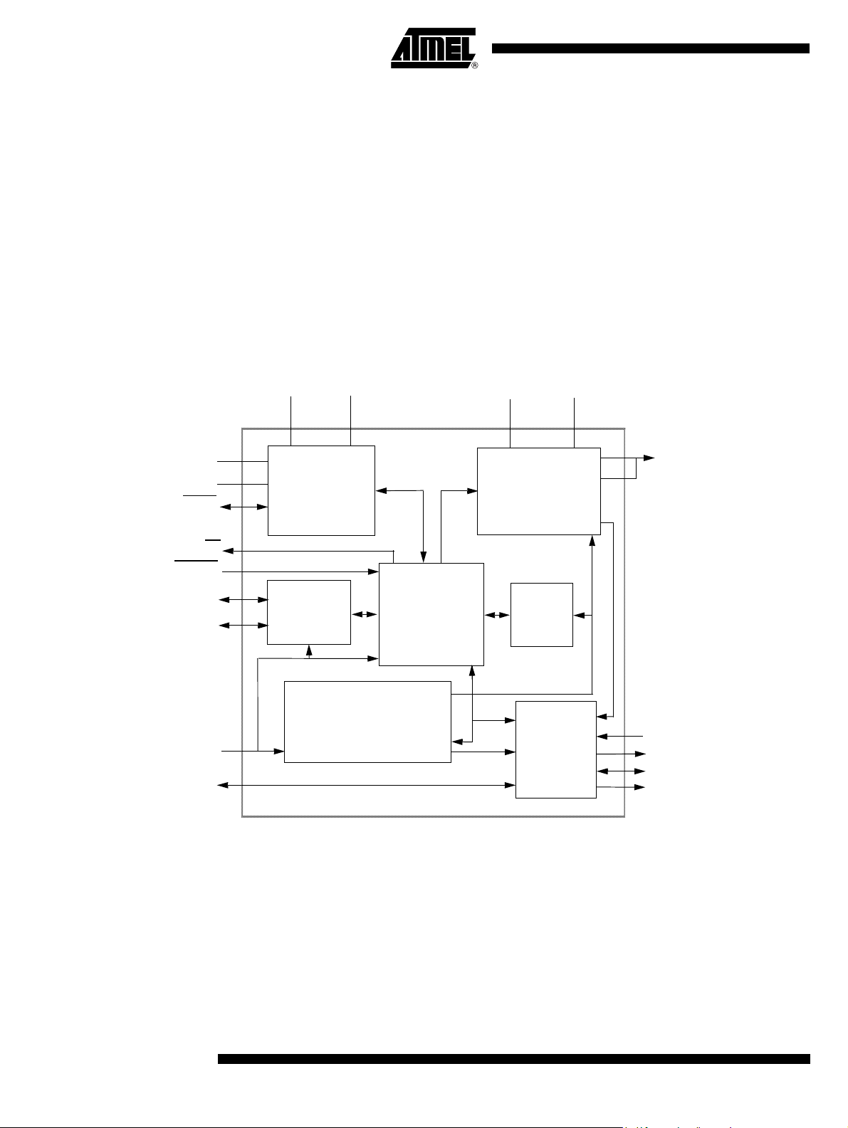
Block Diagram
DVCC
EVCC
RESET
PRES/ INT
A2/CK, A1/RST, A0/3V, CMDVCC
SCL
SDA
CLK
I/O, C4, C8
VCC
Voltage
supervisor
POR/PFD
TWI
Controller
Clocks Controller
VSS
Main
Control
& Logic Unit
LI
DC/DC
Converter
Timer
16 Bits
Analog
Drivers
CVSS
CVCC
CVCCIN
CPRES
CRST
CIO, CC4, CC8
CCLK
2
AT83C24
4234F–SCR–10/05
Page 3
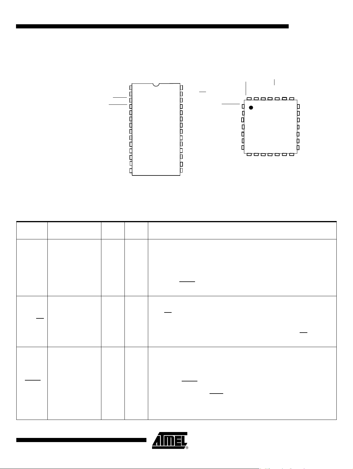
Pin Description
Pinouts (Top View) 28-pin SOIC Pinout QFN28 pinout
AT83C24
Signals
Table 1. Ports Description
Pad Name Pad Internal
Power Supply
A2/CK-
A1/RST-
A0/3V
EVCC 3 kV I
C8
1
DVCC
VSS
VCC
CVSS
CVCC
CRST
CCLK
NC
CC4
2
3
4
5
6
7
8
LI
9
10
11
12
13
14
RESET
CMDVCC
CVCCin
Note: 1. NC = Not Connected
2. SOIC and QFN packages are available for AT83C24 and for AT83C24NDS
ESD
Limits
Pad
Type
Description
Microcontroller Interface Function:
TWI bus slave address selection input.
A2/CK and A1/RST pins are respectively connected to CCLK and CRST signals in
“transparent mode” (see
A0/3V is used for hardware activation to select CVCC voltage (3V or 5V).
The slave address of the device is based on the value present on A2, A1, A0 on the
rising edge of
CLK rising edge.
CLK
28
RESET
DVCC
C8
27
26
28
1
2
V
CC
3
4
LI
5
6
7
8
9
CRST
QFN 28
TOP VIEW
101112
NC
CCLK
CLK
25
CC4
C4
PRES/INT
24
23
13
CC8
CPRES
I/O
22
EVCC
21
20
A2
/CK
19
A1
/RST
18
/3V
A0
17
SCL
16
SDA
15
NC
14
CIO
19
17
15
27
26
25
24
23
22
21
20
18
16
PRES/INT
C4
I/O
EVCC
/CK
A2
/RST
A1
/3V
A0
SCL
SDA
NC
CIO
CC8
CPRES
CMDVCC
VSS
CVSS
CVCC
CVCCin
page 17 ).
RESET pin (see Table 2). In fact, the address is taken internally at the 11th
PRES/INT EVCC
RESET VCC
4234F–SCR–10/05
3 kV
3 kV
O
open-
drain
I/O
open-
drain
Microcontroller Interface Function:
Depending on IT_SEL value (see CONFIG4 register),
PRES/INT outputs card presence status or interruptions (page 9)
An internal Pull-up (typ 330kΩ,see Table 18)to EVCC can be activated in the pad if
necessary using INT_PULLUP bit (CONFIG4 register).
Remark: during power up and before registers configuration, the PRES/INT signal must
be ignored.
Microcontroller Interface Function:
• Power-on reset
• A low level on this pin keeps the AT83C24 under reset even if applied on power-on.
It also resets the AT83C24 if applied when the AT83C24 is running (see Power
monitoring §).
• Asserting RESET when the chip is in Shut-down mode returns the chip to normal
operation.
• AT83C24 is driving the Reset pin Low on power-on-reset or if power fail on VCC or
DVCC (see POWERMON bit in CONFIG4 register), this can be used to reset or
interrupt other devices. After reset, AT83C24 needs to be reconfigured before
starting a new card session.
3
Page 4
Table 1. Ports Description (Continued)
Pad Name Pad Internal
Power Supply
ESD
Limits
Pad
Type Description
SDA VCC
SCL VCC
I/O EVCC
C4 EVCC
C8 EVCC
CLK EVCC
CIO CVCC 8 kV+
CC4 CVCC 8 kV+
3 kV
3 kV
3 kV
3 kV I/O
3 kV I/O
3 kV
I/O
open-
drain
I/O
open-
drain
I/O
(pull-up)
(pull-up)
I
I/O
(pull-up)
I/O
(pull-up)
Microcontroller Interface Function
TWI serial data
Microcontroller Interface Function
TWI serial clock
Microcontroller Interface Function
Copy of CIO pin and high level reference for EVCC.
An external pull up to EVCC is needed on IO pin.
I/O is the reference level for EVCC if EVCC is connected to a capacitor.
This feature is unused if EVCC is connected to VCC.
Microcontroller Interface Function
Copy of Card CC4.
Microcontroller Interface Function
Copy of Card CC8.
Microcontroller Interface Function
Master Clock
Smart card interface function
Card I/O
Smart card interface function
Card C4
CC8 CVCC 8 kV+
CPRES VCC 8 kV+
CCLK CVCC 8 kV+ O
CRST CVCC 8 kV+ O
CMDVCC EVCC
VCC 3 kV+ PWR
LI 3 kV+ PWR
3 kV+
I/O
(pull-up)
I
(pull-up)
I
(pull-up)
Smart card interface function
Card C8
Smart card interface function
Card presence
An internal Pull-up to VCC can be activated in the pad if necessary using PULLUP bit
(CONFIG1 register).
Smart card interface function
Card clock
Smart card interface function
Card reset
Microcontroller Interface Function:
Activation/Shutdown of the smart card Interface.
Supply Voltage
VCC is used to power the internal voltage regulators and I/O buffers.
DC/DC Input
LI must be tied to VCC pin through an external coil (typically 4.7 μH) and provides the
current for the charge pump of the DC/DC converter.
It may be directly connected to VCC if the step-up converter is not used (see STEPREG
bit in CONFIG4 register and see minimum VCC values in
Table 21 (class B)).
Table 20 (class A) and
4
AT83C24
4234F–SCR–10/05
Page 5
Table 1. Ports Description (Continued)
Pad Name Pad Internal
Power Supply
CVCC 8 kV+ PWR
ESD
Limits
AT83C24
Pad
Type Description
Card Supply Voltage
CVCC is the programmable voltage output for the Card interface.
It must be connected to external decoupling capacitors (see page 34 and page 36).
CVCCin 8 kV+ PWR
DVCC 3 kV+ PWR
EVCC 3 kV+ PWR
CVSS 8 kV+ GND
VSS GND Ground
Card Supply Voltage
This pin must be connected to CVCC.
Digital Supply Voltage
Is internally generated and used to supply the digital core.
This pin has to be connected to an external capacitor of 100 nF and should not be
connected to other devices.
Extra Supply Voltage (Microcontroller power supply)
EVCC is used to supply the internal level shifters of host interface pins.
EVCC voltage can be supplied from the external EVCC pin connected to the host power
supply.
If EVCC cannot be connected to the host power supply, it must be tied to an external
capacitor. EVCC voltage can be generated internally by an automatic follow up of the
logic high level on the I/O pin. In this configuration, connect a 100 nF + 100kOhms in
parallel between EVCC pin and VSS pin.
DC/DC Ground
CVSS is used to sink high shunt currents from the external coil.
Note: ESD Test conditions: 3 positive and 3 negative pulses on each pin versus GND. Pulses generated
according to Mil/STD 883 Class3. Recommended capacitors soldered on CVCC and VCC pins.
4234F–SCR–10/05
5
Page 6
Operational Modes
TWI Bus Control The Atmel Two-wire Interface (TWI) interconnects componen ts on a uniq ue two-wire bu s, made
up of one clock line and one data line with speeds of up to 400 Kbits per second, based on a
byte-oriented transfer format.
The TWI-bus interface can be used:
– To configure the AT83C24
– To select the operating mode of the card: 1.8V, 3V or 5V
– To configure the automatic activation sequence
– To start or stop sessions (activation and de-activation sequences)
– To initiate a warm reset
– To control the clock to the card in active mode
– To control the clock to the card in stand-by mode (stop LOW, stop HIGH or running)
– To enter or leave the card stand-by or power-down modes
– To select the interface ( connection to the host I/O / C4/ C8)
– To request the status (card present or not, over-current and out of range supply
voltage occurrence)
– To drive and monitor the card contacts by software
– To accurately measure the ATR delay when automatic activation is used
TWI Commands
Frame Structure The structure of the TWI bus data frames is made of one or a series of write and read com-
mands completed by STOP.
Write commands to the AT83C24 have the structure:
ADDRESS BYTE + COMMAND BYTE + DATA BYTE(S)
Read commands to the AT83C24 have the structure:
ADDRESS BYTE + DATA BYTE(S)
The ADDRESS BYTE is sampled on A2/CK, A1/RST, A0/3V after each reset (hard/soft/general
call) but A2/CK, A1/RST, A0/3V can be used for transparent mode after the reset.
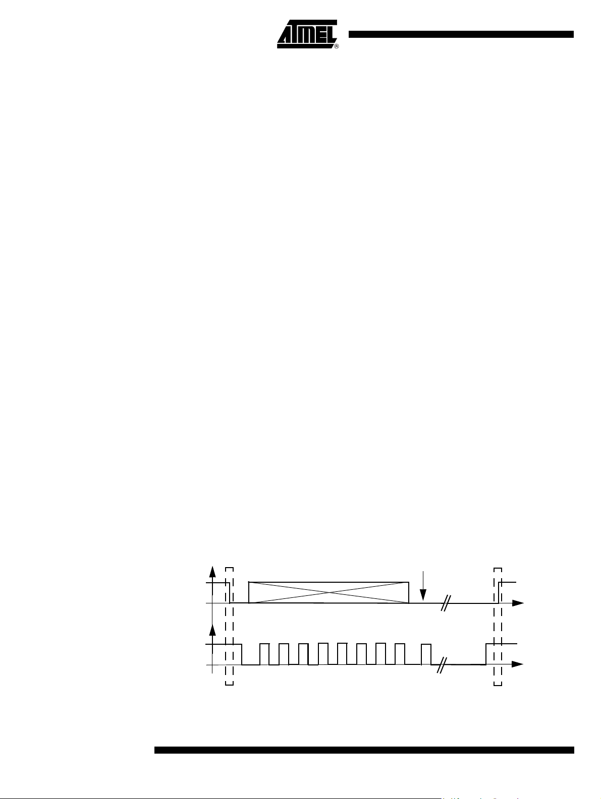
Figure 1. Data transfer on TWI bus
acknowledgement
SDA
SCL
Adresse byte
123456
from slave
78
command
and/or data
9
start condition
6
AT83C24
stop condition
4234F–SCR–10/05
Page 7
AT83C24
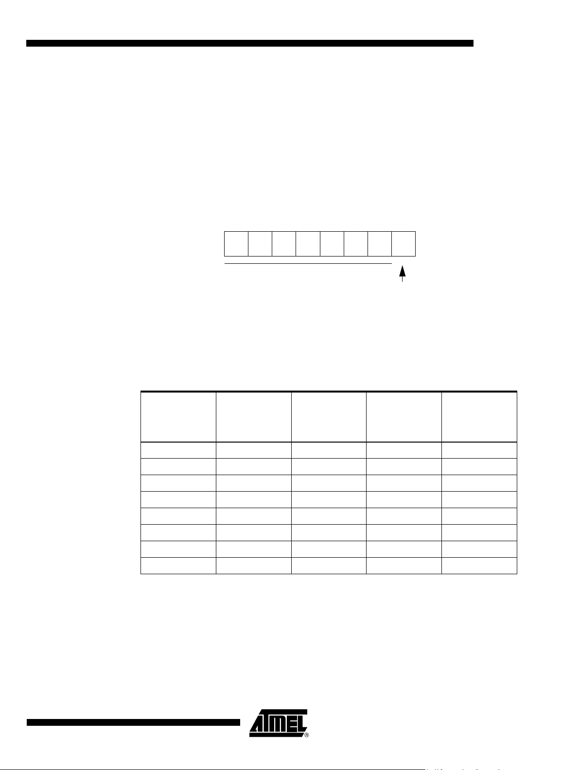
Address Byte The first byte to send to the device is the address byte. The device controls if the hardware
address (A2/CK, A1/RST, A0/3V pins on reset) corresponds to the address given in the
address byte (A2, A1, A0 bits).
If the level is not stable on A2/CK pin (or A1/RST pin, or A0/3V pin) at reset, the user has to send
the commands to the possible address taken by the device.
If A2/CK to A0/3V are tied to the host microcontroller and their reset values are unknown, a general call on the TWI bus allows to reset all the AT83C24 devices and set their address after
A2/CK to A0/3V are fixed.
Figure 2. Address Byte
b7 b6 b5
1
0
Slave Address on 7 Bits
0
b4
b3 b2 b1
0
A2
A1
1 for READ Command
0 for WRITE Command
A0
b0
R/W
Up to 8 devices can be connected on the sam e TWI bus. Each device is configured with a differ ent combination on A2/CK, A1/RST, A0/3V pins. The corresponding address byte values for
read/write operations are listed below.
Table 2. Address Byte Values
A2
(A2/CK pin)
0 0 0 0x41 0x40
0 0 1 0x43 0x42
0 1 0 0x45 0x44
0 1 1 0x47 0x46
1 0 0 0x49 0x48
A1
(A1/RST pin)
A0
(A0/3V pin)
Address Byte
for
Read
Command
Address Byte
for
Write
Command
4234F–SCR–10/05
1 0 1 0x4B 0x4A
1 1 0 0x4D 0x4C
1 1 1 0x4F 0x4E
7
Page 8
Write Commands The write commands are:
1. Reset:
Initializes all the logic and the TWI interface as after a power-up or power-fail reset. If a
smart card is active when RESET falls, a deactivation sequence is performed. This is a onebyte command.
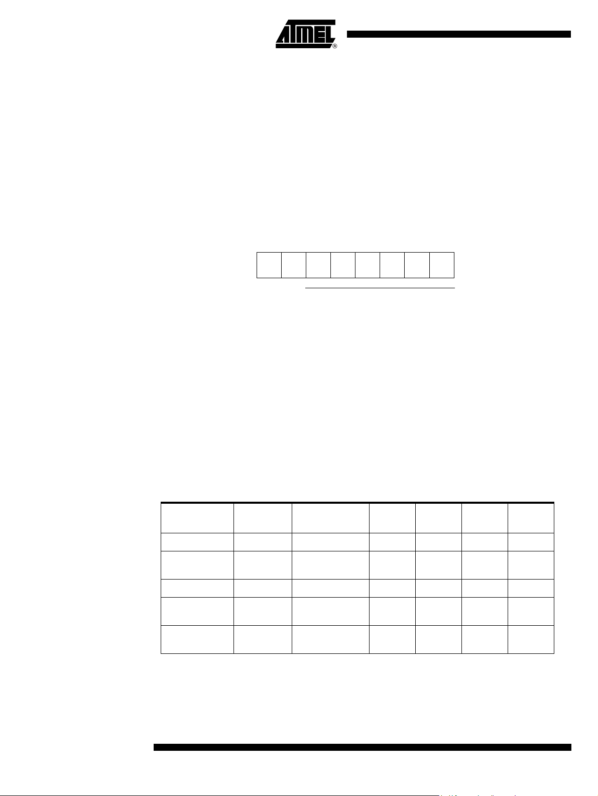
2. Write Config:
Configures the device according to the last six bits in the CONFIG0 register and to the fol-
lowing four bytes in CONFIG1, CONFIG2, CONFIG3 then CONFIG4 registers. This is a
five bytes command.
Figure 3. Command byte format for Write CONFIG0 command
b7 b6 b5 b4 b3 b2 b1
0
1
X
X
CONFIG0 on 6 Bits
X
X
b0
X
X
3. Write Timer:
Program the 16-bit automatic reset transition timer with the following two bytes. This is a
three bytes command.
4. Write Interface:
Program the interface. This is a one-byte command. The MSB of the command byte is fixed
at 0.
5. General Call Reset:
A general call followed by the value 06h has the same effect as a Reset command.
Table 3. Write Commands Description
Address Byte
(See Table 2) Command Byte
Data Byte 1Data Byte 2Data Byte 3Data Byte
4
1. Reset 0100 A2A1A00 1111 1111
2. Write config
3. Write Timer 0100 A2A1A00 1111 1100 TIMER1 TIMER0
4. Write Interface
5. General Call
Reset
8
AT83C24
0100 A2A1A00
0100 A2A1A00
0000 0000 0000 0110
(10 + CONFIG0 6
bits)
(0+INTERFACE 7
bits)
CONFIG1 CONFIG2 CONFIG3 CONFIG4
4234F–SCR–10/05
Page 9
AT83C24
Read Command After the slave address has been configured, the read command allows to read one or several
bytes in the following order:
• ST A TUS, CONFIG0, CONFIG1, CONFIG2, CONFIG3, INTERF ACE, TIMER1, TIMER0,
CAPTURE1, CAPTURE0
• FFh is completing the transfer if the microcontroller attempts to read beyond the last byte.
Note: Flags are only reset after the corresponding byte read has been acknowledged by the master.
Table 4. Read Command Description
Byte Description Byte Value
Address byte 0100 A2A1A01
Data byte 1 STATUS
Data byte 2 CONFIG0
Data byte 3 CONFIG1
Data byte 4 CONFIG2
Data byte 5 CONFIG3
Data byte 6 CONFIG4
Data byte 7 INTERFACE
Data byte 8 TIMER 1 (MSB)
Data byte 9 TIMER 0 (LSB)
Data byte 10 CAPTURE 1 (MSB)
Data byte 11 CAPTURE 0 (LSB)
Data byte 12 0xFF
Interrupts The PRES/INT behavior depends on IT_SEL bit value (see CONFIG4 register).
• If IT_SEL= 0, the PRES/INT output is High by default (on chip pull up or open drain).
PRES/
INT is driven Low by any of the following event:
– INSERT bit set in CONFIG0 register (card insertion/extraction or bit set by software )
– VCARD_INT bit set in STATUS register (the DC/DC output voltage has settled)
– over-current detection on CVCC
– VCARDERR bit set in CONFIG0 register (out of range vol t age on CVCC or bit set b y
software)
– ATRERR bit set in CONFIG0 register (no ATR before the card clock counter
overflows or bit set by software).This control of ATR timing is only available if ART bit
=1.
If IT_SEL=0, a read command of STATUS register and of CONFIG0 register will release
PRES/
INT pin to high level.
Several AT83C24 devices can share the same interrupt and the microcontroller can identify
the interrupt sources by polling the status of the AT83C24 devices using TWI commands.
4234F–SCR–10/05
• If IT_SEL= 1 (mandatory for NDS applications and for software compatibility with existing
devices) the PRES/
INT output is High to indicate a card is present and none of the following
event has occured:
9
Page 10
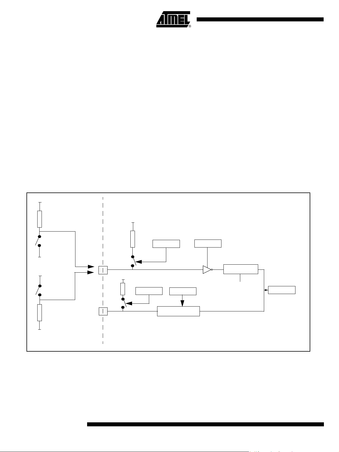
Card Presence Detection
The card presence is provided by the CPRES pin. The polarity of card presence contact is
selected with the CARDDET bit (see CONFIG1 register). A programmable filtering is controlled
with the CDS[2-0] bits (see CONFIG1 register).
An internal pull-up on the CPRES pin can be disconnected in order to reduce the consumption,
an external pull-up must then be connected to VCC. The PULLUP bit (see CONFIG1 register)
controls this feature.
The card presence switch is usually connected to Vss ( card present if CPRES=1). The CARDDET bit must be set. The internal pull up can be connected.
If the card presence contact is connected to Vcc (card present if CPRES=0), the internal pull-up
must be disconnected (see PULLUP bit) and an external pull-down must be connected to the
CPRES pin.
An interrupt can be generated if a card is inserted or extracted (see interrupts §).
Figure 4. Card Presence Input
VCC
– over-current detection on CVCC
– VCARDERR bit set in CONFIG0 register (out of range vol t age on CVCC or bit set b y
software)
VSS
VCC
VSS
External
Pull-up
Card
Contact
Presence
Card
Contact
Presence
External
Pull-down
CPRES
PRES/INT
VCC
(See Table 18)
Internal
Pull-up
EVCC
= 1 Closed
= 0 Open
INT_PULLUP Bit
PULLUP Bit CARDDET Bit
= 1 Closed
= 0 Open
IT_SEL Bit
IT Controller
= 1 No Card if CPRES = 0
= 0 No Card if CPRES = 1
FILTERING
CDS[2-0]
CARDIN bit
= 1 Card Inserted
= 0 No Card
10
AT83C24
4234F–SCR–10/05
Page 11
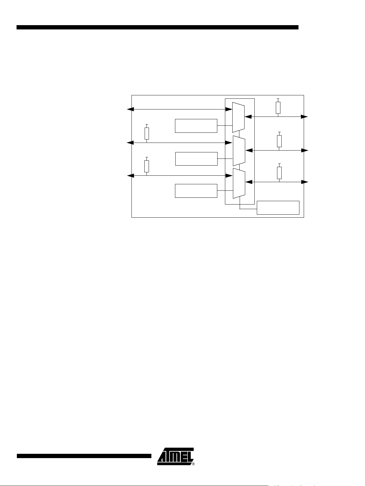
CIO, CC4, CC8 Controller
The CIO, CC4, CC8 output pins are driven re spectively by CARDIO, CARDC4, CARDC8 bits
values or by I/O, C4, C8 signal pins. This selection depends of the IODIS bit value. If IODIS is
reset, data are bidirectional between respectively I/O, C4, C8 pins and CIO, CC4, CC8 pins.
Figure 5. CIO, CC4, CC8 Block Diagram
I/O
AT83C24
CVCC
0
CIO
EVCC
C4
EVCC
C8
IO and CIO pins are linked together thro ugh the on chip level shifters if IODIS bit=0 in INTERFACE register. This is done automatically during an hardware activation.
Their iddle level are 1. With IO high, CIO is pulled up.
The same behavior is applicable on C4/ CC4 and C8/ CC8 pins.
The maximum frequency on those lines depends on CLK frequency (3 clock rising edges to
transfer). With CLK=27MHz, the maximum fre q uen cy on this lin e is 1.5MHz.
Due to the minimum transfer delay allowed for NDS applications, the CLK minimum frequ ency is
18MHz.
CARDIO bit
CARDC4 bit
CARDC8 bit
1
CVCC
0
1
CVCC
0
1
IODIS bit
CC4
CC8
Clock Controller The clock controller generates two clocks (as shown in Figure 6 and Figure 7):
1. a clock for the CCLK: Four different sources can be used: CLK pin, DCCLK signal,
CARDCK bit or A2/CK pin (in transparent mode).
2. a clock for DC/DC converter.
4234F–SCR–10/05
11
Page 12
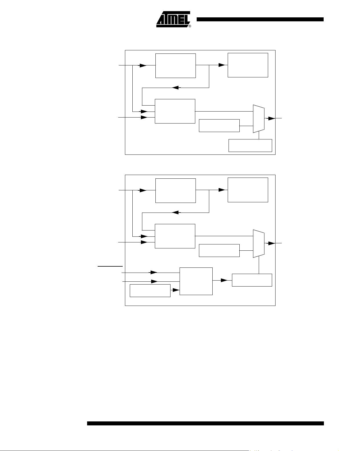
Figure 6. Clock Block Diagram with Software Activation (see page 14)
CLK
A2/CK
Figure 7. Clock Block Diagram with Hardware Activation (see page 14)
CLK
DCK[2:0]
CKS[2:0]
DCK[2:0]
DCCLK
CARDCK bit
DCCLK
DC/DC
0
1
CKSTOP bit
DC/DC
CCLK
A2/CK
CMDVCC
A1/RST
CRST_SEL bit
CKS[2:0]
CARDCK bit
Hardware
activation
CKSTOP bit
0
1
CCLK
CRST Controller The CRST output pin is driven by the A1 /RST pin signal pin or by the CARDRST bit value. This
selection depends of the CRST_SEL bit value (see CONFIG4 register).
If the CRST pin signal is driven by the CARDRST bit value, two modes are available:
• If the ART bit is reset, CRST pin is driven by CARDRST bit.
• If the ART bit is set, CRST pin is controlled and follows the “Automatic Reset Transition”
(
page 15).
12
AT83C24
4234F–SCR–10/05
Page 13
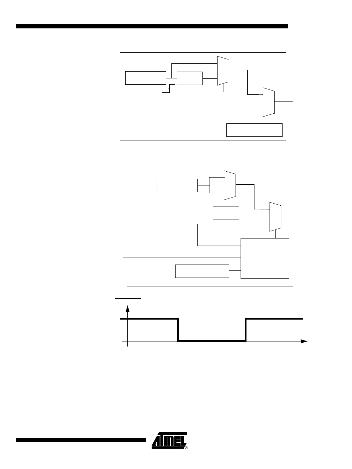
Figure 8. CRST Block Diagram with soft activation
AT83C24
0
CARDRST bit
Figure 9. CRST Block Diagram with Hardware Activation (CMDVCC pin used)
CARDRST bit
A1/RST
tb delay
see Fig 12
1
ART bit
ART bit
0
1
CRST_SEL bit = 0
0
1
CRST
0
1
CRST
CMDVCC
CMDVCC
Hardware
activation
CRST_SEL bit = 1
deactivation
activation
4234F–SCR–10/05
13
Page 14

Activation Sequence
Hardware Activation (DC/DC started with CMDVCC)
Initial conditions:
CARDDET bit must be configured in accordance to the smart card connector polarity.
IT_SEL bit, CRST_SEL bit (see CONFIG4 register) must be set and CARDRST bit (see INTER-
FACE register) must be cleared. A smart card must be detected to enable to start the DC/DC
(CVCC= 3V or 5V).
The hardware activation sequence is started by hard ware with CMDVCC pin going high to low. It
follows this automatic sequence:
• CIO / CC4 / CC8 and IO / C4 / C8 are respectively linked together (IODIS bit is cleared).
• The DC/DC is started and CVCC is set according to the A0/3V pin: 5V (Class A) if A0/3V is
High and 3V (Class B) is A0/3V is Low.
• CCLK signal is enabled (CKSTOP bit cleared) when CVCC has settled to the programmed
voltage (see Electrical Characteristics) and the level on A1/RST is 0. The CCLK so ur ce can
be DCCLK signal, CLK signal , A2/CK signals or CARDCK bit (see Figures 5).
• CRST signal is linked with A1/RST pin as soon as A1/RST pin level is 0. A rising edge on
A1/RST pin set the CRST pin.
Note: 1. The card must be deactivated to change the voltage.
Figure 10. Activation sequence with CMDVCC
CMDVCC
A1/RST
CCLK
CVCC
CRST
CIO
14
Note: For NDS applications, the host usually starts activation with A1/RST = 0.
AT83C24
4234F–SCR–10/05
Page 15

Software Activation (DC/DC Started With Writing in VCARD[1:0] bits) and ART bit = 1
Initial conditions: CARDRST bit = 0, CKSTOP bit =1, IODIS bit = 1.
The following sequence can be applied:
1. Card Voltage is set by software to the required value (VCARD[1:0] bits in CONFIG0
register). This writing starts the DC/DC.
2. Wait the end of the DC/DC init with a polling on VCARDOK bit (STATUS register) or
wait for PRES/
INT to go Low if enabled (if IT_SEL bit = 0 in CONFIG4 register).
When VCARDOK bit is set (by hardware), CARDIO bit should be set by software.
3. CKSTOP, IODIS are programmed by software. CKSTOP bit is reset to have the
clock running. IODIS is reset to drive the I/O, C4, C8 pins and the CIO,CC4, CC8
pins according to each other.
4. CARDRST bit (see INTERFACE register) is set by software.
Automatic Reset Transition description:
A 16-bit counter starts when CARDRST bit is set. It counts card clock cycles. The CRST signal
is set when the counter reaches the TIMER[1-0] value which corresponds to the “tb” time (
11).The counter is reseted when the CRST pin is released and it is stopped at the first start bit of
the Answer To Request (ATR) on CIO pin.
The CIO pin is not checked during the first 200 clock cycles (ta on Figure 11). If the ATR arrives
before the counter reaches Timer[1-0] value, the activation sequence fails, the CRST signal is
not set and the Capture[1-0] register contains the value of the counter at the arrival of the ATR.
AT83C24
Figure
If the ATR arrives after the rising edge on CRST pin and before the card clock counter overflows
(65535 clock cycles), the activation sequence completes. The Cap ture[1-0] register contain s the
value of the counter at the arrival of the ATR (tc time on
Figure 11).
Figure 11. Software activation with ART bit = 1
CARDRST bit set
CVCC
4
3
1
CRST
CCLK
CIO
ta
2
tb
tc
4234F–SCR–10/05
15
Page 16

ISO 7816 constraints: ta = 200 card clock cycles
400 card clock cycles< = tb
400 card clock cycles< = tc < = 40000 card clock cycles
Note: Timer[1-0] reset value is 400.
Software Activation (DC/DC Started by Writing in VCARD[1:0] bits) and ART bit = 0
The activation sequence is controlled by software using TWI commands, depending on the
cards to support. For ISO 7816 cards, the following sequence can be applied:
1. Card Voltage is set by software to the required value (VCARD[1:0] bits in CONFIG0
register). This writing starts the DC/DC.
2. Wait of the end of the DC/DC init with a polling on VCARDOK bit (STATUS register)
or wait for PRES/
INT to go Low if enabled (if IT_SEL bit = 0 in CONFIG4 register).
When VCARDOK bit is set (by hardware), CARDIO bit should be set by software.
3. CKSTOP, IODIS are programmed by software. CKSTOP bit is reset to have the
clock running. IODIS is reset to drive the I/O, C4, C8 pins and the CIO,CC4, CC8
pins according to each other.
4. CRST pin is controlled by software using CARDRST bit (see INTERFACE register).
Figure 12. Software activation without automatic control (ART bit = 0)
CVCC
CRST
CCLK
CIO
1
3
4
ATR
2
Note: It is assumed that initially VCARD[1:0], CARDCK, CARDIO and CARDRST bits are cleared,
CKSTOP and IODIS are set (those bits are further explained in the registers description)
Note: The user should check the AT83C24 status and possibly resume the activation sequence if one
TWI transfer is not acknowledged during the activation sequence.
Deactivation Sequence
The card automatic deactivation is triggered when one the following condition occurs:
• ICARDERR bit is set by hardware
16
AT83C24
4234F–SCR–10/05
Page 17

AT83C24
• VCARDERR bit is set by hardware (or by software)
• INSERT is set and CARDIN is cleared (card extraction)
• SHUTDOWN is set by software
• CMDVCC goes from Low to High
• Power fail on VCC (see POWERMON bit in CONFIG4 register)
• Reset pin going low
It is a self-timed sequence which cannot be interrupted when started (see Figure 13). Each step
is separated by a delay based on Td equal to 8 periods of the DC/DC clock, typically 2 µs:
1. T0: CARDRST is cleared, SHUTDOWN bit set.
2. T0 + 5 x Td:CARDCK is cleared, CKSTOP, CARDIO and IODIS are set.
3. T0 + 6 x Td: CARDIO is cleared.
4. T0 + 7 x Td: VCARD[1-0] = 00.
Figure 13. Deactivation Sequence
CVCC
CRST
CCLK
CIO,
CC4,
CC8
t1
Notes: 1. Setting ICARDERR by software does not trigger a deactivation. VCARDERR can be used to
deactivate the card by software.
2. t1=5 to 5.5*Td, and t2=0.5*Td to Td.
t2
Td
T ransparent Mode If the microcontroller outputs ISO 7816 signals, a transparent m ode a llows to con nect RST/CL K
and I/O/C4/C8 signals after an electrical level control. The AT83C24 level shifters adapt the ca rd
signals to the smart card voltage selection.
The CRST and CCLK microcontroller signals can be respectively connected to the A1/RST and
A2/CK pins.
4234F–SCR–10/05
The CRST_SEL bit (in CONFIG4 register) selects standard or transparent configuration for the
CRST pin. CKS in CONFIG2 allows to select standard or transparent configuration for the CCLK
pin. So CCLK and CRST are independent. A2/CK to A0/3V inputs always give the TWI address
at reset. The A0/3V pin can be used for TWI addressing and easily connect two AT83C24
devices on the same TWI bus.
17
Page 18

Figure 14. Transparent Mode Description
Microcontroller
AT83C24
CCLK
CRST
CIO
CC4
CC8
A2/CK
A1/RST
I/O
C4
C8
CCLK
CRST
CIO
CC4
CC8
SMART CARD
Power Modes Two power-down modes are available to reduce the AT83C24 power consumption (see STUT-
DOWN bit in CONFIG1 register and LP bits in CONFIG3 register).
To enter in the mode number 4 (see Table 5), the sequence is the following:
– First select the Low-power mode by setting the LP bit
– The activation of the SHUTDOWN bit can then be done.
The AT83C24 exits Power-down if a software/hardware reset is done or if SHUTDOWN bit is
cleared. The AT83C24 is then active immediately.
Either a hardware reset or a TWI command clearing the SHUTDOWN bit can cause an exit from
Power-down. The internal registers retain their value during the shutdown mode.
In Power-down mode, the device is sleeping and waiting for a wake up condition.
To reduce power consumption, the User should stop the clock on the CLK input after setting the
SHUTDOWN bit. The clock can be enabled again just before exiting SHUTDOWN (at least 10
µs before a START bit on SDA).
Table 5. Power Modes Description
Typical
Mode
Number
Shutdown
Bit
1 0 X 0 11
2 0 X 1 11 70 mA Regulator mode: VCC = 5.25V, CVCC = 5V,
3 0 X X 00 3 mA DC/DC off, CLK = 10MHz, VCC=3V to 5V
4 1 0 X 00 90 µA The TWI interface of the AT83C24 is active
5 1 1 X 00 30 µA Pulsed mode of the internal 3V logic regulator
LP
STEPREG VCARD[1:0]
Bit
Supply
Current
160 mA
30 mA
Description
Step up mod e : VC C = 3V, CVCC = 5V,
Icard = 65mA
Icard = 0
Icvcc = 65mA
but its analog blocs are switched off to reduce
the consumption
18
AT83C24
4234F–SCR–10/05
Page 19

Power Monitoring The AT83C24 needs only one power supply to run: VCC.
If the microcontroller outputs signals with a different electrical level, the host positive supply is
connected to EVCC.
EVCC and VCC pins can be connected together if they have the same voltage.
• If EVCC and VCC have different electrical levels:
The EVCC pin and RESET pin should be connected with a resistor bridge. RESET pin high
level must be higher than VIH (see Table 19). When EVCC drops, RESET pin level drops
too. A deactivation sequence starts if a card was active.
Then the AT83C24 resets if RESET pin stays low.
• If EVCC and VCC have the same value, then they should be connected:
The AT83C24 integrates an internal 3V r egulato r to feed its logic from th e VCC supp ly. The
bit powermon allows the user to select if the internal PFD monitors VCC or the internal regulated 3V. If the PFD monitors VCC (POWERMON bit=0), a deactivation is performed if VCC
falls below VPFDP (see VPFDP value in the datasheet). Same deactivation is performed if
the internal 3V falls below VPFDP and POWERMON bit = 1.
AT83C24
4234F–SCR–10/05
19
Page 20

Registers
Table 6. CONFIG0 (Config Byte 0)
7 6 5 4 3 2 1 0
1 0 ATRERR INSERT ICARDERR VCARDERR VCARD1 VCARD0
Bit
Number
7-6 1-0 These bits cannot be programmed and are read as 1-0.
Bit Mnemonic Description
5 ATRERR
4 INSERT
3 ICARDERR
Answer to Reset Interrupt
This bit is set when the card clock counter overflows (no falling edge on CIO
is received before the overflow of the card clock counter).
This bit is cleared by hardware when this register is read. It can be set by
software for test purpose. The reset value is 0.
Card Insertion Interrupt
This bit is set when a card is inserted or extracted: a change in CARDIN value
filtered according to CDS[2-0]. After power up, if the level on CPRES pin is 0,
then INSERT bit is set.
It can be set by software for test purpose.
This bit is cleared by hardware when this register is read. It cannot be cleared
by software.
The reset value is 0.
Card Over Current Interrupt
This bit is set when an over current is detected on CVCC. It can be set by
software for test purpose (no card deactivation is performed, no IT is
performed).
This bit is cleared by hardware when this register is read. It cannot be cleared
by software.
The reset value is 0.
2 VCARDERR
1-0 VCARD[1:0]
Card Out of Range Voltage Interrupt
This bit is set when the output voltage goes out of the voltage range specified
by VCARD field. It can be set by software for test purpose and deactivate the
card.
This bit is cleared by hardware when this register is read. It cannot be cleared
by software.
The reset value is 0.
Card Voltage Selection
VCARD[1:0] = 00: 0V
VCARD[1:0] = 01: 1.8V (see STEPREG bit)
VCARD[1:0] = 10: 3V
VCARD[1:0] = 11: 5V
VCARD[1:0] writing to 1.8V, 3V, 5V starts the DC/DC if a card is detected.
VCARD[1:0] writing to 0 stops the DC/DC.
No card deactivation is performed when the voltage is changed between
1.8V, 3V or 5V. The microcontroller should deactivate the card before
changing the voltage.
The reset value is 00.
20
AT83C24
4234F–SCR–10/05
Page 21

Table 7. CONFIG 1 (Config Byte 1)
7 6 5 4 3 2 1 0
X ART SHUTDOWN CARDDET PULLUP CDS2 CDS1 CDS0
AT83C24
Bit
Number
7 X This bit should not be set.
6 ART
5
4 CARDDET
3 PULLUP
Bit
Mnemonic
SHUTDOWN
Description
Automatic Reset Transition
Set this bit to have the CRST pin changed according to activation sequence.
Clear this bit to have the CRST pin immediately following the value programmed
in CARDRST.
The reset value is 0.
Shutdown
Set this bit to reduce the power consumption. An automatic de-activation
sequence will be done.
Clear this bit to enable VCARD[1:0] selection.
The reset value is 0.
Card Presence Detection Polarity
Set this bit to indicate the card presence detector is closed when no card is
inserted (CPRES is low).
Clear this bit to indicate the card presence detector is open when no card is
inserted (CPRES is high).Changing CARDDET will set INSERT bit (see
CONFIG0) even if no card is inserted or extracted.
The reset value is 0.
Pull-up Enable
Set this bit to enable the internal pull-up on the CPRES pin. This allows to
minimize the number of external components.
Clear this bit to disable the internal pull-up and minimize the power consumption
when the card detection contact is on. Then an external pull-up must be
connected to V
The reset value is 1.
CC
(typically a 1 MΩ resistor).
4234F–SCR–10/05
2-0 CDS[2:0]
Card Detection filtering
CPRES is sampled by the master clock provided on CLK input. A change on
CPRES is detected after:
CDS[2-0] = 0: 0 sample
CDS[2-0] = 1: 4 identical samples
CDS [2-0] = 2: 8 identical samples (reset value)
CDS[2-0] = 3: 16 identical samples
CDS[2-0] = 4: 32 identical samples
CDS[2-0] = 5: 64 identical samples
CDS[2-0] = 6: 128 identical samples
CDS[2-0] = 7: 256 identical samples
The reset value is 2.
(1)
Note: W hen CDS[2-0] = 0 and IT_ SEL = 0, PRES/ INT = 1 when no
card is present and PRES/INT = 0 when a card is inserted
even if CLK is STOPPED. This can be used to wake up the
external microcontroller and restart CLK when a card is
inserted in the AT83C24.
If CDS[2-0] = 0, IT_SEL = 1 and CLK is stop ped, a card insertion or
extraction has no effect on PRES/
INT pin.
21
Page 22

Table 8. CONFIG2 (Config Byte 2)
7 6 5 4 3 2 1 0
X DCK2 DCK1 DCK0 X CKS2 CKS1 CKS0
Bit
Number
7 X This bit should not be set.
6-4 DCK[2:0]
3 X This bit should not be set.
2-0 CKS[2:0]
Bit
Mnemonic
Description
DC/DC Clock prescaler factor
DCCLK is the DC/DC clock. It is the division of CLK input by DCK prescaler.
DCK = 0: prescaler factor equals 1 (CLK = 4 to 4.61MHz)
DCK [2:0] = 1: prescaler factor equals 2 (CLK = 7 to 9.25MHz)
DCK [2:0] = 2: prescaler factor equals 4 (CLK = 14 to 18.5 MHz)
DCK [2:0] = 3: prescaler factor equals 6 (CLK = 21 to 27.6 MHz)
DCK [2:0] = 4: prescaler factor equals 8 (CLK = 28 to 34.8 MHz)
DCK [2:0] = 5: prescaler factor equals 10 (CLK = 35 to 43 MHz)
DCK [2:0] = 6: prescaler factor equals 12 (CLK = 43.1 to 48 MHz)
DCK [2:0] = 7: reserved
The reset value is 1.
DCCLK must be as close as possible to 4 MHz with a duty cycle of 50%.
DCK must be programmed before starting the DC/DC.
The other values of CLK are not allowed.
DCK has to be properly configured before resetting the STEPREG bit.
Card Clock prescaler factor
CKS [2:0] = 0: CCLK = CLK (then the maximum frequency on CLK is 24 MHz)
CKS [2:0] = 1: CCLK = DCCLK (DC/DC clock)
CKS [2:0] = 2: CCLK = DCCLK / 2
CKS [2:0] = 3: CCLK = DCCLK / 4
CKS [2:0] = 4: CCLK = A2
CKS [2:0] = 5: CCLK = A2 / 2
CKS [2:0] = 6: CCLK = CLK / 2
CKS [2:0] = 7: CCLK = CLK / 4
The reset value is 0.
22
Notes: 1. When this register is changed, a special logic insures no glitch occurs on the CCLK pi n and
actual configuration changes can be delayed by half a period to two periods of CCLK.
2. CCLK must be stopped with CKSTOP bit before switching from CKS = (0, 1, 2, 3, 6, 7) to CKS
= (4, 5) or vice versa.
3. When DCK = 0, only CKS=4 and CKS=5 are allowed.
4. The user can’t directly select A2 or A2/2 after a reset or when switching from CKS = (0, 1, 2, 3,
6, 7) to CKS = (4, 5). To select A2, the user should select A2/2 first and after A2. To select
A2/2, the user should select A2 first and after A2/2.
AT83C24
4234F–SCR–10/05
Page 23

Table 9. CONFIG3 (Config Byte 3)
7 6 5 4 3 2 1 0
EAUTO VEXT1 VEXT0 ICCADJ LP X X X
AT83C24
Bit
Number
7-5
4 ICCADJ
3 LP
Bit
Mnemonic
EAUTO
VEXT1
VEXT0
Description
EVCC voltage configuration:
EAUTO VEXT1 VEXT0
0 0 0 EVCC = 0 the regulator is switched off.
0 0 1EVCC = 2.3V
0 1 0 EVCC = 1.8V
0 1 1 EVCC = 2.7V
1 X X EVCC voltage is the level detected on I/O input pin.
if EVCC is supplied from the external EVCC pin, the user can switch off the
internal EVCC regulator to decrease the consumption.
If EVCC is switched off, and no external EVCC is supplied, the AT83C24 is
inactive until a hardware reset is done.
The reset value is 100.
CICC overflow adjust
This bit controls the DC/DC sensitivity to any overflow current .
Set this bit to decrease the DC/DC sensitivity (CI
20%, see Electrical Characteristics). The start of the DC/DC with a high current
load is easier.
Clear this bit to have a normal configuration.
The reset value is 0.
Low-power Mode
Set this bit to enable low-power mode during shutdown mode (pulsed mode
activated).
Clear this bit to disable low-power mode during shutdown mode.
The activation reference is the following:
• First select the Low-power mode by setting LP bit.
• The activation of SHUTDOWN bit can then be done.
This bit as no effect when SHUTDOWN bit is cleared.
The reset value is 0.
is increased by about
CC_ovf
4234F–SCR–10/05
2 X This bit should not be set.
1
0 X This bit should not be set.
X
This bit should not be set.
23
Page 24

Table 10. CONFIG4 (Config Byte 4)
7 6 5 4 3 2 1 0
X X X STEPREG INT_PULLUP POWERMON IT_SEL CRST_SEL
Bit Number Bit Mnemonic Description
7-5 X-X-X These bits should not be set.
Step Regulator mode
Clear this bit to enable the automatic step-up converter (CVCC is stable even if VCC is not higher than CVCC).
Set this bit to permanently disable the step-up converter (CVCC is stable only if VCC is sufficiently higher than
4 STEPREG
3 INT_PULLUP
2 POWERMON
CVCC).
This bit must be set before activating the DC/DC converter if no external coil is present.
The reset value is 0.
This bit must always be set if no external coil is used
Internal pull-up
Set this bit to activate the internal pull-up (connected internally to EVCC) on PRES/INT pin.
Clear this bit to deactivate the internal pull-up.
PRES/INT is an open drain output with a programmable internal pull up.
The reset value is 0.
Power monitor
Set this bit to monitor any glitch on the Digital Supply Voltage (DVCC) of the AT83C24.
Clear this bit to monitor any glitch on VCC.
The reset value is 0.
1 IT_SEL
0 CRST_SEL
Interrupt Select
Set this bit to disable INSERT and VCARD_INT interrupts. Then PRES/INT is pulled up when a card is present
and no error is detected.
Clear this bit to have all the interrupt sources enabled and active Low.
IT_SEL must be set to enable a hardware activation with CMDVCC.
The reset value is 0.
Card Reset Selection
Set this bit to have the CRST pin driven by hardware through the A1 pin (only with hardware activation).
Clear this bit to have the CRST pin driven by software through the CARDRST bit.
CRST_SEL must be set when CMDVCC is used (hardware activation).
The reset value is 0.
24
AT83C24
4234F–SCR–10/05
Page 25

Table 11. INTERFACE (Interface Byte)
7 6 5 4 3 2 1 0
0 IODIS CKSTOP CARDRST CARDC8 CARDC4 CARDCK CARDIO
Bit Number Bit Mnemonic Description
7 0 This bit should not be set.
Card I/O isolation
Set this bit to drive the CIO, CC4, CC8 pins according to CARDIO, CARDC4, CARDC8 respectively and to put
I/O, C4, C8 in Hi-Z. This can be used to have the I/O, and C4 and C8 pins of the host communicating with
6 IODIS
5 CKSTOP
another AT83C24 interface, while CIO, CC4 and CC8 are driven by software (or if the card is in standby or
power-down modes).
Clear this bit to drive the I/O/CIO, C4/CC4 and C8/CC8 pins according to each other. This can be used to activate
asynchronous cards.
The reset value is 1.
CARD Clock Stop
Set this bit to stop CCLK according to CARDCK. This can be used to set asynchronous cards in power-down
mode (GSM) or to drive CCLK by software.
Clear this bit to have CCLK running according to CKS. This can be used to activate asynchronous cards.
Note: 1. When this bit is changed a special logi c ensures that no glitch oc curs on the CCLK pin
AT83C24
and actual configuration changes can be delayed by half a period to two periods of
CCLK.
2. CKSTOP must be set before switching on the DC/DC with VCARD[1:0].
4 CARDRST
3 CARDC8
2 CARDC4
1 CARDCK
0 CARDIO
The reset value is 1.
Card Reset
Set this bit to enter a reset sequence according to ART bit value.
Clear this bit to drive a low level on the CRST pin.
The reset value is 0.
Card C8
Set this bit to drive the CC8 pin High with the on-chip pull-up (according to IODIS bit value). The pin can then be
an input (read in STATUS register).
Clear this bit to drive a low level on the CC8 pin (according to IODIS bit value).
The reset value is 0.
Card C4
Set this bit to drive the CC4 pin High with the on-chip pull-up (according to IODIS bit value). The pin can then be
an input (read in STATUS register).
Clear this bit to drive a low level on the CC4 pin (according to IODIS bit value).
The reset value is 0.
Card Clock
Set this bit to set a high level on the CCLK pin (according to CKSTOP bit value).
Clear this bit to drive a low level on the CCLK pin.
The reset value is 0.
Card I/O
Set this bit to drive the CIO pin High with the on-chip pull-up (according to IODIS bit value). The pin can then be
an input (read in STATUS register).
Clear this bit to drive a low level on the CIO pin (according to IODIS bit value).
The reset value is 0.
4234F–SCR–10/05
25
Page 26

Table 12. STATUS (Status Byte)
7 6 5 4 3 2 1 0
CC8 CC4 CARDIN VCARDOK X VCARD_INT CRST CIO
Bit Number Bit Mnemonic Description
7 CC8
6 CC4
5 CARDIN
4 VCARD_OK
3 X This bit should not be set.
2 VCARD_INT
Card CC8
This bit provides the actual level on the CC8 pin when read.
The reset value is 0.
Card CC4
This bit provides the actual level on the CC4 pin when read.
The reset value is 0.
Card Presence Status
This bit is set when a card is detected.
It is cleared otherwise.
Card Voltage Status
This bit is set by the DCDC when the output voltage remains within the
voltage range specified by VCARD[1:0] bits.
It is cleared otherwise.
The reset value is 0.
Card voltage interrupt
This bit is set when VCARD_OK bit is set.
This bit is cleared when read by the microcontroller.
The reset value is 0.
1 CRST
0 CIO
Table 13. TIMER 1 (Timer MSB)
7 6 5 4 3 2 1 0
Bit 15 Bit 14 Bit 13 Bit 12 Bit 11 Bit 10 Bit 9 Bit 8
Bit
Number
7 - 0 Bits 15 - 8 Timer MSB (bits 15 to 8)
Bit
Mnemonic
Description
Reset value = 0x00000001
Card RST
This bit provides the actual level on the CRST pin when read.
The reset value is 0.
Card I/O
This bit provides the actual level on the CIO pin when read.
The reset value is 0.
26
AT83C24
4234F–SCR–10/05
Page 27

Table 14. TIMER 0 (Timer LSB)
7 6 5 4 3 2 1 0
Bit 7 Bit 6 Bit 5 Bit 4 Bit 3 Bit 2 Bit 1 Bit 0
AT83C24
Bit
Number
7 - 0 bits 7 - 0 Timer LSB (bits 7to 0)
Bit
Mnemonic
Description
Reset value = 0x10010000
Table 15. CAPTURE 1 (Capture MSB)
7 6 5 4 3 2 1 0
bit 15 bit 14 bit 13 bit 12 bit 11 bit 10 bit 9 bit 8
Bit
Number
7 - 0 bits 15 - 8 See “software activation with ART = 1”, page 15.
Bit
Mnemonic
Description
Reset value = 0x00000000
Table 16. CAPTURE 0 (Capture LSB)
7 6 5 4 3 2 1 0
bit 7 bit 6 bit 5 bit 4 bit 3 bit 2 bit 1 bit 0
Bit
Number
Bit
Mnemonic
Description
4234F–SCR–10/05
7 - 0 bits 7 - 0 See “software activation with ART = 1”, page 15.
Reset value = 0x00000000
27
Page 28

Electrical Characteristics
Absolute Maximum Ratings
Ambient Temperatu r e Under Bias: .....................-40°C to 85°C
Storage Temperature:................................... -65°C to +150°C
Voltage on VCC: ........................................V
Voltage on SCIB pins (***):.........CVSS -0.5V to CVCC + 0.5V
*
*NOTICE: S tresses at or above those listed under “Absolute
Maximum Ratings” may cause permanent damage to the device. This is a stress rating only and
functional operation of the device at these or any
-0.5V to +6.0V
SS
other conditions above those indicated in the
operational sections of this specification is not
implied. Exposure to absolute maximum rating
conditions may affect device reliability.
Voltage on host interface pins:.......VSS -0.5V to EVCC + 0.5V
Voltage on other pins:......................VSS -0.5V to VCC + 0.5V
Power Dissipation value is based on the maximum allowable die temperature and the thermal
resistance of the package.
Power Dissipation: .......................................................... 1.5W
Thermal resistor of QFN pack-
age..(**)............................35°C/W
Thermal resistor of SO package.................................48°C/W
(**) Exposed die attached pad must be soldered to ground
Thermal resistor are measured on multilayer PCB with 0 m/s air flow.
(***) including shortages between any groups of smart card pins.
AC/DC Parameters EVCC connected to host power supply: from 1.6V to 5.5V.
TA = -40°C to +85°C; VSS = 0V; VCC = 3V to 5.5V.
CLASS A card supplied with CVCC = 4.75 to 5.25V for AT83C24NDS
CLASS A card supplied with CVCC = 4.6 to 5.25V for AT83C24
CLASS B card supplied with CVCC = 2.8V to 3.2V
CLASS C card supplied with CVCC = 1.68V to 1.92V
Table 17. Core (VCC)
Symbol Parameter Min Typ Max Unit Test Conditions
V
PFDP
V
PFDM
t
rise, tfallVDD
Power fail high level threshold 2.4 2.5 2.6 V
Power fail low level threshold 2.25 2.35 2.45 V
rise and fall time 1 μs 600s Not tested.
Table 18. Host Interface (I/O, C4, C8, CLK, A2, A1, A0, CMDVCC, PRES/INT)
Symbol Parameter Min Typ Max Unit Test Conditions
V
V
Input Low-voltage -0.5
IL
Input High Voltage 0.7 x EVCC EVCC + 0.5 V
IH
0.3 x EVCC
0.25 x EVCC
EVCC from 2.7V to VCC
V
EVCC from 1.6 to 2.7V
EAUTO=0
EAUTO=1
EVCC from 1.6V to VCC
28
AT83C24
4234F–SCR–10/05
Page 29

AT83C24
Table 18. Host Interface (I/O, C4, C8, CLK, A2, A1, A0, CMDVCC, PRES/INT) (Continued)
Symbol Parameter Min Typ Max Unit Test Conditions
V
V
EI
R
PRES/INT
Output Low-voltage (I/O, C4, C8, PRES/INT)
OL
Output High Voltage (C4, C8, PRES/INT)
OH
V
on I/O depends on external pull up value
OH
Extra Supply Current +3 mA CL = 100 nF
CC
0.8 x EVCC EVCC V
PRES/INT weak pull-up output current 300 330 360 κΩ
0.05
0.4
EVCC EVCC pin not connected to a power supply Vpeak - 10 mV Vpeak Vpeak + 25 mV V
EVCC EVCC pin connected to a power supply
Vpeak -
200mV
CLK Clock signal for AT83C24 4 48 MHz
VVIOL = -100 μA
I
-1.2 mA
OL =
EVCC from 1.6V to VCC
IOH = 100 μA
Short to VSS
INT_PULLUP = 0: Internal
pull-up active.
CL = 100 nF, EIcc = +3
mA
Vpeak on I/O from 1.6V to
VCC
EAUTO = 1:
min duration 1µs,
min frequency 0.1Hz,
spikes <50ns are filtered.
EAUTO = 1
If DCK[2:0] =0
(CLK=4MHz to 4.61MHz),
a duty cycle of 50% is
needed.
CLK Clock signal for AT83C24NDS 18 48 MHz
no constrainst on duty
cycle
Table 19. Host Interface (SCL, SDA, RESET)
Symbol Parameter Min Typ Max Unit Test Conditions
V
V
V
V
Input Low-voltage -0.5
IL
Input High Voltage
IH
Output Low-voltage 0.4 V IOL = -3 mA
OL
Input trigger hysteresis 0.1 x VCC
HIST
3
0.7 x VCC
1.9
0.3 x VCC
VCC + 0.5 V
VCC > 4.5V
V
VCC <= 4.5V
VCC > 4.5V
VCC <= 4.5V
Table 20. Smart Card Class A
Symbol Parameter Min Typ Max Unit Test Conditions
VCC=3V to 5.5V,
STEPREG=0
VCC > 5.35V, STEPREG = 1
CI
CC
CICC_ovf
Card Supply Current Capability 65
65
Card Supply Current Overflow:
ICCADJ = 0 (reset value)
ICCADJ = 1
66
66
120
130
130
150
mA
mA VCC from 3 to 5.5V
4234F–SCR–10/05
29
Page 30

Table 20. Smart Card Class A
Symbol Parameter Min Typ Max Unit Test Conditions
0 < Icard < 60mA CL =10µF
Ripple on CVCC
Spikes on CVCC 4.6 5.3 V
Vcardok up Vcardok high level threshold 4.8 4.9 V
60
150
200
350
for AT83C24
mV
0 < Icard < 65mA CL = 3.3µF
for AT83C24NDS
Max. charge 40 nA.s
Max. duration 400 ns
Max. Icard variation 200 mA
Vcardok down Vcardok low level threshold
T
VHL
T
VLH
CVCC valid to 0
CVCC 0 to Valid
4.6
4.75
4.8
4.8
180
500
180
110
240
170
250
750
250
250
300
250
AT83C24
V
AT83C24NDS
Icard = 0, VCC > V
CL = 3.3 μF Icard = 0
μs
CL = 10 μF Icard = 0
(see note 1)
VCC = 3V, CL = 3.3µF
Icard = 65mA
Icard = 0mA
μs
VCC = 3V, CL = 10µF
Icard = 65mA
Icard = 0mA
Notes: 1. Capacitor: X7R type or X5R type, max ESR value is 30mΩ (100kHz-100MHz),
Replacing 3.3µF by 2.2µF in parrallel with 1µF is better for ESR and noise reduction.
Table 21. Smart Card Class B
Symbol Parameter Min Typ Max Unit Test Conditions
CI
CC
CICC_ovf
Card Supply Current Capability
Card Supply Current Overflow:
ICCADJ = 0 (reset value)
ICCADJ = 1
65
65
66
66
130
140
140
150
VCC=3V to 5.5V, STEPREG=0
mA
VCC > 5.35V, STEPREG = 1
mA VCC from 3.0 to 5.5V
PFDP
Ripple on CVCC 60
Spikes on CVCC 2.76 3.24 V
Vcardok up Vcardok high level threshold 2.8 3 V
Vcardok
down
T
30
Vcardok low level threshold 2.76 2.9 V
VHL
CVCC valid to 0
130
400
AT83C24
200
350
250
500
0 < Icard < 65mA CL =10µF
mV
0 < Icard < 65mA CL = 3.3µF
Maxi. charge 40 nA.s
Max. duration 400 ns
Max. variation Icard 200mA
Icard = 0, VCC > V
CL = 3.3 μF Icard = 0
μs
(see note 1)
CL = 10 μF Icard = 0
PFDP
4234F–SCR–10/05
Page 31

AT83C24
Table 21. Smart Card Class B
Symbol Parameter Min Typ Max Unit Test Conditions
VCC = 3V, CL = 3.3µF
140
110
T
VLH
CVCC 0 to Valid
130
100
Notes: 1. Capacitor: X7R type or X5R type, max ESR value is 30mΩ (100kHz-100MHz),
Replacing 3.3µF by 2.2µF in parrallel with 1µF is better for ESR and noise reduction.
Table 22. Smart Card Class C
Symbol Parameter Min Typ Max Unit Test Conditions
250
250
250
250
Icard = 65mA
Icard = 0mA
μs
VCC = 3V, CL = 10µF
Icard = 60mA
Icard = 0mA
CI
Card Supply Current Capability 40 mA VCC = 3V
CC
Card Supply Current Overflow:
CICC_ovf
ICCADJ = 0 (reset value)
45 mA
ICCADJ = 1
Spikes on CVCC 1.68 1.92 V
Vcardok up Vcardok high level threshold 1.75 1.8 V
Vcardok
down
T
T
Vcardok low level threshold 1.7 1.75 V
CVCC valid to 0 180 300 μs
VHL
200
100
VLH
CVCC 0 to valid
50
60
300
150
80
100
Icard = 0, CL = 10 μF
CVCC = 1.8V to 0.4V
Icard = 40mA, CL = 10 μF
Icard = 0, CL = 10 μF
μs
Icard = 40mA, CL = 3.3 μF
Icard = 0, CL = 3.3 μF
CVCC = 0.4 to VCARDOK
Notes: 1. Capacitor: X7R type or X5R type, max ESR value is 30mΩ (100kHz-100MHz),
Replacing 3.3µF by 2.2µF in parrallel with 1µF is better for ESR and noise reduction.
Table 23. Smart Card Clock (CCLK pin)
Symbol Parameter Min Typ Max Unit Test Conditions
(1)
(1)
(1)
(1)
(1)
V
V
tR t
4234F–SCR–10/05
Output Low-voltage 0 0.4 V
OL
Output High Voltage
OH
I
Short Circuit Current -30 30 mA Short to GND or CVCC
OS
Rise and Fall time
F
CVCC - 0.45
0.7CVCC
CVCC
CVCC
16
22.5
50
IOL = -200 μA CLASS
A&B&C
IOH = +200 μA CLASS
A&B
V
CLASS C
C
30 pF CLASS A
L =
C
30 pF CLASS B
ns
L =
C
30 pF CLASS C
L =
measurement between
10% and 90% of CVCC
31
Page 32

Table 23. Smart Card Clock (CCLK pin) (Continued)
Symbol Parameter Min Typ M ax Unit Test Conditions
0.2
CLASS A
CCLK from 0.5 to 4.2V
Rise and Fall Slew rate
0.12 V/ns
CLASS B
CCLK from 0.5 to 0.85 x
CVCC
Low level voltage stability
(taking into account PCB design)
High level voltage stability
(taking into account PCB design)
-0.25 0.5 V CLASS A&B&C
4.2
2.35
CVCC-0.4
CVCC+0.25
CVCC+0.25
CVCC+0.25
CVCC = CLASS A
V
CVCC = CLASS B
CLASS C
CCLK Smart card clock frequency 24 MHz CL = 30pF, CLK=48MHz
Table 24. Smart Card I/O (CIO, CC4, CC8 pins)
Symbol Parameter Min Typ Max Unit Test Conditions
V
V
V
Input Low-voltage -0.3V 0.8 V IIL = 500 µA
IL
I
Input Low Current 700 µA CVCC = CLASS A&B&C
IL
Input High Voltage
IH
I
Input High Current -20 +20 μA
IH
Output Low-voltage 0
OL
0.6 x CVCC
0.7 x CVCC
CVCC
CVCC
0.45
0.3
0.3
CVCC = CLASS A
V
CVCC = CLASS B & C
IOL = -1 mA CLASS A
V
IOL = -1 mA CLASS B
IOL = -1 mA CLASS C
V
I
tR t
tR t
Output High Voltage
OH
Output Short Circuit Current -15 +15 mA Short to GND or CVCC
OS
Low level voltage stability
(taking into account PCB design)
High level voltage stability
(taking into account PCB design)
0.75 x CVCC
0.9 x CVCC
-0.25
-0.25
-0.25
CVCC-0.5 CVCC+0.25 V CVCC = CLASS A&B&C
CVCC
CVCC
0.6
0.4
0.4
IOH = 40 μA CLASS
A&B&C
V
IOH = 0μA, CLASS A&B
CLASS A
V
CLASS B
CLASS C
CL = 65 pF
CLASS A:
Output rise and fall time
F
0.1 μs
measurement between
0.6V and 70% of CVCC
CLASS B & C:
measurement between
0.4V and 70% of CVCC
Input rise and fall time 1 μs CL = 65 pF
F
32
AT83C24
4234F–SCR–10/05
Page 33

AT83C24
Table 25. Smart Card RST (CRST pin)
Symbol Parameter Min Typ Max Unit Test Conditions
0.12 x CVCC
V
Output Low-voltage
OL
0
0
0.4
0.2
IOL = -20 µA CLASS
A&B&C
V
IOL = -200 µA CLASS A
IOL = -200 µA CLASS
B&C
V
I
Output High Voltage 0.9*CVCC CVCC V
OH
Output High Current -15 +15 mA Short to GND or CVCC
OS
IOH = 200 µA
CLASS A&B&C
CL = 30pF
tR t
Rise and Fall time 0.1 µs
F
measurement between
10% and 90% of CVCC
Low level voltage stability
(taking into account PCB design)
High level voltage stability
(taking into account PCB design)
-0.25
4.2
2.35
CVCC-0.4
0.50V
0.30V
0.30V
CVCC+0.25 V
V
CLASS A
CLASS B
CLASS C
CLASS A
CLASS B
CLASS C
Table 26. Card Presence
Symbol Parameter Min Typ Max Unit Test Conditions
Short to VSS
R
CPRES
CPRES weak pull-up output current 300 330 360 κΩ
PULLUP = 1:
Internal pull-up active
Table 27. TWI (SDA, SCL pins)
Symbol Parameter Min Typ Max Unit Test Conditions
t
SU;DAT
t
HD;DAT
t
Data set-up time 20 10 ns Not tested
Data hold time 10 0 ns Not tested
Fall time on SDA signal 50 ns Not tested
fDA
4234F–SCR–10/05
33
Page 34

Typical Application
Figure 1. Typical Standard Mode Application Diagram for 3 AT83C24 (up to 8 AT83C24 if needed)
EVCC
VCC
TWI
RST
INT0
Px.y
Host
MICROCONTROLLER
VSS
XTAL2
4 to 48 MHz
VSS
XTAL1
See note
for
I/O
pull up
SDA,
SCL
pullups
V
Reset
pullup
CC
A2/CK
A1/RST
A0/3V
V
CC
SCL
SDA
RESET
PRES/INT
I/O, C4, C8
EVCC
V
CC
A2/CK
A1/RST
A0/3V
VSS
SCL
SDA
RESET
PRES/INT
I/O, C4, C8
CLK
EVCC
V
CC
A2/CK
A1/RST
A0/3V
VSS
SCL
SDA
RESET
PRES/INT
I/O, C4, C8
CLK
EVCC
EVCC
CLK
EVCC
VSS
VCC
VSS
VCC
100nF
C13
VSS
VCC
VSS
AT83C24
100nF
C14
VSS
CVSS
AT83C24
100nF
C15
VSS
CVSS
AT83C24
L1
4.7µH
LI
CVSS
CIO, CC4, CC8
CPRES
CVCCin
DVCC
L2
4.7µH
LI
CIO, CC4, CC8
CRST
CPRES
CCLK
CVCC,
CVCCin
DVCC
L3
4.7µH
LI
CIO, CC4, CC8
CRST
CPRES
CCLK
CVCC,
CVCCin
DVCC
CRST
CCLK
CVCC,
C4
C5
C1
CVSS
VSS
CVSS
VSS
CVSS
VSS
100nF
C2
2.2µF
100nF
C5
2.2µF
100nF
C8
V
CC
2.2µF
Card 1
2.2uF
C3
CVSS
VSS
V
CC
Card 2
2.2uF
C6
CVSS
100nF
VSS
V
CC
Card 3
2.2uF
C9
CVSS
100nF
VSS
1uF
C10
CVSS
100nF
1uF
C11
CVSS
1uF
C12
CVSS
Note: 1. The external resistor on I/O can be removed if the host pin has an internal resistor.
34
AT83C24
4234F–SCR–10/05
Page 35

Page 36

Typical NDS Application
Figure 2. Typical NDS Standard Mode Application Diagram for 1 AT83C24NDS.
EVCC
See note 2
V
VCC
TWI
RST
See note1
for
I/O
pull up
SDA,
SCL
pullups
CC
Reset
pullup
EVCC
SCL
SDA
RESET
VSS
CC
V
100nF
C13
L1
4.7µH
LI
VSS
CVSS
CRST
CIO, CC4, CC8
CCLK
C1
VSS
V
CC
2.2µF
Smart
Card 1
Host
MICROCONTROLLER
VSS
XTAL2
VSS
Note: 1. The external resistor on I/O can be removed if the host pin has an internal resistor.
XTAL1
18.432 or 27MHz
INT0
Px.y
Px.y
Px.y
Px.y
PRES/INT
I/O, C4, C8
CLK
A2/CLK
A1/RST
A0/3V
CVCCin
CVCC
CVSS
1uF
C2
CVSS
2.2uF
C3
100nF
C10
CVSS
AT83C24NDS
DVCC
100nF
VSS
2. The internal pull up on PRES/INT is disabled during reset (recommended external 20kOhms
pull up).
3. Refer to application note for AT83C24NDS software configuration.
CPRES
card
present
VSS
36
AT83C24
4234F–SCR–10/05
Page 37

Ordering Information
Part Number Supply Voltage Temperature Range Package Packing
AT83C24B-PRTIL
AT83C24B-PRRIL
AT83C24B-PRTIM
AT83C24B-PRRIM
AT83C24B-TISIL 3V to 5.5V Industrial SO28 Stick
AT83C24B-TIRIL 3V to 5.5V Industrial SO28 Tape&Reel
AT83C24B-TISIM 4.00V to 5.5V Industrial SO28 Stick
AT 83C24B-TIRIM 4.00V to 5.5V Industrial SO28 Tape&Reel
AT83C24
(2)
(2)
(2)
(2)
3V to 5.5V Industrial QFN28 Tray
3V to 5.5V Industrial QFN28 Tape&Reel
4.00V to 5.5V Industrial QFN28 Tray
4.00V to 5.5V Industrial QFN28 Tape&Reel
AT83C24NDS-PRTIL
AT 83C24NDS-PRRIL
AT 83C24NDS-PRTIM
AT83C24NDS-PRRIM
AT83C24NDS-TISIL
AT83C24NDS-TIRIL
AT83C24NDS-TISIM
AT 83C24NDS-TIRIM
AT83C24B-PRTUL
AT 83C24B-PRRUL
AT83C24B-PRTUM
AT83C24B-PRRUM
(1)(2)
(1)(2)
(1)(2)
(1)(2)
(1)
(1)
(1)
(1)
(2)
(2)
(2)
(2)
3V to 5.5V Industrial QFN28 Tray
3V to 5.5V Industrial QFN28 Tape&Reel
4.00V to 5.5V Industrial QFN28 Tray
4.00V to 5.5V Industrial QFN28 Tape&Reel
3V to 5.5V Industrial SO28 Stick
3V to 5.5V Industrial SO28 Tape&Reel
4.00V to 5.5V Industrial SO28 Stick
4.00V to 5.5V Industrial SO28 Tape&Reel
3V to 5.5V Industrial & Green QFN28 Tray
3V to 5.5V Industrial & Green QFN28 Tape&Reel
4.00V to 5.5V Industrial & Green QFN28 Tray
4.00V to 5.5V Industrial & Green QFN28 Tape&Reel
AT83C24B-TISUL 3V to 5.5V Industrial & Gree n SO28 Stick
AT83C24B-TIRUL 3V to 5.5V Industrial & Green SO28 Tape&Reel
4234F–SCR–10/05
AT83C24B-TISUM 4.00V to 5.5V Industrial & Green SO28 Stick
AT83C24B-TIRUM 4.00V to 5.5V Industrial & Green SO28 Tape&Reel
AT83C24NDS-PRTUL
AT83C24NDS-PRRUL
AT83C24NDS-PRTUM
AT 83C24NDS-PRRUM
(1)(2)
(1)(2)
(1)(2)
(1)(2)
3V to 5.5V Industrial & Green QFN28 Tray
3V to 5.5V Industrial & Green QFN28 Tape&Reel
4.00V to 5.5V Industrial & Green QFN28 Tray
4.00V to 5.5V Industrial & Green QFN28 Tape&Reel
37
Page 38

Part Number Supply Voltage Temperature Range Package Packing
AT83C24NDS-TISUL
AT83C24NDS-TIRUL
AT83C24NDS-TISUM
AT83C24NDS-TIRUM
(1)
(1)
(1)
(1)
3V to 5.5V Industrial & Green SO28 Stick
3V to 5.5V Industrial & Green SO28 Tape&Reel
4.00V to 5.5V Industrial & Green SO28 Stick
4.00V to 5.5V Industrial & Green SO28 Tape&Reel
Note: 1. Enhanced AC/DC parameters, see first page for differences between AT83C24 and AT83C24NDS.
2. Refer to index mark for proper placement.
38
AT83C24
4234F–SCR–10/05
Page 39

Package Drawings
QFN28
AT83C24
4234F–SCR–10/05
39
Page 40

SO28
Page 41

Datasheet Change Log
AT83C24
Changes from 4234A-05/03 to 4234B-02/04
Changes from 4234B-02/04 to 4234C - 04/04
Changes from 4234C-04/04 to 4234D - 07/04
Changes from 4234D-04/04 to 4234E - 09/04
1. Addition of CRST, CIO, CCLK controllers descriptions, page 10.
2. Update of Hardware\Software activation description, page 14.
3. Suppression of low voltage regulator mode for power down modes, page 18.
4. Modification of clock values in CONFIG2 regsiter, page 22.
5. Addition of a point on QFN pinout view, page2.
6. Update of electrical characteristics, page 28.
1. Addition of references in ordering information
2. Update of EVCC description
3. Update of CARDDET bit and INSERT bit description
1. Update for Rev 4 silicon version (index 4 on component).
2. Software workaround for A2 or A2/2 selection in CKS register.
3. Max speed on IO/CIO transfer
4. New conditions for hardware activation (see IT_SEL).
5. SO28 drawing package (error with SO32).
6. Adjusted electrical parameters for NDS compliance, pages 28, 29, 30.
1. QFN28 new package drawing.
2. Clock input parameters for AT83C24 and AT83C24NDS.
Changes from 4234E - 09/04 to 4234F - 10/05
1. Updated green product ordering information.
4234F–SCR–10/05
41
Page 42

Atmel Corporation Atmel Operations
2325 Orchard Parkway
San Jose, CA 95131, USA
Tel: 1(408) 441-0311
Fax: 1(408) 487-2600
Regional Headquarters
Europe
Atmel Sarl
Route des Arsenaux 41
Case Postale 80
CH-1705 Fribourg
Switzerland
Tel: (41) 26-426-5555
Fax: (41) 26-426-5500
Asia
Room 1219
Chinachem Golden Plaza
77 Mody Road Tsimshatsui
East Kowloon
Hong Kong
Tel: (852) 2721-9778
Fax: (852) 2722-1369
Japan
9F, Tonetsu Shinkawa Bldg.
1-24-8 Shinkawa
Chuo-ku, Tokyo 104-0033
Japan
Tel: (81) 3-3523-3551
Fax: (81) 3-3523-7581
Memory
2325 Orchard Parkway
San Jose, CA 95131, USA
Tel: 1(408) 441-0311
Fax: 1(408) 436-4314
Microcontrollers
2325 Orchard Parkway
San Jose, CA 95131, USA
Tel: 1(408) 441-0311
Fax: 1(408) 436-4314
La Chantrerie
BP 70602
44306 Nantes Cedex 3, France
Tel: (33) 2-40-18-18-18
Fax: (33) 2-40-18-19-60
ASIC/ASSP/Smart Cards
Zone Industrielle
13106 Rousset Cedex, France
Tel: (33) 4-42-53-60-00
Fax: (33) 4-42-53-60-01
1150 East Cheyenne Mtn. Blvd.
Colorado Springs, CO 80906, USA
Tel: 1(719) 576-3300
Fax: 1(719) 540-1759
Scottish Enterprise Technology Park
Maxwell Building
East Kilbride G75 0QR, Scotland
Tel: (44) 1355-803-000
Fax: (44) 1355-242-743
RF/Automotive
Theresienstrasse 2
Postfach 3535
74025 Heilbronn, Germany
Tel: (49) 71-31-67-0
Fax: (49) 71-31-67-2340
1150 East Cheyenne Mtn. Blvd.
Colorado Springs, CO 80906, USA
Tel: 1(719) 576-3300
Fax: 1(719) 540-1759
Biometrics/Imaging/Hi-Rel MPU/
High Speed Converters/RF Datacom
Avenue de Rochepleine
BP 123
38521 Saint-Egreve Cedex, France
Tel: (33) 4-76-58-30-00
Fax: (33) 4-76-58-34-80
Literature Requests
www.atmel.com/literature
Disclaimer: The information in this docume nt is pro vided in connection with Atmel products. No license, express o r implie d, by estoppel or other wise,to anyintellectualproperty right is granted by this document or in connection with the sale of Atmel products. EXC EPT AS SET FORTH IN ATMEL’S TERMS AND CONDI-TIONS OF
SALE LOCATED ON ATMEL’S WEB SITE, ATMEL ASSUMES NO LIABILITY WHATSOEVER AND DISCLAIMS ANY EXPRESS, IMPLIED OR STATUTORYWARRANTY RELATING TO ITS PRODUCTS INCLUDING, BUT NOT LIMITED TO, THE IMPLIED WARRANTY OF MERCHANTABILITY, FITNESS FOR A PARTICULARPURPOSE, OR NON-INFRINGEMENT. IN NO EVENT SHALL ATMEL BE LIABLE FOR ANY DIRECT, INDIRECT, CONSEQUENTIAL, PUNITIVE, SPECIAL
OR INCIDEN-TAL DAMAGES (INCLUDING, W ITHOUT LIMITATION, DAMAGES FOR LOSS OF PROFITS, BUSINESS INTERRUPTION, OR LOSS OF INFORMATION) ARISING OUTOF THE USE OR INABILITY TO USE THIS DOCUMENT, EVEN IF ATMEL HAS B EEN ADVISED OF THE POSSIBILITY OF SUCH DAMAGES. Atmel makes norepresentationsor warrantie s with respect to the accuracy or completeness of the conten ts of this document and reserves the right to make
changes to specificationsand product descriptions at any time without notice. Atmel does not make any commitment to update the informati on contained herein.
Unless specifically provided otherwise, Atmel products are not suitable for, and shall not be used in, automotive applications. Atmel’s products are not intended,
authorized, or warranted for useas components in applications intended to sup port or sustainlife.
© Atmel Corporation 200 5. All rights reserved. Atmel®, logo and combinations thereof, are registered trademarks, and Everywhere You Are
are the trademarks of Atmel Corporation or its subsidiaries. Other terms and product names may be trademarks of others.
Printed on recycled paper.
4234F–SCR–10/05
SM
 Loading...