

Page 1
Features
• Smart Card Interface
– Compliance with Standards
• ISO/IEC 7816-1, 2, 3 and 4
• EMV 2000
• CB
• Mondex
– Supported Smart Cards
• Number of Smart Cards Supported: 1
• Asynchronous Cards: T=0 and T=1
• Synchronous/Memory Cards Using a Command Interpreter
• EMV or Non EMV Cards
• Electrical Interface
• Transmission Speed: 9.6 Kbps to 115 Kbps
• Card Power Supply: 1.8V/3V/5V
• ESD Protection On Card Pins: 4 KV - Human Body Model
• Card Presence or Insertion Detection
• Short Circuit Current Limitation
• Host Interface
– Physical Layer
• Serial Asynchronous Link
• Programmable Transmission Speed From 1,200 bps to 115,200 bps
• Format: 8 bits, No Parity, 1 Stop Bit
• Adjustable Signal Voltage
–Protocol
• Gemplus Block Protocol (GBP)
• GBP Interface Library Kit Source Code
• Chip Power Supply
–Voltage: V
– Consumption: 8 mA Typical, 150 mA Max - Smart Card Powered
– Power Down Mode
• 100 µA Max Power Down Current
• Power-down/Power-up by Host Command
• Additional Features
– Operating Temperature Range: 0°C to +70°C (-40°C to +85°C)
– Package: SS0P24
– LED Management: The LED is On When the Card is Powered On
®
, Proton, ZKA, Other: Contact Gemplus
- 2.85V to 5.4V
CC
®
GemCore Serial
Lite PRO
AT83C21GC
Summary
Description
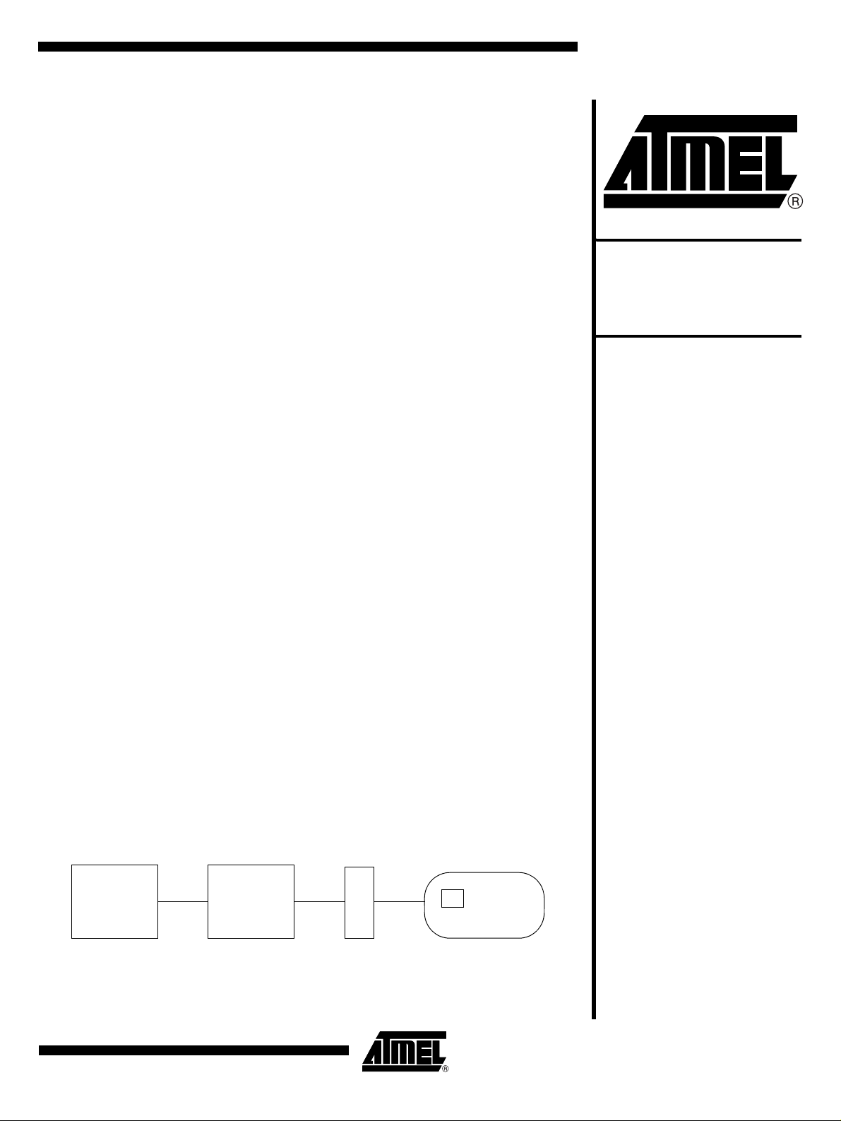
AT83C21GC is designed to simplify the integration of smart card interfaces in electronic devices.
It manages the electrical interface and communication with ISO 7816 –1/2/3/4 compatible smart cards and memory cards.
Figure 1. Basic Architecture of a Smart Card Reader
Host
Processor
AT83C21GC
Smart Card
Smart Card
Connector
This is a summary Document. A complete document is
available on the Gemplus Web site. www.gemplus.com
Page 2

The connection with the host processor is achieved via a serial asynchronous link; the rate can
be selected from a range from 1200 to 115,200 bps.
The software inside the GemCore chip handles a communication protocol with the host system
called the Gemplus Block Protocol (GBP).
A complete set of documentation is available on the Gemplus web site:
http://www.gemplus.com.
A GBP Interface Library Kit can be provided, upon request. It consists of the source code of the
GBP communication layer between the host and GemCore. It is written in the C language. See
the Gemplus developers’ site at www.gemplus.com. Enquiries can also be posted to
cardreader@atmel.com.
2
AT83C21GC
4247CS–SCR–11/05
Page 3

Ordering information
AT83C21GC
Part Number Temperature Range Package Packing
AT83C21GCxxx-ICSIL Industrial SSOP24 Stick
AT83C21GCxxx-ICRIL Industrial SSOP24 Tape & Reel
AT83C21GCxxx-ICSUL Industrial & Green SSOP24 Stick
AT83C21GCxxx-ICRUL Industrial & Green SSOP24 Tape & Reel
xxx : Firmware version
4247CS–SCR–11/05
3
Page 4

Pin Description Figure 2. 24-pin SSOP Pinout
Table 1. Port Signal Description
Internal
Signal
Port
Name
P1.0 CIO CV
P1.1 CC8 CV
Power
Supply ESD Type Description
CC
CC
4 kV I/O
4 kV I/O
CVSS
C
V
P1.5/CRST
P1.4/CCLK
P1.3/CC4
P1.2/CPRES
P1.1/CC8
P1.0/CIO
RST
XTAL2
XTAL1
LI
CC
1
2
3
4
5
6
7
8
9
10
11
12
SSOP24
24
V
CC
23
EVCC
22
D
V
21
VSS
P3.0/RxD
20
P3.1/TxD
19
P3.3/INT1/OE
18
P3.4/T0
17
P3.2/INT0
16
P3.5/CIO1/T1
15
14
P3.6/CCLK1/LED0
P3.7/CRST1/LED1
13
CC
Smart Card Interface Function
Card I/O – Pull-up medium is lower than 20KΩ
Smart Card Interface Function
Card contact 8 – Pull-up medium must be less than 20KΩ
P1.2 CPRES V
P1.3 CC4 CV
P1.4 CCLK CV
P1.5 CRST CV
P3.0 RxD EV
P3.1 TxD EV
P3.2 INT0 DV
P3.3 INT1 EV
P3.4 EV
P3.5 CIO1 DV
CC
CC
CC
CC
CC
CC
CC
CC
CC
CC
4 kV I
4 kV I/O
4 kV O
4 kV O
O
I/O
I/O
I/O
I/O
Smart Card Interface Function
Card presence
Smart Card Interface Function
Card contact 4 – Pull-up medium must be less than 20KΩ
Smart Card Interface Function
Card clock
Smart Card Interface Function
Card reset – Pull-up medium must be less than 20KΩ
UART Function
I
Receive data input
UART Function
Transmit data output.
Input/Output Function
P3.2 is a bi-directional I/O port with internal pull-ups.
Input/Output Function
P3.3 is a bi-directional I/O port with internal pull-ups.
Input/Output Function
P3.4 is a bi-directional I/O port with internal pull-ups.
Alternate Card Function
Card I/O: Pull-up medium must be less than 20K
4
AT83C21GC
4247CS–SCR–11/05
Page 5

Table 1. Port Signal Description (Continued)
Internal
Signal
Port
Name
P3.6 CCLK1 DV
Power
Supply ESD Type Description
CC
AT83C21GC
LED function
These pins can be directly connected to the cathode of the standard LED without
O
external current limiting resistors. The typical current of each output can be
programmed by software to 2, 4 or 10 mA (LEDCON register).
P3.7 CRST1 DV
RST V
CC
CC
Input/Output Function
I/O
P3.7 is a bi-directional I/O port with internal pull-ups.
I/O Reset Input
Holding this pin low for 64 oscillator periods while the oscillatoris running resets the
device. The Port pins are driven to their reset conditions when a voltage lower than V
is applied, whether or not the oscillator is running. This pin has an internal pull-up
resistor which allows the device to be reset by connecting a capacitor between this pin
and VSS. Asserting RST
the chip to normal operation. The output is active for at least 12 oscillator periods when
an internal reset occurs.
XTAL1 V
CC
I Input to the on-chip Inverting Oscillator Amplifier
To use the internal oscillator, a crystal/resonator circuit is connected
to this pin. If an external oscillator is used, its output is connected to this pin.
XTAL2 V
CC
O Output of the on-chip Inverting Oscillator Amplifier
To use the internal oscillator, a crystal/resonator circuit is connected
to this pin. If an external oscillator is used, XTAL2 may be left unconnected.
V
CC
PWR Supply Voltage
is used to power the internal voltage regulators and internal I/O’s.
V
CC
LI PWR DC/DC Input
LI must be tied to V
current for the pump charge of the DC/DC converter.
CV
CC
PWR Card Supply Voltage
is the programmable voltage output for the Card interface. It must be connected
CV
CC
to an external decoupling capacitor.
when the chip is in Idle mode or Power-down mode returns
through an external coil (typically 4, 7 μH) and provide the
CC
IL
DV
EV
CC
CC
V
CC
PWR Digital Supply Voltage
is used to supply the digital core and internal I/Os. It is internally connected to the
DV
CC
output of a 3V regulator and must be connected to an external decoupling capacitor.
PWR Extra Supply Voltage
is used to supply the level shifters of UART interface I/O pins. It must be
EV
CC
connected to an external decoupling capacitor. This reference voltage is generated
internally (automatically or not), or it can be connected to an external voltage
reference.
CVSS GND DC/DC Ground
CVSS is used to sink high shunt currents from the external coil.
VSS GND Ground
4247CS–SCR–11/05
5
Page 6

Atmel Corporation Atmel Operations
2325 Orchard Parkway
San Jose, CA 95131, USA
Tel: 1(408) 441-0311
Fax: 1(408) 487-2600
Regional Headquarters
Europe
Atmel Sarl
Route des Arsenaux 41
Case Postale 80
CH-1705 Fribourg
Switzerland
Tel: (41) 26-426-5555
Fax: (41) 26-426-5500
Asia
Room 1219
Chinachem Golden Plaza
77 Mody Road Tsimshatsui
East Kowloon
Hong Kong
Tel: (852) 2721-9778
Fax: (852) 2722-1369
Japan
9F, Tonetsu Shinkawa Bldg.
1-24-8 Shinkawa
Chuo-ku, Tokyo 104-0033
Japan
Tel: (81) 3-3523-3551
Fax: (81) 3-3523-7581
Memory
2325 Orchard Parkway
San Jose, CA 95131, USA
Tel: 1(408) 441-0311
Fax: 1(408) 436-4314
Microcontrollers
2325 Orchard Parkway
San Jose, CA 95131, USA
Tel: 1(408) 441-0311
Fax: 1(408) 436-4314
La Chantrerie
BP 70602
44306 Nantes Cedex 3, France
Tel: (33) 2-40-18-18-18
Fax: (33) 2-40-18-19-60
ASIC/ASSP/Smart Cards
Zone Industrielle
13106 Rousset Cedex, France
Tel: (33) 4-42-53-60-00
Fax: (33) 4-42-53-60-01
1150 East Cheyenne Mtn. Blvd.
Colorado Springs, CO 80906, USA
Tel: 1(719) 576-3300
Fax: 1(719) 540-1759
Scottish Enterprise Technology Park
Maxwell Building
East Kilbride G75 0QR, Scotland
Tel: (44) 1355-803-000
Fax: (44) 1355-242-743
RF/Automotive
Theresienstrasse 2
Postfach 3535
74025 Heilbronn, Germany
Tel: (49) 71-31-67-0
Fax: (49) 71-31-67-2340
1150 East Cheyenne Mtn. Blvd.
Colorado Springs, CO 80906, USA
Tel: 1(719) 576-3300
Fax: 1(719) 540-1759
Biometrics/Imaging/Hi-Rel MPU/
High Speed Converters/RF Datacom
Avenue de Rochepleine
BP 123
38521 Saint-Egreve Cedex, France
Tel: (33) 4-76-58-30-00
Fax: (33) 4-76-58-34-80
Literature Requests
www.atmel.com/literature
Disclaimer: The information in this docume nt is pro vided in connection with Atmel products. No license, express or imp lied, by estoppel or other wise,to anyintell ectualproperty right is granted by this document or in connection with the sale of Atmel products. EXC EPT AS SET FORTH IN ATMEL’S TERMS AND CONDI-TIONS OF
SALE LOCATED ON ATMEL’S WEB SITE, ATMEL ASSUMES NO LIABILITY WHATSOEVER AND DISCLAIMS ANY EXPRESS, IMPLIED OR STATUTORYWARRANTY RELATING TO ITS PRODUCTS INCLUDING, BUT NOT LIMITED TO, THE IMPLIED WARRANTY OF MERCHANTABILITY, FITNESS FOR A PARTICULARPURPOSE, OR NON-INFRINGEMENT. IN NO EVENT SHALL ATMEL BE LIABLE FOR ANY DIRECT, INDIRECT, CONSEQUENTIAL, PUNITIVE, SPECIAL
OR INCIDEN-TAL DAMAGES (INCLUDING, WITHOUT LIMITATION, DAMAGES FOR LOSS OF PROFITS, BUSINESS INTERRUPTION, OR LOSS OF INFORMATION) ARISING OUTOF THE USE OR INABILITY TO USE THIS DOCUMENT, EVEN IF ATMEL HAS BEEN ADVISED OF THE POSSIBILITY OF SUCH DAMAGES. Atmel makes norepresentationsor warrantie s with respect to the accuracy or completeness of the conten ts of this document and reserves the right to make
changes to specificationsand product descriptions at any time without notice. Atmel does not make any commitment to update the infor mation contained herein.
Unless specifically provided otherwise, Atmel products are not suitable for, and shall not be used in, automotive applications. Atmel’s products are not intended,
authorized, or warranted for useas components in applications intended to sup port or sustainlife.
© Atmel Corporation 200 5. All rights reserved. Atmel®, logo and combinations thereof, are registered trademarks, and Everywhere You Are
are the trademarks of Atmel Corporation or its subsidiaries. Other terms and product names may be trademarks of others.
Printed on recycled paper.
4247CS–SCR–11/05
SM
 Loading...