

Page 1

Features
• Thermal Sensitive Layer Over a 0.35 µm CMOS Array
• Image Zone: 0.4 x 11.6 mm
• Image Array: 8 × 232 = 1856 Pixels
• Pixel Pitch: 50 × 50 µm = 500 dpi Resolution
• On-chip 8-bit Analog to Digital Converter
• Serial Peripheral Interface (SPI) - 2 Modes:
– Fast Mode at 16 Mbps Max for Imaging
– Slow Mode at 200 kbps Max for Navigation and Control
• Die Size: 1.5 × 15 mm
• Operating Voltage: 2.3 to 3.6V
• I/O Voltage: 1.65 to 3.6V
• Operating Temperature Range: -40°C to 85°C
• Finger Sweeping Speed from 2 to 20 cm/Second
• Low Power: 4.5 mA (Image Acquisition), 1.5 mA (Navigation), <10 µA (Sleep Mode)
• Hard Protective Coating (>4 Million Sweeps)
• High Protection from Electrostatic Discharge
• Small Form Factor Packaging
FingerChip
®
Thermal
Fingerprint
Sweep Sensor,
Description
Atmel’s AT77C105A fingerprint sensor is dedicated to PDA, cellular and smartphone
applications. Based on FingerChip thermal technology, the AT77C105A is a linear
sensor that captures fingerprint images by sweeping the finger over the sensing area.
This product embeds true hardware-based 8-way navigation and click functions as
well, as enabling elimination of mechanical joystick devices.
Applications
• Scrolling, Menu and Item Selection for PDAs, Cellular or Smartphone Applications
• Cellular and Smartphones-based Security (Device Protection, Network and ISP
Access, E-commerce)
• Personal Digital Agenda (PDA) Access
• User Authentication for Private and Confidential Data Access
• Portable Fingerprint Acquisition
Chip-on-board Package
Hardware
Based
Navigation and
Click Functions,
Extended I/O
range (1.8-3.3V)
AT77C105A
Preliminary
Sweep your finger
to make life easier
Actual size of sensor
5419A–BIOM–01/05
Page 2

Table 1. Pin Description for Chip-on-board Package: AT77C105A-CB08V
Pin Number Name Type Description
1 Not connected
2 Not connected
3 Not connected
4 Not connected
5GNDDGDigital ground supply
6GNDAGAnalog ground supply - connect to GNDD
7 VDDD P Digital power supply
8VDDAPAnalog power supply - connect to V
9SCKI Serial Port Interface (SPI) clock
10 TESTA IO Reserved for the analog test, not connected
11 MOSI I Master-out slave-in data
12 VDD_IO P Input/output power supply - connect IO voltage compatibility accordingly
13 MISO O Master-in slave-out data
14 SCANEN I Reserved for the scan test in factory, must be grounded
15 SSS I Slow SPI slave select (active low
16 IRQ O Interrupt line to host (active low). Digital test pin
17 FSS I Fast SPI slave select (active low)
DD
18 RST I Reset and sleep mode control (active high)
19 FPL I Front plane, must be grounded
Note: The die attach is connected to pin 6 and must be grounded. The FPL pin must also be grounded.
2
AT77C105A [Preliminary]
5419A–BIOM–01/05
Page 3
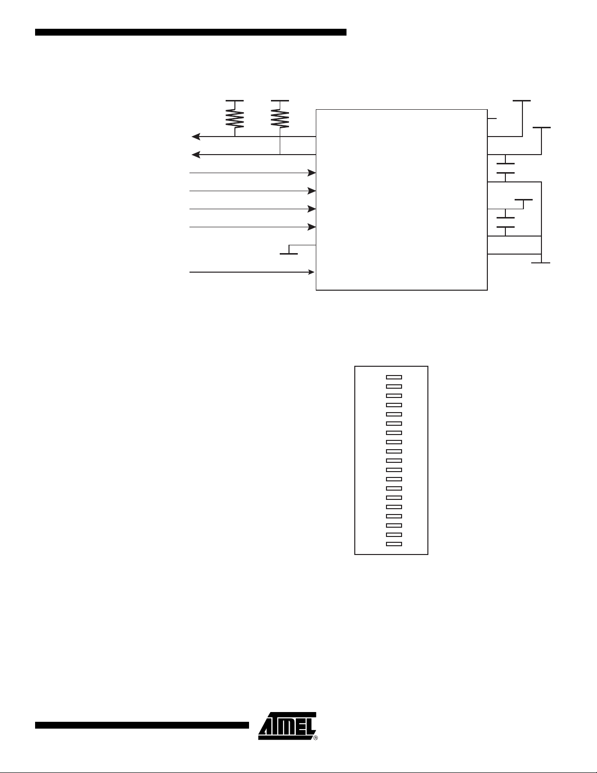
Figure 1. Typical Application
AT77C105A [Preliminary]
VDDD VDDD
10 kΩ
10 kΩ
TESTA
VDD_IO
NC
VDDD
IRQ VDD_IO
MISO VDDD
MOSI
SCK GNDD
10µ
VDDA
F
SSS VDDA
FSS
10µF
SCANEN GNDA
GND
RST
FPL
GND
The pull-up must be implemented for the master controller. The noise should be lower
than 30 mV peak to peak on VDDA.
Figure 2. Pin Description
NC
NC
NC
NC
GNDD
GNDA
VDDD
VDDA
SCK
TESTA
MOSI
VDD_IO
MISO
SCANEN
SSS
IRQ
FSS
RST
FPL
1
2
3
4
5
6
7
8
9
10
11
12
13
14
15
16
17
18
19
The TESTA pin is only used for testing and debugging. The SCANEN pin is not used in
the final application and must be connected to ground.
Warning: SSS and FSS must never be low at the same time. When both SSS and FSS
equal 0, the chip switches to scan test mode. With the SPI protocol, this
configuration is not possible as only one slave at a time can be selected.
However, this configuration works when debugging the system.
5419A–BIOM–01/05
3
Page 4

Specifications
Table 2. Absolute Maximum Ratings
Parameter Symbol Comments Value
Power supply voltage VDDD, VDDA -0.5 to 4.6V Note: Stresses beyond those listed
Front plane FPL GND to V
Digital input
Input/output pads power
supply
Storage temperature T
Lead temperature
(soldering 10 seconds)
SSS, FSS,
SCK, MOSI
GND to VDD +0.5V
VDD_IO GND to V
-50 to +95°C
T
stg
leads
Do not solder Forbidden
DD
DD
+0.5V
+0.5V
Table 3. Recommended Conditions of Use
Parameter Symbol Comments Min Typ Max Unit
Positive supply voltage V
DD
2.5 ±5%
3.3 ±1 0%
Front plane FPL Must be grounded GND V
Digital input voltage CMOS levels V
2.3
under “Absolute Maximum
Ratings” may cause permanent
damage to the device. These are
stress ratings only and functional
operation of the device at these or
any other conditions beyond those
indicated in the operational
sections of this specification is not
implied. Exposure to absolute
maximum rating conditions for
extended periods may affect device
reliability.
2.5
3.3
3.6 V
Digital output voltage CMOS levels V
Digital load C
Operating temperature range T
amb
L
Industrial “V” grade -40 to +85 °C
20 50 pF
Maximum current on VDDA IVDDA 0 - 60 mA
Table 4. Resistance
Parameter Min Value Standard Method
ESD
On pins HBM (Human Body Model) CMOS I/O 2 kV (TBC) MIL-STD-883 method 3015.7
On die surface (zap gun) air discharge
Mechanical Abrasion
Number of cycles without lubricant
Multiply by a factor of 20 for correlation with a real finger
Chemical Resistance
Cleaning agent, acid, grease, alcohol, diluted acetone 4 hours Internal method
±16 kV
(TBC)
NF EN 6100-4-2
200 000 MIL E 12397B
4
AT77C105A [Preliminary]
5419A–BIOM–01/05
Page 5

AT77C105A [Preliminary]
Note: TBC = To be confirmed
Table 5. Explanation of Test Levels
Level Description
I 100% production tested at +25°C
II 100% production tested at +25°C, and sample tested at specified temperatures (AC testing done on sample)
III Sample tested only
IV Parameter is guaranteed by design and/or characterization testing
V Parameter is a typical value only
VI 100% production tested at temperature extremes
D 100% probe tested on wafer at T
Table 6. Specifications
Parameter Symbol Test Level Min
= +25°C
amb
(1)
Typ Max
(1)
Unit
Resolution IV 50 Micron
Size IV 8 × 232 Pixel
Yield: number of bad pixels I 5 Bad pixels
Power Consumption and DC Characteristics
The following characteristics are applicable to the operating temperature -40°C ≤ T ≤ +85°C.
Typical conditions are: power supply = 3.3V; T
C
120 pF on digital outputs unless otherwise specified.
LOAD
Table 7. Power Requirements
Name Parameter Conditions Test Level Min
V
DD
I
DD
I
DDNAV
I
DDCLI
I
DDSLP
I
DDSTB
Positive supply voltage I 2.3 2.5/3.3 3.6 V
Current on VDD in acquisition mode I 3 4.5 6 mA
Current on VDD in navigation mode I 1 1.5 2 mA
Current on VDD in click mode I 0.2 0.3 0.5 mA
Current on VDD in sleep mode I 10 µA
Current on VDD in stand-by mode I Refer to “Power Management” on page 32
= 25°C; F
amb
= 12 MHz (1600 slices per second); duty cycle = 50%
SCK
(1)
Typ Max
(1)
Unit-
Note: 1. Min and max values are to be confirmed.
5419A–BIOM–01/05
5
Page 6

VDD_IO = 1.8V
Table 8. Digital Inputs
Logic Compatibility CMOS
Name Parameter Conditions Test Level Min Typ Max Unit
I
IL
I
IH
I
IOZ
V
V
V
IL
IH
HYST
Low level input current without pullup device
High level input current without
pull-down device
Tri-state output leakage without
pull-up/down device
Low level input voltage
High level input voltage
Schmitt trigger hysteresis
(1)
(1)
(1)
(1)
(1)
(1)
VI = 0V I 1 µA
VI = V
DD_IO
VI = 0V or V
DD_IO
I1µA
IV 1 µA
I
0.15
V
DD_IO
DD
(1)
I0.6 V
IV
V
V
0.4
DD_IO
0.3
DD_IO
(1)
Table 9. Digital Outputs
Logic Compatibility CMOS
Name Parameter Conditions Test Level Min Typ Max Unit
= 4 mA
I
V
OL
V
OH
Low level output voltage
High level output voltage
OL
V
= 1.8V ±8%
DD
I
= -4 mA
OH
V
= 3.3V ±10%
DD
I
I0.85 V
DD
V
DD_IO
0.15
(1)
V
V
V
V
V
Note: 1. A minimum noise margin of 0.05 VDD should be taken for Schmitt trigger input threshold switching levels compared to V
and VIH values.
IL
6
AT77C105A [Preliminary]
5419A–BIOM–01/05
Page 7

AT77C105A [Preliminary]
VDD_IO = 2.3V to 3.6V
Table 10. Digital Inputs
Logic Compatibility CMOS
Name Parameter Conditions Test Level Min Typ Max Unit
I
IL
I
IH
I
IOZ
V
V
V
IL
IH
HYST
Low level input current without pullup device
High level input current without
pull-down device
Tri-state output leakage without
pull-up/down device
Low level input voltage
High level input voltage
Schmitt trigger hysteresis
(1)
(1)
(1)
(1)
(1)
(1)
VI = 0V I 1 µA
VI = V
DD_IO
VI = 0V or V
DD_IO
I1µA
IV 1 µA
V
V
0.5
DD_IO
0.09
DD_IO
IV
I
I
V
0.6
DD_IO
(1)
0.06
V
DD_IO
(1)
Table 11. Digital Outputs
Logic Compatibility CMOS
Name Parameter Conditions Test Level Min Typ Max Unit
I
= 4 mA
V
OL
Low level output voltage
V
DD _IO
OL
= 2.3V to
I
3.6V
I
= -4 mA
V
OH
High level output voltage
V
DD_IO
OH
= 2.3V to
I0.90 V
DD
3.6V
V
DD_IO
0.10
(1)
V
V
V
V
V
Input/Output Voltage Level Compatibility
The I/O voltage level compatibility is set by the power voltage driven on the VDD_IO
pad. For 1.8V level compatibility, connect VDD_IO to a 1.8V power supply.
5419A–BIOM–01/05
7
Page 8

Switching Performances
The following characteristics are applicable to the operating temperature -40°C ≤ T ≤ +85°C.
Typical conditions are: nominal value; T
specified otherwise.
Table 12. Timings
Parameter Symbol Test Level Min Typ Max Unit
Clock frequency acquisition
mode
Clock frequency navigation
mode and chip control
Duty cycle (clock SCK) DC IV 20 50 80 %
Reset setup time T
Slave select setup time T
Slave select hold time T
Note: 1. T
SCK
= 1/F
(clock period)
CTRL
Table 13. 3.3V ±10% Power Supply
Parameter Symbol Test Level Min Typ Max Unit
Data in setup time T
Data in hold time T
Data out valid T
Data out disable time from SS
high
IRQ hold time T
Note: All power supplies = +3.3V
amb
F
ACQ
F
CTRL
RSTSU
SSSU
SSHD
SU
T
DIS
IRQ
H
V
= 25°C; F
= 12 MHz; duty cycle = 50%; C
SCK
120 pF in digital output unless
LOAD
IV 8 16 MHz
I- 0.2MHz
I½ T
I½ T
I½ T
SCK
SCK
SCK
(1)
(1)
(1)
IV 3 ns
IV 1 ns
I30ns
IV 3.8 ns
IV 3 µs
ns
ns
ns
Table 14. 2.5V ±5% Power Supply
Parameter Symbol Test Level Min Typ Max Unit
Data in setup time T
Data in hold time T
Data out valid T
Data out disable time from SS
high
IRQ hold time T
Note: All power supplies = +2.5V
8
AT77C105A [Preliminary]
SU
H
V
T
DIS
IRQ
IV 3 ns
IV 1 ns
I30ns
IV 3.8 ns
IV 3 µs
5419A–BIOM–01/05
Page 9

AT77C105A [Preliminary]
Table 15. 1.8V ±5% Power Supply
Parameter Symbol Test Level Min Typ Max Unit
Data in setup time T
Data in hold time T
Data out valid T
Data out disable time from SS
high
IRQ hold time T
SU
H
V
T
DIS
IRQ
ns
ns
ns
ns
µs
5419A–BIOM–01/05
9
Page 10
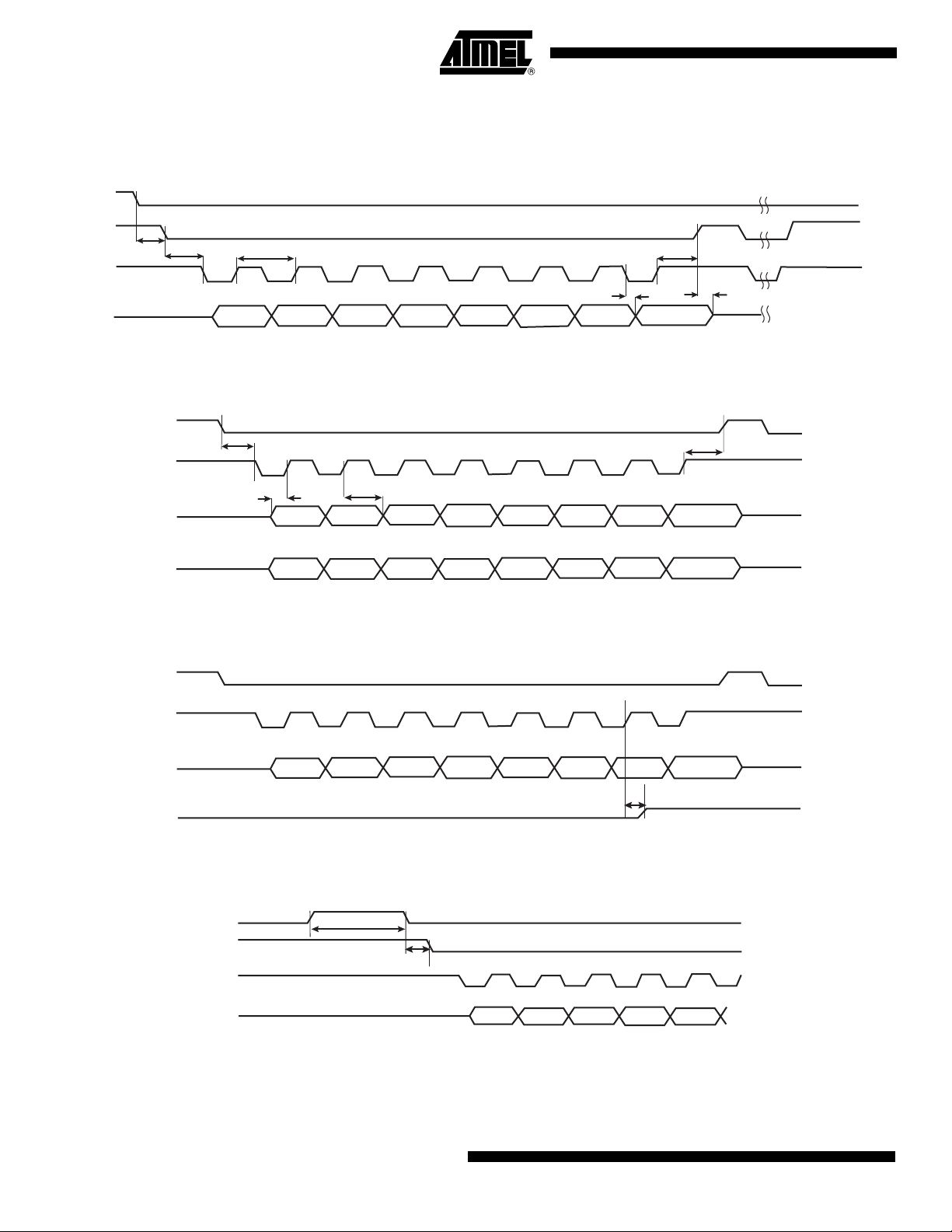
Timing Diagrams: Slow and Fast SPI Interface
Figure 3. Read Timing Fast SPI Slave Mode
RST
SS
T
T
sssu
rstsu
SCK
MISO
Figure 4. Read/Write Timing Slow SPI Slave Mode
SS
SCK
T
DC
sssu
T
T
sshd
T
v
dis
T
sshd
MOSI
MISO
T
su
Th
Figure 5. Read Status Register to Release IRQ
SS
SCK
MOSI
IRQ
11 0 0 0 X
Figure 6. Chip Initialization
RST
SS
SCK
Min = 10 µs
T
rstsu
0X
T
irq
10
MISO
AT77C105A [Preliminary]
5419A–BIOM–01/05
Page 11

Functional Description
AT77C105A [Preliminary]
The AT77C105A is a fingerprint sensor based on FingerChip technology. It is controlled
by an SPI serial interface through which output data is also transferred (a slow SPI for
the pointing function and a fast one for acquisition). Six modes are implemented:
– Sleep Mode: A very low consumption mode controlled by the reset pin RST.
In this mode, the internal clocks are disabled and the registers are initialized.
– Stand-by Mode: Also a low consumption mode that waits for an action from
the host. The slow serial port interface (SSPI) and control blocks are
activated. In this mode the oscillator can remain active.
– Click Mode: Waits for a finger on the sensor. The SSPI and control blocks
are activated. The local oscillator, the click array and the click block are all
activated.
– Navigation Mode: Calculates the finger’s x and y movements across the
sensor. The SSPI and control blocks are still activated. The local oscillator,
the navigation array and the navigation block are also activated.
– Acquisition Mode: Slices are sent to the host for finger reconstruction and
identification. The SSPI and control blocks are still activated. The fast serial
port interface block (FSPI) and the acquisition array are activated, as well as
the local oscillator when watchdog is required.
– Test: This mode is reserved for factory testing.
In the final application, three main modes are used:
– Stand-by: Low consumption mode
– Pointing: Equivalent to click and navigation modes
– Acquisition: Fingerprint image capture
Note: The term”host” describes the processor (controller, DSP...) linked to the sensor. It is the
master. In the description of n-bit registers (see “Function Registers” on page 13), the
term “b0” describes the Least Significant Bit (LSB). The term “b(n-1)” describes the Most
Significant Bit (MSB). Binary data is written as 0b_ and hexadecimal data as 0x_.
5419A–BIOM–01/05
11
Page 12
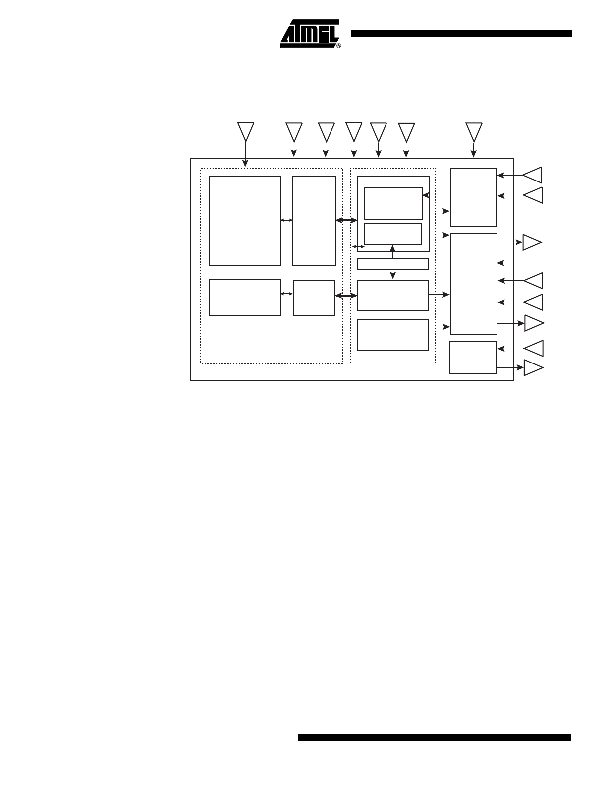
Sensor and Block Diagram
Figure 7. Functional Block Diagram
FPL VDDA GNDA VDDD
Pixel Array
(232 x 8)
Array
CTRL
GNDD RST
VDD_IO
Fast Serial
Interface
Acquisition
Navigation
Algorithms
SPI
(8-16 MHz)
FSS
SCK
MISO
Oscillator (420 kHz)
Click Pixels
(12)
Click
CTRL
Click
Algorithm
Watchdog
Heating
The circuit is divided into the following main sections:
• An array or frame of 8 × 232 pixels + 1 dummy column
• An analog to digital converter
• An on-chip oscillator
• Control and status registers
• Navigation and click units
• Slow and fast serial interfaces
Slow Serial
Interface
SPI
(200 kHz)
+
Control
Register
Test
MOSI
SSS
IRQ
SCANEN
TESTA
12
AT77C105A [Preliminary]
5419A–BIOM–01/05
Page 13

Function Registers
AT77C105A [Preliminary]
Table 16. Registers
Register Address (b3 down to b0) Read/Write
STATUS 0000 Read
MODECTRL 0001 Read/Write
ENCTRL 0010 Read/Write
HEATCTRL 0011 Read/Write
NAVCTRL 0100 Read/Write
CLICKCTRL 0101 Read/Write
MOVCTRL 0110 Read/Write
0111 Reserved
NAVIGATION
NAVIGATION
NAVIGATION
PIXELCLICK 1011 Reserved
PIXELCLICK 1100 Reserved
(1)
(1)
(1)
1000 Read
1001 Reserved
1010 Reserved
PIXELCLICK 1101 Reserved
1110 Reserved
Note: 1. Navigation requires 3 registers. The reading of the first register (0b1000) enables the
reading of all 3 registers.
5419A–BIOM–01/05
13
Page 14

Status Register Register Name: Status (8 bits)
Access Type: Read Only
Function: State of AT77C105A
b7 b6 b5 b4 b3 b2 b1 b0
CLICK MOV
00000000
TRANSIT
• CLICK: Click detection
0: default
1: click detected
• MOV: Movement detection
0: default
1: X or Y movement detected
• TRANSIT: Not used, for testing only
•SLICE: Not used, for testing only
• READERR: Read error detection
0: default, no error
1: read error detected
Note: To clear the interrupts, the status register is initialized after each reading from the host.
SLICE READERR – – –
14
AT77C105A [Preliminary]
5419A–BIOM–01/05
Page 15

AT77C105A [Preliminary]
Modectrl Register Register Name: Modectrl (7 bits)
Access Type: Read/Write
Function: Mode control
b6 b5 b4 b3 b2 b1 b0
MODE (MSB) MODE MODE MODE (LSB) ANALOGRST – –
0000100
• MODE: Select operating mode
0000: standby
0001: test (reserved for factory use)
0010: click
0100: navigation
1000: acquisition
Certain changes can be made. For example, MODE can be set to 0b0110 to activate
click and navigation.
• ANALOGRST: Reset local oscillator
0: oscillator in active mode
1: oscillator in power-down mode
Notes: 1. Click or navigation modes cannot be used when the local oscillator is switched off..
2. To return to standby mode and stop the oscillator (to save on power consumption),
two Modectrl register accesses are necessary: the first one to select standby mode
and the second to switch off the oscillator.
3. The read-only registers cannot be read when the oscillator is turned off.
4. To shift between navigation and acquisition modes, you must be in standby mode
(Modectrl = 0b00001).
If modes such as “acquisition and click” or “acquisition and navigation” are programmed
together, they will be ignored by the system.
Programmed Mode Register Value
11xx 01xx
1x1x 0x1x
With x = 0 or 1.
5419A–BIOM–01/05
15
Page 16

Enctrl Register Register Name: Enctrl (7 bits)
Access Type: Read/Write
Function: Interrupts control
b6 b5 b4 b3 b2 b1 b0
CLICKEN MOVEN TRANSITEN SLICEN READERREN – –
0000000
• CLICKEN: Click interrupts enable
0: default
1: click IRQ enabled
IRQ is generated when a click is detected.
• MOVEN: Movement interrupts enable
0: default
1: movement IRQ enabled
IRQ is generated when an X or Y movement is detected.
• TRANSITEN: Not used, for testing only
• SLICEN: Not used, for testing only
• READERREN: Read error interrupts enable
0: default
1: read error IRQ enabled
IRQ is generated when a read error is detected.
Note: The interrupt is cleared after the status register is read.
Heatctrl Register Register Name: Heatctrl (7 bits)
Access Type: Read/Write
Function: Heating control
b6 b5 b4 b3 b2 b1 b0
HEAT WDOGEN HEATV (MSB) HEATV(LSB) – – –
0000000
• HEAT: Sensor heating
0: default, no heating
1: heating
The default value is recommended to optimize power consumption.
• WDOGEN: Watchdog enable
0: default
16
AT77C105A [Preliminary]
5419A–BIOM–01/05
Page 17

1: watchdog enabled
Watchdog automatically stops heating of the sensor after a time-out.
• HEATV (2 bits): Heating power value
00: 50 mW
01: 100 mW
10: reserved
11: reserved
V
is between 2.5 and 3.6V.
DD
Notes: 1. Heating can only be used in the acquisition mode (it is not allowed in navigation or
click modes).
2. The oscillator has to be activated when the watchdog is required and must not be
stopped while the watchdog remains active.
Navctrl Register Register Name: Navctrl (7 bits)
Access Type: Read/Write
Function: Navigation control
AT77C105A [Preliminary]
b6 b5 b4 b3 b2 b1 b0
NAVFREQ
(MSB)
1000000
NAVFREQ (LSB) NAVV ( MSB) NAVV (LSB) CLICKV (MSB) CLICKV (LSB) reserved
• NAVFREQ: Navigation frequency
00: 5.8 kHz
01: 2.9 kHz (default value)
10: 1.9 kHz
11: 1.5 kHz
A faster frequency enables faster finger movement detection. A lower frequency
enhances sensitivity. Refer to Notes 1 and 2 on page 18.
• NAVV: Navigation pixels threshold
00: lower threshold
01:
10:
11: higher threshold
Sets the minimum analog value detected as a high level (‘1’). Refer to Note 1 on page
18.
5419A–BIOM–01/05
• CLICKV: Click pixels threshold
00: lower threshold
01:
10:
11: higher threshold
17
Page 18

Sets the minimum analog value detected as a high level (‘1’) and the maximum analog
value detected as a low level (‘0’). See Note 3 on page 18.
Notes: 1. Navfreq and Navv registers should not be changed once the navigation mode is
selected. Finger sensitivity refers to the minimum level of information required from a
finger. The sensitivity is linked to the integration time; a longer integration time
enables better sensitivity but does not tolerate fast movement.
2. The navigation frequency is the frequency needed for the reading of one new navigation frame.
3. The Clickv register should not be changed once the click mode is selected.
Clickctrl Register Register Name: Clickctrl (7 bits)
Access Type: Read/Write
Function: Click control
b6 b5 b4 b3 b2 b1 b0
CLICKFREQ
(MSB)
0101101
CLICKFREQ
(LSB)
CLICKDET
(MSB)
CLICKDET
(LSB)
CLICKCPT
(MSB)
CLICKCPT CLICKCPT
(LSB)
• CLICKFREQ: Click pixels reading frequency
00: 180 Hz
01: 90 Hz (default value)
10: 60 Hz
11: 45 Hz
Faster frequency enables faster finger click detection. Lower frequency enables higher
sensitivity.
• CLICKDET: Threshold for selecting the black/white color of a slice
00: more than 7 black/white pixels and less than 5 white/black pixels
01: more than 8 black/white pixels and less than 4 white/black pixels
10: more than 9 black/white pixels and less than 3 white/black pixels
11: more than 10 black/white pixels and less than 2 white/black pixels
• CLICKCPT: Click detection counter (maximum number of slices read between two
transitions)
000: 5
001: 7
010: 10
011: 12
100: 16
101: 20
110: 25
111: 31
18
AT77C105A [Preliminary]
5419A–BIOM–01/05
Page 19

Two transitions are interpreted as a click if the number of slices between them is less
than CLICKCPT. This is used to differentiate a touch-down/touch-up from a real click. A
click is equivalent to two close touch-down/touch-up transitions.
This register adjusts the “time out” for considering the two transitions as a click.
Note: Clickfreq and Clickcpt registers should not be changed once the click mode is selected.
Movectrl Register Register Name: Movctrl (7 bits)
Access Type: Read/Write
Function: In stream mode, during navigation calculation, the AT77C105A must
interrupt the host when a maximum absolute X or Y movement is detected (second and
third navigation registers). The MOVECTRL register enables you to control this value.
This value can be set as the minimum finger movement value at which the pointing
device makes a displacement.
AT77C105A [Preliminary]
b6 b5 b4 b3 b2 b1 b0
(MSB) – – – – – (LSB)
0000000
• MOVCTRL: Generates an interrupt when the second or third navigation register (X
or Y absolute movement) is greater than the value programmed in the Movectrl
register
0b0000000
0b0000001
0b0000010
...
0b1111111
For example, when MOVCTRL = 0b0001001, an interruption to the host is generated
when the absolute X movement register (second navigation register) or absolute Y
movement register (third navigation register) is greater than 0b00010010.
Note: The Movctrl register should not be changed once the navigation mode is selected.
5419A–BIOM–01/05
19
Page 20

Navigation Register
Register Name: Navigation (3 x 8 bits)
Access Type: Read Only
ing command of the first navigation register [address 0b1000] returns the value of the
three registers).
Function: The format of the navigation registers is similar to the PS/2 protocol. Three
registers are used to codemovements and clicks. The navigation registers are initialized
after each reading. The registers only represent actions (movement, click, transition...)
that have occurred since the last data packet sent to thehost.
General Register
b7 b6 b5 b4 b3 b2 b1 b0
YOV R XOVR YSIGN XSIGN 1 TRANS CLICK FINGER
0 0 0 0 1 0 0 0
• YOVR: Y overflow
0: default
1: Y movement overflow
High (‘1’) when the Y movement counter is overflowed.
• XOVR: X overflow
0: default
1: X movement overflow
(these three registers cannot be read individually. The read-
High (‘1’) when the X movement counter is overflowed.
• YSIGN: Y sign bit
0: default, positive Y movement
1: negative Y movement
High (‘1’) when the Y movement is negative. Low when the Y movement is positive.
• XSIGN: X sign bit
0: default, positive X movement
1: negative X movement
High (‘1’) when the X movement is negative. Low when the X movement is positive.
• TRANS: Not used, for test purposes only.
• CLICK: Click
0: default
1: click detected
This function is not in the PS/2 protocol.
• FINGER: Not used, for test purposes only.
20
AT77C105A [Preliminary]
5419A–BIOM–01/05
Page 21

AT77C105A [Preliminary]
Note: In the PS/2 protocol, bits b2 and b1 are used to code the middle and right buttons
respectively, and b3 is set to high.
Absolute X Movement Register (0 to 255 Pixels)
b7 b6 b5 b4 b3 b2 b1 b0
XMOV (MSB)––––––XMOV (LSB)
00000000
Absolute Y Movement Register (0 to 255 Pixels)
b7 b6 b5 b4 b3 b2 b1 b0
YMOV (MSB)––––––YMOV (LSB)
00000000
Note: When a click is detected, the information is placed in the b7 bit of the status register and
in the b1 bit of the general navigation register. The reading of the status register initializes the b7 bit but does not initialize the b1 bit of the general navigation register. The host
must carefully correlate the two bits.
5419A–BIOM–01/05
21
Page 22

SPI Interface General Description
Two communication busses are implemented in the device:
• The control interface, a slow bus that controls and reads the internal registers
(status, navigation, control...).
• The pixels’ acquisition interface, a fast bus that enables full pixel acquisition by the
host.
A synchronous Serial Port Interface (SPI) has been adopted for the two communication
busses.
The SPI protocol is a slave/master fullduplex synchronous serial communication. This
protocol uses three communication signals:
• SCK (Serial Clock): the communication clock
• MOSI (Master Out Slave In): the data line from the master to the slave
• MISO (Master In Slave Out): the data line from the slave to the master
The slaves are selected by an input pin SS/ (Slave Select). A master can communicate
with several slaves.
The word length of the transferred data is fixed to 8 bits. The Most Significant Bit (MSB)
is sent first. For each 8-bit transfer, 8 bits are sent from the master to the slave and 8
bits transferred from the slave to the master. Transfers are still synchronized with the
communication clock (SCK). Only the host can initialize transfers. To send data, the
slave must wait for an access from the master. When there is no transfer, a clock is not
generated.
Figure 8. One Master with Several Slaves
SS/3
Slave #3
SCK
MISO
MOSI
Master
SS/1
Slave #1
SS/2
Slave #2
When a master is connected with several slaves, the signals SCK, MISO and MOSI are
interconnected. Each slave SS is driven separately. Only one slave can be selected, the
others have their MISO tri-stated and ignore MOSI data.
The SS/ signal falls a half-period before the first clock edge, and rises a half-period after
the last clock edge.
Clock Phase and Polarity During phase zero of the operation, the output data changes on the clock’s falling edge
and the input data is shifted in on the clock’s rising edge. In phase one of the operation,
the output data changes on the clock’s rising edge and is shifted in on the clock’s falling
edge.
22
AT77C105A [Preliminary]
5419A–BIOM–01/05
Page 23

AT77C105A [Preliminary]
Polarity configures the clock’s idle level, which is high (“1”) during polarity one of the
operation and low (
AT77C105A and the SPI The AT77C105A is always the slave and the host always the master. The host drives
the SCK clock. Both the AT77C105A and the host transmit data with the MISO signal.
The word length of the transferred data is fixed to 8 bits. The Most Significant Bit (MSB)
is sent first.
The AT77C105A supports only one phase and polarity configuration:
• The clock’s idle level set to high (polarity 1)
• The output data changed on the clock’s falling edge, and input data shifted in on the
clock’s rising edge (phase 0).
Figure 9. SPI Waveform (Phase = 0, Polarity = 1)
SCK
“0”) during polarity zero of the operation.
MOSI/MISO
Note: During initialization of the SCK wire (power-on or reset), SS/ has to be inactive (“1“).
SS/
Emission
MSB
Reception
LSB
Recommendations The SSS or FSS falling edge should be half a clock cycle before the first SCK falling
edge and the SSS or FSS rising edge should be half a clock cycle after the last SCK
rising edge.
SPI Behavior with Hazardous Access
The control register block uses an internal finite state machine that can only be initialized by the RST pin (asynchronous reset). When SPI access does not use 8 clock
pulses, the internal finite state machine is desynchronized. The only way to resynchronize it is by resetting the sensor with the RST pin. No requester modification is recorded
when a write access is made on a read-only register. Reliable initialization of read-only
registers is not guaranteed when the slow SPI’s maximum clock frequency is not
respected.
5419A–BIOM–01/05
23
Page 24

Control Interface (Slow SPI)
This interface controls the sensor’s internal registers. The protocol enables reading and
writing of these registers.
The master (host) initiates transfers to the slave (sensor). The sensor can only use its
interrupt pin to communicate with the host. When the host is interrupted, it must read the
status register before continuing operation.
The word length of the transferred data is fixed to 8 bits. The Most Significant Bit (MSB)
is sent first.
Communication Protocol Accesses to the host are structured in packets of words. The first word is the command
and the other words are the data.
The b7 bit is used to differentiate the command and data. When the word is a command,
b7 is high (
The following protocol is used:
Command Format The host indicates to the sensor if it wants to read or write into a register and indicates
the register’s address.
b7 b6 b5 b4 b3 b2 b1 b0
“1”) and when the word is a piece of data, b7 is low (“0”).
1
Data Format (Writing into
Read
(1)/Write (0)
Address (b3) Address (b2) Address (b1) Address (b0) x x
If writing into a register, the host transmits the data.
Register)
b7 b6 b5 b4 b3 b2 b1 b0
0 Data (b6) Data (b5) Data (b4) Data (b3) Data (b2) Data (b1) Data (b0)
Data Format (Reading of Register)
If reading a register, the host transmits one or several packets of data and data is shifted
in from the sensor. The host transmits dummy words with the data format (b7 is low
[
“0”]). If reading the navigation or click pixel registers, the host transmits three packets of
data to read the three registers.
b7 b6 b5 b4 b3 b2 b1 b0
0xxxxxxx
Note: The host cannot communicate with the sensor without receiving data from it. Useless data is ignored by the host.
24
AT77C105A [Preliminary]
5419A–BIOM–01/05
Page 25

AT77C105A [Preliminary]
Communication Speed To reduce consumption, the control interface’s communication speed is set to the lowest
possible speed and depends on the host’s configuration.
To communicate with “fast” controllers, the sensor’s communication speed can be set to
200 kbits/s.
Example for the MODECTRL Register
Figure 10 represents a typical writing sequence into an internal register (MODECTRL
register in this example).
See Appendix B for flowchart.
Figure 10. Writing into an Internal Register
SSS
SCK
MOSI
10000 xx1
MISO
xx x xxxx x
Writing into MODECTRL Register Requested
Note: The break on SCK on the SPI chronogram has been added for better comprehension only. In a real application, SCK can be
continuous.
00110000
xx x xxxx x
New Data to be Written into MODECTRL Register
(Navigation and Click Mode)
Figure 11 represents a typical reading sequence of a register different from the navigation register. In this example, the status register is used.
Figure 11. Reading Sequence of a Register (Except for Navigation Registers)
SCK
MOSI
MISO
11000 xx0
xx x xxxx x
Reading of STATUS Register Requested
0xxxxxx
10 0 0000 0
x
Emission of the STATUS Register
(Click Detected)
5419A–BIOM–01/05
25
Page 26

Example of Navigation Registers
Figure 12 represents a typical reading sequence of the three navigation registers.
Refer to “Appendix C” on page 37 for flowchart
Figure 12. Reading of the Navigation Registers
SCK
MOSI
MISO
1
X
0 0 0 X X
X X
Reading of Navigation
Register Requested
X X X X
X
0
0 1 0
0 0 0
(No Overflow, Y Negative Movement
Click Detected, Black Slice)
Image Capture (Fast SPI)
This serial interface enables full-speed acquisition of the sensor’s pixels by the host.
This interface only supports the serial clock (SCK) and one data line: MISO (Master In/
Slave Out).
X
X XX
0 1 0
Emission of the First
Navigation Register
0
X
X
Emission of the Second
Navigation Register
(X Absolute Movement
X X X X
1 0 0 00
= 24 Pixels)
X X XX X X
X
0
0 0 1 0 0 0 0
1
Emission of the Third
Navigation Register
(Y Absolute Movement
= 144 Pixels)
Communication Protocol When the sensor is in acquisition mode, the host can receive pixels through the fast SPI
(FSS/ = 0). The host must transmit the communication clock (SCK) to receive the pixels.
This clock must have a regular frequency to obtain constant fingerprint slices (See “Registration Integration Time” on page 30.).
With the sensor configured to acquisition mode, the controller can proceed to fast
accesses.
26
AT77C105A [Preliminary]
5419A–BIOM–01/05
Page 27

Figure 13. Example of an 8-bit Access
Sensor
Sending of 2 Pixels (8 Bits)
AT77C105A [Preliminary]
Controller
FSS/ = 0
Sending of Dummy Data
0b0000000
Reception of 2 Pixels
End of
Communication
?
Yes
FSS/ = 1
No
During an 8-bit access, the sensor transmits two pixels (each pixel is coded on 4 bits).
Figure 14. Fast SPI Communication
SCK (Pixel Clock)
MISO
Transmission Clock
Edge (Sensor)
Bit3
MSB
Bit2
Pixel 2i
Bit0 Bit3 Bit2 Bit1 Bit0 Bit2 Bit1 Bit0
Bit1
Pixel 2i - 1
Reception Clock
Edge (Host)
Bit3
MSB
Pixel 2i + 2 Pixel 2i + 1
Bit3 Bit2 Bit1 Bit0
Communication Speed The acquisition speed of the pixels is linked to the clock’s communication speed. The
faster the communication clock, the faster the authorized maximum finger sweeping
speed. The sensor supports fast communications up to 16 Mbps.
Reading of Frame A frame consists of 232 true columns and 1 dummy column of 8 pixels of 4 bits each. A
frame starts with a dummy column.
Figure 15. Example of a Frame
Dummy
Synchro = F0F00200
5419A–BIOM–01/05
Column
0
F
0
F
2
0
0
0
p1
p2
p3
p4
p5
p6
p7
p8
P9
p10
p11
P12
P13
P14
P15
p16
232 x 8 Pixels Column
Pixel Frame
27
Page 28

Figure 16. Reading of Frame
SCK
MISO
F 0 F 0 20 0 P2 P1 P4 P6 P3 P5 P8 P7
The first dummy column, at the beginning of the pixel array, is added to the sensor to act
as a specific easy-to-detect pattern, and represents the start of the frame tag.
The pixel array is always read in the following order: the first byte, following the 4 bytes
of the dummy column, which contains the value of the pixels physically located on the
upper left corner of the array, when looking at the die with bond pads to the right. Then
another 4 bytes are read that contain the value of the pixels located in the same column
from top to bottom. The next column on the right is output, and so on, until the last line
on the right, close to the bond pads, is output.
Even values are first sent during the data serialization for SPI transfer. Therefore, the
synchronization sequence on the chip’s MISO output is F0F00200.
0 P10 P9
Dummy Column
Notes: 1. For the first array or frame reading, 40 dummy clock cycles must be sent before the first data arrives. This is necessary for
the initialization of the chip pipeline. Consequently, the first synchronization sequences appear after 40 clock cycles. For the
following array readings, data arrives at each clock cycle. One should implement a synchronization routine in the protocol to
look for the F0F00200 pattern.
2. The Most Significant Bit (MSB) is sent first.
First Pixel
Column
Second Pixel
Column
Reading of Entire Image The FingerChip delivers fingerprint slices or frames with a height of 0.4 mm and a width
of 11.6 mm (this equals 8 × 232 pixels). Pixels are sampled/read sequentially and are
synchronous with SCK. Raw slices are captured by the acquisition system and overlapped with the corresponding X or Y finger displacement computed by Atmel
reconstruction software. This reconstruction software supports a sweeping speed from 2
to 20 cm/s.
The table below shows finger speeds according to the different clock frequencies. The
reconstruction results are obtained after acquisition of all slices.
Table 17. Finger Speeds Versus Clock Frequencies
Absolute
Fsck
(MHz)
1 1 134 3 Too slow
2 2 268 6 Too slow
Data Rate
(Mbit/s)
Slice Rate
(Slices/s)
Maximum Finger
Speed (cm/s) Comments
28
4 4 536 12 Minimum
6 6 804 18 Normal speed
AT77C105A [Preliminary]
5419A–BIOM–01/05
Page 29

AT77C105A [Preliminary]
Table 17. Finger Speeds Versus Clock Frequencies
Absolute
Fsck
(MHz)
8 8 1072 24 Good speed
12 12 1608 36 Very good speed
16 16 2146 48 Very good speed
Data Rate
(Mbit/s)
Slice Rate
(Slices/s)
Maximum Finger
Speed (cm/s) Comments
5419A–BIOM–01/05
29
Page 30

Registration Integration Time
The pixel’s integration time (the time needed for one frame reading) must be as regular
as possible to obtain consistent fingerprint slices. This time is directly dependant on the
SCK, SPI clock and frequency. Therefore, the SPI cycle of 4 × 8 × 233 clock pulses
should be as regular as possible.µ
Figure 17. Regular Integration Time
Frame n
Clock SCK
4 x 8 x 233 =
7456 Pulses
Note: The 500 µs duration corresponds to the host’s computation time (slice reconstruction, finger detection…) and in the illustration is
given as an example only. Once the host detects a finger, this value remains constant, thus guaranteeing a regular integration
time.
500 µs max
233 = 232 + 1 Dummy Column
7456 Pulses
Regular Integration Time
Frame n+1
Frame n+2
7456 Pulses
Frame n+3
7456 pulses
Navigation (Slow SPI)
The sensor’s navigation function includes the processing elements necessary for providing the displacement of the finger touching the sensor in an up or down and right or
left direction. It is aimed at a screen menu navigation or simple pointing application. In
addition, a click processing function is embedded to detect a quick touch of the finger on
the sensor. It is aimed at screen text, box or object selection. A double-click function
could also be implemented in the software.
This interface has been designed to resemble the PS/2 mouse protocol.
30
An interrupt signal IRQ indicates to the host that an action has been detected. The host
must read the status register to obtain details on the action. The IRQ signal enables
implementation of an efficient power consumption protocol.
Note:
• Click and navigation modes can be used together.
• Two configurations are implemented for the click and navigation modes:
– Stream mode, where the sensor sends an interrupt to the host when a
movement or a change in the button’s state is detected.
– Remote mode, where the sensor does not interrupt the host but waits for its
registers to be read.
In these two modes, the registers are initialized after each reading from the host.
See “Appendix D” on page 38. for an example of an interrupt generated by a movement
detection.
AT77C105A [Preliminary]
5419A–BIOM–01/05
Page 31

Navigation See “Navigation Register” on page 20.
The typical navigation slice frequency has been fixed to 2.9 kHz. A programmable
divider is implemented in the control registers (NAVFREQ) to reduce this frequency.
Finger displacement is provided as a number of pixels in X and Y directions. Negative
movements are possible. The register is cleared after the navigation registers are read.
These registers are incremented or decremented between two accesses.
Table 18.
AT77C105A [Preliminary]
Navctrl
Register
(Bits b6 to b5)
00 5.8 172 30
01 2.9 345 15
10 1.9 526 9.5
11 1.5 666 7.5
Typical Navigation
Slice Frequency
(kHz)
Typical
Integration Time
(µs)
Typical Maximum
Finger Speed
(cm/s)
Click See “Clickctrl Register” on page 18.
The sensor generates a click detection. The host must read the b7 bit of the status register or the b1 bit of the general navigation register.
The click function is composed of an array of a few pixels and a processing unit. The
typical click slice frequency is 90 Hz. A programmable divider is implemented to modify
this frequency in the control registers (CLICKFREQ).
Double-click This function is performed by the controller, allowing better flexibility. It detects a suc-
cession of two clicks.
Temperature Stabilization Function and Watchdog
The sensor has an embedded temperature stabilization unit that identifies a difference
in temperature between the finger and the sensor. When this difference is increased, the
images are more contrasted. This function is optional and its use depends on the quality
of the image processing software, therefore its management should be decided together
with the image processing software.
5419A–BIOM–01/05
In order to limit excessive current consumption by the use of the temperature stabilization function, a watchdog has been implanted in the sensor. The local oscillator stops
the heating of the module after a defined time. The oscillator should not be stopped as
long as watchdog is active, otherwise the clock stops automatically.
When heating of the sensor is requested
register) and the watchdog is enabled
“1” is written in bit 6 of the HEATCTRL
“1” is written in bit 5 of the HEATCTRL register),
the sensor is heated during ‘n’ seconds.
Due to the oscillator frequency dispersion, the value of n is:
2 seconds (minimum) < n = 4 seconds (typical) < 7 seconds (maximum).
The accuracy of n is not important since the heat register can be enabled successively.
The level of power consumption is programmable. Two pre-programmed values are set
to 50 or 100 mW.
31
Page 32

Power Management
The dissipated die power is quasi constant over a significant supply voltage range as
shown below (mode 50 mW selected):
Figure 18.
Power = f ( Vdd )
5,40E-02
5,30E-02
5,20E-02
5,10E-02
Power ( W )
5,00E-02
4,90E-02
4,80E-02
2 2,2 2,4 2,6 2,8 3 3,2 3,4 3,6 3,8
Note: This function is useless for navigation and click modes.
VDD
Power = f ( Vdd)
Sleep Mode (<10 µA) Reset high
Standby Mode (<10 µA Providing SPI Bus not Accessed)
Power consumption can be reduced in several ways:
• By switching off the FingerChip sensor.
• By programming a standby mode by writing 00001xx in the MODCTRL register
(STANDBY mode set and oscillator stopped.) Bit b6 (HEAT) of the HEATCTRL
register must be turned to ‘0’ when programming standby mode.
Acquisition Mode Current Consumption
Static Current Consumption When the SPI bus is not used, only the analog part of the circuit consumes power at
around 4 mA.
Dynamic Current Consumption
When the clock is running, the digital sections also consume current. With a 30 pF load
at 16 MHz, the power consumption is approximately 4.5 mA on the V
DD
pins.
32
AT77C105A [Preliminary]
5419A–BIOM–01/05
Page 33

AT77C105A [Preliminary]
Navigation and Click Modes Current Consumption
Static Current Consumption The SPI bus’ consumption is very low in click and navigation modes, the majority of the
consumption being generated by the analog part of the circuit. Therefore, the static and
dynamic consumption is almost the same.
Dynamic Current Consumption
With a 30 pF load at maximum clock frequency, the current consumption in click mode is
almost 300 µA on pins V
. With a 30 pF load at maximum clock frequency, the current
DD
consumption in navigation mode is approximately 1.5 mA.
Note: We advise use of the interrupt capabilities (IRQ signal or Interrupts register) so as to limit
the host’s overall current consumption. The host can, from time to time, check the IRQ or
Interrupt register. A strategy for very low power consumption is to use the click mode only
as a wake-up. The click mode is only 300 µA, and once a click is detected the host can
turn on the navigation mode as well.
Packaging Mechanical Data (values to be confirmed)
Figure 19. AT77C105A-CB08V Top View
+0.07
1.50 - 0.01
4.8 max
5 ±0.3
4.6 max
1.2 max
0.2
0.74 ±0.06
23 ±0.3
A
11.98
A
A
0.56 ±0.1
A
1.75 ±0.5
All dimensions in mm.
Figure 20. AT77C105A-CB08V Bottom View
2.25 ±0.3
All dimensions in mm.
5419A–BIOM–01/05
1.5 ±0.3
1.1 min
0.5 ±0.08
19
4.8 ±0.4
0.5 ±0.08
1
2 ±0.08
33
Page 34

Package Information
Electrical Disturbances Three areas of the FingerChip device must never be in contact with the casing, or any
other component, so as to avoid electrical disturbances. These areas are shown in Figure 21:
Figure 21. Sensitive Areas
6 mm
11.5 mm
Figure 22. Epoxy Overflow
Maximum epoxy overflow width: 0.35 mm on the die edge.
Maximum epoxy overflow thickness: 0.33 mm.
Ordering Information
Package Device
AA Section
Fingerchip
Note: Refer to Figure 19 on page 33.
AT77C
Atmel prefix
FingerChip family
Device type
CB08: Chip On Board (COB)
Package
0.35
Epoxy Glue Overflow
105A
CBXX
0.33
_
V
Quality Level: Standard
Temperature range
V: -40˚ to +85˚C
34
AT77C105A [Preliminary]
5419A–BIOM–01/05
Page 35

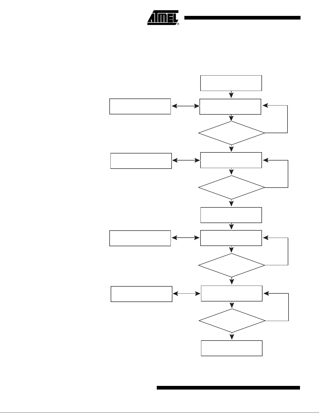
Appendix A
Controller Initialization
AT77C105A [Preliminary]
Host Controller
Initialization
Controller
Initialized ?
Yes
SPI Initialization
(Phase = 0, Polarity = 1)
SPI
Initialized
?
No
No
Yes
RST = 1
Sensor Initialization
RST = 0
Pulse
> 10 us ?
Yes
No
5419A–BIOM–01/05
35
Page 36
Appendix B
Example for the MODECTRL Register
Sensor
Controller
Interrupts Masked
SSS/ = 0
Reception of the Command
Reading of MODECTRL
Sending of MODECTRL
Reception of the Command
Writing of MODECTRL
MODECTRL Reading
Requested
Sending 0b11000100
Transfer
Ended ?
Modification of MODECTRL to
Change Mode Bits
Transfer
Ended ?
Modification of MODECTRL to
Change Mode Bits
MODECTRL Writing Requested
Sending of 0b10000100
Yes
Yes
No
No
36
Reception of MODECTRL
AT77C105A [Preliminary]
Transfer
ended ?
Yes
Sending of the New
MODECTRL
Transfer
ended ?
Yes
SSS/ = 1
Interrupts enabled
No
No
5419A–BIOM–01/05
Page 37

Appendix C
Example of Navigation Registers
Sensor
AT77C105A [Preliminary]
Controller
Interrupts Masked
SSS/ = 0
Reception of the Command
Reading of NAVIGATION
Sending of NAVIG1
Sending of NAVIG2
NAVIGATION Reading
Requested
Sending 0b11000000
Transfer
Ended ?
Sending of Dummy Data
0b00000000
Reception of NAVIG1
Transfer
Ended ?
Sending of Dummy Data
0b00000000
Reception of NAVIG2
Transfer
Ended ?
Yes
Yes
No
No
No
5419A–BIOM–01/05
Sending of NAVIG3
Yes
Sending of Dummy Data
0b00000000
Reception of NAVIG3
Interrupts Enabled
Transfer
Ended ?
Yes
SSS/ = 1
No
37
Page 38

Appendix D
Example of an Interrupt Generated by a Movement Detection
Controller
Main Program
Sensor
Interrupt Generated
IRQ/ = 0
Reception of the Command
Sending of STATUS
Interrupts Cleared
Reception of the Command
Reading of NAVIGATION
Interrup ?
Interrupts Masked
SSS/ = 0
STATUS Reading Requested
Sending of 0b11000000
Transfer
Ended ?
Yes
Sending of Dummy Data
0b00000000
Reception of STATUS
Transfer
Ended ?
Yes
Interrupts Control
Detection of Movement
NAVIGATION Reading
Requested
Sending of 0b11100000
No
No
No
38
Sending of the 3
Navigation Registers
AT77C105A [Preliminary]
Transfer
Ended ?
Yes
Sending of Dummy Data
0b00000000
Reception of the 3 Navigations
3 Registers
Values Sent ?
Interrupts enabled
Yes
SSS/ = 1
No
No
5419A–BIOM–01/05
Page 39

Atmel Corporation Atmel Operations
2325 Orchard Parkway
San Jose, CA 95131, USA
Tel: 1(408) 441-0311
Fax: 1(408) 487-2600
Regional Headquarters
Europe
Atmel Sarl
Route des Arsenaux 41
Case Postale 80
CH-1705 Fribourg
Switzerland
Tel: (41) 26-426-5555
Fax: (41) 26-426-5500
Asia
Room 1219
Chinachem Golden Plaza
77 Mody Road Tsimshatsui
East Kowloon
Hong Kong
Tel: (852) 2721-9778
Fax: (852) 2722-1369
Japan
9F, Tonetsu Shinkawa Bldg.
1-24-8 Shinkawa
Chuo-ku, Tokyo 104-0033
Japan
Tel: (81) 3-3523-3551
Fax: (81) 3-3523-7581
Memory
2325 Orchard Parkway
San Jose, CA 95131, USA
Tel: 1(408) 441-0311
Fax: 1(408) 436-4314
Microcontrollers
2325 Orchard Parkway
San Jose, CA 95131, USA
Tel: 1(408) 441-0311
Fax: 1(408) 436-4314
La Chantrerie
BP 70602
44306 Nantes Cedex 3, France
Tel: (33) 2-40-18-18-18
Fax: (33) 2-40-18-19-60
ASIC/ASSP/Smart Cards
Zone Industrielle
13106 Rousset Cedex, France
Tel: (33) 4-42-53-60-00
Fax: (33) 4-42-53-60-01
1150 East Cheyenne Mtn. Blvd.
Colorado Springs, CO 80906, USA
Tel: 1(719) 576-3300
Fax: 1(719) 540-1759
Scottish Enterprise Technology Park
Maxwell Building
East Kilbride G75 0QR, Scotland
Tel: (44) 1355-803-000
Fax: (44) 1355-242-743
RF/Automotive
Theresienstrasse 2
Postfach 3535
74025 Heilbronn, Germany
Tel: (49) 71-31-67-0
Fax: (49) 71-31-67-2340
1150 East Cheyenne Mtn. Blvd.
Colorado Springs, CO 80906, USA
Tel: 1(719) 576-3300
Fax: 1(719) 540-1759
Biometrics/Imaging/Hi-Rel MPU/
High Speed Converters/RF Datacom
Avenue de Rochepleine
BP 123
38521 Saint-Egreve Cedex, France
Tel: (33) 4-76-58-30-00
Fax: (33) 4-76-58-34-80
Literature Requests
www.atmel.com/literature
Disclaimer: The information in this document is provided in connection with Atmel products. No license, express or implied, by estoppel or otherwise, to any
intellectual property right is granted by this document or in connection with the sale of Atmel products. EXCEPT AS SET FORTH IN ATMEL’S TERMS AND CONDI-
TIONS OF SALE LOCATED ON ATMEL’S WEB SITE, ATMEL ASSUMES NO LIABILITY WHATSOEVER AND DISCLAIMS ANY EXPRESS, IMPLIED OR STATUTORY
WARRANTY RELATING TO ITS PRODUCTS INCLUDING, BUT NOT LIMITED TO, THE IMPLIED WARRANTY OF MERCHANTABILITY, FITNESS FOR A PARTICULAR
PURPOSE, OR NON-INFRINGEMENT. IN NO EVENT SHALL ATMEL BE LIABLE FOR ANY DIRECT, INDIRECT, CONSEQUENTIAL, PUNITIVE, SPECIAL OR INCIDENTAL DAMAGES (INCLUDING, WITHOUT LIMITATION, DAMAGES FOR LOSS OF PROFITS, BUSINESS INTERRUPTION, OR LOSS OF INFORMATION) ARISING OUT
OF THE USE OR INABILITY TO USE THIS DOCUMENT, EVEN IF ATMEL HAS BEEN ADVISED OF THE POSSIBILITY OF SUCH DAMAGES. Atmel makes no
representations or warranties with respect to the accuracy or completeness of the contents of this document and reserves the right to make changes to specifications
and product descriptions at any time without notice. Atmel does not make any commitment to update the information contained herein. Atmel’s products are not
intended, authorized, or warranted for use as components in applications intended to support or sustain life.
© Atmel Corporation 2005. All rights reserved. Atmel®, logo and combinations thereof, and FingerChip® and others, are registered trade-
marks, and Everywhere You Are
be trademarks of others.
SM
and others are the trademarks of Atmel Corporation or its subsidiaries. Other terms and product names may
Printed on recycled paper.
5419A–BIOM–01/05
 Loading...