

Page 1
1. Features
• Sensitive Layer Over a 0.35 µm CMOS Array
• Image Zone: 0.4 x 14 mm = 0.02" x 0.55"
• Image Array: 8 x 280 = 2240 pixels
• Pixel Pitch: 50 µm x 50 µm = 500 dpi
• Pixel Clock: up to 2 MHz Enabling up to 1780 Frames per Second
• Die Size: 1.64 x 17.46 mm
• Operating Voltage: 3V to 3.6V
• Naturally Protected Against ESD: > 16 kV Air Discharge
• Power Consumption: 16 mW at 3.3V, 1 MHz, 25°C
• Operating Temperature Range: -40°C to +85°C
• Chip-on-Board (COB), Chip-on-Board (COB) with Connector
• Complies With the European Directive for Restriction of Hazardous Substances
(RoHS Directive)
2. Applications
• PDA (Access Control, Data Protection)
• Notebook, PC-add on (Access Control, e-business)
• PIN Code Replacement
• Automated Teller Machines, POS
• Building Access
• Electronic Keys (Cars, Home)
• Portable Fingerprint Imaging for Law Enforcement
• TV Access
Thermal
Fingerprint
Sensor with
0.4 mm x 14 mm
(0.02" x 0.55")
Sensing Area
and
Digital Output
(On-chip ADC)
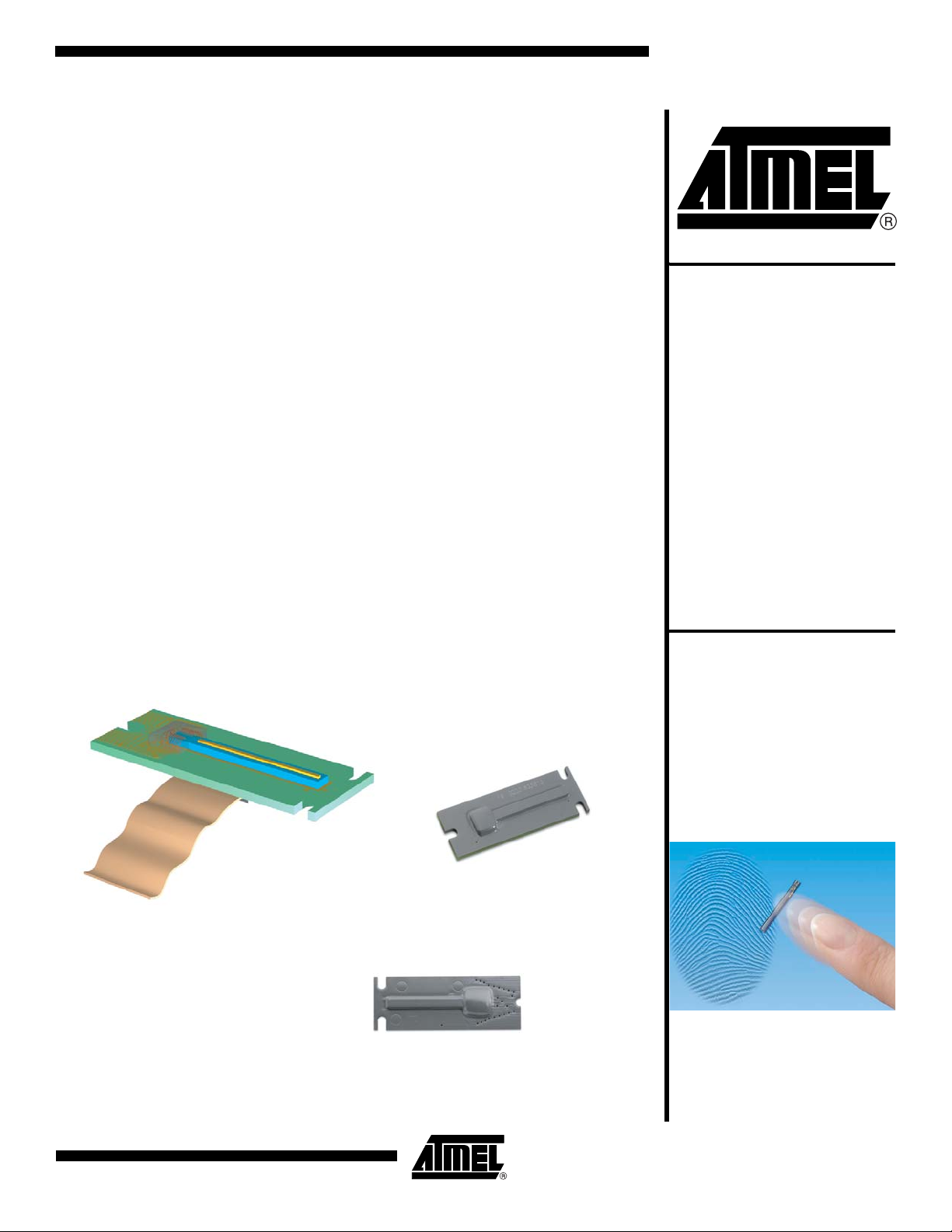
Figure 2-1. FingerChip® Packages
Chip-on-board Package
with Connector
Chip-on-board Package
Actual size
AT77C102B
FingerChip®
(COB)
Rev. 5364A–BIOM–09/05
Page 2
Table 2-1. Pin Description for Chip-on-Board Package: AT77C102B-CB01YV
Pin Number Name Type
1GNDGND
2 AVE Analog output
3 AVO Analog output
4TPPPower
5 TPE Digital input
6VCCPower
7GNDGND
8 RST Digital input
9 PCLK Digital input
10 OE Digital input
11 ACKN Digital output
12 De0 Digital output
13 Do0 Digital output
14 De1 Digital output
15 Do1 Digital output
16 De2 Digital output
17 Do2 Digital output
18 De3 Digital output
19 Do3 Digital output
20 FPL GND
21 GND GND
The die attach is connected to pins 1, 7 and 21, and must be grounded. The FPL pin must be
grounded.
GND
AVE
AVO
TPP
TPE
VCC
GND
RST
PCLK
OE
ACKN
De0
Do0
De1
Do1
De2
Do2
De3
Do3
FPL
GND
2
AT77C102B
1
2
3
4
5
6
7
8
9
10
11
12
13
14
15
16
17
18
19
20
21
5364A–BIOM–09/05
Page 3

AT77C102B
Table 2-2. Pin Description for COB with Connector Package: AT77C102B-CB02YV
Pin Number Name Type
1FPLGND
2 Not connected
3 Not connected
4 DE3 Digital output
5 DO3 Digital output
6 DE2 Digital output
7 DO2 Digital output
8 DE1 Digital output
9 DO1 Digital output
10 DE0 Digital output
11 DO0 Digital output
12 AVE Analog output
13 AVO Analog output
14 TPP Power
15 TPE Digital input
16 VCC Power
17 GND GND
(1)
18 RST Digital input
19 PCLK Digital input
20 OE Digital input
21 ACKN Digital output
Note: 1. Ref. Connector: FH18-21S-0.3SHW (HIROSE).
5364A–BIOM–09/05
3
Page 4
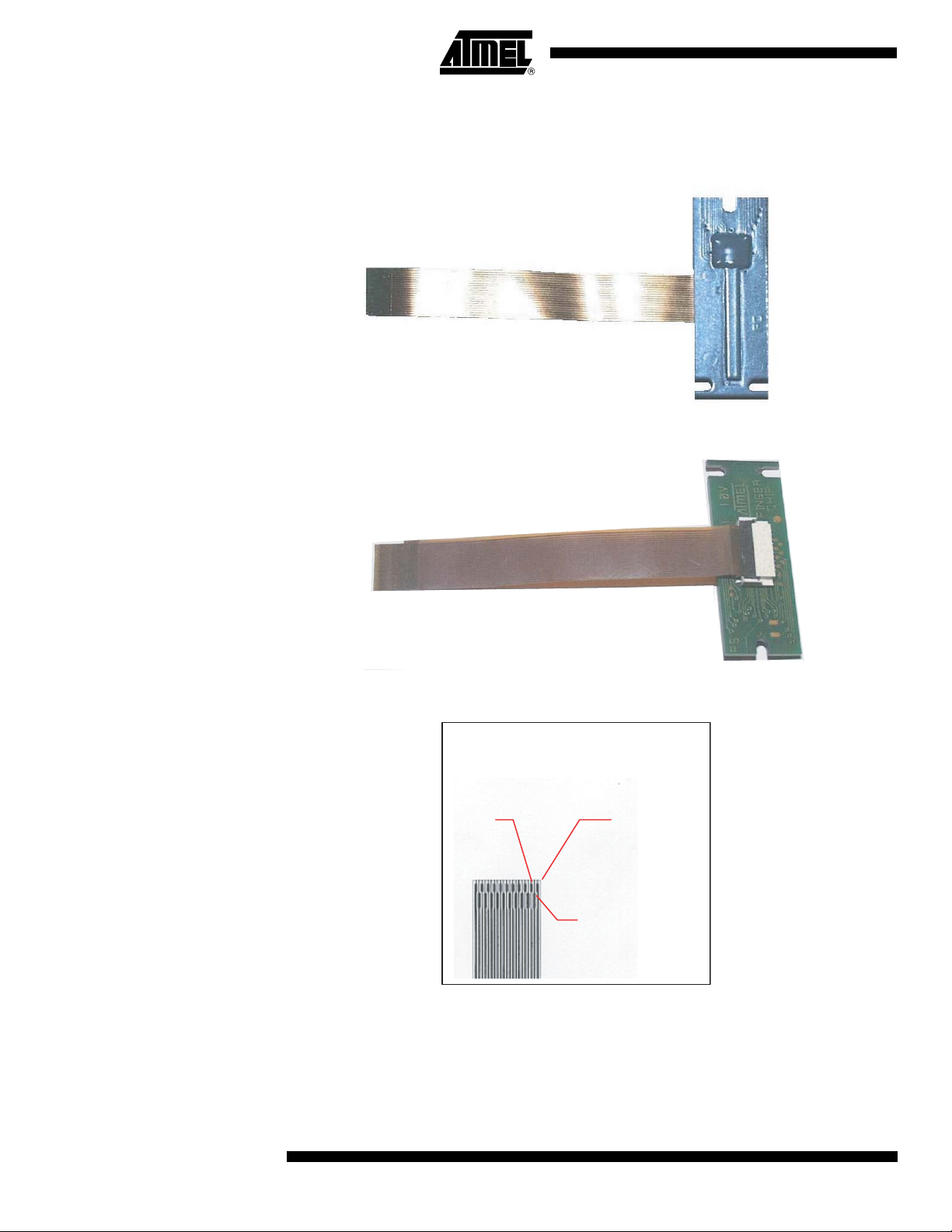
Figure 2-2. COB with Flex
(1)
Flex with metallizations up
Flex with metallizations down
Figure 2-3. Flex Output Side
1
3
Note: 1. Flex is not provided by Atmel.
(FingerChip Connector Side)
Flex Output
Metallizations Up
2
4
AT77C102B
5364A–BIOM–09/05
Page 5
3. Description
AT77C102B
The AT77C102B is part of the Atmel FingerChip monolithic fingerprint sensor family for which no
optics, no prism and no light source are required.
The AT77C102B is a single-chip, high-performance, low-cost sensor based on temperature
physical effects for fingerprint sensing.
The AT77C102B has a linear shape, which captures a fingerprint image by sweeping the finger
across the sensing area. After capturing several images, Atmel proprietary software can reconstruct a full 8-bit fingerprint image.
The AT77C102B has a small surface combined with CMOS technology, and a Chip-on-Board
package assembly. These facts contribute to a low-cost device.
The device delivers a programmable number of images per second, while an integrated analogto-digital converter delivers a digital signal adapted to interfaces such as an EPP parallel port, a
USB microcontroller or directly to microprocessors. No frame grabber or glue interface is therefore necessary to send the frames. These facts make AT77C102B an easy device to include in
any system for identification or verification applications.
Table 3-1. Absolute Maximum Ratings
()
Parameter Symbol Comments Value
Positive supply voltage V
Temperature stabilization
power
CC
TPP GND to 4.6
Front plane FPL GND to V
Digital input voltage RST PCLK GND to V
Storage temperature T
Lead temperature
(soldering, 10 seconds)
T
stg
leads
Do not solder Forbidden
GND to 4.6 Note: Stresses beyond those listed
under “Absolute Maximum Ratings”
may cause permanent damage to the
device. These are stress ratings only
CC
CC
-50 to +95
+0.5
+0.5
and functional operation of the device at
these or any other conditions beyond
those indicated in the operational
sections of this specification is not
implied. Exposure to absolute
maximum rating conditions for extended
periods may affect device reliability.
Table 3-2. Recommended Conditions Of Use
Parameter Symbol Comments Min Typ Max Unit
Positive supply voltage V
CC
Front plane FPL Must be grounded GND V
Digital input voltage CMOS levels V
Digital output voltage CMOS levels V
Digital load C
Analog load
Operating temperature range T
C
R
amb
L
A
A
Not connected
V grade -40°C to +85°C°C
Maximum current on TPP ITPP 0 100 mA
3V 3.3V 3.6V V
50 pF
pF
kΩ
5364A–BIOM–09/05
5
Page 6
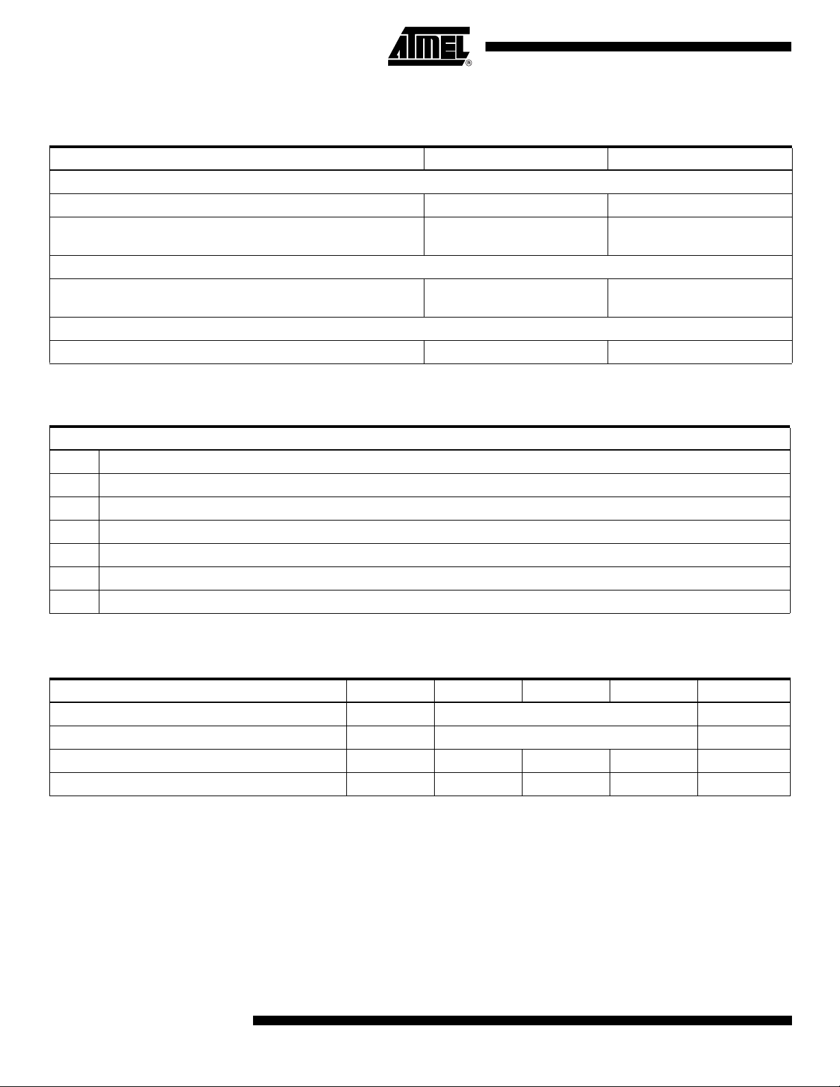
Table 3-3. Resistance
Parameter Min Value Standard Method
ESD
On pins. HBM (Human Body Model) CMOS I/O 2 kV MIL-STD-883 - method 3015.7
On die surface (Zapgun)
Air discharge
Mechanical Abrasion
Number of cycles without lubricant multiply by an estimated factor
of 20 for correlation with a real finger
Chemical Resistance
Cleaning agent, acid, grease, alcohol, diluted acetone 4 hours Internal method
±16 kV
200 000 MIL E 12397B
NF EN 6100-4-2
Table 3-4. Specifications
Explanation Of Test Levels
I 100% production tested at +25°C
II 100% production tested at +25°C, and sample tested at specified temperatures (AC testing done on sample)
III Sample tested only
IV Parameter is guaranteed by design and/or characterization testing
V Parameter is a typical value only
VI 100% production tested at temperature extremes
D 100% probe tested on wafer at T
= +25°C
amb
Table 3-5. Physical Parameter
Parameter Test Level Min Typ Max Unit
Resolution IV 50 µm
Size IV 8 x 280 Pixel
Yield: number of bad pixels I 5 Bad pixels
Equivalent resistance on TPP pin I 20 30 47 Ω
6
AT77C102B
5364A–BIOM–09/05
Page 7

AT77C102B
.
Table 3-6. 3.3V Power supply
The following characteristics are applicable to the operating temperature -40°C ≤ Ta ≤ +85°C
Typical conditions are: V
C
120 pF on digital outputs, analog outputs disconnected unless otherwise specified
load
Parameter Symbol Test Level Min Typ Max Unit
Power Requirements
= +3.3 V; T
CC
= 25°C; F
amb
= 1 MHz; Duty cycle = 50%
PCLK
Positive supply voltage V
Active current on V
Current on V
CC
Power dissipation on V
= 0
C
load
Current on V
CC
pin, 1 MHz
CC
pin, in static mode C
CC
load
= 0 pF
in NAP mode I
CCNAP
CC
I
CC
P
CC
I
IV
I
IV
I10µA
3.0 3.3 3.6 V
5
4
16
13
Analog Output
Voltage range V
AVx
IV 0 2.9 V
Digital Inputs
Logic compatibility CMOS
Logic “0” voltage V
Logic “1” voltage V
Logic “0” current I
Logic “1”current I
TPE logic “0” voltage I
TPE logic “1” voltage I
IL
IH
IL
IH
IL
IH
TPE 1 -10 0 µA
TPE 1 0 300 µA
I0 0.8V
I2.3 VCCV
I-10 0µA
I 0 10 µA
Digital Outputs
Logic compatibility CMOS
Logic “0” voltage
Logic “1” voltage
(1)
(1)
V
OL
V
OH
I0.6V
I2.4 V
25
18
7
5
mA
mA
mW
mW
Note: 1. With IOL = 1 mA and IOH = -1 mA
5364A–BIOM–09/05
7
Page 8

Table 3-7. Switching Performances
.
The following characteristics are applicable to the operating temperature -40°C ≤ Ta ≤ +85°C
Typical conditions are: nominal voltage; T
C
120 pF on digital and analog outputs unless otherwise specified
load
Parameter Symbol Test Level Min Typ Max Unit
= 25°C; F
amb
= 1 MHz; Duty cycle = 50%
PCLK
Clock frequency f
Clock pulse width (high) t
Clock pulse width (low) t
Clock setup time (high)/reset falling edge t
No data change t
Reset pulse width high t
PCLK
HCLK
LCLK
Setup
NOOE
HRST
I0.512MHz
I 250 ns
I 250 ns
I0ns
IV 100 ns
IV 50 ns
Table 3-8. 3.3V ±10% Power Supply
Parameter Symbol Test Level Min Typ Max Unit
Output delay from PCLK to ACKN rising edge t
Output delay from PCLK to ACKN falling edge t
Output delay from PCLK to data output Dxi t
Output delay from PCLK to analog output AVx t
Output delay from OE to data high-Z t
Output delay from OE to data output t
PLHACKN
PHLACKN
PDATA
PAV I D EO
DATA Z
ZDATA
I 145 ns
I 145 ns
I 120 ns
I 250 ns
IV 34 ns
IV 47 ns
Figure 3-1. Reset
8
Reset RST
Clock PCLK
AT77C102B
t
HRST
t
SETUP
5364A–BIOM–09/05
Page 9

Figure 3-2. Read One Byte/Two Pixels
f
PCLK
AT77C102B
Clock
PCLK
Acknowledge
ACKN
Data output
Do0-3, De0-3
Video analog output
AVO, AVE
Figure 3-3. Output Enable
t
HCLK
t
PLHACKN
Data #N
Data #N-1
t
PAVIDEO
t
LCLK
t
PHLACKN
Data #N
Data #N+1
t
PDATA
Data #N+1
Data #N+2
Output enable
OE
Data output
Do0-3, De0 -3
t
ZDATA
Hi-Z
Data output
t
DATAZ
Hi-Z
5364A–BIOM–09/05
9
Page 10

Figure 3-4. No Data Change
t
PCLK
OE
NOOE
Note: OE must not change during TNOOE after the PCLK falls. This is to ensure that the output drivers of the data are not driving cur-
rent, so as to reduce the noise level on the power supply.
Figure 3-5. AT77C102B Block Diagram
PCLK
RST
Column selection
1
8 lines of 280 columns of pixels
8
Chip temperature
stabilizati
TPP
3.1 Functional Description
The circuit is divided into two main sections: sensor and data conversion. One particular column
among 280 plus one is selected in the sensor array (1), then each pixel of the selected column
sends its electrical information to the amplifiers (2) [one per line], then two lines at a time are
selected (odd and even) so that two particular pixels send their information to the input of two 4bit analog-to-digital converters (3), so two pixels can be read for each clock pulse (4).
on
Clock
Reset
1 dummy colum
n
2240
temperature
8
Chip
sensor
Line sel
Amp
Ev
en
Odd
Analog
output
4-bit
ADC
4-bit
ADC
ACKN
4
8
Latches
4
Output
enable
OEAVE AVOTPE
De0-3
Do0-3
10
AT77C102B
5364A–BIOM–09/05
Page 11

Figure 3-6. Functional Description
AT77C102B
1 2 3 4
Column selection Line sel
8 lines of 280 columns of pixels
1 dummy colum
Amp
8
n
Chip
temperature
sensor
Ev
en
Odd
4-bit
ADC
4-bit
ADC
4
8
latches
4
3.2 Sensor
Each pixel is a sensor in itself. The sensor detects a temperature difference between the beginning of an acquisition and the reading of the information: this is the integration time. The
integration time begins with a reset of the pixel to a predefined initial state. Note that the integration time reset has nothing to do with the reset of the digital section.
Then, at a rate depending on the sensitivity of the pyroelectric layer, on the temperature variation between the reset and the end of the integration time, and for the duration of the integration
time, electrical charges are generated at the pixel level.
3.3 Analog-to-digital Converter/ Reconstructing an 8-bit Fingerprint Image
An analog-to-digital converter (ADC) is used to convert the analog signal coming from the pixel
into digital data that can be used by a processor.
De0-3
Do0-3
As the data rate for the parallel port and the USB is in the range of 1 MB per second, and at least
a rate of 500 frames per second is needed to reconstruct the image with a fair sweeping speed
of the finger, two 4-bit ADCs have been used to output two pixels at a time on one byte.
3.4 Start Sequence
A reset is not necessary between each frame acquisition.
The start sequence must consist in:
1. Setting the RST pin to high.
2. Setting the RST pin to low.
3. Sending 4 clock pulses (due to pipe-line).
4. Sending clock pulses to skip the first frame.
Note that after a reset it is recommended to skip the first 200 slices to stabilize the acquisition.
Figure 3-7. Start Sequence
Reset RS
Clock PCLK
T 4 + 1124 clock pulses to skip the first frame
1431 2 11124
5364A–BIOM–09/05
11
Page 12

3.5 Reading the Frames
A frame consists of 280 true columns plus one dummy column of eight pixels. As two pixels are
output at a time, a system must send 281 x 4 = 1124 clock pulses to read one frame.
Reset must be low when reading the frames.
3.6 Read One Byte/Output Enable
The clock is taken into account on its falling edge and data is output on its rising edge.
For each clock pulse, after the start sequence, a new byte is output on the Do0-3 and De0-3
pins. This byte contains two pixels: 4-bit on Do0-3 (odd pixels), 4-bit on De0-3 (even pixels).
To output the data, the output enable (OE) pin must be low. When OE is high, the Do0-3 and
De0-3 pins are in high-impedance state. This facilitates an easy connection to a microprocessor
bus without additional circuitry since the data output can be enabled using a chip select signal.
Note that the AT77C102B always sends data: there is no data exchange to switch to read/write
mode.
3.7 Power Supply Noise
IMPORTANT: When a falling edge is applied on OE (that is when the Output Enable becomes
active), then some current is drained from the power supply to drive the eight outputs, producing
some noise. It is important to avoid such noise just after the PCLK clock’s falling edge, when the
pixels’ information is evaluated: the timing diagram (Figure 3-2) and time T
val time when the power supply must be as quiet as possible.
define the inter-
NOOE
3.8 Video Output
3.9 Pixel Order
Figure 3-8. Pixel Order
Pixel #1 (1,1)
Pixel #8 (1,8)
An analog signal is also available on pins AVE and AVO. Note that video output is available one
clock pulse before the corresponding digital output (one clock pipe-line delay for the analog to
digital conversion).
After a reset, pixel 1 is located on the upper left corner, looking at the chip with bond pads to the
right. For each column of eight pixels, pixels 1, 3, 5 and 7 are output on odd data Do0-3 pins,
and pixels 2, 4, 6 and 8 are output on even data De0-3 pins. The Most Significant Bit (MSB) is bit
3, and the Least Significant Bit is bit 0.
Pixel #2233 (280,1)
ads
p
B ond
Pixel #2240 (280,8)
12
AT77C102B
5364A–BIOM–09/05
Page 13

3.10 Synchronization: The Dummy Column
A dummy column has been added to the sensor to act as a specific pattern to detect the first
pixel. Therefore, 280 true columns plus one dummy column are read for each frame.
The four bytes of the dummy column contain a fixed pattern on the first two bytes, and temperature information on the last two bytes.
Table 1. Dummy Column Description
Dummy Byte Odd Even
Dummy Byte 1 DB1: 111X 0000
Dummy Byte 2 DB2: 111X 0000
Dummy Byte 3 DB3: rrrr nnnn
Dummy Byte 4 DB4: tttt pppp
Note: x represents 0 or 1
The sequence 111X0000 111X0000 appears on every frame (exactly every 1124 clock pulses),
so it is an easy pattern to recognize for synchronization purposes.
3.11 Thermometer
The dummy bytes DB3 and DB4 contain some internal temperature information.
AT77C102B
The even nibble nnnn in DB3 can be used to measure an increase or decrease of the chip’s temperature, using the difference between two measures of the same physical device. The following
table gives values in Kelvin.
Table 1. Temperature Table
nnnn
Decimal
15 1111
14 1110
13 1101
12 1100
11 1011
10 1010
9 1001
8 1000
7 0111
6 0110
5 0101
4 0100
3 0011
2 0010
1 0001
0 0000
nnnn
Binary
Temperature differential with code 8
in Kelvin
> 11.2
8.4
7
5.6
4.2
2.8
1.4
0
-1.4
-2.8
-4.2
-5.6
-7
-8.4
-11.2
< -16.8
5364A–BIOM–09/05
13
Page 14

For code 0 and 15, the absolute value is a minimum (saturation).
When the image contrast becomes faint because of a low temperature difference between the
finger and the sensor, it is recommended to use the temperature stabilization circuitry to
increase the temperature by two codes (that is from 8 to 10), so as to obtain a sensor increase of
at least >1.4 Kelvin. This enables enough contrast to obtain a proper fingerprint reconstruction.
3.12 Integration Time and Clock Jitter
The AT77C102B is not very sensitive to clock jitters (clock variations). The most important
requirement is a regular integration time that ensures the frame reading rate is also as regular as
possible, so as to obtain consistent fingerprint slices.
If the integration time is not regular, the contrast can vary from one frame to another.
Note that it is possible to introduce some waiting time between each set of 1124 clock pulses,
but the overall time of one frame read must be regular. This waiting time is generally the time
needed by the processor to perform some calculation over the frame (to detect the finger, for
instance).
Figure 3-9. Read One Frame
Reset RST is lo
Clock PCLK
w
123456 112411231122112111201119
Column 1 Column 2 Column 280 Dummy Column 281
Pixels 1 & 2 3 & 4 5 & 6 7 & 8 1 & 2 3 & 4 7 & 8 DB1 DB2 DB3 DB
Figure 3-10. Regular Integration Time
Frame n
Clock PCLK
1124 pulses
3.13 Power Management
3.14 Nap Mode
Several strategies are possible to reduce power consumption when the device is not in use.
The simplest and most efficient is to cut the power supply using external means.
A nap mode is also implemented in the AT77C102B. To activate this nap mode, you must:
1. Set the reset RST pin to high. By doing this, all analog sections of the device are internally powered down.
2. Set the clock PCLK pin to high (or low), thus stopping the entire digital section.
3. Set the TPE pin to low to stop the temperature stabilization feature.
4. Set the Output Enable OE pin to high, so that the output is forced in HiZ.
REGULAR INTEGRATION TIME
Frame n+1
1124 pulses
Frame n+2
1124 pulses
Frame n+3
1124 pulse
4
s
14
AT77C102B
5364A–BIOM–09/05
Page 15

Figure 3-11. Nap Mode
AT77C102B
Nap mode
Reset RS
Clock PCLK
T
Nap
In nap mode, all internal transistors are in shut mode. Only leakage current is drained in the
power supply, generally less than the tested value.
3.15 Static Current Consumption
When the clock is stopped (set to 1) and the reset is low (set to 0), the device’s analog sections
drain some current, whereas, if the outputs are connected to a standard CMOS input, the digital
section does not consume any current (no current is drained in the I/O). In this case the typical
current value is 5 mA. This current does not depend on the voltage (it is almost the same from 3
to 3.6V).
3.16 Dynamic Current Consumption
When the clock is running, the digital sections, and particularly the outputs if they are heavily
loaded, consume current. In any case, the current should be less than the testing machine (120
pF load on each I/O), and a maximum of 50 pF is recommended.
The AT77C102B, running at about 1 MHz, consumes less than 7 mA on the V
3.17 Temperature Stabilization Power Consumption (TPP Pin)
When the TPE pin is set to 1, current is drained via the TPP pin. The current is limited by the
internal equivalent resistance given in Table 3-4 on page 6 and a possible external resistor.
CC
pin.
Most of the time, TPE is set to 0 and no current is drained in TPP. When the image contrast
becomes low because of a low temperature differential (less than 1 Kelvin), then it is recommended to set TPE to 1 for a short time so that the dissipated power in the chip elevates the
temperature, allowing contrast recovery. The necessary time to increase the chip’s temperature
by one Kelvin depends on the dissipated power, the thermal capacity of the silicon sensor and
the thermal resistance between the sensor and its surroundings. As a rule of thumb, dissipating
300 mW in the chip elevates the temperature by 1 Kelvin in one second. With the 30Ω typical
value, 300 mW is 3V applied on TPP. If the power supply is 3.6V, an external resistor must be
added in the application to limit the current under 100 mA.
5364A–BIOM–09/05
15
Page 16

4. Packaging: Mechanical Data
Figure 4-1. Product Reference: AT77C102B-CB01YV
TOP VIEW
SCALE 10/1
SIDE VIEW
SCALE 10/1
A
0.2 A
0.89 ±0.3
2.33 ±0.5
1.64
0.74 ±0.06
+0.07
At 0.4 heigh from B ref.
-0.01
0.32
Top View (all dimensions in mm)
1
4
min
0.2
26.6 ±0.3
0.2
max
max
5.20
Dam and Fill
5.90
max
1.5
max.
2.95 ±0.50
9 ±0.3
0.82 ±0.50
B
0.82 ±0.18
Figure 4-2. Product Reference: AT77C102B-CB01YV
Bottom View (All dimensions in mm)
+
_
0.08
+0.08
-0.12
(x3)
(x3)
1
+
_
0.08
0.5
6.30
+
_
0.15
1.15
+
_
2.15 0.15
+
_
0.1
+0.33
0.75
- 0.25
RO. 75
+0.15
1.5
- 0.23
23.85
+
_
0.08
3.5
+
_
0.15
1
+
_
0.08
1.5
+
_
0.08
2
+
_
0.15
2
+
_
0.1
16
AT77C102B
5364A–BIOM–09/05
Page 17

Figure 4-3. Product Reference: AT77C102B-CB02YV
All Dimensions in mm
9.85 ±0.3
5.9 max
5.2 max
14.32
AT77C102B
+0.04
-0.01
FLEX OUTPUT
2.9±0.5
1.5 MAX
0.2 min
4.1 Package Information
Scale 4/1
1.9±0.4
4.1 ±0.2
0.18
±
0.82
)
3
(x
+0.15
-0.23
1.5
A
1.64
+0.07
-0.01
8.9 ±0.5
8.8 ±0.2
1.25 ±0.5
26.6 ±0.3
FLEX OUTPUT
0.75
+0.33
-0.25
2.39 ±0.5
R0.75
0.08
+
-0.12
(x 3)
+
_
0.74 0.06
±0.5
4.1
(x 2)
6.3 ±0.1
1.78 ±0.5
A
4.1.1 Electrical Disturbances
When looking at the fingerchip device from the top with the glob top to the right, the right edge
must never be in contact with customer casing or any component to avoid electrical
disturbances.
Figure 4-4. Epoxy Overflow
Maximum epoxy overflow width: 0.55 mm on the die edge.
Maximum epoxy overflow thickness: 0.33 mm.
Note: Refer to Figure 4-1 on page 16.
5364A–BIOM–09/05
AA Section
Fingerchip
0.55
0.33
Epoxy Glue Overflow
17
Page 18

5. Ordering Information
5.1 Package Device
Atmel prefix
FingerChip family
Device type
Package
CB01: Chip On Board (COB)
CB02: COB with connector
AT77C 102B- —
CBXX
VY
Quality level:
— : standard
Temperature range
o
V: -40
C to +85o C
RoHS compliant
18
AT77C102B
5364A–BIOM–09/05
Page 19

Atmel Corporation Atmel Operations
2325 Orchard Parkway
San Jose, CA 95131, USA
Tel: 1(408) 441-0311
Fax: 1(408) 487-2600
Regional Headquarters
Europe
Atmel Sarl
Route des Arsenaux 41
Case Postale 80
CH-1705 Fribourg
Switzerland
Tel: (41) 26-426-5555
Fax: (41) 26-426-5500
Asia
Room 1219
Chinachem Golden Plaza
77 Mody Road Tsimshatsui
East Kowloon
Hong Kong
Tel: (852) 2721-9778
Fax: (852) 2722-1369
Japan
9F, Tonetsu Shinkawa Bldg.
1-24-8 Shinkawa
Chuo-ku, Tokyo 104-0033
Japan
Tel: (81) 3-3523-3551
Fax: (81) 3-3523-7581
Memory
2325 Orchard Parkway
San Jose, CA 95131, USA
Tel: 1(408) 441-0311
Fax: 1(408) 436-4314
Microcontrollers
2325 Orchard Parkway
San Jose, CA 95131, USA
Tel: 1(408) 441-0311
Fax: 1(408) 436-4314
La Chantrerie
BP 70602
44306 Nantes Cedex 3, France
Tel: (33) 2-40-18-18-18
Fax: (33) 2-40-18-19-60
ASIC/ASSP/Smart Cards
Zone Industrielle
13106 Rousset Cedex, France
Tel: (33) 4-42-53-60-00
Fax: (33) 4-42-53-60-01
1150 East Cheyenne Mtn. Blvd.
Colorado Springs, CO 80906, USA
Tel: 1(719) 576-3300
Fax: 1(719) 540-1759
Scottish Enterprise Technology Park
Maxwell Building
East Kilbride G75 0QR, Scotland
Tel: (44) 1355-803-000
Fax: (44) 1355-242-743
RF/Automotive
Theresienstrasse 2
Postfach 3535
74025 Heilbronn, Germany
Tel: (49) 71-31-67-0
Fax: (49) 71-31-67-2340
1150 East Cheyenne Mtn. Blvd.
Colorado Springs, CO 80906, USA
Tel: 1(719) 576-3300
Fax: 1(719) 540-1759
Biometrics/Imaging/Hi-Rel MPU/
High Speed Converters/RF Datacom
Avenue de Rochepleine
BP 123
38521 Saint-Egreve Cedex, France
Tel: (33) 4-76-58-30-00
Fax: (33) 4-76-58-34-80
Literature Requests
www.atmel.com/literature
DDisclaimer: The information in this document is provided in connection with Atmel products. No license, express or implied, by estoppel or otherwise, to any
intellectual property right is granted by this document or in connection with the sale of Atmel products. EXCEPT AS SET FORTH IN ATMEL’S TERMS AND CONDI-
TIONS OF SALE LOCATED ON ATMEL’S WEB SITE, ATMEL ASSUMES NO LIABILITY WHATSOEVER AND DISCLAIMS ANY EXPRESS, IMPLIED OR STATUTORY
WARRANTY RELATING TO ITS PRODUCTS INCLUDING, BUT NOT LIMITED TO, THE IMPLIED WARRANTY OF MERCHANTABILITY, FITNESS FOR A PARTICULAR
PURPOSE, OR NON-INFRINGEMENT. IN NO EVENT SHALL ATMEL BE LIABLE FOR ANY DIRECT, INDIRECT, CONSEQUENTIAL, PUNITIVE, SPECIAL OR INCIDENTAL DAMAGES (INCLUDING, WITHOUT LIMITATION, DAMAGES FOR LOSS OF PROFITS, BUSINESS INTERRUPTION, OR LOSS OF INFORMATION) ARISING OUT
OF THE USE OR INABILITY TO USE THIS DOCUMENT, EVEN IF ATMEL HAS BEEN ADVISED OF THE POSSIBILITY OF SUCH DAMAGES. Atmel makes no
representations or warranties with respect to the accuracy or completeness of the contents of this document and reserves the right to make changes to specifications
and product descriptions at any time without notice. Atmel does not make any commitment to update the information contained herein. Unless specifically provided
otherwise, Atmel products are not suitable for, and shall not be used in, automotive applications. Atmel’s products are not intended, authorized, or warranted for use
as components in applications intended to support or sustain life.
© Atmel Corporation 2005. All rights reserved. Atmel®, logo and combinations thereof, Everywhere You Are®, FingerChp® and others, are
registered trademarks or trademarks of Atmel Corporation or its subsidiaries. Other terms and product names may be trademarks of others.
Printed on recycled paper.
5364A–BIOM–09/05
 Loading...