

Page 1

Features
• ARM7TDMI
• Two 16-bit Fixed-point OakDSPCore
• 256 x 32-bit Boot ROM
• 88K Bytes of Integrated Fast RAM for Each DSP
• Flexible External Bus Interface with Programmable Chip Selects
• Dual Codec Interface
• Multi-level Priority, Individually Maskable, Vectored Interrupt Controller
• Three 16-bit Timer/Counters
• Additional Watchdog Timer
• Two USARTs with FIFO and Modem Control Lines
• Industry-standard Serial Peripheral Interface
• Up to 23 General-purpose I/O Pins
• On-chip DRAM Controller
• JTAG Debug Interface
• Software Development Tools Available for ARM7TDMI and OakDSPCore
• Supported by a Wide Range of Ready-to-use Application Software, including
Multitasking Operating System, Networking, Modems and Voice-processing Functions
• Available in a 160-lead PQFP Package
• 3.3V Power Supply
™
ARM® Thumb® Processor Core
®
Cores
Description
The Atmel AT75C310 Smart Internet Appliance Processor (SIAP™) is a high-performance processor designed for internet appliance applications such as Internet Telephony (Voice over Internet Protocol – VoIP). The AT75C310 is built around an
ARM7TDMI microcontroller core running at 20 MIPS with two DSP co-processors running at 40 MIPS each. All three processors deliver unmatched performance for low
power consumption.
In a typical standalone VoIP phone, one DSP handles the voice-processing functions
(voice compression, acoustic echo cancellation, etc.) while the other deals with the
telephony functions such as dialing, line echo cancellation, caller ID detection, highspeed modem, etc. In such an application, the power of the ARM7TDMI allows it to
run the VoIP protocol stack as well as all the system control tasks.
Atmel provides the AT75C310 with three levels of software modules:
• A special port of the Linux kernel as the proposed operating system
• A comprehensive set of tunable DSP algorithms for modems and voice processing,
tailored to be run by the DSP subsystems
• A broad range of application-level software modules such as H323 telephony or
POP-3/SMTP e-mail services
Smart Internet
Appliance
Processor
(SIAP™)
AT75C310 –
CPU
Peripherals
Rev. 1369A–01/01
1
Page 2

AT75C310 Pin Configuration
Table 1. AT75C310 Pinout in 160-lead PQFP Package
Pin Signal Name Pin Signal Name Pin Signal Name Pin Signal Name
VDD
1
D11
2
NCE3
3
VSS
4
NDOE
5
D12
6
D13
7
NWE0
8
D14
9
VSS
10
VDD
11
NWE1
12
D15
13
NDWE
14
VDD
15
VDD
16
VSS
17
VSS
18
VDD
19
MOSI
20
MISO
21
SPCK
22
NPCSS
23
RXDA
24
TXDA
25
VSS
26
VDD
27
NRTSA
28
NCTSA
29
NDTRA
30
NDSRA/BOOTN
31
VSS
32
VDD
33
NDCDA
34
TXDB
35
RXDB
36
VDD
37
PB7/NCE1
38
VSS
39
VSS
40
VSS
41
PB6/NWDOVF
42
PB5/NRIA
43
PB4
44
VSS
45
VDD
46
PB3
47
RESET
48
VDD
49
IRQ0
50
PB2/TIOB1
51
PB9
52
PB1/TIOA1
53
PB8/NCE2
54
PB0/TCLK1
55
VDD
56
XREF80
57
VSS
58
XTALIN
59
XTALOUT
60
VSS
61
XREF96
62
VDD
63
TST
64
NTRST
65
TCK
66
TMS
67
TDI
68
TDO
69
VSS
70
PA0/OakAIN0
71
PA1/OakAIN1
72
PA2/OakAOUT0
73
PA3/OakAOUT1
74
VSS
75
VDD
76
PA4/OakBIN0
77
PA5/OakBIN1
78
PA6/OakBOUT0
79
PA7/OakBOUT1
80
81
82
83
84
85
86
87
88
89
90
91
92
93
94
95
96
97
98
99
100
101
102
103
104
105
106
107
108
109
110
111
112
113
114
115
116
117
118
119
120
VDD
PA8/TCLK0
PA 9 /T I O A 0
VSS
PA10/TIOB0
PA11/SCLKA
VSS
PA12/NPCS1
VDD
VSS
VDD
NREQ
FIQ
NGNT
VSS
VDD
SCLKA
FSA
STXA
SRXA
A0
A1
A2
A3
VDD
A4
A5
A6
A7
VDD
VSS
A8
A9
A10
A11
A12
A13
A14
A15
VSS
121
122
123
124
125
126
127
128
129
130
131
132
133
134
135
136
137
138
139
140
141
142
143
144
145
146
147
148
149
150
151
152
153
154
155
156
157
158
159
160
VSS
A16
A17
VDD
VSS
A18
A19
A20
A21
VDD
VSS
D0
NCAS0
D1
D2
NCAS1
D3
VSS
NRAS0
D4
NRAS1
VSS
VDD
D5
SRXB
STXB
D6
FSB
VDD
VSS
D7
SCLKB
D8
NSOE
VDD
VSS
NCE0
D9
D10
VDD
2
AT75C310
Page 3

AT75C310 Pin Description
Table 2. AT75C310 Pin Description
Block Pin Name Type Function
A[21:0] O Address Bus
AT75C310
Common Bus
Dynamic Memory
Controller
Static Memory
Controller
I/O Port A PA[12:0] I/O General Purpose I/O Lines. Multiplexed with peripheral I/Os
I/O Port B PB[9:0] I/O General Purpose I/O Lines. Multiplexed with peripheral I/Os
DSP Subsystem A
DSP Subsystem B
Timer/Counter 0
D[15:0] I/O Data Bus
NREQ I Bus Request
NGNT O Bus Grant
NRAS[1:0] O Row Address Strobe
NCAS[1:0] O Column Address Strobe
NDWE O DRAM Write Enable
NDOE O DRAM Output Enable
NCE[3:0] O Chip Selects
NWE[1:0] O Byte Select/Write Enable
NSOE O SRAM Output Enable
OakAIN[1:0] I OakDSPCore A User Inputs
OakAOUT[1:0] O OakDSPCore A User Outputs
OakBIN[1:0] I OakDSPCore B User Inputs
OakBOUT[1:0] O OakDSPCore B User Outputs
TCLK0 I Timer 0 External Clock
TIOA0 I/O Timer 0 Signal A
TIOB0 I/O Timer 0 Signal B
TCLK1 I Timer 1 External Clock
Timer/Counter 1
Watchdog NWDOVF O Watchdog Overflow
Serial Peripheral
Interface
TIOA1 I/O Timer 1 Signal A
TIOB1 I/O Timer 1 Signal B
MISO I/O Master In/Slave Out
MOSI I/O Master Out/Slave In
SPCK I/O Serial Clock
NPCSS I/O Chip Select/Slave Select
NPSC1 O Optional SPI Chip Select 1
3
Page 4

Table 2. AT75C310 Pin Description (Continued)
Block Pin Name Type Function
RXDA I Receive Data
TXDA O Transmit Data
NRTSA O Ready to Send
NCTSA I Clear To Send
USART A
NDTRA O Data Terminal Ready
NDSRA/BOOTN I Data Set Ready
NDCDA I Data Carrier Detect
NRIA I Ring Indicator
SCLKA I/O Serial Clock
USART B
JTAG Interface
Codec Interface A
Codec Interface B
RXDB I Receive Data
TXDB O Transmit Data
NTRST I JTAG Test Reset
TCK I JTAG Test Clock
TMS I JTAG Test Mode Select
TDI I JTAG Test Data Input
TDO O JTAG Test Data Output
SCLKA I/O Codec Serial Clock
FSA I/O Frame Sync Pulse
STXA O Transmit Data to Codec
SRXA I Receive Data from Codec
SCLKB I/O Codec Serial Clock
FSB I/O Frame Sync Pulse
STXB O Transmit Data to Codec
SRXB I Receive Data from Codec
RESET I Master Reset
FIQ/LOWP I Fast Interrupt/Low Power
IRQ0 I External Interrupt request
Miscellaneous
4
XREF96 I External 96 MHz PLL Reference
XREF80 I External 80 MHZ PLL Reference
XTALIN I External Crystal Input
XTALOUT O External Crystal Output
TST I Test Mode
AT75C310
Page 5
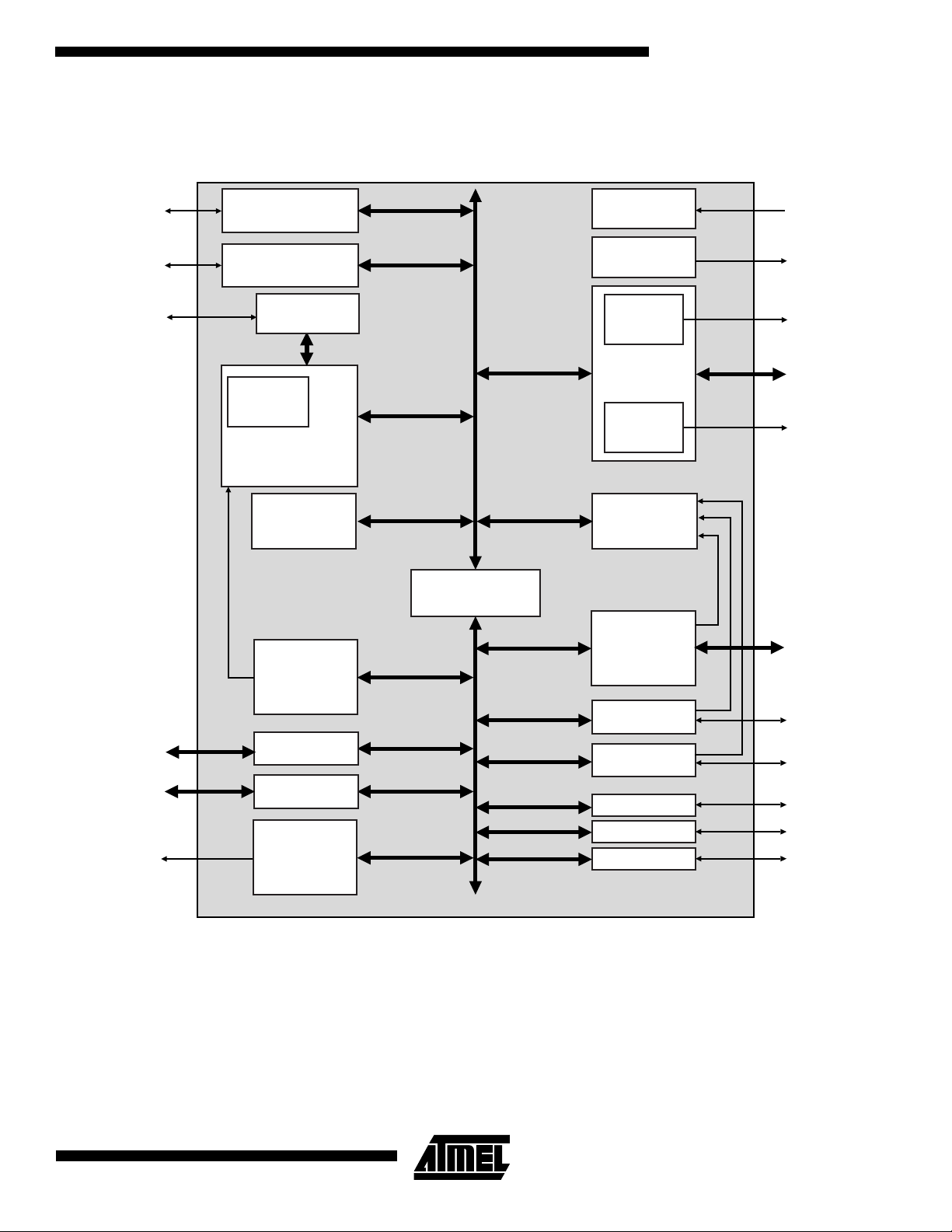
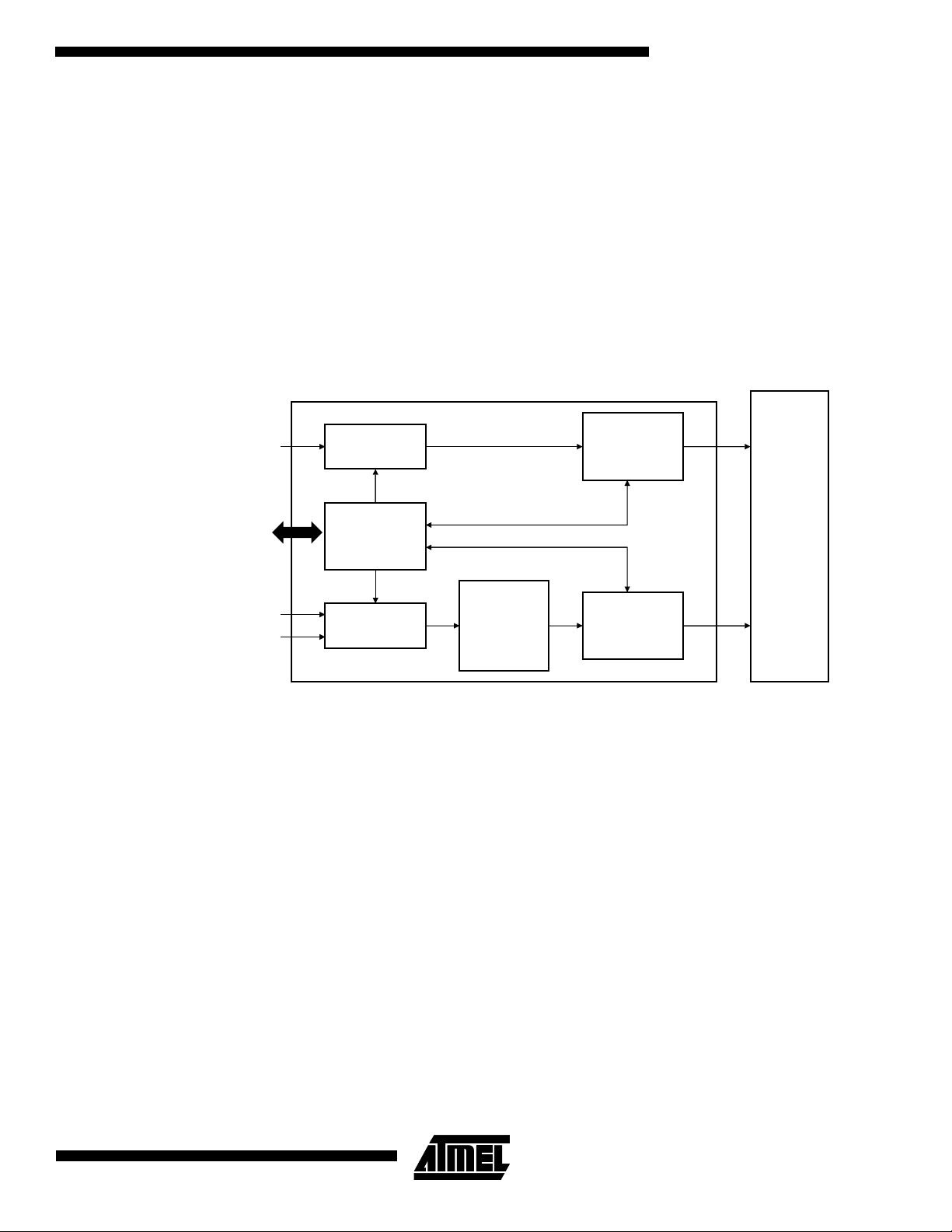
Block Diagram
Figure 1. AT75C310 Block Diagram
AT75C310
OakDSPCore 0
DSP Subsystem
OakDSPCore 1
DSP Subsystem
JTAG
Embedded
ICE
ARM7TDMI Core
Boot ROM
IRQ
Controller
AMBA
TM
ASB
Bridge
Reset
Clocks
DRAM
Controller
External Bus
Interface
SRAM
Controller
Peripheral Data
Controller
SPI
PIO 0
PIO 1
Watchdog
Timer
USART 0
USART 1
Timer/Counter 0
Timer/Counter 1
Timer/Counter 2
APB
5
Page 6

Architectural Overview
The AT75C310 architecture consists of two main buses,
the Advanced System Bus (ASB) and the Advanced
Peripheral Bus (APB).
The ASB is designed for maximum performance. It interfaces the processor with the on-chip DSP subsystems and
the external memories and devices by means of the External Bus Interface (EBI).
The APB is designed for accesses to on-chip peripherals
and is optimized for low power consumption. The AMBA
Bridge provides an interface between the ASB and the
APB.
An on-chip Peripheral Data Controller (PDC) transfers data
between the on-chip USARTs and the memories without
processor intervention. Most importantly, the PDC removes
the processor interrupt handling overhead and significantly
reduces the number of clock cycles required for a data
transfer. It can transfer up to 64K contiguous bytes without
reprogramming the starting address. As a result, microcontroller performance is increased and power consumption
reduced.
The AT75C310 peripherals are designed to be programmed with a minimum number of instructions. Each
peripheral has a 16 KB address space allocated in the
upper part of the address space. The peripheral register set
is composed of control, mode, data, status and interrupt
registers.
To maximize the efficiency of bit manipulation, frequentlywritten registers are mapped into three memory locations.
The first address is used to set the individual register bits,
the second resets the bits and the third address reads the
value stored in the register. A bit can be set or reset by writing a one to the corresponding position at the appropriate
address. Writing a zero has no effect. Individual bits can
™
thus be modified without having to use costly read-modifywrite and complex bit-manipulation instructions, and without having to store-disable-restore the interrupt state.
All external signals of the on-chip peripherals are controlled
by the parallel I/O controllers. The PIO controllers can be
programmed to insert an input filter on each pin or to generate an interrupt on a signal change. After reset, the user
must carefully program the PIO controllers in order to
define which peripheral signals are connected with off-chip
logic.
The ARM7TDMI processor operates in little-endian mode
in the AT75C310. The processor’s internal architecture and
the ARM and Thumb instruction sets are described in theAtmel ARM7TDMI datasheet, literature number 0673. The
memory map and the on-chip peripherals are described in
this datasheet. The DSP subsystems are described in the
datasheet entitled “AT75C310 DSP Subsystem”, literature
number 1368. Electrical characteristics are documented in
a separate datasheet entitled “AT75C310 Electrical and
Mechanical Characteristics”, literature number 1370.
PDC: Peripheral Data Controller
The AT75C310 has a four-channel PDC dedicated to the
two on-chip USARTs. One PDC channel is connected to
the receiving channel and one to the transmitting channel
of each USART.
The user interface of a PDC channel is integrated in the
memory space of each USART channel. It contains a 32-bit
address pointer register and a 16-bit count register. When
the programmed number of bytes is transferred, an end of
transfer interrupt is generated by the corresponding
USART. For more details on PDC operation and programming, see the section “USART: Universal Synchronous/Asynchronous Receiver/Transmitter” on page 53.
6
AT75C310
Page 7

Memory Map
The memory map is divided into memory regions of 64
megabytes. The top seven memory regions are reserved
and subdivided for internal memory blocks or peripherals
within the AT75C310. The AT75C310 can define up to six
other active external memory regions by means of the
static memory controller and DRAM memory controller.
The memory map assumes default values on reset. External memory regions can be reprogrammed to other base
addresses. For details, see the sections “SMC: Static
Memory Controller” on page 15 and “DMC: Dynamic Memory Controller” on page 24. It should be noted that the internal memory regions have fixed locations that cannot be
reprogrammed.
Table 3. Memory Map
Default Base Address Region Type Normal Mode
There are no hardware locks to prevent incorrect programming of the regions. Programming two or more regions to
have the same base address results in undefined behavior.
The ARM reset vector with address 0x00000000 is mapped
to internal ROM or external memory depending on the signal pin NDSRA/BOOTN. After booting, the ROM region can
be disabled and some external memory such as DRAM or
Flash can be mapped to the bottom of the memory map by
programming SMC_CS0 or DMC_MR0.
AT75C310
0xFF000000
0xFE000000
0xFD000000
0xFC000000
0xFB000000
0xFA000000
0xF9000000
0x50000000
0x40000000
0x30000000
0x20000000
0x10000000
0x00000000
Internal Peripherals
Internal OAK B (24K x 16 Program SRAM)
Internal OAK A (24K x 16 Program SRAM)
Internal Reserved
Internal Dual-port Mailbox for Oak B (2K x 16)
Internal Dual-port Mailbox for Oak A (2K x 16)
Internal Boot ROM (1K x 16)
External DMC_MR1
External DMC_MR0
External SMC_CS3
External SMC_CS2
External SMC_CS1
External/Internal SMC_CS0
Boot Mode
0x000003FF
Boot ROM
0x00000000
7
Page 8

Peripheral Memory Map
The register maps for each peripheral are described in the corresponding sections of this datasheet. The peripheral memory map has 16KB reserved for each peripheral.
Table 4. Peripheral Memory Map
Base Address Peripheral Description
0xFF000000 MODE Mode Controller
0xFF004000 SMC Static Memory Controller
0xFF008000 DMC DRAM Memory Controller
0xFF00C000 PIO A Programmable I/O
0xFF010000 PIO B Keypad PIO
0xFF014000 TC Timer/Counter Channels
0xFF018000 USART A USART
0xFF01C000 USART B USART
0xFF020000 SPI Serial Peripheral Interface
0xFF024000 Reserved
0xFF028000 WDT Watchdog Timer
0xFF030000 AIC Advanced Interrupt Controller
8
AT75C310
Page 9

Initialization
Reset initializes the user interface registers to their default
states as defined in the peripheral sections of this
datasheet and forces the ARM7TDMI to perform the next
instruction fetch from address zero. Except for the program
counter, the ARM core registers do not have defined reset
states. When reset is active, the inputs of the AT75C310
must be held at valid logic levels.
There are three ways in which the AT75C310 can enter
reset:
1. Hardware reset. Caused by asserting the RESET
pin, e.g., at power-up.
2. Watchdog timer reset. The watchdog timer can be
programmed so that if it is timed out, a pulse is generated that forces a chip reset.
3. Software reset. There are two software resets which
are asserted by writing to bits [11:10] of the
AT75C310 mode register. SIAP_MD[11] forces a
software reset with RM set low and SIAP_MD[10]
forces a reset with RM set high.
AT75C310
Reset Pin
The reset pin should be asserted for a minimum of 10 clock
cycles. However, if external DRAM is fitted, reset should be
applied for the time interval specified by the DRAM
datasheet, typically 200 µs. The OakDSPCores are only
released from reset by ARM program control.
When reset is released, the pin NDSRA/BOOTN is sampled to determine if the ARM should boot from internal
ROM or from external memory connected to NCS0. The
details of this boot operation are described in the section
“Boot Mode” on page 11.
Processor Synchronization
The ARM and the OakDSPCore processors have their own
PLLs and at power-on each processor has its own indeterminate lock period. To guarantee proper synchronization of
inter-processor communication through the mailboxes, a
specific reset sequence should be followed.
Once the ARM core is out of reset, it should set and clear
the reset line of each OakDSPCore three times. This guarantees message synchronization between the ARM and
the OakDSPCores.
9
Page 10
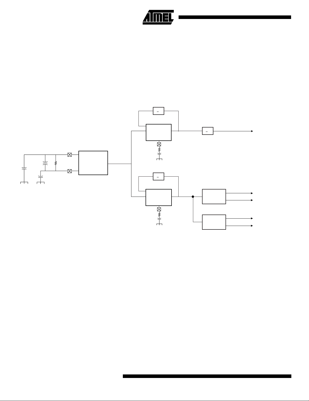
Clocking
The AT75C310 uses an external 16 MHz crystal (XCLK)
and two on-chip PLLs to generate the internal clocks. One
PLL generates a 96 MHz clock that is divided down to produce the ARM clocks and the other produces an 80 MHz
clock used to generate the Oak and Codec interface
clocks.
The ARM core runs at 24 MHz whereas the DSP subsystems run at 40 MHz.
Figure 2. AT75C310 Clock Circuitry Diagram
Note that there is a common synchronous mode where the
ARM and OAK systems both run from the Oak PLL. This
results in the ARM running at 20 MHz and the Oak at
40 MHz.
A block diagram of the clock circuitry can be seen below in
Figure 2.
.
.
6
10 pF
10 pF
16 MHz
XTAL
XTALIN
1 MΩ
XTALOUT
Oscillator
16 MHz
100 Ω
10 nF
100 Ω
10 nF
PLL
.
.
PLL
XREF 96
5
XREF 80
96 MHz
80 MHz
.
.
4
Phase
Generator
Phase
Generator
24 MHz
40 MHz
40 MHz
40 MHz
40 MHz
ARM Clock
Core
DSP Subsystem A
Clocks
DSP Subsystem B
Clocks
10
AT75C310
Page 11

Boot Mode
When the reset pin is deasserted, i.e., when the AT75C310
exits from reset state, the NDSRA/BOOTN pin is sampled.
If NDSRA/BOOTN is high, the ARM starts fetching from
address 0x00000000, which corresponds to the external
memory. In a typical application, the external memory
located at 0x00000000 is a nonvolatile memory containing
the application.
If NDSRA/BOOTN is low, the internal boot ROM is
remapped to 0x00000000 and the internal boot program is
executed.
The boot program configures the USART A, waits for a
sync pattern, undertakes handshake processes and copies
all the incoming serial data into the Oak A internal program
AT75C310
memory. Note that this memory is in the ARM memory
space whereas the Oak A memory is in reset. Following
download, the ARM executes a jump and starts to fetch out
of the Oak A program memory. The downloaded routine is
typically more complex and faster and is able to program a
true application into the Flash memory.
If the initial handshake process fails, the AT75C310 falls
back into the normal boot mode, i.e., out of the external
memory.
The assembly source code of the boot program is given in
section “Assembly Source Code – Boot Program” on page
126.
11
Page 12
AT75C310 Mode Controller
The mode controller is a memory-mapped peripheral which sits on the APB. It is used to configure the mode in which the
AT75C310 operates.
Table 5. Mode Controller Registers Map
Register
Address
0x0 SIAP_MD Mode Register Read/write 0x00000001 if NDSRA/BOOTN is 1; else0x00000000
0x4 SIAP_ID ID Register Read 0x00010001 for 240-lead package;
0x8 SIAP_RST Reset Status
Register
Name Description Access Reset Value
0x00000001 for 160-lead package
Read/write 0x00000001 after hard reset
Register
Mode Register
Register Name: SIAP_MD
31 30 29 28 27 26 25 24
––––––––
23 22 21 20 19 18 17 16
––––––––
15 14 13 12 11 10 9 8
CRB CRA DBB DBA SW2 SW1 LPCS
76543210
– LP CS IB IA RB RA RM
• RM: Remap
When reset is released, this flag is set to the value of NDSRA/BOOTN. When RM is active low, the Boot ROM is
mapped to 0x00000000. Subsequently, this flag can be set high by software so that the ROM mapping is disabled and
another memory controller region (e.g., Flash) is mapped to location 0x00000000.
• RA: OAKA Reset
This flag resets to active low so that the Oak A is held in reset. The Oak A is released from reset by asserting this flag
high and then low three times. This generates the required reset sequence to the Oaks of 010101.
• RB: OAKB Reset
This flag resets to active low so that Oak B is held in reset. The Oak B is released from reset by asserting this flag high
and then low three times. This generates the required reset sequence to the Oaks of 010101.
• IA: Inhibit Oak A Clock
This flag resets to active low so that the Oak A clock is enabled. The Oak A clock is inhibited by asserting this flag high.
• IB: Inhibit Oak B Clock
This flag resets to active low so that the Oak B clock is enabled. The Oak B clock is inhibited by setting this flag high.
• CS: Synchronous Clock Mode
When high, the ARM, Oak A and Oak B run from the OakDSPCore clock, thus the ARM runs at 20 MHz and the
OakDSPCores at 40 MHz. When low, the ARM and OakDSPCores run from asynchronous clocks.
12
AT75C310
Page 13

AT75C310
• LP: Low Power Mode
When high, the ARM is clocked at the low-power frequency. The DMC clock is disabled so the DRAM refresh is also
disabled. This field can only be set to high. Writing a zero to this field has no effect. Low-power mode can only be
exited by a reset. See the section “Clocking” on page 10 for more details.
• LPCS: Low Power Clock Select
This field is used to select a slower clock frequency for the ARM system clock. This field is sampled when the LP flag is
changed from low to high. When the LP flag is low, this field is ignored. Once the LP flag has been set high, further
changes to this field have no effect. See the section “Clocking” on page 10 for more details.
LPCS Divisor ACLK Frequency
0
01 8 MHz
0
132 500 kHz
1
0 128 125 kHz
1
11024 16 kHz
• DBA: Oak A Debug Mode
This flag resets low. This bit should be set to enter Oak A debug mode (test-specific pins are multiplexed out on functional pins).
• DBB: Oak B Debug Mode
This flag resets low. This bit should be set to enter Oak B debug mode (test-specific pins are multiplexed out on functional pins).
• CRA: Codec A Reset
This flag resets to active low so that the Codec A is held in reset. The Codec A is released from reset by asserting this
flag high.
• CRB: Codec B Reset
This flag resets to active low so that the Codec A is held in reset. The Codec A is released from reset by asserting this
flag high.
• SW1: Software Reset 1
Writing a one to this bit forces the AT75C310 into reset with RM set to zero.
• SW2: Software Reset 2
Writing a one to this bit forces the AT75C310 into reset with RM set to one.
13
Page 14
ID Register
Register Name: SIAP_ID
31 30 29 28 27 26 25 24
––––––––
23 22 21 20 19 18 17 16
––––––––
15 14 13 12 11 10 9 8
PKG –––––––
76543210
–––––VERS VERS VERS
• PKG: Package
This bit reflects the state of the data bus width signal DBW and indicates the AT75C310 package size, 1 for the 240lead PQFP option and 0 for the 160-lead PQFP option. The signal DBW is bonded to either power or ground depending
on the package used during manufacturing.
• VERS[2:0]: Version
This flag indicates the version number of the AT75C310. This field is reset to 0 x 1.
Reset Register
Register Name: SIAP_RST
31 30 29 28 27 26 25 24
––––––––
23 22 21 20 19 18 17 16
––––––––
15 14 13 12 11 10 9 8
––––––––
76543210
–––––RST RST RST
• RST[2:0]: Reset
These bits indicate the cause of the last reset.
RST Reset Event
0
0
1
0 1 Hardware
1 0 Watchdog Timer
0 0 Software
14
AT75C310
Page 15

EBI: External Bus Interface
The EBI generates the signals which control access to the
external memory or peripheral devices. The EBI is fully programmable and can address up to 64 megabytes. Its main
characteristic is to allow the connection of both static and
dynamic memories on the same bus. The address and data
lines are shared between static and dynamic devices
whereas the control lines are distinct. The control lines are
driven by two separate subsystems: the SMC (static memory controller) and the DMC (dynamic memory controller).
The static devices include regular static memories and
memory-mapped peripherals. The supported dynamic
devices are mainly EDO RAMs.
SMC: Static Memory Controller
The static memory controller (SMC) is used by the
AT75C310 to access external static memory devices.
Static memory devices include external Flash, SRAM or
peripherals.
The SMC provides a glueless memory interface to external
memory using the common address and data bus and
some dedicated control signals. The SMC is highly programmable and has up to 24 bits of address bus, a 32- or
16-bit data bus and up to four chip select lines. The SMC
supports different access protocols allowing single clockcycle accesses. The SMC is programmed as an internal
peripheral that has a standard APB bus interface and a set
AT75C310
of memory-mapped registers. The SMC shares the external address and data buses with the DMC and any external
bus master.
External Memory Mapping
The memory map associates the internal 32-bit address
space with the external 24-bit address bus. The memory
map is defined by programming the base address and
page size of the external memories. Note that A2 - A23 is
only significant for 32-bit memory and A1 - A23 for 16-bit
memory.
If the physical memory-mapped device is smaller than the
programmed page size, it wraps around and appears to be
repeated within the page. The SMC correctly handles any
valid access to the memory device within the page.
In the event of an access request to an address outside
any programmed page, an abort signal is generated by the
internal decoder. Two types of abort are possible: instruction prefetch abort and data abort. The corresponding
exception vector addresses are 0x0000000C and
0x00000010. It is up to the system programmer to program
the exception handling routine used in case of an abort.
If the AT75C310 is in internal boot mode, any chip select
configured with a base address of zero will be disabled as
the internal ROM is mapped to address zero.
15
Page 16

Signal Interface Table 6. Signal Interface
FPDRAM Description Type Notes
A[23:0] Address bus O
D[31:0] Data bus I/O
NCE[3:0] Active low chip enables O
NWE[3:0] Active low byte select/write strobe signals O
NWR Active low write strobe signals O
NSOE Active low read enable signal O
NWAIT Active low wait signal I
Data Bus Width
A data bus width of 32 or 16 bits can be selected for each
chip select. This option is controlled by the DBW field in the
Chip Select Register (SMC_CSR) of the corresponding
chip select.
The AT75C310 always boots up with a data bus width of 16
bits set in SMC_CSR0.
Byte-write or Byte-select Mode
Each chip select with a 32-/16-bit data bus operates with
one or two different types of write mode:
1. Byte-write mode supports four (32-bit bus) or two
(16-bit bus) byte writes and a single read signal.
2. Byte-select mode selects the appropriate byte(s)
using four (32-bit bus) or two (16-bit bus) byte-select
lines and separate read and write signals.
This option is controlled by the BAT field in SMC_CSR for
the corresponding chip select.
Byte-write access can be used to connect four 8-bit devices
as a 32-bit memory page or two 8-bit devices as a 16-bit
memory page.
For a 32-bit bus:
• The signal NWE0 is used as the write enable signal for
byte 0.
• The signal NWE1 is used as the write enable signal for
byte 1.
• The signal NWE2 is used as the write enable signal for
byte 2.
• The signal NWE3 is used as the write enable signal for
byte 3.
• The signal NSOE enables memory reads to all memory
blocks.
For a 16-bit bus:
• The signal NWE0 is used as the write enable signal for
byte 0.
D[15:0] used when Data Bus Width is 16
NCE[3] can be configured for LCD interface mode
• The signal NWE1 is used as the write enable signal for
byte 1.
• The signal NSOE enables memory reads to all memory
blocks.
Byte-select mode can be used to connect one 32-bit device
or two 16-bit devices in a 32-bit memory page or one 16-bit
device in a 16-bit memory page.
For a 32-bit bus:
• The signal NWE0 is used to select byte 0 for read and
write operations.
• The signal NWE1 is used to select byte 1 for read and
write operations.
• The signal NWE2 is used to select byte 2 for read and
write operations.
• The signal NWE3 is used to select byte 3 for read and
write operations.
• The signal NWR is used as the write enable signal for
the memory block.
• The signal NSOE enables memory reads to the memory
block.
For a 16-bit bus:
• The signal NWE0 is used to select byte 0 for read and
write operations.
• The signal NWE1 is used to select byte 1 for read and
write operations.
• The signal NWR is used as the write enable signal for
the memory block.
• The signal NSOE enables memory reads to the memory
block.
During boot, the number of external devices (number of
active chip selects) and their configurations must be programmed as required. The chip select addresses that are
programmed take effect immediately. Wait states also take
effect immediately when they are programmed to optimize
boot program execution.
16
AT75C310
Page 17

AT75C310
Read Protocols
The SMC provides two alternative protocols for external
memory read access: standard and early read. The difference between the two protocols lies in the timing of the
NSOE (read cycle) waveform.
The protocol is selected by the DRP field in the memory
control register (SMC_MCR) and is valid for all memory
devices. Standard read protocol is the default protocol after
reset.
• Standard Read Protocol
Standard read protocol implements a read cycle in which
NSOE and the write strobes are similar. Both are active
during the second half of the clock cycle. The first half of
the clock cycle allows time to ensure completion of the previous access, as well as the output of address and NCE
before the read cycle begins.
During a standard read protocol external memory access,
NCE is set low and ADDR is valid at the beginning of the
access, whereas NSOE goes low only in the second half of
the master clock cycle to avoid bus conflict. The write
strobes are the same in both protocols. The write strobes
always go low in the second half of the master clock cycle.
• Early Read Protocol
Early read protocol provides more time for a read access
from the memory by asserting NSOE at the beginning of
the clock cycle. In the case of successive read cycles in the
same memory, NSOE remains active continuously. Since a
read cycle normally limits the speed of operation of the
external memory system, early read protocol allows a
faster clock frequency to be used. However, an extra wait
state is required in some cases to avoid contention on the
external bus.
In early read protocol, an early read wait state is automatically inserted when an external write cycle is followed by a
read cycle to allow time for the write cycle to end before the
subsequent read cycle begins. This wait state is generated
in addition to any other programmed wait states (i.e., data
float wait). No wait state is added when a read cycle is followed by a write cycle, between consecutive accesses of
the same type or between external and internal memory
accesses. Early read wait states affect the external bus
only. They do not affect internal bus timing.
Write Protocol
During a write cycle, the data becomes valid after the falling edge of the write strobe signal and remains valid after
the rising edge of the write strobe. The external write strobe
waveform (on the appropriate write strobe pin) is used to
control the output data timing to guarantee this operation.
Thus, it is necessary to avoid excessive loading of the write
strobe pins, which could delay the write signal too long and
cause a contention with a subsequent read cycle in standard protocol. In early read protocol, the data can remain
valid longer than in standard read protocol due to the additional wait cycle that follows a write access.
Wait States
The SMC can automatically insert wait states. The different
types of wait states are:
• Standard wait states
• Data float wait states
• External wait states
• Chip select change wait states
• Early read wait states (see “Read Protocols” on page 17
for details)
• Standard wait states
Each chip select can be programmed to insert one or more
wait states during an access on the corresponding device.
This is done by setting the WSE field in the corresponding
SMC_CSR. The number of cycles to insert is programmed
in the NWS field in the same register. The correspondence
between the number of standard wait states programmed
and the number of cycles during which the write strobe
pulse is held low is found in Table 7. For each additional
wait state programmed, an additional cycle is added.
Table 7. Correspondence Wait States/Number of Cycles
Wait States Cycles
01/2
11
• Data Float Wait State
Some memory devices are slow to release the external
bus. For such devices, it is necessary to add wait states
(data float waits) after a read access before starting a write
access or a read access to a different external memory.
The data float output time (TDF) for each external memory
device is programmed in the TDF field of the SMC_CSR
register for the corresponding chip select. The value (0 - 7
clock cycles) indicates the number of data float waits to be
inserted and represents the time allowed for the data output to go high-impedance after the memory is disabled.
The SMC keeps track of the programmed external data
float time even when making internal accesses, thus ensuring that the external memory system is not accessed while
it is still busy.
Internal memory accesses and consecutive accesses to
the same external memory do not have added data float
wait states.
When data float wait states are being used, the SMC prevents the DMC or external master from accessing the
external data bus.
17
Page 18

• External Wait
The NWAIT input can be used to add wait states at any
time NWAIT is active low and is detected on the rising edge
of the clock. If NWAIT is low at the rising edge of the clock,
the SMC adds a wait state and does not change the output
signals.
• Chip Select Change Wait States
A chip select wait state is automatically inserted when consecutive accesses are made to two different external memories and no wait states have been inserted. If wait states
have been inserted (e.g., data float wait), then none are
added.
LCD Interface Mode
NCE3 can be configured for use with an external LCD controller by setting the LCD bit in the SMC_CSR3 register.
Table 8. SMC Register Map
Offset Register Description Register Name Access Reset State
Additionally, WSE must be set and NWS programmed with
a value of 1 or more.
In LCD mode, NCE3 is shortened by one-half clock cycle at
the leading and trailing edges, providing positive address
setup and hold. For read cycles, the data is latched in the
SMC as NCE3 is raised at the end of the access.
SMC Register Map
The SMC is programmed using the registers listed in Table
8. The memory control register (SMC_MCR) is used to program the number of active chip selects and data read protocol. Four chip select registers (SMC_CSR0 to
SMC_CSR3) are used to program the parameters for the
individual external memories. Each SMC_CSR must be
programmed with a different base address even for unused
chip selects. The AT75C310 resets such that SMC_CSR0
is configured as having a 16-bit data bus.
0x00
0x04
0x08
0x0C
0x10
0x14
0x18
0x1C
0x20
0x24
Chip Select Register
Chip Select Register
Chip Select Register
Chip Select Register
Reserved
Reserved
Reserved
Reserved
Reserved
Memory Control Register
SMC_CSR0 Read/write 0x0000203D
SMC_CSR1 Read/write 0x10000000
SMC_CSR2 Read/write 0x20000000
SMC_CSR3 Read/write 0x30000000
–– –
–– –
–– –
–– –
–– –
SMC_MCR Read/write 0
18
AT75C310
Page 19
AT75C310
SMC Chip Select Register
Register Name: SMC_CSR0..SMC_CSR3
31 30 29 28 27 26 25 24
BA
23 22 21 20 19 18 17 16
BA –––LCD
15 14 13 12 11 10 9 8
––CSEN BAT TDF PAGES
76543210
PA GE S – WSE NWS DBW
• DBW: Data Bus Width
DBW Data Bus Width
00Reserved
0 1 16-bit external bus
1 0 32-bit external bus
11Reserved
• WSE: Wait State Enable
• NWS: Number of Wait States
This field is valid only if WSE is set.
NWS WSE Wait States
X
0
0
0
0
1
1
1
1
XX
00
01
10
11
00
01
10
11
00
11
12
13
14
15
16
17
18
19
Page 20

• PAGES: Page Size
PAGES Page Size
0 0 1 MB BA[31 - 20]
0 1 4 MB BA[31 - 22]
1 0 16 MB BA[31 - 24]
11 Reserved –
• TDF: Data Float Output Time
TDF Cycles after Transfer
00 0 0
00 1 1
01 0 2
01 1 3
10 0 4
10 1 5
Base
Address
11 0 6
11 1 7
• BAT: Byte Access Mode
0 = Byte-write Mode
1 = Byte-select Mode
• CSEN: Chip Select Enable
Active high
• LCD: LCD Mode Enable
Active high. SMC_CSR3 only.
• BA: Base Address
This field contains the high-order bits of the base address. If the page size is larger than 1 MB, then the unused bits of
the base address are ignored by the SMC decoder.
20
AT75C310
Page 21
SMC Memory Control Register
Register Name: SMC_MCR
31 30 29 28 27 26 25 24
––––––––
23 22 21 20 19 18 17 16
––––––––
15 14 13 12 11 10 9 8
––––––––
76543210
–––DRP ––––
• DRP: Data Read Protocol
0 = Standard Read Mode
1 = Early Read Mode
AT75C310
21
Page 22
Switching Waveforms
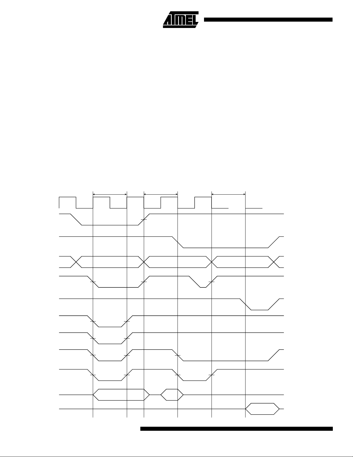
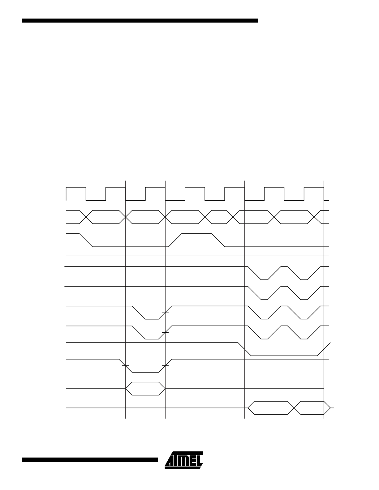
Figure 3 shows a write to memory 0, followed by a write
and a read to memory 1. SMC_CSR0 is programmed for
one wait state with BAT = 0 and DFT = 0. SMC_CSR1 is
programmed for zero wait states with BAT = 1 and
DFT = 0. SMC_MCR is programmed for early reads from
all memories.
The write to memory 0 is a 32-bit word access and, therefore, all four NWE strobes are active. As BAT = 0, they are
configured as write strobes and have the same timing as
NWR. As the access employs a single wait state, the write
strobe pulse is one clock cycle long.
There is a chip select change wait state between the memory 0 write and the memory 1 write. The new address is
output at the end of the memory 0 access but the strobes
are delayed for one clock cycle.
The write to memory 1 is a half-word (16-bit) access to an
odd half-word address and, therefore, NWE2 and NWE3
are active. As BAT = 1 they are configured as byte-select
Figure 3. Write to Memory 0, Write and Read to Memory 1
BCLK
signals and have the same timing as NCE. As the access
has no internal wait states, the write strobe pulse is onehalf clock cycle long. Data and address are driven until the
write strobe rising edge is sensed at the SIAP pin to guarantee positive hold times.
There is an early read wait state between the memory 1
write and the memory 1 read to provide time for the
AT75C310 to disable the output data before the memory is
read. If the read was normal mode, i.e., not early, the
NSOE strobe would not fall until the rising edge of BCLK
and no wait state would be inserted. If the write and early
read were to different memories, then the early read wait
state is not required as a chip select wait state will be
implemented.
The read from memory 1 is a byte access to an address
with a byte offset of two and, therefore, only NWE2 is
active.
NCE0
NCE1
NWR
NSOE
NWE0
NWE1
NWE2
NWE3
A
22
D (SIAP)
D (MEM)
AT75C310
Page 23
AT75C310
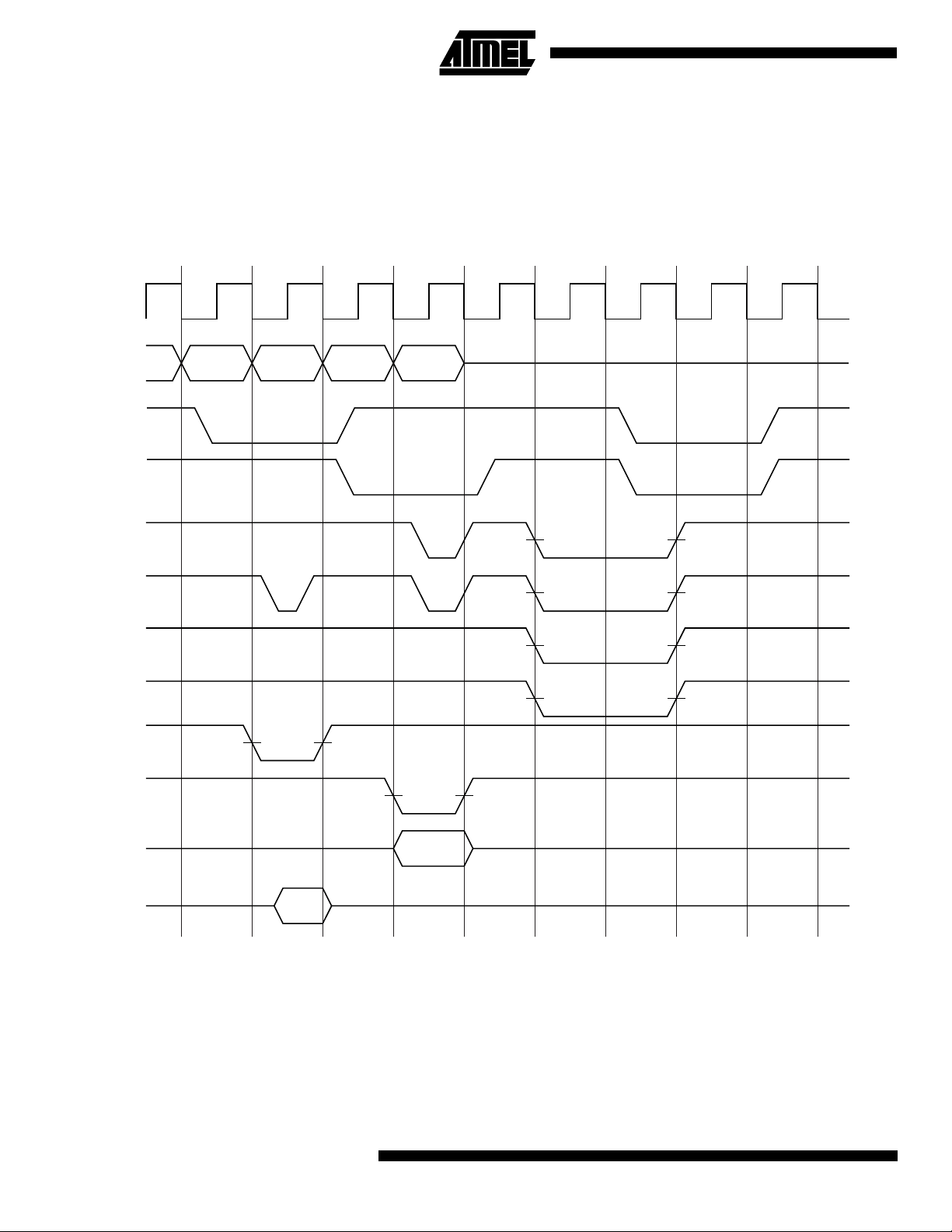
Figure 4 shows a write and a read to memory 0, followed
by a read and a write to memory 1. SMC_CSR0 is programmed for zero wait states with BAT = 0 and DFT = 0.
SMC_CSR1 is programmed for zero wait states with
BAT = 1 and DFT = 1. SMC_MCR is programmed for normal reads from all memories
The write to memory 0 is a byte access and, therefore, only
one NWE strobe is active. As BAT = 0, they are configured
as write strobes and have the same timing as NWR.
The memory 0 read immediately follows the write as early
reads are not configured and an early read wait state is not
required. As early reads are not configured, the read strobe
pulse is one-half clock cycle long.
output at the end of the memory 0 access but the strobes
are delayed for one clock cycle.
The write to memory 1 is a half-word (16-bit) access to an
even half-word address and, therefore, NWE0 and NWE1
are active. As BAT = 1, they are configured as byte select
signals and have the same timing as NCE.
As DFT = 1 for memory 1, a wait state is implemented
between the read and write to provide time for the memory
to stop driving the data bus. DFT wait states are only implemented at the end of read accesses.
The read from memory 1 is a byte access to an address
with a byte offset of two and, therefore, only NWE2 is
active.
There is a chip select change wait state between the memory 0 write and the memory 1 read. The new address is
Figure 4. Write and Read to Memory 0, Read and Write to Memory 1
Chip Select
Wait State
BCLK
NCE0
Data Float
Wait State
NCE1
NWR
NSOE
NWE0
NWE1
NWE2
NWE3
D (SIAP)
A
D (MEM)
23
Page 24

DMC: Dynamic Memory Controller
The ARM can access external DRAM by means of the
DRAM memory controller. The DMC sits on the ASB bus
and provides a glueless memory interface to external EDO
DRAM using the common address and data buses.
The AT75C310 supports two DRAM memory regions, each
with its own RAS signal. Both DRAM regions share the
same CAS, OE, WE, address and data signals.
The DRAM controller is programmed as an internal peripheral that has a standard APB bus interface and a set of
memory-mapped registers.
The DMC is designed to operate with extended data-out
(EDO) DRAM. It supports two 16-MByte address spaces
and a programmable 16- or 32-bit data bus. The controller
multiplexes the processor address to form DRAM row and
column addresses. The row and column addresses can be
configured to support various combinations of DRAM memory size, page size and data bus width.
The DMC supports:
• One or two DRAM memory regions
• DRAM memory region size of 2, 4, 8 or 16 megabytes
• DRAM page size of 256, 512, 1024 or 2048 columns
• Up to 15 row- and 11 column-address bits
• Asymmetric row and column addressing
• 16- or 32-bit DRAM data bus
• Automatic page breaking of burst accesses
• Automatic CAS-before-RAS refresh on timer trigger
• Automatic power-up initialization sequence
DMC Operation
The DMC multiplexes the ASB address to DRAM row and
column addresses. The column address must be between
eight and eleven bits. The row address is the required number of higher-order bits to support all combinations of permitted page- and memory-region sizes and both data bus
widths.
The DMC automatically inserts precharge and RAS cycles
and supplies an updated row address to the DRAM when a
sequential burst access from an ASB bus master crosses a
DRAM page boundary. The necessary number of wait
states is inserted to hold the bus master during the pre-
charge and RAS cycles.
The DMC performs a CAS-before-RAS refresh cycle on
both DRAM memory regions on the rising edge of a trigger
signal from the AT75C310 on-chip timer. If the DMC is per-
forming a DRAM access when the trigger occurs, the
access will finish before the refresh operation is performed.
In the case of a burst access, the refresh is not performed
until the end of the burst.
The DMC is capable of limiting the length of a burst access
if a refresh trigger has been received. If the feature is
enabled, the DMC performs the refresh operation once it
has been pending for 32 accesses in a burst sequence.
The DMC includes the functionality to interface the 32-bit
ASB data bus with a 16-bit DRAM data bus. It automatically
performs two accesses to the DRAM to service a 32-bit
access from the ASB.
Initialization Sequence
The DMC performs eight CAS-before-RAS refresh opera-
tions to both DRAM banks at the end of the AT75C310
reset pulse. The processor is not required to perform any
DRAM initialization operations. However, it is required to
initialize the DMC.
Data Alignment
The DMC only supports accesses to the appropriate data
boundary, i.e., word accesses must be word-aligned and
half-word accesses must be half-word-aligned. Misaligned
accesses will be ignored by the DMC, and the AMBA
decoder will therefore flag an abort to the appropriate ASB
bus master.
The ARM processor does not guarantee the level of the
bottom two address bits for an instruction access in ARM
state or the bottom address bit for an instruction fetch in
Thumb state. Therefore, the DMC will service misaligned
instruction fetches and force alignment, e.g., a 16-bit
instruction fetch from address 0x00000003 is performed as
a 16-bit read of address 0x00000002.
Table 9. DMC Register Map
Register Offset Register Description Register Name Access
0x0
0x4
0x8
24
DRAM Region 0 Configuration Register
DRAM Region 1 Configuration Register
DRAM Common Configuration Register
AT75C310
DMC_MR0 Read/write
DMC_MR1 Read/write
DMC_CR Read/write
Page 25
AT75C310
DRAM Memory Region Configuration Register
For each of the two DRAM memory regions there is a memory-mapped register.
Register Name: DMC_MR0..DMC_MR1
Reset value of DMC_MR0 is 0x40000000; reset value of DMC_MR1 is 0x50000000
31 30 29 28 27 26 25 24
BA
23 22 21 20 19 18 17 16
BA –––––
15 14 13 12 11 10 9 8
––––––––
76543210
––– SZ PS EMR
• EMR: Enable Memory Region
When low, the memory region is not enabled; any access to this region will generate an abort.
• PS: Page Size
This field should be set to the number of column address lines that are required by the external DRAM. It also indicates
the number of columns per page. The controller breaks sequential bursts on page boundaries.
PS Columns No. Column Address LInes
00
01
10
1 1
256 8
512 9
1024 10
2048 11
• SZ: Size
This field indicates the size of the memory region.
SZ Size of Memory Region
00 2 MB
01 4 MB
10 8 MB
1 1 16 MB
• BA: Base Address
This field indicates the base address of the memory region. It should be programmed with the top 11 bits of the
required base address. The number of bits used for address decoding is dependent on the SZ field.
SZ BA Bits Used
2 MB BA[31:21]
4 MB BA[31:22]
8 MB BA[31:23]
16 MB BA[31:24]
25
Page 26
DRAM Common Configuration Register (DMC_CR)
The Common Configuration Register defines parameters which are common to the two DRAM regions.
Register Name: DMC_CR
Reset Value is 0x00000000
31 30 29 28 27 26 25 24
––––––––
23 22 21 20 19 18 17 16
––––––––
15 14 13 12 11 10 9 8
––––––––
76543210
–––––ROR BBR DBW
• DBW: Data Bus Width
When high, the DRAM data bus is 32 bits wide. When low, the DRAM data bus is only 16 bits wide. The DMC splits 32bit transfers into two 16-bit transfers which are transparent to the ASB.
• BBR: Break Burst for Refresh
When this flag is high, the controller breaks long burst accesses every 32 CAS cycles if a refresh cycle is pending in
order to allow the refresh cycle to be performed. This prevents excessively long bursts from delaying refresh cycles.
• ROR: RAS-only Refresh
When high, the CAS signal is held inactive (high) during normal DRAM accesses, thereby generating a RAS-only
Refresh cycle. This feature allows software to generate the row address and initiate the refresh cycle. When low, memory operations behave as normal and CAS is not inhibited.
DRAM Interface
Table 10. DRAM Interface
FPDRAM Description Type Notes
NRAS[1:0]
NCAS[3:0]
NWE
NOE
A[14:0]
D[31:0]
Row Address Strobe O
Column Address
Strobe
Write Enable O
Output Enable O
Address Bus O
Data Bus I/O
O
One strobe per DRAM region. Common to four bytes in each region
One strobe per byte. Common to both DRAM regions. Only NCAS[1:0] used
when Data Bus Width is 16
Common to both regions
Common to both regions
Multiplexed row and column addresses
D[15:0] used when Data Bus Width is 16
26
AT75C310
Page 27
Dynamic Memory Accesses
Figure 5 and Figure 6 describe the different bus operations
that can be performed by DMC.
Write Access Followed by Burst Read Access
Figure 5 shows a write to DRAM0 followed by a burst of
two reads from the same device.
The write access takes two clock cycles. During the first
cycle, the row address is output and the RAS strobe is
asserted. In the next cycle, the column address is output
and the CAS strobes are asserted. The read is a half-word
(16-bit) access to an odd half-word address so only CAS2
and CAS3 are active.
Figure 5. Write to DRAM0 Waveform
BCLK
AT75C310
The read access is not sequential to the write access
(regardless of the addresses) and the RAS strobe is there-
fore raised for a precharge cycle between the accesses.
The read accesses take two clock cycles to read the first
word of data and one additional clock cycle for the second
word. The row address and RAS are asserted in the same
manner as for the read access. The column address and
CAS strobes are asserted earlier for a read access than for
a write access in order to provide time for the data to read
the processor core. The read accesses shown are word
(32-bit) accesses and all four CAS strobes are therefore
active.
The DMC asserts BWAIT to the ARM during the row
address and precharge cycles.
RAS0
RAS1
CAS0
CAS1
CAS2
CAS3
NDOE
NDWE
D (SIAP)
A
D (MEM)
27
Page 28
Read and Write Accesses Followed by CAS before RAS Refresh
Figure 6 shows a read access followed by a write. As the
accesses are to different devices, there is no need for a
precharge cycle.
Figure 6. Read Access Followed by a Write
BCLK
A
RAS0
RAS1
CAS0
The read is a byte access (one CAS strobe is active) and
the write is a half-word access (two CAS strobes are
active).
The CAS before RAS refresh cycle refreshes all DRAM
devices controlled by the DMC. All RAS and CAS strobes
are therefore active.
CAS1
CAS2
CAS3
NDOE
NDWE
D (SIAP)
D (MEM)
28
AT75C310
Page 29
AIC: Advanced Interrupt Controller
The AT75C310 has an eight-level priority, individually
maskable interrupt controller. This feature substantially
reduces the software and real-time overhead in handling
internal and external interrupts.
The interrupt controller is connected to the NFIQ (fast interrupt request) and the NIRQ (standard interrupt request)
inputs of the ARM7TDMI processor. The processor’s NFIQ
line can only be asserted by the external fast interrupt
request input FIQ. The NIRQ line can be asserted by the
interrupts generated by the on-chip peripherals and the
external interrupt request lines IRQ0 and FIQ.
Figure 7. Interrupt Controller Block Diagram
AT75C310
The eight-level priority encoder allows the customer to
define the priority between the different NIRQ interrupt
sources.
Internal sources are programmed to be level-sensitive or
edge-triggered. External sources can be programmed to be
positive- or negative-edge triggered or high- or low-level
sensitive.
The interrupt sources are listed in Table 11 and the AIC
programmable registers in Table 12.
FIQ Source
Advanced Peripheral
Bus (APB)
Internal Interrupt Sources
External Interrupt Sources
Note: After a hardware reset, the AIC pins are controlled by the PIO controller. They must be configured to be controlled by the periph-
eral before being used.
Memorization
Control
Logic
Memorization
Prioritization
Controller
NFIQ
Manager
NIRQ
Manager
NFIQ
ARM7TDMI
Core
NIRQ
29
Page 30

Table 11. AIC Interrupt Sources
Interrupt Source Interrupt Name Interrupt Description
0 FIQ/LOWP
1 WDIRQ
2SWIRQ
3UAIRQ
4TC0IRQ
5TC1IRQ
6TC2IRQ
7PIOAIRQ
8 LCDIRQ
9 SPIIRQ
10 IRQ0
11 –
12 OAKIRQ
13 OAKBIRQ
14 UBIRQ
15 PIOBIRQ
16 –
17 –
18 –
19 –
20 –
21 –
22 –
23 –
24 –
25 –
26 –
27 –
28 –
29 –
30 –
31 –
Fast interrupt (external), low-power
Watchdog
Software (Generated by AIC)
USART A
Timer/Counter0
Timer/Counter1
Timer/Counter2
PIO A
LCD Controller
SPI
External 0
Reserved
OAK A Semaphore
OAK B Semaphore
USART B
PIO B
Reserved
Reserved
Reserved
Reserved
Reserved
Reserved
Reserved
Reserved
Reserved
Reserved
Reserved
Reserved
Reserved
Reserved
Reserved
Reserved
30
AT75C310
Page 31

AT75C310
Priority Controller
The NIRQ line is controlled by an eight-level priority
encoder. Each source has a programmable priority level of
7 to 0. Level 7 is the highest priority and level 0 the lowest.
When the AIC receives more than one unmasked interrupt
at a time, the interrupt with the highest priority is serviced
first. If both interrupts have equal priority, the interrupt with
the lowest interrupt source number is serviced first. Interrupt source numbers are given in Table 11.
The current priority level is defined as the priority level of
the current interrupt at the time the register AIC_IVR is
read (the interrupt which will be serviced).
If a higher priority unmasked interrupt occurs and an interrupt already exists, there are two possible outcomes
depending on whether the AIC_IVR has been read.
1. If the NIRQ line has been asserted but the AIC_IVR
has not been read, then the processor will read the
new higher priority interrupt handler address in the
AIC_IVR register and the current interrupt level is
updated.
2. If the processor has already read the AIC_IVR, then
the NIRQ line is reasserted. When the processor
has authorized nested interrupts to occur and reads
the AIC_IVR again, it reads the new, higher-priority
interrupt handler address. At the same time, the
current priority value is pushed onto a first-in lastout stack and the current priority is updated to the
higher priority.
When the End of Interrupt Command Register
(AIC_EOICR) is written, the current interrupt level is
updated with the last stored interrupt level from the stack (if
any). Hence, at the end of a higher priority interrupt, the
AIC returns to the previous state corresponding to the preceding lower priority interrupt which had been interrupted.
Interrupt Handling
The interrupt handler must read the AIC_IVR as soon as
possible. This de-asserts the NIRQ request to the processor and clears the interrupt in case it is programmed to be
edge-triggered. This permits the AIC to assert the NIRQ
line again when a higher-priority unmasked interrupt
occurs.
At the end of the interrupt service routine, the End of Interrupt Command Register (AIC_EOICR) must be written.
This allows pending interrupts to be serviced.
Interrupt Masking
Each interrupt source, including FIQ, can be enabled or
disabled using the command registers AIC_IECR and
AIC_IDCR. The interrupt mask can be read in the read-only
register AIC_IMR. A disabled interrupt does not affect the
servicing of other interrupts.
Interrupt Clearing and Setting
All interrupt sources which are programmed to be edge-
triggered (including FIQ) can be individually set or cleared
by writing to the registers AIC_ISCR and AIC_ICCR,
respectively. This function of the interrupt controller is avail-
able for auto-test or software debug purposes.
Fast Interrupt Request
The external FIQ line is the only source which can raise a
fast interrupt request to the processor. Therefore, it has no
priority controller.
The external FIQ line can be programmed to be positive- or
negative-edge triggered or high- or low-level sensitive in
the AIC_SMR0 register.
The interrupt handler can be stored starting from address
0x0000001C as described in the Atmel ARM7TDMI
datasheet, literature number 0673.
Software Interrupt
Interrupt source 1 of the AIC is a software interrupt. It must
be programmed to be edge-triggered in order to set or clear
it by writing to the AIC_ISCR and AIC_ICCR.
This is independent of the SWI instruction of the
ARM7TDMI processor.
Standard Interrupt Sequence
The following conditions are assumed:
• The AIC has been programmed and interrupts are
enabled.
• The instruction at address 0x18 (IRQ exception vector
address) jumps into a default handler which reads
AIC_IVR and then jumps to the specific service routine
for the read interrupt number.
When NIRQ is asserted, if the bit “I” of CPSR is 0, the
sequence is:
1. The CPSR is stored in SPSR_irq, the current value
of the Program Counter is loaded in the IRQ link
register (R14_irq) and the Program Counter (R15)
is loaded with 0x18. In the following cycle during
fetch at address 0x1C, the ARM core adjusts
R14_irq, decrementing it by 4.
2. The ARM core enters IRQ mode if it is not already.
3. When the instruction at 0x18 is executed, the Program Counter is loaded with the start address of the
default interrupt handler.
4. The previous interrupt priority level is stored onto a
stack. Note that if no interrupt was active, the previous interrupt priority will be zero.
5. The AIC_IVR register is read causing the IRQ
request to be cancelled and the current interrupt priority is updated. Any registers that may be used can
be stored onto the stack at this point if required. The
31
Page 32

code then checks the interrupt number and
branches to the required service routine.
6. The service routine should start by saving the Link
Register (R14_irq) and the SPSR (SPSR_irq). Note
that the Link Register must be decremented by four
when it is saved if it is to be restored directly into the
Program Counter at the end of the interrupt. Alternatively, this can be done at the start of the default
handler.
7. Further interrupts can then be unmasked by clearing the “I” bit in the CPSR, allowing re-assertion of
the NIRQ to be taken into account by the core. This
occurs if an interrupt with a higher priority than the
current one occurs.
8. The Interrupt Handler then proceeds as required,
saving the registers which will be used and restoring them at the end. During this phase, an interrupt
of priority higher than the current level restarts the
sequence from step 1. Note that if the interrupt is
programmed to be level sensitive, the source of the
interrupt must be cleared during this phase.
9. The “I” bit in the CPSR must be set in order to mask
interrupts before exiting to ensure that the interrupt
is completed in an orderly manner.
10. The service routine should then branch to the common exit routine.
11. The stored priority level is fetched (from a stack)
and witten to the End Of Interrupt Command Register (AIC_EOICR) in order to indicate to the AIC that
the current interrupt is finished. This restores the
previous current level if one existed. If another interrupt is pending with lower or equal priority than the
old current level but with higher priority than the new
current level, the NIRQ line is re-asserted. The
interrupt sequence does not immediately start
because the “I” bit is set in the core.
12. The SPSR (SPSR_irq) is restored. Finally, the
saved value of the Link Register is restored directly
into the PC. This has the effect of returning from the
interrupt to whatever was being executed before
and of loading the CPSR with the stored SPSR,
masking or unmasking the interrupts depending on
the state saved in the SPSR (the previous state of
the ARM core).
Note that the “I” bit in the SPSR is significant. If it is set, it
indicates that the ARM core was just about to mask IRQ
interrupts when the mask instruction was interrupted.
Hence, when the SPSR is restored, the mask instruction is
completed (IRQ is masked).
Fast Interrupt Sequence
It is assumed that:
• The AIC has been programmed and the fast interrupt is
enabled.
• The instruction at address 0x1C (FIQ exception vector
address) is a branch to an FIQ service routine or the first
instruction of the FIQ routine
Nested fast interrupts are not needed by the user.
When NFIQ is asserted, if the bit “F” of CPSR is 0, the
sequence is:
1. The CPSR is stored in SPSR_fiq, the current value
of the Program Counter is loaded in the FIQ link
register (R14_fiq) and the Program Counter (R15) is
loaded with 0x1C. In the following cycle, during
fetch at address 0x20, the ARM core adjusts
R14_fiq, decrementing it by four.
2. The ARM core enters FIQ mode and starts execut-
ing the instruction at address 0x1c, which may be a
branch or the first service routine instruction.
3. The AIC_FVR register is read. This results in the
cancellation of the FIQ request and returns 0x0.
4. The previous step has the effect of branching to the
corresponding interrupt service routine. It is not
necessary to save the Link Register (R14_fiq) and
the SPSR (SPSR_fiq) if nested fast interrupts are
not needed.
5. The Interrupt Handler then proceeds as required. It
is not necessary to save registers R8 to R13
because FIQ mode has its own dedicated registers
and the user R8 to R13 are banked. The other registers, R0 to R7, must be saved before being used,
and restored at the end (before the next step). Note
that if the fast interrupt is programmed to be level
sensitive, the source of the interrupt must be
cleared during this phase in order to de-assert the
NFIQ line.
6. Finally, the Link Register (R14_fiq) is restored into
the PC after decrementing it by 4 (with instruction
sub pc, lr, #4 for example). This has the effect of
returning from the interrupt to whatever was being
executed before, and of loading the CPSR with the
SPSR, masking or unmasking the fast interrupt
depending on the state saved in the SPSR.
Note that the “F” bit in the SPSR is significant. If it is set, it
indicates that the ARM core was just about to mask FIQ
interrupts when the mask instruction was interrupted.
Hence, when the SPSR is restored, the interrupted instruction is completed (FIQ is masked).
32
AT75C310
Page 33

AT75C310
AIC User Interface
Base Address: 0xFF030000
Table 12. AIC Memory Map
Offset Register Description Register Name Access Reset State
0x000
0x004
–––Read/write 0
0x07C
0x080
0x084
–
0x0FC
0x100
0x104
0x108
0x10C
0x110
0x114
0x118
0x11C
Source Mode Register 0
Source Mode Register 1
Source Mode Register 31
Reserved
Reserved
Reserved
Reserved
IRQ Vector Register
FIQ Vector Register
Interrupt Status Register
Interrupt Pending Register
Interrupt Mask Register
Core Interrupt Status Register
Reserved
Reserved
AIC_SMR0 Read/write 0
AIC_SMR1 Read/write 0
AIC_SMR31 Read/write 0
–––
–––
–––
–––
AIC_IVR Read-only 0
AIC_FVR Read-only 0
AIC_ISR Read-only 0
AIC_IPR Read-only (see Note 1)
AIC_IMR Read-only 0
AIC_CISR Read-only 0
–––
–––
0x120
0x124
0x128
0x12C
0x130
Note: 1. The reset value of this register depends on the level of the external IRQ lines. All other sources are cleared at reset.
Interrupt Enable Command Register
Interrupt Disable Command Register
Interrupt Clear Command Register
Interrupt Set Command Register
End of Interrupt Command Register
AIC_IECR Write-only –
AIC_IDCR Write-only –
AIC_ICCR Write-only –
AIC_ISCR Write-only –
AIC_EOICR Write-only –
33
Page 34

AIC Source Mode Register
Register Name: AIC_SMR0..AIC_SMR31
Access Type: Read/write
Reset Value: 0
31 30 29 28 27 26 25 24
––––––––
23 22 21 20 19 18 17 16
––––––––
15 14 13 12 11 10 9 8
––––––––
76543210
– SRCTYPE –– PRIOR
• PRIOR: Priority Level
Programs the priority level for all sources except source 0 (FIQ).
The priority level can be between 0 (lowest) and 7 (highest).
The priority level is not used for the FIQ in the SMR0.
• SRCTYPE: Interrupt Source Type
Programs the input to be positive- or negative-edge triggered or positive- or negative-level sensitive.
The active level or edge is not programmable for the internal sources.
SRCTYPE Internal Sources External Sources
00
01
10
11
Level-sensitive Low-level sensitive
Edge-triggered Negative-edge triggered
Level-sensitive High-level sensitive
Edge-triggered Positive-edge triggered
AIC Interrupt Vector Register
Register Name: AIC_IVR
Access Type: Read-only
Reset Value: 0
31 30 29 28 27 26 25 24
––––––––
23 22 21 20 19 18 17 16
––––––––
15 14 13 12 11 10 9 8
––––––––
76543210
PRIOR IRQID
• PRIOR
Interrupt priority
• IRQID
Active interrupt number. Used to select required service routine.
34
AT75C310
Page 35
AIC FIQ Vector Register
Register Name: AIC_FVR
Access Type: Read-only
Reset Value: 0
31 30 29 28 27 26 25 24
23 22 21 20 19 18 17 16
15 14 13 12 11 10 9 8
76543210
• FIQV: FIQ Vector Register
FIQ = 0x00000000 if FIQ active
FIQ = 0xFFFFFFFF otherwise
AIC Interrupt Status Register
Register Name: AIC_ISR
Access Type: Read-only
Reset Value: 0
AT75C310
FIQV
FIQV
FIQV
FIQV
31 30 29 28 27 26 25 24
––––––––
23 22 21 20 19 18 17 16
––––––––
15 14 13 12 11 10 9 8
––––––––
76543210
PRIOR IRQID
• PRIOR
Interrupt priority
• IRQID
Active interrupt number. Used to select required service routine.
35
Page 36

AIC Interrupt Pending Register
Register Name: AIC_IPR
Access Type: Read-only
Reset Value: Undefined
31 30 29 28 27 26 25 24
––––––––
23 22 21 20 19 18 17 16
––––––––
15 14 13 12 11 10 9 8
PIOBIRQ UBIRQ OAKBIRQ OAKAIRQ – IRQ0 SPIIRQ LCDIRQ
76543210
PIOAIRQ TC2IRQ TC1IRQ TC0IRQ UAIRQ SWIRQ WDIRQ FIQ
• Interrupt Pending
0 = Corresponding interrupt is inactive
1 = Corresponding interrupt is pending
AIC Interrupt Mask Register
Register Name: AIC_IMR
Access Type: Read-only
Reset Value: 0
31 30 29 28 27 26 25 24
––––––––
23 22 21 20 19 18 17 16
––––––––
15 14 13 12 11 10 9 8
PIOBIRQ UBIRQ OAKBIRQ OAKAIRQ – IRQ0 SPIIRQ LCDIRQ
76543210
PIOAIRQ TC2IRQ TC1IRQ TC0IRQ UAIRQ SWIRQ WDIRQ FIQ
• Interrupt Mask
0 = Corresponding interrupt is disabled
1 = Corresponding interrupt is enabled
36
AT75C310
Page 37

AIC Core Interrupt Status Register
Register Name: AIC_CISR
Access Type: Read-only
Reset Value: 0
31 30 29 28 27 26 25 24
––––––––
23 22 21 20 19 18 17 16
––––––––
15 14 13 12 11 10 9 8
––––––––
76543210
––––––NIRQ NFIQ
• NFIQ: NFIQ Status
0 = NFIQ line inactive
1 = NFIQ line active
• NIRQ: NIRQ Status
0 = NIRQ line inactive
1 = NIRQ line active
AT75C310
AIC Interrupt Enable Command Register
Register Name: AIC_IECR
Access Type: Write-only
31 30 29 28 27 26 25 24
––––––––
23 22 21 20 19 18 17 16
––––––––
15 14 13 12 11 10 9 8
––––––––
76543210
––––––NIRQ NFIQ
• NFIQ: NFIQ Status
0 = NFIQ line inactive
1 = NFIQ line active
• NIRQ: NIRQ Status
0 = NIRQ line inactive
1 = NIRQ line active
37
Page 38

AIC Interrupt Disable Command Register
Register Name: AIC_IDCR
Access Type: Write-only
31 30 29 28 27 26 25 24
––––––––
23 22 21 20 19 18 17 16
––––––––
15 14 13 12 11 10 9 8
––––––––
76543210
––––––NIRQ NFIQ
• NFIQ: NFIQ Status
0 = NFIQ line inactive
1 = NFIQ line active
• NIRQ: NIRQ Status
0 = NIRQ line inactive
1 = NIRQ line active
AIC Interrupt Clear Command Register
Register Name: AIC_ICCR
Access Type: Write-only
31 30 29 28 27 26 25 24
––––––––
23 22 21 20 19 18 17 16
––––––––
15 14 13 12 11 10 9 8
––––––––
76543210
––––––NIRQ NFIQ
• NFIQ: NFIQ Status
0 = NFIQ line inactive
1 = NFIQ line active
• NIRQ: NIRQ Status
0 = NIRQ line inactive
1 = NIRQ line active
38
AT75C310
Page 39

AIC Interrupt Set Command Register
Register Name: AIC_ISCR
Access Type: Write-only
31 30 29 28 27 26 25 24
––––––––
23 22 21 20 19 18 17 16
––––––––
15 14 13 12 11 10 9 8
––––––––
76543210
––––––NIRQ NFIQ
• NFIQ: NFIQ Status
0 = NFIQ line inactive
1 = NFIQ line active
• NIRQ: NIRQ Status
0 = NIRQ line inactive
1 = NIRQ line active
AT75C310
AIC End of Interrupt Command Register
Register Name: AIC_EOICR
Access Type: Write-only
31 30 29 28 27 26 25 24
––––––––
23 22 21 20 19 18 17 16
––––––––
15 14 13 12 11 10 9 8
––––––––
76543210
––––––––
The End of Interrupt Command Register is used by the interrupt routine to indicate that the interrupt handling is complete.
Any value can be written because it is only necessary to make a write to this register location to signal the end of interrupt
handling. The value written is taken by the AIC and used as the new interrupt priority level, i.e., if no interrupt was active
when the current routine was entered, zero is written. If an interrupt was active and interrupt nesting is enabled, the value
written should be the priority and interrupt number of the previous interrupt.
39
Page 40

PIO: Parallel I/O Controller
The AT75C310 has 23 programmable I/O lines. Three pins
on the AT75C310 are dedicated as general-purpose I/O
pins. Other I/O lines are multiplexed with an external signal
of a peripheral to optimize the use of available package
pins. Refer to Table 13 and Table 14 on page 42. These
lines are controlled by two separate and identical PIO controllers, PIO A and PIO B. Each PIO controller also provides an internal interrupt signal to the AIC.
Multiplexed I/O Lines
Most I/O lines are multiplexed with an I/O signal of a
peripheral. After reset, the pin is controlled by the PIO controller and is in input mode.
When a peripheral signal is not used in an application, the
corresponding pin can be used as a parallel I/O. Each parallel I/O line is bi-directional, whether the peripheral defines
the signal as input or output. Figure 8 shows the multiplexing of the peripheral signals with parallel I/O signals.
If a pin is multiplexed between the PIO controller and a
peripheral, the pin is controlled by the registers PIO_PER
(PIO Enable) and PIO_PDR (PIO Disable). The register
PIO_PSR (PIO Status) indicates whether the pin is controlled by the corresponding peripheral or by the PIO controller.
If a pin is a general-purpose parallel I/O pin (not multiplexed with a peripheral), PIO_PER and PIO_PDR have no
effect and PIO_PSR returns 1 for the bits corresponding to
these pins.
When the PIO is selected, the peripheral input line is connected to zero.
Output Selection
The user can enable each individual I/O signal as an output
with the registers PIO_OER (Output Enable) and
PIO_ODR (Output Disable). The output status of the I/O
signals can be read in the register PIO_OSR (Output Status). The direction defined has an effect only if the pin is
configured to be controlled by the PIO controller.
I/O Levels
Each pin can be configured to be driven high or low. The
level is defined in four different ways, according to the following conditions:
1. If a pin is controlled by the PIO Controller and is
defined as an output (see “Output Selection”
above), the level is programmed using the registers
PIO_SODR (Set Output Data) and PIO_CODR
(Clear Output Data). In this case, the programmed
value can be read in PIO_ODSR (Output Data
Status).
2. If a pin is controlled by the PIO controller and is not
defined as an output, the level is determined by the
external circuit.
3. If a pin is not controlled by the PIO controller, the
state of the pin is defined by the peripheral.
4. In all cases, the level on the pin can be read in the
register PIO_PDSR (Pin Data Status).
Filters
Optional input glitch filtering is available on each pin and is
controlled by the registers PIO_IFER (Input Filter Enable)
and PIO_IFDR (Input Filter Disable). Input glitch filtering
can be selected whether the pin is used for its peripheral
function or as a parallel I/O line. The register PIO_IFSR
(Input Filter Status) indicates whether or not the filter is
activated for each pin.
Interrupts
Each parallel I/O can be programmed to generate an interrupt when a level change occurs. This is controlled by the
PIO_IER (Interrupt Enable) and PIO_IDR (Interrupt Disable) registers which enable/disable the I/O interrupt by
setting/clearing the corresponding bit in the PIO_IMR.
When a change in level occurs, the corresponding bit in the
PIO_ISR (Interrupt Status) is set whether the pin is used as
a PIO or a peripheral and whether it is defined as input or
output. If the corresponding interrupt in PIO_IMR (Interrupt
Mask) is enabled, the PIO interrupt is asserted.
When PIO_ISR is read, the register is automatically
cleared.
User Interface
Each individual I/O is associated with a bit position in the
Parallel I/O User Interface Registers. Each of these registers is 32 bits wide. If a parallel I/O line is not defined, writing to the corresponding bits has no effect. Undefined bits
read as zero.
40
AT75C310
Page 41

Figure 8. Parallel I/O Multiplexed with a Bi-directional Signal
AT75C310
PIO_OSR
Pad
Pad Output Enable
Pad Output
Pad Input
PIO_PSR
1
0
1
0
0
1
PIO_PSR
PIO_PDSR
Peripheral
Output
Enable
PIO_ODSR
Peripheral
Output
Peripheral
Input
Event
Detection
PIO_ISR
PIO_IMR
PIOIRQ
41
Page 42

Table 13. PIO Controller A Connection Table
PIO Controller A Peripheral
Bit
(1)
Number
0 PA0 OAKAIN0
1 PA1 OAKAIN1
2PA2OAKAOUT0
3PA3OAKAOUT1
4 PA4 OAKBIN0
5 PA5 OAKBIN1
6 PA6 OAKBOUT0
7 PA7 OAKBOUT1
8PA8TCLK0
9PA9TIOA0
10 PA10 TIOB0
11 PA11 SCLKA
12 PA12 NPCS1
Note: 1. Bit number refers to the data bit which corresponds to this signal in each of the User Interface registers.
Port Name Port Name Signal Description Signal Direction
OakDSPCore A User Input Input
OakDSPCore A User Input Input
OakDSPCore A User Output Output
OakDSPCore A User Output Output
OakDSPCore B User Input Input
OakDSPCore B User Input Input
OakDSPCore B User Output Output
OakDSPCore B User Output Output
Timer 0 External Clock Input
Timer 0 Signal A Input/Output
Timer 0 Signal B Input/Output
Serial Clock Input/Output
Optional SPI Chip Select 1 Output
Reset State
PIO 71
PIO 72
PIO 73
PIO 74
PIO 77
PIO 78
PIO 79
PIO 80
PIO 82
PIO 83
PIO 85
PIO 86
PIO 88
Pin
Number
Table 14. PIO Controller B Connection Table
PIO Controller B Peripheral
Bit
(1)
Number
0 PB0 TCLK1 Timer 1 External Clock Input PIO 55
1 PB1 TIOA1 Timer 1 Signal A Input/Output PIO 53
2 PB2 TIOB1 Timer 1 Signal B Input/Output PIO 51
3PB3 –– –PIO 47
4PB4 –– –PIO 44
5 PB5 NRIA Ring Indicator Input PIO 43
6 PB6 NWDOVF Watchdog Overflow Output PIO 42
7 PB7 NCE1 Chip Select Output PIO 38
8 PB8 NCE2 Chip Select Output PIO 54
9PB9 –– –PIO 52
Note: 1. Bit number refers to the data bit which corresponds to this signal in each of the User Interface registers.
Port Name Port Name Signal Description Signal Direction
Reset State
Pin
Number
42
AT75C310
Page 43

AT75C310
PIO User Interface
PIO Controller A Base Address: 0xFF00C000
PIO Controller B Base Address: 0xFF010000
Table 15. PIO Controller Memory Map
Offset Register Description Register Name Access Reset State
0x00 PIO Enable Register PIO_PER Write-only –
0x04 PIO Disable Register PIO_PDR Write-only –
0x08 PIO Status Register PIO_PSR Read-only –
0x0C Reserved –––
0x10 Output Enable Register PIO_OER Write-only –
0x14 Output Disable Register PIO_ODR Write-only –
0x18 Output Status Register PIO_OSR Read-only 0x0
0x1C Reserved –––
0x20 Input Filter Enable Register PIO_IFER Write-only –
0x24 Input Filter Disable Register PIO_IFDR Write-only –
0x28 Input Filter Status Register PIO_IFSR Read-only 0x0
0x2C Reserved –––
0x30 Set Output Data Register PIO_SODR Write-only –
0x34 Clear Output Data Register PIO_CODR Write-only –
0x38 Output Data Status Register PIO_ODSR Read-only 0x0
0x3C Pin Data Status Register PIO_PDSR Read-only See Note 1
0x40 Interrupt Enable Register PIO_IER Write-only –
0x44 Interrupt Disable Register PIO_IDR Write-only –
0x48 Interrupt Mask Register PIO_IMR Read-only –
0x4C Interrupt Status Register PIO_ISR Read-only See Note 2
Notes: 1. The reset value of this register depends on the level of the external pins at reset.
2. This register is cleared at reset. However, the first read of the register can give a value not equal to zero if any changes have
occurred on any pins between the reset and the read.
43
Page 44

PIO Enable Register
Register Name: PIO_PER
Access Type: Write-only
31 30 29 28 27 26 25 24
P31 P30 P29 P28 P27 P26 P25 P24
23 22 21 20 19 18 17 16
P23 P22 P21 P20 P19 P18 P17 P16
15 14 13 12 11 10 9 8
P15 P14 P13 P12 P11 P10 P9 P8
76543210
P7 P6 P5 P4 P3 P2 P1 P0
This register is used to enable individual pins to be controlled by the PIO controller instead of the associated peripheral.
When the PIO is enabled, the associated peripheral (if any) is held at logic zero.
1 = Enables the PIO to control the corresponding pin (disables peripheral control of the pin).
0 = No effect.
PIO Disable Register
Register Name: PIO_PDR
Access Type: Write-only
31 30 29 28 27 26 25 24
P31 P30 P29 P28 P27 P26 P25 P24
23 22 21 20 19 18 17 16
P23 P22 P21 P20 P19 P18 P17 P16
15 14 13 12 11 10 9 8
P15 P14 P13 P12 P11 P10 P9 P8
76543210
P7 P6 P5 P4 P3 P2 P1 P0
This register is used to disable PIO control of individual pins. When the PIO control is disabled, the normal peripheral function is enabled on the corresponding pin.
1 = Disables PIO control (enables peripheral control) on the corresponding pin.
0 = No effect.
44
AT75C310
Page 45

AT75C310
PIO Status Register
Register Name: PIO_PSR
Access Type: Read-only
31 30 29 28 27 26 25 24
P31 P30 P29 P28 P27 P26 P25 P24
23 22 21 20 19 18 17 16
P23 P22 P21 P20 P19 P18 P17 P16
15 14 13 12 11 10 9 8
P15 P14 P13 P12 P11 P10 P9 P8
76543210
P7 P6 P5 P4 P3 P2 P1 P0
This register indicates which pins are enabled for PIO control. This register is updated when PIO lines are enabled or disabled.
1 = PIO is active on the corresponding line (peripheral is inactive).
0 = PIO is inactive on the corresponding line (peripheral is active).
PIO Output Enable Register
Register Name: PIO_OER
Access Type: Write-only
31 30 29 28 27 26 25 24
P31 P30 P29 P28 P27 P26 P25 P24
23 22 21 20 19 18 17 16
P23 P22 P21 P20 P19 P18 P17 P16
15 14 13 12 11 10 9 8
P15 P14 P13 P12 P11 P10 P9 P8
76543210
P7 P6 P5 P4 P3 P2 P1 P0
This register is used to enable PIO output drivers. If the pin is driven by a peripheral, this has no effect on the pin, but the
information is stored. The register is programmed as follows:
1 = Enables the PIO output on the corresponding pin.
0 = No effect.
45
Page 46

PIO Output Disable Register
Register Name: PIO_ODR
Access Type: Write-only
31 30 29 28 27 26 25 24
P31 P30 P29 P28 P27 P26 P25 P24
23 22 21 20 19 18 17 16
P23 P22 P21 P20 P19 P18 P17 P16
15 14 13 12 11 10 9 8
P15 P14 P13 P12 P11 P10 P9 P8
76543210
P7 P6 P5 P4 P3 P2 P1 P0
This register is used to disable PIO output drivers. If the pin is driven by the peripheral, this has no effect on the pin, but the
information is stored. The register is programmed as follows:
1 = Disables the PIO output on the corresponding pin.
0 = No effect.
PIO Output Status Register
Register Name: PIO_OSR
Access Type: Read-only
Reset Value: 0
31 30 29 28 27 26 25 24
P31 P30 P29 P28 P27 P26 P25 P24
23 22 21 20 19 18 17 16
P23 P22 P21 P20 P19 P18 P17 P16
15 14 13 12 11 10 9 8
P15 P14 P13 P12 P11 P10 P9 P8
76543210
P7 P6 P5 P4 P3 P2 P1 P0
This register shows the PIO pin control (output enable) status which is programmed in PIO_OER and PIO ODR. The
defined value is effective only if the pin is controlled by the PIO. The register reads as follows:
1 = The corresponding PIO is output on this line.
0 = The corresponding PIO is input on this line.
46
AT75C310
Page 47

AT75C310
PIO Input Filter Enable Register
Register Name: PIO_IFER
Access Type: Write-only
31 30 29 28 27 26 25 24
P31 P30 P29 P28 P27 P26 P25 P24
23 22 21 20 19 18 17 16
P23 P22 P21 P20 P19 P18 P17 P16
15 14 13 12 11 10 9 8
P15 P14 P13 P12 P11 P10 P9 P8
76543210
P7 P6 P5 P4 P3 P2 P1 P0
This register is used to enable input glitch filters. It affects the pin whether or not the PIO is enabled. The register is programmed as follows:
1 = Enables the glitch filter on the corresponding pin.
0 = No effect.
PIO Input Filter Disable Register
Register Name: PIO_IFDR
Access Type: Write-only
31 30 29 28 27 26 25 24
P31 P30 P29 P28 P27 P26 P25 P24
23 22 21 20 19 18 17 16
P23 P22 P21 P20 P19 P18 P17 P16
15 14 13 12 11 10 9 8
P15 P14 P13 P12 P11 P10 P9 P8
76543210
P7 P6 P5 P4 P3 P2 P1 P0
This register is used to disable input glitch filters. It affects the pin whether or not the PIO is enabled. The register is programmed as follows:
1 = Disables the glitch filter on the corresponding pin.
0 = No effect.
47
Page 48
PIO Input Filter Status Register
Register Name: PIO_IFSR
Access Type: Read-only
Reset Value: 0
31 30 29 28 27 26 25 24
P31 P30 P29 P28 P27 P26 P25 P24
23 22 21 20 19 18 17 16
P23 P22 P21 P20 P19 P18 P17 P16
15 14 13 12 11 10 9 8
P15 P14 P13 P12 P11 P10 P9 P8
76543210
P7 P6 P5 P4 P3 P2 P1 P0
This register indicates which pins have glitch filters selected. It is updated when PIO outputs are enabled or disabled by
writing to PIO_IFER or PIO_IFDR.
1 = Filter is selected on the corresponding input (peripheral and PIO).
0 = Filter is not selected on the corresponding input.
PIO Set Output Data Register
Register Name: PIO_SODR
Access Type: Write-only
31 30 29 28 27 26 25 24
P31 P30 P29 P28 P27 P26 P25 P24
23 22 21 20 19 18 17 16
P23 P22 P21 P20 P19 P18 P17 P16
15 14 13 12 11 10 9 8
P15 P14 P13 P12 P11 P10 P9 P8
76543210
P7 P6 P5 P4 P3 P2 P1 P0
This register is used to set PIO output data. It affects the pin only if the corresponding PIO output line is enabled and if the
pin is controlled by the PIO. Otherwise, the information is stored.
1 = PIO output data on the corresponding pin is set.
0 = No effect.
48
AT75C310
Page 49

AT75C310
PIO Clear Output Data Register
Register Name: PIO_CODR
Access Type: Write-only
31 30 29 28 27 26 25 24
P31 P30 P29 P28 P27 P26 P25 P24
23 22 21 20 19 18 17 16
P23 P22 P21 P20 P19 P18 P17 P16
15 14 13 12 11 10 9 8
P15 P14 P13 P12 P11 P10 P9 P8
76543210
P7 P6 P5 P4 P3 P2 P1 P0
This register is used to clear PIO output data. It affects the pin only if the corresponding PIO output line is enabled and if the
pin is controlled by the PIO. Otherwise, the information is stored.
1 = PIO output data on the corresponding pin is cleared.
0 = No effect.
PIO Output Data Status Register
Register Name: PIO_ODSR
Access Type: Read-only
Reset Value: 0
31 30 29 28 27 26 25 24
P31 P30 P29 P28 P27 P26 P25 P24
23 22 21 20 19 18 17 16
P23 P22 P21 P20 P19 P18 P17 P16
15 14 13 12 11 10 9 8
P15 P14 P13 P12 P11 P10 P9 P8
76543210
P7 P6 P5 P4 P3 P2 P1 P0
This register shows the output data status which is programmed in PIO_SODR or PIO_CODR. The defined value is effective only if the pin is controlled by the PIO Controller and only if the pin is defined as an output.
1 = The output data for the corresponding line is programmed to 1.
0 = The output data for the corresponding line is programmed to 0.
49
Page 50

PIO Pin Data Status Register
Register Name: PIO_PDSR
Access Type: Read-only
Reset Value: Undefined
31 30 29 28 27 26 25 24
P31 P30 P29 P28 P27 P26 P25 P24
23 22 21 20 19 18 17 16
P23 P22 P21 P20 P19 P18 P17 P16
15 14 13 12 11 10 9 8
P15 P14 P13 P12 P11 P10 P9 P8
76543210
P7 P6 P5 P4 P3 P2 P1 P0
This register shows the state of the physical pin of the chip. The pin values are always valid, regardless of whether the pins
are enabled as PIO, peripheral, input or output. The register reads as follows:
1 = The corresponding pin is at logic 1.
0 = The corresponding pin is at logic 0.
PIO Interrupt Enable Register
Register Name: PIO_IER
Access Type: Write-only
31 30 29 28 27 26 25 24
P31 P30 P29 P28 P27 P26 P25 P24
23 22 21 20 19 18 17 16
P23 P22 P21 P20 P19 P18 P17 P16
15 14 13 12 11 10 9 8
P15 P14 P13 P12 P11 P10 P9 P8
76543210
P7 P6 P5 P4 P3 P2 P1 P0
This register is used to enable PIO interrupts on the corresponding pin. It has an effect whether PIO is enabled or not.
1 = Enables an interrupt when a change of logic level is detected on the corresponding pin.
0 = No effect.
50
AT75C310
Page 51

AT75C310
PIO Interrupt Disable Register
Register Name: PIO_IDR
Access Type: Write-only
31 30 29 28 27 26 25 24
P31 P30 P29 P28 P27 P26 P25 P24
23 22 21 20 19 18 17 16
P23 P22 P21 P20 P19 P18 P17 P16
15 14 13 12 11 10 9 8
P15 P14 P13 P12 P11 P10 P9 P8
76543210
P7 P6 P5 P4 P3 P2 P1 P0
This register is used to disable PIO interrupts on the corresponding pin. It has an effect whether the PIO is enabled or not.
1 = Disables the interrupt on the corresponding pin. Logic level changes are still detected.
0 = No effect.
PIO Interrupt Mask Register
Register Name: PIO_IMR
Access Type: Read-only
Reset Value: 0
31 30 29 28 27 26 25 24
P31 P30 P29 P28 P27 P26 P25 P24
23 22 21 20 19 18 17 16
P23 P22 P21 P20 P19 P18 P17 P16
15 14 13 12 11 10 9 8
P15 P14 P13 P12 P11 P10 P9 P8
76543210
P7 P6 P5 P4 P3 P2 P1 P0
This register shows which pins have interrupts enabled. It is updated when interrupts are enabled or disabled by writing to
PIO_IER or PIO_IDR.
1 = Interrupt is enabled on the corresponding pin.
0 = Interrupt is not enabled on the corresponding pin.
51
Page 52

PIO Interrupt Status Register
Register Name: PIO_ISR
Access Type: Read-only
Reset Value: 0
31 30 29 28 27 26 25 24
P31 P30 P29 P28 P27 P26 P25 P24
23 22 21 20 19 18 17 16
P23 P22 P21 P20 P19 P18 P17 P16
15 14 13 12 11 10 9 8
P15 P14 P13 P12 P11 P10 P9 P8
76543210
P7 P6 P5 P4 P3 P2 P1 P0
This register indicates for each pin when a logic value change has been detected (rising or falling edge). This is valid
whether the PIO is selected for the pin or not and whether the pin is an input or an output.
The register is reset to zero following a read, and at reset.
1 = At least one input change has been detected on the corresponding pin since the register was last read.
0 = No input change has been detected on the corresponding pin since the register was last read.
52
AT75C310
Page 53

AT75C310
USART: Universal Synchronous/Asynchronous Receiver/Transmitter
The AT75C310 provides two identical, full-duplex, universal synchronous/asynchronous receiver/transmitters as
USART A and USART B. These peripherals sit on the APB
bus but are also connected to the ASB bus and thus the
external memory via the PDC.
The main features are:
• Programmable baud rate generator
• Parity, framing and overrun error detection
Figure 9. USART Block Diagram
• Line break generation and detection
• Automatic echo, local loopback and remote loopback
channel modes
• Multi-drop mode: address detection and generation
• Interrupt generation
• Two dedicated peripheral data controller channels
• 5-, 6-, 7-, 8- and 9-bit character length
• Modem control and status lines
USxIRQ
MCKI
MCKI/8
ASB
APB
AMBA
Peripheral Data Controller
Receiver
Channel
Interrupt Control
Baud Rate Generator
Transmitter
Channel
Control Logic
USART Channel
Baud Rate Clock
Receiver
Transmitter
PIO:
Parallel
I/O
Controller
RXD
TXD
SCK
53
Page 54

Pin Description
Each USART channel has the following external signals:
Table 16. USART External Signals
Signal Name Signal Description Typ e
SCK
TXD
RXD
NRTS
NCTS
NDTR
NDSR
NDCD
NRI
Note: After a hardware reset, the USART pins are deselected by default (see “PIO: Parallel I/O Controller” on page 40). The user must
configure the PIO Controller before enabling the transmitter or receiver.
If the user selects one of the internal clocks, SCK can be configured as a PIO.
In addition, USART A signals NDSRA, NDCDA and NRIA are only available via the PIO A pins for the 160-lead PQFP package
option.
USART Serial Clock. Can be configured as input or output.
Transmit Serial Data
Receive Serial Data
Request to Send
Clear to Send
Data Terminal Ready
Data Set Ready
Data Carrier Detect
Ring Indicator
I/O
O
I
O
I
O
I
I
I
Baud Rate Generator
The baud rate generator provides the bit period clock (the
baud rate clock) to both the receiver and the transmitter.
The baud rate generator can select between external and
internal clock sources. The external clock source is SCK.
The internal clock sources can be either the master clock
ACLK or the master clock divided by 8 (ACLK/8).
Note: In all cases, if an external clock is used, the duration of
each of its levels must be longer than the system clock
(ACLK) period. The external clock frequency must be at
least 2.5 times lower than the system clock.
When the USART is programmed to operate in asynchronous mode (SYNC = 0 in the Mode Register US_MR), the
selected clock is divided by 16 times the value (CD) written
in US_BRGR (Baud Rate Generator Register). If
US_BRGR is set to 0, the baud rate clock is disabled.
When the USART is programmed to operate in synchronous mode (SYNC = 1) and the selected clock is internal
(USCLKS[1] = 0 in the Mode Register US_MR), the baud
rate clock is the internal selected clock divided by the value
written in US_BRGR. If US_BRGR is set to 0, the baud rate
clock is disabled.
Baud Rate
Selected Clock
=
CD
In synchronous mode with external clock selected
(USCLKS[1] = 1), the clock is provided directly by the signal on the SCK pin. No division is active. The value written
in US_BRGR has no effect.
Baud Rate
54
Selected Clock
=
16 x CD
AT75C310
Page 55

Table 17. Clock Generator Table
AT75C310
Required Baud Rate
(bps)
CD = 24 x 106/
16 x Baud Rate Actual CD Actual Baud Rate (bps) Error (bps) % Error
9600 156.25 156 9615.4 15.4 0.16
19200 78.125 78 19230.8 30.8 0.16
38400 39.06 39 38461.5 61.5 0.16
57600 26.04 26 57692.3 92.3 0.16
115200 13.02 13 115384.6 184.6 0.16
Notes: 1. CD = clock driver
2. For information on obtaining exact baud rates using the value of CD given above, the selected clock frequency must be
23,961,600 Hz (23.9616 MHz).
Figure 10. Baud Rate Generator
USCLKS [0]
MCKI
MCKI/8
SCK
0
1
USCLKS [1]
0
CLK
1
CD
16-bit Counter
OUT
0
SYNC
USCLKS [1]
CD
>1
1
0
SYNC
0
Divide
by 16
1
0
Baud Rate
1
Clock
55
Page 56

Receiver
Asynchronous Receiver
The USART is configured for asynchronous operation
when SYNC = 0 (bit 7 of US_MR). In asynchronous mode,
the USART detects the start of a received character by
sampling the RXD signal until it detects a valid start bit. A
low level (space) on RXD is interpreted as a valid start bit if
it is detected for more than seven cycles of the sampling
clock, which is 16 times the baud rate. Hence, a space
which is longer than 7/16 of the bit period is detected as a
valid start bit. A space which is 7/16 of a bit period or
Figure 11. Asynchronous Mode: Start Bit Detection
16 x Baud
Rate Clock
RXD
shorter is ignored and the receiver continues to wait for a
valid start bit.
When a valid start bit has been detected, the receiver samples the RXD at the theoretical mid-point of each bit. It is
assumed that each bit lasts 16 cycles of the sampling clock
(1-bit period) so the sampling point is eight cycles (0.5-bit
periods) after the start of the bit. The first sampling point is
therefore 24 cycles (1.5-bit periods) after the falling edge of
the start bit was detected. Each subsequent bit is sampled
16 cycles (1-bit period) after the previous one.
Sampling
True Start
Detection
Figure 12. Asynchronous Mode: Character Reception
Example: 8-bit, parity enabled 1 stop
0.5-bit
periods
RXD
Sampling
1-bit
period
D0 D1 D2 D3 D4 D5 D6 D7
True Start Detection
Synchronous Receiver
When configured for synchronous operation (SYNC = 1),
the receiver samples the RXD signal on each rising edge of
the baud rate clock. If a low level is detected, it is considered as a start. Data bits, parity bit and stop bit are sampled and the receiver waits for the next start bit. See the
example in Figure 13.
Receiver Ready
When a complete character is received, it is transferred to
the US_RHR and the RXRDY status bit in US_CSR is set.
If US_RHR has not been read since the last transfer, the
OVRE status bit in US_CSR is set.
D0
Stop Bit
Parity Bit
Parity Error
Each time a character is received, the receiver calculates
the parity of the received data bits in accordance with the
field PAR in US_MR. It then compares the result with the
received parity bit. If different, the parity error bit PARE in
US_CSR is set.
Framing Error
If a character is received with a stop bit at low level and
with at least one data bit at high level, a framing error is
generated. This sets FRAME in US_CSR.
56
AT75C310
Page 57

Time-out
This function allows an idle condition on the RXD line to be
detected. The maximum delay for which the USART should
wait for a new character to arrive while the RXD line is inactive (high level) is programmed in US_RTOR (Receiver
Time-out). When this register is set to 0, no time-out is
detected. Otherwise, the receiver waits for a first character
and then initializes a counter which is decremented at each
bit period and reloaded at each byte reception. When the
Figure 13. Synchronous Mode: Character Reception
Example: 8-bit, parity enabled 1 stop
SCK
RXD
AT75C310
counter reaches 0, the TIMEOUT bit in US_CSR is set. The
user can restart the wait for a first character with the
STTTO (Start Time-out) bit in US_CR.
Calculation of time-out duration:
Duration Value 4
× Bit Period×=
Sampling
True Start Detection
D0 D1 D2 D3 D4 D5 D6 D7
Transmitter
The transmitter has the same behavior in both synchronous and asynchronous operating modes. Start bit, data
bits, parity bit and stop bits are serially shifted, lowest significant bit first, on the falling edge of the serial clock. See
the example in Figure 14.
The number of data bits is selected in the CHRL field in
US_MR.
The parity bit is set according to the PAR field in US_MR.
The number of stop bits is selected in the NBSTOP field in
US_MR.
When a character is written to US_THR (Transmit Holding),
it is transferred to the Shift Register as soon as it is empty.
When the transfer occurs, the TXRDY bit in US_CSR is set
until a new character is written to US_THR. If the Transmit
Shift Register and US_THR are both empty, the TXEMPTY
bit in US_CSR is set.
Time-guard
The time-guard function allows the transmitter to insert an
idle state on the TXD line between two characters. The
duration of the idle state is programmed in US_TTGR
Stop Bit
Parity Bit
(Transmitter Time-guard). When this register is set to zero,
no time-guard is generated. Otherwise, the transmitter
holds a high level on TXD after each transmitted byte during the number of bit periods programmed in US_TTGR.
Idle state duration
between two characters
=
Time-guard
value
x
Bit
period
Multi-drop Mode
When the field PAR in US_MR equals 11X (binary value),
the USART is configured to run in multi-drop mode. In this
case, the parity error bit PARE in US_CSR is set when data
is detected with a parity bit set to identify an address byte.
PARE is cleared with the Reset Status Bits Command
(RSTSTA) in US_CR. If the parity bit is detected low identifying a data byte, PARE is not set.
The transmitter sends an address byte (parity bit set) when
a Send Address Command (SENDA) is written to US_CR.
In this case, the next byte written to US_THR will be transmitted as an address. After this, any byte transmitted will
have the parity bit cleared.
Figure 14. Synchronous and Asynchronous Modes: Character Transmission
Example: 8-bit, parity enabled 1 stop
Baud Rate
Clock
TXD
Start
D0 D1 D2 D3 D4 D5 D6 D7
Bit
Parity
Bit
Stop
Bit
57
Page 58

Break
A break condition is a low signal level which has a duration
of at least one character (including start/stop bits and parity).
Transmit Break
The transmitter generates a break condition on the TXD
line when STTBRK is set in US_CR (Control Register). In
this case, the character present in the Transmit Shift Register is completed before the line is held low.
To cancel a break condition on the TXD line, the STPBRK
command in US_CR must be set. The USART completes a
minimum break duration of one character length. The TXD
line then returns to high level (idle state) for at least 12 bit
periods to ensure that the end of break is correctly
detected. Then the transmitter resumes normal operation.
The BREAK is managed like a character:
• The STTBRK and the STPBRK commands are
performed only if the transmitter is ready
(bit TXRDY = 1 in US_CSR).
• The STTBRK command blocks the transmitter holding
register (bit TXRDY is cleared in US_CSR) until the
break has started.
• A break is started when the Shift Register is empty (any
previous character is fully transmitted).
US_CSR.TXEMPTY is cleared. The break blocks the
transmitter shift register until it is completed (high level
for at least 12 bit periods after the STPBRK command is
requested).
In order to avoid unpredictable states:
• STTBRK and STPBRK commands must not be
requested at the same time.
• Once an STTBRK command is requested, further
STTBRK commands are ignored until the BREAK is
ended (high level for at least 12 bit periods).
• All STPBRK commands requested without a previous
STTBRK command are ignored.
• A byte written into the Transmit Holding Register while a
break is pending but not started (bit TXRDY = 0 in
US_CSR) is ignored.
• It is not permitted to write new data in the Transmit
Holding Register while a break is in progress (STPBRK
has not been requested), even though TXRDY = 1 in
US_CSR.
• A new STTBRK command must not be issued until an
existing break has ended (TXEMPTY = 1 in US_CSR).
The standard break transmission sequence is:
1. Wait for the transmitter ready
(US_CSR.TXRDY = 1).
2. Send the STTBRK command
(write 0x0200 to US_CR).
3. Wait for the transmitter ready
(bit TXRDY = 1 in US_CSR).
4. Send the STPBRK command
(write 0x0400 to US_CR).
The next byte can then be sent:
5. Wait for the transmitter ready
(bit TXRDY = 1 in US_CSR).
6. Send the next byte
(write byte to US_THR).
Each of these steps can be scheduled by using the interrupt if the bit TXRDY in US_IMR is set.
For character transmission, the USART channel must be
enabled before sending a break.
Receive Break
The receiver detects a break condition when all data, parity
and stop bits are low. When the low stop bit is detected, the
receiver asserts the RXBRK bit in US_CSR. An end-ofreceive break is detected by a high level for at least 2/16 of
a bit period in asynchronous operating mode or at least one
sample in synchronous operating mode. RXBRK is also
asserted when an end-of-break is detected.
Both the beginning and the end of a break can be detected
by interrupt if the bit RXBRK in register US_IMR is set.
Peripheral Data Controller
Each USART channel is closely connected to a corresponding peripheral data controller channel. One is dedicated to the receiver. The other is dedicated to the transmitter.
Note: The PDC is disabled if 9-bit character length is selected
(MODE9 = 1) in US_MR.
The PDC channel is programmed using US_TPR (Transmit
Pointer) and US_TCR (Transmit Counter) for the transmitter and US_RPR (Receive Pointer) and US_RCR (Receive
Counter) for the receiver. The status of the PDC is given in
US_CSR by the ENDTX bit for the transmitter and by the
ENDRX bit for the receiver.
The pointer registers (US_TPR and US_RPR) are used to
store the address of the transmit or receive buffers. The
counter registers (US_TCR and US_RCR) are used to
store the size of these buffers.
The receiver data transfer is triggered by the RXRDY bit
and the transmitter data transfer is triggered by TXRDY.
When a transfer is performed, the counter is decremented
and the pointer is incremented. When the counter reaches
0, the status bit is set (ENDRX for the receiver, ENDTX for
the transmitter in US_CSR) and can be programmed to
generate an interrupt. Transfers are then disabled until a
new non-zero counter value is programmed.
58
AT75C310
Page 59

AT75C310
Interrupt Generation
Each status bit in US_CSR has a corresponding bit in
US_IER (Interrupt Enable) and US_IDR (Interrupt Disable)
which controls the generation of interrupts by asserting the
USART interrupt line connected to the AIC. US_IMR (Interrupt Mask Register) indicates the status of the corresponding bits.
When a bit is set in US_CSR and the same bit is set in
US_IMR, the interrupt line is asserted.
Channel Modes
The USART can be programmed to operate in three different test modes, using the field CHMODE in US_MR.
Automatic echo mode allows bit-by-bit re-transmission.
When a bit is received on the RXD line, it is sent to the TXD
line. Programming the transmitter has no effect.
Local loopback mode allows the transmitted characters to
be received. TXD and RXD pins are not used and the output of the transmitter is internally connected to the input of
the receiver. The RXD pin level has no effect and the TXD
pin is held high as in idle state.
Remote loopback mode directly connects the RXD pin to
the TXD pin. The transmitter and the receiver are disabled
and have no effect. This mode allows bit-by-bit re-transmission.
Figure 15. Channel Modes
Automatic Echo
Receiver
Transmitter
Local Loopback
Receiver
Transmitter
Remote Loopback
Receiver
Disabled
V
DD
Disabled
Disabled
Disabled
RXD
TXD
RXD
V
DD
TXD
RXD
Transmitter
Disabled
TXD
59
Page 60

Modem Control and Status Signals
NCTS: Clear to Send
When low, this indicates that the modem or data set is
ready to exchange data. The NCTS signal is a modem status input, conditions of which can be tested by the CPU
reading bit 4 (CTS) of the Modem Status Register. Bit 4 is
the complement of the NCTS signal. Bit 0 (DCTS) of the
Modem Status Register indicates whether the NCTS input
has changed state since the previous reading of the
Modem Status Register. NCTS has no effect on the transmitter.
In FCM mode when the NCTS signal becomes inactive
high, the transmission of the current character will be completed and transmission stops.
Note: Whenever the CTS bit of the Modem Status Register
changes state, an interrupt is generated if the Modem
Status interrupt is enabled.
NDCD: Data Carrier Detect
When low, this indicates that the data carrier has been
detected by the modem or data set. The NDCD signal is a
modem status input, the condition of which can be tested
by the CPU reading bit 7 (DCD) of the Modem Status Register. Bit 7 is the complement of the NDCD signal. Bit 3
(DDCD) of the Modem Status Register indicates whether
the NDCD input pin has changed since the previous read of
the Modem Status Register. NDCD has no effect on the
receiver.
Note: Whenever the DCD bit of the Modem Status Register
changes state, an interrupt is generated if the Modem
Status interrupt is enabled.
NDSR: Data Set Ready
When low, this informs the modem or data set the UART is
ready to communicate. The NDSR signal is a modem status input, the condition of which can be tested by the CPU
reading bit 5 (DSR) of the Modem Status Register. Bit 5 is
the complement of the NDSR signal. Bit 1 (DDSR_ of the
Modem Status Register indicates whether the NDSR input
has changed state since the previous read of the Modem
Status Register.
Note: Whenever the DSSR bit of the Modem Status Register
changes state, an interrupt is generated if the Modem
Status Interrupt is enabled.
NDTR: Data Terminal Ready
When low, this informs the modem or data set that the
UART is ready to communicate. The NDTR output signal
can be set to active low by programming bit 0 (DTR) of the
Modem Control Register to a high level. A Master Reset
operation sets this signal to its inactive (high) state. Loop
mode operation holds this signal in inactive state.
NRI: Ring Indicator
When low, this indicates that a telephone ringing signal has
been received by the modem or data set. The NRI signal is
a modem status input, the condition of which can be tested
by the CPU reading bit 6 (RI) of the Modem Status Register. Bit 6 is the complement of the NRI signal. Bit 2 (TERI)
of the Modem Status Register indicates whether the NRI
input signal has changed from a low to a high state since
the previous reading of the Modem Status Register.
Note: Whenever the RI bit of the Modem Status Register
changes from a high to a low state, an interrupt is generated if the Modem Status interrupt is enabled.
NRTS: Request to Send
When low, this informs the modem or data set that the
UART is ready to exchange data. The NRTS output signal
can be set to active low by programming bit 1 (RTS) of the
Modem Control Register. A Master Reset operation sets
this signal to its inactive (high) state. In FCM mode when
the last stop bit of a character is transmitted and the Transmit Holding Register is empty, then the hardware sets
NRTS inactive high.
Note: Modem ctrl pins must be left high when not used.
60
AT75C310
Page 61

AT75C310
USART User Interface
Base Address USART A: 0xFF018000
Base Address USART B: 0xFF01C000
Offset Register Description Register Name Access Reset State
0x00
0x04
0x08
0x0C
0x10
0x14
0x18
0x1C
0x20
0x24
0x28
0x2C
0x30
0x34
0x38
0x3C
Control Register
Mode Register
Interrupt Enable Register
Interrupt Disable Register
Interrupt Mask Register
Channel Status Register
Receiver Holding Register
Transmitter Holding Register
Baud Rate Generator Register
Receiver Time-out Register
Transmitter Time-guard Register
Reserved
Receive Pointer Register
Receive Counter Register
Transmit Pointer Register
Transmit Counter Register
US_CR Write-only –
US_MR Read/write 0
US_IER Write-only –
US_IDR Write-only –
US_IMR Read-only 0
US_CSR Read-only 0x18
US_RHR Read-only 0
US_THR Write-only –
US_BRGR Read/write 0
US_RTOR Read/write 0
US_TTGR Read/write 0
––
US_RPR Read/write 0
US_RCR Read/write 0
US_TPR Read/write 0
US_TCR Read/write 0
(1)
–
0x40
0x44
Notes: 1. This may be 0x18 or 0x418 depending on the value of bootn and modem control inputs.
2. This depends on the value of modem control input signals, as these are reflected in this register.
Modem Control Register
Modem Status Register
US_MC Write-only –
US_MS Read-only (See Note 2)
61
Page 62

USART Control Register
Name: US_CR
Access Type: Write-only
31 30 29 28 27 26 25 24
––––––––
23 22 21 20 19 18 17 16
––––––––
15 14 13 12 11 10 9 8
–––SENDA STTTO STPBRK STTBRK RSTSTA
76543210
TXDIS TXEN RXDIS RXEN RSTTX RSTRX ––
• RSTRX: Reset Receiver
0 = No effect.
1 = The receiver logic is reset.
• RSTTX: Reset Transmitter
0 = No effect.
1 = The transmitter logic is reset.
• RXEN: Receiver Enable
0 = No effect.
1 = The receiver is enabled if RXDIS is 0.
• RXDIS: Receiver Disable
0 = No effect.
1 = The receiver is disabled.
• TXEN: Transmitter Enable
0 = No effect.
1 = The transmitter is enabled if TXDIS is 0.
• TXDIS: Transmitter Disable
0 = No effect.
1 = The transmitter is disabled.
• RSTSTA: Reset Status Bits
0 = No effect.
1 = Resets the status bits PARE, FRAME, OVRE and RXBRK in the US_CSR.
• STTBRK: Start Break
0 = No effect.
1 = If break is not being transmitted, starts transmission of a break after the characters present in US_THR and the
Transmit Shift Register have been transmitted.
• STPBRK: Stop Break
0 = No effect.
1 = If a break is being transmitted, stops transmission of the break after a minimum of one character length and trans-
mits a high level during 12 bit periods.
• STTTO: Start Time-out
0 = No effect.
1 = Starts waiting for a character before clocking the time-out counter.
• SENDA: Send Address
0 = No effect.
1 = In multi-drop mode only, the next character written to the US_THR is sent with the address bit set.
62
AT75C310
Page 63
USART Mode Register
Name: US_MR
Access Type: Read/write
31 30 29 28 27 26 25 24
––––––––
23 22 21 20 19 18 17 16
–––––CLKO MODE9 –
15 14 13 12 11 10 9 8
CHMODE NBSTOP PAR SYNC
76543210
CHRL USCLKS ––––
• USCLKS: Clock Selection (Baud Rate Generator Input Clock)
USCLKS Selected Clock
AT75C310
00
01
1X
ACLK
ACLK/8
External (SCK)
• CHRL: Character Length
CHRL Character Length
00
01
10
11
Five bits
Six bits
Seven bits
Eight bits
Start, stop and parity bits are added to the character length.
• SYNC: Synchronous Mode Select
0 = USART operates in asynchronous mode.
1 = USART operates in synchronous mode.
• PAR: Parity Type
PAR P a r i t y Typ e
000
001
010
011
10x
11x
Even parity
Odd parity
Parity forced to 0 (space)
Parity forced to 1 (mark)
No parity
Multi-drop mode
63
Page 64

• NBSTOP: Number of Stop Bits
The interpretation of the number of stop bits depends on SYNC.
Asynchronous
NBSTOP
0 0 1 stop bit 1 stop bit
0 1 1.5 stop bits Reserved
1 0 2 stop bits 2 stop bits
1 1 Reserved Reserved
(SYNC = 0)
Synchronous
(SYNC = 1)
• CHMODE: Channel Mode
CHMODE Mode Description
0 0 Normal Mode
0 1 Automatic Echo
1 0 Local Loopback
1 1 Remote Loopback
The USART Channel operates as an Rx/Tx USART.
Receiver Data Input is connected to TXD pin.
Transmitter Output Signal is connected to Receiver Input Signal.
RXD pin is internally connected to TXD pin.
• MODE9: 9-bit Character Length
0 = CHRL defines character length.
1 = 9-bit character length.
• CKLO: Clock Output Select
0 = The USART does not drive the SCK pin.
1 = The USART drives the SCK pin if USCLKS[1] is 0.
64
AT75C310
Page 65

AT75C310
USART Interrupt Enable Register
Name: US_IER
Access Type: Write-only
31 30 29 28 27 26 25 24
––––––––
23 22 21 20 19 18 17 16
––––––––
15 14 13 12 11 10 9 8
–––––DMSI TXEMPTY TIMEOUT
76543210
PARE FRAME OVRE ENDTX ENDRX RXBRK TXRDY RXRDY
• RXRDY: Enable RXRDY Interrupt
0 = No effect.
1 = Enables RXRDY Interrupt.
• TXRDY: Enable TXRDY Interrupt
0 = No effect.
1 = Enables TXRDY Interrupt.
• RXBRK: Enable Receiver Break Interrupt
0 = No effect.
1 = Enables Receiver Break Interrupt.
• ENDRX: Enable End of Receive Transfer Interrupt
0 = No effect.
1 = Enables End of Receive Transfer Interrupt.
• ENDTX: Enable End of Transmit Transfer Interrupt
0 = No effect.
1 = Enables End of Transmit Transfer Interrupt.
• OVRE: Enable Overrun Error Interrupt
0 = No effect.
1 = Enables Overrun Error Interrupt.
• FRAME: Enable Framing Error Interrupt
0 = No effect.
1 = Enables Framing Error Interrupt.
• PARE: Enable Parity Error Interrupt
0 = No effect.
1 = Enables Parity Error Interrupt.
• TIMEOUT: Enable Time-out Interrupt
0 = No effect.
1 = Enables Reception Time-out Interrupt.
• TXEMPTY: Enable TXEMPTY Interrupt
0 = No effect.
1 = Enables TXEMPTY Interrupt.
• DMSI: Delta Modem Status Indication Interrupt
0 = No effect.
1 = Enables DMSI Interrupt.
65
Page 66

USART Interrupt Disable Register
Name: US_IDR
Access Type: Write-only
31 30 29 28 27 26 25 24
––––––––
23 22 21 20 19 18 17 16
––––––––
15 14 13 12 11 10 9 8
–––––DMSI TXEMPTY TIMEOUT
76543210
PARE FRAME OVRE ENDTX ENDRX RXBRK TXRDY RXRDY
• RXRDY: Disable RXRDY Interrupt
0 = No effect.
1 = Disables RXRDY Interrupt.
• TXRDY: Disable TXRDY Interrupt
0 = No effect.
1 = Disables TXRDY Interrupt.
• RXBRK: Disable Receiver Break Interrupt
0 = No effect.
1 = Disables Receiver Break Interrupt.
• ENDRX: Disable End of Receive Transfer Interrupt
0 = No effect.
1 = Disables End of Receive Transfer Interrupt.
• ENDTX: Disable End of Transmit Transfer Interrupt
0 = No effect.
1 = Disables End of Transmit Transfer Interrupt.
• OVRE: Disable Overrun Error Interrupt
0 = No effect.
1 = Disables Overrun Error Interrupt.
• FRAME: Disable Framing Error Interrupt
0 = No effect.
1 = Disables Framing Error Interrupt.
• PARE: Disable Parity Error Interrupt
0 = No effect.
1 = Disables Parity Error Interrupt.
• TIMEOUT: Disable Time-out Interrupt
0 = No effect.
1 = Disables Receiver Time-out Interrupt.
• TXEMPTY: Disable TXEMPTY Interrupt
0 = No effect.
1 = Disables TXEMPTY Interrupt.
• DMSI: Delta Modem Status Indication Interrupt
0 = No effect.
1 = Disables DMSI Interrupt.
66
AT75C310
Page 67

AT75C310
USART Interrupt Mask Register
Name: US_IMR
Access Type: Read-only
31 30 29 28 27 26 25 24
––––––––
23 22 21 20 19 18 17 16
––––––––
15 14 13 12 11 10 9 8
–––––DMSI TXEMPTY TIMEOUT
76543210
PARE FRAME OVRE ENDTX ENDRX RXBRK TXRDY RXRDY
• RXRDY: RXRDY Interrupt Mask
0 = RXRDY Interrupt is disabled.
1 = RXRDY Interrupt is enabled.
• TXRDY: TXRDY Interrupt Mask
0 = TXRDY Interrupt is disabled.
1 = TXRDY Interrupt is enabled.
• RXBRK: Receiver Break Interrupt Mask
0 = Receiver Break Interrupt is disabled.
1 = Receiver Break Interrupt is enabled.
• ENDRX: End of Receive Transfer Interrupt Mask
0 = End of Receive Transfer Interrupt is disabled.
1 = End of Receive Transfer Interrupt is enabled.
• ENDTX: End of Transmit Transfer Interrupt Mask
0 = End of Transmit Transfer Interrupt is disabled.
1 = End of Transmit Transfer Interrupt is enabled.
• OVRE: Overrun Error Interrupt Mask
0 = Overrun Error Interrupt is disabled.
1 = Overrun Error Interrupt is enabled.
• FRAME: Framing Error Interrupt Mask
0 = Framing Error Interrupt is disabled.
1 = Framing Error Interrupt is enabled.
• PARE: Parity Error Interrupt Mask
0 = Parity Error Interrupt is disabled.
1 = Parity Error Interrupt is enabled.
• TIMEOUT: Time-out Interrupt Mask
0 = Receive Time-out Interrupt is disabled.
1 = Receive Time-out Interrupt is enabled.
• TXEMPTY: TXEMPTY Interrupt Mask
0 = TXEMPTY Interrupt is disabled.
1 = TXEMPTY Interrupt is enabled.
• DMSI: Delta Modem Status Indication Interrupt
0 = DMSI Interrupt is disabled.
1 = DMSI Interrupt is enabled.
67
Page 68

USART Channel Status Register
Name: US_CSR
Access Type: Read-only
31 30 29 28 27 26 25 24
––––––––
23 22 21 20 19 18 17 16
––––––––
15 14 13 12 11 10 9 8
–––––DMSI TXEMPTY TIMEOUT
76543210
PARE FRAME OVRE ENDTX ENDRX RXBRK TXRDY RXRDY
• RXRDY: Receiver Ready
0 = No complete character has been received since the last read of the US_RHR or the receiver is disabled.
1 = At least one complete character has been received and the US_RHR has not yet been read.
• TXRDY: Transmitter Ready
0 = US_THR contains a character waiting to be transferred to the Transmit Shift Register.
1 = US_THR is empty and there is no break request pending TSR availability.
Equal to zero when the USART is disabled or at reset. Transmitter Enable command (in US_CR) sets this bit to one.
• RXBRK: Break Received/End of Break
0 = No Break Received nor End of Break detected since the last “Reset Status Bits” command in the Control Register.
1 = Break Received or End of Break detected since the last “Reset Status Bits” command in the Control Register.
• ENDRX: End of Receive Transfer
0 = The End of Transfer signal from the Peripheral Data Controller channel dedicated to the receiver is inactive.
1 = The End of Transfer signal from the Peripheral Data Controller channel dedicated to the receiver is active.
• ENDTX: End of Transmit Transfer
0 = The End of Transfer signal from the Peripheral Data Controller channel dedicated to the transmitter is inactive.
1 = The End of Transfer signal from the Peripheral Data Controller channel dedicated to the transmitter is active.
• OVRE: Overrun Error
0 = No byte has been transferred from the Receive Shift Register to the US_RHR when RxRDY was asserted since the
last “Reset Status Bits” command.
1 = At least one byte has been transferred from the Receive Shift Register to the US_RHR when RxRDY was asserted
since the last “Reset Status Bits” command.
• FRAME: Framing Error
0 = No stop bit has been detected low since the last “Reset Status Bits” command.
1 = At least one stop bit has been detected low since the last “Reset Status Bits” command.
• PARE: Parity Error
1 = At least one parity bit has been detected false (or a parity bit high in multi-drop mode) since the last “Reset Status
Bits” command.
0 = No parity bit has been detected false (or a parity bit high in multi-drop mode) since the last “Reset Status Bits”
command.
• TIMEOUT: Receiver Time-out
0 = There has not been a time-out since the last “Start Time-out” command or the Time-out Register is 0.
1 = There has been a time-out since the last “Start Time-out” command.
68
AT75C310
Page 69

AT75C310
• TXEMPTY: Transmitter Empty
0 = There are characters in either US_THR or the Transmit Shift Register or a break is being transmitted.
1 = There are no characters in US_THR and the Transmit Shift Register and break is not active.
Equal to zero when the USART is disabled or at reset. Transmitter Enable command (in US_CR) sets this bit to one.
• DMSI: Delta Modem Status Indication Interrupt
0 = No effect.
1 = There has been a change in the modem status delta bits since the last “Reset Status Bits” command.
69
Page 70

USART Receiver Holding Register
Name: US_RHR
Access Type: Read-only
31 30 29 28 27 26 25 24
––––––––
23 22 21 20 19 18 17 16
––––––––
15 14 13 12 11 10 9 8
–––––––RXCHR
76543210
RXCHR
• RXCHR: Received Character
Last character received if RXRDY is set. When number of data bits is less than eight, the bits are right-aligned.
All unused bits read as zero.
USART Transmitter Holding Register
Name: US_THR
Access Type: Write-only
31 30 29 28 27 26 25 24
––––––––
23 22 21 20 19 18 17 16
––––––––
15 14 13 12 11 10 9 8
–––––––TXCHR
76543210
TXCHR
• TXCHR: Character to be Transmitted
Next character to be transmitted after the current character if TXRDY is not set. When number of data bits is less than
eight, the bits are right-aligned.
70
AT75C310
Page 71

USART Baud Rate Generator Register
Name: US_BRGR
Access Type: Read/write
31 30 29 28 27 26 25 24
––––––––
23 22 21 20 19 18 17 16
––––––––
15 14 13 12 11 10 9 8
CD
76543210
CD
• CD: Clock Divisor
This register has no effect if synchronous mode is selected with an external clock.
CD Effect
AT75C310
0
1
2 to 65535 Baud Rate (asynchronous mode) = Selected clock/ 16 x CD
Note: In synchronous mode, the value programmed must be even to ensure a 50:50 mark-to-space ratio.
Note: Clock divisor bypass (CD = 1) must not be used when internal clock ACLK is selected (USCLKS = 0).
Disables clock
Clock Divisor bypass
Baud Rate (synchronous mode) = Selected clock/CD
71
Page 72

USART Receiver Time-out Register
Name: US_RTOR
Access Type: Read/write
31 30 29 28 27 26 25 24
––––––––
23 22 21 20 19 18 17 16
––––––––
15 14 13 12 11 10 9 8
––––––––
76543210
TO
• TO: Time-out Value
When a value is written to this register, a Start Time-out command is automatically performed.
TO Effect
0
1 - 255 The Time-out counter is loaded with TO when
Disables the RX Time-out function.
the Start Time-out command is given or when
each new data character is received (after
reception has started).
Time-out duration = TO x 4 x Bit period
72
AT75C310
Page 73

USART Transmitter Time-guard Register
Name: US_TTGR
Access Type: Read/write
31 30 29 28 27 26 25 24
––––––––
23 22 21 20 19 18 17 16
––––––––
15 14 13 12 11 10 9 8
––––––––
76543210
• TG: Time-guard Value
TG
AT75C310
TG
0
1 - 255
Disables the TX Time-guard function.
TXD is inactive high after the transmission of
each character for the time-guard duration.
Time-guard duration = TG x Bit period
USART Receive Pointer Register
Name: US_RPR
Access Type: Read/write
31 30 29 28 27 26 25 24
23 22 21 20 19 18 17 16
15 14 13 12 11 10 9 8
76543210
• RXPTR: Receive Pointer
RXPTR must be loaded with the address of the receive buffer.
RXPTR
RXPTR
RXPTR
RXPTR
73
Page 74

USART Receive Counter Register
Name: US_RCR
Access Type: Read/write
31 30 29 28 27 26 25 24
––––––––
23 22 21 20 19 18 17 16
––––––––
15 14 13 12 11 10 9 8
76543210
• RXCTR: Receive Counter
RXCTR must be loaded with the size of the receive buffer.
0: Stop peripheral data transfer dedicated to the receiver.
1 - 65535: Start peripheral data transfer if RXRDY is active.
USART Transmit Pointer Register
Name: US_TPR
Access Type: Read/write
RXCTR
RXCTR
31 30 29 28 27 26 25 24
23 22 21 20 19 18 17 16
15 14 13 12 11 10 9 8
76543210
• TXPTR: Transmit Pointer
TXPTR must be loaded with the address of the transmit buffer.
TXPTR
TXPTR
TXPTR
TXPTR
74
AT75C310
Page 75

USART Transmit Counter Register
Name: US_TCR
Access Type: Read/write
31 30 29 28 27 26 25 24
––––––––
23 22 21 20 19 18 17 16
––––––––
15 14 13 12 11 10 9 8
76543210
• TXCTR: Transmit Counter
TXCTR must be loaded with the size of the transmit buffer.
0: Stop peripheral data transfer dedicated to the transmitter.
1 - 65535: Start peripheral data transfer if TXRDY is active.
AT75C310
TXCTR
TXCTR
75
Page 76

Modem Control Register
Register Name: US_MC
31 30 29 28 27 26 25 24
––––––––
23 22 21 20 19 18 17 16
––––––––
15 14 13 12 11 10 9 8
––––––––
76543210
––FCM –––RTS DTR
This register controls the interface with the modem or data set (or a peripheral device emulating a modem). The contents of
the Control Register are indicated below.
• DTR: Data Terminal Ready
This bit controls the NDTR output. When bit 0 is set to a logic 1, the NDTR output is forced to a logic 0.
When bit 0 is reset to a logic 0, the NDTR output is forced to a logic 1.
Note: The NDTR output of the UART can be applied to an EIA inverting line driver to obtain proper polarity input at the succeeding
modem or data set.
• RTS: Request to Send
This bit controls the NRTS output. Bit 1 affects the NRTS output in a manner identical to that described above for bit 0.
• FCM: Flow Control Mode
When FCM is set high, the hardware can perform operations automatically depending on the state of NCTS and character transmission logic. Such changes take place immediately and are reflected in the values read in the Modem
Status Register. This flag is set low at reset.
In flow control mode, transmission should occur only if NCTS is active.
76
AT75C310
Page 77

AT75C310
Modem Status Register
Register Name: US_MS
31 30 29 28 27 26 25 24
––––––––
23 22 21 20 19 18 17 16
––––––––
15 14 13 12 11 10 9 8
–––––––FCMS
76543210
DCD RI DSR CTS DDCD TERI DDSR DCTS
This register provides the current state of the control lines from the modem (or peripheral device) to the CPU. In addition to
this current-state information, four bits of the Modem Status Register provide change information. These bits are set to
logic 1 whenever a control input from the modem changes state. They are reset to logic 0 whenever the CPU reads the
Modem Status Register.
• DCTS: Delta Clear to Send
This bit is the Delta Clear to Send indicator. Bit 0 indicates that the NCTS input to the chip has changed state since the
last time it was read by the CPU.
• DDSR: Delta Data Set Ready
This bit is the Delta Data Set Ready indicator. Bit 1 indicates that the NDSR input to the chip has changed state since
the last time it was read by the CPU.
• TERI: Trailing Edge Ring Indicator
This bit is the Trailing Edge of Ring Indicator detector. Bit 2 indicates that the NRI input to the chip has changed from a
low to a high state.
• DDCD: Delta Data Carrier Detect
This bit is the Delta Data Carrier Detect indicator. Bit 3 indicates that the NDCD input has changed state.
Note that whenever bit 0, 1, 2, or 3 is set to logic 1, a Modem Status Interrupt is generated. This is reflected in the
modem status register.
• CTS: Clear to Send
This bit is the complement of the Clear to Send (NCTS) input. If bit 4 (loop) of the MCR is set to a 1, this bit is equivalent to RTS in the MCR.
• DSR: Data Set Ready
This bit is the complement of the Data Set Ready (NDSR) input. If bit 4 (loop) of the MCR is set to a 1, this bit is equivalent to DTR in the MCR.
• RI: Ring Indicator
This bit is the complement of the Ring Indicator (NRI) input. If bit 4 (loop) of the MCR is set to a 1, this bit is equivalent
to OUT1 in the MCR.
• DCD: Data Carrier Detect
This bit is the complement of the Data Carrier Detect (NDCD) input. If bit 4 (loop) of the MCR is set to a 1, this bit is
equivalent to OUT2 in the MCR.
• FCMS: Flow Control Status
This bit indicates the value of the FCM in the Modem Control Register.
77
Page 78

TC: Timer/Counter
The AT75C310 features a timer/counter block which
includes three identical 16-bit timer/counter channels. Each
channel can be independently programmed to perform a
wide range of functions including frequency measurement,
event counting, interval measurement, pulse generation,
delay timing and pulse-width modulation.
Each timer/counter channel has three external clock inputs,
five internal clock inputs, and two multi-purpose input/output signals that can be configured by the user. Each chan-
Figure 16. Timer/Counter Block Diagram
ACLK/2
ACLK/8
ACLK/32
ACLK/128
ACLK/1024
TCLK0
TCLK1
TCLK2
TIOA1
TIOA2
XC0
XC1
XC2
TC0XC0S
nel drives an internal interrupt signal that can be programmed to generate processor interrupts via the AIC.
The timer/counter block has two global registers which act
upon all three TC channels. The Block Control Register
allows the three channels to be started simultaneously with
the same instruction. The Block Mode Register defines the
external clock inputs for each timer/counter channel, allowing them to be chained.
Parallel I/O
Timer/Counter
Channel 0
SYNC
TIOA
TIOB
Controller
TIOA0
TIOB0
INT
TCLK0
TCLK1
TCLK2
TIOA0
TIOB0
TCLK0
TCLK1
TIOA0
TIOA2
TCLK2
TCLK0
TCLK1
TCLK2
TIOA0
TIOA1
Timer/Counter Block
XC0
XC1
XC2
TC1XC1S
XC0
XC1
XC2
TC2XC2S
Timer/Counter
Channel 1
SYNC
Timer/Counter
Channel 2
SYNC
TIOA
TIOB
TIOA
TIOB
INT
INT
TIOA1
TIOB1
TIOA2
TIOB2
TIOA1
TIOB1
TIOA2
TIOB2
Advanced
Interrupt
Controller
78
AT75C310
Page 79

Signal Name Description
Channel Signal Description
AT75C310
XC0, XC1, XC2
TIOA Capture Mode: General-purpose input
TIOB Capture Mode: General-purpose input
INT
SYNC
Block Signal
TCLK0, TCLK1, TCLK2
TIOA0
TIOB0
TIOA1
TIOB1
TIOA2
TIOB2
Note: After a hardware reset, the timer/counter block pins are
controlled by the PIO controller. They must be configured
to be controlled by the peripheral before being used.
External Clock Inputs
Waveform Mode: General-purpose output
Waveform Mode: General-purpose input/output
Interrupt signal output
Synchronization input signal
External Clock Inputs
TIOA signal for Channel 0
TIOB signal for Channel 0
TIOA signal for Channel 1
TIOB signal for Channel 1
TIOA signal for Channel 2
TIOB signal for Channel 2
Timer/Counter Description
The three timer/counter channels are independent and
identical in operation. The registers for channel programming are listed in Table 19 on page 85.
Counter
Each timer/counter channel is organized around a 16-bit
counter. The value of the counter is incremented at each
positive edge of the selected clock. When the counter has
reached the value 0xFFFF and passes to 0x0000, an overflow occurs and the bit COVFS in TC_SR (Status Register)
is set.
The current value of the counter is accessible in real time
by reading TC_CV. The counter can be reset by a trigger.
In this case, the counter value passes to 0x0000 on the
next valid edge of the selected clock.
Clock Selection
At block level, input clock signals of each channel can
either be connected to the external inputs TCLK0, TCLK1
or TCLK2 or be connected to the configurable I/O signals
TIOA0, TIOA1 or TIOA2 for chaining by programming the
TC_BMR (Block Mode).
Each channel can independently select an internal or external clock source for its counter:
• Internal clock signals: ACLK/2, ACLK/8, ACLK/32,
ACLK/128, ACLK/1024
• External clock signals: XC0, XC1 or XC2
The selected clock can be inverted with the CLKI bit in
TC_CMR (Channel Mode). This allows counting on the
opposite edges of the clock.
The burst function allows the clock to be validated when an
external signal is high. The BURST parameter in the Mode
Register defines this signal (none, XC0, XC1, XC2).
Note: In all cases, if an external clock is used, the duration of
each of its levels must be longer than the system clock
(ACLK) period. The external clock frequency must be at
least 2.5 times lower than the system clock (ACLK).
79
Page 80

Figure 17. Clock Selection
CLKS
ACLK/2
ACLK/8
ACLK/32
ACLK/128
ACLK/1024
XC0
XC1
XC2
BURST
1
CLKI
Selected
Clock
Figure 18. Clock Control
Selected
Clock
QS
R
Trigger
CLKSTA CLKEN CLKDIS
Q
S
R
Clock Control
The clock of each counter can be controlled in two different
ways: it can be enabled/disabled and started/stopped.
1. The clock can be enabled or disabled by the user
with the CLKEN and the CLKDIS commands in the
Control Register. In Capture Mode, it can be disabled by an RB load event if LDBDIS is set to 1 in
TC_CMR. In Waveform Mode, it can be disabled by
an RC Compare event if CPCDIS is set to 1 in
TC_CMR. When disabled, the start or the stop
actions have no effect: only a CLKEN command in
the Control Register can re-enable the clock. When
the clock is enabled, the CLKSTA bit is set in the
Status Register.
2. The clock can also be started or stopped: a trigger
(software, synchro, external or compare) always
starts the clock. The clock can be stopped by an RB
load event in Capture Mode (LDBSTOP = 1 in
TC_CMR) or a RC compare event in Waveform
Mode (CPCSTOP = 1 in TC_CMR). The start and
the stop commands have an effect only if the clock
is enabled.
Timer/Counter Operating Modes
Each timer/counter channel can independently operate in
two different modes:
1. Capture mode allows measurement on signals
2. Waveform mode allows wave generation
The timer/counter operating mode is programmed with the
WAVE bit in the TC Mode Register. In capture mode, TIOA
and TIOB are configured as inputs. In waveform mode,
TIOA is always configured to be an output and TIOB is an
output if it is not selected to be the external trigger.
Counter
Clock
Stop
Event
Disable
Event
Trigge r
A trigger resets the counter and starts the counter clock.
Three types of triggers are common to both modes and a
fourth external trigger is available to each mode.
The following triggers are common to both modes:
1. Software trigger: Each channel has a software trigger that is available by setting SWTRG in TC_CCR.
2. SYNC: Each channel has a synchronization signal
SYNC. When asserted, this signal has the same
effect as a software trigger. The SYNC signals of all
channels are asserted simultaneously by writing
TC_BCR (Block Control) with SYNC set.
3. Compare RC trigger: RC is implemented in each
channel and can provide a trigger when the counter
value matches the RC value if CPCTRG is set in
TC_CMR.
The timer/counter channel can also be configured to have
an external trigger. In capture mode, the external trigger
signal can be selected between TIOA and TIOB. In waveform mode, an external event can be programmed on one
of the following signals: TIOB, XC0, XC1 or XC2. This
external event can then be programmed to perform a trigger by setting ENETRG in TC_CMR.
If an external trigger is used, the duration of the pulses
must be longer than the system clock (ACLK) period in
order to be detected.
Whatever the trigger used, it will be taken into account at
the following active edge of the selected clock. This means
that the counter value may not read zero just after a trigger,
especially when a low-frequency signal is selected as the
clock.
80
AT75C310
Page 81

Capture Mode
Capture mode is entered by clearing the WAVE parameter
in TC_CMR (Channel Mode Register). Capture mode
allows the TC channel to perform measurements such as
pulse timing, frequency, period, duty cycle and phase on
TIOA and TIOB signals which are inputs.
Figure 19 shows the configuration of the TC Channel when
programmed in capture mode.
Capture Registers A and B (RA and RB)
Registers A and B are used as capture registers. This
means that they can be loaded with the counter value when
a programmable event occurs on the signal TIOA.
The parameter LDRA in TC_CMR defines the TIOA edge
for the loading of register A and the parameter LDRB
defines the TIOA edge for the loading of Register B.
RA is loaded only if it has not been loaded since the last
trigger or if RB has been loaded since the last loading of
RA.
RB is loaded only if RA has been loaded since the last trigger or the last loading of RB.
Loading RA or RB before the read of the last value loaded
sets the Overrun Error Flag (LOVRS) in TC_SR (Status
Register). In this case, the old value is overwritten.
Trigger Conditions
In addition to the SYNC signal, the software trigger and the
RC compare trigger, an external trigger can be defined.
AT75C310
Bit ABETRG in TC_CMR selects input signal TIOA or TIOB
as an external trigger. Parameter ETRGEDG defines the
edge (rising, falling or both) detected to generate an external trigger. If ETRGEDG = 0 (none), the external trigger is
disabled.
Status Register
The following bits in the status register are significant in
capture operating mode.
• CPCS: RC Compare Status
There has been an RC Compare match at least once
since the last read of the status
• COVFS: Counter Overflow Status
The counter has attempted to count past $FFFF since
the last read of the status
• LOVRS: Load Overrun Status
RA or RB has been loaded at least twice without any
read of the corresponding register since the last read of
the status
• LDRAS: Load RA Status
RA has been loaded at least once without any read since
the last read of the status
• LDRBS: Load RB Status
RB has been loaded at least once without any read since
the last read of the status
• ETRGS: External Trigger Status
An external trigger on TIOA or TIOB has been detected
since the last read of the status
81
Page 82

82
AT75C310
ACLK/2
ACLK/8
ACLK/32
ACLK/128
ACLK/1024
XC0
XC1
XC2
TCCLKS
CLKI
QS
R
CLKSTA CLKEN CLKDIS
Q
S
R
LDBSTOP
Figure 19. Capture Mode
LDBDIS
SYNC
TIOB
TIOA
MTIOB
MTIOA
BURST
1
ABETRG
Timer/Counter Channel
SWTRG
ETRGEDG
Edge
Detector
If RA is not loaded
or RB is loaded
LDRA
Edge
Detector
CLK
Trig
16-bit Counter
RESET
CPCTRG
OVF
If RA is loaded
Capture
Register A
LDRB
Edge
Detector
Capture
Register B
TC_SR
TC_IMR
ETRGS
LDRAS
Register C
Compare RC =
COVFS
LOVRS
LDRBS
CPCS
INT
Page 83

Waveform Mode
Waveform mode is entered by setting the WAVE parameter
in TC_CMR (Channel Mode Register).
Waveform mode allows the TC channel to generate one or
two PWM signals with the same frequency and independently programmable duty cycles or different types of oneshot or repetitive pulses.
In this mode, TIOA is configured as output and TIOB is
defined as output if it is not used as an external event
(EEVT parameter in TC_CMR).
Figure 20 shows the configuration of the TC Channel when
programmed in waveform mode.
Compare Register A, B and C (RA, RB, and RC)
In waveform mode, RA, RB and RC are all used as compare registers.
RA Compare is used to control the TIOA output. RB Compare is used to control the TIOB (if configured as output).
RC Compare can be programmed to control TIOA and/or
TIOB outputs.
RC Compare can also stop the counter clock (CPCSTOP =
1 in TC_CMR) and/or disable the counter clock (CPCDIS =
1 in TC_CMR).
As in capture mode, RC Compare can also generate a trigger if CPCTRG = 1. A trigger resets the counter so RC can
control the period of PWM waveforms.
External Event/Trigger Conditions
An external event can be programmed to be detected on
one of the clock sources (XC0, XC1, XC2) or TIOB. The
external event selected can then be used as a trigger.
The parameter EEVT in TC_CMR selects the external trigger. The parameter EEVTEDG defines the trigger edge for
each of the possible external triggers (rising, falling or
both). If EEVTEDG is cleared (none), no external event is
defined.
If TIOB is defined as an external event signal (EEVT = 0),
TIOB is no longer used as output and the TC channel can
only generate a waveform on TIOA.
When an external event is defined, it can be used as a trigger by setting bit ENETRG in TC_CMR.
As in capture mode, the SYNC signal, the software trigger
and the RC compare trigger are also available as triggers.
Output Controller
The output controller defines the output level changes on
TIOA and TIOB following an event. TIOB control is used
only if TIOB is defined as output (not as an external event).
The following events control TIOA and TIOB: software trigger, external event and RC compare. RA compare controls
TIOA and RB compare controls TIOB. Each of these
events can be programmed to set, clear or toggle the output as defined in the corresponding parameter in TC_CMR.
AT75C310
The tables below show which parameter in TC_CMR is
used to define the effect of each event.
Parameter TIOA Event
ASWTRG Software trigger
AEEVT External event
ACPC RC compare
ACPA RA compare
Parameter TIOB Event
BSWTRG Software trigger
BEEVT External event
BCPC RC compare
BCPB RB compare
If two or more events occur at the same time, the priority
level is defined as follows:
1. Software trigger
2. External event
3. RC compare
4. RA or RB compare
Status
The following bits in the status register are significant in
waveform mode:
• CPAS: RA Compare Status
There has been a RA Compare match at least once
since the last read of the status
• CPBS: RB Compare Status
There has been a RB Compare match at least once
since the last read of the status
• CPCS: RC Compare Status
There has been a RC Compare match at least once
since the last read of the status
• COVFS: Counter Overflow
Counter has attempted to count past $FFFF since the
last read of the status
• ETRGS: External Trigger
External trigger has been detected since the last read
of the status
83
Page 84

84
Figure 20. Waveform Mode
AT75C310
ACLK/2
ACLK/8
ACLK/32
ACLK/128
ACLK/1024
XC0
XC1
XC2
SYNC
TIOB
TCCLKS
BURST
1
EEVT
SWTRG
EEVTEDG
Edge
Detector
CLKI
ENETRG
QS
16-bit Counter
CLK
Trig
R
RESET
CPCTRG
CLKSTA CLKEN CLKDIS
S
Q
R
Register A Register B Register C
Compare RA = Compare RB =
OVF
COVFS
ETRGS
TC_SR
TC_IMR
CPAS
CPBS
CPCS
CPCDIS
CPCSTOP
Compare RC =
ACPC
ACPA
AEEVT
ASWTRG
BCPC
BCPB
BEEVT
BSWTRG
MTIOA
TIOA
Output Controller
MTIOB
TIOB
Output Controller
Timer/Counter Channel
INT
Page 85

AT75C310
TC User Interface
TC Base Address: 0xFF014000
Table 18. TC Global Memory Map
Offset Channel/Register Name Access Reset State
0x00 TC Channel 0 See Table 19
0x40 TC Channel 1 See Table 19
0x80 TC Channel 2 See Table 19
0xC0 TC Block Control Register TC_BCR Write-only –
0xC4 TC Block Mode Register TC_BMR Read/write 0
TC_BCR (Block Control Register) and TC_BMR (Block Mode Register) control the TC block. TC channels are controlled by
the registers listed in Table 19. The offset of each of the channel registers in Table 19 is in relation to the offset of the corresponding channel as stated in Table 18.
Table 19. TC Channel Memory Map
Offset Register Description Register Name Access Reset State
0x00 Channel Control Register TC_CCR Write-only –
0x04 Channel Mode Register TC_CMR Read/write 0
0x08 Reserved –
0x0C Reserved –
0x10 Counter Value Register TC_CVR Read/write 0
0x14 Register A TC_RA Read/write
0x18 Register B TC_RB Read/write
0x1C Register C TC_RC Read/write 0
0x20 Status Register TC_SR Read-only –
0x24 Interrupt Enable Register TC_IER Write-only –
0x28 Interrupt Disable Register TC_IDR Write-only –
0x2C Interrupt Mask Register TC_IMR Read-only 0
Note: 1. Read only if WAVE = 0
(1)
(1)
0
0
85
Page 86

TC Block Control Register
Register Name: TC_BCR
Access Type: Write-only
31 30 29 28 27 26 25 24
––––––––
23 22 21 20 19 18 17 16
––––––––
15 14 13 12 11 10 9 8
––––––––
76543210
–––––––SYNC
• SYNC: Synchro Command
0 = No effect.
1 = Asserts the SYNC signal which generates a software trigger simultaneously for each of the channels.
86
AT75C310
Page 87

TC Block Mode Register
Register Name: TC_BMR
Access Type: Read/write
31 30 29 28 27 26 25 24
––––––––
23 22 21 20 19 18 17 16
––––––––
15 14 13 12 11 10 9 8
––––––––
76543210
–– TC2XC2S TC1XC1S TC0XC0S
• TC0XC0S: External Clock Signal 0 Selection
TC0XC0S Signal Connected to XC0
00TCLK0
01None
10TIOA1
AT75C310
11TIOA2
• TC1XC1S: External Clock Signal 1 Selection
TC1XC1S Signal Connected to XC1
00TCLK1
01None
10TIOA0
11TIOA2
• TC2XC2S: External Clock Signal 2 Selection
TC2XC2S Signal Connected to XC2
00TCLK2
01None
10TIOA0
11TIOA1
87
Page 88

TC Channel Control Register
Register Name: TC_CCR
Access Type: Write-only
31 30 29 28 27 26 25 24
––––––––
23 22 21 20 19 18 17 16
––––––––
15 14 13 12 11 10 9 8
––––––––
76543210
–––––SWTRG CLKDIS CLKEN
• CLKEN: Counter Clock Enable Command
0 = No effect.
1 = Enables the clock if CLKDIS is not 1.
• CLKDIS: Counter Clock Disable Command
0 = No effect.
1 = Disables the clock.
• SWTRG: Software Trigger Command
0 = No effect.
1 = A software trigger is performed: the counter is reset and clock is started.
88
AT75C310
Page 89

AT75C310
TC Channel Mode Register: Capture Mode
Register Name: TC_CMR
Access Type: Read/write
31 30 29 28 27 26 25 24
––––––––
23 22 21 20 19 18 17 16
–––– LDRB LDRA
15 14 13 12 11 10 9 8
WAVE=0 CPCTRG –––ABETRG ETRGEDG
76543210
LDBDIS LDBSTOP BURST CLKI TCCLKS
• TCCLKS: Clock Selection
TCCLKS Clock Selected
000ACLK/2
001ACLK/8
010ACLK/32
0 1 1 ACLK/128
1 0 0 ACLK/1024
101XC0
110XC1
111XC2
• CLKI: Clock Invert
0 = Counter is incremented on rising edge of the clock.
1 = Counter is incremented on falling edge of the clock.
• BURST: Burst Signal Selection
BURST
0 0 The clock is not gated by an external signal
0 1 XC0 is ANDed with the selected clock
1 0 XC1 is ANDed with the selected clock
1 1 XC2 is ANDed with the selected clock
• LDBSTOP: Counter Clock Stopped with RB Loading
0 = Counter clock is not stopped when RB loading occurs.
1 = Counter clock is stopped when RB loading occurs.
• LDBDIS: Counter Clock Disable with RB Loading
0 = Counter clock is not disabled when RB loading occurs.
1 = Counter clock is disabled when RB loading occurs.
89
Page 90

• ETRGEDG: External Trigger Edge Selection
ETRGEDG Edge
0 0 None
0 1 Rising edge
1 0 Falling edge
1 1 Each edge
• ABETRG: TIOA or TIOB External Trigger Selection
0 = TIOB is used as an external trigger.
1 = TIOA is used as an external trigger.
• CPCTRG: RC Compare Trigger Enable
0 = RC Compare has no effect on the counter and its clock.
1 = RC Compare resets the counter and starts the counter clock.
• WAVE = 0
0 = Capture Mode is enabled.
1 = Capture Mode is disabled (Waveform Mode is enabled).
• LDRA: RA Loading Selection
LDRA Edge
0 0 None
0 1 Rising edge of TIOA
1 0 Falling edge of TIOA
1 1 Each edge of TIOA
• LDRB: RB Loading Selection
LDRB Edge
00None
0 1 Rising edge of TIOA
1 0 Falling edge of TIOA
1 1 Each edge of TIOA
90
AT75C310
Page 91

AT75C310
TC Channel Mode Register: Waveform Mode
Register Name: TC_CMR
Access Type: Read/write
31 30 29 28 27 26 25 24
BSWTRG BEEVT BCPC BCPB
23 22 21 20 19 18 17 16
ASWTRG AEEVT ACPC ACPA
15 14 13 12 11 10 9 8
WAVE=1 CPCTRG – ENETRG EEVT EEVTEDG
76543210
CPCDIS CPCSTOP BURST CLKI TCCLKS
• TCCLKS: Clock Selection
TCCLKS Clock Selected
000ACLK/2
001ACLK/8
010ACLK/32
0 1 1 ACLK/128
1 0 0 ACLK/1024
101XC0
110XC1
111XC2
• CLKI: Clock Invert
0 = Counter is incremented on rising edge of the clock.
1 = Counter is incremented on falling edge of the clock.
• BURST: Burst Signal Selection
BURST
0 0 The clock is not gated by an external signal
0 1 XC0 is ANDed with the selected clock
1 0 XC1 is ANDed with the selected clock
1 1 XC2 is ANDed with the selected clock
• CPCSTOP: Counter Clock Stopped with RC Compare
0 = Counter clock is not stopped when counter reaches RC.
1 = Counter clock is stopped when counter reaches RC.
• CPCDIS: Counter Clock Disable with RC Compare
0 = Counter clock is not disabled when counter reaches RC.
1 = Counter clock is disabled when counter reaches RC.
91
Page 92

• EEVTEDG: External Event Edge Selection
EEVTEDG Edge
00None
0 1 Rising edge
1 0 Falling edge
1 1 Each edge
• EEVT: External Event Selection
Signal Selected as
EEVT
0 0 TIOB Input
0 1 XC0 Output
1 0 XC1 Output
1 1 XC2 Output
Note: 1. If TIOB is chosen as the external event signal, it is configured as an input and no longer generates waveforms.
External Event
TIOB
Direction
(1)
• ENETRG: External Event Trigger Enable
0 = The external event has no effect on the counter and its clock. In this case, the selected external event only controls
the TIOA output.
1 = The external event resets the counter and starts the counter clock.
• CPCTRG: RC Compare Trigger Enable
0 = RC Compare has no effect on the counter and its clock.
1 = RC Compare resets the counter and starts the counter clock.
• WAVE = 1
0 = Waveform mode is disabled (capture mode is enabled).
1 = Waveform mode is enabled.
• ACPA: RA Compare Effect on TIOA
ACPA Effect
0 0 None
01Set
10Clear
11Toggle
• ACPC: RC Compare Effect on TIOA
ACPC Effect
00None
01Set
1 0 Clear
1 1 Toggle
92
AT75C310
Page 93

• AEEVT: External Event Effect on TIOA
AEEVT Effect
00None
01Set
10Clear
11Toggle
• ASWTRG: Software Trigger Effect on TIOA
ASWTRG Effect
00None
01Set
10Clear
11Toggle
• BCPB: RB Compare Effect on TIOB
AT75C310
BCPB Effect
00None
01Set
10Clear
11Toggle
• BCPC: RC Compare Effect on TIOB
BCPC Effect
00None
01Set
10Clear
1 1 Toggle
• BEEVT: External Event Effect on TIOB
BEEVT Effect
00None
01Set
10Clear
1 1 Toggle
93
Page 94

• BSWTRG: Software Trigger Effect on TIOB
BSWTRG Effect
00None
01Set
1 0 Clear
1 1 Toggle
94
AT75C310
Page 95

TC Counter Value Register
Register Name: TC_CVR
Access Type: Read-only
31 30 29 28 27 26 25 24
––––––––
23 22 21 20 19 18 17 16
––––––––
15 14 13 12 11 10 9 8
CV
76543210
CV
• CV: Counter Value
CV contains the counter value in real-time.
TC Register A
Register Name: TC_RA
Access Type: Read-only if WAVE = 0, Read/write if WAVE = 1
AT75C310
31 30 29 28 27 26 25 24
––––––––
23 22 21 20 19 18 17 16
––––––––
15 14 13 12 11 10 9 8
76543210
• RA: Register A
RA contains the Register A value in real-time.
RA
RA
95
Page 96

TC Register B
Register Name: TC_RB
Access Type: Read-only if WAVE = 0, Read/write if WAVE = 1
31 30 29 28 27 26 25 24
––––––––
23 22 21 20 19 18 17 16
––––––––
15 14 13 12 11 10 9 8
RB
76543210
RB
• RB: Register B
RB contains the Register B value in real-time.
TC Register C
Register Name: TC_RC
Access Type: Read/write
31 30 29 28 27 26 25 24
––––––––
23 22 21 20 19 18 17 16
––––––––
15 14 13 12 11 10 9 8
76543210
• RC: Register C
RC contains the Register C value in real-time.
RC
RC
96
AT75C310
Page 97

AT75C310
TC Status Register
Register Name: TC_SR
Access Type: Read/write
31 30 29 28 27 26 25 24
––––––––
23 22 21 20 19 18 17 16
–––––MTIOB MTIOA CLKSTA
15 14 13 12 11 10 9 8
––––––––
76543210
ETRGS LDRBS LDRAS CPCS CPBS CPAS LOVRS COVFS
• COVFS: Counter Overflow Status
0 = No counter overflow has occurred since the last read of the Status Register.
1 = A counter overflow has occurred since the last read of the Status Register.
• LOVRS: Load Overrun Status
0 = Load overrun has not occurred since the last read of the Status Register or WAVE = 1.
1 = RA or RB have been loaded at least twice without any read of the corresponding register since the last read of the
Status Register if WAVE = 0.
• CPAS: RA Compare Status
0 = RA Compare has not occurred since the last read of the Status Register or WAVE = 0.
1 = RA Compare has occurred since the last read of the Status Register if WAVE = 1.
• CPBS: RB Compare Status
0 = RB Compare has not occurred since the last read of the Status Register or WAVE = 0.
1 = RB Compare has occurred since the last read of the Status Register if WAVE = 1.
• CPCS: RC Compare Status
0 = RC Compare has not occurred since the last read of the Status Register.
1 = RC Compare has occurred since the last read of the Status Register.
• LDRAS: RA Loading Status
0 = RA Load has not occurred since the last read of the Status Register or WAVE = 1.
1 = RA Load has occurred since the last read of the Status Register if WAVE = 0.
• LDRBS: RB Loading Status
0 = RB Load has not occurred since the last read of the Status Register or WAVE = 1.
1 = RB Load has occurred since the last read of the Status Register if WAVE = 0.
• ETRGS: External Trigger Status
0 = External trigger has not occurred since the last read of the Status Register.
1 = External trigger has occurred since the last read of the Status Register.
• CLKSTA: Clock Enabling Status
0 = Clock is disabled.
1 = Clock is enabled.
• MTIOA: TIOA Mirror
0 = TIOA is low. If WAVE = 0, TIOA pin is low. If WAVE = 1, TIOA is driven low.
1 = TIOA is high. If WAVE = 0, TIOA pin is high. If WAVE = 1, TIOA is driven high.
• MTIOB: TIOB Mirror
0 = TIOB is low. If WAVE = 0, TIOB pin is low. If WAVE = 1, TIOB is driven low.
1 = TIOB is high. If WAVE = 0, TIOB pin is high. If WAVE = 1, TIOB is driven high.
97
Page 98

TC Interrupt Enable Register
Register Name: TC_IER
Access Type: Write-only
31 30 29 28 27 26 25 24
––––––––
23 22 21 20 19 18 17 16
––––––––
15 14 13 12 11 10 9 8
––––––––
76543210
ETRGS LDRBS LDRAS CPCS CPBS CPAS LOVRS COVFS
• COVFS: Counter Overflow
0 = No effect.
1 = Enables the Counter Overflow Interrupt.
• LOVRS: Load Overrun
0 = No effect.
1 = Enables the Load Overrun Interrupt.
• CPAS: RA Compare
0 = No effect.
1 = Enables the RA Compare Interrupt.
• CPBS: RB Compare
0 = No effect.
1 = Enables the RB Compare Interrupt.
• CPCS: RC Compare
0 = No effect.
1 = Enables the RC Compare Interrupt.
• LDRAS: RA Loading
0 = No effect.
1 = Enables the RA Load Interrupt.
• LDRBS: RB Loading
0 = No effect.
1 = Enables the RB Load Interrupt.
• ETRGS: External Trigger
0 = No effect.
1 = Enables the External Trigger Interrupt.
98
AT75C310
Page 99

AT75C310
TC Interrupt Disable Register
Register Name: TC_IDR
Access Type: Write-only
31 30 29 28 27 26 25 24
––––––––
23 22 21 20 19 18 17 16
––––––––
15 14 13 12 11 10 9 8
––––––––
76543210
ETRGS LDRBS LDRAS CPCS CPBS CPAS LOVRS COVFS
• COVFS: Counter Overflow
0 = No effect.
1 = Disables the Counter Overflow Interrupt.
• LOVRS: Load Overrun
0 = No effect.
1 = Disables the Load Overrun Interrupt (if WAVE = 0).
• CPAS: RA Compare
0 = No effect.
1 = Disables the RA Compare Interrupt (if WAVE = 1).
• CPBS: RB Compare
0 = No effect.
1 = Disables the RB Compare Interrupt (if WAVE = 1).
• CPCS: RC Compare
0 = No effect.
1 = Disables the RC Compare Interrupt.
• LDRAS: RA Loading
0 = No effect.
1 = Disables the RA Load Interrupt (if WAVE = 0).
• LDRBS: RB Loading
0 = No effect.
1 = Disables the RB Load Interrupt (if WAVE = 0).
• ETRGS: External Trigger
0 = No effect.
1 = Disables the External Trigger Interrupt.
99
Page 100

TC Interrupt Mask Register
Register Name: TC_IMR
Access Type: Read-only
31 30 29 28 27 26 25 24
––––––––
23 22 21 20 19 18 17 16
––––––––
15 14 13 12 11 10 9 8
––––––––
76543210
ETRGS LDRBS LDRAS CPCS CPBS CPAS LOVRS COVFS
• COVFS: Counter Overflow
0 = The Counter Overflow Interrupt is disabled.
1 = The Counter Overflow Interrupt is enabled.
• LOVRS: Load Overrun
0 = The Load Overrun Interrupt is disabled.
1 = The Load Overrun Interrupt is enabled.
• CPAS: RA Compare
0 = The RA Compare Interrupt is disabled.
1 = The RA Compare Interrupt is enabled.
• CPBS: RB Compare
0 = The RB Compare Interrupt is disabled.
1 = The RB Compare Interrupt is enabled.
• CPCS: RC Compare
0 = The RC Compare Interrupt is disabled.
1 = The RC Compare Interrupt is enabled.
• LDRAS: RA Loading
0 = The Load RA Interrupt is disabled.
1 = The Load RA Interrupt is enabled.
• LDRBS: RB Loading
0 = The Load RB Interrupt is disabled.
1 = The Load RB Interrupt is enabled.
• ETRGS: External Trigger
0 = The External Trigger Interrupt is disabled.
1 = The External Trigger Interrupt is enabled.
100
AT75C310
 Loading...