

Page 1

Features
• ARM7TDMI
• One 16-bit Fixed-point OakDSPCore
• Dual Ethernet 10/100 Mbps MAC Interface with Voice Priority
• Multi-layer AMBA
• 256 x 32-bit Boot ROM
• 88K bytes of Integrated Fast RAM
• Flexible External Bus Interface with Programmable Chip Selects
• Codec Interface
• Multi-level Priority, Individually-maskable, Vectored Interrupt Controller
• Three 16-bit Timer/Counters
• Additional Watchdog Timer
• Two USARTs with FIFO and Modem Control Lines
• Industry-standard Serial Peripheral Interface (SPI)
• Up to 24 General-purpose I/O Pins
• On-chip SDRAM Controller for Embedded ARM7TDMI and OakDSPCore
• JTAG Debug Interface
• Software Development Tools Available for ARM7TDMI and OakDSPCore
• Supported by a Wide Range of Ready-to-use Application Software,
including Multi-tasking Operating System, Networking
and Voice-processing Functions
• Available in a 208-lead PQFP Package
™
ARM® Thumb™ Processor Core
™
Architecture
®
Smart Internet
Appliance
Processor
(SIAP™)
AT75C220 –
Description
The AT75C220, Atmel’s latest device in the family of smart internet appliance processors (SIAP), is a high-performance processor designed for professional internet
appliance applications such as the Ethernet IP phone. The AT75C220 is built around
an ARM7TDMI microcontroller core running at 40 MIPS with an OakDSPCore co-processor running at 60 MIPS and a dual Ethernet 10/100 Mbps MAC interface.
In a typical standalone IP phone, the DSP handles the voice processing functions
(voice compression, acoustic echo cancellation, etc.) while the dual-port Ethernet
10/100 Mbps MAC interface establishes the connection to the Ethernet physical layer
(PHY) that links the network and the PC. In such an application, the power of the
ARM7TDMI allows it to run a VoIP protocol stack as well as all the system control
tasks.
Atmel provides the AT75C220 with three levels of software modules:
• a special port of the Linux kernel as the proposed operating system
• a comprehensive set of tunable DSP algorithms for voice processing, tailored to be
run by the DSP subsystem
• a broad range of application-level software modules such as H323 telephony or
POP-3/SMTP E-mail services
CPU
Peripherals
Rev. 1396A–05/01
1
Page 2

AT75C220 Pin Configuration
Figure 1. AT75C220 Pinout in 208-lead PQFP Package
VDD3V3
B0256
GND
DBW32
VDD3V3
PB9
PB8/NCE2
PB7/NCE1
PB6/NWDOVF
PB5/NRIA
PB4
PB3/NCTSA
PB2/TIOB1
PB1/TIOA1
PB0/TCLK1
GND
TXDB
RXDB
NDCDA
NDSRA
NDTRA
NCTSA
NRTSA
208
207
206
205
204
203
202
201
200
199
198
197
196
195
194
193
192
191
190
189
188
187
GND
SCLKA
VDDV3
FSA
STXA
SRXA
NTRST
MA_COL
MA_CRS
MA_TXER
MA_TXD0
MA_TXD1
MA_TXD2
MA_TXD3
MA_TXEN
XVDDV3
MA_TXCLK
GND
MA_RXD0
MA_RXD1
MA_RXD2
MA_RXD3
MA_RXER
MA_RXCLK
GND
VDD2V5
MA_RXDV
MA_MDC
MA_MDIO
MA_LINK
MB_COL
MB_CRS
GND
VDD2V5
VDD3V3
MB_TXER
MB_TXD0
MB_TXD1
MB_TXD2
GND
MB_TXD3
MB_TXEN
MB_TXCLK
MB_RXD0
MB_RXD1
MB_RXD2
MB_RXD3
MB_RXER
MB_RXCLK
MB_RXDV
MB_MDC
VDDV3
1
2
3
4
5
6
7
8
9
10
11
12
13
14
15
16
17
18
19
20
21
22
23
24
25
26
27
28
29
30
31
32
33
34
35
36
37
38
39
40
41
42
43
44
45
46
47
48
49
50
51
52
5354555657585960616263646566676869707172737475767778798081828384858687888990919293949596979899
186
TXDA
185
RXDA
184
GND
183
PA0/OAKAIN0
PA1/OAKAIN1
PA2/OAKAOUT0
PA3/OAKAOUT1
182
181
180
179
PA4
PA5NCVDD3V3
178
177
176
175
PA6
174
PA7
PA8/TCLK0
173
172
PA9/TIOA0
PA10/TIOB0
PA11/SCKA
171
170
169
VDD3V3
GND
168
167
PA12/NPCS1
GND
VDD2V5
PA19/ACLK
166
165
164
163
TCK
162
TMS
161
100
TDI
160
101
TDO
159
102
VDD3V3
GND
158
157
156
155
154
153
152
151
150
149
148
147
146
145
144
143
142
141
140
139
138
137
136
135
134
133
132
131
130
129
128
127
126
125
124
123
122
121
120
119
118
117
116
115
114
113
112
111
110
109
108
107
106
105
103
104
VDD3V3
NC
VDD2V5
GND
TST
IRQ0
FIQ
RESET
GND
VDD3V3
NPCSS
SPCK
MOSI
MISO
NWAIT
VDD2V5
GND
NSOE
NWR
NWE3
GND
VDD3V3
NWE2
NWE1
NWE0
NCE3
VDD3V3
NCE2
NCE1
NCE0
VDD2V5
XTALIN
XTALOUT
GND
PLL_GND
XREF240
PLL_VDD2V5
GND
VDD2V5
NC
GND
NC
DQM1
DQM0
WE
NC
CAS
RAS
CS1
CS0
DCLK
GND
A0A1A2A3A4A5A6A7A8
GND
MB_LINK
MB_MDIO
2
AT75C220
A9
A10
A11
A12
A13
A14
A15
A16
A17
GND
A18
VDD3V3
A19
A20
A21
D0D1D2
D3
D4
GND
D5D6D7D8D9
VDD3V3
D10
D11
D12
D13
D14
GND
VDD2V5
D15
GND
VDD3V3
NGNT
NREQ
VDD3V3
Page 3

AT75C220
Pin Description
Table 1. AT75C220 Pin Description List
Block Pin Name Function Type
Common Bus A[21:0] Address Bus Output
D[15:0] Data Bus Input/Output
NREQ Bus Request Input
NGNT Bus Grant Output
Synchronous Dynamic
Memory Controller
Static Memory Controller NCE0, NCE3 Chip Selects Output
I/O Port A PA[12:0] General-purpose I/O lines. Multiplexed with
I/O Port B PB[9:0] General-purpose I/O lines. Multiplexed with
DSP Subsystem OAKAIN[1:0] OakDSPCore User Input Input
DCLK SDRAM Clock Output
DQM[1:0] SDRAM Byte Masks Output
CS0 SDRAM Chip Select 0 Output
CS1 SDRAM Chip Select 1 Output
RAS Row Address Strobes Output
CAS Column Address Strobes Output
WE SDRAM Write Enable Output
NWE[1:0] Byte Select/Write Enable Output
NSOE Output Enable Output
NWR Memory Block Write Enable Output
NWAIT Enable Wait States Input
Input/Output
peripheral I/Os.
PA[19] General-purpose I/O line. Multiplexed with
peripheral I/Os.
peripheral I/Os.
Input/Output
Input/Output
OAKAOUT[1:0] OakDSPCore User Output Output
Timer/Counter 0 TCLK0 Timer 0 External Clock Input
TIOA0 Timer 0 Signal A Input/Output
TIOB0 Timer 0 Signal B Input/Output
Timer/Counter 1 TCLK1 Timer 1 External Clock Input
TIOA1 Timer 1 Signal A Input/Output
TIOB1 Timer 1 Signal B Input/Output
Watchdog NWDOVF Watchdog Overflow Output
3
Page 4

Table 1. AT75C220 Pin Description List (Continued)
Block Pin Name Function Type
Serial Peripheral Interface MISO Master In/Slave Out Input/Output
MOSI Master Out/Slave In Input/Output
SPCK Serial Clock Input/Output
NPCSS Chip Select/Slave Select Input/Output
NPCS1 Optional SPI Chip Select 1 Output
USART A RXDA Receive Data Input
TXDA Transmit Data Output
NRTSA Ready to Send Output
NCTSA Clear to Send Input
NDTRA Data Terminal Ready Output
NDSRA/BOOTN Data Set Ready Input
NDCDA Data Carrier Detect Input
USART B RXDB Receive Data Input
TXDB Transmit Data Output
JTAG Interface NTRST Test Reset Input
TCK Test Clock Input
TMS Test Mode Select Input
TDI Test Data Input Input
TDO Test Data Output Output
Codec Interface SCLKA Serial Clock Input/Output
FSA Frame Pulse Input/Output
STXA Transmit Data to Codec Input
SRXA Receive Data to Codec Output
MAC A Interface MA_COL MAC A Collision Detect Input
MA_CRS MAC A Carrier Sense Input
MA_TXER MAC A Transmit Error Output
MA_TXD[3:0] MAC A Transmit Data Bus Output
MA_TXEN MAC A Transmit Enable Output
MA_TXCLK MAC A Transmit Clock Input
MA_RXD[3:0] MAC A Receive Data Bus Input
MA_RXER MAC A Receive Error Input
MA_RXCLK MAC A Receive Clock Input
MA_RXDV MAC A Receive Data Valid Output
MA_MDC MAC A Management Data Clock Output
MA_MDIO MAC A Management Data Bus Input/Output
MA_LINK MAC A Link Interrupt Input
4
AT75C220
Page 5

AT75C220
Table 1. AT75C220 Pin Description List (Continued)
Block Pin Name Function Type
MAC B Interface MB_COL MAC B Collision Detect Input
MB_CRS MAC B Carrier Sense Input
MB_TXER MAC B Transmit Error Output
MB_TXD[3:0] MAC B Transmit Data Bus Output
MB_TXEN MAC B Transmit Enable Output
MB_TXCLK MAC B Transmit Clock Input
MB_RXD[3:0] MAC B Receive Data Bus Input
MB_RXER MAC B Receive Error Input
MB_RXCLK MAC B Receive Clock Input
MB_RXDV MAC B Receive Data Valid Output
MB_MDC MAC B Management Data Clock Output
MB_MDIO MAC B Management Data Bus Input/Output
MB_LINK MAC B Link Interrupt Input
Miscellaneous RESET Power on Reset Input
FIQ/LOWP Fast Interrupt/Low Power Input
IRQ0 External Interrupt Requests Input
XREF240 External 240 MHz PLL Reference Input
XTALIN External Crystal Input Input
XTALOUT External Crystal Ouptut Output
TST Test Mode Input
B0256 Package Size Option (1 = 256 pins) Input
DBW32 External Data Bus Width for CS0 (1 = 32 bits) Input
5
Page 6
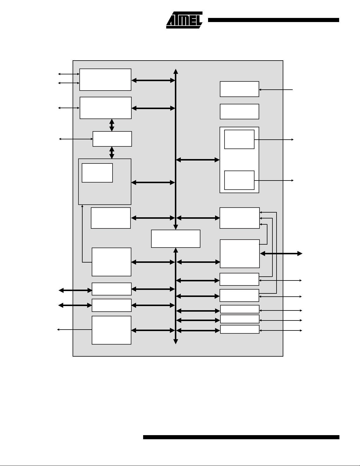
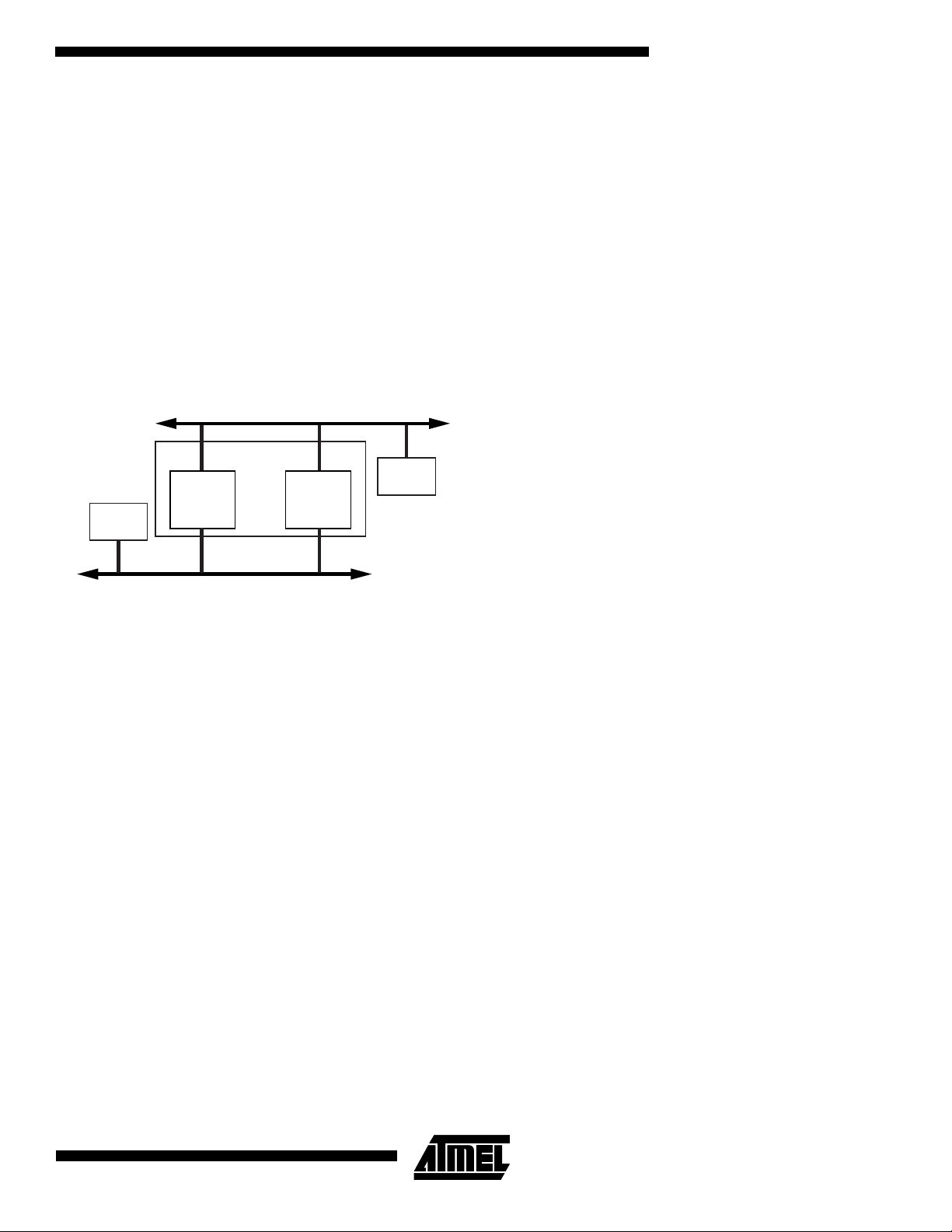
Figure 2. AT75C220 Block Diagram
Dual Ethernet
10/100 Mbps
MAC Interface
OakDSPCore
DSP Subsystem
ASB
Reset
Clocks
JTAG
Embedded
ICE
ARM7TDMI Core
Boot ROM
IRQ
Controller
PIO A
PIO B
Watchdog
Timer
SDRAM
Controller
External Bus
Interface
SRAM
Controller
Peripheral Data
Controller
AMBA Bridge
SPI
USART A
USART B
Timer/Counter 0
Timer/Counter 1
Timer/Counter 2
APB
6
AT75C220
Page 7
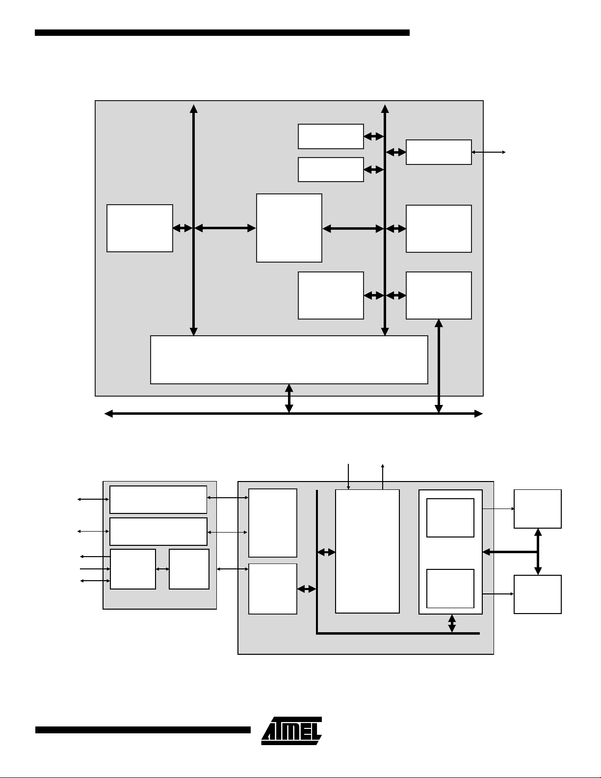
Figure 3. DSP Subsystem Block Diagram
Oak Program Bus Oak Data Bus
AT75C220
2K x 16 X-RAM
Codec Interface
2K x 16 Y-RAM
24K x 16
Program RAM
OakDSPCore
Emulation
Bus Interface Unit
DSP Subsystem
ASB
Figure 4. Application Example – Standalone Ethernet Telephone
Network
PC
Speaker
Microphone
Handset
Ethernet
10/100 Mbps PHY
Ethernet
10/100 Mbps PHY
Speaker
Phone
Interface
Analog Front End
Voice
Codec
Dual-port
Ethernet
10/100 Mbps
MAC
Interface
Voice
Processing
DSP Subsystem
On-chip
Module
Keyboard Screen
Protocol
ARM7TDMI Core
VolP
Stack
16K x 16
General-
purpose RAM
256 x 16
Dual-port
Mailbox
SDRAM
Controller
External Bus
Interface
SRAM
Controller
SDRAM
Flash
AT75C220
7
Page 8

Architectural Overview
The AT75C220 integrates an embedded ARM7TDMI processor. External SDRAM and SRAM/Flash interfaces are
provided so that processor code and data may be stored
off-chip.
The AT75C220 architecture consists of two main buses,
the Advanced System Bus (ASB) and the Advanced
Peripheral Bus (APB).
The ASB is designed for maximum performance. It interfaces the processor with the on-chip DSP subsystem and
the external memories and devices by the means of the
external bus interface (EBI).
The APB is designed for access to on-chip peripherals and
is optimized for low power consumption. The AMBA bridge
provides an interface between the ASB and APB.
The AT75C220 uses a multi-layer AMBA bus:
• It integrates two independent AMBA ASB buses. The two
buses are connected by a bridge that is not visible to the
other devices on the bus.
• The primary bus (ARM bus) is the main processor bus to
which most peripherals are connected.
• The secondary bus (MAC bus) is used exclusively for
Ethernet traffic.
The ARM7TDMI, USART DMA and ASB-ASB bridge
devices are masters on the ARM ASB bus, the MAC DMA
and ASB-ASB Bridge are masters on the MAC ASB bus
and the Flash/SRAM and SDRAM interfaces are ASB
slaves. For more details on bus arbitration, see “Arbitration
Using Multi-layer AMBA” on page 31.
All the peripherals are accessed by means of the APB bus.
An on-chip peripheral data controller (PDC) transfers data
between the on-chip USARTs and the memories without
processor intervention. Most importantly, the PDC removes
the processor input-handling overhead and significantly
reduces the number of clocks required for data transfer. It
can transfer up to 64K contiguous bytes without reprogramming the starting address. As a result, the performance of
the microcontroller is increased and power consumption
reduced.
The AT75C220 peripherals are designed to be programmed with a minimum number of instructions. Each
peripheral has 16K bytes of address space allocated in the
upper part of the address space. The peripheral register set
is composed of control, mode, data, status and interrupt
registers.
To maximize the efficiency of bit manipulation, frequentlywritten registers are mapped into three memory locations.
The first address is used to set the individual register bits,
the second resets the bit and the third address reads the
value stored in the register. A bit can be set or reset by writing a one to the corresponding position at the appropriate
address. Writing a zero has no effect. Individual bits can
thus be modified without having to use costly read-modifywrite and complex bit-manipulation instructions and without
having to store-disable-restore the interrupt state.
All of the external signals of the on-chip peripherals are
under the control of the parallel I/O controllers. The PIO
controllers can be programmed to insert an input filter on
each pin or generate an interrupt on a signal change. After
reset, the user must carefully program the PIO controllers
in order to define which peripherals are connected with offchip logic.
The ARM7TDMI processor operates in little-endian mode
in the AT75C220. The processor's internal architecture and
the ARM and Thumb instruction sets are described in the
ARM7TDMI datasheet, literature number 0673. The memory map and the on-chip peripherals are described in this
datasheet.
Peripheral Data Controller
The AT75C220 has a four-channel peripheral data controller (PDC) dedicated to the two on-chip USARTs. One PDC
channel is connected to the receiving channel and one to
the transmitting channel of each USART.
The user interface of a PDC channel is integrated in the
memory space of each USART channel. It contains a 32-bit
address pointer register and a 16-bit count register. When
the programmed number of bytes is transferred, an end-oftransfer interrupt is generated by the corresponding
USART. For more details on PDC operation and programming, see the section describing the USART on page 74 .
8
AT75C220
Page 9

Memory Map
AT75C220
The memory map is divided into regions of 256 megabytes.
The top memory region (0xF000_0000) is reserved and
subdivided for internal memory blocks or peripherals within
the AT75C220. The device can define up to six other active
external memory regions by means of the static memory
controller and SDRAM memory controller. See Table 2.
The memory map is divided between the two ASB buses.
All regions except the 16 megabytes between
0xFB00_0000 and 0xFBFF_FFFF are located on the ARM
ASB bus. Accesses to locations between 0xFB00_0000
and 0xFBFF_FFFF are routed to the MAC ASB bus.
The memory map assumes default values on reset. External memory regions can be reprogrammed to other base
addresses. For details, see “SMC: Static Memory Controller” on page 16 and “SDMC: SDRAM Controller” on page
24. Note that the internal memory regions have fixed locations that cannot be reprogrammed.
There are no hardware locks to prevent incorrect programming of the regions. Programming two or more regions to
have the same base address results in undefined behavior.
The ARM reset vector with address 0x00000000 is mapped
to internal ROM or external memory depending on the signal pin NDSRA/BOOTN. After booting, the ROM region can
be disabled and some external memory such as SDRAM or
Flash can be mapped to the bottom of the memory map by
programming SMC_CS0 or DMC_MR0.
Table 2. AT75C220 Memory Map
Default Base Address Region Type Normal Mode Boot Mode
0xFF000000 Internal APB Bridge
0xFE000000 Internal Reserved
0xFD000000 Internal Oak A Program RAM
(24K x 16 bits)
0xFC000000 Frame Buffer (16K x 16 bits)
0xFB000000 Internal Reserved (MAC ASB Bus)
0xFA000000 Internal Oak A DPMB (256 x 16 bits)
0xF9000000 Internal Boot ROM (1 KB)
0x50000000 External SDMC_CS1
0x40000000 External SDMC_CS0
0x30000000 External SMC_CS3
0x20000000 External SMC_CS2
0x10000000 External SMC_CS1
0x00000000 External/Internal SMC_CS0 Boot ROM
0x000003FF
0x00000000
9
Page 10

Peripheral Memory Map
The register maps for each peripheral are described in the corresponding section of this datasheet. The peripheral memory
map has 16K bytes reserved for each peripheral.
Table 3. AT75C220 Peripheral Memory Map
Base Address (Normal Mode) Peripheral Description
0xFF000000 MODE AT75C220 Mode Controller
0xFF004000 SMC Static Memory Controller
0xFF008000 SDMC SDRAM Controller
0xFF00C000 PIOA Programmable I/O
0xFF010000 PIO B Keypad PIO
0xFF014000 TC Timer/Counter Channels
0xFF018000 USARTA USART
0xFF01C000 USARTB USART
0xFF020000 SPI Serial Peripheral Interface
0xFF024000 Reserved
0xFF028000 WDT Watchdog Timer
0xFF030000 AIC Interrupt Controller
0xFF034000 MACA MAC Ethernet
0xFF038000 MACB MAC Ethernet
0xFFFFF000 AIC (alias) Interrupt Controller
Initialization
Reset initializes the user interface registers to their default
states as defined in the peripheral sections of this
datasheet and forces the ARM7TDMI to perform the next
instruction fetch from address zero. Except for the program
counter, the ARM core registers do not have defined reset
states. When reset is active, the inputs of the AT75C220
must be held at valid logic levels.
There are three ways in which the AT75C220 can enter
reset:
1. Hardware reset. Caused by asserting the RESET
pin, e.g., at power-up.
2. Watchdog timer reset. The WD timer can be pro-
grammed so that if timed out, a pulse is generated
that forces a chip reset.
3. Software reset. There are two software resets which
are asserted by writing to bits [11:10] of the SIAP
mode register. SIAP_MD[11] forces a software reset
with RM set low and SIAP_MD[10] forces a reset
with RM set high.
Reset Pin
The reset pin should be asserted for a minimum of 10 clock
cycles. However, if external DRAM is fitted, then reset
should be applied for the time interval specified by the
SDRAM datasheet, typically 200 µs. The OakDSPCores
are only released from reset by the ARM program control.
When reset is released, the pin NDSRA/BOOTN is sampled to determine if the ARM should boot from internal
ROM or from external memory connected to NCS0. The
details of this boot operation are described in the section
“Boot Mode” on page 11.
Processor Synchronization
The ARM and the OakDSPCore processors have their own
PLLs and at power-on each processor has its own indeterminate lock period. To guarantee proper synchronization of
inter-processor communication through the mailboxes, a
specific reset sequence should be followed.
Once the ARM core is out of reset, it should set and clear
the reset line of the OakDSPCore three times. This guarantees message synchronization between the ARM and the
OakDSPCore.
10
AT75C220
Page 11
Clocking
AT75C220
The AT75C220 mode register controls clock generation.
Oscillator and PLL
The AT75C220 uses an external 16 MHz crystal (XCLK)
and an on-chip PLL to generate the internal clocks. The
PLL generates a 240 MHz clock that is divided down to produce the ARM clock and Oak clock.
Oak System Clock
The Oak subsystem runs at 60MHz.
Other Clocks
The codec interfaces run from 800 kHz that is seperate
from the Oak clock.
The USARTs and timers operate from divided ARM clocks.
ARM System Clock
The ARM subsystem runs at 40 MHz.
Table 4. Clock Source and Frequency
Source Frequency Comment
Crystal 16 MHz External crystal
PLL Output 240 MHz Crystal multiplied by 15
ARM Clock 40 MHz PLL divided by 6
Oak Clock 60 MHz PLL divided by 4
Figure 5. AT75C220 Clocking
16 MHz
XTAL
XTALIN
.
.
15
.
.
6
40 MHz
ARM Core
Clock
10 pF
10 pF
1 MΩ
XTALOUT
Oscillator
16 MHz
PLL
XREF 240F
100 Ω
10 nF
Boot Mode
The AT75C220 has an integrated 1-Kbyte ROM to support
the boot software. When the device is released from reset,
the ARM starts fetching from address 0x00000000. If the
RM flag in the SIAP-E mode register (SIAP_MD on page
12) is low, the internal boot ROM is mapped to the bottom
1K byte of the memory map. If RM is high, the bottom 16M
bytes of memory address will default to external memory
region 0.
If NDSRA/BOOTN is asserted on reset, the internal boot
ROM program is executed. The boot program reads data
from USART A and writes it to the Oak Program RAM (in
the ARM memory map whereas the Oak is in reset). The
downloaded software can then configure the various con-
240 MHz
.
.
4
60 MHz
Phase
Generator
40 MHz
DSP Subsystem
Clock
trol registers in the AT75C220 and its peripherals so as to
perform external memory accesses. This allows the Flash
to be written.
The boot ROM code:
• sets CTS active
• waits for approximately three seconds for the start of a
Flash download sequence from the USART.
If the special header is not received, the AT75C220 boots
normally, i.e., from external memory at 0x00000000.
If the special header is received, the boot ROM enters the
code download process.
11
Page 12

AT75C220 Mode Controller
The ARM configures the mode of the AT75C220 by means
of the SIAP-E mode controller.
The SIAP-E mode controller is a memory-mapped peripheral that sits on the APB bus.
Register Map
Base Address: 0xFF000000
Table 5. AT75C220 Register Map
Register Address Register Name Description Access Reset Value
0x0 SIAP_MD SIAP-E Mode Register Read/write 0x00B0340
0x4 SIAP_ID SIAP-E ID Register Read-only 0x0000220
0x8 SIAP_RST SIAP-E Reset Status
Register
0xC SIAP_CLKF SIAP-E Clock Status
Register
Note: 1. If the PKG flag is set, the reset value is 0x00010220 since the AT75C220 is bonded in large bond-out mode.
Read/write 0x0000001
Read-only 0x0000001
SIAP-E Mode Register
Register Name: SIAP_MD
Access: Read/write
Reset Value: 0x00B0342
31 30 29 28 27 26 25 24
–– JCIDBG OUTDIV INDIV
(1)
23 22 21 20 19 18 17 16
ICP IPOLTST
15 14 13 12 11 10 9 8
– CRA – DBA SW2 SW1 LPCS
76543210
SA LP ––IA – RA RM
• RM: Remap
On reset being released this flag is set to the value of NDSRA/BOOTN. When RM is active low the Boot ROM is
mapped to location 0x00000000. Subsequently, this flag can be set high by software so that the ROM mapping is disabled and another memory controller region (e.g. FLASH) is mapped to location 0x00000000.
• RA: OAKA Reset
This flag resets to active low so that the OAKA is held in reset. The OAKA is be released from reset by asserting this
flag high.
• IA: Inhibit OAKA Clock
This flag resets to active low so that the OAKA clock is enabled. The OAKA clock is be inhibited by asserting this flag
high.
• LP: Low Power Mode
On reset this field is high. When written high the PLL is disabled and the ARM and OAK cores and logic are clocked at
the low power clock frequency. Note, in this mode the ARM and OAK are clocked at the same frequency determined by
the LPCS field. When LP is written low the PLL is enabled and once it has locked the clock is switched over to the normal operating frequency.
12
AT75C220
Page 13

AT75C220
• SA: Slow ARM Mode
On reset this field is low. In normal operating mode, if bit SA is set. The ARM clock is 34Mhz (i.e. the PLL value is
divided by 7). IF SA is not set the ARM clock is 40MHz (i..e the PLL divisor is 6). SA can be switched during low power
mode but should not be changed when LP is low.
• LPCS: Low Power Clock Select
This field is used to select a slower clock frequency for the ARM system clock as per the table below.
Oscillator Clock
LPCS
00 1 8 MHz
0 1 16 1 MHz
1 0 64 250 kHz
1 1 512 32 kHz
Divisor
ARM and Oak
System Clock
• SW1: Software Reset 1
Writing a 1 to this bit forces the SIAP into reset with RM set to 0.
• SW2: Software Reset 2
Writing a 1 to this bit forces the SIAP into reset with RM set to 1.
• DBA: OAKA Debug Mode
This flag resets low. To enter OAKA debug mode (specific pins are multiplexed out on functional pins), this bit should
be set.
• CRA: CODECA Reset
This flag resets to active low so that the CODECA is held in reset. The CODECA is released from reset by asserting
this flag high.
• IPOLTST: PLL Bias Adjustment
This can be used to tune the PLL if the bias current is not correct after manufacture.
Bias Factor 15 IPOLTST–()4⁄=
• ICP: PLL Charge Pump Current
This can be used to tune the PLL if it does not function with the default current of 2.5 µA.
IICP
( 1 )+ 2.5µA×=
• INDIV
Input frequency range of PLL.
INDIV PLL Input Frequency Range
0 0 5 kHz to 40 MHz
0 1 40 MHz to 80 MHz
1 0 80 MHz to 160 MHz
1 1 160 MHz to 250 MHz
13
Page 14
• OUTDIV
Output frequency range of PLL.
OUTDIV PLL Output Frequency Range
0 0 40 MHz to 250 MHz
0 1 20 MHz to 40 MHz
1 0 10 MHz to 20 MHz
1 1 5 MHz to 10 MHz
• JCIDBG
This field controls the mode of the JCI. The Oak subsystem has its own JTAG port. This port is used to communicate
serially with the Oak OCEM module.
SIAP-E ID Register
Register Name: SIAP_ID
Access: Read-only
Reset Value: 0x00000220 in small bond-out mode
0x0001220 in large bond-out mode
31 30 29 28 27 26 25 24
––––––––
23 22 21 20 19 18 17 16
–––––––PKG
15 14 13 12 11 10 9 8
76543210
IDENT
IDENT
• IDENT: Identifier
This field indicates the device identifier 0x0220.
• PKG: Package
This bit reflects the state of the data bus width signal DBW and indicates the SIAP package size.
14
AT75C220
Page 15
AT75C220
SIAP-E Reset Status Register
Register Name: SIAP_RST
Access: Read/write
Reset Value: 0x00000001
31 30 29 28 27 26 25 24
––––––––
23 22 21 20 19 18 17 16
––––––––
15 14 13 12 11 10 9 8
––––––––
76543210
–––––RST RST RST
• RST[2:0]: Reset
These bits indicate the cause of the last reset.
RST Reset Event
0 0 1 Hardware
0 1 0 Watchdog Timer
100 Software
SIAP-E Clock Status Register
Register Name: SIAP_CLKF
Access: Read-only
Reset Value: 0x00000001
31 30 29 28 27 26 25 24
––––––––
23 22 21 20 19 18 17 16
––––––––
15 14 13 12 11 10 9 8
––––––––
76543210
–––––––CLK
• CLK: Clock Status
This bit indicates which clock is in use by the system. When set, the low power clock is in use. When cleared, the PLL
is locked and the high power clock is in use. This can be used by software to determine when the power mode has
changed after the LP bit has been written.
15
Page 16

External Bus Interface
The external bus interface (EBI) generates the signals
which control access to external memories or peripheral
devices.
SMC: Static Memory Controller
The static memory controller (SMC) is used by the
AT75C220 to access external static memory devices.
Static memory devices include external Flash, SRAM or
peripherals.
The SMC provides a glueless memory interface to external
memory using the common address and data bus and
some dedicated control signals. The SMC is highly programmable and has up to 24 bits of address bus, a 32- or
16-bit data bus and up to four chip select lines. The SMC
supports different access protocols allowing single clockcycle accesses. The SMC is programmed as an internal
peripheral that has a standard APB bus interface and a set
of memory-mapped registers. The SMC shares the external address and data buses with the DMC and any external
bus master.
Table 6. Signal Interface
FPDRAM Description Type Notes
External Memory Mapping
The memory map associates the internal 32-bit address
space with the external 24-bit address bus. The memory
map is defined by programming the base address and
page size of the external memories. Note that A[2:23] is
only significant for 32-bit memory and A[1:23] for 16-bit
memory.
If the physical memory-mapped device is smaller than the
programmed page size, it wraps around and appears to be
repeated within the page. The SMC correctly handles any
valid access to the memory device within the page.
In the event of an access request to an address outside
any programmed page, an abort signal is generated by the
internal decoder. Two types of abort are possible: instruction prefetch abort and data abort. The corresponding
exception vector addresses are 0x0000000C and
0x00000010. It is up to the system programmer to program
the exception handling routine used in case of an abort.
If the AT75C220 is in internal boot mode, any chip select
configured with a base address of zero will be disabled as
the internal ROM is mapped to address zero.
A[23:0] Address bus Output
D[31:0] Data bus I/O
NCE[3:0] Active low chip enables Output
NWE[3:0] Active low byte select/write strobe signals Output
NWR Active low write strobe signals Output
NSOE Active low read enable signal Output
NWAIT Active low wait signal Input
Data Bus Width
A data bus width of 32 or 16 bits can be selected for each
chip select. This option is controlled by the DBW field in the
Chip Select Register (SMC_CSR) of the corresponding
chip select.
The AT75C220 always boots up with a data bus width of 16
bits set in SMC_CSR0.
Byte-write or Byte-select Mode
Each chip select with a 32-/16-bit data bus operates with
one or two different types of write mode:
1. Byte-write mode supports four (32-bit bus) or two
2. Byte-select mode selects the appropriate byte(s)
This option is controlled by the BAT field in SMC_CSR for
the corresponding chip select.
Byte-write access can be used to connect four 8-bit devices
as a 32-bit memory page or two 8-bit devices as a 16-bit
memory page.
D[15:0] used when data bus width is 16
NCE[3] can be configured for LCD interface mode
(16-bit bus) byte writes and a single read signal.
using four (32-bit bus) or two (16-bit bus) byte-select
lines and separate read and write signals.
16
AT75C220
Page 17

AT75C220
For a 32-bit bus:
• The signal NWE0 is used as the write enable signal for
byte 0.
• The signal NWE1 is used as the write enable signal for
byte 1.
• The signal NWE2 is used as the write enable signal for
byte 2.
• The signal NWE3 is used as the write enable signal for
byte 3.
• The signal NSOE enables memory reads to all memory
blocks.
For a 16-bit bus:
• The signal NWE0 is used as the write enable signal for
byte 0.
• The signal NWE1 is used as the write enable signal for
byte 1.
• The signal NSOE enables memory reads to all memory
blocks.
Byte-select mode can be used to connect one 32-bit device
or two 16-bit devices in a 32-bit memory page or one 16-bit
device in a 16-bit memory page.
For a 32-bit bus:
• The signal NWE0 is used to select byte 0 for read and
write operations.
• The signal NWE1 is used to select byte 1 for read and
write operations.
• The signal NWE2 is used to select byte 2 for read and
write operations.
• The signal NWE3 is used to select byte 3 for read and
write operations.
• The signal NWR is used as the write enable signal for
the memory block.
• The signal NSOE enables memory reads to the memory
block.
For a 16-bit bus:
• The signal NWE0 is used to select byte 0 for read and
write operations.
• The signal NWE1 is used to select byte 1 for read and
write operations.
• The signal NWR is used as the write enable signal for
the memory block.
• The signal NSOE enables memory reads to the memory
block.
During boot, the number of external devices (number of
active chip selects) and their configurations must be programmed as required. The chip select addresses that are
programmed take effect immediately. Wait states also take
effect immediately when they are programmed to optimize
boot program execution.
Read Protocols
The SMC provides two alternative protocols for external
memory read access: standard and early read. The difference between the two protocols lies in the timing of the
NSOE (read cycle) waveform.
The protocol is selected by the DRP field in the Memory
Control Register (SMC_MCR) and is valid for all memory
devices. Standard read protocol is the default protocol after
reset.
• Standard Read Protocol
Standard read protocol implements a read cycle in which
NSOE and the write strobes are similar. Both are active
during the second half of the clock cycle. The first half of
the clock cycle allows time to ensure completion of the previous access, as well as the output of address and NCE
before the read cycle begins.
During a standard read protocol external memory access,
NCE is set low and ADDR is valid at the beginning of the
access, whereas NSOE goes low only in the second half of
the master clock cycle to avoid bus conflict. The write
strobes are the same in both protocols. The write strobes
always go low in the second half of the master clock cycle.
• Early Read Protocol
Early read protocol provides more time for a read access
from the memory by asserting NSOE at the beginning of
the clock cycle. In the case of successive read cycles in the
same memory, NSOE remains active continuously. Since a
read cycle normally limits the speed of operation of the
external memory system, early read protocol allows a
faster clock frequency to be used. However, an extra wait
state is required in some cases to avoid contention on the
external bus.
In early read protocol, an early read wait state is automatically inserted when an external write cycle is followed by a
read cycle to allow time for the write cycle to end before the
subsequent read cycle begins. This wait state is generated
in addition to any other programmed wait states (i.e., data
float wait). No wait state is added when a read cycle is followed by a write cycle, between consecutive accesses of
the same type or between external and internal memory
accesses. Early read wait states affect the external bus
only. They do not affect internal bus timing.
Write Protocol
During a write cycle, the data becomes valid after the falling edge of the write strobe signal and remains valid after
the rising edge of the write strobe. The external write strobe
waveform on the appropriate write strobe pin is used to
control the output data timing to guarantee this operation.
Thus, it is necessary to avoid excessive loading of the write
strobe pins, which could delay the write signal too long and
cause a contention with a subsequent read cycle in standard protocol. In early read protocol, the data can remain
17
Page 18

valid longer than in standard read protocol due to the additional wait cycle that follows a write access.
Wait States
The SMC can automatically insert wait states. The different
types of wait states are:
• standard wait states
• data float wait states
• external wait states
• chip select change wait states
• early read wait states (see “Read Protocols” on page 17
for details)
• standard wait states
Each chip select can be programmed to insert one or more
wait states during an access on the corresponding device.
This is done by setting the WSE field in the corresponding
SMC_CSR. The number of cycles to insert is programmed
in the NWS field in the same register. The correspondence
between the number of standard wait states programmed
and the number of cycles during which the write strobe
pulse is held low is found in Table 7. For each additional
wait state programmed, an additional cycle is added.
Table 7. Correspondence Wait States/Number of Cycles
Wait States Cycles
01/2
SMC_CSR register for the corresponding chip select. The
value (0 - 7 clock cycles) indicates the number of data float
waits to be inserted and represents the time allowed for the
data output to go high impedance after the memory is disabled.
The SMC keeps track of the programmed external data
float time even when it makes internal accesses to ensure
that the external memory system is not accessed while it is
still busy.
Internal memory accesses and consecutive accesses to
the same external memory do not have added data float
wait states.
When data float wait states are being used, the SMC prevents the DMC or external master from accessing the
external data bus.
• External Wait
The NWAIT input can be used to add wait states at any
time NWAIT is active low and is detected on the rising edge
of the clock. If NWAIT is low at the rising edge of the clock,
the SMC adds a wait state and does not change the output
signals.
• Chip Select Change Wait States
A chip select wait state is automatically inserted when consecutive accesses are made to two different external memories (if no wait states have already been inserted). If any
wait states have already been inserted (e.g., data float
wait), then none are added.
11
• Data Float Wait State
Some memory devices are slow to release the external
bus. For such devices it is necessary to add wait states
(data float waits) after a read access before starting a write
access or a read access to a different external memory.
The Data Float Output Time (TDF) for each external memory device is programmed in the TDF field of the
LCD Interface Mode
NCE3 can be configured for use with an external LCD controller by setting the LCD bit in the SMC_CSR3 register.
Additionally, WSE must be set and NWS programmed with
a value of one or more.
In LCD mode, NCE3 is shortened by one-half clock cycle at
the leading and trailing edges, providing positive address
setup and hold. For read cycles, the data is latched in the
SMC as NCE3 is raised at the end of the access.
18
AT75C220
Page 19
AT75C220
SMC Register Map
The SMC is programmed using the registers listed in the
Table 8. The memory control register (SMC_MCR) is used
to program the number of active chip selects and data read
protocol. Four chip select registers (SMC_CSR0 to
SMC_CSR3) are used to program the parameters for the
Table 8. SMC Register Map
Offset Register Name Description Access Reset Value
0x00
SMC_CSR0
Chip Select Register
individual external memories. Each SMC_CSR must be
programmed with a different base address, even for
unused chip selects. The AT75C220 resets such that
SMC_CSR0 is configured as having a 16-bit data bus.
Read/write 0x0000203D
0x04
0x08
0x0C
0x10
0x14
0x18
0x1C
0x20
0x24
SMC_CSR1
SMC_CSR2
SMC_CSR3
–
–
–
–
–
SMC_MCR
Chip Select Register
Chip Select Register
Chip Select Register
Reserved
Reserved
Reserved
Reserved
Reserved
Memory Control Register
Read/write 0x10000000
Read/write 0x20000000
Read/write 0x30000000
––
––
––
––
––
Read/ write 0
SMC Chip Select Register
Register Name:SMC_CSR0..SMC_CSR3
Access: Read/write
Reset Value:
31 30 29 28 27 26 25 24
BA
23 22 21 20 19 18 17 16
BA –––LCD
15 14 13 12 11 10 9 8
––CSEN BAT TDF PAGES
76543210
PAGES MWS WSE NWS DBW
• DBW: Data Bus Width
DBW Data Bus Width
00Reserved
0 1 16-bit external bus
1 0 32-bit external bus
11Reserved
19
Page 20

• NWS: Number of Wait States
This field is valid only if WSE is set.
Table 9. NWS, WSE Values
NWS WSE Wait States
XX X 0 0
0001 1
0011 2
0101 3
0111 4
1001 5
1011 6
1101 7
1111 8
• WSE: Wait State Enable
• MWS: Multiply Wait States
See Table 9, where
WS NWS 1+()81+×=
• PAGES: Page Size
PAGES Page Size
0 0 1M byte BA[31 - 20]
0 1 4M bytes BA[31 - 22]
1 0 16M bytes BA[31 - 24]
11 Reserved –
• TDF: Data Float Output Time
TDF Cycles after Transfer
00 0 0
00 1 1
01 0 2
01 1 3
10 0 4
10 1 5
11 0 6
11 1 7
Base
Address
• BAT: Byte Access Mode
0 = Byte Write Mode
1 = Byte Select Mode
20
AT75C220
Page 21

AT75C220
• CSEN: Chip Select Enable
Active high.
• LCD: LCD Mode Enable
Active high. SMC_CSR3 only.
• BA: Base Address
This field contains the high-order bits of the base address. If the page size is larger than 1M byte, then the unused bits
of the base address are ignored by the SMC decoder.
SMC Memory Control Register
Register Name:SMC_MCR
31 30 29 28 27 26 25 24
––––––––
23 22 21 20 19 18 17 16
––––––––
15 14 13 12 11 10 9 8
––––––––
76543210
–––DRP ––––
• DRP: Data Read Protocol
0 = Standard Read Mode
1 = Early Read Mode
21
Page 22
Switching Waveforms
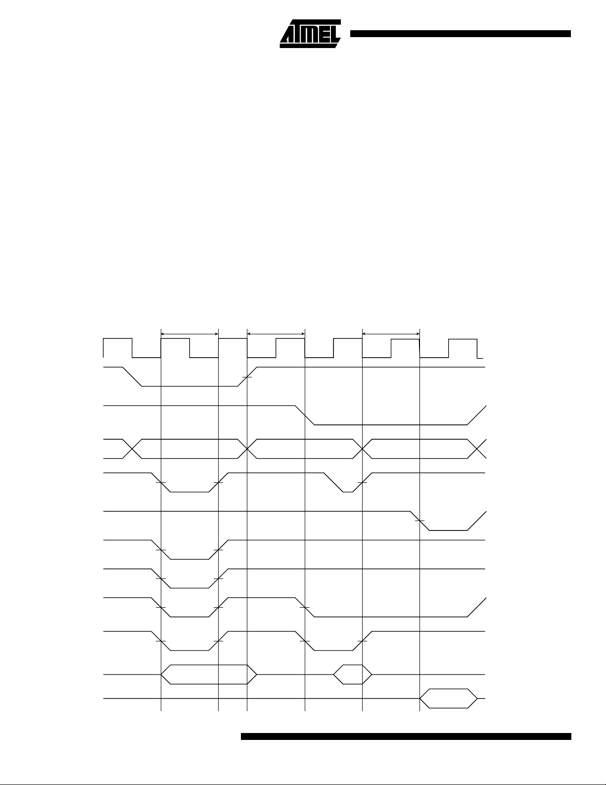
Figure 6 shows a write to memory 0 followed by a write and
a read to memory 1. SMC_CSR0 is programmed for one
wait state with BAT = 0 and DFT = 0. SMC_CSR1 is programmed for zero wait states with BAT = 1 and DFT = 0.
SMC_MCR is programmed for early reads from all
memories.
The write to memory 0 is a word access and therefore all
four NWE strobes are active. As BAT = 0, they are configured as write strobes and have the same timing as NWR.
As the access employs a single wait state, the write strobe
pulse is one clock cycle long.
There is a chip select change wait state between the memory 0 write and the memory 1 write. The new address is
output at the end of the memory 0 access, but the strobes
are delayed for one clock cycle.
The write to memory 1 is a half-word access to an odd halfword address and, therefore, NWE2 and NWE3 are active.
Figure 6. Write to Memory 0, Write and Read to Memory 1
Internal Wait State Chip Select Wait State Early Read Wait State
BCLK
As BAT = 1, they are configured as byte select signals and
have the same timing as NCE. As the access has no internal wait states, the write strobe pulse is one- half clock
cycle long. Data and address are driven until the write
strobe rising edge is sensed at the SIAP pin to guarantee
positive hold times.
There is an early read wait state between memory 1 write
and memory 1 read to provide time for the AT75C220 to
disable the output data before the memory is read. If the
read was normal mode, i.e., not early, the NSOE strobe
would not fall until the rising edge of BCLK and no wait
state would be inserted. If the write and early read were to
different memories, then the early read wait state is not
required as a chip select wait state will be implemented.
The read from memory 1 is a byte access to an address
with a byte offset of 2 and therefore only NWE2 is active.
NCE0
NCE1
NWR
NSOE
NWE0
NWE1
NWE2
NWE3
A
22
D (SIAP)
D (MEM)
AT75C220
Page 23
AT75C220
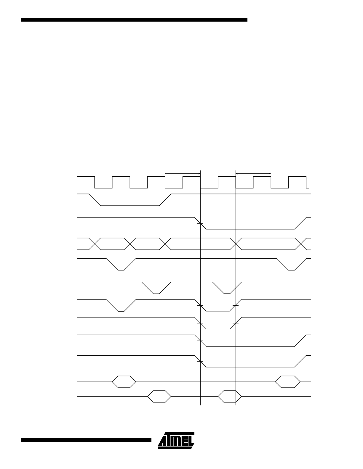
Figure 7 shows a write and a read to memory 0 followed by
a read and a write to memory 1. SMC_CSR0 is programmed for zero wait states with BAT = 0 and DFT = 0.
SMC_CSR1 is programmed for zero wait states with BAT =
1 and DFT = 1. SMC_MCR is programmed for normal
reads from all memories
The write to memory 0 is a byte access and, therefore, only
one NWE strobe is active. As BAT = 0, they are configured
as write strobes and have the same timing as NWR.
The memory 0 read immediately follows the write as early
reads are not configured and an early read wait state is not
required. As early reads are not configured, the read strobe
pulse is one-half clock cycle long.
There is a chip select change wait state between the memory 0 write and the memory 1 read. The new address is
output at the end of the memory 0 access but the strobes
are delayed for one clock cycle.
The write to memory 1 is a half-word access to an odd halfword address and, therefore, NWE2 and NWE3 are active.
As BAT = 1, they are configured as byte select signals and
have the same timing as NCE.
As DFT = 1 for memory 1, a wait state is implemented
between the read and write to provide time for the memory
to stop driving the data bus. DFT wait states are only implemented at the end of read accesses.
The read from memory 1 is a byte access to an address
with a byte offset of 2 and, therefore, only NWE2 is active.
Figure 7. Write and Read to Memory 0, Read and Write to Memory 1
Chip Select
Wait State
BCLK
NCE0
Data Float
Wait State
NCE1
NWR
NSOE
NWE0
NWE1
NWE2
NWE3
D (SIAP)
A
D (MEM)
23
Page 24

SDMC: SDRAM Controller
The AT75C220 integrates an SDRAM controller (SDMC).
The ARM accesses external SDRAM by means of the
SDRAM memory controller.
The SDMC shares the same address and data pins as the
static memory controller but has separate control signals.
The SDMC interface is a memory-mapped APB slave.
For very low frequency selection in low power mode, the
SDRAM should be refreshed frequently.
Table 10. External Memory Interface
Signal Name Type Description
DCLK Output SDRAM Clock
A[21:0] Output Memory address (Shared with SMC)
D[15:0] Input Memory data input (Shared with SMC)
DQM[1:0] Output SDRAM byte masks
CS0 Output SDRAM chip select, active low
CS1 Output SDRAM chip select, active high
Main features of the SDMC are:
• External memory mapping
• Up to 4 chip select lines
• 32- or 16-bit data bus
• Byte write or byte select lines
• Two different read protocols
• Programmable wait state generation
• External wait request
• Programmable data float time
• Programmable burst mode
WE Output SDRAM write enable, active low
RAS Output Row Address Select, active low
CAS Output Column Address Select, active low
The signals RAS, CAS, WE, A[21:0], and D[15:0] have
functions similar to those of a conventional DRAM.
DCLK is the free-running, normally continuous clock to
which all other signals are synchronized; CKE is an enable
signal that gates the other control inputs. Note that CKE is
not bonded out since it is always active high.
APB Interface
The SDMC interface is a memory-mapped APB slave.
ASB Interface
The SDMC is also an ASB slave and has a reserved memory region in the ASB memory map.
Read and Write Bursts
The SDMC has been modified so read accesses are performed in bursts of four for accesses to 32-bit memory or
bursts of eight for 32-bit access to 16-bit memory. Read
accesses are performed as shown in Figure 8, Figure 9
and Figure 10. Note that read bursts are terminated if a
non-sequential access is detected. However, pipelined
commands from the SDRAM may be still be executed but
the resultant read data is ignored.
Three separate read accesses are shown in Figure 8, Figure 9 and Figure 10. In Figure 8, the data from all four
reads is used, in Figure 9 the data from the last two reads
is discarded. Figure 10 shows a single non-sequential
access to a new row.
24
AT75C220
Page 25
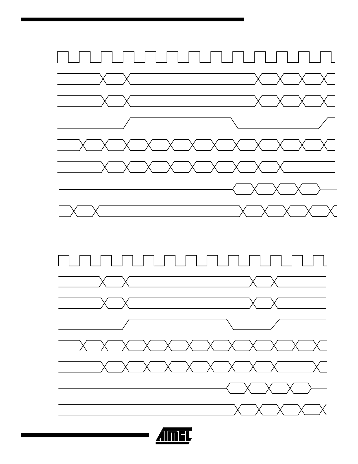
Figure 8. Read with Burst Length of 4 and CAS Latency of 2
P
BCLK
AT75C220
BA
BTRAN
BWAIT
SDRAM CMD
addr
sdmc_data
BD
NOP PRE NOP ACT NOP READ READ READ READ NOP NOP NO
A0 A2 A3A1
NSEQ SEQ SEQ SEQ NSEQ
BANK ROW COL0 COL1 COL2 COL3
Figure 9. Read with Burst Length of 2 and CAS Latency of 2
D0 D1 D2 D3
D0 D1 D2 D3
BCLK
BA
BTRAN
BWAIT
SDRAM CMD
Addr
sdmc_data
BD
A0 A2 A3A1
NSEQ SEQ SEQ SEQ
NOP PRE NOP ACT NOP READ READ READ READ NOP NOP PRE
BANK ROW COL0 COL1 COL2 COL3
D0 D1 D2 D3
D0 D1 x x
BANK
25
Page 26
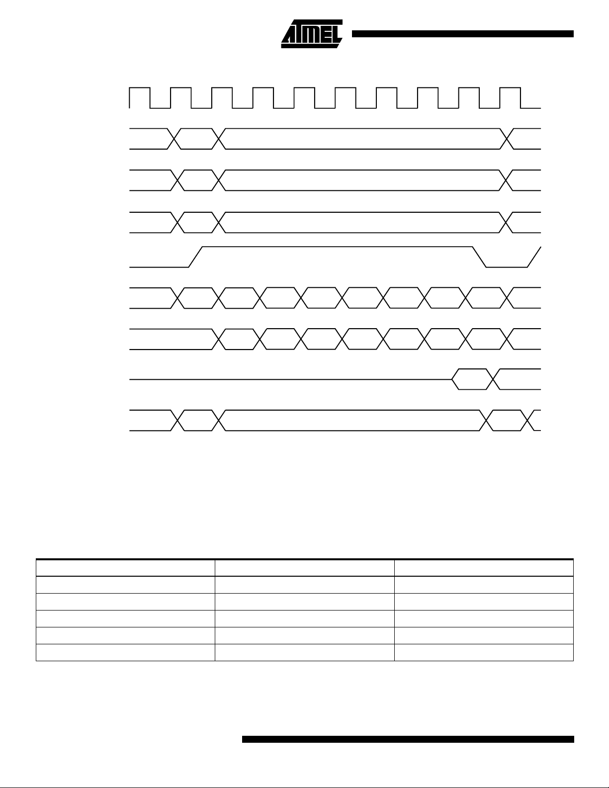
Figure 10. Read Showing a Single Access for a Non-sequential Read to a New Row
BCLK
BA
BTRAN
hburst_h
BWAIT
SDRAM CMD
Addr
sdmc_data
BD
A0 A1
NSEQ NSEQ
INCR INCR
NOP PRE NOP ACT NOP READ NOP NOP
BANK ROW COL0 COL1
NOP
D0
D0
Writes can burst continuously until any of the following conditions are achieved:
1. The following access is a read.
2. The following access is to a new row.
3. The following access is non-sequential.
When any of these conditions occur, the write burst is broken and SDMC goes inactive.
Table 11. SDRAM Refresh Rates
Clock Speed (MHz) Tick (us) Counter Needed
40 0.25 62.5
81.2512.5
1 10 1.5625
0.025 400 0.0390625
0.0032 3125 0.005
SDRAM Refresh
Table 11 shows the counter values needed for a refresh
rate of 15.625 µs in the SDMC. As can be seen, at clock
speeds of 1 MHz and below it is unfeasible to maintain data
integrity in the SDRAM. Note that in low power modes it is
not a requirement to maintain data in the SDRAM.
26
AT75C220
Page 27
AT75C220
SDMC Register Map
Base Address: 0xFF008000
Table 12. SDMC Register Map
Offset Register Name Description Access Reset Value
0x0000 SDRAM_MODE Mode Register Read/write 0x00000000
0x0004 SDRAM_TIMER Timer Register Read/write 0x00000000
0x0008 SDRAM_CFG Configuration Register Read/write 0x00000000
0x000C SDRAM_16BIT Selects 16-/32-bit modes Read/write 0x00000001
0x0010 SDRAM_CS0_ADDR Base address for CS0 Read/write 0x00000040
0x0014 SDRAM_CS1_ADDR Base address for CS1 Read/write 0x00000050
SDRAM_MODE Register
Register Name: SDRAM_MODE
Access Type: Read/write
Reset Value: 0x0
31 30 29 28 27 26 25 24
––––––––
23 22 21 20 19 18 17 16
––––––––
15 14 13 12 11 10 9 8
–––––––MODE
76543210
MODE ––––––
• MODE
MODE Description
000 Normal mode. Any access to the SDRAM will be decoded normally.
001 The NOP command is issued to the SDRAM when the host accesses the SDRAM memory area, regardless of the
cycle.
010 The all banks precharge command is issued to the SDRAM when the host accesses the SDRAM memory area,
regardless of the cycle.
011 The load mode register command is issued to the SDRAM when the host accesses the SDRAM memory area,
regardless of the cycle. The address offset with respect to the SDRAM memory base address is used to program the
mode register. For example, when this mode is activated, an access to the “SDRAM_BASE + offset” generates a load
mode register command with the value offset written to the mode register of the SDRAM.
100 A refresh command is issued to the SDRAM. An all banks precharge command must precede.
others Reserved
27
Page 28
SDRAM_TIMER Register
Register Name: SDRAM_TIMER
Access Type: Read/write
Reset Value: 0x0
31 30 29 28 27 26 25 24
––––––––
23 22 21 20 19 18 17 16
––––––––
15 14 13 12 11 10 9 8
–––– CNT
76543210
CNT
• CNT
This 12-bit field is loaded into a timer which generates the refresh pulse. Each time the refresh pulse is generated, a
refresh burst is initiated. The length of this refresh burst (number of rows refreshed) can be adjusted at compile time by
modifying the value RFSH_LEN. The refresh commands will begin when the timer is loaded for the first time. The value
to be loaded depends on the clock frequency used in the SDMC configuration module, the refresh rate of the SDRAM
and the refresh burst length where 15.6 microseconds is a typical value for a burst of length one.
SDRAM_CFG Register
Register Name: SDRAM_CFG
Access Type: Read/write
Reset Value: 0x0
31 30 29 28 27 26 25 24
––––– TRAS
23 22 21 20 19 18 17 16
15 14 13 12 11 10 9 8
TRP TRC TWR
76543210
TWR CAS NB NR NC
TRCD TRP
• NC
Sets the number of column bits. Default is eight column bits.
NC Column Bits
00 8
01 9
10 10
11 11
28
AT75C220
Page 29
AT75C220
• NR
Sets the number of row bits. Default is 11 row bits.
NR Row Bits
00 11
01 12
10 13
11 Reserved
• NB
Sets the number of banks. Default is two banks.
NB Number of Banks
02
14
• CAS
Sets the CAS latency. The SDMC has been modified so that it only supports a CAS latency of two. Writing to this register will have no effect.
• TWR
Sets the value of TWR expressed in number of cycles. Default is two cycles.
• TRC
Sets the value of TRC expressed in number of cycles. Default is eight cycles.
• TRP
Sets the value of TRP expressed in number of cycles. Default is three cycles.
• TRCD
Sets the value of TRCD expressed in number of cycles. Default is three cycles.
• TRAS
Sets the value of TRAS expressed in number of cycles. Default is five cycles.
SDRAM_16bit Register
Register Name: SDRAM_16BIT
Access Type: Read/write
Reset Value: 0x1
31 30 29 28 27 26 25 24
––––––––
23 22 21 20 19 18 17 16
––––––––
15 14 13 12 11 10 9 8
––––––––
76543210
–––––––16BIT
• 16BIT
This bit is used to set the width of the external memory. If this field is set, the address is assumed to be 16 bits wide. If
not set, the memory bus is assumed to be 32 bits wide.
29
Page 30

SDRAM_CS0_ADDR Register
Register Name: SDRAM_CS0_ADDR
Access Type: Read/write
Reset Value: 0x40
31 30 29 28 27 26 25 24
––––––––
23 22 21 20 19 18 17 16
––––––––
15 14 13 12 11 10 9 8
–––––––CS0_ADDR
76543210
CS0_ADDR
• CS0_ADDR
This bit is used to set the eight most significant bits of the address of CS0.
SDRAM_CS1_ADDR Register
Register Name: SDRAM_CS1_ADDR
Access Type: Read/write
Reset Value: 0x50
31 30 29 28 27 26 25 24
––––––––
23 22 21 20 19 18 17 16
––––––––
15 14 13 12 11 10 9 8
–––––––CS1_ADDR
76543210
• CS1_ADDR
This bit is used to set the eight most significant bits of the address of CS1.
CS1_ADDR
30
AT75C220
Page 31
Arbitration Using Multi-layer AMBA
AT75C220
The AT75C220 has two separate ASB (multi-layer AMBA)
buses that can be decoupled during most normal operations. The ability to couple the two ASB buses is provided
to allow the ARM to receive and transmit Ethernet frames
via the two Ethernet MACs.
The ARM bus is the main processor bus to which most
peripherals are connected.
The MAC bus is used exclusively for Ethernet traffic.
An ASB-ASB bridge that is transparent to the other devices
on the bus connects the two ASB buses. Figure 11 shows
the connection between the two buses.
Figure 11. ASB - ASB Bridge
ASB (ARM)
MAC
Arbiter
ASB - ASB Bridge
Slave
Master
Master
Slave
ASB (MAC)
ARM
Arbiter
The ASB-ASB bridge consists of two channels: the first is a
master on the MAC bus and a slave on the ARM bus. The
second channel is a master on the ARM bus and a slave on
the MAC bus.
The ARM7TDMI is the default master and always requests
the bus. It is always granted the bus in absence of a
request from another master.
The MAC ASB has two priority levels, the two MACs share
low priority access and the bridge has high priority. The
MACs do not burst more than four words per access and
release the bus request between accesses so the MACs
can share a priority level with a simple round-robin arbitration scheme.
The ARM is likely to be the only master accessing the MAC
bus via the bridge and should not perform more than a couple of cycles before releasing the MAC bus. Care should be
taken to prevent other masters on the ARM bus holding the
MAC bus for more than a few cycles. Otherwise, the MACs
drop frames due to FIFO overflow or underflow.
Coupled Bus Operation
When a master on one bus accesses a slave on the other
bus, the following operations occur:
• The master arbitrates for the local ASB bus if it does not
already have access to the bus.
• When the local bus arbiter grants the master the local
bus, the master initiates a cycle with an address
corresponding to a slave on the remote bus.
• The bridge is selected as the slave on the local bus and
responds by inserting wait cycles. The bridge also
requests the remote bus from the remote bus arbiter.
• When the bridge is granted the remote bus, the two ASB
buses are coupled and the transfer completes.
ASB-ASB Bridge Timing
The AMBA ASB performs pipelined arbitration. The bridge
can only request the bus when the address of the slave is
available. For this reason, the bridge must insert a wait
cycle during the arbitration cycle on the remote bus
because it cannot request the bus early. Figure 12 shows a
write cycle from a master on the ARM bus to a slave on the
MAC bus. The slave does not add wait states. All cycles
operate in the same way as the write cycle until the buses
are coupled when the operation becomes slavedependent.
Deadlock
Deadlock is avoided by forcing the ARM processor to
release the bus if both the ARM and one of the MACs
request the bridge at the same time. The bridge responds
to the ARM with a signal to force the ARM to retry the operation later. The MAC can complete its access and release
the bus in the normal way.
Deadlock can still occur if a master that does not support
retract attempts to access the MAC bus at the same time
as one of the MACs is requesting the ARM bus. This situation is avoided if only the ARM is used to access the MAC
bus.
31
Page 32

Figure 12. ASB-to-ASB Bridge Write Timing
BCLK
ARM Bus Signals
BTRAN
BA/BWRITE
DSEL
BWAIT
BD
MAC Bus Signals
BREQ
BGNT
BTRAN
BA/BWRITE
DSEL
BWAIT
BD
32
AT75C220
Page 33

Ethernet MAC
AT75C220
The AT75C220 integrates two identical Ethernet MACs,
known as MAC A and MAC B.
The Ethernet MAC is described more fully in the IEEE standard 802.3. It is a programmable device on the APB bus by
means of 56 configuration and status registers. The Ethernet MAC is an ASB master.
The main features of the Ethernet MAC are:
• Compatibility with IEEE standard 802.3
• 10 and 100 Mbit/s operation
• Full-and half-duplex operation
• MII interface to the physical layer
• Register interface to address, status and control
registers
Table 13. External Interface
Signal Name Description Type
COL Collision detect from the PHY Input
CRS Carrier sense from the PHY Input
TXER Transmit error signal to the PHY. Asserted if the DMA block fails to fetch data
from memory during frame transmission.
TXD[3:0] Transmit data to the PHY Output
• DMA interface
• Interrupt generation to signal receive and transmit
completion
• 28-byte transmit and 28-byte receive FIFOs
• Automatic pad and CRC generation on transmitted
frames
• Address checking logic to recognize four 48-bit
addresses
• Supports promiscuous mode where all valid frames are
copied to memory
• Supports physical layer management through MDIO
interface
Output
TXEN Transmit enable to the PHY Output
TXCLK Transmit clock from the PHY Input
RXD[3:0] Receive data from the PHY Input
RXER Receive error signal from the PHY Input
RXCLK Receive clock from the PHY Input
RXDV Receive data valid signal from the PHY Input
MDC Management data clock Output
MDIO Management data I/O Input/Output
DMA Operation
Frame data is transferred to and from the Ethernet MAC via
the DMA interface. All transfers are 32-bit words and may
be single accesses or bursts of two, three or four words.
Burst accesses do not cross 16-byte boundaries.
The DMA controller performs four types of operations on
the ASB bus. In order of priority, they are receive buffer
manager write, receive buffer manager read, transmit data
DMA read and receive data DMA write.
Transmitter Mode
Transmit frame data needs to be stored in contiguous
memory locations and need not be word-aligned.
The transmit address register is written with the address of
the first byte to be transmitted. Transmit is initiated by writ-
ing the number of bytes to transfer (length) to the transmit
control register. The transmit channel then reads data from
memory 32 bits at a time and places them in the transmit
FIFO.
The transmit block starts frame transmission once three
words have been loaded into the FIFO.
The transmit address register must be written before the
transmit control register. While a frame is being transmitted, it is possible to set up one other frame for transmission
by writing new values to the transmit address and control
registers. Reading the transmit address register returns the
address of the buffer currently being accessed by the transmit FIFO. Reading the transmit control register returns the
total number of bytes to be transmitted. The buffer not
queued bit in the transmit status register indicates whether
33
Page 34

another buffer can be safely queued. An interrupt is generated whenever this bit is set.
Frame assembly starts by adding preamble and the start
frame delimiter. Data is taken from the transmit FIFO wordby-word. If necessary, padding is added to make the frame
length 60 bytes. The CRC is calculated as a 32-bit polynomial. This is inverted and appended to the end of the frame,
making the frame length a minimum of 64 bytes. The CRC
is not appended if the NCRC bit is set in the transmit control register.
In full duplex mode frames are transmitted immediately.
Back-to-back frames are transmitted at least 96 bit times
apart to guarantee the interframe gap.
In half-duplex mode the transmitter checks carrier sense. If
asserted, it waits for it to de-assert and then starts transmission after the interframe gap of 96 bit times.
If the collision signal is asserted during transmission, the
transmitter will transmit a jam sequence of 32 bits taken
from the data register and then retry transmission after the
backoff time has elapsed. An error is indicated and any further attempts aborted if 16 attempts cause collisions.
If transmit DMA underruns, bad CRC is automatically
appended using the same mechanism as jam insertion.
Underrun also causes TXER to be asserted.
Receiver Mode
When a packet is received, it is checked for valid preamble,
CRC, alignment, length and address. If all these criteria are
met, the packet is stored successfully in a receive buffer. If
at the end of reception the CRC is bad, then the received
buffer is recovered.
Each received frame including CRC is written to a single
receive buffer.
Receive buffers are word-aligned and are capable of containing 1518 bytes of data (the maximum length of an
Ethernet frame).
The start location for each received frame is stored in
memory in a list of receive buffer descriptors at a location
pointed to by the receive buffer queue pointer register.
Each entry in the list consists of two words. The first word is
the address of the received buffer; the second is the
receive status. Table 14 defines an entry in the received
buffer descriptor list.
To receive frames, the buffer queue must be initialized by
writing an appropriate address to bits [31:2] in the first word
of each list entry. Bit zero must be written with zero. After a
frame is received, bit zero becomes set and the second
word indicates what caused the frame to be copied to
memory.
The start location of the received buffer descriptor list
should be written to the received buffer queue pointer register before receive is enabled (by setting the receive
enable bit in the network control register). As soon as the
received block starts writing received frame data to the
receive FIFO, the received buffer manager reads the first
receive buffer location pointed to by the received buffer
queue pointer register. If the filter block is active, the frame
should be copied to memory; the receive data DMA operation starts writing data into the receive buffer. If an error
occurs, the buffer is recovered. If the frame is received
without error, the queue entry is updated. The buffer
pointer is rewritten to memory with its low-order bit set to
indicate successful frame reception and a used buffer. The
next word is written with the length of the frame and how
the destination address was recognized.
The next receive buffer location is then read from the following word or, if the current buffer pointer had its wrap bit
set, the beginning of the table. The maximum number of
buffer pointers before a wrap bit is seen is 1024. If a wrap
bit is not seen by then, a wrap bit is assumed in that entry.
The received buffer queue pointer register must be written
with zero in its lower-order bit positions to enable the wrap
function to work correctly.
If bit zero is set when the receive buffer manager reads the
location of the receive buffer, then the buffer has already
been used and cannot be used again until software has
processed the frame and cleared bit zero. In this case, the
DMA block will set the buffer’s unavailable bit in the
received status register and trigger an interrupt. The frame
will be discarded and the queue entry will be reread on
reception of the next frame to see if the buffer is now available. Each discarded frame increments a statistics register
that is cleared on being read.
When there is network congestion, it is possible for the
MAC to be programmed to apply backpressure. This is
when half-duplex mode collisions are forced on all received
frames by transmitting 64 bits of data (a default pattern).
Reading the received buffer queue register returns the
location of the queue entry currently being accessed. The
queue wraps around to the start after either 1024 entries
(i.e., 2048 words) or when the wrap bit is found to be set in
bit 1 of the first word of an entry.
34
AT75C220
Page 35

AT75C220
Table 14. Received Buffer Descriptor List
Bit Function
Word 0
31:2 Address of beginning of buffer
1 Wrap bit. If this bit is set, the counter that is ORed with the received buffer queue pointer register to give the
pointer to entries in this table will be cleared after the buffer is used.
0 Ownership bit. 1 indicates software owns the pointer, 0 indicates that the DMA owns the buffer. If this bit is not
zero when the entry is read by the receiver, the buffer’s unavailable bit is set in the received status register and
the receiver goes inactive.
Word 1
31 Global all ones broadcast address detected
30 Multicast hash match
29 Unicast hash match
28 External address (optional)
27 Unknown source address (reserved for future use)
26 Local address match (Specific address 4 match)
25 Local address match (Specific address 3 match)
24 Local address match (Specific address 2 match)
23 Local address match (Specific address 1 match)
22:11 Reserved written to 0.
10:0 Length of frame including FCS
Address Checking
Whether or not a frame is stored depends on what is
enabled in the network configuration register, the contents
of the specific address and hash registers and the frame's
destination address. In this implementation of the MAC the
frame’s source address is not checked.
A frame will not be copied to memory if the MAC is transmitting in half-duplex mode at the time a destination
address is received.
The hash register is 64 bits long and takes up two locations
in the memory map.
There are four 48-bit specific address registers, each taking up two memory locations. The first location contains the
first four bytes of the address; the second location contains
the last two bytes of the address stored in its least significant byte positions. The addresses stored can be specific,
group, local or universal.
Ethernet frames are transmitted a byte at a time, LSB first.
The first bit (i.e., the LSB of the first byte) of the destination
address is the group/individual bit and is set one for multicast addresses and zero for unicast. This bit corresponds
to bit 24 of the first word of the specific address register.
The MSB of the first byte of the destination address corresponds to bit 31 of the specific address register.
The specific address registers are compared to the destination address of received frames once they have been
activated. Addresses are deactivated at reset or when the
first byte [47:40] is written and activated or when the last
byte [7:0] is written. If a receive frame address matches an
active address, the local match signal is set and the store
frame pulse signal is sent to the DMA block via the HCLK
synchronization block.
A frame can also be copied if a unicast or multicast hash
match occurs, it has the broadcast address of all ones, or
the copy all frames bit in the network configuration register
is set.
The broadcast address of 0xFFFFFFFF is recognized if the
no broadcast bit in the network configuration register is
zero. This sets the broadcast match signal and triggers the
store frame signal.
The unicast hash enable and the multicast hash enable bits
in the network configuration register enable the reception of
35
Page 36

hash matched frames. So all multicast frames can be
received by setting all bits in the hash register.
The CRC algorithm reduces the destination address to a 6bit index into a 64-bit hash register. If the equivalent bit in
the register is set, the frame will be matched depending on
whether the frame is multicast or unicast and the appropriate match signals will be sent to the DMA block
If the copy all frames bit is set in the network configuration
register, the store frame pulse will always be sent to the
DMA block as soon as any destination address is received.
Register Map
Base Address MAC A: 0xFF034000
Base Address MAC B: 0xFF038000
Table 15. Ethernet MAC Register Map
Offset Register Name Description Access Reset Value
0x00 ETH_CTL Network Control Register Read/write 0x0
0x04 ETH_CFG Network Configuration Register Read/write 0x800
0x08 ETH_SR Network Status Register Read-only 0x4
0x0C ETH_TAR Transmit Address Register Read/write 0x0
0x10 ETH_TCR Transmit Control Register Read/write 0x0
0x14 ETH_TSR Transmit Status Register Read/write 0x18
0x18 ETH_RBQP Receive buffer queue pointer Read/write 0x0
0x1C – Reserved Read-only 0x0
0x20 ETH_RSR Receive Status Register Read/write 0x0
0x24 ETH_ISR Interrupt Status Register Read/write 0x0
0x28 ETH_IER Interrupt Enable Register Write-only –
0x2C ETH_IDR Interrupt Disable Register Write-only –
0x30 ETH_IMR Interrupt Mask Register Read-only 0xFFFF
0x34 ETH_MAN PHY Maintenance Register Read/write 0x0
Statistics Registers
0x40 ETH_FRA Frames transmitted OK Read/write 0x0
0x44 ETH_SCOL Single collision frames Read/write 0x0
0x48 ETH_MCOL Multiple collision frames Read/write 0x0
0x4C ETH_OK Frames received OK Read/write 0x0
0x50 ETH_SEQE Frame check sequence errors Read/write 0x0
0x54 ETH_ALE Alignment errors Read/write 0x0
0x58 ETH_DTE Deferred transmission frames Read/write 0x0
0x5C ETH_LCOL Late collisions Read/write 0x0
0x60 ETH_ECOL Excessive collisions Read/write 0x0
0x64 ETH_CSE Carrier sense errors Read/write 0x0
0x68 ETH_TUE Transmit underrun errors Read/write 0x0
0x6C ETH_CDE Code errors Read/write 0x0
0x70 ETH_ELR Excessive length errors Read/write 0x0
36
AT75C220
Page 37

AT75C220
Table 15. Ethernet MAC Register Map (Continued)
Offset Register Name Description Access Reset Value
0x74 ETH_RJB Receive jabbers Read/write 0x0
0x78 ETH_USF Undersize frames Read/write 0x0
0x7C ETH_SQEE SQE test errors Read/write 0x0
0x80 ETH_DRFC Discarded RX frames Read/write 0x0
Address Registers
0x90 ETH_HSH Hash Register [63:32] Read/write 0x0
0x94 ETH_HSL Hash Register [31:0] Read/write 0x0
0x98 ETH_SA1L Specific address 1, first 4 bytes Read/write 0x0
0x9C ETH_SA1H Specific address 1, last 2 bytes Read/write 0x0
0xA0 ETH_SA2L Specific address 2, first 4 bytes Read/write 0x0
0xA4 ETH_SA2H Specific address 2, last 2 bytes Read/write 0x0
0xA8 ETH_SA3L Specific address 3, first 4 bytes Read/write 0x0
0xAC ETH_SA3H Specific address 3, last 2 bytes Read/write 0x0
0xB0 ETH_SA4L Specific address 4, first 4 bytes Read/write 0x0
0xB4 ETH_SA4H Specific address 4, last 2 bytes Read/write 0x0
MAC Network Control Register
Register Name: ETH_CTL
Access Type: Read/write
Reset Value: 0x0
31 30 29 28 27 26 25 24
––––––––
23 22 21 20 19 18 17 16
––––––––
15 14 13 12 11 10 9 8
–––––––BP
76543210
WES ISR CSR MPE TE RE LBL LB
• LB
Loopback. Optional.
• LBL
Loopback local. Connects TXD to RXD, TXEN to RXDV, forces full duplex and drives RXCLK and TXCLK with HCLK
divided by 4.
• RE
Receive enable. When set, enables the Ethernet MAC to receive data.
• TE
Transmit enable. When set, enables the Ethernet transmitter to send data.
37
Page 38

• MPE
Management port enable. Set to one to enable the management port. When zero forces MDIO to high impedance
state.
• CSR
Clear statistics registers. This bit is write-only. Writing a one clears the statistics registers.
• ISR
Increment statistics registers. This bit is write-only. Writing a one increments all the statistics registers by one for test
purposes.
• WES
Write enable for statistics registers. Setting this bit to one makes the statistics registers writable for functional test
purposes.
• BP
Back pressure. If this field is set, then in half-duplex mode collisions are forced on all received frames by transmitting
64 bits of data (default pattern).
MAC Network Configuration Register
Register Name: ETH_CFG
Access Type: Read/write
Reset Value: 0x8
31 30 29 28 27 26 25 24
––––––––
23 22 21 20 19 18 17 16
––––––––
15 14 13 12 11 10 9 8
–––RTY CLK EAE BIG
76543210
UNI MTI NBC CAF – BR FD SPD
• SPD
Speed. Set to 1 to indicate 100Mbit/sec. operation, 0 for 10Mbit/sec. Has no other functional effect.
• FD
Full duplex. If set to 1, the transmit block ignores the state of collision and carrier sense and allows receive while
transmitting.
• BR
Bit rate. Optional.
• CAF
Copy all frames. When set to 1, all valid frames will be received.
• NBC
No broadcast. When set to 1, frames addressed to the broadcast address of all ones will not be received.
• MTI
Multicast hash enable, when set multicast frames will be received when six bits of the CRC of the destination address
point to a bit that is set in the hash register.
• UNI
Unicast hash enable. When set, unicast frames will be received when six bits of the CRC of the destination address
point to a bit that is set in the hash register.
38
AT75C220
Page 39

AT75C220
• BIG
Receive 1522 bytes. When set, the MAC will receive up to 1522 bytes. Normally the MAC will receive frames up to
1518 bytes in length.
• EAE
External address match enable. Optional.
• CLK
The system clock (HCLK) is divided down to generate MDC (the clock for the MDIO). For conformance with IEEE 802.3
MDC must not exceed 2.5 MHz. At reset this field is set to 10 so that HCLK is divided by 32.
CLK MDC
00 HCLK divided by 8
01 HCLK divided by 16
10 HCLK divided by 32
11 HCLK divided by 64
• RTY
Retry test. When set, the time between frames will always be one time slot. For test purposes only. Must be cleared for
normal operation.
MAC Network Status Register
Register Name: ETH_SR
Access Type: Read-only
Reset Value: 0x4
31 30 29 28 27 26 25 24
––––––––
23 22 21 20 19 18 17 16
––––––––
15 14 13 12 11 10 9 8
––––––––
76543210
–––––IDLE MDIO LINK
• LINK
The status of the LINK pin. Optional.
• MDIO
Returns status of the MDIO pin.
• IDLE
The PHY management logic is idle (i.e., has completed).
39
Page 40

MAC Transmit Address Register
Register Name: ETH_TAR
Access Type: Read/write
Reset Value: 0x0
31 30 29 28 27 26 25 24
ADDRESS
23 22 21 20 19 18 17 16
ADDRESS
15 14 13 12 11 10 9 8
ADDRESS
76543210
ADDRESS
• ADDRESS
Transmit address register. Written with the address of the frame to be transmitted, read as the base address of the
buffer being accessed by the transmit FIFO. Note if the two least significant bits are not zero, transmit will start at the
byte indicated.
MAC Transmit Control Register
Register Name: ETH_TCR
Access Type: Read/write
Reset Value: 0x0
31 30 29 28 27 26 25 24
––––––––
23 22 21 20 19 18 17 16
––––––––
15 14 13 12 11 10 9 8
NCRC –––– LEN
76543210
LEN
• LEN
Transmit frame length. This register is written to the number of bytes to be transmitted excluding the four CRC bytes
unless the no CRC bit is asserted. Writing these bits to any non-zero value will initiate transmit. If the value is greater
than 1514 (1518 if no CRC is being generated), an oversize frame will be transmitted. This field is buffered so that a
new frame can be queued while the previous frame is still being transmitted. Must always be written in address-thenlength order. Reads as the total number of bytes to be transmitted (i.e., this value does not change as the frame is
transmitted.) Frame transmission will not start until two 32-bit words have been loaded into the transmit FIFO. The
length must be great enough to ensure two words are loaded.
• NCRC
No CRC. If this bit is set, it is assumed that the CRC is included in the length being written in the low-order bits and the
MAC will not append CRC to the transmitted frame. If the buffer is not at least 64 bytes long, a short frame will be sent.
This field is buffered so that a new frame can be queued while the previous frame is still being transmitted. Reads as
the value of the frame currently being transmitted.
40
AT75C220
Page 41

AT75C220
MAC Transmit Status Register
Register Name: ETH_TSR
Access Type: Read/write
Reset Value: 0x18
31 30 29 28 27 26 25 24
––––––––
23 22 21 20 19 18 17 16
––––––––
15 14 13 12 11 10 9 8
––––––––
76543210
– UND COMP BNQ IDLE RLE COL OVR
• OVR
Ethernet transmit buffer overrun. Software wrote to the address register or length register when bit 4 was not set.
Cleared by writing a one to this bit.
• COL
Collision occurred. Set by the assertion of collision. Cleared by writing a one to this bit.
• RLE
Retry limit exceeded. Cleared by writing a one to this bit.
• IDLE
Transmitter Idle. Asserted when the transmitter has no frame to transmit. Will be cleared when a length is written to
transmit frame length portion of the Transmit Control register. This bit is read-only.
• BNQ
Ethernet transmit buffer not queued. Software may write a new buffer address and length to the transmit DMA controller. Cleared by having one frame ready to transmit and another in the process of being transmitted. This bit is readonly.
• COMP
Transmit complete. Set when a frame has been transmitted. Cleared by writing a one to this bit.
• UND
Transmit underrun. Set when transmit DMA was not able to read data from memory in time. If this happens, the transmitter will force bad CRC. Cleared by writing a one to this bit.
41
Page 42

MAC Receive Buffer Queue Pointer
Register Name: ETH_RBQP
Access Type: Read/write
Reset Value: 0x0
31 30 29 28 27 26 25 24
ADDRESS
23 22 21 20 19 18 17 16
ADDRESS
15 14 13 12 11 10 9 8
ADDRESS
76543210
ADDRESS
• ADDRESS
Receive buffer queue pointer. Written with the address of the start of the receive queue, reads as a pointer to the current buffer being used. The receive buffer is forced to word alignment.
MAC Receive Status Register
Register Name: ETH_RSR
Access Type: Read/write
Reset Value: 0x0
31 30 29 28 27 26 25 24
––––––––
23 22 21 20 19 18 17 16
––––––––
15 14 13 12 11 10 9 8
––––––––
76543210
–––––OVR REC BNA
• BNA
Buffer not available. An attempt was made to get a new buffer and the pointer indicated that it was owned by the processor. The DMA will reread the pointer each time a new frame starts until a valid pointer is found. This bit will be set at
each attempt that fails even if it has not had a successful pointer read since it has been cleared. Cleared by writing a
one to this bit.
• REC
Frame received. One or more frames have been received and placed in memory. Cleared by writing a one to this bit.
• OVR
RX overrun. The DMA block was unable to store the receive frame to memory, either because the ASB bus was not
granted in time or because a not OK HRESP was returned. The buffer will be recovered if this happens. Cleared by
writing a one to this bit.
42
AT75C220
Page 43

AT75C220
MAC Interrupt Status Register
Register Name: ETH_ISR
Access Type: Read/write
Reset Value: 0x0
31 30 29 28 27 26 25 24
––––––––
23 22 21 20 19 18 17 16
––––––––
15 14 13 12 11 10 9 8
––––HRESP ROVR LINK TIDLE
76543210
TCOM TBRE RTRY TUND TOVR RBNA RCOM DONE
• DONE
Management done. The PHY maintenance register has completed its operation. Cleared on read.
• RCOM
Receive complete. A frame has been stored in memory. Cleared on read.
• RBNA
Receive buffer not available. Cleared on read.
• TOVR
Transmit buffer overrun. Software wrote to the address register or length register when bit 4 of the transmit status register was not set. Cleared on read.
• TUND
Transmit error. Ethernet transmit buffer underrun. The transmit DMA did not complete fetch frame data in time for it to
be transmitted. Cleared on read.
• TRLE
Transmit error. Retry limit exceeded. Cleared on read.
• TBRE
Transmit buffer register empty. Software may write a new buffer address and length to the transmit DMA controller.
Cleared by having one frame ready to transmit and another in the process of being transmitted. Cleared on read.
• TCOM
Transmit complete. Set when a frame has been transmitted. Cleared on read.
• LINK
Set when LINK pin changes value. Optional.
• TIDLE
Transmit idle. Set when all frames have been transmitted. Cleared on read.
• ROVR
RX overrun. Set when the RX overrun status bit is set. Cleared on read.
• HRESP
HRESP not OK. Set when the DMA block sees HRESP not OK. Cleared on read.
43
Page 44

MAC Interrupt Enable Register
Register Name: ETH_IER
Access Type: Write-only
Reset Value: –
31 30 29 28 27 26 25 24
––––––––
23 22 21 20 19 18 17 16
––––––––
15 14 13 12 11 10 9 8
––––HRESP ROVR LINK TIDLE
76543210
TCOM TBRE RTRY TUND TOVR RBNA RCOM DONE
• DONE
Enable management done interrupt.
• RCOM
Enable receive complete interrupt.
• RBNA
Enable receive buffer not available interrupt.
• TOVR
Enable Ethernet transmit buffer overrun interrupt
• TUND
Enable transmit buffer underrun interrupt
• RTRY
Enable retry limit exceeded interrupt.
• TBRE
Enable transmit buffer register empty interrupt.
• TCOM
Enable transmit complete interrupt.
• LINK
Enable LINK interrupt. Optional.
• TIDLE
Enable transmit idle interrupt.
• ROVR
Enable RX overrun interrupt.
• HRESP
Enable HRESP not OK interrupt.
44
AT75C220
Page 45

AT75C220
MAC Interrupt Disable Register
Register Name: ETH_IDR
Access Type: Write-only
Reset Value: –
31 30 29 28 27 26 25 24
––––––––
23 22 21 20 19 18 17 16
––––––––
15 14 13 12 11 10 9 8
––––HRESP ROVR LINK TIDLE
76543210
TCOM TBRE RTRY TUND TOVR RBNA RCOM DONE
• DONE
Disable management done interrupt.
• RCOM
Disable receive complete interrupt.
• RBNA
Disable receive buffer not available interrupt.
• TOVR
Disable Ethernet Transmit buffer overrun interrupt.
• TUND
Disable transmit buffer underrun interrupt.
• RTRY
Disable retry limit exceeded interrupt.
• TBRE
Disable transmit buffer register empty interrupt.
• TCOM
Disable transmit complete interrupt.
• LINK
Disable LINK interrupt. Optional.
• TIDLE
Disable transmit idle interrupt.
• ROVR
Disable Rx overrun interrupt.
• HRESP
Disable HRESP not OK interrupt.
45
Page 46

MAC Interrupt Mask Register
Register Name: ETH_IMR
Access Type: Read-only
Reset Value: 0xFFFF
31 30 29 28 27 26 25 24
––––––––
23 22 21 20 19 18 17 16
––––––––
15 14 13 12 11 10 9 8
––––HRESP ROVR LINK TIDLE
76543210
TCOM TBRE RTRY TUND TOVR RBNA RCOM DONE
• DONE
Management done interrupt masked.
• RCOM
Receive complete interrupt masked.
• RBNA
Receive buffer not available interrupt masked.
• TOVR
Ethernet Transmit buffer overrun interrupt masked
• TUND
Transmit buffer underrun interrupt masked
• RTRY
Retry limit exceeded interrupt masked.
• TBRE
Transmit buffer register empty interrupt masked.
• TCOM
Transmit complete interrupt masked.
• LINK
LINK interrupt masked.
• TIDLE
Transmit idle interrupt masked.
• ROVR
Receive overrun interrupt masked.
• HRESP
HRESP not OK interrupt masked.
46
AT75C220
Page 47

AT75C220
MAC PHY Maintenance Register
Register Name: ETH_MAN
Access Type: Read/write
Reset Value: 0x0
31 30 29 28 27 26 25 24
LOW HIGH RW PHYA
23 22 21 20 19 18 17 16
PHYA REGA CODE
15 14 13 12 11 10 9 8
DATA
76543210
DATA
Writing to this register starts the shift register that controls the serial connection to the PHY. On each shift cycle the MDIO
pin becomes equal to the MSB of the shift register and LSB of the shift register becomes equal to the value of the MDIO
pin. When the shifting is complete an interrupt is generated and the IDLE field is set in the Network Status register.
When read will give current shifted value.
• DATA
For a write operation this is written with the data to be written to the PHY. After a read operation this contains the data
read from the PHY.
• CODE
Must be written to 10. Will read as written.
• REGA
Register address. Specifies the register in the PHY to access.
• PHYA
PHY address. Normally will be 0.
• RW
Read/write Operation. 10 is read. 01 is write. Any other value is an invalid PHY management frame.
• HIGH
Must be written with 1 to make a valid PHY management frame.
• LOW
Must be written with 0 to make a valid PHY management frame.
47
Page 48

MAC Hash Address High
Register Name: ETH_HSH
Access Type: Read/write
Reset Value: 0x0
31 30 29 28 27 26 25 24
ADDR
23 22 21 20 19 18 17 16
ADDR
15 14 13 12 11 10 9 8
ADDR
76543210
ADDR
• ADDR
Hash Address bits 63 to 32.
MAC Hash Address Low
Register Name: ETH_HSL
Access Type: Read/write
Reset Value: 0x0
31 30 29 28 27 26 25 24
ADDR
23 22 21 20 19 18 17 16
ADDR
15 14 13 12 11 10 9 8
ADDR
76543210
ADDR
• ADDR
Hash Address bits 31 to 0.
48
AT75C220
Page 49

AT75C220
MAC Specific Address (1, 2, 3 and 4) High
Register Name: ETH_SA1H,...ETH_SA4H
Access Type: Read/write
Reset Value: 0x0
31 30 29 28 27 26 25 24
––––––––
23 22 21 20 19 18 17 16
––––––––
15 14 13 12 11 10 9 8
ADDR
76543210
ADDR
• ADDR
Unicast Addresses (1, 2, 3 and 4), Bits 47:32.
MAC Specific Address (1, 2, 3 and 4) Low
Register Name: ETH_SA1L,...ETH_SA4L
Access Type: Read/write
Reset Value: 0x0
31 30 29 28 27 26 25 24
ADDR
23 22 21 20 19 18 17 16
ADDR
15 14 13 12 11 10 9 8
ADDR
76543210
ADDR
• ADDR
Unicast Addresses (1, 2, 3 and 4), Bits 31:0.
49
Page 50

MAC Statistics Register Block
These registers reset to zero on a read and stick at all ones
when they count to their maximum value. They should be
read frequently enough to prevent loss of data.
Table 16. Statistics Register Block
Register Name Description
ETH_FRA Frames transmitted OK. A 24-bit register counting the number of frames successfully transmitted.
ETH_SCOL Single collision frames. A 16-bit register counting the number of frames experiencing a single collision
before being transmitted and experiencing no carrier loss nor underrun.
ETH_MCOL Multiple collision frames. A 16-bit register counting the number of frames experiencing between two and
fifteen collisions prior to being transmitted (62 - 1518 bytes, no carrier loss, no underrun).
ETH_OK Frames received OK. A 24-bit register counting the number of good frames received, i.e. address
recognized. A good frame is of length 64 to 1518 bytes and has no FCS, alignment or code errors.
ETH_SEQE Frame checks sequence errors. An 8-bit register counting address-recognized frames with an integral
number of bytes long and that have bad CRC and 64 to 1518 bytes long.
ETH_ALE Alignment errors. An 8-bit register counting frames that are:
- address recognized,
- not an integral number of bytes long
- have bad CRC when their length is truncated to an integral number of bytes
- between 64 and 1518 bytes in length.
ETH_DTE Deferred transmission frames. A 16-bit register counting the number of frames experiencing deferral due to
carrier sense active on their first attempt at transmission (no underrun or collision).
ETH_LCOL Late collisions. An 8-bit register counting the number of frames that experience a collision after the slot
time (512 bits) has expired. No carrier loss or underrun. A late collision is counted twice, i.e., both as a
collision and a late collision.
ETH_ECOL Excessive collisions. An 8-bit register counting the number of frames that failed to be transmitted because
they experienced 16 collisions. (64 - 1518 bytes, no carrier loss or underrun)
The statistics register block contains the registers found in
Table 16.
ETH_CSE Carrier sense errors. An 8-bit register counting the number of frames for which carrier sense was not
detected and maintained in half-duplex mode a slot time (512 bits) after the start of transmission (no
excessive collision).
ETH_TUE Transmit errors. An 8-bit register counting the number of frames not transmitted due to a transmit DMA
underrun. If this register is incremented, then no other register is incremented.
ETH_CDE Code errors. An 8-bit register counting the number of frames that are address recognized, had RXER
asserted during reception. If this counter is incremented, then no other counters are incremented.
ETH_ELR Excessive length frames. An 8-bit register counting the number of frames received exceeding 1518 bytes
in length but that do not have either a CRC error, an alignment error or a code error.
ETH_RJB Receive jabbers. An 8-bit register counting the number of frames received exceeding 1518 bytes in length
and having either a CRC error, an alignment error or a code error.
ETH_USF Undersize frames. An 8-bit register counting the number of frames received less than 64 bytes in length
but that do not have either a CRC error, an alignment error or a code error.
ETH_SQEE SQEE test errors. An 8-bit register counting the number of frames where COL was not asserted within a
slot time of TXEN being deasserted.
ETH_DRFC Discarded receive frames count. This 16-bit counter is incremented every time an address-recognized
frame is received but cannot be copied to memory because the receive buffer is available.
50
AT75C220
Page 51

AIC: Advanced Interrupt Controller
AT75C220
The AT75C220 integrates the Atmel advanced interrupt
controller (AIC). For details on this peripheral, refer to the
datasheet, literature number 1246.
The interrupt controller is connected to the fast interrupt
request (NFIQ) and the standard interrupt request (NIRQ)
inputs of the ARM7TDMI processor. The processor’s NFIQ
line can only be asserted by the external fast interrupt
request input (FIQ). The NIRQ line can be asserted by the
Figure 13. Advanced Interrupt Controller Block Diagram
FIQ Source
Advanced Peripheral
Bus (APB)
Internal Interrupt Sources
External Interrupt Sources
Memorization
Control
Logic
Memorization
interrupts generated by the on-chip peripherals and the two
external interrupt request lines, IRQ0 to IRQ1.
An 8-level priority encoder allows the user to define the priority between the different interrupt sources. Internal
sources are programmed to be level-sensitive or edge-triggered. External sources can be programmed to be positiveor negative-edge triggered or high- or low-level sensitive.
NFIQ
ARM7TDMI
Core
NIRQ
Prioritization
Controller
NFIQ
Manager
NIRQ
Manager
Table 17. Interrupt Sources
Interrupt Source Interrupt Name Interrupt Description
0 FIQ Fast Interrupt (LOWP)
1 WDT Watchdog Interrupt
2 SWI Software Interrupt
3 UARTA USART A Interrupt
4 TC0 Timer Channel 0 Interrupt
5 TC1 Timer Channel 1 Interrupt
6 TC2 Timer Channel 2 Interrupt
7 PIOA PIO A Interrupt
8 MACA MAC A Interrupt
9 SPI Serial Peripheral Interface
10 IRQ0 External Interrupt
11 IRQ1 External Interrupt
12 OAKA OAK Semaphore Interrupt
13 MACB MAC B Interrupt
51
Page 52

Table 17. Interrupt Sources (Continued)
Interrupt Source Interrupt Name Interrupt Description
14 UARTB USART B Interrupt
15 PIOB PIO B Interrupt
16 - 31 Reserved
Priority Controller
The NIRQ line is controlled by an 8-level priority encoder.
Each source has a programmable priority level of 7 to 0.
Level 7 is the highest priority and level 0 the lowest.
When the AIC receives more than one unmasked interrupt
at a time, the interrupt with the highest priority is serviced
first. If both interrupts have equal priority, the interrupt with
the lowest interrupt source number is serviced first.
The current priority level is defined as the priority level of
the current interrupt at the time the register AIC_IVR is
read (the interrupt which will be serviced). In the case when
a higher priority unmasked interrupt occurs while an interrupt already exists, there are two possible outcomes
depending on whether the AIC_IVR has been read.
1. If the NIRQ line has been asserted but the AIC_IVR
has not been read, then the processor will read the
new higher priority interrupt handler number in the
AIC_IVR register and the current interrupt level is
updated.
2. If the processor has already read the AIC_IVR, then
the NIRQ line is reasserted. When the processor
has authorized nested interrupts to occur and reads
the AIC_IVR again, it reads the new, higher priority
interrupt handler address. At the same time the current priority value is pushed onto a first-in last-out
stack and the current priority is updated to the
higher priority.
When the End of Interrupt Command Register
(AIC_EOICR) is written, the current interrupt level is
updated with the current interrupt level from the stack (if
any). Hence, at the end of a higher priority interrupt, the
AIC returns to the previous state corresponding to the preceding lower priority interrupt which had been interrupted.
Interrupt Handling
The interrupt handler must read the AIC_IVR as soon as
possible. This deasserts the NIRQ request to the processor
and clears the interrupt in case it is programmed to be
edge-triggered. This permits the AIC to assert the NIRQ
line again when a higher priority unmasked interrupt
occurs.
At the end of the interrupt service routine, the End of Interrupt Command Register (AIC_EOICR) must be written.
This allows pending interrupts to be serviced.
Interrupt Masking
Each interrupt source, including FIQ, can be enabled or
disabled using the command registers AIC_IECR and
AIC_IDCR. The interrupt mask can be read in the read only
register AIC_IMR. A disabled interrupt does not affect the
servicing of other interrupts.
Interrupt Clearing and Setting
All interrupt sources which are programmed to be edgetriggered (including FIQ) can be individually set or cleared
by respectively writing to the registers AIC_ISCR and
AIC_ICCR. This function of the interrupt controller is available for auto-test or software debug purposes.
Standard Interrupt Sequence
It is assumed that:
• The advanced interrupt controller has been
programmed, AIC_SVR registers are loaded with
corresponding interrupt service routine addresses and
interrupts are enabled.
When NIRQ is asserted and if the bit I of CPSR is 0, the
sequence is as follows:
1. The CPSR is stored in SPSR_irq, the current value
of the Program Counter is loaded in the IRQ link
register (R14_IRQ) and the Program Counter (R15)
is loaded with 0x18. In the following cycle during
fetch at address 0x1C, the ARM core adjusts
R14_IRQ, decrementing it by 4.
2. The ARM core enters IRQ mode if it is not already.
3. When the instruction at 0x18 is executed, the Pro-
gram Counter is loaded with the value read in the
AIC_IVR. Reading the AIC_IVR has the following
effects:
Sets the current interrupt to be the pending one with
the highest priority. The current level is the priority level
of the current interrupt.
De-assserts the nIRQ line on the processor (even if
vectoring is not used, AIC_IVR must be read in order to
de-assert nIRQ).
Automatically clears the interrupt if it has been programmed to be edge-triggered.
Pushes the current level on to the stack.
Returns the AIC_SVR corresponding to the current
interrupt.
52
AT75C220
Page 53

AT75C220
4. The previous step establishes a connection to the
corresponding ISR. This begins by saving the link
register (R14_IRQ) and the SPSR (SPSR_IRQ).
Note that the link register must be decrermented by
4 when it is saved if it is to be restored directly into
the Program Counter at the end of the interrupt.
5. Further interrupts can then be unmasked by clearing the I bit in the CPSR, allowing re-assertion of
the NIRQ to be taken into account by the core. This
can occur if an interrupt with a higher priority than
the current one occurs.
6. The interrupt handler then proceeds as required,
saving the registers which are used and restoring
them at the end. During this phase, an interrupt of
priority higher than the current level will restart the
sequence from step 1. Note that if the interrupt is
programmed to be level-sensitive, the source of the
interrupt must be cleared during this phase.
7. The I bit in the CPSR must be set in order to mask
interrupts before exiting to ensure that the interrupt
is completed in an orderly manner.
8. The service routine should then connect to the common exit routine.
9. The End Of Interrupt Command Register
(AIC_EOICR) must be written in order to indicate to
the AIC that the current interrupt is finished. This
causes the current level to be popped from the
stack, restoring the previous current level if one
exists. If another interrupt with lower or equal priority than the old current level is pending, the nIRQ
line is re-asserted but the interrupt sequence does
not immediately start because the I bit is set in the
core.
10. The SPSR (SPSR_IRQ) is restored. Finally, the
saved value of the Link Register is restored directly
into the PC. This has the effect of returning from the
interrupt to the step previously executed, of loading
the CPSR with the stored SPSR and of masking or
unmasking the interrupts depending on the state
saved in the SPSR (the previous state of the ARM
core).
Note: The I bit in the SPSR is significant. If it is set, it indicates
that the ARM core was just about to mask IRQ interrupts
when the mask instruction was interrupted. Hence, when
the SPSR is restored, the mask instruction is completed
(IRQ is masked).
Fast Interrupt
The external FIQ line is the only source which can raise a
fast interrupt request to the processor. Therefore it has no
priority controller. It can be programmed to be positive- or
negative-edge triggered or high- or low-level sensitive in
the AIC_SMR0 register.
The fast interrupt handler address can be stored in the
AIC_SVR0 register. The value written into this register is
available by reading the AIC_FVR register when an FIQ
interrupt is raised. By storing the following instruction at
address 0x0000001C, the processor will load the program
counter with the interrupt handler address stored in the
AIC_FVR register.
LDR PC, [PC, #-&F20]
Alternatively, the interrupt handler can be stored starting
from address 0x0000001C as described in the ARM7TDMI
datasheet.
Fast Interrupt Sequence
It is assumed that:
• The advanced interrupt controller has been
programmed, AIC_SVR[0] is loaded with the fast
interrupt service routine address and the fast interrupt is
enabled.
• Nested fast interrupts are not needed by the user.
When NFIQ is asserted, if the bit F of CPSR is 0, the
sequence is:
1. The CPSR is stored in SPSR_fiq, the current value
of the Program Counter is loaded in the FIQ link
register (R14_FIQ) and the Program Counter (R15)
is loaded with 0x1C. In the following cycle, during
fetch at address 0x20, the ARM core adjusts
R14_FIQ, decrementing it by 4.
2. The ARM core enters FIQ mode.
3. When the instruction loaded at address 0x1C is
executed, the Program Counter is loaded with the
value read in AIC_FVR. Reading the AIC_FVR has
the effect of clearing the fast interrupt (source 0
connected to the FIQ line) if it has been programmed to be edge-triggered. In this case only, it
de-asserts the nFIQ line on the processor.
4. The previous step establishes a connection to the
corresponding interrupt service routine. It is not
necessary to save the Link Register (R14_FIQ) and
the SPSR (SPSR_FIQ) if nested fast interrupts are
not needed.
5. The interrupt handler can then proceed as required.
It is not necessary to save registers R8 to R13
because FIQ mode has its own dedicated registers
and the user R8 to R13 are banked. The other registers, R0 to R7, must be saved before being used
and restored at the end (before the next step). Note
that if the fast interrupt is programmed to be levelsensitive, the source of the interrupt must be
53
Page 54

cleared during this phase in order to de-assert the
NFIQ line.
6. Finally, the Link Register (R14_FIQ) is restored into
the PC after decrementing it by 4 (e.g., with instruction SUB PC, LR, #4). This has the effect of
returning from the interrupt to the step previously
executed, of loading the CPSR with the SPSR and
of masking or unmasking the fast interrupt depending on the state saved in the SPSR.
Note: The F bit in the SPSR is significant. If it is set, it indicates
that the ARM core was just about to mask FIQ interrupts
when the mask instruction was interrupted. Hence, when
the SPSR is restored, the interrupted instruction is completed (FIQ is masked).
Software Interrupt
Any interrupt source of the AIC can be a software interrupt.
It must be programmed to be edge-triggered in order to set
or clear it by writing to the AIC_ISCR and AIC_ICCR. This
is totally independent of the SWI instruction of the
ARM7TDMI processor.
Spurious Interrupt
A spurious interrupt is a signal of very short duration on one
of the interrupt input lines. A spurious interrupt also arises
when an interrupt is triggered and masked in the same
cycle.
Spurious Interrupt Sequence
A spurious interrupt is handled by the following sequence
of actions.
1. When an interrupt is active, the AIC asserts the
nIRQ (or nFIQ) line and the ARM7TDMI enters IRQ
(or FIQ) mode. At this moment, if the interrupt
source disappears, the nIRQ (or nFIQ) line is deasserted but the ARM7TDMI continues with the
interrupt handler.
2. If the IRQ Vector Register (AIC_IVR) is read when
the nIRQ is not asserted, the AIC_IVR is read with
the contents of the Spurious Interrupt Vector
Register.
3. If the FIQ Vector Register (AIC_FVR) is read when
the nFIQ is not asserted, the AIC_FVR is read with
the contents of the Spurious Interrupt Vector
Register.
4. The Spurious ISR must write an End of Interrupt
command as a minimum, however, it is sufficient to
write to the End of Interrupt Command Register
(AIC_EOICR). Until the AIC_EOICR write is
received by the interrupt controller, the nIRQ (or
nFIQ) line is not re-asserted.
5. This causes the ARM7TDMI to jump into the Spurious Interrupt Routine.
6. During a spurious ISR, the AIC_ISR reads 0.
54
AT75C220
Page 55

AT75C220
AIC User Interface
Base Address: 0xFF030000
Table 18. AIC Memory Map
Offset Register Name Register Access Reset State
0x000
0x004
–
0x07C
0x080
0x084
–
0xFC0
0x100
0x104
0x108
0x10C
0x110
0x114
0x118
0x11C
0x120
0x124
0x128
0x12C
0x130 AIC_EOICR End-of-interrupt Command Register Write-only –
AIC_SMR0
AIC_SMR1
–
AIC_SMR31
AIC_SVR0
AIC_SVR1
–
AIC_SVR31
AIC_IVR
AIC_FVR
AIC_ISR
AIC_IPR
AIC_IMR
AIC_CISR
–
–
AIC_IECR
AIC_IDCR
AIC_ICCR
AIC_ISCR
Source Mode Register 0
Source Mode Register 1
–
Source Mode Register 31
Source Vector Register 0
Source Vector Register 1
–
Source Vector Register 31
IRQ Vector Register
FIQ Vector Register
Interrupt Status Register
Interrupt Pending Register
Interrupt Mask Register
Core Interrupt Status Register
Reserved
Reserved
Interrupt Enable Command Register
Interrupt Disable Command Register
Interrupt Clear Command Register
Interrupt Set Command Register
Read/write
Read/write
–
Read/write
Read/write
Read/write
–
Read/write
Read-only
Read-only
Read-only
Read-only
Read-only
Read-only
–
–
Write-only
Write-only
Write-only
Write-only
See Note 1
0
0
–
0
0
0
–
0
0
0
0
0
0
–
–
–
–
–
–
0x134 AIC_SPU Spurious Interrupt Vector Register Read/write 0
Note: 1. The reset value of this register depends on the level of the external IRQ lines. All other sources are cleared at reset.
AIC Source Mode Register
Register Name: AIC_SMR0...AIC_SMR31
Access Type:Read/write
Reset Value: 0
31 30 29 28 27 26 25 24
––––––––
23 22 21 20 19 18 17 16
––––––––
15 14 13 12 11 10 9 8
––––––––
76543210
– SRCTYPE –– PRIOR
• PRIOR: Priority Level
Programs the priority level for all sources except source 0 (FIQ).
The priority level can be between 0 (lowest) and 7 (highest).
The priority level is not used for the FIQ in the SMR0.
55
Page 56
• SRCTYPE: Interrupt Source Type
Programs the input to be positive- or negative-edge triggered or positive- or negative-level sensitive.
The active level or edge is not programmable for the internal sources.
SRCTYPE Internal Sources External Sources
00
01
10
11
Level-sensitive Low-level sensitive
Edge-triggered Negative-edge triggered
Level-sensitive High-level sensitive
Edge-triggered Positive-edge triggered
AIC Source Vector Registers
Register Name: AIC_SVR0...AIC_SVR31
Access Type:Read/write
Reset Value: 0
31 30 29 28 27 26 25 24
Vec to r
23 22 21 20 19 18 17 16
Vec to r
15 14 13 12 11 10 9 8
Vec to r
76543210
Vec to r
• Vector
In these registers, the user may store the addresses of the corresponding handler for each interrupt source.
AIC Interrupt Vector Registers
Register Name: AIC_IVR
Access Type:Read-only
Reset Value: 0
31 30 29 28 27 26 25 24
IRQV
23 22 21 20 19 18 17 16
IRQV
15 14 13 12 11 10 9 8
IRQV
76543210
IRQV
• IRQV
The IRQ Vector Register contains the vector programmed by the user in the Source Vector Register corresponding to
the current interrupt. The SVR Register (1 to 31) is indexed by the current interrupt number when the IVR register is
read. When there is no interrupt, the IRQ register reads 0.
56
AT75C220
Page 57

AT75C220
AIC FIQ Vector Register
Register Name: AIC_FVR
Access Type:Read-only
Reset Value: 0
31 30 29 28 27 26 25 24
FIQV
23 22 21 20 19 18 17 16
FIQV
15 14 13 12 11 10 9 8
FIQV
76543210
FIQV
• FIQ
The vector register contains the vector programmed by the user in SVR Register 0 which corresponds to FIQ.
AIC Interrupt Status Register
Register Name: AIC_ISR
Access Type:Read-only
Reset Value: 0
31 30 29 28 27 26 25 24
––––––––
23 22 21 20 19 18 17 16
––––––––
15 14 13 12 11 10 9 8
––––––––
76543210
––– IRQID
• IRQID
The interrupt status register returns the current interrupt source register.
57
Page 58
AIC Interrupt Pending Register
Register Name: AIC_IPR
Access Type:Read-only
Reset Value: Undefined
31 30 29 28 27 26 25 24
00000000
23 22 21 20 19 18 17 16
00000000
15 14 13 12 11 10 9 8
PIOB USARTB MACB OAKA IRQ1
76543210
PIOA TC2 TC1 TC0 USARTA SWI WDT FIQ
Note: 1. IRQ1 is available only in 256-lead PQFP package.
(1)
INT0 SPI MACA
• Interrupt Pending
0 = Corresponding interrupt is inactive
1 = Corresponding interrupt is pending
AIC Interrupt Mask Register
Register Name: AIC_IMR
Access Type:Read-only
Reset Value: 0
31 30 29 28 27 26 25 24
00000000
23 22 21 20 19 18 17 16
00000000
15 14 13 12 11 10 9 8
PIOB USARTB MACB OAKA IRQ1
76543210
PIOA TC2 TC1 TC0 USARTA SWI WDT FIQ
(1)
INT0 SPI MACA
Note: 1. IRQ1 is available only in 256-lead PQFP package.
• Interrupt Pending
0 = Corresponding interrupt is inactive
1 = Corresponding interrupt is pending
58
AT75C220
Page 59

AT75C220
AIC Core Interrupt Status Register
Register Name: AIC_CISR
Access Type:Read-only
Reset Value:0
31 30 29 28 27 26 25 24
––––––––
23 22 21 20 19 18 17 16
––––––––
15 14 13 12 11 10 9 8
––––––––
76543210
––––––NIRQ NFIQ
• NFIQ: NFIQ Status
0 = NFIQ line inactive.
1 = NFIQ line active.
• NIRQ: NIRQ Status
0 = NIRQ line inactive.
1 = NIRQ line active.
AIC Interrupt Enable Command Register
Register Name: AIC_IECR
Access Type:Write-only
Reset Value:Undefined
31 30 29 28 27 26 25 24
––––––––
23 22 21 20 19 18 17 16
––––––––
15 14 13 12 11 10 9 8
––––––––
76543210
––––––NIRQ NFIQ
• NFIQ: NFIQ Status
0 = NFIQ line inactive.
1 = NFIQ line active.
• NIRQ: NIRQ Status
0 = NIRQ line inactive.
1 = NIRQ line active.
59
Page 60

AIC Interrupt Disable Command Register
Register Name: AIC_IDCR
Access Type:Write-only
Reset Value: Undefined
31 30 29 28 27 26 25 24
––––––––
23 22 21 20 19 18 17 16
––––––––
15 14 13 12 11 10 9 8
––––––––
76543210
––––––NIRQ NFIQ
• NFIQ: NFIQ Status
0 = NFIQ line inactive.
1 = NFIQ line active.
• NIRQ: NIRQ Status
0 = NIRQ line inactive.
1 = NIRQ line active.
AIC Interrupt Clear Command Register
Register Name: AIC_ICCR
Access Type:Write-only
Reset Value: Undefined
31 30 29 28 27 26 25 24
––––––––
23 22 21 20 19 18 17 16
––––––––
15 14 13 12 11 10 9 8
––––––––
76543210
––––––NIRQ NFIQ
• NFIQ: NFIQ Status
0 = NFIQ line inactive.
1 = NFIQ line active.
• NIRQ: NIRQ Status
0 = NIRQ line inactive.
1 = NIRQ line active.
60
AT75C220
Page 61

AT75C220
AIC Interrupt Set Command Register
Register Name: AIC_ISCR
Access Type:Write only
Reset Value: Undefined
31 30 29 28 27 26 25 24
––––––––
23 22 21 20 19 18 17 16
––––––––
15 14 13 12 11 10 9 8
––––––––
76543210
––––––NIRQ NFIQ
• NFIQ: NFIQ Status
0 = NFIQ line inactive.
1 = NFIQ line active.
• NIRQ: NIRQ Status
0 = NIRQ line inactive.
1 = NIRQ line active.
AIC End of Interrupt Command Register
Register Name: AIC_EOICR
Access Type:Write-only
31 30 29 28 27 26 25 24
––––––––
23 22 21 20 19 18 17 16
––––––––
15 14 13 12 11 10 9 8
––––––––
76543210
––––––––
The End of Interrupt Command Register is used by the interrupt routine to indicate that the interrupt treatment is complete.
Any value can be written because it is only necessary to make a write to this register location to signal the end of interrupt
treatment.
61
Page 62

AIC Spurious Interrupt Vector Register
Register Name: AIC_SPU
Access Type:Read/write
Reset Value: 0
31 30 29 28 27 26 25 24
SIQV
23 22 21 20 19 18 17 16
SIQV
15 14 13 12 11 10 9 8
SIQV
76543210
SIQV
• SIQV
This register contains the 32-bit address of an interrupt routine which is used to treat cases of spurious interrupts.
The programmed address is read in the AIC_IVR if it is read when the nIRQ line is not asserted.
The programmed address is read in the AIC_FVR if it read when the nFIQ line is not asserted.
62
AT75C220
Page 63

PIO: Programmable I/O Controller
AT75C220
The AT75C220 integrates 24 programmable I/O pins (PIO).
Each pin can be programmed as an input or an output.
Each pin can also generate an interrupt. The programmable I/O is implemented as two blocks, called PIO A and
PIO B, 14 and 10 pins each, respectively.
These pins are used for several functions:
• external I/O for internal peripherals
• keypad controller function
• general-purpose I/O
• visibility in test/debug mode, e.g., multiplex CBUS for the
Oak
The keypad controller is implemented by using up to ten
PIO B pins as row drivers and column sensors for an offchip switch matrix. This block is identical to the PIOA
except that only 14 pins are controlled.
The PIO B register map defines an set of registers identical
to the PIO A register map.
Every PIO B register allocates the same bit position to the
corresponding PIO B pin. These registers are otherwise
identical to the PIO A registers.
Multiplexed I/O Lines
Output Selection
The user can enable each individual I/O signal as an output
with the registers PIO_OER and PIO_ODR. The output status of the I/O signals can be read in the register PIO_OSR.
The direction defined has an effect only if the pin is configured to be controlled by the PIO controller.
I/O Levels
Each pin can be configured to be driven high or low. The
level is defined in four different ways, according to the following conditions:
If a pin is controlled by the PIO controller and is defined as
an output (see “Output Selection”), the level is programmed
using the registers PIO_SODR and PIO_CODR. In this
case, the programmed value can be read in the register
PIO_ODSR.
If a pin is controlled by the PIO controller and is not defined
as an output, the level is determined by the external circuit.
If a pin is not controlled by the PIO controller, the state of
the pin is defined by the peripheral (see peripheral
datasheets).
In all cases, the level on the pin can be read in the register
PIO_PDSR.
Interrupts
Each parallel I/O can be programmed to generate an interrupt when a level change occurs. This is controlled by the
PIO_IER and PIO_IDR registers which enable/disable the
I/O interrupt by setting/clearing the corresponding bit in the
PIO_IMR. When a change in level occurs, the corresponding bit in the PIO_ISR is set depending on whether the pin
is used as a PIO or a peripheral, and whether it is defined
as input or output. If the corresponding interrupt in
PIO_IMR is enabled, the PIO interrupt is asserted.
When PIO_ISR is read, the register is automatically
cleared.
User Interface
Each individual I/O is associated with a bit position in the
parallel I/O user interface registers. Each of these registers
is 32 bits wide. If a parallel I/O line is not defined, writing to
the corresponding bits has no effect. Undefined bits read
as zero.
63
Page 64

Figure 14. Parallel I/O Multiplexed with a Bid-directional Signal
PIO_OSR
Pad
Pad Output Enable
Pad Output
Pad Input
PIO_PSR
1
0
1
0
0
1
PIO_PSR
PIO_PDSR
Peripheral
Output
Enable
PIO_ODSR
Peripheral
Output
Peripheral
Input
64
Event
Detection
PIO_ISR
PIO_IMR
PIOIRQ
AT75C220
Page 65

AT75C220
.
Table 19. PIO Controller A Connection Table
Pin Name Signal Name Signal Description Type Pin Number
PA0 OAKAIN0 OakDSPCore User Input 0 Input 182
PA1 OAKAIN1 OakDSPCore User Input 1 Input 181
PA2 OAKAOUT0 OakDSPCore User Output 0 Output 180
PA3 OAKAOUT1 OakDSPCore User Output 1 Output 179
PA 4 178
PA 5 177
PA 6 174
PA 7 173
PA8 TCLK0 Timer 0 Clock Signal Input 172
PA9 TIOA0 Timer 0 Signal A I/O 171
PA10 TIOB0 Timer 0 Signal B I/O 170
PA11 SCKA USART A Serial Clock I/O 169
PA12 NPCS1 Optional SPI Chip Select 1 Output 166
PA19 ACLK ARM System Clock I/O 163
Table 20. PIO Controller B Connection Table
Pin Name Signal Name Signal Description Type Pin Number
PB0 TCLK1 Timer 1 Clock Signal Input 194
PB1 TIOA1 Timer 1 Signal A I/O 195
PB2 TIOB1 Timer 1 Signal B I/O 196
PB3 NCTSA USART A Modem Control
PB4 No attached peripheral 198
PB5 NRIA USART A Ring Indicator Input 199
PB6 NWDOVF WDT Overflow Output 200
PB7 NCE1 Chip Select 1 Output 201
PB8 NCE2 Chip Select 2 Output 202
PB9 No peripheral connected 203
Note: 1. Used if TST pin is active.
(1)
Input 197
65
Page 66

PIO User Interface
PIO Controller A Base Address: 0xFF00C000
PIO Controller B Base Address: 0xFF010000
Table 21. PIO Controller Memory Map
Offset Register Name Description Access Reset Value
0x00 PIO_PER PIO Enable Register Write-only –
0x04 PIO_PDR PIO Disable Register Write-only –
0x08 PIO_PSR PIO Status Register Read-only –
0x0C – Reserved ––
0x10 PIO_OER Output Enable Register Write-only –
0x14 PIO_ODR Output Disable Register Write-only –
0x18 PIO_OSR Output Status Register Read-only 0x0
0x1C – Reserved ––
0x20 – Reserved ––
0x24 – Reserved ––
0x28 – Reserved – 0x0
0x2C – Reserved ––
0x30 PIO_SODR Set Output Data Register Write-only –
0x34 PIO_CODR Clear Output Data Register Write-only –
0x38 PIO_ODSR Output Data Status Register Read-only 0x0
0x3C PIO_PDSR Pin Data Status Register Read-only See Note 1
0x40 PIO_IER Interrupt Enable Register Write-only –
0x44 PIO_IDR Interrupt Disable Register Write-only –
0x48 PIO_IMR Interrupt Mask Register Read-only –
0x4C PIO_ISR Interrupt Status Register Read-only See Note 2
Notes: 1. The reset value of this register depends on the level of the external pins at reset.
2. This register is cleared at reset. However, the first read of the register can give a value not equal to zero if any changes have
occurred on any pins between the reset and the read.
66
AT75C220
Page 67

AT75C220
PIO Enable Register
Register Name:PIO_PER
Access Type:Write-only
31 30 29 28 27 26 25 24
P31 P30 P29 P28 P27 P26 P25 P24
23 22 21 20 19 18 17 16
P23 P22 P21 P20 P19 P18 P17 P16
15 14 13 12 11 10 9 8
P15 P14 P13 P12 P11 P10 P9 P8
76543210
P7 P6 P5 P4 P3 P2 P1 P0
This register is used to enable individual pins to be controlled by the PIO controller instead of the associated peripheral.
When the PIO is enabled, the associated peripheral (if any) is held at logic zero.
1 = Enables the PIO to control the corresponding pin (disables peripheral control of the pin).
0 = No effect.
PIO Disable Register
Register Name: PIO_PDR
Access Type:Write-only
31 30 29 28 27 26 25 24
P31 P30 P29 P28 P27 P26 P25 P24
23 22 21 20 19 18 17 16
P23 P22 P21 P20 P19 P18 P17 P16
15 14 13 12 11 10 9 8
P15 P14 P13 P12 P11 P10 P9 P8
76543210
P7 P6 P5 P4 P3 P2 P1 P0
This register is used to disable PIO control of individual pins. When the PIO control is disabled, the normal peripheral function is enabled on the corresponding pin.
1 = Disables PIO control (enables peripheral control) on the corresponding pin.
0 = No effect.
67
Page 68

PIO Status Register
Register Name:PIO_PSR
Access Type:Read-only
31 30 29 28 27 26 25 24
P31 P30 P29 P28 P27 P26 P25 P24
23 22 21 20 19 18 17 16
P23 P22 P21 P20 P19 P18 P17 P16
15 14 13 12 11 10 9 8
P15 P14 P13 P12 P11 P10 P9 P8
76543210
P7 P6 P5 P4 P3 P2 P1 P0
This register indicates which pins are enabled for PIO control. This register is updated when PIO lines are enabled or disabled.
1 = PIO is active on the corresponding line (peripheral is inactive).
0 = PIO is inactive on the corresponding line (peripheral is active).
PIO Output Enable Register
Register Name:PIO_OER
Access Type:Write-only
31 30 29 28 27 26 25 24
P31 P30 P29 P28 P27 P26 P25 P24
23 22 21 20 19 18 17 16
P23 P22 P21 P20 P19 P18 P17 P16
15 14 13 12 11 10 9 8
P15 P14 P13 P12 P11 P10 P9 P8
76543210
P7 P6 P5 P4 P3 P2 P1 P0
This register is used to enable PIO output drivers. If the pin is driven by a peripheral, there is no effect on the pin but the
information is stored. The register is programmed as follows:
1 = Enables the PIO output on the corresponding pin.
0 = No effect.
68
AT75C220
Page 69

AT75C220
PIO Output Disable Register
Register Name:PIO_ODR
Access Type:Write-only
31 30 29 28 27 26 25 24
P31 P30 P29 P28 P27 P26 P25 P24
23 22 21 20 19 18 17 16
P23 P22 P21 P20 P19 P18 P17 P16
15 14 13 12 11 10 9 8
P15 P14 P13 P12 P11 P10 P9 P8
76543210
P7 P6 P5 P4 P3 P2 P1 P0
This register is used to disable PIO output drivers. If the pin is driven by the peripheral, there is no effect on the pin, but the
information is stored. The register is programmed as follows:
1 = Disables the PIO output on the corresponding pin.
0 = No effect.
PIO Output Status Register
Register Name:PIO_OSR
Access Type:Read-only
Reset Value:0
31 30 29 28 27 26 25 24
P31 P30 P29 P28 P27 P26 P25 P24
23 22 21 20 19 18 17 16
P23 P22 P21 P20 P19 P18 P17 P16
15 14 13 12 11 10 9 8
P15 P14 P13 P12 P11 P10 P9 P8
76543210
P7 P6 P5 P4 P3 P2 P1 P0
This register shows the PIO pin control (output enable) status which is programmed in PIO_OER and PIO ODR. The
defined value is effective only if the pin is controlled by the PIO. The register reads as follows:
1 = The corresponding PIO is output on this line.
0 = The corresponding PIO is input on this line.
69
Page 70

PIO Set Output Data Register
Register Name:PIO_SODR
Access Type:Write-only
31 30 29 28 27 26 25 24
P31 P30 P29 P28 P27 P26 P25 P24
23 22 21 20 19 18 17 16
P23 P22 P21 P20 P19 P18 P17 P16
15 14 13 12 11 10 9 8
P15 P14 P13 P12 P11 P10 P9 P8
76543210
P7 P6 P5 P4 P3 P2 P1 P0
This register is used to set PIO output data. It affects the pin only if the corresponding PIO output line is enabled and if the
pin is controlled by the PIO. Otherwise, the information is stored.
1 = PIO output data on the corresponding pin is set.
0 = No effect.
PIO Clear Output Data Register
Register Name:PIO_CODR
Access Type:Write-only
31 30 29 28 27 26 25 24
P31 P30 P29 P28 P27 P26 P25 P24
23 22 21 20 19 18 17 16
P23 P22 P21 P20 P19 P18 P17 P16
15 14 13 12 11 10 9 8
P15 P14 P13 P12 P11 P10 P9 P8
76543210
P7 P6 P5 P4 P3 P2 P1 P0
This register is used to clear PIO output data. It affects the pin only if the corresponding PIO output line is enabled and if the
pin is controlled by the PIO. Otherwise, the information is stored.
1 = PIO output data on the corresponding pin is cleared.
0 = No effect.
70
AT75C220
Page 71

AT75C220
PIO Output Data Status Register
Register Name:PIO_ODSR
Access Type:Read-only
Reset Value:0
31 30 29 28 27 26 25 24
P31 P30 P29 P28 P27 P26 P25 P24
23 22 21 20 19 18 17 16
P23 P22 P21 P20 P19 P18 P17 P16
15 14 13 12 11 10 9 8
P15 P14 P13 P12 P11 P10 P9 P8
76543210
P7 P6 P5 P4 P3 P2 P1 P0
This register shows the output data status which is programmed in PIO_SODR or PIO_CODR. The defined value is effective only if the pin is controlled by the PIO Controller and only if the pin is defined as an output.
1 = The output data for the corresponding line is programmed to 1.
0 = The output data for the corresponding line is programmed to 0.
PIO Pin Data Status Register
Register Name:PIO_PDSR
Access Type:Read-only
Reset Value:Undefined
31 30 29 28 27 26 25 24
P31 P30 P29 P28 P27 P26 P25 P24
23 22 21 20 19 18 17 16
P23 P22 P21 P20 P19 P18 P17 P16
15 14 13 12 11 10 9 8
P15 P14 P13 P12 P11 P10 P9 P8
76543210
P7 P6 P5 P4 P3 P2 P1 P0
This register shows the state of the physical pin of the chip. The pin values are always valid, regardless of whether the pins
are enabled as PIO, peripheral, input or output. The register reads as follows:
1 = The corresponding pin is at logic 1.
0 = The corresponding pin is at logic 0.
71
Page 72

PIO Interrupt Enable Register
Register Name:PIO_IER
Access Type:Write-only
31 30 29 28 27 26 25 24
P31 P30 P29 P28 P27 P26 P25 P24
23 22 21 20 19 18 17 16
P23 P22 P21 P20 P19 P18 P17 P16
15 14 13 12 11 10 9 8
P15 P14 P13 P12 P11 P10 P9 P8
76543210
P7 P6 P5 P4 P3 P2 P1 P0
This register is used to enable PIO interrupts on the corresponding pin. It has an effect whether PIO is enabled or not.
1 = Enables an interrupt when a change of logic level is detected on the corresponding pin.
0 = No effect.
PIO Interrupt Disable Register
Register Name:PIO_IDR
Access Type:Write-only
31 30 29 28 27 26 25 24
P31 P30 P29 P28 P27 P26 P25 P24
23 22 21 20 19 18 17 16
P23 P22 P21 P20 P19 P18 P17 P16
15 14 13 12 11 10 9 8
P15 P14 P13 P12 P11 P10 P9 P8
76543210
P7 P6 P5 P4 P3 P2 P1 P0
This register is used to disable PIO interrupts on the corresponding pin. It has an effect whether the PIO is enabled or not.
1 = Disables the interrupt on the corresponding pin. Logic level changes are still detected.
0 = No effect.
72
AT75C220
Page 73

AT75C220
PIO Interrupt Mask Register
Register Name:PIO_IMR
Access Type:Read-only
Reset Value:0
31 30 29 28 27 26 25 24
P31 P30 P29 P28 P27 P26 P25 P24
23 22 21 20 19 18 17 16
P23 P22 P21 P20 P19 P18 P17 P16
15 14 13 12 11 10 9 8
P15 P14 P13 P12 P11 P10 P9 P8
76543210
P7 P6 P5 P4 P3 P2 P1 P0
This register shows which pins have interrupts enabled. It is updated when interrupts are enabled or disabled by writing to
PIO_IER or PIO_IDR.
1 = Interrupt is enabled on the corresponding pin.
0 = Interrupt is not enabled on the corresponding pin.
PIO Interrupt Status Register
Register Name:PIO_ISR
Access Type:Read-only
Reset Value:0
31 30 29 28 27 26 25 24
P31 P30 P29 P28 P27 P26 P25 P24
23 22 21 20 19 18 17 16
P23 P22 P21 P20 P19 P18 P17 P16
15 14 13 12 11 10 9 8
P15 P14 P13 P12 P11 P10 P9 P8
76543210
P7 P6 P5 P4 P3 P2 P1 P0
This register indicates for each pin when a logic value change has been detected (rising or falling edge). This is valid
whether the PIO is selected for the pin or not and whether the pin is an input or an output.
The register is reset to zero following a read and at reset.
1 = At least one input change has been detected on the corresponding pin since the register was last read.
0 = No input change has been detected on the corresponding pin since the register was last read.
73
Page 74
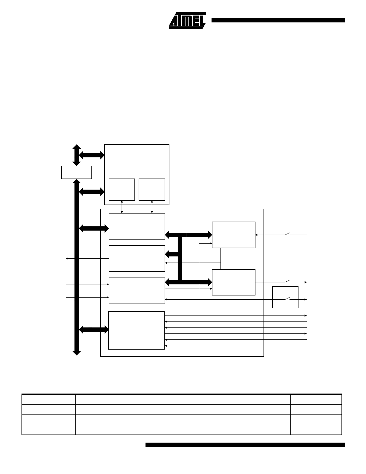
USART: Universal Synchronous/Asynchronous Receiver/Transmitter
The AT75C220 provides two identical full-duplex, universal
synchronous/asynchronous receiver/transmitters as
USART A and USART B. These peripherals sit on the APB
bus but are also connected to the ASB bus (and hence
external memory) via a dedicated DMA.
The main features are:
• Programmable baud rate generator
• Parity, framing and overrun error detection
Figure 15. USART Block Diagram
ASB
AMBA
APB
Peripheral Data Controller
Receive
Channel
Control Logic
Transmit
Channel
• Line break generation and detection
• Automatic echo, local loopback and remote loopback
channel modes
• Multi-drop mode: address detection and generation
• Interrupt generation
• Two dedicated peripheral data controller channels
• 6-, 7- and 8-bit character length
• Modem control signals
USART Channel
Receiver
RXD
USxIRQ
ACLK
ACLK/8
Interrupt Control
Baud Rate Generator
Modem Control
Baud Rate Clock
Transmitter
TXD
PIO A
SCK
NRTS
NCTS
NRI
NDTR
NDSR
NDCD
Pin Description
Each USART channel has external signals as defined in Table 22.
Table 22. USART External Signals
Signal Name Description Typ e
SCK USART Serial Clock. Can be configured as input or output. See US_MR I/O
TXD Transmit Serial Data Output
RXD Receive Serial Data Input
74
AT75C220
Page 75

AT75C220
Table 22. USART External Signals
Signal Name Description Typ e
NRTS Request to Send Output
NCTS Clear to Send Input
NDTR Data Terminal Ready Output
NDSR Data Set Ready Input
NDCD Data Carrier Detect Input
NRI Ring Indicator Input
Note: After a hardware reset, the USART SC and modem pins are not enabled by default (see “PIO: Programmable I/O Controller” on
page 63).
Baud Rate Generator
The baud rate generator provides the bit period clock (the
baud rate clock) to both the receiver and the transmitter.
The baud rate generator can select between external and
internal clock sources. The external clock source is SCK.
The internal clock sources can be either the master clock
ACLK or the master clock divided by 8 (ACLK/8).
Note: In all cases, if an external clock is used, the duration of
each of its levels must be longer than the system clock
(ACLK) period. The external clock frequency must be at
least 2.5 times lower than the system clock.
When the USART is programmed to operate in asynchronous mode (SYNC = 0 in the Mode Register US_MR), the
selected clock is divided by 16 times the value (CD) written
in US_BRGR (Baud Rate Generator Register). If
US_BRGR is set to 0, the baud rate clock is disabled.
nal on the SCK pin. No division is active. The value written
in US_BRGR has no effect.
Baud Rate
Selected Clock
=
16 x CD
When the USART is programmed to operate in synchronous mode (SYNC = 1) and the selected clock is internal
(USCLKS[1] = 0 in the Mode Register US_MR), the baud
rate clock is the internal selected clock divided by the value
written in US_BRGR. If US_BRGR is set to 0, the baud rate
clock is disabled.
Baud Rate
Selected Clock
=
CD
In synchronous mode with external clock selected
(USCLKS[1] = 1), the clock is provided directly by the sig-
Table 23. Clock Generator Table
Required Baud Rate
(bps)
9600 156.25 156 9615.4 15.4 0.16
19200 78.125 78 19230.8 30.8 0.16
CD = 24 x 106/
16 x baud rate Actual CD Actual Baud Rate (bps) Error (bps) % Error
75
Page 76

Table 23. Clock Generator Table
Required Baud Rate
(bps)
CD = 24 x 106/
16 x baud rate Actual CD Actual Baud Rate (bps) Error (bps) % Error
38400 39.06 39 38461.5 61.5 0.16
57600 26.04 26 57692.3 92.3 0.16
115200 13.02 13 115384.6 184.6 0.16
Notes: 1. CD = clock driver
2. For information on obtaining exact baud rates using the value of CD given above, the selected clock frequency must be
23,961,600 Hz (23.9616 MHz).
Figure 16. Baud Rate Generator
USCLKS [0]
MCKI
MCKI/8
SCK
0
1
USCLKS [1]
0
CLK
1
CD
16-bit Counter
OUT
0
SYNC
USCLKS [1]
CD
>1
SYNC
1
0
0
Divide
by 16
1
0
Baud Rate
1
Clock
76
AT75C220
Page 77
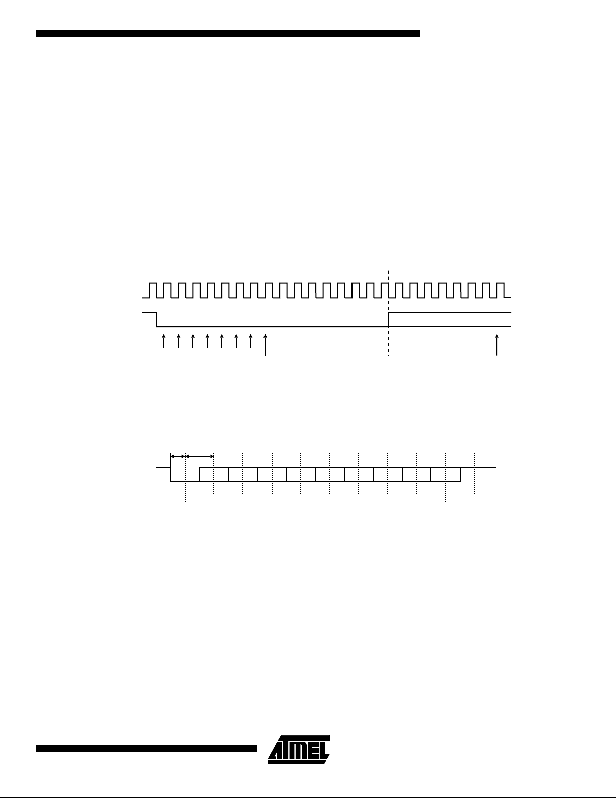
Receiver
Asynchronous Receiver
The USART is configured for asynchronous operation
when SYNC = 0 (bit 7 of US_MR). In asynchronous mode,
the USART detects the start of a received character by
sampling the RXD signal until it detects a valid start bit. A
low level (space) on RXD is interpreted as a valid start bit if
it is detected for more than seven cycles of the sampling
clock, which is 16 times the baud rate. Hence, a space
which is longer than 7/16 of the bit period is detected as a
valid start bit. A space which is 7/16 of a bit period or
Figure 17. Asynchronous Mode: Start Bit Detection
16 x Baud
Rate Clock
RXD
AT75C220
shorter is ignored and the receiver continues to wait for a
valid start bit.
When a valid start bit has been detected, the receiver samples the RXD at the theoretical mid-point of each bit. It is
assumed that each bit lasts 16 cycles of the sampling clock
(1-bit period) so the sampling point is eight cycles (0.5-bit
periods) after the start of the bit. The first sampling point is
therefore 24 cycles (1.5-bit periods) after the falling edge of
the start bit was detected. Each subsequent bit is sampled
16 cycles (1-bit period) after the previous one.
Sampling
True Start
Detection
Figure 18. Asynchronous Mode: Character Reception
Example: 8-bit, parity enabled 1 stop
0.5-bit
periods
RXD
Sampling
1-bit
period
D0 D1 D2 D3 D4 D5 D6 D7
True Start Detection
Synchronous Receiver
When configured for synchronous operation (SYNC = 1),
the receiver samples the RXD signal on each rising edge of
the baud rate clock. If a low level is detected, it is considered as a start. Data bits, parity bit and stop bit are sampled and the receiver waits for the next start bit. See the
example in Figure 19.
Receiver Ready
When a complete character is received, it is transferred to
the US_RHR and the RXRDY status bit in US_CSR is set.
If US_RHR has not been read since the last transfer, the
OVRE status bit in US_CSR is set.
D0
Stop Bit
Parity Bit
Parity Error
Each time a character is received, the receiver calculates
the parity of the received data bits in accordance with the
field PAR in US_MR. It then compares the result with the
received parity bit. If different, the parity error bit PARE in
US_CSR is set.
Framing Error
If a character is received with a stop bit at low level and
with at least one data bit at high level, a framing error is
generated. This sets FRAME in US_CSR.
77
Page 78
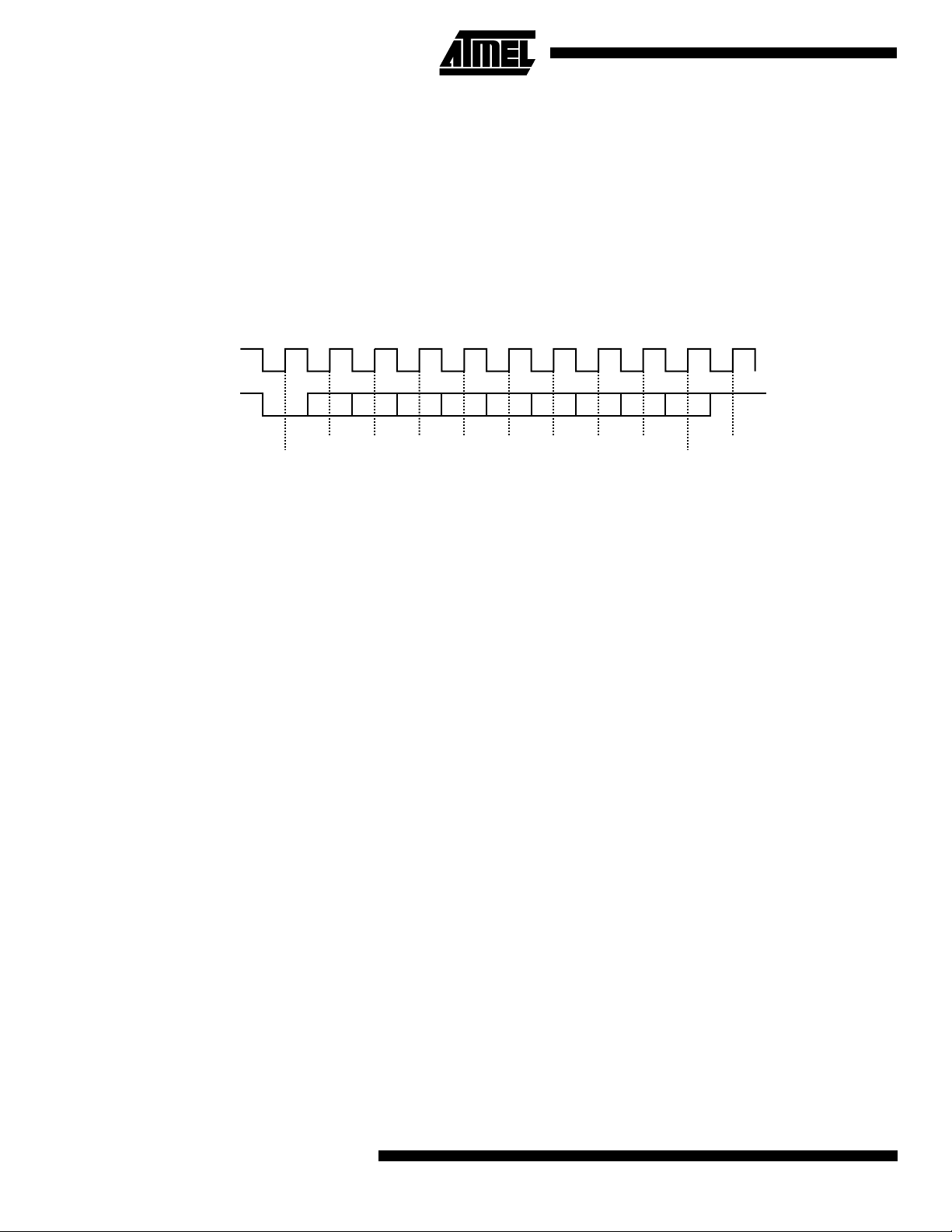
Time-out
This function allows an idle condition on the RXD line to be
detected. The maximum delay for which the USART should
wait for a new character to arrive while the RXD line is inactive (high level) is programmed in US_RTOR. When this
register is set to 0, no time-out is detected. Otherwise, the
receiver waits for a first character and then initializes a
counter which is decremented at each bit period and
reloaded at each byte reception. When the counter reaches
Figure 19. Synchronous Mode: Character Transmission
Example: 8-bit, parity enabled 1 stop
SCK
RXD
0, the TIMEOUT bit in US_CSR is set. The user can restart
the wait for a first character with the STTTO (Start Timeout) bit in US_CR.
Calculation of time-out duration:
Duration Value 4
× Bit Period×=
Sampling
True Start Detection
D0 D1 D2 D3 D4 D5 D6 D7
Transmitter
The transmitter has the same behavior in both synchronous and asynchronous operating modes. Start bit, data
bits, parity bit and stop bits are serially shifted, lowest significant bit first, on the falling edge of the serial clock. See
the example in Figure 20.
The number of data bits is selected in the CHRL field in
US_MR.
The parity bit is set according to the PAR field in US_MR.
The number of stop bits is selected in the NBSTOP field in
US_MR.
When a character is written to US_THR, it is transferred to
the Shift Register as soon as it is empty. When the transfer
occurs, the TXRDY bit in US_CSR is set until a new character is written to US_THR. If the Transmit Shift Register
and US_THR are both empty, the TXEMPTY bit in
US_CSR is set.
Time-guard
The time-guard function allows the transmitter to insert an
idle state on the TXD line between two characters. The
duration of the idle state is programmed in US_TTGR.
Stop Bit
Parity Bit
When this register is set to zero, no time-guard is generated. Otherwise, the transmitter holds a high level on TXD
after each transmitted byte during the number of bit periods
programmed in US_TTGR.
Idle state duration
between two characters
=
Time-guard
value
x
Bit
period
Multi-drop Mode
When the field PAR in US_MR equals 11X (binary value),
the USART is configured to run in multi-drop mode. In this
case, the parity error bit PARE in US_CSR is set when data
is detected with a parity bit set to identify an address byte.
PARE is cleared with the Reset Status Bits Command
(RSTSTA) in US_CR. If the parity bit is detected low, identifying a data byte, PARE is not set.
The transmitter sends an address byte (parity bit set) when
a Send Address Command (SENDA) is written to US_CR.
In this case, the next byte written to US_THR will be transmitted as an address. After this, any byte transmitted will
have the parity bit cleared.
78
AT75C220
Page 79

Figure 20. Synchronous and Asynchronous Mode: Character Transmission
Example: 8-bit, parity enabled 1 stop
Baud Rate
Clock
TXD
AT75C220
Start
D0 D1 D2 D3 D4 D5 D6 D7
Bit
Break
A break condition is a low signal level which has a duration
of at least one character, including start/stop bits and parity.
Transmit Break
The transmitter generates a break condition on the TXD
line when STTBRK is set in US_CR. In this case, the character present in the Transmit Shift Register is completed
before the line is held low.
To cancel a break condition on the TXD line, the STPBRK
command in US_CR must be set. The USART completes a
minimum break duration of one character length. The TXD
line then returns to high level (idle state) for at least 12 bit
periods to ensure that the end of break is correctly
detected. Then the transmitter resumes normal operation.
The break is managed like a character:
• The STTBRK and the STPBRK commands are
performed only if the transmitter is ready (bit TXRDY = 1
in US_CSR).
• The STTBRK command blocks the transmitter holding
register (bit TXRDY is cleared in US_CSR) until the
break has started.
• A break is started when the Shift Register is empty (any
previous character is fully transmitted).
US_CSR.TXEMPTY is cleared. The break blocks the
transmitter shift register until it is completed (high level
for at least 12 bit periods after the STPBRK command is
requested).
In order to avoid unpredictable states:
• STTBRK and STPBRK commands must not be
requested at the same time.
• Once an STTBRK command is requested, further
STTBRK commands are ignored until the break is ended
(high level for at least 12 bit periods).
• All STPBRK commands requested without a previous
STTBRK command are ignored.
• A byte written into the Transmit Holding Register while a
break is pending but not started (bit TXRDY = 0 in
US_CSR) is ignored.
Parity
• It is not permitted to write new data in the Transmit
Bit
Stop
Bit
Holding Register while a break is in progress (STPBRK
has not been requested), even though TXRDY = 1 in
US_CSR.
• A new STTBRK command must not be issued until an
existing break has ended (TXEMPTY = 1 in US_CSR).
The standard break transmission sequence is:
1. Wait for the transmitter ready
(US_CSR.TXRDY = 1).
2. Send the STTBRK command
(write 0x0200 to US_CR).
3. Wait for the transmitter ready
(bit TXRDY = 1 in US_CSR).
4. Send the STPBRK command
(write 0x0400 to US_CR).
The next byte can then be sent:
5. Wait for the transmitter ready
(bit TXRDY = 1 in US_CSR).
6. Send the next byte
(write byte to US_THR).
Each of these steps can be scheduled by using the interrupt if the bit TXRDY in US_IMR is set.
For character transmission, the USART channel must be
enabled before sending a break.
Receive Break
The receiver detects a break condition when all data, parity
and stop bits are low. When the low stop bit is detected, the
receiver asserts the RXBRK bit in US_CSR. An end-ofreceive break is detected by a high level for at least 2/16 of
a bit period in asynchronous operating mode or at least one
sample in synchronous operating mode. RXBRK is also
asserted when an end-of-break is detected.
Both the beginning and the end of a break can be detected
by interrupt if the bit RXBRK in register US_IMR is set.
79
Page 80

Interrupt Generation
Each status bit in US_CSR has a corresponding bit in
US_IER and US_IDR that controls the generation of interrupts by asserting the USART interrupt line connected to
the AIC. US_IMR indicates the status of the corresponding
bits.
When a bit is set in US_CSR and the same bit is set in
US_IMR, the interrupt line is asserted.
Channel Modes
The USART can be programmed to operate in three different test modes using the field CHMODE in US_MR.
Automatic echo mode allows bit-by-bit re-transmission.
When a bit is received on the RXD line, it is sent to the TXD
line. Programming the transmitter has no effect.
Local loopback mode allows the transmitted characters to
be received. TXD and RXD pins are not used and the output of the transmitter is internally connected to the input of
the receiver. The RXD pin level has no effect and the TXD
pin is held high, as in idle state.
Remote loopback mode directly connects the RXD pin to
the TXD pin. The transmitter and the receiver are disabled
and have no effect. This mode allows bit-by-bit re-transmission.
Figure 21. Channel Modes
Automatic Echo
Receiver
Transmitter
Local Loopback
Receiver
Transmitter
Remote Loopback
Receiver
Disabled
V
DD
Disabled
Disabled
Disabled
RXD
TXD
RXD
V
DD
TXD
RXD
Transmitter
Disabled
TXD
80
AT75C220
Page 81

AT75C220
Peripheral Data Controller
Each USART channel is closely connected to a corresponding peripheral data controller channel. One is dedicated to the receiver, the other is dedicated to the transmitter.
Note: The PDC is disabled if 9-bit character length is selected
(MODE9 = 1) in US_MR.
The PDC channel is programmed using US_TPR and
US_TCR for the transmitter and US_RPR and US_RCR for
the receiver. The status of the PDC is given in US_CSR by
the ENDTX bit for the transmitter and by the ENDRX bit for
the receiver.
The pointer registers US_TPR and US_RPR are used to
store the address of the transmit or receive buffers. The
counter registers US_TCR and US_RCR are used to store
the size of these buffers.
The receiver data transfer is triggered by the RXRDY bit
and the transmitter data transfer is triggered by TXRDY.
When a transfer is performed, the counter is decremented
and the pointer is incremented. When the counter reaches
0, the status bit is set (ENDRX for the receiver, ENDTX for
the transmitter in US_CSR) and can be programmed to
generate an interrupt. Transfers are then disabled until a
new non-zero counter value is programmed.
Modem Control and Status Signals
NCTS: Clear to Send
When low, this indicates that the modem or data set is
ready to exchange data. The NCTS signal is a modem status input whose conditions can be tested by the CPU
reading bit 4 (CTS) of the Modem Status Register. Bit 4 is
the complement of the NCTS signal. Bit 0 (DCTS) of the
Modem Status Register indicates whether the NCTS input
has changed state since the previous reading of the
Modem Status Register. NCTS has no effect on the
transmitter.
In FCM mode when the NCTS signal becomes inactive
high, the transmission of the current character will be completed then transmission stops.
Note: Whenever the CTS bit of the Modem Status Register
changes state, an interrupt is generated if the Modem
Status Interrupt is enabled.
NDCD: Data Carrier Detect
When low, this indicates that the data carrier has been
detected by the modem or data set. The NDCD signal is a
modem status input whose condition can be tested by the
CPU reading bit 7 (DCD) of the Modem Status Register. Bit
7 is the complement of the NDCD signal. Bit 3 (DDCD) of
the Modem Status Register indicates whether the NDCD
input pin has changed since the previous reading of the
Modem Status Register. NDCD has no effect on the
receiver.
Note: Whenever the DCD bit of the Modem Status Register
changes state, an interrupt is generated if the Modem
Status Interrupt is enabled.
NDSR: Data Set Ready
When low, this informs the modem or data set the USART
is ready to communicate. The NDSR signal is a modem
status input whose condition can be tested by the CPU
reading bit 5 (DSR) of the Modem Status Register. Bit 5 is
the complement of the NDSR signal. Bit 1 (DDSR of the
Modem Status Register) indicates whether the NDSR input
has changed state since the previous reading of the
Modem Status Register.
Note: Whenever the DSSR bit of the Modem Status Register
changes state, an interrupt is generated if the Modem
Status Interrupt is enabled.
NDTR: Data Terminal Ready
When low, this informs the modem or data set that the
USART is ready to communicate. The NDTR output signal
can be set to active low by programming bit 0 (DTR) of the
Modem Control Register to a high level. A master reset
operation sets this signal to its inactive (high) state. Loop
mode operation holds this signal in its inactive state.
NRI: Ring Indicator
When low, this indicates that a telephone ringing signal has
been received by the modem or data set. The NRI signal is
a modem status input whose condition can be tested by the
CPU reading bit 6 (RI) of the Modem Status Register. Bit 6
is the complement of the NRI signal. Bit 2 (TERI) of the
Modem Status Register indicates whether the NRI input
signal has changed from a low to a high state since the previous reading of the Modem Status Register.
Note: Whenever the RI bit of the Modem Status Register
changes from a high to a low state, an interrupt is generated if the Modem Status Interrupt is enabled.
NRTS: Request to Send
When low, this informs the modem or data set that the
USART is ready to exchange data. The NRTS output signal
can be set to an active low by programming bit 1 (RTS) of
the Modem Control Register. A master reset operation sets
this signal to its inactive (high) state. In FCM mode when
the last stop bit of a character is transmitted and the Transmit Holding Register is empty, the hardware sets NRTS
inactive high.
Note: Modem control pins must be left high when not used.
81
Page 82

USART User Interface
Base Address USART A: 0xFF018000
Base Address USART B: 0xFF01C000
Offset Register Name Description Access Reset Value
0x00 US_CR
0x04 US_MR
0x08 US_IER
0x0C US_IDR
0x10 US_IMR
0x14 US_CSR
0x18 US_RHR
0x1C US_THR
0x20 US_BRGR
0x24 US_RTOR
0x28 US_TTGR
0x2C
0x30 US_RPR
0x34 US_RCR
0x38 US_TPR
0x3C US_TCR
–
Control Register
Mode Register
Interrupt Enable Register
Interrupt Disable Register
Interrupt Mask Register
Channel Status Register
Receiver Holding Register
Transmitter Holding Register
Baud Rate Generator Register
Receiver Time-out Register
Transmitter Time-guard Register
Reserved
Receive Pointer Register
Receive Counter Register
Transmit Pointer Register
Transmit Counter Register
Write-only –
Read/write 0
Write-only –
Write-only –
Read-only 0
Read-only 0x18
Read-only 0
Write-only –
Read/write 0
Read/write 0
Read/write 0
–
Read/write 0
Read/write 0
Read/write 0
Read/write 0
(1)
–
0x40 US_MC
0x44 US_MS
Notes: 1. This is either 0x18 or 0x418 depending on the value of bootn and modem control inputs.
2. This depends on the value of modem control input signals, as these are reflected in this register.
Modem Control Register
Modem Status Register
Write-only –
Read-only (See Note 2)
82
AT75C220
Page 83

AT75C220
USART Control Register
Name: US_CR
Access Type:Write-only
Reset Value:Undefined
31 30 29 28 27 26 25 24
––––––––
23 22 21 20 19 18 17 16
––––––––
15 14 13 12 11 10 9 8
–––SENDA STTTO STPBRK STTBRK RSTSTA
76543210
TXDIS TXEN RXDIS RXEN RSTTX RSTRX ––
• RSTRX: Reset Receiver
0 = No effect.
1 = The receiver logic is reset.
• RSTTX: Reset Transmitter
0 = No effect.
1 = The transmitter logic is reset.
• RXEN: Receiver Enable
0 = No effect.
1 = The receiver is enabled if RXDIS is 0.
• RXDIS: Receiver Disable
0 = No effect.
1 = The receiver is disabled.
• TXEN: Transmitter Enable
0 = No effect.
1 = The transmitter is enabled if TXDIS is 0.
• TXDIS: Transmitter Disable
0 = No effect.
1 = The transmitter is disabled.
• RSTSTA: Reset Status Bits
0 = No effect.
1 = Resets the status bits PARE, FRAME, OVRE and RXBRK in the US_CSR.
• STTBRK: Start Break
0 = No effect.
1 = If break is not being transmitted, starts transmission of a break after the characters present in US_THR and the
Transmit Shift Register have been transmitted.
• STPBRK: Stop Break
0 = No effect.
1 = If a break is being transmitted, stops transmission of the break after a minimum of one character length and trans-
mits a high level during 12 bit periods.
• STTTO: Start Time-out
0 = No effect.
1 = Starts waiting for a character before clocking the time-out counter.
• SENDA: Send Address
0 = No effect.
83
Page 84

1 = In multi-drop mode only, the next character written to the US_THR is sent with the address bit set.
84
AT75C220
Page 85

USART Mode Register
Name: US_MR
Access Type:Read/write
Reset Value:0x0
31 30 29 28 27 26 25 24
––––––––
23 22 21 20 19 18 17 16
–––––CLKO MODE9 –
15 14 13 12 11 10 9 8
CHMODE NBSTOP PAR SYNC
76543210
CHRL USCLKS ––––
• USCLKS: Clock Selection (Baud Rate Generator Input Clock)
USCLKS Selected Clock
AT75C220
00
01
1X
ACLK
ACLK/8
External (SCK)
• CHRL: Character Length
Start, stop and parity bits are added to the character length.
CHRL Character Length
00
01
10
11
Five bits
Six bits
Seven bits
Eight bits
• SYNC: Synchronous Mode Select
0 = USART operates in asynchronous mode.
1 = USART operates in synchronous mode.
• PAR: Parity Type
PAR P a r i t y Ty pe
000
001
010
011
10x
11x
Even parity
Odd parity
Parity forced to 0 (space)
Parity forced to 1 (mark)
No parity
Multi-drop mode
85
Page 86

• NBSTOP: Number of Stop Bits
The interpretation of the number of stop bits depends on SYNC.
NBSTOP
0 0 1 stop bit 1 stop bit
0 1 1.5 stop bits Reserved
1 0 2 stop bits 2 stop bits
1 1 Reserved Reserved
Asynchronous
(SYNC = 0)
Synchronous
(SYNC = 1)
• CHMODE: Channel Mode
CHMODE Mode Description
0 0 Normal Mode
0 1 Automatic Echo
1 0 Local Loopback
1 1 Remote Loopback
The USART channel operates as an Rx/Tx USART.
Receiver data input is connected to TXD pin.
Transmitter output signal is connected to receiver input signal.
RXD pin is internally connected to TXD pin.
• MODE9: 9-bit Character Length
0 = CHRL defines character length.
1 = 9-bit character length.
• CKLO: Clock Output Select
0 = The USART does not drive the SCK pin.
1 = The USART drives the SCK pin if USCLKS[1] is 0.
86
AT75C220
Page 87

AT75C220
USART Interrupt Enable Register
Name: US_IER
Access Type:Write-only
Reset Value: Undefined
31 30 29 28 27 26 25 24
––––––––
23 22 21 20 19 18 17 16
––––––––
15 14 13 12 11 10 9 8
–––––DMSI TXEMPTY TIMEOUT
76543210
PARE FRAME OVRE ENDTX ENDRX RXBRK TXRDY RXRDY
• RXRDY: Enable RXRDY Interrupt
0 = No effect.
1 = Enables RXRDY interrupt.
• TXRDY: Enable TXRDY Interrupt
0 = No effect.
1 = Enables TXRDY interrupt.
• RXBRK: Enable Receiver Break Interrupt
0 = No effect.
1 = Enables receiver break interrupt.
• ENDRX: Enable End of Receive Transfer Interrupt
0 = No effect.
1 = Enables end of receive transfer interrupt.
• ENDTX: Enable End of Transmit Transfer Interrupt
0 = No effect.
1 = Enables end of transmit transfer interrupt.
• OVRE: Enable Overrun Error Interrupt
0 = No effect.
1 = Enables overrun error interrupt.
• FRAME: Enable Framing Error Interrupt
0 = No effect.
1 = Enables framing error interrupt.
• PARE: Enable Parity Error Interrupt
0 = No effect.
1 = Enables parity error interrupt.
• TIMEOUT: Enable Time-out Interrupt
0 = No effect.
1 = Enables reception time-out interrupt.
• TXEMPTY: Enable TXEMPTY Interrupt
0 = No effect.
1 = Enables TXEMPTY interrupt.
• DMSI: Delta Modem Status Indication Interrupt
0 = No effect.
1 = Enables DMSI interrupt.
87
Page 88

USART Interrupt Disable Register
Name: US_IDR
Access Type:Write-only
Reset Value: Undefined
31 30 29 28 27 26 25 24
––––––––
23 22 21 20 19 18 17 16
––––––––
15 14 13 12 11 10 9 8
–––––DMSI TXEMPTY TIMEOUT
76543210
PARE FRAME OVRE ENDTX ENDRX RXBRK TXRDY RXRDY
• RXRDY: Disable RXRDY Interrupt
0 = No effect.
1 = Disables RXRDY interrupt.
• TXRDY: Disable TXRDY Interrupt
0 = No effect.
1 = Disables TXRDY interrupt.
• RXBRK: Disable Receiver Break Interrupt
0 = No effect.
1 = Disables receiver break interrupt.
• ENDRX: Disable End of Receive Transfer Interrupt
0 = No effect.
1 = Disables end of receive transfer interrupt.
• ENDTX: Disable End of Transmit Transfer Interrupt
0 = No effect.
1 = Disables end of transmit transfer interrupt.
• OVRE: Disable Overrun Error Interrupt
0 = No effect.
1 = Disables overrun error interrupt.
• FRAME: Disable Framing Error Interrupt
0 = No effect.
1 = Disables framing error interrupt.
• PARE: Disable Parity Error Interrupt
0 = No effect.
1 = Disables Parity Error Interrupt.
• TIMEOUT: Disable Time-out Interrupt
0 = No effect.
1 = Disables receiver time-out interrupt.
• TXEMPTY: Disable TXEMPTY Interrupt
0 = No effect.
1 = Disables TXEMPTY interrupt.
• DMSI: Delta Modem Status Indication Interrupt
0 = No effect.
1 = Disables DMSI interrupt.
88
AT75C220
Page 89

AT75C220
USART Interrupt Mask Register
Name: US_IMR
Access Type:Read-only
Reset Value: 0x0
31 30 29 28 27 26 25 24
––––––––
23 22 21 20 19 18 17 16
––––––––
15 14 13 12 11 10 9 8
–––––DMSI TXEMPTY TIMEOUT
76543210
PARE FRAME OVRE ENDTX ENDRX RXBRK TXRDY RXRDY
• RXRDY: RXRDY Interrupt Mask
0 = RXRDY interrupt is disabled.
1 = RXRDY interrupt is enabled.
• TXRDY: TXRDY Interrupt Mask
0 = TXRDY interrupt is disabled.
1 = TXRDY interrupt is enabled.
• RXBRK: Receiver Break Interrupt Mask
0 = Receiver break interrupt is disabled.
1 = Receiver break interrupt is enabled.
• ENDRX: End of Receive Transfer Interrupt Mask
0 = End of Receive Transfer Interrupt is disabled.
1 = End of Receive Transfer Interrupt is enabled.
• ENDTX: End of Transmit Transfer Interrupt Mask
0 = End of transmit transfer interrupt is disabled.
1 = End of transmit transfer interrupt is enabled.
• OVRE: Overrun Error Interrupt Mask
0 = Overrun error interrupt is disabled.
1 = Overrun error interrupt is enabled.
• FRAME: Framing Error Interrupt Mask
0 = Framing error interrupt is disabled.
1 = Framing error interrupt is enabled.
• PARE: Parity Error Interrupt Mask
0 = Parity error interrupt is disabled.
1 = Parity error interrupt is enabled.
• TIMEOUT: Time-out Interrupt Mask
0 = Receive time-out interrupt is disabled.
1 = Receive time-out interrupt is enabled.
• TXEMPTY: TXEMPTY Interrupt Mask
0 = TXEMPTY interrupt is disabled.
1 = TXEMPTY interrupt is enabled.
• DMSI: Delta Modem Status Indication Interrupt
0 = DMSI interrupt is disabled.
1 = DMSI interrupt is enabled.
89
Page 90

USART Channel Status Register
Name: US_CSR
Access Type:Read-only
Reset Value: 0x18
31 30 29 28 27 26 25 24
––––––––
23 22 21 20 19 18 17 16
––––––––
15 14 13 12 11 10 9 8
–––––DMSI TXEMPTY TIMEOUT
76543210
PARE FRAME OVRE ENDTX ENDRX RXBRK TXRDY RXRDY
• RXRDY: Receiver Ready
0 = No complete character has been received since the last read of the US_RHR or the receiver is disabled.
1 = At least one complete character has been received and the US_RHR has not yet been read.
• TXRDY: Transmitter Ready
0 = US_THR contains a character waiting to be transferred to the Transmit Shift Register.
1 = US_THR is empty and there is no break request pending TSR availability.
Equal to zero when the USART is disabled or at reset. Transmitter enable command (in US_CR) sets this bit to one.
• RXBRK: Break Received/End of Break
0 = No break received or end of break detected since the last reset status bits command in the Control Register.
1 = Break received or end of break detected since the last reset status bits command in the Control Register.
• ENDRX: End-of-receive Transfer
0 = The end-of-transfer signal from the PDC channel dedicated to the receiver is inactive.
1 = The end-of-transfer signal from the PDC channel dedicated to the receiver is active.
• ENDTX: End-of-transmit Transfer
0 = The end-of-transfer signal from the PDC channel dedicated to the transmitter is inactive.
1 = The end-of-transfer signal from the PDC channel dedicated to the transmitter is active.
• OVRE: Overrun Error
0 = No byte has been transferred from the Receive Shift Register to the US_RHR when RxRDY was asserted since the
last reset status bits command.
1 = At least one byte has been transferred from the Receive Shift Register to the US_RHR when RxRDY was asserted
since the last reset status bits command.
• FRAME: Framing Error
0 = No stop bit has been detected low since the last reset status bits command.
1 = At least one stop bit has been detected low since the last reset status bits command.
• PARE: Parity Error
1 = At least one parity bit has been detected false (or a parity bit high in multi-drop mode) since the last reset status bit”
command.
0 = No parity bit has been detected false (or a parity bit high in multi-drop mode) since the last reset status bits
command.
• TIMEOUT: Receiver Time-out
0 = There has not been a time-out since the last start time-out command or the Time-out Register is 0.
1 = There has been a time-out since the last start time-out command.
90
AT75C220
Page 91

AT75C220
• TXEMPTY: Transmitter Empty
0 = There are characters in either US_THR or the Transmit Shift Register or a break is being transmitted.
1 = There are no characters in US_THR and the Transmit Shift Register and break is not active.
Equal to zero when the USART is disabled or at reset. Transmitter enable command (in US_CR) sets this bit to one.
• DMSI: Delta Modem Status Indication Interrupt
0 = No effect.
1 = There has been a change in the modem status delta bits since the last reset status bits command.
USART Receiver Holding Register
Name: US_RHR
Access Type:Read-only
Reset Value: 0x0
31 30 29 28 27 26 25 24
––––––––
23 22 21 20 19 18 17 16
––––––––
15 14 13 12 11 10 9 8
–––––––RXCHR
76543210
RXCHR
• RXCHR: Received Character
Last character received if RXRDY is set. When number of data bits is less than eight, the bits are right-aligned.
All unused bits read as zero.
USART Transmitter Holding Register
Name: US_THR
Access Type:Write-only
Reset Value: Undefined
31 30 29 28 27 26 25 24
––––––––
23 22 21 20 19 18 17 16
––––––––
15 14 13 12 11 10 9 8
–––––––TXCHR
76543210
TXCHR
• TXCHR: Character to be Transmitted
Next character to be transmitted after the current character if TXRDY is not set. When number of data bits is less than
eight, the bits are right-aligned.
91
Page 92

USART Baud Rate Generator Register
Name: US_BRGR
Access Type:Read/write
Reset Value: 0x0
31 30 29 28 27 26 25 24
––––––––
23 22 21 20 19 18 17 16
––––––––
15 14 13 12 11 10 9 8
CD
76543210
CD
• CD: Clock Divisor
This register has no effect if synchronous mode is selected with an external clock.
CD Effect
0
1
2 to 65535 Baud rate (asynchronous mode) = Selected clock/(16 x CD)
Note: In synchronous mode, the value programmed must be even to ensure a 50:50 mark-to-space ratio.
Note: Clock divisor bypass (CD = 1) must not be used when internal clock ACLK is selected (USCLKS = 0).
Disables clock
Clock divisor bypass
Baud rate (synchronous mode) = Selected clock/CD
92
AT75C220
Page 93
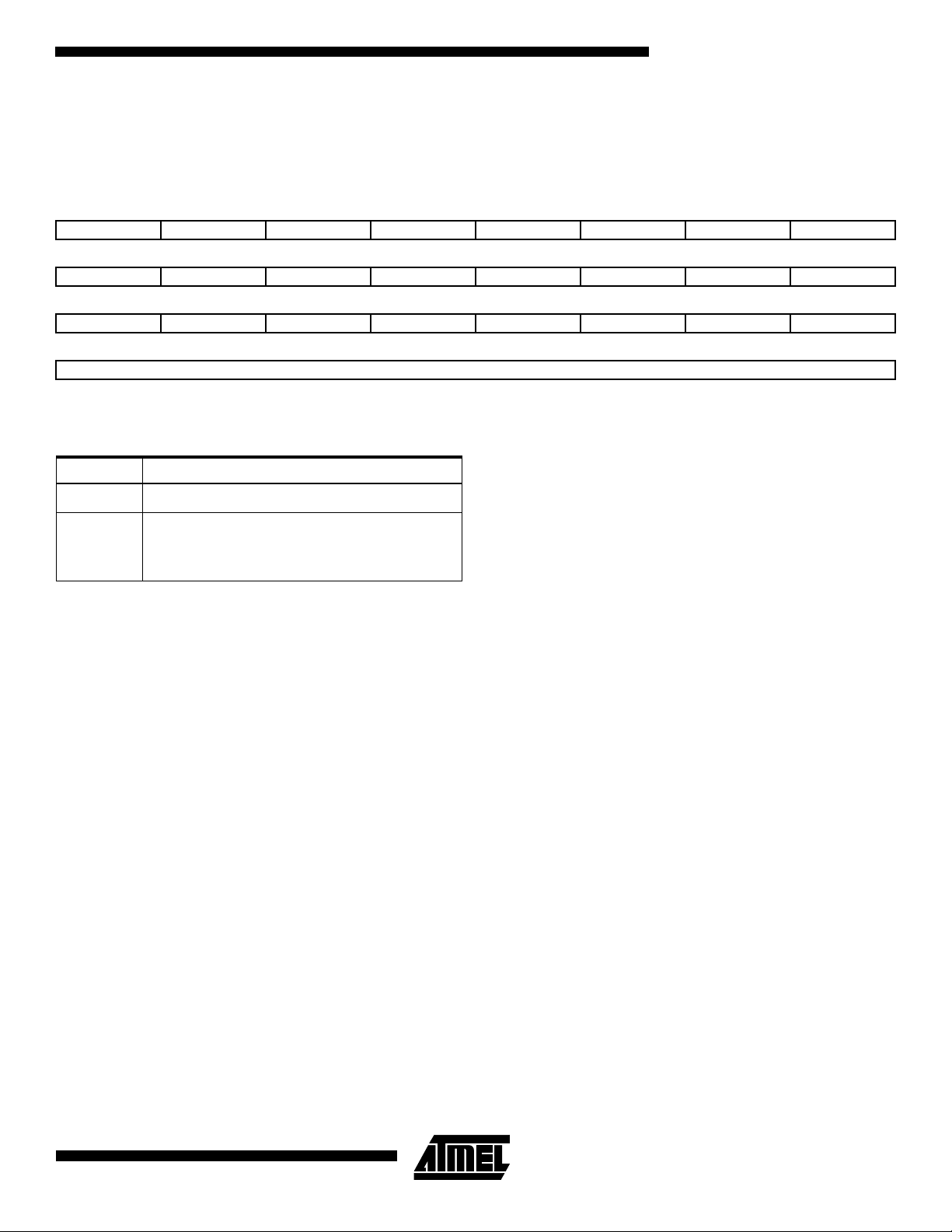
AT75C220
USART Receiver Time-out Register
Name: US_RTOR
Access Type:Read/write
Reset Value: 0x0
31 30 29 28 27 26 25 24
––––––––
23 22 21 20 19 18 17 16
––––––––
15 14 13 12 11 10 9 8
––––––––
76543210
TO
• TO: Time-out Value
When a value is written to this register, a start time-out command is automatically performed.
TO Effect
0
1 - 255 The time-out counter is loaded with TO when the
Disables the RX time-out function.
start time-out command is given or when each
new data character is received (after reception
has started).
Time-out duration = TO x 4 x Bit period
93
Page 94

USART Transmitter Time-guard Register
Name: US_TTGR
Access Type:Read/write
Reset Value: 0x0
31 30 29 28 27 26 25 24
––––––––
23 22 21 20 19 18 17 16
––––––––
15 14 13 12 11 10 9 8
––––––––
76543210
• TG: Time-guard Value
TG Effect
TG
0
1 - 255
Disables the TX time-guard function.
TXD is inactive high after the transmission of
each character for the time-guard duration.
Time-guard duration = TG x Bit period
USART Receive Pointer Register
Name: US_RPR
Access Type:Read/write
Reset Value: 0x0
31 30 29 28 27 26 25 24
23 22 21 20 19 18 17 16
15 14 13 12 11 10 9 8
76543210
• RXPTR: Receive Pointer
RXPTR must be loaded with the address of the receive buffer.
RXPTR
RXPTR
RXPTR
RXPTR
94
AT75C220
Page 95

USART Receive Counter Register
Name: US_RCR
Access Type:Read/write
Reset Value: 0x0
31 30 29 28 27 26 25 24
––––––––
23 22 21 20 19 18 17 16
––––––––
15 14 13 12 11 10 9 8
76543210
• RXCTR: Receive Counter
RXCTR must be loaded with the size of the receive buffer.
0: Stop peripheral data transfer dedicated to the receiver.
1 - 65535: Start peripheral data transfer if RXRDY is active.
AT75C220
RXCTR
RXCTR
USART Transmit Pointer Register
Name: US_TPR
Access Type:Read/write
Reset Value: 0x0
31 30 29 28 27 26 25 24
23 22 21 20 19 18 17 16
15 14 13 12 11 10 9 8
76543210
• TXPTR: Transmit Pointer
TXPTR must be loaded with the address of the transmit buffer.
TXPTR
TXPTR
TXPTR
TXPTR
95
Page 96

USART Transmit Counter Register
Name: US_TCR
Access Type:Read/write
Reset Value: 0x0
31 30 29 28 27 26 25 24
––––––––
23 22 21 20 19 18 17 16
––––––––
15 14 13 12 11 10 9 8
76543210
• TXCTR: Transmit Counter
TXCTR must be loaded with the size of the transmit buffer.
0: Stop peripheral data transfer dedicated to the transmitter.
1 - 65535: Start peripheral data transfer if TXRDY is active.
TXCTR
TXCTR
96
AT75C220
Page 97

AT75C220
Modem Control Register
Register Name:US_MC
Access Type:Write-only
Reset Value: Undefined
31 30 29 28 27 26 25 24
––––––––
23 22 21 20 19 18 17 16
––––––––
15 14 13 12 11 10 9 8
––––––––
76543210
––FCM –––RTS DTR
This register controls the interface with the modem or data set (or a peripheral device emulating a modem). The contents of
the Control Register are indicated below.
• DTR: Data Terminal Ready
This bit controls the NDTR output. When bit 0 is set to a logic 1, the NDTR output is forced to a logic 0.
When bit 0 is reset to a logic 0, the NDTR output is forced to a logic 1.
Note: The NDTR output of the UART can be applied to an EIA inverting line driver to obtain proper polarity input at the succeeding
modem or data set.
• RTS: Request to Send
This bit controls the NRTS output. Bit 1 affects the NRTS output in a manner identical to that described above for bit 0.
• FCM: Flow Control Mode
When FCM is set high, the hardware can perform operations automatically depending on the state of NCTS and character transmission logic. Such changes take place immediately and are reflected in the values read in the Modem
Status Register. This flag is set low at reset.
In flow control mode, transmission should occur only if NCTS is active.
97
Page 98

Modem Status Register
Register Name:US_MS
Access Type:Read-only
Reset Value:Undefined
31 30 29 28 27 26 25 24
––––––––
23 22 21 20 19 18 17 16
––––––––
15 14 13 12 11 10 9 8
–––––––FCMS
76543210
DCD RI DSR CTS DDCD TERI DDSR DCTS
This register provides the current state of the control lines from the modem (or peripheral device) to the CPU. In addition to
this current-state information, four bits of the Modem Status Register provide change information. These bits are set to a
logic 1 whenever a control input from the modem changes state. They are reset to logic 0 whenever the CPU reads the
Modem Status Register.
• DCTS: Delta Clear to Send
Bit 0 indicates that the NCTS input to the chip has changed state since the last time it was read by the CPU.
• DDSR: Delta Data Set Ready
Bit 1 indicates that the NDSR input to the chip has changed state since the last time it was read by the CPU.
• TERI: Trailing Edge Ring Indicator
Bit 2 indicates that the NRI input to the chip has changed from a low to a high state.
• DDCD: Delta Data Carrier Detect
Bit 3 indicates that the NDCD input has changed state.
Note that whenever bit 0, 1, 2, or 3 is set to logic 1, a modem status interrupt is generated. This is reflected in the modem
status register.
• CTS: Clear to Send
This bit is the complement of the Clear to Send (NCTS) input.
• DSR: Data Set Ready
This bit is the complement of the Data Set Ready (NDSR) input.
• RI: Ring Indicator
This bit is the complement of the Ring Indicator (NRI) input.
• DCD: Data Carrier Detect
This bit is the complement of the Data Carrier Detect (NDCD) input.
• FCMS: Flow Control Status
This bit indicates the value of the FCM in the US_MC.
98
AT75C220
Page 99

TC: Timer/Counter
The AT75C220 features a timer/counter block which
includes three identical 16-bit timer/counter channels. Each
channel can be independently programmed to perform a
wide range of functions including frequency measurement,
event counting, interval measurement, pulse generation,
delay timing and pulse-width modulation.
Each timer/counter channel has three external clock inputs,
five internal clock inputs, and two multi-purpose input/output signals that can be configured by the user. Each chan-
Figure 22. Timer/Counter Block Diagram
ACLK/2
ACLK/8
ACLK/32
ACLK/128
ACLK/1024
TCLK0
TCLK1
TCLK2
TIOA1
TIOA2
XC0
XC1
XC2
TC0XC0S
AT75C220
nel drives an internal interrupt signal that can be programmed to generate processor interrupts via the AIC.
The timer/counter block has two global registers which act
upon all three TC channels. The Block Control Register
allows the three channels to be started simultaneously with
the same instruction. The Block Mode Register defines the
external clock inputs for each timer/counter channel, allowing them to be chained.
Parallel I/O
Timer/Counter
Channel 0
SYNC
TIOA
TIOB
Controller
TIOA0
TIOB0
INT
TCLK0
TCLK1
TCLK2
TIOA0
TIOB0
TCLK0
TCLK1
TIOA0
TIOA2
TCLK2
TCLK0
TCLK1
TCLK2
TIOA0
TIOA1
Timer/Counter Block
XC0
XC1
XC2
TC1XC1S
XC0
XC1
XC2
TC2XC2S
Timer/Counter
Channel 1
SYNC
Timer/Counter
Channel 2
SYNC
TIOA
TIOB
TIOA
TIOB
INT
INT
TIOA1
TIOB1
TIOA2
TIOB2
TIOA1
TIOB1
TIOA2
TIOB2
Advanced
Interrupt
Controller
99
Page 100

Signal Name Description
Channel Signal Description Typ e
XC0, XC1, XC2 External clock inputs I
TIOA
TIOB
INT Interrupt signal output O
SYNC Synchronization input signal I
Block Signal
TCLK0, TCLK1, TCLK2 External clock inputs I
TIOA0 TIOA signal for Channel 0 I/O
TIOB0 TIOB signal for Channel 0 I/O
TIOA1 TIOA signal for Channel 1 I/O
TIOB1 TIOB signal for Channel 1 I/O
TIOA2 TIOA signal for Channel 2 I/O
TIOB2 TIOB signal for Channel 2 I/O
Note: After a hardware reset, the timer/counter block pins are controlled by the PIO controller. They must be configured to be con-
trolled by the peripheral before being used.
Capture mode: General-purpose input
Waveform mode: General-purpose output
Capture mode: General-purpose input
Waveform mode: General-purpose input/output
I
O
I
O
Timer/Counter Description
The three timer/counter channels are independent and
identical in operation. The registers for channel programming are listed in Table 25 on page 106.
Counter
Each timer/counter channel is organized around a 16-bit
counter. The value of the counter is incremented at each
positive edge of the selected clock. When the counter has
reached the value 0xFFFF and passes to 0x0000, an overflow occurs and the bit COVFS in TC_SR (Status Register)
is set.
The current value of the counter is accessible in real time
by reading TC_CV. The counter can be reset by a trigger.
In this case, the counter value passes to 0x0000 on the
next valid edge of the selected clock.
Clock Selection
At block level, input clock signals of each channel can
either be connected to the external inputs TCLK0, TCLK1
or TCLK2, or be connected to the configurable I/O signals
TIOA0, TIOA1 or TIOA2 for chaining by programming the
TC_BMR (Block Mode).
Each channel can independently select an internal or external clock source for its counter:
• Internal clock signals: ACLK/2, ACLK/8, ACLK/32,
ACLK/128, ACLK/1024
• External clock signals: XC0, XC1 or XC2
The selected clock can be inverted with the CLKI bit in
TC_CMR (Channel Mode). This allows counting on the
opposite edges of the clock.
The burst function allows the clock to be validated when an
external signal is high. The BURST parameter in the Mode
Register defines this signal (none, XC0, XC1, XC2).
Note: In all cases, if an external clock is used, the duration of
each of its levels must be longer than the system clock
(ACLK) period. The external clock frequency must be at
least 2.5 times lower than the system clock (ACLK).
100
AT75C220
 Loading...