

Page 1

Features
• Fulfills IEC 1036, Class 1 Accuracy Requirements
• Fulfills IEC 687, Class 0.5 and Class 0.2 Accuracy, with External Temperature
Compensated Voltage Reference
• Fulfills IEC 1268, Requirements for Reactive Power
• Simultaneous Active, Reactive and Apparent Power and Energy Measurement
• Power Factor, Frequency, Voltage and Current Measurement
• Single- and Poly-phase Operation
• Three Basic Operating Modes: Stand-alone Mode, Microprocessor Mode and Multi-
Channel Mode
• Flexible Interfacing, 8-bit Microprocessor Interface, 8-bit Status Output and Eight
Impulse Outputs
• Calibration of Gain and Phase Error
• Compensation of the Non-linearity of Low Power Measurement
• Adjustable Starting Current and Meter Constant
• Measurement Bandwidth of 1000 Hz
• Tamper-proof Design
• Single +5V Supply
Description
A two chip solution, co ns isting of AT73C500 and AT73C501 (or AT 7 3C50 2) , offer s all
main features required for the measurement and calculation of various power and
energy quantiti es in static Watt-h our meters. The dev ices operate acc ording to
IEC1036, class 1, specification. IEC 687, class 0.5 and 0.2 requirements are fulfilled
when used with external temperature compensated voltage reference.
The AT73C501 contains six, high-performance, Sigma-Delta analog-to-digital converters (ADC). The A T73 C500 is an effic ient di gita l si gnal p roc essor (DSP ) that supp orts
interfacing both with the AT73C501 and with an external microprocessor. The
AT73C500 can also be used with the differential input ADC, AT73C502.
With this chipset, only a minimum of discrete components is required to develop products ranging from si mple domestic Wa tt-hour meters to sop histicated indus trial
meters. The chipset can be used in single-phase as well as in poly-phas e systems.
The AT73C500 is easy to configure. By changing the mode of the AT73C500, the
device can be operated in a stand-alone environment or be used with a separate control processor. It is also possible to configure the circuit to perform the functions of
three independent single phase Wh meters.
The chips support calibration of gain and phase error. All calibrations are done in the
digital domain and no trimming components are needed. The calibration coefficients
are either stored in an EEPROM memory or supplied by an external microprocessor.
(continued)
Chipset
Solution for
Watt-hour
Meters
AT73C500 with
AT73C501 or
AT73C502
Rev. 1035B–09/99
1
Page 2
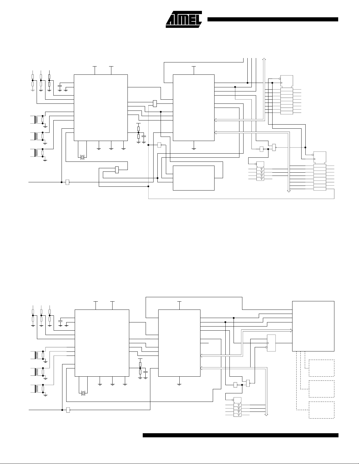
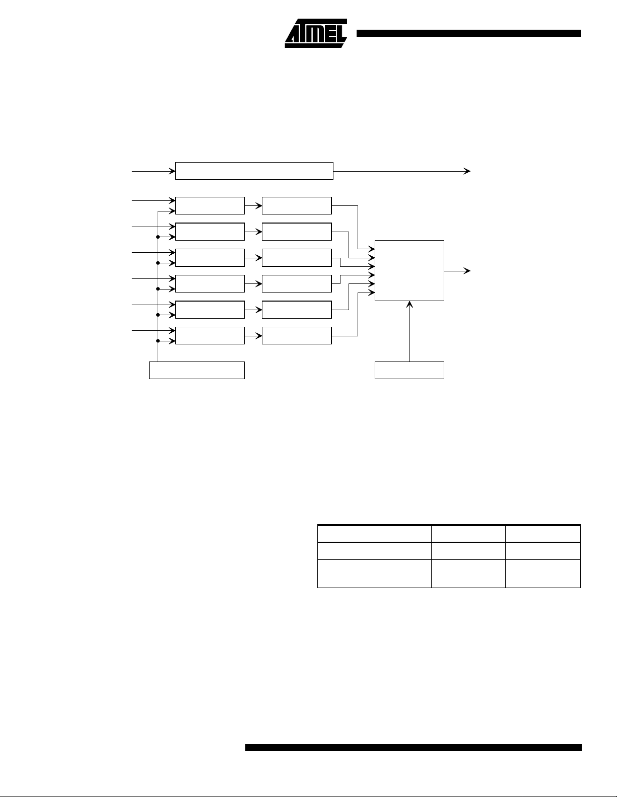
Figure 1. Block diagram of the AT73C500 chipset in stand-alone configuration
EXTERNAL CONNECTOR
L1 L2 L3
L1
L2
L3
RESET
VREF
BGD
AIN2
AIN4
AIN6
AIN1
AIN3
AIN5
RESET
1
CS
VDA
VDDA
AT73C501
SIX SINGLE-ENDED,
INDEPENDENT
SIGMA-DELTA
CONVERTERS
XI XO MODE
VCC
VSA
VSSA
PFAIL
ACK
DATA
CLKR
CLK
AGND
VGND
GND
&
BRDY
IRQ0
IRQ1
&
SIN
SCLK
CLK
XRES
1
CS
SK
The AT73C500 is progr amme d to meas ure act ive, rea ctive
and apparent phase powers. Phase factors, phase voltages, phase currents and line frequenc y are also measured, simultaneously. Based on the individual p hase
powers, total active power is determined.
The power value s are calcul ated over one-line frequency
cycle. The negative and positive results are accumulated in
different registers, which allows for separate billing of
imported and e xported ac tive energ y. Also, the reactive
results are sorted depending on whether capacitive or
inductive load is applied.
VCC
STROBE
RD/WR
DEDICATED DSP
DI
AT73C500
FOR ENERGY
METERING
GND
DGND
AT93C46
EEPROM
128*8 bit
ADDR1
ADDR0
SOUT1
SOUT0
DATA BUS
STATUS BUS
DO
MODE2
MODE1
MODE0
1
1
1
1
1
-VArh
+VArh
-Wh
+Wh
+Wh
-Wh
+VArh
-VArh
&
Eight pulse outputs are provided. Each billing quantity
(+Wh, -Wh, +VArh, -Varh) is supplied with its own meter
constant output, as well as a display counter output. In
multi-channel mode, AT73C500 performs the fu nctions of
three independent s ingle phase Wh me ters and three
impulse outputs are available, one for each meter element.
All measurement inform ation is avai lable on an 8-bit mi croprocessor bus. The results are output in s ix packages, 16
bytes each. Mode and s tatus information of the meter is
also transferred with each data block.
TAMP
STUP
L3
L2
L1
FAIL
DATRDY
INI
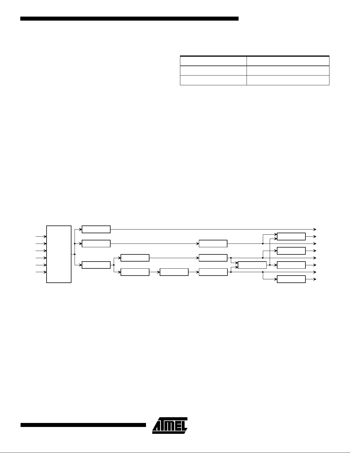
Figure 2. Block diagram of the AT73C500 chipset in microprocessor configuration
L1
L2
L3
RESET
2
L1 L2 L3
VREF
BGD
AIN2
AIN4
AIN6
AIN1
AIN3
AIN5
RESET
1
CS
VDA
VDDA
VCC
AT73501
SIX SINGLE-ENDED,
INDEPENDENT
SIGMA-DELTA
CONVERTERS
XI XO MODE
VSA
VSSA
AT73C500
VGND
GND
PFAIL
ACK
DATA
CLKR
CLK
AGND
BRDY
IRQ0
IRQ1
SCLK
XRES
SIN
VCC
AT73500
DEDICATED DSP
FOR ENERGY
METERING
GND
DGND
STROBE
RD/WR
ADDR1
ADDR0
SOUT1
SOUT0
DATA BUS
STATUS BUS
MODE2
MODE1
MODE0
AT90Sxx
D
DATRDY
B9
&
1
1
1
1
1
B14
B13
B12
MICROCONTROLLER
MODEM
LCD
EEPROM
Page 3
Pin Description
A
A
A
AT73C501 Single-ended ADC
AT73C500
Figure 3. PLCC-28 package pin layout
DAT
FSRACKCLKRCLKXIXO
34
5
BGD
6
CS
7
VCC
VCIN
8
9
10
11
VSSAVDDAAIN2 AIN4 AIN6 AIN1 AIN3
PFAI
AGN
VREF
Power
Supply
Pins Pin I/O Description
VDDA 13 PWR Analog Supply, Positive, +5V
VSSA 12 PWR Analog Supply, Negative, 0V
VDA 21 PWR Analog Supply, Positive, +5V
VSA 20 PWR Analog Supply, Negative, 0V
AGND 9 PWR
VREF 11 PWR
Analog Ground Reference
Input
Referenc e Voltage
Output/Input
VCC 7 PWR Digital Supply, Positive, +5V
VGND 23 PWR Digital Supply, Negative, 0V
Crystal Osc
Signals Pin I/O Description
XI 3 I Crystal Oscillator Input
XO 4 O Crystal Oscillator Output
26272812
25
24
23
22
21
20
19
18171615141312
RESET
N/C
VGND
PD
VD
VS
AIN5
Analog
Signals Pin I/O Description
AIN1 17 I Current, Channel 1
AIN2 14 I Voltage, Channel 1
AIN3 18 I Current, Channel 2
AIN4 15 I Voltage, Channel 2
AIN5 19 I Current, Channel 3
AIN6 16 I Voltage, Channel 3
VCIN 10 I
Input to Voltage Monitoring
Block
Digital
Control
Signals Pin I/O Description
BGD 5 I
By-pass Control
for Reference Voltage
CS 6 I Chip Select Input
PD 22 I
Power Down Control
for A/D Modulators
N/C 24 I Connect to VGND
RESET 25 I Reset Input, Active High
Status
Flags Pin I/O Description
PFAIL 8 O
Output of Voltage Monitoring
Block
Output Bus
Signals Pin I/O Description
CLK 2 O Master Clock Output
CLKR 1 O Serial Bus Clock Output
DATA 26 O Serial Data Output
FSR 27 O
Output Sample Frame
Signal
ACK 28 O
Data Ready Acknowledge
Output
3
Page 4
AT73C502 Differential-Ended ADC
CS
BGD N/C
CLKRCLK
N/CN/CN/C
XI
RESETXO
322
133
4344
42 41 40 39 38 37 36 35 34
DATAACK
FSR
VGND
31
PD
30
VDA
29
VDA
28
VSA
27
VSA
26
SINGLE
25
AIN5N
24
AIN5P
23
AIN3N
1312 14 15 16 17 18 19 20 21 22
VCC
3
VCC
4
PFAIL
5
AGND
6
VCIN
7
VREF
8
N/C
9
VSA
10
VSA
11
AIN1NAIN6NAIN4NAIN2NVDA
AIN3PAIN1PAIN6PAIN4PAIN2PVDA
Figure 4. QFP-44 package pin layout
Power
Supply
Pins Pin I/O Description
VDA
VSA
AGND 6 PWR
VREF 8 PWR
VCC 3, 4 PWR Digital Supply, Positive, +5V
VGND 32 PWR Digital Supply, Negative, 0V
12, 13,
29, 30
10, 11,
27, 28
PWR
PWR
Analog Supply, Positive, +5V
Analog Supply, Negative, 0V
Analog Ground Reference
Input
Referenc e Voltage
Output/Input
Analog
Signals Pin I/O Description
AIN6P 18 I Voltage, Channel 3, Positive
AIN6N 19 I Voltage, Channel 3, Negative
AIN1P 20 I Current, Channel 1, Positive
AIN1N 21 I Current, Channel 1, Negative
AIN3P 22 I Current, Channel 2, Positive
AIN3N 23 I Current, Channel 2, Negative
AIN5P 24 I Current, Channel 3, Positive
AIN5N 25 I Current, Channel 3, Negative
VCIN 7 I
Input to Volta ge Mo nitoring
Block
N/C 9 I Must be left floating
Digital
Control
Signals Pin I/O Description
BGD 1 I
By-pass Control for
Referenc e Voltage
CS 2 I Chip Select Input
PD 31 I
Power Down Control for A/D
Modulators
N/C 33 I Connect to VGND
RESET 34 I Reset Input, Active High
Single / Differential selector.
SINGLE 26 I
· Low: Differential
· High or n/c: Single-ended
Status
Flags Pin I/O Description
Crystal
Osc
Signals Pin I/O Description
XI 43 I Crystal Oscillator Input
XO 44 O Crystal Oscillator Output
Analog
Signals Pin I/O Description
AIN2P 14 I Voltage, Channel 1, Positive
AIN2N 15 I Volta ge, Channel 1, Negative
AIN4P 16 I Voltage, Channel 2, Positive
AIN4N 17 I Volta ge, Channel 2, Negative
4
AT73C500
PFAIL 5 O
Output of V oltage Monitorin g
Block
Output
Bus
Signals Pin I/O Description
CLK 41 O Master Clock Output
CLKR 39 O Serial Bus Clock Output
DATA 35 O Serial Data Output
FSR 36 O
ACK 37 O
Output Sample Frame
Signal
Data Ready Acknowledge
Output
Page 5
AT73C500 DSP
AT73C500
Figure 5. PLCC-44 package pin layout
SOUT15SOUT0
GND
6
GND ADDR0
7 39
B0
8
B1
9
B2
10
GND
11
GND
12
B12
13
B13
14
B14
15
GND
16
B15
17
18
B3
IRQ0 /
GND2GND1CLK44STROBE43VCC42NC41ADDR1
PFAIL
4
3
B419GND20B521B622B723N/C24B825B926GND27B10
40
38
37
36
35
34
33
32
31
30
29
28
Power
Supply
Pins Pin I/O Description
VCC 35, 42 PWR Digital Supply, Positive, +5V
1, 2, 6, 7,
GND
1 1, 12,16,
20, 27, 30,
PWR Digital Supply, Negative, 0V
34
Digital
Inputs Pin I/O Description
CLK 44 I Clock Input
XRES 38 I Reset Input, active low
Interrupt Input, usually
IRQ0 3 I
connected to PF AIL output
of AT73C501
IRQ1 31 I
Interrupt Input, connec ted to
ACK Output of AT73C501
Status/
Mode
Bus Pin I/O Description
B15 17 I/O Status/Mode Bus, Bit7
B14 15 I/O Status/Mode Bus, Bit6
B13 14 I/O Status/Mode Bus, Bit5
B12 13 I/O Status/Mode Bus, Bit4
B11 29 I/O Status/Mode Bus, Bit3
XRES
BRDY
RD/WR
VCC
GND
SIN
SCLK
IRQ1 / ACK
GND
B11
Microprocessor
Bus Pin I/O Description
B7 23 I/O µP Bus, Bit7
B6 22 I/O µP Bus, Bit6
B5 21 I/O µP Bus, Bit5
B4 19 I/O µP Bus, Bit4
B3 18 I/O µP Bus, Bit3
B2 10 I/O µP Bus, Bit2
B1 9 I/O µP Bus, Bit1
B0 8 I/O µP Bus, Bit0
AT73C501 /
AT73C502 and
EEPROM
Interface Pin I/O Description
SOUT0 4 O
Serial Out put, used as a
clock for EEPROM
Serial Output, used as Chip
SOUT1 5 O
Select (CS) for AT73C501
and as Data Input (DI) for
EEPROM
SIN 33 I
SCLK 32 I
Serial Data Input, data from
A T73C501 or from EEPROM
Serial Clock Input, bit clock
from AT73C501
Control Signals
of µP Bus and
Status/Mode
Bus Pin I/O Description
STROBE 43 O Strobe Output
BRDY 37 I
ADDR1 40 O
Microprocessor ready for
I/O, Active Low
Address Output 1, used for
µP bus
Address Output 0, used for
ADDR0 39 O
Status/ Mode bus and for
Impulse Outputs
RD/WR 36 O Read/Write Signal
B10 28 I/O Status/Mode Bus, Bit2
B9 26 I/O Status/Mode Bus, Bit1
B8 25 I/O Status/Mode Bus, Bit0
5
Page 6
AT73C501 and AT73C502
The AT73C501 consi sts o f six, 16 -bit a nalog-to -digi tal c onverters. The converters are equipped with single-ended
inputs. For differenti al ended appli cations, the AT73 C502
chip is used.
Figure 6. Block diagram of the single-ended ADC chip, AT73C501
VOLTAGE
MONITORING
The converters contain a reference volta ge gen erator, vo ltage monitoring bloc k and serial output interf ace. Both c onverters are based on high-performance, oversampling
Sigma-Delta modulators and digital decimation filters.
SIGMA-DELTA
MODULATOR
SIGMA-DELTA
MODULATOR
SIGMA-DELTA
MODULATOR
SIGMA-DELTA
MODULATOR
SIGMA-DELTA
MODULATOR
SIGMA-DELTA
MODULATOR
VOLTAGE
REFERENCE
DECIMATION
FILTER
DECIMATION
FILTER
DECIMATION
FILTER
DECIMATION
FILTER
DECIMATION
FILTER
DECIMATION
FILTER
In a 50 Hz meter, the nominal decimated sampling rate of
3200 Hz is used. This corre spo nds to 64 samples per each
line frequency cycle. 60 Hz meters operate with 3840 Hz
sample rate. The master clock frequency of the ADC is
1024 times higher than the above frequencies, i.e.
3.2768 MHz in 50 Hz meters and 3.93216 MHz in 60 Hz
systems. The default meter constant of AT73C500 energy
counters is based on the above sample rates.
Other sample frequencie s can be used, bu t the energy
results have to be scaled accordingly. If higher sampling
rate is selected, the meter constant will also be increased
by the same ratio.
The three current inputs of AT73C501 are fed from secondary outputs of current transformers, from Hall sensors or
other similar sensors. In differential-ended applications,
such as with current shunt resistors, the AT73C502 ADC
can be used. On both of these converters, the voltage
inputs must be equipped with simple external voltage dividers.
The input voltage range of each converter is 2V
PP
. The
characteristics of a Watt-hour meter operating, according to
IEC1036 specification, are based on a certain basic current, I
. As a default, the basic current of AT73C500
B
chipset is to 6.25% of the current input full scale value. This
means that if a meter is designed for I
= 5A
B
RMS
, the full
scale range of the current channels will be:
SERIAL OUTPUT
LOGIC
TIMING AND
CONTROL
100
IFS = 5 A
-----------
× 80 A
RMS
6.25
=
RMS
The following current transformer and voltage divider configuration is rec ommended fo r a 230V, 3-phas e system,
with 5A basic current:
Voltage Inputs Current Inputs
Converter full-scale input 2.0V
Corresponding full-scale
line voltage / current
270V
PP
RMS
2.0V
80A
PP
RMS
With the above settings, the nominal pulse rate of the
meter constant outp uts is 1250 impulses/kWh (125 0
impulses/kVArh) and the rate of four display outputs 100
impulses/kWh (100 imp/kVArh).
When used in a 5A transformer operated meter, the maximum current range ca n be scaled down to 8A f or exam pl e.
In this case, the me ter constan t will be ten time s higher
than in an 80A meter, i.e. 12500 impulses/kWh. Similarly,
the starting current level will be transferred to 2mA, from
20mA.
6
AT73C500
Page 7
AT73C500
If the nominal voltage is chosen to be 120V, the vo ltage
divider can either have the same config uration as in the
230V meter, or it can be modified to produce 2.0V
pp
with
140V phase voltage. In the latter case, the default meter
constant will be roughly twice the constant of 230V meter,
i.e. 2411 impulses/ kWh. T he mete r cons tant ca n be sca led
to an even number value by means of calibration.
As described above, th e config uration of voltag e divider s
and current tra nsformer s affects to almost all paramet ers
being metered, like energy counters and i mpulse outputs.
A calibration coefficient is provided for the adjustment of
the display pulse rates. With this coefficient, the effect of
various voltage divider and cur rent transformer c onfigurations can be compensated. Care should be tak en that the
dynamic range of the A/D converters is always effectively
utilized. The use o f calibrat ion coeff icients is described in
the next section.
Current and voltage samples of AT73C501/AT73C502 are
multiplexed and transferred to AT73C500 through a serial
interface. The ti ming of the interf ace is presented in the
next section.
AT73C501/AT73C502 con tain a n int ernal b andgap vol tage
reference. When used in cl ass 0.5 and 0.2 me ters, smaller
temperature drift is required. This can be achieved by
bypassing the internal reference and using temperature
compensated external reference instead. The reference is
selected with the BGD input.
BGD Reference
0 (V
) Internal
SS
1 (VDD)External
There is an integrated volt age mo ni torin g blo ck on the converter chip. The PFAIL output is forced high if the level of
voltage supplied to V
input drops below 4.2V. There is a
CIN
hysteresis in the monitoring function and PFAIL returns low
if voltage at V
is raised back above 4.3V.
CIN
PFAIL output of AT73C501/AT73C502 can be connected
to an interrupt input o f AT73C500. A T73C500 detects the
rising edge of PFAIL. To as sure reliable power-down procedure after voltage break, the V
supply of AT73C500
CC
must be equipped with a 470 µF or larger capacitor.
AT73C500
AT73C500 performs p ower and en er gy c alc ulati ons . It a lso
controls the interfacing to the AT73C501 (or AT 73C502)
and to an external microprocessor. The block diagram of
the DSP is presented below.
Figure 7. Block diagram of DSP software
FREQUENCY
MEASUREMENT
u1(n)
u2(n)
u3(n)
i1(n)
i2(n)
i3(n)
DC OFFSET
SUPPRESSION
VOLTAGE
MEASUREMENT
PHASE
CALIBRATION
ACTIVE POWER
MEASUREMENT
HILBERT
TRANSFORM
REACTIVE POWER
MEASUREMENT
Serial Bus Interface
The timing of the serial b us interface c onnecting the AD C
and DSP devices is presented in Figure 8. The same bus is
used to read the calibration data from an ex ternal
EEPROM. This operation is described in section “Loading
of Calibration Coefficients” on page 19.
f
I
U
W
P
PF
Q
Wq
GAIN
CALIBRATION
GAIN AND OFFSET
CALIBRATION
GAIN AND OFFSET
CALIBRATION
APPARENT POWER
EVALUATION
CURRENT
DERIVATION
ACTIVE ENERGY
CALCULATION
POWER FACTOR
DERIVATION
REACTIVE ENERGY
CALCULATION
When the three current and three voltage samples are
ready, AT73C50 1/AT73C502 raises t he ACK output.
AT73C500 detects the ri si ng e dge of A CK, a nd, after a few
clock cycles, it is ready to read the samples th rough the
serial bus. Th e transfer is initiated by CS /SOUT1 sig nal
and the data bits are strobed in at the falling edge of
CLKR/SCLK clock. Six 16-bit samples is transferred in the
following sequence: I1, U1, I2, U2, I3 and U3.
7
Page 8
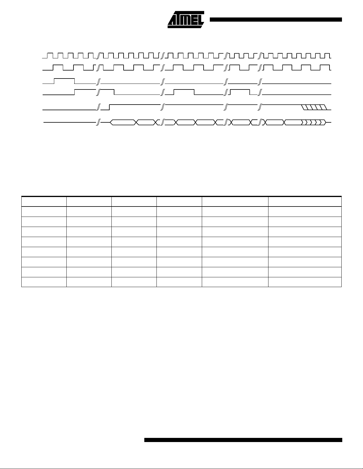
Figure 8. Serial bus timing
CLK
CLKR
ACK
FSR
CS
6 * 16 BITS
DATA
CH1, B15
MSB
CH1, B14 CH1, B0
LSB
CH2, B15
MSB
CH2, B0
LSB
CH6, B1 CH6, B0
Operating Modes of AT73C500
The AT73C500 chips et has six operating modes. The
mode is selected by three mode control inputs which
AT73C500 reads through a bus during the initialization procedure after a reset state. The operation of
AT73C501/AT73C502 is independent of the mode
selected.
Mode Number Mode Bit 2 Mode Bit 1 Mode Bit 0 Operating Mode Calibration Data Storage
0000Not in use
In operating mode 7, the default display pul se rate is 10
impulses per kWh, instead of 100 impulses per kWh, as in
other modes.
1001Normal operationEEPROM
2010Multi-channel operationEEPROM
3011Normal operationMicro-processor
4100Multi-channel operationMicro-processor
5101Test mode None
6110Not in use
7111Normal operationEEPROM
Normal Measurement Mode
AT73C500 devices support both stand-alone and microprocessor configurati on. The calib ratio n coeffi cient s ca n either
be supplied by a processor or stored in an 128 x 8-bit
EEPROM. The ROM is interfaced with AT73C500 via three
pin serial bus. AT73C500 and the processor communicate
through an 8-bit bus.
The only operational difference be tween stand-al one and
µP mode is the way of reading calibration co effi ci en ts. Th is
allows variou s combi nati ons of t hese tw o conf igurat ions t o
be utilized. For example, th e calib ration data can be sto red
in an EEPROM even though the processor reads and displays the measurement results supplied by AT73C500
device.
In most cases, the use of external EEPROM gives flexibility
to the meter testing and calibratio n, and also makes the
processor inte rface easier to implement. T herefore, th is
configuration is recommended even in meters equipped
with a separate microprocessor.
The same sequence of basic ca lculations is performed
both in poly-phase and single-phase meters. This
sequence consists of DC offset suppression, phase, gain
and offset c alibr atio n, c alc ula tions of mea surem en t qu antities and data transfer to µP bus and pulse outputs.
AT73C500 constantl y m oni tors v ario us ta mpe ring an d faul t
situations, which are indicated by status bits.
After a reset state, AT73C500 goes through an initialization
sequence. The device reads the operating mode and
fetches the calibration coefficients an d adjustment factors
for output pulse rate and starting current level, either from a
non-volatile memory or from a microprocessor. After that
the normal measurement starts. The reset state is normally
activated by power-up reset following the r ecovery from a
voltage interruption.
8
AT73C500
Page 9
AT73C500
Measurements and Calculations
The first operation performed by AT73C500 is digital highpass filtering. The purpose of the filtering is to remove the
DC offset of both current and voltage samples.
From offset free samples, active power is calcul ated
phase-by-phase with simple multiplication and additio n
operations.
First, the current samples are multiplied by voltage samples. The multiplic ation resu lts are summed ov er one lin e
period and finally the sum value is divided by 64. This discrete time operati on gi ve s the av erag e power of one 50 Hz
period and the result corresponds to the following continuous time formula:
T
N
1
P
=
---
ANUNsin n wt×{}ANINsin n wt ∅+×
×
∑
n0=
∫
T
0
N
1
=
-- -
A
∑
n0=
nAnUnIn
2
{}dt×××××[]
cos ∅
()×××××
N
n
where
T = 1/50 Hz,
n = 1, 2, 3,..., 20 (bas ic 50 Hz frequenc y and the har-
monics),
= frequency response of calculations.
A
n
This method of calculation does take into account the effect
of harmonics.
The total power is calculated by summing the power of
each line phase. Reactive power calculation is based on a
similar procedure. Before multipl ying the curr ent and voltage samples AT73C500 performs a frequency independent
90 degree phase sh ift o f the voltage signal. This is re a lize d
with a digit al H ilb ert t ran sform ati on f ilt er. T he ban dwidth of
reactive power measuremen t is limited to 360 Hz.
Based on the active and reactive results apparent power
and power factors ar e determined. RMS phase voltages
are calculated by squaring and summing the voltage samples and fina lly ta king a s quare r oot of the re sults . Cur rent
is determined by divi ding apparent po wer result by corr esponding phase voltage.
Frequency measurement is based on a comparison of the
line frequency and AT73C500 sampling clock frequency.
The measurement range is from 20 Hz to 350 Hz.
All measurements and calculations, except frequency measurement, are mad e over 1 0 l ine cy c le perio ds . T he re su lts
are updated and transferred to processor bus once in 200
ms.
Measurement Registers
For the measurement parameters 25 registers are allocated:
Register Meaning
REG0 Phase 1, active power, P1(10T), 32-bit register;
REG1 Phase 2, active power, P2(10T), 32-bit register;
REG2 Phase 3, active power, P3(10T), 32-bit register;
REG3 Phase 1, reactive power, Q1(10T), 32-bit regi ste r;
REG4 Phase 2, reactive power, Q2(10T), 32-bit regi ste r;
REG5 Phase 3, reactive power, Q3(10T), 32-bit regi ste r;
REG6 Phase 1, apparent power, S1(10T), 16-bit register;
REG7 Phase 2, apparent power, S2(10T), 16-bit register;
REG8 Phase 3, apparent power, S3(10T), 16-bit register;
REG9 Phase 1, power factor, PF1, 16-bit register;
REG10 Phase 2, power factor, PF2, 16-bit register;
REG11 Phase 3, power factor, PF3, 16-bit register;
REG12
REG13
REG14
REG15
REG16
REG17 Frequency, f, 16-bit regi ste r;
REG18 Reserved for further use, 16-bit register;
REG19 Phase 1, voltage U1, 16-bit register;
REG20 Phase 2, voltage U2, 16-bit register;
REG21 Phase 3, voltage U3, 16-bit register;
REG22 Phase 1, current I1, 16-bit register;
REG23 Phase 2, current I2, 16-bit register;
REG24 Phase 3, current I3, 16-bit register.
Active exported energy since the latest rese t, +Wp,
32-bit counter;
Active imported energy sin ce the latest rese t, -Wp,
32-bit counter;
Reactive energy, inductive load, Wqind, 32-bit
counter;
Reactive energy, capacitive load, Wqcap, 32-bit
counter;
Number of 10T periods elapsed since the latest
reset, 32-bit counter;
The size of the registers is either 16-bit or 32-bit. IEC specifications apply to the calculations of active and reactive
power and energy (REG 0-5 and REG 12-15). Other results
are intended mainly for demand recording and for va rious
diagnostic and display functions. The accuracy of those are
limited due to the finite resolution.
9
Page 10

In multi-chan nel mode the ac tive energy of each three
meters (phases ) is stored in regist ers 12-14 . REG15 i s not
in use.
The maximum value of different power registers differs,
depending on the calculation formulas used. The scaling of
registers is described below.
If a full scale sine signal is applied to voltage and current
inputs and the voltage and current channels are exactly in
the same phase, a value of 258F C2F7H will be produced
in the 32-bit P1, P2 and P 3 regist ers. The LS bit wi ll correspond to about 34 microwatts in nominal input conditions of
270V maximum phase voltage and 80A maximum current.
If the load is fully reactiv e (
scale signals are applied, the Q1, Q2 and Q3 register content will be 2231 594DH positive or negative, and the LSB
will represent about 38 µVAr. The maximum value of the
16-bit S registers is 258EH and this val ue is obtained if a
full scale amplitude is produced to the current and voltage
inputs. LS bit of the S registers correspond to about 2.25VA
power.
The following formula is used to calculate the power factor:
PF sign Q
The PF register contents 7FFFH represents power factor
value one and the contents 0000H value zero. Negative PF
values are stored corres pondi ngly a s nega tive b inary nu mbers. It should b e note d that the s ign of pow er fact or res ult
indicates whether the loading is inductive (+) or capacitive
(-).
The contents of fr equ enc y r egi st er ( REG 1 7) actually represents a 16-bit fi gure whi ch corresp onds to the du ration o f
50 line frequency cycles. The measurement is made by
comparing the line frequency with one of the sampling
clocks of AT73C500 and therefore the result depends on
the crystal frequency used. With default 3.2768 MHz crystal, the resolution of time value is 1.25 ms . To get the frequency, the following calculation has to be made:
If the master clock frequency (MCLK) of AT73C500 is not
nominal, the following formula gives frequency results:
40000
-------------------
f
REG17
± 90° phase differenc e) and full
abs P()
------------------
()
×=
abs S()
40000
-------------------
f
REG17
Hz=
MCLK
------------------------------
× Hz=
3.2768MHz
In the default condition, value 7FFFH of register 17 corresponds to 1.22 Hz frequency, value 0320H represents
50 Hz and 0001H 40 kHz. However, in practice, the bandwidth of frequency measurement is limited to 20 Hz to
350 Hz.
The frequency measurement is locked with one of the
phase voltages. If th is volt age disa ppears, AT7 3C500 tries
to track one of the other phases. The frequency measurement works down to about 10% level of the full scale voltage range. The harmonics content of phase voltage should
be below 10%. If it is hi gher, err oneous fre quency results
may be obtained.
The voltage registers (REG19-REG 21) are scaled so that
full scale sinusoidal input signal at AT73C501/AT73C502
voltage channels will produce 7A 8BH value into vo ltage
registers. This means that the resolution of the registers is
about 8.6 mV. Accordingly, full scale current will produce
7DA4H to current registers (REG22-REG24) pr oviding a
resolution of about 2.5 mA. In practice, the voltage can be
measured down to about 25V leve l and current down to
about 100mA.
If either voltage or current, or both, contain a considerable
amount of harmonics pr oducing a squ are wave type waveform, it is recommended to scale the input range so that the
maximum peak-to-peak v alue i s at l east 1 0% below the full
scale range of inputs. This is to avoid overflow in the calculations performed by AT73 C500 .
Energy Counters
Four 32-bit counters (REG12-REG15 ) measure energy
consumption. In nominal situations, the counters are
always increm ented wh en 0.4W h (0.4VA rh) energ y is consumed. The counters can store minimum of 1100 days consumption, provided that AT73C501/AT73C502 and
AT73C500 are used with default settings.
Impulse outputs are generated from these counters. The
meter constant rate represents 2 LSBs of a counter which
equals 0.8 Wh (0.8 VArh) and produces 1250
impulses/kWh. (1250 impulses/kVArh). In modes 1 to 4, the
display pulses are generated from 25 LSBs of a counter.
This corresponds to an impulse rate of 100 impulses/kWh
(100 impulses/kVArh). It is possible to adjust this rate with
MCC calibration c oefficient. In mode 7, 2 50 LSBs o f the
energy register is needed to gene rate one impu lse (10
impulses/kWh).
The default values above are based on 80A
current, 270V
rate.
The crystal frequency will affect the va lue s o f en er gy r egisters (REG12-REG15) and time register (REG 16). It will
also change the pulse rates of the impulse outputs.
full scale voltage and 3.2768 MHz clock
RMS
full scale
RMS
10
AT73C500
Page 11

AT73C500
It is recommended that 50 Hz mete rs are oper ated from
3.2768 MHz crystal. In 60 Hz system, a 3.93216 MHz clock
is normally used. Because the clock frequency generates a
time reference for energy c alculations, the content o f
energy registers and als o the puls e rate of impuls e outputs
will change when crys tal is changed. For ex ample, the
nominal meter constant and display pulse rate of 60 Hz
meter (3.93216 MHz clock) is:
60Hz
------------- -
==
MC
× 1500
50Hz
1250
imp
----------- -
kWh
imp
----------- -
kWh
and
×
100
imp
----------- -
kWh
DP
REG0 - REG2 U = 270V, I = 80A, PF = 1 258F C2F7 34.276 µW
REG3 - REG5 U = 270V, I = 80A, PF = 0 2231 594D 37.653 µVAr
REG6 - REG8 U = 270V, I = 80A 258E 2.2467 VA
REG9 - REG11
50Hz
Register Conditions Full Scale Output (hex) Resolution (hex)
60Hz
------------- -
==
120
imp
----------- -
kWh
PF = 1
PF = -1
The LSB of energy registers corr espond to 0.33Wh instead
of 0.4Wh, as follows:
E
LSB
--------------------------------- -
3.93216MHz
× 0.333333…Wh==
0.4Wh
3.2768MHz
The pulse rate can be scaled to 100 imp/kWh by programming value 5 to MCC coefficient, as below:
1
IMP (25 MCC)
===
---------
E
×+ 30
imp
LSB
1
---------
0.3333…Wh× 10
imp
Wh
-------- -
imp
which equals 100 impulses per kilowatt hour.
The following table sum marizes the co ntents of all m ea-
surement registers.
7FFF
8001
0.0000305
-0.0000305
REG12 - REG15 W = 1.718GWh FFFF FFFF 0.4Wh
REG16
REG17 50*T = 40.959s 7FFF 1.25 ms
REG19 - 21 U = 270V 7A8B 8.6 mV
REG22 - 24 I = 80A 7DA4 2.5 mA
∆T = 238609.3h FFFF FFFF 0.2s
11
Page 12

Output Operations
The data output by AT73 C500 can be divided in to three
categories: d ata to external proces sor, s tatus inform ation
and impulse outputs. AT73C500 reads mode informa tion,
and in mode 3 and 4, also calibration data via external bus.
For the I/O operation, two 8-bit buses are allocated.
The same eig ht data lines are reserved both for the
impulse outputs and for the proc essor in terface. The se paration is done with two a ddr ess pi ns . W hen comm uni ca tin g
with the microprocess or, address 1 (pin A DDR1) is ac tivated (high). Impulses are output combined with a high
level of address 0 (A DDR0). For status information separate 8-bit bus is reserved. The table below describes the
use of the two buses of AT73C500.
Data bits Bus Address Mode Usage
B0 - B7 Data Bus ADDR0 Output
B8 - B15 Status Bus ADDR0 Output
B0 - B7 Data Bus ADDR1
B12 - B14 Status Bus ADDRx Input
Input/
Output
Impulse
Outputs
Status
Information
Processor
Interface
Mode
Inputs
For status and impulse outp uts, external latches are
needed to store the information while buses are used for
other tasks. In most case s, the data bus of AT73C5 00 and
processor I/O bus c an be connecte d directly with e ach
other. The data transfer is controlled by handshake signals,
ADDR1, RD/WR, STROBE and BRDY. One of the status
outputs DATRDY (B9, ADDR0) can be used as an interrupt
signal. Interrupt can be also generated from the handshake
lines.
In most meters, only some of the I/O operations of
AT73C500 are needed. If a meter con tains a separate processor, status outputs of AT73C500 are typically not used
since the processor will anyway track the status information
supplied by AT73C50 0. Often only one or two o f the
impulse outputs are wired to the test LED or electromechanical counter.
Data Transfer to External Microprocessor
The calculation results of AT73C500 are transferred to processor via 8-bit parallel bus. During norma l operation, the
information transfer is divided into six packages which are
written in 200ms intervals after the calculations over ten
line frequency cycles have been completed. There is a time
interval of one line cycle between each individual dat a
package. The first four bytes of a package contain synchronization, mode and status infor mation, and th e rest 12
bytes are reserved for the actual measurement results. The
contents of the six data packages are as follows:
Table 1. Package 0
Byte Data Order Meaning
1 Sync LS Single byte Synchronization
2 Sync MS Single byte Synchronization
3 Mode Single byte Mode information
4 Status Single byte Status information
5 REG0 (LS+2) byte Active power, phase 1
6 REG0 MS byte Active power, phase 1
7 REG0 LS byte Active power, phase 1
8 REG0 (LS+1) byte Active power, phase 1
9 REG1 (LS+2) byte Active power, phase 2
10 REG1 MS byte Active power, phase 2
11 REG1 LS byte Active power, phase 2
12 REG1 (LS+1) byte Active power, phase 2
13 REG2 (LS+2) byte Active power, phase 3
14 REG2 MS byte Active power, phase 3
15 REG2 LS byte Active power, phase 3
16 REG2 (LS+1) byte Active power, phase 3
12
AT73C500
Page 13

AT73C500
Table 2. Package 1
Byte Data Order Meaning
1 Sync LS Single byte Synchronization
2 Sync MS Single byte Synchronization
3 Mode Single byte Mode information
4 Status Single byte Status information
5 REG3 (LS+2) byte Reactive power, phase 1
6 REG3 MS byte Reactive power, phase 1
7 REG3 LS byte Reactive power, phase 1
8 REG3 (LS+1) byte Reactive power, phase 1
9 REG4 (LS+2) byte Reactive power, phase 2
10 REG4 MS byte Reactive power, phase 2
11 REG4 LS byte Reactive power, phase 2
12 REG4 (LS+1) byte Reactive power, phase 2
13 REG5 (LS+2) byte Reactive power, phase 3
14 REG5 MS byte Reactive power, phase 3
15 REG5 LS byte Reactive power, phase 3
16 REG5 (LS+1) byte Reactive power, phase 3
Table 3. Package 2
Byte Data Order Meaning
1 Sync LS Single byte Synchronization
Table 4. Package 3
Byte Data Order Meaning
1 Sync LS Single byte Synchronization
2 Sync MS Single byte Synchronization
3 Mode Single byte Mode information
4 Status Single byte Status information
5 REG12 (LS+2) byte Active exported energy
6 REG12 MS byte Active exported energy
7 REG12 LS byte Active exported energy
8 REG12 (LS+1) byte Active exported energy
9 REG13 (LS+2) byte Active imported energy
10 REG13 MS byte Active imported energy
11 REG13 LS byte Active imported energy
12 REG13 (LS+1) byte Active imported energy
13 REG14 (LS+2) byte
14 REG14 MS byte
15 REG14 LS byte
16 REG14 (LS+1) byte
Reactive energy,
inductive load
Reactive energy,
inductive load
Reactive energy,
inductive load
Reactive energy,
inductive load
2 Sync MS Single byte Synchronization
3 Mode Single byte Mode information
4 Status Single byte Status information
5 REG6 LS byte Apparent power, phase 1
6 REG6 MS byte Apparent power, phase 1
7 REG7 LS byte Apparent power, phase 2
8 REG7 MS byte Apparent power, phase 2
9 REG8 LS byte Apparent power, phase 3
10 REG8 MS byte Apparent power, phase 3
11 REG9 LS byte Power factor, phase 1
12 REG9 MS byte Power factor, phase 1
13 REG10 LS byte Power factor, phase 2
14 REG10 MS byte Power factor, phase 2
15 REG11 LS byte Power factor, phase 3
16 REG11 MS byte Power factor, phase 3
13
Page 14

Table 5. Package 4
Table 6. Package 5
Byte Data Order Meaning
1 Sync LS Single byte Synchronization
2 Sync MS Single byte Synchronization
3 Mode Single byte Mode information
4 Status Single byte Status information
5 REG15 (LS+2) byte
6 REG15 MS byte
7 REG15 LS byte
8 REG15 (LS+1) byte
9 REG16 (LS+2) byte Counter
10 REG16 MS byte Counter
11 REG16 LS byte Counter
12 REG16 (LS+1) byte Counter
13 REG17 LS byte Frequency
14 REG17 MS byte Frequency
15 REG18 LS byte Reserved
Reactive energy,
capacitive load
Reactive energy,
capacitive load
Reactive energy,
capacitive load
Reactive energy,
capacitive load
Byte Data Order Meaning
1 Sync LS Single byte Synchronization
2 Sync MS Single byte Synchronizat ion
3 Mode Single byte Mode information
4 Status Single byte Status information
5 REG19 LS byte Voltage, phase 1
6 REG19 MS byte Voltage, phase 1
7 REG20 LS byte Voltage, phase 2
8 REG20 MS byte Voltage, phase 2
9 REG21 LS byte Voltage, phase 3
10 REG21 MS byte Voltage, phase 3
11 REG22 LS byte Current, phase 1
12 REG22 MS byte Current, phase 1
13 REG23 LS byte Cu rrent, phase 2
14 REG23 MS byte Current, phase 2
15 REG24 LS byte Cu rrent, phase 3
16 REG24 MS byte Current, phase 3
The six data packages arrive as follows:
16 REG18 MS byte Reserved
Figure 9. Data transfer to processor in six packages
20 ms
200ms = 655360 clocks @ 3.2768 MHz
Pack0Pack1Pack2Pack
3
DATRDY
LINE PERIOD
1234567891012345
In normal mode, the Sync LS byte indicates the number of
data package which wi ll follo w (value 0...5) . There are als o
two special situations indicated by this byte. Value six of
Sync LS byte means that the processor is expected to supply calibration data to AT73C500. Value seven is written by
Pack4Pack5Pack0Pack1Pack2Pack
3
AT73C500 in case power interruption is detected and billing information needs to be transferred to microprocessor.
In this case the proc essor knows that both packa ges 3 an d
4 will follow one after each other as shown in Figure 10.
14
AT73C500
Page 15

AT73C500
Content of Sync LS byte i s des cr ibed in the following table .
Bits 3-7 of the Sync LS byte are not used.
Table 7. Sync LS Byte
Data
B7 - B3 B2 B1 B0
X X X X X 0 0 0 0
X X X X X 0 0 1 1
X X X X X 0 1 0 2
X X X X X 0 1 1 3
X X X X X 1 0 0 4
X X X X X 1 0 1 5
X X X X X 1 1 0 (none)
X X X X X 1 1 1 3 and 4
package Mode
Normal operation,
Data output
Normal operation,
Data output
Normal operation,
Data output
Normal operation,
Data output
Normal operation,
Data output
Normal operation,
Data output
DSP waiting for
calibration data
PFAIL active,
billing information
to be transferred
The Sync MS byte contains a unique 8-bit data, 80H. It can
be used as a synchronization byte by the external controller.
The mode byte contains the following information:
Figure 10. Meaning of bits in mode byte
Mode byte
Not used State of MODE
input pins of the
B0B1B2B3B4B5B6B7
DSP
The contents of the status byte equals the content of the
external Status bus as described in the section “Status
Information” on page 17.
In the beginning of I/O operation, AT73C500 writes a high
pulse to B9 pin of the Status bus (ADDR0). This pin can be
externally latched to lengthen the pulse over the whole output operation. It can be used to generate a da ta ready
(DATRDY) interrupt to processor.
Figure 11 shows the timing of one data package. In nominal conditions, it takes 200 clock cycles to transfer all 16
bytes. A high pulse (DATRDY) is written to bit B9
(SMBUS1) of Status bus 11 clo cks before t he firs t byte is
available and low pulse 12 c locks after the last byte has
been sent.
15
Page 16

Figure 11. Contents of a data package
45 clock cycles 143 clock cycles
LATCHED
DATRDY
CLK
STROBE
200 clock cycles
Sync LS Sync MS Mode Status Data 1 Data 2 Data 11
Synchronisation data Status data
AT73C500 offers some time for the processor to analyze
the synchronization, status and mode information before
starting to supply the measurement results. The 12 measurement bytes are written on every 11th clock period.
Four handshake signals are provided, ADDR1, RD/WR,
STROBE and BRDY, for interfacing with the microprocessor. ADDR1 is always taken high when AT73C500 is either
Figure 12. Handshake signals of the DSP
CLK
SDLY
DATA
FROM DSP
DDLY
BRDY
SH
STROBE
Measurement data, 12 bytes
Data 12
writing to µP bus or reading the bus contents. When used
with slow peripheral, the BRDY input of AT73C500 can be
used to hold the device in write mode until the processor
has finished reading the bus. However, the total length of
one data package should always be less than 300 clock
cycles of AT73C500. Longer I/O periods may result erroneous measurement results.
BRS
ASU
ADDR1
RWSU
RD/WR
RWH
Following the falling edge of BRDY, the data ca n be
strobed into the µP by th e risi ng edge of the ST ROBE s ignal. If the microprocessor is able to read data continuously,
BRDY can be kept constantly low. Also BRDY should be
low whenever DATRD Y is inactive allo wing AT73C500
freely use its buses.
16
AT73C500
To avoid conflicts, the processor shou ld always k eep its
bus in tri-state mod e, unless it is us ed to write cali bration
coefficients to AT73C500.
Page 17

AT73C500
Status Information
AT73C500 provides the following status information
through the Status bus of AT73C500 (B8 - B15, ADDR0).
Status
Bus Bit
B15 TAMP
B14 STUP
B13 L3
B12 L2
B11 L1
B10 FAIL High: Operating error detected
B9 DATRDY High: Data available on the µP bus
B8 INI
Status
Flag Meaning
High: Potential event of
tampering detected
High: Current of all phases
below starting level
High: Phase 1 voltage above
10% of full-scale
High: Phase 2 voltage above
10% of full-scale
High: Phase 3 voltage above
10% of full-scale
Low: AT73C500 in initialization
phase, EEPROM interface in use,
AT73C501 (or AT73C502) interface
disabled
High level of Lx fl ags indicate s that a phase volta ge is
above 10% level of the full scale voltage. If a voltage drop
is detected, the corresp onding status bit is writte n low.
AT73C500 is continuousl y monitoring the vo ltage of each
phase.
FAIL flag signifies that som ething abnormal has been
detected. The following situations may cause a high level of
FAIL: read operation of cali bration coeffic ients is not su ccessful, the serial bus of A T73C501 or AT73C5 02 is not
working properly, the measurement results can’t be transferred to microprocessor, AT73C500 has detected an internal failure.
If any of the calibration coefficients and co rresponding
back-up values do n ot match, AT73C500 performs two
extra read operations to eli minat e the po ssib ility of a tran sfer error. If the error still exists after the third trial, incorrect
coefficients are replaced by the default values. FAIL flag is
activated in dicating that a potent ial error has been
detected. FAIL is also taken high in case it is not possible
to read calibration c oeffic ients fr om the µP or EE PROM , or
if the processor supplies too few coefficients. In both cases,
the read operation will finish in a time-out situation.
The voltage monitoring block of AT73C501/AT73C502 is
used to detect voltage interruptions before the supply voltage of AT73C500 drops. High level of PFAIL output at the
ADC indicates a voltage break situation. The measurement
results supplied by AT73C501/AT73C502 may be erroneous, and AT73C500 and microprocessor has to be prepared for supply volta ge interr uption. A hig h level of PF AIL
causes an immediate write of data packages 3 and 4
(accumulated energy information) to processor bus. The
timing of t h is op er at i on i s pr es en t e d i n F i g ure 1 3. Th e re ar e
16 clocks between the two 12 byte data packages but the
header bytes are no t repeated in the beginni ng of pa ckag e
4.
Figure 13. Transfer of billing information to processor following a PFAIL interrupt
337 clock cycles
45 clock cycles 280 clock cycles
LATCHED
DATDRY
CLK
STROBE
Sync LS Sync MS Mode Status Data 1 Data 2 Data 12
Synchronisation data Status data
In case of an imminent voltage break, the microproces sor
stores the energy val ues into a non- volatile memory. The
devices can operate for a short period of time powered by
an electrolytic capacitor or by battery back-up.
AT73C500 dev ices ar e taken to a soft reset st ate a nd normal operation will be recovered after the supply voltage is
high again. About one line cycle is needed to start normal
measurements. During this initialization phase no calculations are performed.
STUP output (active high) indicates that the current of each
of the three phases is below the specified starting level and
no energy is accumulated. This status flag is very useful
during the calibration of a meter si nce immediate feedback
about staring current level is provided.
TAMP flag informs about potential tampering. It is activated
if one or more phase currents are zero or negative. Therefore it very effectively indicates current transformer reversal
or short-circuit.
Measurement data, 12 bytes + 12 bytes
Data 1
Data 12Data 2
17
Page 18

Impulse Outputs
AT73C500 provid es eigh t imp ulse outpu ts, fo ur m eter c onstant outputs an d four pulse ou tputs to drive el ectromechanical display counters which can register exported and
imported active energy and capacitive and inductive reactive energy. These outputs use the same output lines as
used for the processor interface. Impulses are combined
with address 0 (ADDR0). The table below shows the
impulse outputs avail able in mo des 1 and 3 . Mode 7 offe rs
the same outputs, but the rate of the display pulses is
10imp/kWh (kVArh).
Table 8. Impulse Outputs in Operating Modes 1 and 3
Output Bit Impulse Output Type Impulse Rate
B7 - VArh Meter Constant 1250imp/kVArh
B6 + VArh Me ter Co nst ant 1250imp/kVArh
B5 - Wh Meter Constant 1250imp/kWh
B4 + Wh Meter Constant 1250imp/kWh
B3 + Wh Display 100imp/kWh
B2 - Wh Display 100imp/kWh
B1 + VArh Disp lay 100imp/kVArh
B0 - VArh Display 100imp/kVArh
An external regis ter is needed to latch and buf fer the
pulses. The regis ter can further driv e both elec tromec hanical display cou nter s and LED s. In mo des 1 to 4, the no minal pulse rate of display outputs is 100imp/kWh or
100imp/kVArh (U
MAX
= 270V, I
= 80A) and meter con-
MAX
stant outputs 1250imp/kWh (1250imp/kVArh). The length
of each display pulse is 117ms when operated from
3.2678 MHz crystal. Me ter c ons ta nt p uls e sta ys h igh for 2 0
ms.
If the devices are used in a 5A mete r, cu r re nt in put s ca n be
scaled to 8A full scale level. In this case, the nominal
impulse rates are ten times higher than the above values.
Multi-channel Mode
Modes 2 and 4 are reser v ed fo r mul ti- chan nel op er ati on. I n
these modes, the chip s oper ate like thr ee ind ependen t single phase meters and stor e the calculati on resul ts in separate registers ph ase-by -phase (m eter-by -meter ). Th e bas ic
sequence of operation is otherwise similar to the normal
mode.
Impulse Outputs
In multichannel operation three impulse outputs ar e available for display counters. The absolute energy value is
measured and the rever sal of curr ent flow doe sn’t affe ct t o
pulse rates. Th e FAIL signal can, however, be used to
determine whether the energy being registered is pos itive
or negative. Met er co nstan t pul se rat e co rresp onds to to tal
active energy of the three single phase channels summed
together as shown in the table below.
Output Bit Impulse Output Type Impulse Rate
B7 Not Used Not Used B6 Not Used Not Used B5 Not Used Not Used -
Meter Constant
B4 ± Wh
B3 ± Wh
B2 ± Wh
B1 ± Wh
B0 Not Used Not Used -
Sum of all 3
channels
Display,
Channel 1
Display,
Channel 3
Display,
Channel 2
1250imp/kWh
100imp/kWh
100imp/kWh
100imp/kVArh
Test Mode
This mode can be used for initi al calibrati on purpose s or in
a special meter for additional processing of sample data. In
this mode, AT73C501/AT73C502 sa mples the six inputs
normally and transfers the samples to AT73C500, which
performs DC suppression and further writes the samples to
8-bit processor bus together with header bytes in the following sequence.
Byte Contents
1 Sync LS byte
2 Sync MS byte
3 Mode Byte
4 Status Byte
5,6 I1, LS byte and MS byte
7,8 U1, LS byte and MS byte
9,10 I2, LS byte and MS byte
11,12 U2, LS byte and MS byte
13,14 I3, LS byte and MS byte
15,16 U3, LS byte and MS byte
Several input combinations can be measured to check the
gain and phase error in different conditions. An interfacing
computer can be programmed to calculate the calibration
coefficients based on the samples supplied by AT73C500.
At the end of the cali bration, the coef ficients have to be
stored in a non-volatile memory of the meter as described
in “Loading of Calibration Coefficients” on page 19.
18
AT73C500
Page 19

Calibration
The calibration coefficien ts always hav e to be loaded into
AT73C500 registers after reset state. The coefficients are
either read from an external EEPROM or supplied by a
microprocessor via the 8-bit bus.
Loading of Calibration Coefficients
In modes 3 and 4, a microprocessor takes care that the
coefficients are kep t in a non- volatile m emory during voltage break. After the voltag e break, the DSP first write s the
Figure 14. Timing of calibration coefficient read operation
CLK
AT73C500
four header bytes, Sync LS, Sync MS, mode and status
information on the µP bus and then starts waiting for the
calibration data. The processor reads the status and mode
and after that writes the coeffi cients on the bus. T he contents of AT73C500 header bytes is described in “Data
Transfer to External Microproc essor” on page 12 and “Sta-
tus Information” on page 17.
DATRDY
STROBE
SYNC LS SYNC MS MODE STATUS COEFFICIENT 0
HEADER DATA SUPPLIED BY AT73C500 44 COEFFEICIENTS READ
Before using the µP bus, AT73C500 writes a short pulse
(DATRDY) to B9 bit of the Status bus combined with hi gh
level of address 0 (ADDR0 output). This bit can be taken
directly or through an e xternal latch to the inte rrupt in put of
the processor. After writing the status and mode bytes,
AT73C500 goes to a read mo de and star ts waiti ng for calibration coefficients from the µP. Processor supplies the
coefficients as 8-bit bytes one after another. The timing of
this sequence is presented in Figure 14.
AT73C500 READY TO
READ CALIBRATION DATA
. . .
COEFFICIENT 1
COEFFICIENT 42
COEFFICIENT 43
Nine gain calibration, six offs et calibrati on and three phase
calibration coeffi cients are read into the AT7 3C500 memory. At the same time, a scalin g fact or for the disp lay pu lse
rate and an adjustment va lue for starting current is stored.
To minimize the risk of erroneous calibr ation values, a
back-up valu e of each co effici ent i s a lso tr ans ferred by the
microprocessor or from the ROM. The back-up value has to
be written as 2’s complement binary number of the actual
calibration figure.
19
Page 20

The calibration data is transferred in the following sequence:
Byte Calibration Coefficient Byte Calibration Coefficient
0 PC1 1 PC1 back-up
2 PC2 3 PC2 back-up
4 PC3 5 PC3 back-up
6 MCC 7 MCC back-up
8 Not used 9 Not used
10 AGC1 11 AGC1 back-up
12 AGC2 13 AGC2 back-up
14 AGC3 15 AGC3 back -up
16 RGC1 17 RGC1 back-up
18 RGC2 19 RGC2 back-up
20 RGC3 21 RGC3 back-up
22 UGC1 23 UGC1 back-up
24 UGC2 25 UGC2 back-up
26 UGC3 27 UGC3 back-up
28 STUPC 29 STUPC back-up
30 AOF1 31 AOF1 back-up
32 AOF2 33 AOF2 back-up
34 AOF3 35 AOF3 back-up
36 ROF1 37 ROF1 back-up
38 ROF2 39 ROF2 back-up
40 ROF3 41 ROF3 back-up
42 OFFMOD 43 OFFMOD back-up
The meaning of the calibration coefficient mnemonics are as follows:
Mnemonic Meaning
PC
N
MCC Display pulse adjustment factor for active and reactive energy
AGC
N
RGC
N
UGC
N
STUPC Starting current adjustment factor
AOF
N
ROF
N
OFFMOD Controls the use of offset factors
Phase calibration factor, phase N
Gain calibration factor f or active power and energy calculation, phase N
Gain calibration factor for reactive power and energy calculation, phase N
Gain calibration factor for phase voltage, phase N
Offset calibration factor for active power and energy calculation, phase N
Offset calibration factor for reactive power and energy calculation, phase N
20
AT73C500
Page 21

AT73C500
AT73C500 provides four handshaking signals, ADDR1,
RD/WR, STROBE and BRDY, for interfacing with the
microprocessor. Microprocessor can use the BRDY input of
AT73C500 to ext end th e r ead a nd wri te cy cles . AT73 C500
stays in the read or w rite mode a s long as B RDY is high .
BRDY is sampled at the rising edg e of AT73 C500 master
clock. As soon as BRDY goes low, the read/write cy cle of
AT73C500 will end a t the first rising ed ge of CLK clock .
During read operation data is latched into AT73C500 register on the rising edge of the STROB E signal following th e
low level of BRDY. A more detailed description about the
handshake signals is presented in sec tion “Data Transfer
to External Microprocessor” on page 12.
Fifteen idle cycles are inserted by AT73C500 between the
read operation of each calibration byte. This allows the processor to prepare the next coefficient for transfer or to raise
the BRDY signal in case it is not ready to write the following
byte. If the data is avail able, BRDY ca n be kep t consta ntly
low. Microprocess or ha s to always sup ply all 4 4 calib ratio n
bytes even though some of those may be zero and don't
affect to measurement results.
If AT73C500 detects an error when comparing the calibration data and corresponding back-up values, it writes the
DATRDY bit high and after that the header bytes on processor bus indicating that it is still in initialization routine
and wishes to get the calibration data to be transported
once again. If th e error still e xists after the t hird trial,
AT73C500 notifies the situation by a FAIL status bit and
starts normal operation, discarding potentially incorrect calibration coefficients.
If AT73C500 is programmed to mode 1 or 2, the coefficients are stored in an EEPROM of type AT93C46. The
ROM has to support comm unication throu gh a three pin
serial I/O port. Th e serial ROM inte rface uses the s ame
port, which also connects AT73C500 to
AT73C501/AT73C502 sample output. During the initialization phase, the ADC interfa ce has to be dis abled. This can
be done by B8 bit of AT73C500 Status bus (ADDR0). The
output has to be latc hed by an ex te rnal fli p- flop to keep the
state over the whole initialization period. The same output
can be used as Chip Select input for the EEPRO M.
AT73C500 reads, checks and stores automatically all 44
calibration c oefficien ts. After t hat, B8 bit of S tatus by te is
written low and normal measurement can start. If the
EEPROM contains er roneous data and on e or mor e coef ficients don’t match with thei r back -up va lue s, the sa me pr ocedure is followed as in the processor mode .
Gain Calibration
Gain calibration is used to compensate the accumulated
magnitude error of voltage dividers, current transformers
and A/D converters. There is a separat e 8-bit gain calibration coefficient for each phase, and for active and reactive
energy measurem en t. A si milar formula is also u se d to ca l-
ibrate the phase voltage values, only the calibration range
is different, 20% for power and 8% for voltage. These calibrations will automatically cor rect the gain error of other
measurement parameters.
The following calculations are done to get the calibrated
results. For active power:
AGC
P
=
P
N
10.2
×
N
where PN is the active power of phase N and AGC
----------------
×+
128
N
is the
N
gain calibration facto r of that phase. The vali d range for
AGC
is -128 to +127. Similarly, for reactive power:
N
RGC
Q
=
N
Q
10.2
×
N
×+
where QN is the reactive power of phase N and RGC
the gain calibration coefficient for that phase. RGC
---------------- -
128
N
is
N
valid
N
range is -128 to +127.
Gain calibration performed on voltage measurements are:
UGC
U
=
U
N
10.08
×
N
×+
where UN is the line voltage of phase N and UGC
---------------- -
128
N
is the
N
corresponding gain calibration coefficient, ranging from
-128 to +127.
Apparent power and c urrent are automatically gai n
adjusted to match the ca librated se ttings of active po wer,
reactive power and voltage.
Offset Calibration
The low current response of current sensors is often more
or less non-linear. The error caused by this non-linearity
can be compensated by a small of fset factor which is
added in power results. Offs et cali bration i s done for active
and reactive power, se parately for each p hase. T he foll owing formulas are used:
AOF
N
P
NPN
--------------- -
128
0.004157 sign
×× (P
)P
×+≡
N
FS
and
ROF
N
Q
N
where P
and QN are the active and reactive power for
N
phase N, AOF
--------------- -
Q
N
128
and ROFN are the respective offset calibra-
N
tion coefficients and P
0.00457 sign(Q
and QFS are the corresponding full
FS
×× )Q
×+=
N
FS
21
Page 22

scale values of the powers. The nomi nal full-scal e values
are:
current. The chipset has a preprogra mmed startin g curre nt
level of
P
Q
270V 80A× 21.6kW==
FS
270V 80A× 21.6VAr==
FS
The valid range for the offset cali bration facto rs is -128 to
+127.
The scale of offset calibration for active and reactive power
is different, 89W versus 98VAr in nominal conditions of
270V maximum phase voltage and 80A maximum phase
current. Typically, a small offset factor of a few watts is
enough to compensa te the non-l ine ar ity of cu rre nt se ns ing .
It should be noted that offset calibration will also affect the
starting current level of a meter. If the full scale current or
voltage is changed to a non-default value, the range for offset calibration will be scaled accordingly.
The same offset value is used independent of phase angle.
However, as default (OFFMOD=0), the sign of power is
taken into accoun t in the c alc ula t io ns so that positive offse t
factor will always increase the absolute power value and
negative coefficient will decrease absolute results. This
guarantees that cur ren t se nsor non- linear ity is c orre cted in
the same way even though the current flow is reversed.
It is possible to ch ange this defaul t conditi on by progr amming value one to OFFMOD c oeffici ent. In th is cas e, offse t
coefficient will be always added to power result without
checking the sign of the power. Pos itive coefficient will
increase the abs olute value of positive po wer results and
decrease the absolute value of negative result.
Phase Calibration
The phase difference betwee n vol tag e and cur rent chan nel
is compensated with three 8-bi t phase calibrati on figures.
The displacement is usuall y due to the ph ase shift i n current transformers. Ba sed on the cali bration values, th e
DSP interpolates new current samples with sample instants
coinciding with the corresponding voltage samples. The following formula is used to determine the phase offset to be
used in the interpolation. One 8-bit phase calibration value
is stored for each of the three phases.
PC
N
----------- -
N
128
5.625
°×=
where PO
PO
is the sample phase offset of channel N, mea-
N
sured as phase(U) - phase (I). The allowed range for phase
calibration factor, PC
, is -128 to +127.
N
Starting Current Adjustment
The meter IC is designed to fulfill IEC 1036, class 1 specification. This specif ication is based on a certain basic current, I
. As a default, AT73C5 00 operates with 5A basic
b
1
------------ -
×=
I
FS
where I
I
SU
4000
is the full s cale current of the mete r, i.e. 80A i n
FS
nominal conditions. The defau lt startup current corresponds to 0.4% of the 5A I
, assuming that the full-scale
b
range is 80A. When the phase current is below the star ting
level, the calculated cycle power results are replaced by
zeros and no energy is accumulated.
It is possible to adjust the start-up level in the range of 0.2
to 10 compared with the nominal value. This is performed
with a special calibration factor. The following form ula is
used to determine the current:
SU
------------ -
4000
(1 0.2 STUPC)×+××=
I
FS
I
1
where STUPC is the sta rting current cali bration factor ,
allowed to vary in rang e -4 to +45, only. Care should b e
taken that the STUPC is correctly progr ammed and is not
beyond -4 to 45 range. Als o, it should be noted that lo w
starting thresholds may force the device to a level where
accuracy is restricted due to a finite resolution of converters
and mathematics.
Adjustment of Display Pulse Rate
An 8-bit byte is provid ed for adju stmen t of the i mpulse r ate
of display pulses. This coefficient will only affect the display
pulse rate of active and reactive energy but not to the meter
constant rate. The content of all measurement registers will
remain unchanged.
The impulse rate can be scale d in the r ange of 1 to 6 compared to the nominal value. In default conditions (U
270V, I
= 80A) the L SB of ener gy regi sters REG12-1 5
max
max
=
(See “S tatus Infor mation” on page 17.) corresponds to
0.4Wh. This means that accumulated 25 LSBs of energy
will generate one pulse to the displa y pulse output (25 x
0.4Wh/impulse = 10 Wh/impulse = 100 impulses/kWh).
By using MCC calibration coefficient, the nom inal figure 25
can be changed in the range of 25 to 152. MCC may range
from 0 to 127, only. The f oll owi ng f ormul as ar e used to calculate the impulse rate.
IMP (25 MCC) E
×+=
LSB
and
PR
--------------------------------------------------=
(25 MCC) E
1000
×+
LSB
22
AT73C500
Page 23

AT73C500
where ELSB is the energy value of one LSB in the energy
register, 0.4Wh i n default con ditions. When the m eter is
operated in non-standard conditions, the energy LSB may
be recalculated as:
U
3.2768MHz
E
LSB
------------------------------
f
where f is the clock frequency used, and U
×
FSIFS
------------------------------ -
270V 80A×
××=
0.4Wh
and IFS are
FS
the full-scale values of voltage and current.
In case the meter is used with a non- de faul t vo ltag e div ider
or current sensor, MC C factor is a con venient way to re adjust the impulse rate.
Example
The meter is to be configured for u se in 120V networks,
with a maximum line voltage o f 140V. The display puls e
rate is required to remain at 100imp/kWh. To start off, the
front end of the meter must be configured for the new line
voltage. The voltage dividers must be configured to produce an input signal of 0.707V at the input of the ADC at
maximum line voltage. At nominal meter settings, the voltage divider rati o is 270V:0.7 07V, in this case it must b e
140V:0.707V.
Note that adjus ting the l ine volta ge of the meter wil l rend er
the formatting of most calculation registers to alternative
settings. For example, the meter constant pulse rate will
change as follows:
MC
270V 80A
×
------------------------------ -
U
×
FSIFS
f
------------------------------
3.2768MHz
××=
1250
imp
----------- -
kWh
In our case of a meter for 120V netw orks, th e new me ter
constant pulse rate would be:
270V
------------- -
MC
==
× 2410.714…
140V
1250
imp
----------- -
kWh
imp
----------- -
kWh
To make the meter con sta nt pu lse r ate to a n ev en n umb er ,
for example 2500, we m ay choose to either re-scal e the
line voltage or scale the maximum line current. 2500
impulses per kilowatt hour is gained by either setting the
maximum line voltage to:
Regardless of which parameter (or both) is chosen, the
scaling process is a simple matter of gain ca librati on. If, for
example, the line voltage is chosen to be rescaled to 135V,
this is realized with a resistor divider of half the nominal,
and finetuning using the voltage gain coefficients. Also, all
values resulting from voltage calculation, such as the data
transferred via ener gy regi ster s, shoul d be nor mali zed wi th
respect to the new voltage setting.
Going back to the calibration of the display pulse rate, the
new LSB value of energy registers is:
140V
------------- -
× 0.20741…Wh==
E
LSB
270V
0.4Wh
To maintain the display puls e rate at 100 , the MCC c ali bration coefficient must be programmed as:
MCC
1000
----------------------------- - 25–
PR E
×
LSB
-------------------------------------------- --------------- 25– 23.216… 23≈== =
100
imp
----------- -
kWh
1000
×
0.20741Wh
The energy value of each disp lay c ounter i mpuls e is t hereafter:
IMP (25 23)
---------
imp
140V
------------- -
270V
0.4Wh 10.0
Wh
---------
≈××+=
imp
1
In mode 7, the default display pulse rate is 10
impulses/kWh(kVArh) instead of 100 impulses/kWh. This is
convenient for meters where only one decimal digit wants
to be shown. This default rate can also calibrated and the
calibration formulas are:
IMP (250 MCC) E
×+=
LSB
and
FS
-------------------------
U
2500
× 135V==
imp
----------- -
kWh
270V
1250
imp
----------- -
kWh
or by retaining the line voltage at 140V and scaling the
maximum line current to:
--------------------------------------------- -
I
FS
140V 2500
270V 80A×
×
× 77.143…A==
imp
----------- -
kWh
1250
imp
----------- -
kWh
PR
-----------------------------------------------------=
(250 MCC) E
1000
×+
LSB
Master Clock
The master clock of AT73C500 is generated by a crystal
oscillator with crystal connected between pins XI and XO of
AT73C501/AT73C5 02. M aster clock can also be f ed to the
XI input from a separate clock source. The system clock
rate of AT73C500 is the same as the clock of
AT73C501/AT73C502 and is fed to the CLK input of the
device from the CLK output of AT73C501/AT73C502.
23
Page 24

Electrical Characteristics
Absolute Maximum Ratings
Parameter Min Typ Max Unit
Supply Voltage V
V
, V
DA
DDA
Input Voltage, Digital
Input Voltage, Analog
Input Voltage, CI and
VI inputs
Ambient Operating
Temp.
Storage Temperature -65 +150 C
Calibration Characteristics
Parameter Min Typ Max Units
Gain Calibra tion
Calibration Range ± 20 %
Calibration
Resolution
Phase Calibration
Calibration Range ± 5.625 degree
Calibration
Resolution
Offset Calib ration,
Active Power
Calibration Range 89.8 W
Calibration
Resolution
CC
,
4.75 5.25 V
-0.3
-0.3
1.25 3.75 V
-25 +70 C
0.16 %
0.044 degree
0.7015 W
V
DD
+0.3
V
DA
+0.3
Measurement Accura cy
The accuracy measurements are based on the usage of
the AT73C500 DSP with the single-ended ADC,
AT73C501. Using the differential-ended ADC, AT73C502,
improves some of the results.
Input Conditions
When specifying measurement accuracy, it is assumed
V
that 80A
voltage to current converters. The basic current, I
V
posed to be 5A
The nominal phase volta ge, U
and 2VPP full scale input is produced by 270V
Overall Accuracy, Active and Reactive Power and Energy Measurement
Overall accuracy including errors caused by A/D-conversion of current and vol tage si gnals, calibr ation and calcul ations.
The accuracy figures are measured in nominal conditions
unless otherwise indicated in the parameter field of the
table below.
Parameter Nominal Value
Nominal voltage, U
Full-scale voltage, U
Full-scale current, I
Base current, I
Frequency, f 50.0 Hz, ±0.3%
Power factor, PF 1
Harmonic contents of voltage less than 2%
Harmonic contents of current less than 20%
Temperature, T 23°C, ±2°C
AT73C500 master clock 3.2768 MHz
phase current will produce 2VPP full scale input
RMS
RMS
B
.
B
RMS
.
, is specified to be 230V
N
N
FS
FS
230V, ±1%
270V
80A
5A
, is sup-
RMS
Range,% of Full
Scale Phase Power
Offset Calib ration,
Reactive Power
Calibration Range 98.7 VAr
Calibration
Resolution
Range,% of Full
Scale Phase Power
24
AT73C500
0.4157 %
0.7712 VAr
0.457 %
Page 25

AT73C500
The measurements are done according to IEC1036 specification. The results are averaged over a period of 10s.
Before measurements, A T73C500 devices have been
operational for minimum 1h.
Table 9. Measurement Bandwidth
Parameter Min Typ Max Units
General, 50 Hz line
frequency
- high limit (-3dB) 750 Hz
- low limit (-3dB) 30 Hz
Reactive Power and
Energy, Voltage and
Current Measuremen t
- high limit 360 Hz
- low limit 40 Hz
Line Frequency
- high limit 350 Hz
- low limit 20 Hz
Table 10. Maximum Error
Effect of Crosstalk
The error caused by crosstalk from one current input to
other two current inp uts when the meter is carry ing a single-phase load.
Table 11. Single-phase Load Error
Power
Current Voltage
0.1I
0.1I
...I
B
FS
...I
B
FS
U
U
Factor Min Typ Max Units
N
N
1.000 -0.5 +0.5 %
0.5
lagging
-0.5 +0.5 %
Influence Quantities
The additional error caused by different influence quantities.
Table 12. Voltage Variation Error
Power
Current Voltage
0.1I
0.1I
B
B
0.9UN...
1.1U
0.9UN...
1.1U
Factor Min Typ Max Units
1.000 -0.2 +0.2 %
N
0.5
lagging
N
-0.2 +0.2 %
Current Voltage
0.05I
B
0.1I
...I
B
0.1I
B
0.2I
...I
B
0.1I
B
...I
0.2I
B
0.2IB...I
FS
FS
FS
FS
U
N
U
N
U
N
U
N
U
N
U
N
U
N
Power
Factor Min Typ Max Units
1.000 -0.4 +0.4 %
1.000 -0.2 +0.2 %
0.5
lagging
0.5
lagging
0.8
leading
0.8
leading
0.25
lagging
-0.4 +0.4
-0.4 +0.4
-0.4 +0.4
-0.4 +0.4
-1.0 +1.0
%
%
%
%
%
25
Page 26

Table 13. Frequency Variation Error
Frequency Current Voltage Power Factor Min Typ Max Units
0.95f
...1.05f
N
0.95f
...1.05f
N
0.8fN...5f
0.8f
...5f
N
N
N
N
N
0.1I
0.1I
0.1I
0.1I
B
B
B
B
U
N
U
N
U
N
U
N
1.000 -0.2 +0.2 %
0.5 lagging -0.2 +0.2 %
1.000 -5.0 +0.5 %
0.5 lagging -5.0 +0.5 %
Table 14. Harmonic Distortion Error
Current Voltage Min Typ Max Units
40% of 5th harmonic in current 10% of 5th harmonic in voltage -0.5 +0.5 %
Table 15. Reversed Phase Sequence Error
Current Voltage Min Typ Max Units
0.1I
B
U
N
-0.3 +0.3 %
Table 16. Voltage Unbalance Error
Current Voltage Min Typ Max Units
0.1I
B
One or two phases carry 0V -0.4 +0.4 %
Table 17. DC Component in Current Erro r
Current Voltage Min Typ Max Units
IDC = 0.1I
FS
U
N
-0.5 +0.5 %
26
AT73C500
Page 27

AT73C500
Starting Current
As default, the starting current is based on 5A basic current
and 80A full scale current range.
Table 18. Starting Current
Voltage Min Typ Max Units
U
N
0.004 IB
Temperature Coefficient
Measured with the internal reference voltage source of
AT73C501/AT73C502.
Table 19. Mean Temperature Coefficient
Power
Current Voltage
0.1I
0.1I
...I
B
FS
...I
B
FS
U
U
Factor Min Typ Max Units
N
N
1.000 0.02 0.04 %/K
0.5
lagging
0.02 0.04 %/K
Other Parameters
The accuracy of the fol lowing paramet ers is meas ured i n
the conditions below unless otherwise indicated in the
parameter field of the table. The measurement error has
been calculated based on values a veraged over 1min
period.
Parameter Nominal Value
Nominal voltage, U
Full-scale voltage, U
Full-scale current, I
Base current, I
N
FS
FS
B
Frequency, f 50.0 Hz, ±0.3%
Power factor, PF 1
Harmonic contents of voltage 0%
230V, ±1%
270V
80A
5A
Parameter Nominal Value
Harmonic contents of current 0%
Temperature, T 23C, ±2°C
AT73C500 master clock 3.2768 MHz
Table 20. Apparent Power and Energy Error
Current Min Typ Max Units
0.05I
...I
FS
FS
0.005IFS...0.05I
0.001I
...0.005I
FS
FS
FS
-0.5 +0.5 %
-2.0 +2.0 %
-5.0 +5.0 %
The accuracy of Powe r Factor measurements was tested
with PF values 0.5, -0.5, -1 and 1.
Table 21. Power Factor Error
Current Min Typ Max Units
0.05I
0.005I
FS
FS
...I
FS
...0.05I
FS
-0.5 +0.5 %
-2.5 +2.5 %
Table 22. Phase Voltage Error
Voltage Min Typ Max Units
0.2U
FS
...U
FS
-0.5 +0.5 %
Table 23. Phase Current Error
Current Min Typ Max Units
0.05I
0.005I
FS
FS
...I
FS
...0.05I
FS
-0.5 +0.5 %
-2.5 +2.5 %
Table 24. Frequency Error
Frequency Min Typ Max Units
40 Hz...100 Hz -0.5 +0.5 %
27
Page 28

Digital Characteristics
V
= 5V, V
DD
Parameter Min Typ Max Units
High-Level Input Voltage 4.0 V
Low-Level Input Voltage 1.0 V
DA
= 5V
High-Level Output Voltage, I
Low-Level Output Voltage, I
Input Leakage Current -10 10 µA
= -100 µA 4.0 V
SOURCE
= 0.5 mA 0.4 V
SINK
Crystal Oscillator
Parameter Min Typ Max Units
Crystal Frequency 1.0 6.0 MHz
Crystal Inaccuracy 30 ppm
Crystal Temp Coefficient (-25°C to +70°C) 30 ppm/C
AC Parameters
Parameter Min Typ Max Units
Master Clock Frequency 1.0 6.0 MHz
Clock Duty Cycle at XI pin 40 60 %
Timin g of 8 - bit Bus
Parameter Parameter Min Typ Max U nits
DDLY Data Delay from Falling Edge of STROBE 25 ns
DH Data Hold Time From Rising Edge of STROBE 5 ns
SDLY Strobe Delay f rom Falling Edge of Clock 0 20 ns
SH Strobe Hold Time From Rising Edge of Clock 3 20 ns
ASU Addr Setup Time to Rising Edge of STRO BE 10 ns
AH Addr Hold Time From Rising Edge of STROBE 3 ns
RWSU RD/WR Setup to Rising Edge of STROBE 10 ns
RWH RD/WR Hold from Rising Edge of STROBE 3 ns
BRS BRDY Set-Up Time to Rising Edge of Clock 40 ns
Power Supply Characteristics
Parameter Parameter Min Typ Max Units
VDD, V
DA
I
(AT73C501/AT73C502 + AT73C500) Supply Current 15 22 mA
DD
I
(ADC) Supply Current 10 15 mA
DA
A
GND
V
REF-AGND
28
Reference Voltage 1.17 1.27 1.37 V
AT73C500
Supply Voltage 4.75 5.25 V
Analog Ground Voltage 2.45 2.5 2.55 V
Page 29

Ordering Information
Ordering Code Package Operation Range
AT73C500-JC 44J Commercial
AT73C501-JC 28J Commercial
AT73C502-QC 44Q Commercial
AT73C500
(0°C to 70°C)
(0°C to 70°C)
(0°C to 70°C)
Package Type
28J 28-lead, Plastic J-leaded Chip Carrier (PLCC)
44J 44-lead, Plastic J-leaded Chip Carrier (PLCC)
44Q 44-lead, Plastic Gull Wing Quad Flat Package
29
Page 30

Packaging Information
28J, 28-lead, Plastic J-leaded Chip Carrier (PLCC)
Dimensions in Inches and (Millimeters)
JEDEC STANDARD MS-018 AB
.045(1.14) X 45°
.032(.813)
.026(.660)
.050(1.27) TYP
PIN NO.1
IDENTIFY
.045(1.14) X 30° - 45°
.456(11.6)
.450(11.4)
.300(7.62) REF SQ
SQ
.495(12.6)
.485(12.3)
.022(.559) X 45° MAX (3X)
SQ
.012(.305)
.008(.203)
.430(10.9)
.390(9.91)
.021(.533)
.013(.330)
.043(1.09)
.020(.508)
.120(3.05)
.090(2.29)
.180(4.57)
.165(4.19)
SQ
44J, 44-lead, Plastic J-leaded Chip Carrier (PLCC)
Dimensions in Inches and (Millimeters)
JEDEC STANDARD MS-018 AC
.045(1.14) X 45°
.032(.813)
.026(.660)
.050(1.27) TYP
PIN NO.1
IDENTIFY
.500(12.7) REF SQ
.045(1.14) X 30° - 45°
.656(16.7)
SQ
.650(16.5)
.695(17.7)
.685(17.4)
.022(.559) X 45° MAX (3X)
SQ
.021(.533)
.013(.330)
.180(4.57)
.165(4.19)
.012(.305)
.008(.203)
.630(16.0)
.590(15.0)
.043(1.09)
.020(.508)
.120(3.05)
.090(2.29)
44Q, 44-lead, Plastic Quad Flat Package (PQFP)
Dimensions in Millimeters and (Inches)*
JEDEC STANDARD MS-022 AB
PIN 1 ID
0.80 (0.031) BSC
0.17 (0.007)
0.13 (0.005)
13.45 (0.525)
12.95 (0.506)
10.10 (0.394)
9.90 (0.386)
0
7
1.03 (0.041)
0.78 (0.030)
SQ
SQ
0.50 (0.020)
0.35 (0.014)
2.45 (0.096) MAX
0.25 (0.010) MAX
*Controlling dimension: millimeters
30
AT73C500
Page 31

Atmel Headquarters Atmel Operations
Corporate Headquarters
2325 Orchard Parkway
San Jose, CA 95131
TEL (408) 441- 0311
FAX (408) 487-2600
Europe
Atmel U.K., Ltd.
Coliseum Business Centre
Riverside Way
Camberley, Surrey GU15 3YL
England
TEL (44) 1276-686-677
FAX (44) 1276-686-697
Asia
Atmel Asia, Ltd.
Room 1219
Chinachem Golden Plaza
77 Mody Road Tsimhatsui
East Kowloon
Hong Kong
TEL (852) 2721- 9778
FAX (852) 2722-1369
Japan
Atmel Japan K.K.
9F, Tonetsu Shinkawa Bldg.
1-24-8 Shinka wa
Chuo-ku, Tokyo 104-0033
Japan
TEL (81) 3-3523-3551
FAX (81) 3-3523-7581
Atmel Colorado Springs
1150 E. Cheyenne Mtn. Blvd.
Colorado Springs, CO 80906
TEL (719) 576-3300
FAX (719) 540-1759
Atmel Rousset
Zone Indus triel le
13106 Rousset Cedex
France
TEL (33) 4-4253-6000
FAX (33) 4-4253-6001
Fax-on-Demand
North America:
1-(800) 292-8635
International:
1-(408) 441-0732
e-mail
literature@atmel.com
Web Site
http://www.atmel.com
BBS
1-(408) 436-4309
© Atmel Corporation 1999.
Atmel Corporation makes no warranty for the use of its products, other than those expressly contained in the Company’s standard warranty which is detailed in Atmel’s Terms and Conditions located on the Company’s web site. The Company assumes no responsibility for
any errors which may appear in this document, reserves the right to change devices or specifications detailed herein at any time without
notice, and does not make any commitment to update the information contained herein. No licenses to patents or other intellectual property of Atmel are granted by the Company in connection with the sale of Atmel products, expressly or by implication. Atmel’s products are
not authorized for use as critical components in life support devices or systems.
®
Marks bearing
Terms and product names in this document may be trademarks of others.
and/or ™ are regi stered trad emar ks and trad emark s of A tmel C orp oratio n.
Printed on recycled paper.
1035B–09/99/xM
 Loading...