

Page 1

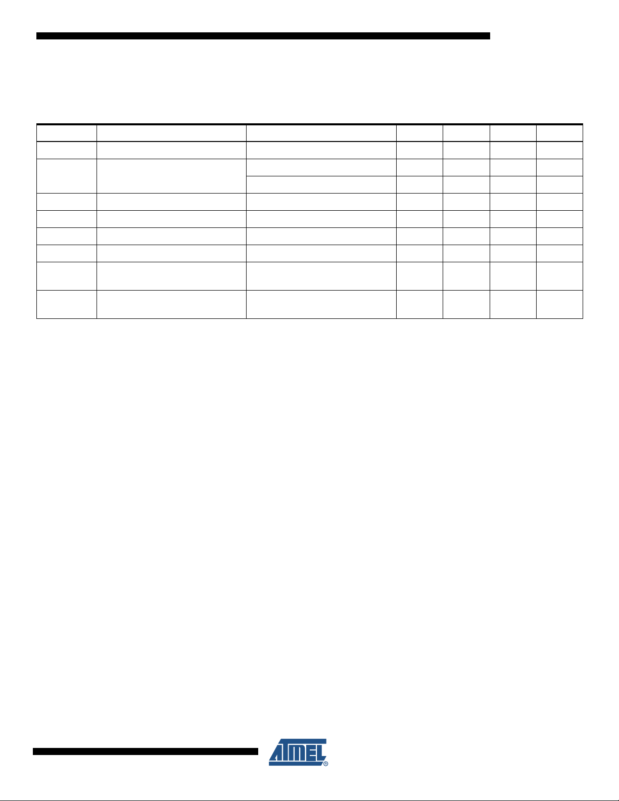
Features
• AUDIO CODEC
– 100dB Dynamic Range Stereo Audio DAC - 8 to 96 kHz sampling frequency
– 96dB Dynamic Range Stereo Audio ADC - 8 to 96 kHz sampling frequency
– 16 / 32 Ohms headset amplifier with capless operation
• SNR: 97 dB A-Weighted
• THD: -60 dB (16Ohms / 20mW / 3.3V supply)
• Maximum output power: 55mW (16Ohms / 3.3V supply)
– Stereo line inputs, stereo auxiliary inputs
– Stereo microphone inputs with bias generator for electret device
– Low power Analog Bypass mode (Line / Aux in to Headset Out)
– Low power Analog sidetone mode (Microphone in to Headset Out)
– Automatic Audio path control with smooth fade in / fade out operation
2
S port
–I
• Master / Slave Operation
2
S / Left / Right justified modes
•I
• 16 / 18 / 20 / 24 bit operation
• 6x SUPPLY CHANNEL VOLTAGE REGULATORS
– DCDC0:
• 1.85V - 600mA. 0.8 to 3.6V / 50mV step.
• 2 MHz switching buck regulator
• Fast load transient response - PWM / PFM modes.
• Efficiency up to 92%
– DCDC1:
• 1.2V - 600mA. 0.8 to 3.6V / 50mV step.
• 2 MHz switching buck regulator
• Fast load transient response - PWM / PFM modes.
• Efficiency up to 90%
– LDO2: 1V - 300mA. 0.8 to 1.35V / 50mV step - Fast transient response
– LDO3: 3.3V - 200mA. 2.7 to 3.6V / 50mV step - Fast transient response
– LDO4: 3.3V - 200mA. 2.7 to 3.6V / 50mV step - Audio codec supply
– LDO5: 2.5V - 10mA - Backup battery charger and RTC supply
• LOW CONSUMPTION POWER MANAGER
– 2.5V - 5.5V VIN Operation
– 20uA typical consumption OFF mode
– VIN monitor, CPU supplies monitor
– Die temperatue and over-current protections
– Reset and Interrupt generation
– Automatic Voltage Ramping on supply channels for DVS applications
– Standby mode with selectable supplies OFF
• RTC
– Ultra Low power crystal oscillator (<1uA typ.)
– Wake up function with programmable alarm or selectable inputs
• 10-b / 300kS/s ADC with 4 external / 6 int\ernal selectable inputs
• Two-Wire Interface for PMU and Audio controls
• Available in 7.5 x 7.5 x 0.9 mm 64-pin QFN Package
• Applications: Multimedia, Audio + Supply solution for MPU+DDR2 designs.
Power
Management
and Analog
Companions
(PMAAC)
AT73C246
6 Supply
Channel PMU
With Audio
Codec
11050A–PMAAC–07-Apr-10
Page 2

1. Description
The AT73C246 is an integrated high performance Power Management and Audio IC. It is specifically designed for advanced technology application processors with complex and low voltage
supplies targeting audio applications from low to high end. This System-on-Chip allows significant savings in both cost and board area over previous discrete solutions.
Directly operated from a 2.9V to 5.5V input voltage, the PMU generates a set of 4 regulated
power supplies and an associated delayed reset signal. These 4 voltages are built up with 2 high
efficiency DCDC buck converters and 2 low noise LDOs. Featuring ultra fast transient responses
and integrating automatic voltage scaling function, these supplies perfectly fit with modern low
voltage MCU cores and memory supplies (DDR, Flash, ...). An additional 200mA LDO under
software control is provided for auxiliary application functions. The high performances of this
LDO (high PSRR, low noise, fast transient response) makes it ideal for analog front-ends (Audio,
RF...) as well digital peripherals.
Aside from the PMU, the AT73C246 integrates a complete state-of-the art low power audio
codec with headphone amplifier. On the input side, a stereo microphone preamplifier with differential or single ended connection (MICDIFF / MIC) and 2 selectable stereo inputs (LINE / AUX)
are directed to a 96dB Dynamic Range stereo audio ADC through an input mixer. On the output
side a 100dB dynamic range stereo audio DAC drives, through an output mixer, a 60 mW stereo
headphone amplifier which comes along with a VCM buffer. This VCM buffer allows to save two
large on-board coupling capacitors for area constrained applications. Additionally two fully analog paths called bypass and sidetone from line / aux and microphone inputs to headphone
outputs allow to reduce the audio power consumption to minimum when needed.
The PMU is complemented with a low power RTC system including a recharging LDO, a crystal
oscillator and a programmable alarm that is fully integrated in the PMU digital core. Thus, the
RTC function is able to wake up the PMU, i.e the regulated power supplies, at a programmed
instant.
Also, a 10-bit ADC equipped with a 10:1 analog multiplexer is provided to the application to perform voltage measurements.
Finally, to reduce power consumption to minimum, the PMU features a flexible STANDBY mode
where the MCU is placed in reset state with selectable supplies ON, OFF or in low-power mode.
Power consumption in OFF mode is typically 20uA.
2
AT73C246
11050A–PMAAC–07-Apr-10
Page 3
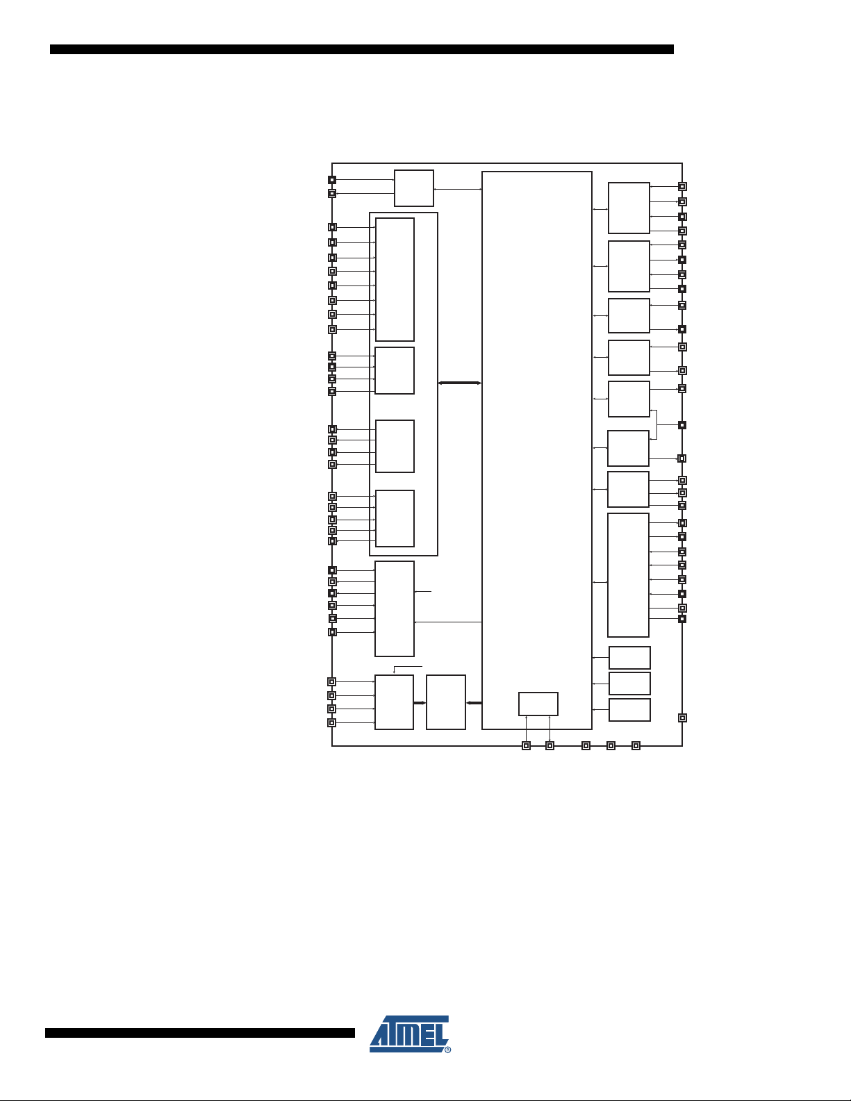
2. Block Diagram
LDO4
3.3V
(CODEC)
AUDIO
CODEC
DIGITAL
CORE
VIN4
VIN0
SW0
VFB0
GND0
BUCK0
1.8V
Max: 600mA
(CORE + MEM)
TWDTWCK
Max: 200mA
VDD4
AVDD
VIN1
SW1
VFB1
GND1
BUCK1
1.2V
Max: 600mA
(CORE)
VIN2
LDO2
1V
Max: 300mA
(CORE)
VDD2
VIN3
LDO3
3.3V
Max: 200mA
(I/O)
VDD3
VINSYS
LDO5
2.5V
Max: 10mA
(BACKUP)
VBACKUP
LDO6
1.8V / 10mA
VDDC
VMID
MICBIAS
AGND
AUDIO
BIAS
LINR
LINL
MICL
AUDIO IN
+ ADC
AUXR
AUXL
HPDET
HPL
HPR
HPVCM
AUDIO OUT
+ DAC
MCLK
LRFS
BCLK
DAI
AUDIO
PORT
DAO
XIN
CLK32K
XOUT
WAKEUP0
RTC +
OSC
PMU
BIAS
REXT
VBG
GNDSYS
ANA0
ANALOG
MUX
ANA1
ANA2
ANA3
10b SAR
ADC
PMU STATE
MACHINES
RSTB
ITB
VPAD
DGND
TWI
DCDC
4MHz RC
OSCILLATOR
WAKEUP1
WAKEUP2
WAKEUP3
HRST
PWREN
VBACKUP
DIE TEMP
SENSOR
SYSTEM
32KHz RC
OSCILLATOR
MICLN
MICR
MICRN
LED
Internal voltages
37
36
28
27
30
29
34
31
33
32
18
35
12
17
13
14
16
15
44
43
42
41
40
63
64
49
62
60
61
3
4
5
6
22 21
26NC47NC48
NC
2
65
45
25
24
23
19
20
11
9
10
8
7
1
39
38
50
51
55
52
54
53
59
56
58
57
NC
46
(Internal
functions)
AT73C246
Figure 2-1. AT73C246 functional block diagram
11050A–PMAAC–07-Apr-10
3
Page 4
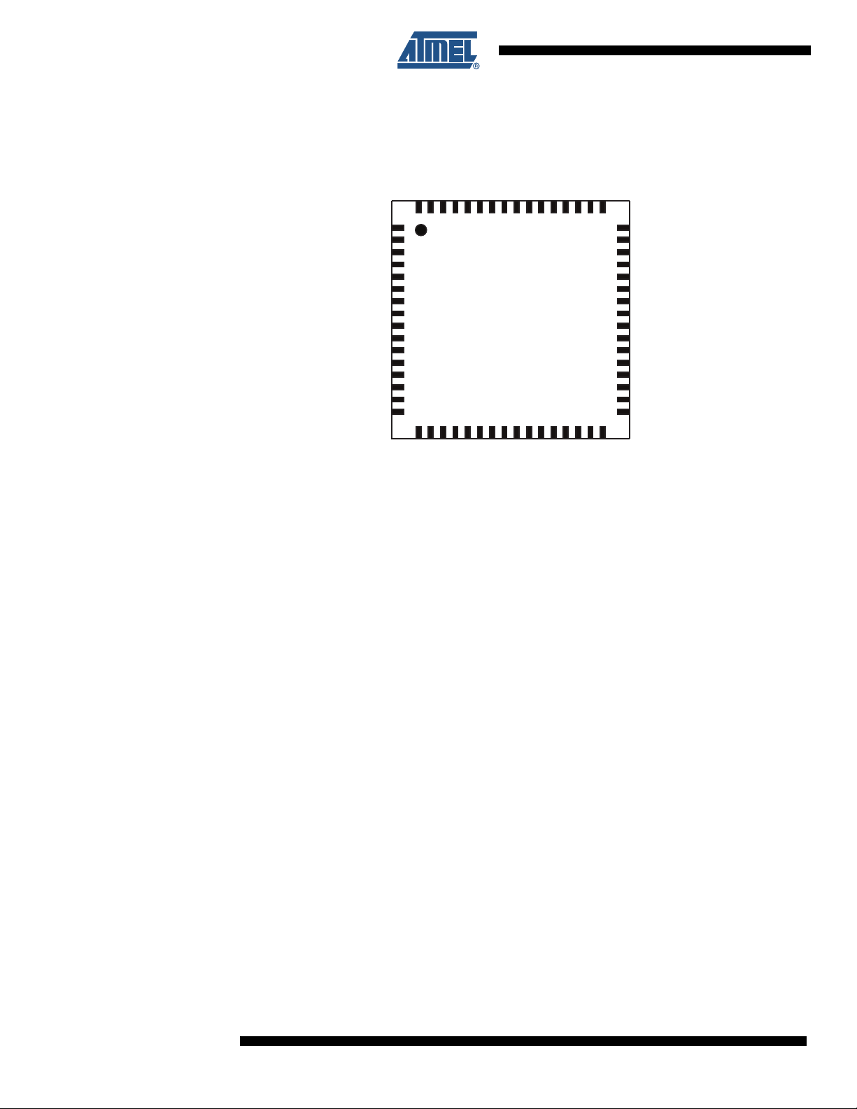
3. Package and Pinout
1
16
17 32
33
48
4964
VBACKUP
LED
ANA0
ANA1
ANA2
ANA3
VINSYS
VDDC
VBG
REXT
GNDSYS
VMID
HPDET
HPR
HPVCM
HPL
AGND
AVDD
ITB
RSTB
TWD
TWCK
WAKEUP1
WAKEUP2
WAKEUP3NCLINR
LINL
AUXR
AUXL
MICLN
MICRN
NC
NC
NC
VPAD
MCLK
LRFS
BCLK
DAI
DAO
VDD3
VIN3
VIN4
VDD4
MICBIAS
MICL
MICR
XOUT
XIN
WAKEUP0
PWREN
HRST
GND0
SW0
VIN0
VFB0
GND1
SW1
VIN1
VFB1
VIN2
VDD2
MCLK32
Figure 3-1. AT73C246 QFN64 package pinout - Top view
4
AT73C246
11050A–PMAAC–07-Apr-10
Page 5

4. Pin Description
Table 4-1. Pin Description
Pin Name I/O Pin Number Type Function
VBACKUP Output 1 Analog RTC supply
AT73C246
LED Output 2 Digital
ANA0 Input 3 Analog Measurement input 0
ANA1 Input 4 Analog Measurement Input 1
ANA2 Input 5 Analog Measurement Input 2
ANA3 Input 6 Analog Measurement Input 3
VINSYS Input 7 Power PMU core supply
VDDC Output 8 Analog
VBG Output 9 Analog PMU Voltage reference
REXT Output 10 Analog
GNDSYS GND 11 Analog PMU ground
VMID Output 12 Analog Audio Codec Mid-Supply reference
HPDET Input 13 Analog Headset detector
HPR Output 14 Analog Headset output right
HPVCM Output 15 Analog Headset virtual ground output
HPL Output 16 Analog Headset output left
AGND GND 17 Analog Audio Codec ground
AVDD Input 18 Power Audio Codec supply input
Output for blinking led. Leave not
connected if a LED is not wired.
PMU / Audio digital supply. Internal use
only. No resistive load.
Resistor connection for PMU bias
current
ITB Output 19 Digital
RSTB Output 20 Digital CPU reset - Active low - Open drain
TWD Input/Output 21 Digital Two Wire Interface - Data
TWCK Input 22 Digital Two Wire Interface - Clock
WAKEUP1 Input 23 Digital
WAKEUP2 Input 24 Digital
WAKEUP3 Input 25 Digital
NC - 26 - Connect to DGND
LINR Input 27 Analog Audio Line input right
LINL Input 28 Analog Audio Line input left
AUXR Input 29 Analog Audio auxiliary input right
AUXL Input 30 Analog Audio auxiliary input left
11050A–PMAAC–07-Apr-10
Interrupt request - Active low - Opendrain
Wake up 1 Input - VPAD level - 100k
Pull down
Wake up 2 Input - VPAD level - 100k
Pull down
Wake up 3 input - VPAD level - 100k
Pull down
5
Page 6
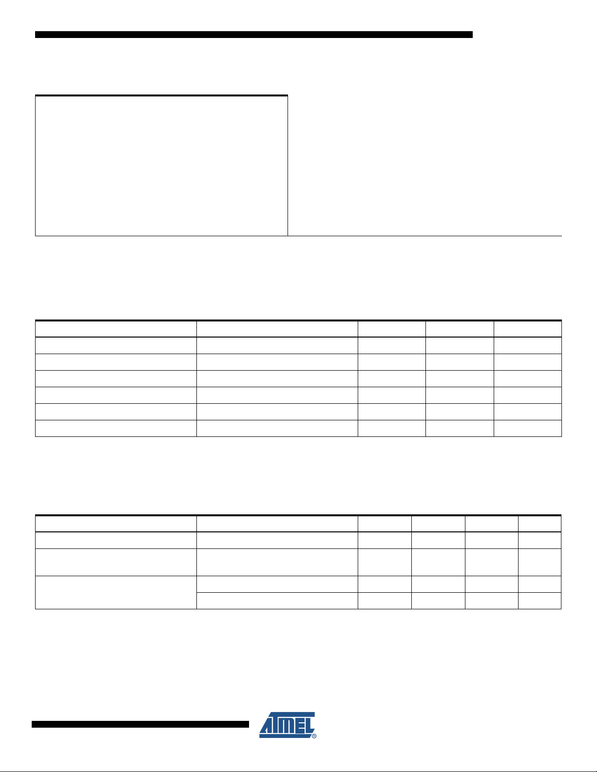
Table 4-1. Pin Description
Pin Name I/O Pin Number Type Function
MICLN Input 31 Analog Audio negative microphone input left
MICRN Input 32 Analog Audio negative microphone input right
MICR Input 33 Analog Audio positive microphone input right
MICL Input 34 Analog Audio positive microphone input left
MICBIAS Output 35 Analog Voltage bias for electret microphone
VDD4 Output 36 Power LDO4 output - 3.3V typ
VIN4 Input 37 Analog LDO4 input
VIN3 Input 38 Power LDO3 input
VDD3 Output 39 Analog LDO3 output - 3.3V typ
DAO Output 40 Digital Digital audio port data output
DAI Input 41 Digital Digital audio port data input
BCLK Input/Output 42 Digital Digital audio port bit clock
LRFS Input/Output 43 Digital Digital audio port left/right clock
MCLK Input 44 Digital Audio codec master clock input
VPAD Input 45 Power PMU I/O ring supply
NC - 46 - Leave open
NC - 47 - Connect to DGND
NC - 48 - Connect to DGND
MCLK32 Output 49 Digital RTC clock output - VPAD level
VDD2 Output 50 Analog LDO2 output
VIN2 Input 51 Power LDO2 input
VFB1 Input 52 Analog DCDC1 Voltage feedback input
VIN1 Input 53 Power DCDC1 power stage supply
SW1 Output 54 Analog DCDC1 power stage output
GND1 Ground 55 Analog DCDC1 power stage ground
VFB0 Input 56 Analog DCDC0 Voltage feedback input
VIN0 Input 57 Analog DCDC0 power stage supply
SW0 Output 58 Analog DCDC0 power stage output
GND0 Ground 59 Analog DCDC0 power stage ground
HRST Input 60 Digital
PWREN Input 61 Digital
WAKEUP0 Input 62 Digital
Hard reset - VBACKUP level - 100k Pull
down
Power on/off - VBACKUP level - 100k
Pull down
Wake up 0 input - VBACKUP level 100k Pull down
6
AT73C246
11050A–PMAAC–07-Apr-10
Page 7

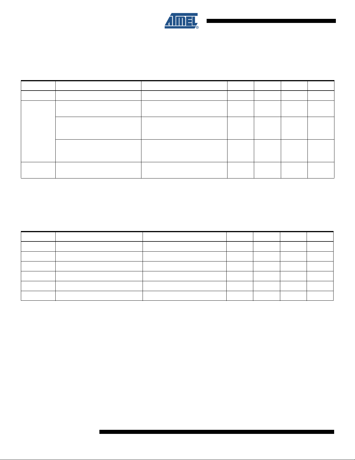
Table 4-1. Pin Description
Pin Name I/O Pin Number Type Function
XIN Input 63 Analog RTC crystal oscillator input
XOUT Output 64 Analog RTC crystal oscillator output
DGND Ground 65 Analog PMU digital ground + Thermal pad.
AT73C246
11050A–PMAAC–07-Apr-10
7
Page 8
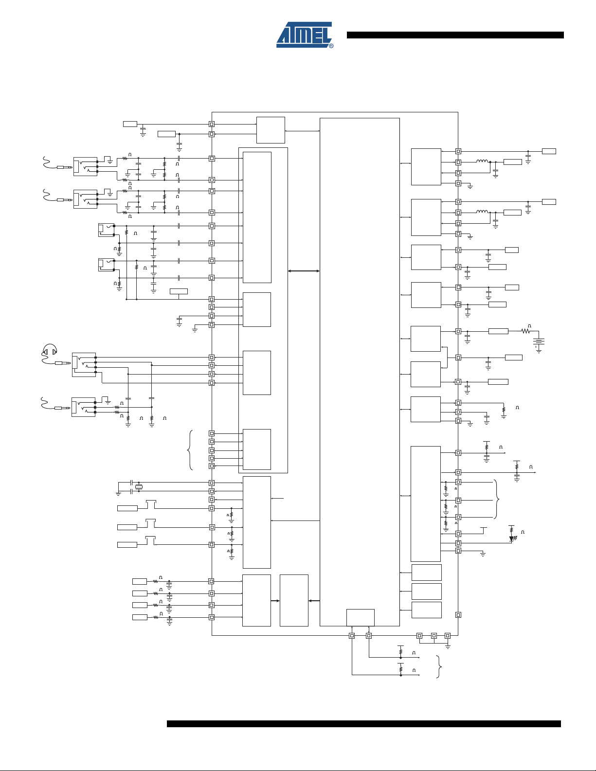
5. Application Block Diagram
1
Figure 5-1. AT73C246 Application Block Diagram
37
1µF
1µF
1µF
1µF
VDD4
I²S
to MCU
3.3µF
C39
3.3µF
C37
3.3µF
C35
3.3µF
C33
C31
C29
C27
C25
AUXL
AUXR
MICL
MICLN
MICR
MICRN
AVDD
MICBIAS
VMID
AGND
HPDET
HPVCM
MCLK
LRFS
BCLK
DAO
XOUT
CLK32K
WAKEUP0
HRST
PWREN
VIN4
LINL
LINR
HPR
36
28
27
30
29
AUDIO IN
34
31
33
32
18
35
12
AUDIO
17
CODEC
13
14
HPL
DAI
XIN
AUDIO OUT
16
15
+DAC
44
43
42
41
40
AUDIO
PORT
63
64
49
62
100K
60
100K
RTC +
61
100K
LINEJACK
J1
AUXJACK
J2
HEADSET 32ohms
J5
LINEOUT
J6
VIN
C42
10µF
VDD4
C41
C40
1nF
C38
1nF
C36
1nF
C34
1nF
R18
2K
PUSHBUTTON
PUSHBUTTON
PUSHBUTTON
10µF
R29
100K
R28
100K
R25
100K
R24
100K
C32
1nF
C30
1nF
C28
1nF
C26
1nF
C23
1µF
C21
3.3µF
R12
100K
X1
S3
S2
S1
100
R30
R31
100
100
R26
R27
100
MIC_L
J3
J4
MIC_R
R22
2K
R23
2K
R19
2K
C22
R14
3.3µF
100
R13
100
100K
R15
C1
9
12
p
C2
0
12p
VBACKUP
VBACKUP
VBACKUP
LDO4
3.3V
Max: 200mA
(CODEC)
+ ADC
BIAS
AUDIO
OSC
VBACKUP
DIGITAL
CORE
BUCK0
1.8V
Max: 600mA
(CORE + MEM)
BUCK1
1.2V
Max: 600mA
(CORE)
LDO2
1V
Max: 300mA
(CORE)
LDO3
3.3V
Max: 200mA
(I/O)
LDO5
2.5V
Max: 10mA
(BACKUP)
LDO6
1.8V / 10mA
(Internal
functions)
PMU
BIAS
PMU STATE
MACHINES
57
VIN0
SW0
VFB0
GND0
VIN1
SW1
VFB1
GND1
VIN2
C6
10µF
VIN3
C8
10µF
C9
2.2µF
VINSYS
C11
2.2µF
REXT
VBG
GNDSYS
RSTB
ITB
WAKEUP1
WAKEUP2
WAKEUP3
VPAD
LED
DGND
L1
2.2µH
L2
2.2µH
VDD0/VDD3
VDD0/VDD3
C2
22µF
C4
22µF
C5
2.2µF
VDD2
C7
10µF
VDD3
VBACKUP
C10
2.2µF
VDDC
C12
22nF
R3
4.7K
C13
10nF
VDD0
VDD1
VDD0
VIN
VINSYS
R2
560k
1%
VDD0/VDD3
From MCU
VIN
D1
R5
470
58
56
59
53
54
52
55
51
50
38
39
1
7
8
10
9
11
20
19
23
100K
24
100K
25
100K
45
2
65
2K
Backup
Battery
R4
4.7K
C14
10nF
VIN
C1
10µF
VIN
C3
10µF
R1
+
BAT
VDD0/VDD3
VDD0/VDD3
DIE TEMP
SENSOR
4MHz RC
OSCILLATOR
SYSTEM
32KHz RC
OSCILLATOR
26 47 48
R6
4.7K
R7
4.7K
DCDC
TWD
TWCK
46
To MCU TWI
NC
R8
ANA_0
ANA_1
ANA_2
ANA_3
100
R9
100
R10
100
R11
100
C15
22nF
C17
22nF
C16
22nF
C18
22nF
ANA0
ANA1
ANA2
ANA3
3
4
5
6
ANALOG
INPUTS
10b SAR
ADC
TWI
22 21
TWDTWCK
8
AT73C246
11050A–PMAAC–07-Apr-10
Page 9
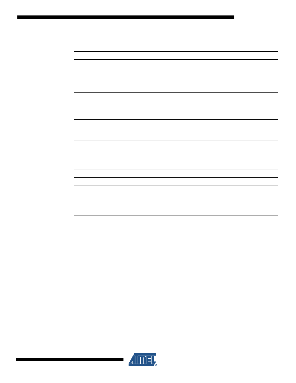
Table 5-1. Typical Application Components Design
Schematic Reference Value Description
R1, R18, R19, R22, R23 2kΩ 5% / 0.063W
R2 560kΩ 1% / 0.063W
R3, R4, R6,R7 4.7kΩ 5% / 0.063W
R5 470Ω 5% / 0.063W
R8, R9, R10, R11, R14, R15,
R26, R27, R30, R31
R12, R13, R24, R25, R28,
R29
100Ω 5% / 0.063W
100kΩ 5% / 0.063W
AT73C246
C1, C3, C6, C7, C8, C10,
C41, C42
C2, C4 22µF
C5, C9, C11 2.2µF X5R / 6.3V
C23, C25, C27, C29, C31 1µF X5R / 6.3V
C13, C14 10nF X5R / 6.3V
C15, C16, C17, C18, C12 22nF X5R / 6.3V
C19, C20 12pF C0G / 25V
C21, C22, C33, C35, C37,
C39
C26, C28, C30, C32, C34,
C36, C38, C40
L1, L2 2.2µH COILCRAFT: LPS3314-222
10µF
3.3µF X5R / 6.3V
1nF X5R
X5R / 6.3V
TDK: C1608X5R0J106MT
MURATA: GRM188R60J106ME47
X5R / 6.3V
TDK: C2012X5R0J226M
MURATA: GRM21BR60J226ME39
11050A–PMAAC–07-Apr-10
9
Page 10

10
AT73C246
11050A–PMAAC–07-Apr-10
Page 11
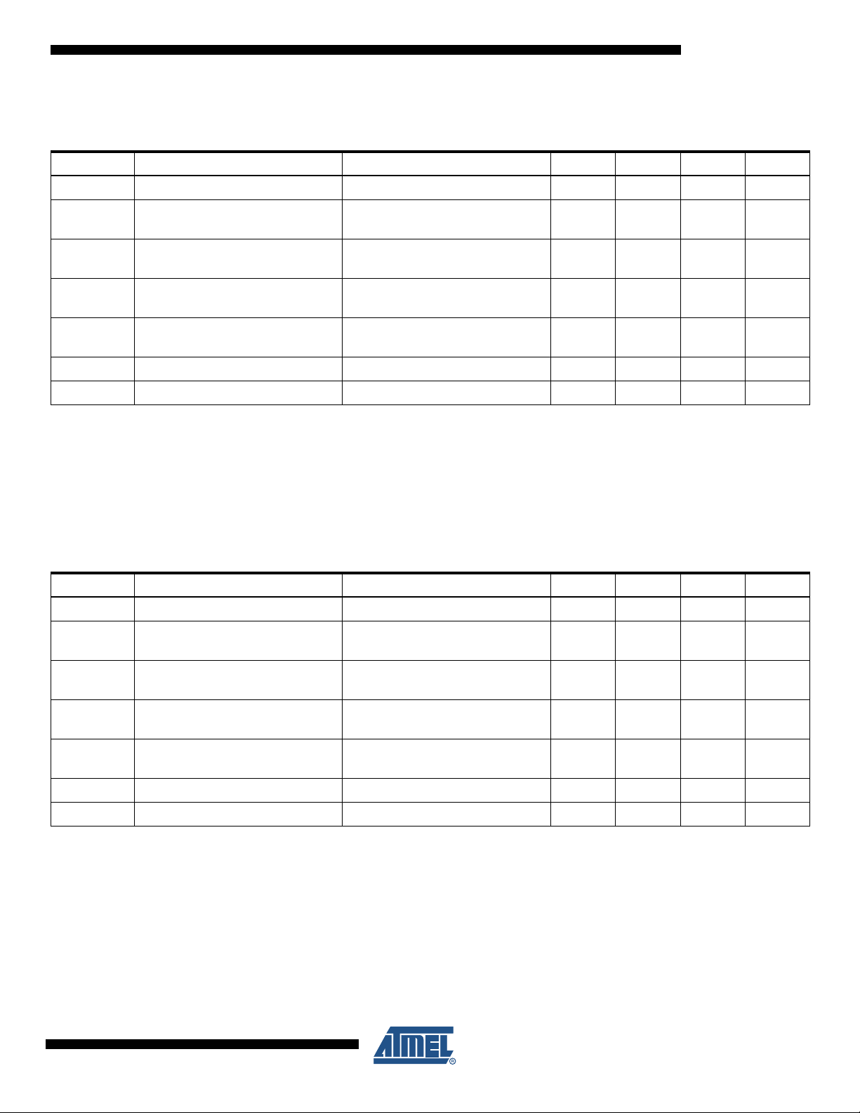
6. Absolute Maximum Ratings
Table 6-1. Absolute Maximum Ratings
Operating Temperature (Industrial).................-40 C to + 85⋅C
Storage Temperature......................................-55°C to + 150°C
Power Supply Input on V
Power Supply Input on V
INSYS
, A
IN2
, V
IN{0,1,3,4}, VPAD
...................... -0.3V to + 3.6V
VDD
Digital I/O Input Voltage...................................... -0.3V to + 5.5V
All Other Pins.......................................................-0.3V to + 5.5V
.. -0.3V to + 5.5V
AT73C246
(1)
*NOTICE: Stresses beyond those listed under “Absolute Maximum
Ratings” may cause permanent damage to the device.
This is a stress rating only and functional operation of
the device at these or other conditions beyond those
indicated in the operational sections of this specification
is not implied. Exposure to absolute maximum rating
conditions for extended periods may affect device reliability.
ESD (all pins).........................................2 KV HBM / 100V MM
(2)
Notes: 1. Refer to Power Dissipation Rating section
2. According to specifications MIL-883-Method 3015.7 (HBM - Human Body Model) / JESD22 A115 (MM - Machine Model)
7. Recommended Operating Conditions
Table 7-1. Recommended Operating Conditions
Parameter Condition Min Max Units
Operating Ambiant Temperature
Power Supply Input V
Power Supply Input V
Power Supply Input V
Power Supply Input A
Power Supply Input V
Note: 1. Refer to Power Dissipation Rating section
(1)
INSYS
IN{0,1,3,4}
IN2
VDD
PAD
-40 85 °C
2.5 5.5 V
2.9 5.5 V
1.65 3.6 V
2.7 3.6 V
1.75 5.5 V
8. Power Dissipation Ratings
Table 8-1. Recommended Operating Conditions
Parameter Condition Min Typ Max Units
Junction Temperature (Tj) -40 125 °C
(1)
R
THjA
Maximum On-chip Power Dissipation
Note: 1. According to specification JESD51-5
11050A–PMAAC–07-Apr-10
Package thermal junction to ambient
resistance
30 35 °C / W
Ambient temperature = 70°C 1.8 1.6 W
Ambient temperature = 85°C 1.3 1.1 W
11
Page 12
9. PMU Electrical Characteristics
9.1 Current Consumption Versus Modes
Table 9-1. Current Consumption Versus Modes
Symbol Parameter Comments Min Typ Max Units
V
IN
Operating Supply Voltage V
POWERDOWN Mode.
INSYS, VIN{0,1,3,4}
present. 2.9 3.6 5.5 V
All LDOs and DCDC converters
OFF. Audio OFF. RTC running.
-2040µA
All LDOs and DCDC converters
I
DD_VIN
RUN Mode.
running in PWM. Audio OFF. RTC
running.
-715mA
Default setup: DCDC0 ON in low-
STANDBY Mode.
power mode. LDO3 ON. All other
-310500µA
functions OFF.
I
DD_RTC
All Modes.
RTC running. Total current
entering pin V
BACKUP
15µA
9.2 Supply Monitor Thresholds
The following table applies to functional state diagrams of Figure 11-1 “AT73C246 Power Man-
ager Functional State Diagram” on page 25 and Figure 11-2 “AT73C246 Start-up and Shutdown
State Diagram” on page 26.
Table 9-2. Supply Monitor Thresholds
Symbol Parameter Comments Min Typ Max Units
> 3.1V PMU Input 3.1V Rising Threshold 3.070 3.1 3.130 V
V
IN
V
< 2.9V PMU Input 2.9V Falling Threshold 2.870 2.9 2.930 V
IN
> 2.7V PMU Input 2.7V Rising Threshold 2.70 2.75 2.85 V
V
IN
< 2.7V PMU Input 2.7V Falling Threshold 2.60 2.65 2.70 V
V
IN
V
> 1.8V V
BKP
< 1.8V V
V
BKP
Input Rising Threshold 1.80 1.85 1.90 V
BACKUP
Input Falling Threshold 1.70 1.75 1.80 V
BACKUP
12
AT73C246
11050A–PMAAC–07-Apr-10
Page 13
9.3 Digital I/Os DC Characteristics
AT73C246
Table 9-3. V
Referred Digital I/Os
PAD
Symbol Parameter Comments Min Typ Max Units
V
PAD
V
IL
V
IH
V
OH
V
OL
I
O
R
P
Notes: 1. V
Operating Supply Voltage 1.75 3.6 5.5 V
Input Low-Level Voltage -0.3 -
Input High-Level Voltage
Output High-Level Voltage IO max.
0.7 x
V
PAD
0.75 x
V
PAD
-
--V
Output Low-Level Voltage IO max - -
Output Current - - 8 mA
Pull-Up or Pull-Down Resistance When applicable. 70 100 145 kΩ
referred pins ITB, RSTB: open drain outputs. Only VOL and IO parameters are applicable.
PAD
2. V
referred pins WAKEUP1, WAKEUP2, WAKEUP3, MCLK, DAI, TWCK: CMOS inputs. Only VIH and VIL parameters are
PAD
0.3 x
V
PAD
V
PAD
0.3
0.25 x
V
PAD
+
applicable.
3. V
4. V
5. V
referred pins MCLK32K, DAO: CMOS outputs. Only VOL, VOH and IO parameters are applicable.
PAD
referred pin TWD: CMOS input and open drain output. Only VIL, VIH, VOL, IO parameters are applicable.
PAD
referred pins LRFS, BCLK: CMOS BiDir. All parameters applicable
PAD
V
V
V
Table 9-4. V
Referred Digital I/Os
BACKUP
Symbol Parameter Comments Min Typ Max Units
V
BACKUP
V
IL
V
IH
V
OH
V
OL
I
O
R
P
Note: V
Operating Supply Voltage 1.75 2.5 2.65 V
Input Low-Level Voltage -0.3 -
Input High-Level Voltage
Output High-Level Voltage IO max.
0.7 x
V
BACKUP
0.75 x
V
BACKUP
Output Low-Level Voltage IO max - -
-
--V
0.3 x
V
BACKUP
V
BACKUP
+ 0.3
0.25 x
V
BACKUP
Output Current - - 8 mA
Pull-Up or Pull-Down resistance When applicable. 70 100 145 kΩ
referred pins PWREN, HRST, WAKEUP0: CMOS inputs. Only VIL and VIH parameters are applicable.
BACKUP
V
V
V
11050A–PMAAC–07-Apr-10
13
Page 14
9.4 DCDC0 and DCDC1
Unless otherwise specified: External components L=2.2μH, C
T
= [-40°C ; +125°C].
J
Table 9-5. DCDC0 and DCDC1 Electrical Characteristics
Symbol Parameter Comments Min Typ Max Units
V
IN
I
DD
I
O
Operating Supply Voltage V
Supply Current
(1)
Output Current
, V
IN1
and V
IN0
OFF - - 1 µA
PFM operation.
= 1.85V, V
V
DD0
PWM operation.
V
= 1.85V, V
DD0
PFM operation. - - 50 mA
PWM operation. - - 600 mA
=22μF and CIN=10μF. V
OUT
2.9 3.6 5.5 V
INSYS
DD1
DD1
= 1.2V
= 1.2V
-
-
IN{0,1}
> V
DD{0,1}
+ 500mV.
40 80 µA
36.5mA
f
SW
V
DD0
V
DD1
V
DD_RANGE
V
DD_STEP
N
STEP
T
STEP
V
DD_ACC
V
DD_RIPPLE
Switching Frequency PWM operation. 1.8 2 2.2 MHz
Default Output Voltage
Programmable Output Voltage
Range
Output Voltage Steps PFM or PWM operation. 50 mV
Number of Output Steps
Step time With automatic ramping. 260 280 300 µs
DC Output Voltage Accuracy
Ripple Voltage PWM operation. 2 mV
Static Load Regulation
Δ
VDD_IL
Dynamic Load Regulation
Δ
VDD_VIN
Static Line Regulation
Eff Efficiency
I
INRUSH
Inrush Current
V
(2)
DD0
V
DD1
-1.85- V
-1.2- V
PFM or PWM operation. 0.8 3.6 V
In case of direct output voltage
programming. Automatic ramping
4
not active.
PFM; T
PFM; T
PWM; T
PWM; T
PWM operation. I
to I
PWM. IO: 0 to I
PWM. I
V
V
PWM. I
Relative to V
PWM. I
Relative to V
Current from V
(1)
from 0 to 100% V
V
= 25°C ; IO = 0 mA -1.5 2.5
J
= [-40;125°C] ; IO = 0 mA -2 3
J
= 25°C ; IO = 0 mA -1.5 1.5
J
= [-40;125°C] ; IO = 0 mA -2 2
J
ranging from 0
O
OMAX
; 1μs rise time -40
OMAX
: I
O
and V
IN0
= 1.85V, V
DD0
OMAX
OMAX
= 1.85V, V
DD0
to 0 ; 1μs fall time 40
OMAX
from 2.9 to 5.5V
INSYS
= 1.2V
DD1
load. V
input supply.
IN0
load. V
input supply.
IN1
IN(0,1)
DD{0,1}
DD1
= 1.85V.
DD0
= 1.2V.
DD1
and V
= 1.2V
INSYS
25mV
5mV
85 %
78 %
30 200 mA
step /
100µs
%
mV
14
AT73C246
11050A–PMAAC–07-Apr-10
Page 15
AT73C246
Table 9-5. DCDC0 and DCDC1 Electrical Characteristics
Symbol Parameter Comments Min Typ Max Units
OCP Over-Current Protection Output current. 1 1.4 1.8 A
T
START
T
PWM
PWRF
C
OUT
DET
Start-up Time
PFM to PWM Settling Time No output load. 10 µs
Power Fail Detector Threshold
Accuracy
Total Capacitive Load At V
Notes: 1. Current consumption without load. One DCDC converter ON, the other one OFF.
2. Default output voltage are set during manufacturing. Please contact Atmel for other default settings.
3. Threshold levels are programmed in register PMU_RST_LVL (0x04)
From OFF to PWM operation.
rising to 95% of final value.
V
DD(0,1)
Overload of the programmed
threshold by 10mV / 5us min
pins. 8 36 µF
FB{0,1}
5ms
(3)
.
-1 - +1 %.V
DD
11050A–PMAAC–07-Apr-10
15
Page 16

9.5 LDO2
Unless otherwise specified: External components C
Table 9-6. LDO2 Electrical Characteristics
Symbol Parameter Comments Min Typ Max Units
V
IN
I
DD
I
O
V
DD2
V
DD_RANGE
Operating Supply Voltage V
Supply Current
(1)
Output Current V
Default Output Voltage
(2)
Programmable Output Voltage
Range
OFF - - 1 µA
ON - - 250 µA
=10µF, CIN=10μF, TJ = [-40°C ; +125°C].
OUT
IN2
> V
IN2
+ 500mV. - - 300 mA
DD2
1.65 1.8 3.6 V
-1-V
0.8 1.35 V
V
DD_STEP
T
STEP
V
DD_ACC
Output Voltage Steps 50 mV
Step time With automatic ramping. 570 600 630 µs
DC Output Voltage Accuracy
Static Load Regulation
Δ
VDD_IL
Dynamic Load Regulation
Δ
VDD_VIN
V
DROPOUT
I
INRUSH
T
START
PWRF
DET
Static Line Regulation
Drop Out Voltage
(4)
Inrush Current
Start-up Time
Power Fail Detector Threshold
Accuracy
Notes: 1. Current consumption in V
2. Default output voltage are set during manufacturing. Please contact Atmel for other default settings.
3. Threshold level is programmed in register PMU_RST_LVL (0x04)
4. V
DROPOUT
= V
IN2
- V
when V
DD2
without load.
IN2
= 98% of V
DD2
> V
V
IN2
= 25°C ; IO = 0 mA
T
J
V
IN2
= [-40°C ; 125°C] ; IO = 0 mA
T
J
V
IN2
ranging from 0 to I
I
O
V
IN2
0 to I
I
O:
V
IN2
I
O: IOMAX
I
= 0 mA
O
V
IN2
+ 500mV
DD2
> V
+ 500mV
DD2
> V
+ 500mV
DD2
> V
+ 500mV
DD2
; 1μs rise time
OMAX
> V
+ 500mV
DD2
to 0 ; 1μs fall time
from 1.65 to 3.6V
-1 1
%
-1.5 1.5
0.05 1 %.V
OMAX
-50
mV
50
5mV
IO = 200mA 300 mV
I
= 300mA 450 mV
O
Current from V
final value.
V
OFF and rising to 95% of
DD2
final value. I
Overload of the programmed
threshold by 10mV / 5us min
obtained with V
DD2
from 0 to 95% of
IN2
= 0 mA
O
IN2
> V
(3)
.
DD2
200 500 mA
1ms
-1 - +1 %.V
+ 500mV
DD2
DD2
16
AT73C246
11050A–PMAAC–07-Apr-10
Page 17
AT73C246
9.6 LDO3
Unless otherwise specified: External components C
Table 9-7. LDO3 Electrical Characteristics
Symbol Parameter Comments Min Typ Max Units
V
IN
I
DD
I
O
V
DD3
V
DD_RANGE
Operating Supply Voltage V
Supply Current
(1)
Output Current V
Default Output Voltage
(2)
Programmable Output Voltage
Range
=10µF, CIN=10μF, TJ = [-40°C ; +125°C].
OUT
IN3
2.9 3.6 5.5 V
OFF - - 1 µA
ON - - 350 µA
> V
IN3
+ 300mV. - - 200 mA
DD3
-3.3- V
2.7 3.6 V
V
DD_STEP
T
STEP
V
DD_ACC
Output Voltage Steps 50 mV
Step time With automatic ramping. 570 600 630 µs
DC Output Voltage Accuracy
Static Load Regulation
Δ
VDD_IL
Dynamic Load Regulation
Δ
VDD_VIN
V
DROPOUT
Static Line Regulation
Drop Out Voltage
(4)
PSRR Power Supply Rejection Ratio
I
INRUSH
Inrush Current
> V
V
IN3
= 25°C ; IO = 0 mA
T
J
V
IN3
= [-40°C ; 125°C] ; IO = 0 mA
T
J
V
IN3
ranging from 0 to I
I
O
V
IN3
0 to I
I
O:
V
IN3
I
O: IOMAX
V
IN3
V
IN3
+ 300mV
DD3
> V
+ 300mV
DD3
> V
+ 300mV
DD3
> V
+ 300mV
DD3
; 1μs rise time
OMAX
> V
DD3
+ 300mV
to 0 ; 1μs fall time
> V
+ 300mV. IO = 0 mA
DD3
from 2.9 to 5.5V
-1 1
%
-1.5 1.5
0.05 0.5 %.V
OMAX
-40
mV
40
5mV
IO = 10mA 50 mV
I
= 200mA 250 mV
O
V
> V
> V
+ 300mV
DD3
+ 300mV
DD3
from 0 to 95%
IN3
60
dB
50
200 500 mA
IN3
= 1mA. DC to 3kHz.
I
O
V
IN3
= 10mA. DC to 3kHz.
I
O
Current from V
of final value.
DD3
T
START
PWRF
DET
Start-up Time
Power Fail Detector Threshold
Accuracy
Notes: 1. Current consumption in V
2. Default output voltage are set during manufacturing. Please contact Atmel for other default settings.
3. Threshold level is programmed in register PMU_RST_LVL (0x04)
4. V
DROPOUT
11050A–PMAAC–07-Apr-10
= V
IN3
- V
when V
DD3
without load.
IN3
= 98% of V
DD3
V
OFF and rising to 95% of
DD3
final value. I
= 0 mA
O
Overload of the programmed
threshold by 10mV / 5us min
obtained with V
DD3
IN3
> V
(3)
.
DD3
-1 - +1 %.V
+ 300mV
1ms
DD3
17
Page 18
9.7 LDO4
Unless otherwise specified: External components C
Table 9-8. LDO4 Electrical Characteristics
Symbol Parameter Comments Min Typ Max Units
V
IN
I
DD
I
O
V
DD4
V
DD_RANGE
Operating Supply Voltage V
Supply Current
(1)
Output Current V
Default Output Voltage
(2)
Programmable Output Voltage
Range
=10µF, CIN=10μF, TJ = [-40°C ; +125°C].
OUT
IN4
2.9 3.6 5.5 V
OFF - - 1 µA
ON - - 350 µA
> V
IN4
+ 300mV. - - 200 mA
DD4
-3.3- V
2.7 3.6 V
V
DD_STEP
T
STEP
V
DD_ACC
Output Voltage Steps 50 mV
Step time With automatic ramping. 570 600 630 µs
DC Output Voltage Accuracy
Static Load Regulation
Δ
VDD_IL
Dynamic Load Regulation
Δ
VDD_VIN
V
DROPOUT
Static Line Regulation
Drop Out Voltage
(3)
PSRR Power Supply Rejection Ratio
I
INRUSH
Inrush Current
> V
V
IN4
= 25°C ; IO = 0 mA
T
J
V
IN4
= [-40°C ; 125°C] ; IO = 0 mA
T
J
V
IN4
ranging from 0 to I
I
O
V
IN4
0 to I
I
O:
V
IN4
I
O: IOMAX
V
IN4
V
IN4
+ 300mV
DD4
> V
+ 300mV
DD4
> V
+ 300mV
DD4
> V
+ 300mV
DD4
; 1μs rise time
OMAX
> V
DD4
+ 300mV
to 0 ; 1μs fall time
> V
+ 300mV. IO = 0 mA
DD4
from 2.9 to 5.5V
-1 1
%
-1.5 1.5
0.05 0.5 %.V
OMAX
-40
mV
40
5mV
IO = 10mA 50 mV
I
= 200mA 250 mV
O
V
> V
> V
+ 300mV
DD4
+ 300mV
DD4
from 0 to 95%
IN4
60
dB
50
200 500 mA
IN4
= 1mA. DC to 3kHz.
I
O
V
IN4
= 10mA. DC to 3kHz.
I
O
Current from V
of final value.
DD4
T
START
Start-up Time
Notes: 1. Current consumption in V
2. Default output voltage are set during manufacturing. Please contact Atmel for other default settings.
18
3. V
DROPOUT
AT73C246
= V
IN4
- V
when V
DD4
without load.
IN4
= 98% of V
DD4
V
OFF and rising to 95% of
DD4
final value. I
DD4
= 0 mA
O
obtained with V
IN4
> V
+ 300mV
DD4
1ms
11050A–PMAAC–07-Apr-10
Page 19
AT73C246
9.8 LDO5
Unless otherwise specified: External components C
Table 9-9. LDO5 Electrical Characteristics
Symbol Parameter Comments Min Typ Max Units
V
IN
I
DD
I
O
V
BACKUP
Δ
VDD_VIN
Δ
VDD_VIN
I
INRUSH
T
START
Note: 1. Current consumption in V
Operating Supply Voltage V
Supply Current
(1)
Output Current - - 10 mA
Output Voltage Accuracy 2.42 2.5 2.58 V
Static Line Regulation V
Static Line Regulation V
Inrush Current
Start-up Time
without plugged backup battery
INSYS
=2.2µF, CIN=10μF, TJ = [-40°C ; +125°C].
OUT
INSYS
2.7 3.6 5.5 V
OFF - - 1 µA
ON - - 7 µA
from 2.7 to 5.5V 3 10 mV
INSYS
=3.6V, IO from 0 to I
INSYS
Current from V
T
START(MAX)
V
BACKUP
. V
OFF and rising to 95% of
final value.
INSYS
BACKUP
OMAX
from 0 to
= 2.5V
10 15 mV
180 350 mA
1ms
11050A–PMAAC–07-Apr-10
19
Page 20
9.9 Measurement Bridge and 10-bit ADC
Table 9-10. Measurement Bridge and 10-bit ADC Electrical Characteristics
Symbol Parameter Comments Min Typ Max Units
V
IN
I
DD
V
REF
Operating Supply Voltage
Supply Current
Reference Voltage
INL Integral Non Linearity End Point Method -2 - +2 LSB
DNL Differential Non Linearity End Point Method -1 - +1 LSB
Offset Offset Error -2 +2 LSB
GAIN Gain Error -2 +2 LSB
F
S
T
ACQ
V
MEAS
ATT
R
IN_NOM
R
IN_TEMP
C
IN
MEAS
Sampling Rate 300 kS/s
Track and Hold Acquisition Time 500 ns
Measured Input Voltage Range
Measured Input Scaling Factor
ANA{0,1,2,3} Input resistance Tj = 25C 96 120 144 kΩ
RIN deviation with temperature
ANA{0,1,2,3} Input capacitance 15 pF
Notes: 1. The 10-bit ADC is supplied from the regulated V
2. Please refer to Atmel Data Converter Terminology literature
(1)
V
INSYS
2.9 3.6 5.5 V
OFF - - 1 µA
ON - - 2 mA
Internally connected to
VDDC pin.
External inputs ANA{0,1,2,3} 0.4 V
V
DD{0,1,2,3,4}
V
INSYS
inputs 0.4 4 V
input 0.4 5.5 V
1.75 1.8 1.85 V
INSYS
External inputs ANA{0,1,2,3} -1% 0.25 +1% V/V
V
DD{0,1,2,3,4,5}
V
INSYS
T
[-40 ; +25]. Relative to
J
R
IN_NOM
TJ [25 ; 125]. Relative to
R
IN_NOM
inputs -1% 0.4 +1% V/V
input -1% 0.25 +1% V/V
+ 20
-16
voltage (1.8V) which is generated from V
DDC
INSYS
.
V
%
20
AT73C246
11050A–PMAAC–07-Apr-10
Page 21
AT73C246
9.10 RTC Crystal Oscillator
Table 9-11. RTC Crystal Oscillator Electrical Characteristics
Symbol Parameter Comments Min Typ Max Units
V
IN
Operating Supply Voltage V
BACKUP
Freq Frequency with crystal - 32.768 - kHz
Duty Duty Cycle 40 50 60 %
I
DD
T
V
V
R
ON
XIN
XOUT
F
Supply Current
(1)
Star tup Time CL= 12pF - 1000 1500 ms
Level Sinus Wave on XIN 250 300 mVpp
Vpp On XOUT 300 mVpp
Internal Resistor between xin and xout 10 MΩ
OFF - - 5 nA
ON - - 1.5 µA
Drift Accuracy @25°C, +/- 20ppm 1.5 mn/month
Esr Equivalent Series Resistance Rs Crystal @ 32.768kHz 50 100 kΩ
C
M
C
SHUNT
C
LOAD
Note: 1. Current consumption in V
Motional Capacitance Crystal @ 32.768kHz 0.6 3 fF
Shunt Capacitance Crystal @ 32.768kHz 0.6 2 pF
Load Capacitance Crystal @ 32.768kHz 6 12.5 pF
with crystal. In case of crystal not present on-board, back-up batteries or supercapacitors,
BACKUP
must be avoided.
1.75 2.5 2.65 V
9.11 Die Temperature Sensor
Table 9-12. Die Temperature Sensor Electrical Characteristics
Symbol Parameter Comments Min Typ Max Units
T
SHUTDOWN
T
RESTART
130°C Shutdown Threshold 135 145 155 °C
110°C Restart Threshold 105 115 125 °C
11050A–PMAAC–07-Apr-10
21
Page 22
10. Audio Codec Electrical Characteristics
Unless otherwise specified: AVDD = 3.3V, TA = 25C, MCLK = 12.288MHz, FS = 48kHz. Master mode and 24-bit operation
2
on I
S port. All gains set to 0dB, audio effects are off. Noise measurements are made in the [20Hz-20kHz] band using the
A-Weighting filter. Distortion measurements are made from the 2
Input sources have an internal impedance of 50 Ohms. Audio Path without mixing capability.
Table 10-1. Audio Codec Bias
Symbol Parameter Comments Min Typ Max Units
AVDD Operating Supply Voltage 2.7 3.3 3.6 V
nd
to the 5th harmonic products of a 997Hz input sinewave.
I
DD
V
MID
T
MID_ON
T
MID_OFF
V
MICBIAS
R
MICBIAS
Supply Current
STANDBY 1 mA
Mid-Supply Reference Voltage -1%
Time to charge V
Time to discharge V
Microphone Bias Reference
Voltage
Microphone Bias Reference
Voltage Internal Resistance
capacitor From 0 to 95% of final value 350 ms/μF
MID
capacitor From 0 to 95% of final value 700 ms/μF
MID
No load. AVDD V
1.5 1.9 2.3 kΩ
AVDD /
2
+1% V
Table 10-2. Line Record Path: Line or Auxiliary Input to ADC Output
Symbol Parameter Comments Min Typ Max Units
OFF 20 µA
V
FS
Full Scale Input Voltage
SNR Signal-to-Noise Ratio
(1)
(2)
Corresponds to 0dBFs digital
output signal.
AVDD = 3.3V 85 96 - dB
AVDD = 2.7V 82 93 - dB
DR Dynamic Range
(3)
AVDD = 3.3V 85 96 - dB
AVDD = 2.7V 82 93 - dB
THD Total Harmonic Distortion -1dBFS digital output - -80 -74 dB
XTALK Left / Right Channel separation
(5)
80 90 - dB
Programmable Gain Range -34 0 12 dB
G
LINE
R
IN
C
IN
Gain Step Size - 1 - dB
Mute Attenuation
(6)
80 - - dB
Input Resistance 5.9 7 8.1 kΩ
Input Capacitance - - 10 pF
AVDD /
3.3
V
RMS
Table 10-3. Microphone Record Path: Microphone Input to ADC Output
Symbol Parameter Comments Min Typ Max Units
V
FS
Full Scale Input Voltage
SNR Signal-to-Noise Ratio
22
AT73C246
(1)
Corresponds to 0dBFs digital
output signal.
(2)
AVDD = 3.3V 85 96 - dB
AVDD = 2.7V 82 93 - dB
AVDD /
3.3
V
11050A–PMAAC–07-Apr-10
RMS
Page 23
AT73C246
Table 10-3. Microphone Record Path: Microphone Input to ADC Output
Symbol Parameter Comments Min Typ Max Units
DR Dynamic Range
(3)
THD Total Harmonic Distortion -1dBFS digital output - -84 -74 dB
XTALK Left / Right Channel separation
Programmable Gain Range 0 - 46 dB
G
LINE
Gain Step Size - 1 - dB
Mute Attenuation
(6)
AVDD = 3.3V 85 96 - dB
AVDD = 2.7V 82 93 - dB
(5)
80 90 - dB
80 - - dB
R
IN
C
IN
Input Resistance 0dB gain 8.4 12 15.6 kΩ
Input Capacitance - - 10 pF
Table 10-4. Playback Path: DAC Input to Headphone Output
Symbol Parameter Comments Min Typ Max Units
V
FS
Full Scale Output Voltage
SNR Signal-to-Noise Ratio
DR Dynamic Range
(3)
(1)
(2)
THD Total Harmonic Distortion
P
O
Output Power
XTALK Left / Right Channel Separation
Programmable Gain Range -77 - +6 dB
G
HS
Gain Step Size - 1 - dB
Mute Attenuation
(6)
0dBFs digital input signal.
AVDD = 3.3V 92 97 - dB
AVDD = 2.7V 89 94 - dB
AVDD = 3.3V 92 97 - dB
AVDD = 2.7V 89 94 - dB
0dBFs input - 10kΩ load - -88 -80 dB
20mW output - 32Ω load - -65 -60 dB
20mW output - 16Ω load - -60 -55 dB
32Ω load - THD < -40dB or 1% 30 mW
16Ω load - THD < -40dB or 1% 50 mW
10kΩ AC coupled load 90 dB
(5)
16Ω DC coupled load 60 dB
80 - - dB
AVDD /
3.3
V
RMS
Table 10-5. Analog Bypass Path: Line / Auxiliary Input to Headphone Output
Symbol Parameter Comments Min Typ Max Units
V
FS
Full Scale Output Voltage
SNR Signal-to-Noise Ratio
DR Dynamic Range
11050A–PMAAC–07-Apr-10
(3)
(1)
(2)
AVDD = 3.3V 92 97 - dB
AVDD = 2.7V 89 94 - dB
AVDD = 3.3V 92 97 - dB
AVDD = 2.7V 89 94 - dB
AVDD /
3.3
V
RMS
23
Page 24
Table 10-5. Analog Bypass Path: Line / Auxiliary Input to Headphone Output
Symbol Parameter Comments Min Typ Max Units
0dBFs input - 10kΩ load - -88 -80 dB
THD Total Harmonic Distortion
P
O
Output Power
XTALK Left / Right Channel Separation
20mW output - 32Ω load - -65 -60 dB
20mW output - 16Ω load - -60 -55 dB
32Ω load - THD < -40dB or 1% 30 mW
16Ω load - THD < -40dB or 1% 50 mW
10kΩ AC coupled load 90 dB
(5)
16Ω DC coupled load 60 dB
G
BYP
Mute Attenuation
(6)
80 - - dB
Table 10-6. Analog Sidetone Path: Microphone Input to Headphone Output
Symbol Parameter Comments Min Typ Max Units
Bypass Gain -1 0 +1 dB
V
FS
Full Scale Output Voltage
SNR Signal-to-Noise Ratio
(1)
(2)
AVDD = 3.3V 92 97 - dB
AVDD = 2.7V 89 94 - dB
DR Dynamic Range
(3)
AVDD = 3.3V 92 97 - dB
AVDD = 2.7V 89 94 - dB
0dBFs input - 10kΩ load - -88 -80 dB
THD Total Harmonic Distortion
20mW output - 32Ω load - -65 -60 dB
20mW output - 16Ω load - -60 -55 dB
32Ω load - THD < -40dB or 1% 30 mW
P
O
XTALK Left / Right Channel Separation
Output Power
16Ω load - THD < -40dB or 1% 50 mW
10kΩ AC coupled load 90 dB
(5)
16Ω DC coupled load 60 dB
Programmable Gain Range -30 - 0 dB
G
SIDETONE
Gain Steps 2.5 3 3.5 dB
Mute Attenuation
(6)
Notes: 1. Full Scale: A linear extrapolation to 0dBFS of the measured level at -10dBFS.
2. Signal-to-Noise Ratio: The ratio of the RMS value of a 997Hz full scale sine wave to the RMS value of output noise with no
signal applied. Device is not muted.
3. Dynamic Range: According to AES17-1991 (Audio Engineering Society) and EIAJ CP-307 (Electronic Industries Association of Japan), an extrapolation to 0dBFS input signal of the THD+N ratio measurement at -60dBFS. As an example, if
THD+N @ -60dBFS = -36dB, then DR = 96dB.
4. Total Harmonic Distortion + Noise Ratio: The ratio of the RMS sum of the noise and the distortion components to the RMS
value of the signal.
5. XTALK: Attenuation measurement from one channel to the other one. Measurement is performed by stimulated one channel
with a 997Hz / -10dBFS sinewave and leaving the other channel unstimulated.
6. Mute Attenuation: Attenuation measurement of a -10dBFS / 997Hz input signal when concerned gain is set to mute.
80 - - dB
AVDD /
3.3
V
RMS
24
AT73C246
11050A–PMAAC–07-Apr-10
Page 25
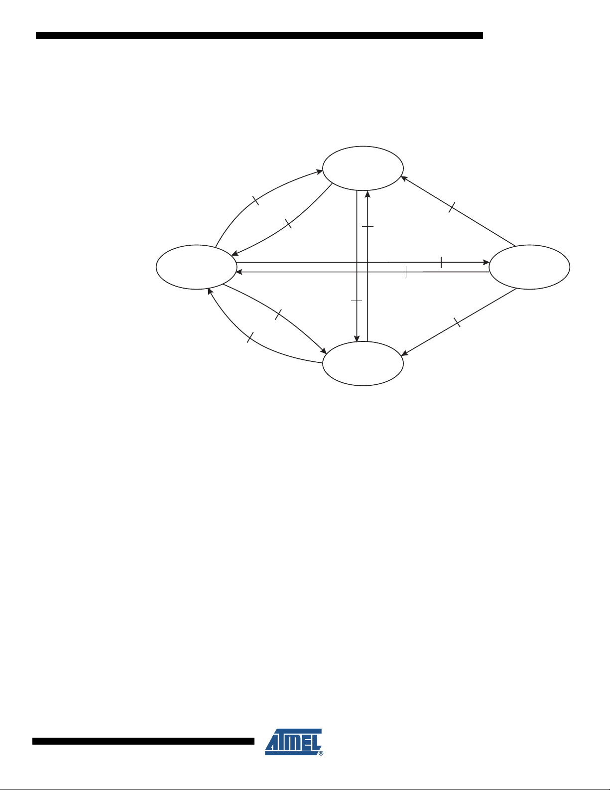
11. PMU Functional Description
POWERDOWN
(all supplies OFF)
RSTB = 0
HRST
(all supplies OFF)
RSTB = 0
TWI Reset
STANDBY
(selected supplies ON)
RSTB = 0
RUN
(all supplies ON)
RSTB = 1
POWER-OFF or POWER-FAIL
EVENT
POWER-ON EVENT &
Vin > 3.1V
HRST_POWERDOWN
EVENT
HRST_RUN
EVENT
HRST
EVENT
WAKEUP
EVENT
STANDBY
EVENT
HRST
EVENT
HRST
EVENT
STANDBY-OUT or POWER-FAIL
EVENT
11.1 Power Manager State Diagram
Figure 11-1. AT73C246 Power Manager Functional State Diagram
AT73C246
AT73C246 is placed in POWERDOWN state at VINSYS rising following the PMU startup state
diagram described in Figure 11-2 on page 26. From this POWERDOWN state, normal CPU supplies startup is achieved through validation of one of the POWER-ON events. From this state,
the PMU may be placed in STANDBY state (e.g.: during CPU sleep periods) upon software
request (STANDBY event). PMU wake-up is achieved if one of the WAKEUP events is detected.
The PMU returns to the POWERDOWN state as soon as a POWER-OFF event is detected. A
special HRST (Hard-Reset) state is provided to ensure complete stop and restart of the CPU
supplies in case of a software crash. Moreover, die temperature and VDD
supervised and may generate a POWER-FAIL event in case of out-of-specification detection.
{0,1,2,3}
supplies are
11050A–PMAAC–07-Apr-10
25
Page 26
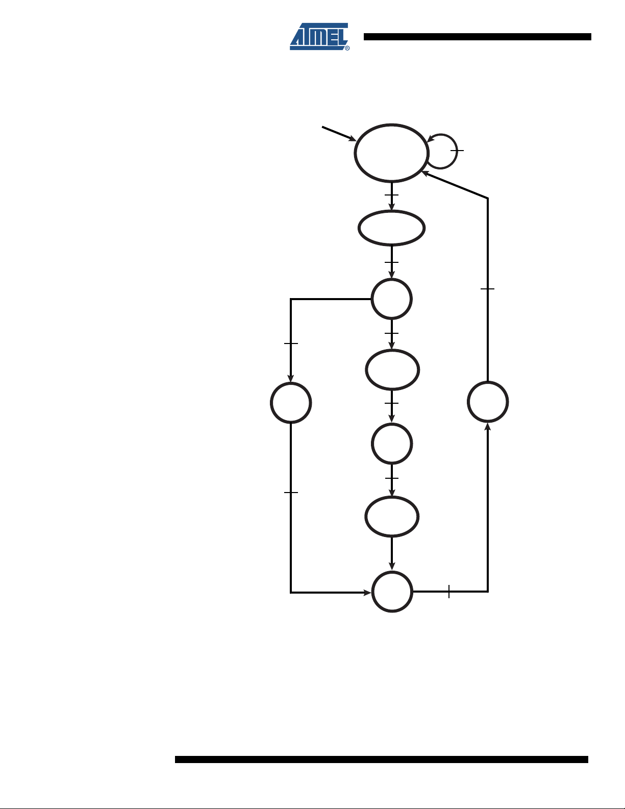
11.2 PMU Startup and Shutdown State Diagram
Start : V
INSYS
Monitor &
V
DDC
= 1.8V.
PMU_RSTN = 0
AUDIO_RSTN = 0
V
INSYS
< 2.7V
or
V
DDC
_KO
Vin > 2V
VINSYS > 2.7V &
V
DDC
_OK
PMU_RSTN = 1
AUDIO_RSTN = 1
1
READ
CONFIG
V
BACKUP
< 1.8V
RTC_RSTN = 0
1
START
LDO5
(BACKUP)
V
BACKUP
> 1.8V
RTC_RSTN = 1
POWER
DOWN
V
BACKUP
> 1.8V
START
LDO5
(BACKUP)
V
BACKUP
> 1.8V
V
INSYS
< 2.7V
OFF
LDO5
(BACKUP)
1
Figure 11-2. AT73C246 Start-up and Shutdown State Diagram
The start-up of the AT73C246 follows the flow diagram of Figure 11-2 and aims at placing the
power manager in the POWERDOWN state.
When V
•An internal V
rises above 2V:
INSYS
INSYS
monitor starts and holds the internal PMU_RSTN and AUDIO_RSTN
signals to 0, thus forcing a complete reset of AT73C246. The PMU digital core supply voltage
26
AT73C246
11050A–PMAAC–07-Apr-10
Page 27

(V
= 1.8V) is started. During this PMU reset, the ‘LED’ pin is driven to VINSYS (LED is
DDC
OFF).
• When V
is ready and V
DDC
INSYS
released, thus enabling the PMU digital core functions.
• Before starting the LDO5 (RTC supply), V
1.8V, the RTC function is resetted. In case of V
function.
• At this step, the power manager is placed in POWERDOWN state.
11.3 Power Manager Conditional Transitions
11.3.1 POWER-ON EVENTS
POWER-ON EVENTS are validated if all these listed conditions are true:
AT73C246
> 2.7V, the internal reset signals previously mentioned are
voltage is monitored and if it is lower than
BACKUP
> 1.8V, no reset is issued on the RTC
BACKUP
•V
INSYS
• AT73C246 internal junction temperature Tj < 110°C
• PWREN pin is high for more than 100ms (see Table 11-1 on page 28).
Note: PWREN pin, with internal 100k pull-down resistor, is active high (V
11.3.2 POWER-OFF EVENTS
POWER-OFF EVENTS are validated if one of these listed conditions is true:
•V
INSYS
• PWREN pin goes from low to high state and high state is held for more than 5s (see Table
11-1 on page 28).
• Software request: bit 0 (OFF) of register 0x00 (PMU_MODES) is written to 1.
11.3.3 POWER-FAIL EVENTS
POWER-FAIL EVENTS are validated if one of these listed conditions is true:
• AT73C246 internal junction temperature Tj > 130°C
• Any internal power fail detection signal coming from any CPU power supply (V
V
DD2
Note: In case of PWREN pin hard wired high (V
> 3.1V
level). It is possible to
hard wire the PWREN pin to V
quently, using the software POWER-OFF EVENT (described in Section 11.3.2) will lead to going
back to the RUN state just after the POWERDOWN STATE.
to always activate RUN state when V
BACKUP
BACKUP
> 3.1V. Conse-
INSYS
< 2.9V.
, V
DD1
,
DD0
, V
) goes from low to high level.
DD3
level), the POWER-FAIL EVENTS will lead to the
POWERDOWN state without possibility to go to the RUN state. The power manager will be able to
reach the RUN state only after an HRST event. This prevents the power manager from oscillating
between RUN and POWERDOWN states in case of permanent failure on CPU supplies.
BACKUP
11.3.4 STANDBY EVENT
STANDBY EVENT is validated if the following condition is true:
• Software request: bit 1 (STANDBY) of register 0x00 (PMU_MODES) is written to 1.
11.3.5 STANDBY-OUT EVENT
STANDBY-OUT EVENT is validated if the following condition is true:
•V
INSYS
11050A–PMAAC–07-Apr-10
< 2.9V.
27
Page 28
11.3.6 WAKEUP EVENTS
WAKEUP EVENTS are validated if one of the listed condition is true:
• WAKEUP0 pin goes from low to high state and WAKEUP0 bit is set to ‘1’ (see Table 11-1) in
• WAKEUP1 pin goes from low to high state and WAKEUP1 bit is set to ‘1’ (see Table 11-1) in
• WAKEUP2 pin goes from low to high state and WAKEUP2 bit is set to ‘1’ (see Table 11-1) in
• WAKEUP3 pin goes from low to high state and WAKEUP3 bit is set to ‘1’ (see Table 11-1) in
• PWREN pin goes from low to high state and high state is held for more than 10ms (see Table
• An RTC alarm occurs and RTC bit is set to ‘1’ in register 0x01 (PMU_WAKEUP_EVENTS).
Notes: 1. WAKEUP0 and PWREN pins must be driven with V
11.3.7 HRST EVENT
HRST EVENT is validated if the following condition is true:
• HRST pin goes from low to high state and high state is held for more than 1s (see Table 11-
register 0x01 (PMU_WAKEUP_EVENTS).
register 0x01 (PMU_WAKEUP_EVENTS).
register 0x01 (PMU_WAKEUP_EVENTS).
register 0x01 (PMU_WAKEUP_EVENTS).
11-1) and PWREN bit is set to ‘1’ in register 0x01 (PMU_WAKEUP_EVENTS).
level, WAKEUP{1,2,3} pins must be
BACKUP
driven with V
2. If any WAKEUP EVENT is triggered while AT73C246 is going from RUN to STANDBY state,
STANDBY state is then first reached before WAKEUP EVENT is taken into account.
PAD
level.
1).
11.3.8 HRST RUN EVENTS
HRST RUN EVENTS are validated if all these listed conditions are true:
• HRST pin is at low level for more than 10ms (see Table 11-1).
•V
INSYS
> 3.1V
• AT73C246 internal junction temperature Tj < 110°C
Note: In case of 110°C < Tj < 130°C, HRST state is maintained. The self cooling down of the die will lead
to Tj < 110°C, thus exit of HRST state.
11.3.9 HRST POWERDOWN EVENTS
HRST POWERDOWN EVENTS are validated if all of these listed conditions are true:
• HRST pin is at low level for more than 10ms.
•V
< 3.1V or AT73C246 internal junction temperature Tj >130°C
INSYS
Table 11 - 1 . EVENTS Timing Table
Pin Parameter Comments Min Typ Max Units
PWREN Pin at V
PWREN Pin at V
PWREN Pin at V
HRST Pin at V
HRST Pin at GND Level. Debouncing Time.
Level. Debouncing Time. Pin used as POWER-ON event 95 100 105 ms
BACKUP
Level. Debouncing Time. Pin used as POWER-OFF event 4.75 5 5.25 sec
BACKUP
Level. Debouncing Time. Pin used as WAKEUP event 9.5 10 10.5 ms
BACKUP
Level. Debouncing Time. Pin used as HRST event 0.95 1 1.05 sec
BACKUP
Pin used as HRST RUN event
Pin used as HRST POWERDOWN event
9.5 10 10.5 ms
28
AT73C246
11050A–PMAAC–07-Apr-10
Page 29

AT73C246
Table 11 - 1 . EVENTS Timing Table
Pin Parameter Comments Min Typ Max Units
WAKEUP0 Pin pulsed to V
WAKEUP1 Pin pulsed to V
WAKEUP2 Pin pulsed to V
WAKEUP3 Pin pulsed to V
11.4 Power Manager State Description
AT73C246 ICs are available with 2 factory programmed power sequences. The following timing
diagrams refer to “SEQUENCE A” and “SEQUENCE B” programmed ICs as defined in section
17. “Ordering Information” on page 154. See also the structure of register “VERSION (0x7F)”.
11.4.1 POWERDOWN STATE
When AT73C246 is in POWERDOWN state:
Level. Pulse Width. Pin used as WAKEUP event 5 - - ns
BACKUP
Level. Pulse Width. Pin used as WAKEUP event 5 - - ns
PAD
Level. Pulse Width. Pin used as WAKEUP event 5 - - ns
PAD
Level. Pulse Width. Pin used as WAKEUP event 5 - - ns
PAD
• Only V
supply is active. VDD
BACKUP
{0,1,2,3,4}
power supplies are OFF.
• Audio function is OFF.
• ADC function is OFF.
• RSTB pin is held low.
• Led pin is set as input with internal 120k pull-up resistor to VINSYS.
• TWI registers are reset to default value.
When the POWERDOWN state is reached from the RUN state, the CPU power supplies are
switched off sequentially as described in Figure 11-3 on page 30.
11050A–PMAAC–07-Apr-10
29
Page 30
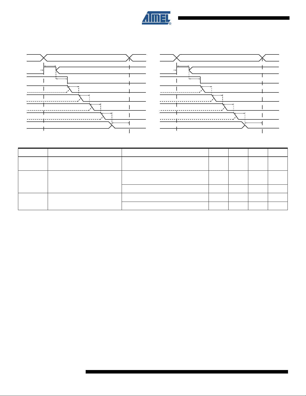
Figure 11-3. AT73C246 - RUN to POWERDOWN state Supplies Shutdown timing diagram.
RUN
STATE
SUPPLIES SHUTDOWN
POWEROFF
EVENT
POWERDOWN
STATE
T
PWRDOWN
T
OFF_AUDIO
T
OFF_VDD3
V
DD3
(3.3V)
V
DD1
(1.2V)
V
DD2
(1V)
3.3V
1.2V
1V
RSTB
V
DD0
(1.85V)
T
OFF_VDD1
T
OFF_VDD0
T
OFF_VDD2
V
DD4
(CODEC)
T
OFF_VDD4
1.85V
RUN
STATE
SUPPLIES SHUTDOWN
POWEROFF
EVENT
POWERDOWN
STATE
T
PWRDOWN
T
OFF_AUDIO
T
OFF_VDD2
V
DD2
(1V)
V
DD1
(1.2V)
V
DD3
(3.3V)
1V
1.2V
3.3V
RSTB
V
DD0
(1.85V)
T
OFF_VDD1
T
OFF_VDD0
T
OFF_VDD3
V
DD4
(CODEC)
T
OFF_VDD4
1.85V
SEQUENCE A SEQUENCE B
Table 11 - 2 . RUN to POWERDOWN state timing table
Symbol Parameter Comments Min Typ Max Units
T
PWRDOWN
POWERDOWN Event detection
time
Audio CODEC is OFF or Power Fail
T
OFF_AUDIO
Audio CODEC Shutdown Time
Occurs
Audio CODEC is ON 486 512 538 ms
VDDx is OFF in RUN state
T
OFF_VDDx
VDDx SHUTDOWN Time
VDDx is ON in RUN state
(1)
Note: 1. VDDx activity during RUN state is set by Bit7 of register VDDx_CTRL.
58 62 66 µs
58 62 66 µs
(1)
58 62 66 µs
4.8 5.2 5.4 ms
30
AT73C246
11050A–PMAAC–07-Apr-10
Page 31

When the POWERDOWN state is reached from the STANDBY state, the CPU power supplies
STANDBY
STATE
SUPPLIES SHUTDOWN
STANDBY_OUT
EVENT
POWERDOWN
STATE
T
STBY_OUT
T
OFF_VDD2
V
DD2
(1V)
V
DD0
(1.85V)
V
DD3
(3.3V)
1V
1.2V
RSTB
V
DD1
(1.2V)
T
OFF_VDD1
1.85V
T
OFF_VDD0
3.3V
T
OFF_VDD3
V
DD4
(CODEC)
T
OFF_VDD4
STANDBY
STATE
SUPPLIES SHUTDOWN
STANDBY_OUT
EVENT
POWERDOWN
STATE
T
STBY_OUT
T
OFF_VDD3
V
DD3
(3.3V)
V
DD0
(1.85V)
V
DD2
(1V)
3.3V
1.2V
RSTB
V
DD1
(1.2V)
T
OFF_VDD1
1.85V
T
OFF_VDD0
1V
T
OFF_VDD2
V
DD4
(CODEC)
T
OFF_VDD4
SEQUENCE A SEQUENCE B
are switched off sequentially as described in Figure 11-4.
Figure 11-4. AT73C246 - STANDBY to POWERDOWN state Supplies Shutdown timing diagram.
Table 11 - 3 . STANDBY to POWERDOWN state timing table
AT73C246
Symbol Parameter Comments Min Typ Max Units
T
STBY_OUT
T
OFF_VDDx
T
OFF_VDD4
STANDBY OUT Event
detection time
VDDx SHUTDOWN Time
VDD4 SHUTDOWN Time
VDDx is OFF during STANDBY state
VDDx is ON during STANDBY state
VDD4 is OFF in RUN state
VDD4 is ON in RUN state
(2)
(2)
(1)
(1)
95 100 105 µs
58 62 66 µs
4.8 5.2 5.4 ms
58 62 66 µs
4.8 5.2 5.4 ms
Notes: 1. VDDx activity during STANDBY state is set by register PMU_STANDBY_SUPPLIES.
2. VDD4 activity during RUN state is set by Bit7 of register VDD4_CTRL.
11.4.2 RUN STATE
When AT73C246 is in RUN state:
•VDD
{0,1,2,3,5}
power supplies are ON.
• RSTB pin is released.
• PMU functions are under software control (LDO4, AUDIO CODEC, ADC Controller)
• Led pin is driven according to register PMU_LED (0x0B).
11050A–PMAAC–07-Apr-10
31
Page 32

When RUN state is reached from the POWERDOWN state, the power supplies are sequentially
POWERDOWN
STATE
SUPPLIES START UP
T
ON_SYS
RUN STATE
VDD3 (3.3V)
T
ON_VDD3
VDD0 (1.85V)
T
ON_VDD0
VDD1 (1.2V)
TON_VDD1
VDD2 (1V)
3.3V
1.85V
1.2V
1V
T
ON_VDD2
RSTB
VPAD LEVEL
T
RESET
PWREN
EVENT
SEQUENCE A SEQUENCE B
POWERDOWN
STATE
SUPPLIES START UP
T
ON_SYS
RUN STATE
VDD2 (1V)
T
ON_VDD2
VDD0 (1.85V)
T
ON_VDD0
VDD1 (1.2V)
TON_VDD1
VDD3 (3.3V)
1V
1.85V
1.2V
3.3V
TON_VDD3
RSTB
VPAD LEVEL
T
RESET
PWREN
EVENT
started-up according to the Figure 11-5
Figure 11-5. AT73C246 - POWERDOWN to RUN state Supplies Start-Up timing diagram..
Table 11 - 4 . POWERDOWN to RUN state timing table
Symbol Parameter Comments Min Typ Max Units
T
ON_SYS
T
ON_VDD0
T
ON_VDD1
T
ON_VDD2
T
ON_VDD3
T
RESET
POWER-ON Event Detection Time 1.7 1.8 1.9 ms
VDD0 Start-up Time 5 5.3 5.6 ms
VDD1 Start-up Time 5 5.3 5.6 ms
VDD2 Start-up Time 5.2 5.5 5.8 ms
VDD3 Start-up Time 5.2 5.5 5.8 ms
All Regulators ON To RSTB High 30.4 32 33.6 ms
32
AT73C246
11050A–PMAAC–07-Apr-10
Page 33

When RUN state is reached from the STANDBY state, the power supplies are sequentially
SEQUENCE A SEQUENCE B
STANDBY
STAT E
SUPPLIES START UP
TON_SYS
RUN STATE
WAKEUP
EVENT
V
DD3
(3.3V)
TON_VDD3
TON_VDD0
TON_VDD1
V
DD2
(1V)
3.3V
1.85V
1.2V
1V
TON_VDD2
RSTB
VPAD LEVEL
TRESET
V
DD3
ON
or OFF
STANDBY
STAT E
SUPPLIES START UP
TON_SYS
RUN STATE
WAKEUP
EVENT
V
DD2
(1V)
TON_VDD2
TON_VDD0
TON_VDD1
V
DD3
(3.3V)
1V
1.85V
1.2V
3.3V
TON_VDD3
RSTB
VPAD LEVEL
TRESET
V
DD3
ON
or OFF
V
DD0
(1.85V)
V
DD1
(1.2V)
PFM
TPFM
PFM
V
DD0
(1.85V)
V
DD1
(1.2V)
PFM
TPFM
PFM
PWM
V
DD0
PWM
V
DD1
PWM
V
DD0
PWM
V
DD1
started-up according to the Figure 11-6.
Figure 11-6. AT73C246 - STANDBY to RUN state Supplies Start-Up timing diagram.
Table 11 - 5 . STANDBY to RUN state timing table
AT73C246
Symbol Parameter Comments Min Typ Max Units
T
ON_SYS
T
PFM
T
ON_VDDx
T
RESET
Start-up Time
PFM/PWM Switching
time
VDDx Start-up Time
All Regulators ON To
RSTB High
Time from validated WAKEUP event (end of debounce
time when applicable) to VDD2 or VDD3 power on.
Time from validated WAKEUP event (end of debounce
time when applicable) to PFM/PWM switching if
applicable.
VDDx is OFF during STANDBY state
VDDx is ON during STANDBY state
(1)
(1)
Note: 1. VDDx activity during STANDBY state is set by register PMU_STANDBY_SUPPLIES.
11.4.3 STANDBY STATE
When AT73C246 is in STANDBY state:
•V
BACKUP
•VDD
is ON.
are ON or OFF according to the status in register 0x03
{0,1,2,3}
(PMU_STANDBY_SUPPLIES)
•VDD
is ON or OFF according to the status in register 0x0A (VDD4_CTRL)
4
• Audio function is OFF
• ADC function is ON or OFF according to the status in register 0x30 (ADC_CTRL)
• RSTB pin is forced to ground.
• TWI pins are ignored to prevent TWI registers from corruption
• Led pin is driven according to register PMU_LED (0x0B)
To reach the STANDBY state, the appropriate power supplies are shut down as described in the
Figure 11-7 on page 34.
11050A–PMAAC–07-Apr-10
810 900 990 µs
420 470 520 µs
5.2 5.4 5.7 ms
58 62 66 µs
30.4 32 33.6 ms
33
Page 34

Figure 11-7. AT73C246 - RUN to STANDBY state Supplies Shutdown timing diagram.
RUN
STATE
SUPPLIES SHUTDOWN
STANDBY
EVENT
STANDBY
STATE
T
STANDBY
T
OFF_AUDIO
T
OFF_VDD2
T
WAIT +
V
DD2
(1V)
V
DD3
(3.3V)
1V
1.2V
1.85V
3.3V
RSTB
T
OFF_VDD1
T
OFF_VDD0
T
OFF_VDD3
1.85V
(V
DD3
ON
or OFF
)
SEQUENCE A SEQUENCE B
RUN
STAT E
SUPPLIES SHUTDOWN
STANDBY
EVENT
STANDBY
STATE
T
STANDBY
T
OFF_AUDIO
T
OFF_VDD3
T
WAIT +
V
DD3
(3.3V)
V
DD2
(1V)
3.3V
1.2V
1.85V
1V
RSTB
T
OFF_VDD1
T
OFF_VDD0
T
OFF_VDD2
1.85V
(V
DD3
ON
or OFF
)
V
DD1
(1.2V)
V
DD0
(1.85V)
TPWM
PWM
PWM
V
DD1
(1.2V)
V
DD0
(1.85V)
TPWM
PWM
PWM
PFM
V
DD0
PFM
V
DD1
PFM
V
DD0
PFM
V
DD1
Table 11 - 6 . RUN to STANDBY state timing table
Symbol Parameter Comments Min Typ Max Units
T
STANDBY
T
PWM
T
WAIT
T
OFF_AUDIO
T
OFF_VDDx
T
ON_VDDx
STANDBY Event
Detection Time
PFM/PWM Switching
time
WAKEUP Event
Detection Window
Audio CODEC
Shutdown Time
VDDx SHUTDOWN
Time
VDDx STARTUP Time
Time from validated WAKEUP event (end of debounce
time when applicable) to PFM/PWM switching if
applicable.
If a WAKEUP event occurs in this window the PMU
automatically restart at the end of the STANDBY
process.
Audio CODEC is ON 486 512 538 ms
Audio CODEC is OFF 58 62 66 µs
VDDx is OFF during both STANBY
VDDx is OFF during STANBY state
VDDx is ON during RUN state
(2)
.
VDDx is ON during STANBY state
VDDx is OFF during RUN state
(2)
.
VDDx is ON during both STANBY
(1)
and RUN
(1)
.
(1)
.
(1)
and RUN
(2)
states. 58 62 66 µs
(2)
states. 58 62 66 µs
Note: 1. VDDx activity during STANDBY state is set by register PMU_STANDBY_SUPPLIES.
2. VDDx activity during RUN state is set by Bit7 of register VDDx_CTRL.
11.4.4 HRST STATE
HRST state is a transition state used to restart the CPU:
150 160 170 µs
460 500 540 µs
150 160 170 µs
4.8 5.2 5.4 ms
4.8 5.2 5.4 ms
34
•VDD
{0,1,2,3,4}
are switched off according to figure Figure 11-8 on page 35 depending on the
previous state
AT73C246
•VDD
• RSTB pin is forced to ground
is ON
5
11050A–PMAAC–07-Apr-10
Page 35

AT73C246
RUN / STANDBY /
POWERDOWN
STAT E
SUPPLIES SHUTDOWN
HRST_EVENT
EVENT
HRST
STATE
T
HRST
T
OFF_VDD3
T
OFF_AUDIO
V
DD3
(3.3V)
V
DD1
(1.2V)
V
DD2
(1V)
3.3V
1.2V
1.85V
1V
RSTB
V
DD0
(1.85V)
T
OFF_VDD1
T
OFF_VDD0
T
OFF_VDD2
PMU FUNCTIONS
(LDO4, ADC, LED,...)
T
OFF_PMU
RUN / STANDBY /
POWERDOWN
STATE
SUPPLIES SHUTDOWN
HRST_EVENT
EVENT
HRST
STATE
T
HRST
T
OFF_VDD2
T
OFF_AUDIO
V
DD2
(1V)
V
DD1
(1.2V)
V
DD3
(3.3V)
1V
1.2V
1.85V
3.3V
RSTB
V
DD0
(1.85V)
T
OFF_VDD1
T
OFF_VDD0
T
OFF_VDD3
PMU FUNCTIONS
(LDO4, ADC, LED,...)
T
OFF_PMU
SEQUENCE A SEQUENCE B
Figure 11-8. AT73C246 - HRST state Supplies Shutdown timing diagram.
Table 11 - 7 . HRST state timing table from RUN STATE
Symbol Parameter Comments Min Typ Max Units
T
HRST
T
OFF_AUDIO
T
OFF_VDDx
T
OFF_PMU
HRST Event Detection Time 58 62 66 µs
Audio CODEC is ON 486 512 538 ms
Audio CODEC Shutdown Time
Audio CODEC is OFF 58 62 66 µs
VDDx SHUTDOWN Time
VDDx is OFF in RUN state
VDDx is ON in RUN state
(1)
(1)
58 62 66 µs
4.8 5.2 5.4 ms
PMU Functions Shutdown Time 1.4 1.5 1.6 ms
Note: 1. VDDx activity during RUN state is set by Bit7 of register VDDx_CTRL
Table 11 - 8 . HRST state timing table from STANDBY STATE
Symbol Parameter Comments Min Typ Max Units
T
HRST
T
OFF_AUDIO
T
OFF_VDDx
T
OFF_VDD4
T
OFF_PMU
Notes: 1. VDDx activity during STANDBY state is set by register PMU_STANDBY_SUPPLIES.
11050A–PMAAC–07-Apr-10
HRST Event Detection
Time
Audio CODEC Shutdown
Time
VDDx SHUTDOWN Time
VDD4 SHUTDOWN Time
Audio CODEC is ON 486 512 538 ms
Audio CODEC is OFF 58 62 66 µs
VDDx is OFF during STANDBY state
VDDx is ON during STANDBY state
VDD4 is OFF in RUN state
VDD4 is ON in RUN state
(2)
(2)
(1)
(1)
PMU Functions Shutdown
Time
2. VDD4 activity during RUN state is set by Bit7 of register VDD4_CTRL.
58 62 66 µs
58 62 66 µs
4.8 5.2 5.4 ms
58 62 66 µs
4.8 5.2 5.4 ms
1.4 1.5 1.6 ms
35
Page 36

11.5 DCDC0 and DCDC1 Functional Description
DCDC0 and DCDC1 are 2 identical high performance synchronous step-down (buck) converters. They feature:
• 2 control modes: PFM and PWM,
• A soft start circuit,
• A software programmable output voltage between 0.8 and 3.6V with automatic ramping for
DVS application,
• An Over-Current-Protection circuit,
• A 180 degree out of phase operating mode.
11.5.1 PFM and PWM Control Modes
Pulse Frequency Modulation control is an hysteretic control of the output voltage. It is specially
intended for light loads (< 50mA typ). In this mode, the DCDC converter exhibits a very low quiescent current (< 50
operation in this mode is not fixed but proportional to the load current.
Pulse Width Modulation control is a fixed frequency, variable duty cycle control of the DCDC
converter. It has a fast and precise feedback loop specially intended to handle hard loads and
low output ripple voltage.
At start-up, DCDC0 and DCDC1 operate in PWM mode. This way, high load at CPU boot are
properly handled. Through software control in registers VDD0_CTRL (0x06) and VDD1_CTRL
(0x07), the user may enter the low-power mode (PFM) when the application consumption is
reduced.
µA) thus achieving very high efficiency at light loads. The frequency of
11.5.2 Soft-start Circuit
DCDC0 and DCDC1 feature a soft start circuit to prevent high input current while charging the
output capacitor from 0V to the default output voltage. Typically, the in-rush current at start-up
(with no load) is limited to 30 mA.
11.5.3 Output Voltage Programming
DCDC0 and DCDC1 output voltages can be managed through software control in registers
VDD0_CTRL (0x06) and VDD1_CTRL (0x07). 50mV steps are provided from 0.8V to 3.6V. It is
recommended to use the automatic ramping function in register PMU_SUPPLY_CTRL (0x04) to
achieve smooth operation. When the DVS_VDD
are ramped from the current value to the final value in 50mV / 280us steps. For users who intend
to disable the DVS_VDD
At power up, DCDC0 and DCDC1 default output voltages are respectively 1.85V and 1.20V. For
different default output voltages, please contact Atmel.
11.5.4 180
° Out-of-phase Operation
DCDC0 and DCDC1 can be operated in-phase or at 180
tion bit in register PMU_SUPPLY_CTRL (0x04). When operated in phase both converters will
start charging their inductor at the same time. When operated at 180
charge start time will be shifted by half a 2MHz clock delay (= 250ns) from one converter to the
other. This latter scheme tends to average the input current of both DCDC converters.
bit is active (default mode), output voltages
{0,1}
bit, a maximum of 4 steps (= 200mV) per 100us is allowed.
{0,1}
° out-of-phase according to the selec-
° out-of-phase, the inductor
36
AT73C246
11050A–PMAAC–07-Apr-10
Page 37

11.6 LDO2 Functional Description
LDO2 is a linear voltage regulator intended to supply CPU core voltages in the range 0.8V to
1.35V. Its maximum input voltage is 3.6V. Thus, it must not be wired to the VIN plane with VINSYS, VIN0, VIN1, VIN3 and VIN4 if VIN is above 3.6V. Considering its low-output voltage and
for the sake of efficiency and power dissipation, the user may connect it at the output of DCDC0.
This LDO features:
• A soft start circuit,
• A software programmable output voltage between 0.8 and 1.35V with automatic ramping for
DVS application.
11.6.1 Soft-start Circuit
LDO2 features a soft start circuit to prevent high input current while charging the output capacitor from 0V to the default output voltage. This soft start circuit limits the input current during 5ms
(+/-5%) at startup to 200mA in typical conditions. After this delay, LDO2 recovers full current
capability.
11.6.2 Output Voltage Programming
LDO2 output voltage can be managed through software control in register VDD2_CTRL (0x08).
50mV steps are provided from 0.8V to 1.35V. It is recommended to use the automatic ramping
function in register PMU_SUPPLY_CTRL (0x04) to achieve smooth operation. When the
DVS_VDD2 bit is active (default mode), output voltages are ramped from the current value to
the final value in 50mV / 600us steps.
AT73C246
At power up, LDO2 default output voltage is 1V. For different default output voltage, please contact Atmel.
11.7 LDO3 and LDO4 Functional Description
LDO3 and LDO4 are low dropout linear voltage regulators intended to supply CPU peripherals
(I/Os, analog functions) in the range 2.7V to 3.6V. They can be operated directly from a 5.5V
maximum input voltage. They feature:
• A soft start circuit,
• A software programmable output between 2.7V and 3.6V voltage with automatic ramping for
DVS application,
11.7.1 Soft-start Circuit
LDO3 and LDO4 feature a soft start circuit to prevent high input current while charging the output capacitor from 0V to the default output voltage. This soft start circuit limits the input current
during 5ms (+/-5%) at startup to 200mA in typical conditions. After this delay, LDO3(4) recovers
full current capability.
11.7.2 Output Voltage Programming
LDO3 and LDO4 output voltages can be managed through software control in registers
VDD3_CTRL (0x09) and VDD4_CTRL (0x0A). 50mV steps are provided from 2.7V to 3.6V. It is
recommended to use the automatic ramping function in register PMU_SUPPLY_CTRL (0x04) to
achieve smooth operation. When the DVS_VDD
are ramped from the current value to the final value in 50mV / 600us steps.
bit is active (default mode), output voltages
{3,4}
11050A–PMAAC–07-Apr-10
37
Page 38

At power up, LDO3 an LDO4 default output voltages are both 3.3V. For different default output
voltages, please contact Atmel.
11.8 Power Fail Detectors
AT73C246 features a Power Fail detector on each CPU supplies (V
function is made of a comparator that toggles each time one the listed power supplies goes
below a defined threshold. The comparator toggling is considered by the PMU digital state
machine as a POWER-FAIL event.
The threshold value of the power fail detector is proportional to the output voltage of the regulator. It is not a fixed voltage, it is adapted to the programmed output voltage. The default
threshold value is set according to register PMU_RST_LVL (0x05) and can be programmed to
another value through TWI access. For other default threshold values at startup, please contact
Atmel.
11.9 Measurement Bridge and 10-bit ADC
AT73C246 features a 10-channel measurement chain including:
• A multiplexer + attenuator followed by a unity gain buffer
• A 300kS/s 10-bit SAR ADC.
ADC function is enabled through the register ADC_CTRL (0x30). ADC_MUX_1 (0x31) and
ADC_MUX_2 (0x32) allow the selection of inputs to be measured. 1 to 10 inputs can be
selected. The ADC will then perform serial conversion on these inputs and write the corresponding result in registers 0x33 to 0x49.
DD0
, V
DD1
, V
DD2
, V
DD3
). This
2 sampling modes are provided to perform periodic conversions:
• Max speed
• Low speed.
To enter these modes, refer to the sampling period bits (TS) in the register ADC_CTRL (0x30).
When MAX_SPEED mode is selected, the ADC runs at 300kS/s and loop without any dead time
over the selected inputs. When a LOW_SPEED sampling period is selected, the ADC performs
a set of input conversions (1 to 10) at 300kS/s and then wait for one sampling period (defined by
TS bits) to start another set of conversions.
38
AT73C246
11050A–PMAAC–07-Apr-10
Page 39

Figure 11-9. Measurement Bridge and 10-bit ADC Block Diagram.
VREFP
ADC
V
INSYS
VDD0
VDD1
VDD2
VDD3
VDD4
ANA0
ANA1
ANA2
ANA3
ADC_ANA0_MSB
ADC_ANA0_LSB
ADC_ANA_LSB
0
0
0
TWI Registers
ADCOUT <9:0>
VREFN
VDDC
VREFP
GNDSYS
BUFFER
0x30
ADC_CTRL
0x31
ADC_MUX_1
0x32
ADC_MUX_2
MUX
10 1
10-channel
resistive attenuator
AT73C246
11050A–PMAAC–07-Apr-10
39
Page 40

11.10 Real Time Clock (RTC) User Interface
RTC ADDR
RTC DATA 3 RTC DATA 2 RTC DATA 1 RTC DATA 0
CONTROL REGISTER
STAT US CLEAR COMMAND REGISTER
MODE REGISTER
TIME REGISTER
CALENDAR REGISTER
TIME ALARM REGISTER
CALENDAR ALARM REGISTER
STAT US REGISTER
INTERRUPT ENABLE REGISTER
INTERRUPT DISABLE REGISTER
INTERRUPT MASK REGISTER
VALID ENTRY REGISTER
VERSION REGISTER
RESERVED REGISTER
RTC
CTRL
RTC_SEL
RTC_EN
RTC_WRITE
RTC
Figure 11-10. RTC Block Diagram
Table 11 - 9 . Register Mapping
Offset Register Name Access Reset
0x00 Control Register RTC_CR Read-write 0x0
0x04 Mode Register RTC_MR Read-write 0x0
0x08 Time Register RTC_TIMR Read-write 0x0
0x0C Calendar Register RTC_CALR Read-write 0x01819819
0x10 Time Alarm Register RTC_TIMALR Read-write 0x0
0x14 Calendar Alarm Register RTC_CALALR Read-write 0x01010000
0x18 Status Register RTC_SR Read-only 0x0
0x1C Status Clear Command Register RTC_SCCR Write-only ---
0x20 Interrupt Enable Register RTC_IER Write-only ---
0x24 Interrupt Disable Register RTC_IDR Write-only ---
0x28 Interrupt Mask Register RTC_IMR Read-only 0x0
0x2C Valid Entry Register RTC_VER Read-only 0x0
0xFC Version Register
0xFC Reserved Register --- --- ---
Note: 1. Values in the Version Register vary with the version of the IP block implementation.
40
AT73C246
(1)
RTC_VERSION Read-only ---
11050A–PMAAC–07-Apr-10
Page 41

11.10.1 RTC Register Read/Write Operation
RTC_EN
RTC_SEL
RTC_WRITE
RTC_DATA
RTC_ADDR
WRITE
RTC_ADDR
READ
RTC_DATA3
READ
RTC_DATA2
READ
RTC_DATA1
READ
RTC_DATA0
WRITE 02
@RTC_CTRL
WRITE 03
@RTC_CTRL
WRITE 02
@RTC_CTRL
WRITE 00
@RTC_CTRL
RTC_EN = 0
RTC_SEL = 1
RTC_WRITE = 0
RTC_EN = 1
RTC_SEL = 1
RTC_WRITE = 0
RTC_EN = 0
RTC_SEL = 1
RTC_WRITE = 0
RTC_EN = 0
RTC_SEL = 0
RTC_WRITE = 0
TWI ACCESS
RTC_EN
RTC_SEL
RTC_WRITE
RTC_DATA
RTC_ADDR
WRITE
RTC_ADDR
WRITE
RTC_DATA3
WRITE
RTC_DATA2
WRITE
RTC_DATA1
WRITE
RTC_DATA0
WRITE 06
@RTC_CTRL
WRITE 07
@RTC_CTRL
WRITE 06
@RTC_CTRL
WRITE 00
@RTC_CTRL
RTC_EN = 0
RTC_SEL = 1
RTC_WRITE = 1
RTC_EN = 1
RTC_SEL = 1
RTC_WRITE = 1
RTC_EN = 0
RTC_SEL = 1
RTC_WRITE = 1
RTC_EN = 0
RTC_SEL = 0
RTC_WRITE = 0
TWI ACCESS
Figure 11-11. RTC Read Operation
AT73C246
Figure 11-12. RTC Write Operation
41
11050A–PMAAC–07-Apr-10
Page 42

11.10.2 RTC Control Register
Name: RTC_CR
Access: Read-write
Address: 0x00
31 30 29 28 27 26 25 24
––––––––
23 22 21 20 19 18 17 16
–––––– CALEVSEL
15 14 13 12 11 10 9 8
–––––– TIMEVSEL
76543210
––––––UPDCALUPDTIM
• UPDTIM: Update Request Time Register
0 = No effect.
1 = Stops the RTC time counting.
Time counting consists of second, minute and hour counters. Time counters can be programmed once this bit is set and
acknowledged by the bit ACKUPD of the Status Register.
• UPDCAL: Update Request Calendar Register
0 = No effect.
1 = Stops the RTC calendar counting.
Calendar counting consists of day, date, month, year and century counters. Calendar counters can be programmed once
this bit is set.
• TIMEVSEL: Time Event Selection
The event that generates the flag TIMEV in RTC_SR (Status Register) depends on the value of TIMEVSEL.
0 = Minute change.
1 = Hour change.
2 = Every day at midnight.
3 = Every day at noon.
• CALEVSEL: Calendar Event Selection
The event that generates the flag CALEV in RTC_SR depends on the value of CALEVSEL.
0 = Week change (every Monday at time 00:00:00).
1 = Month change (every 01 of each month at time 00:00:00).
2, 3 = Year change (every January 1 at time 00:00:00)
42
AT73C246
11050A–PMAAC–07-Apr-10
Page 43

11.10.3 RTC Mode Register
Name: RTC_MR
Access: Read-write
Address: 0x04
31 30 29 28 27 26 25 24
––––––––
23 22 21 20 19 18 17 16
––––––––
15 14 13 12 11 10 9 8
––––––––
76543210
–––––––HRMOD
• HRMOD: 12-/24-hour Mode
0 = 24-hour mode is selected.
1 = 12-hour mode is selected.
All non-significant bits read zero.
AT73C246
11050A–PMAAC–07-Apr-10
43
Page 44

11.10.4 RTC Time Register
Name: RTC_TIMR
Access: Read-write
Address: 0x08
31 30 29 28 27 26 25 24
––––––––
23 22 21 20 19 18 17 16
–AMPM HOUR
15 14 13 12 11 10 9 8
–MIN
76543210
–SEC
• SEC: Current Second
The range that can be set is 0 - 59 (BCD).
The lowest four bits encode the units. The higher bits encode the tens.
• MIN: Current Minute
The range that can be set is 0 - 59 (BCD).
The lowest four bits encode the units. The higher bits encode the tens.
• HOUR: Current Hour
The range that can be set is 1 - 12 (BCD) in 12-hour mode or 0 - 23 (BCD) in 24-hour mode.
• AMPM: Ante Meridiem Post Meridiem Indicator
This bit is the AM/PM indicator in 12-hour mode.
0 = AM.
1 = PM.
All non-significant bits read zero.
44
AT73C246
11050A–PMAAC–07-Apr-10
Page 45

11.10.5 RTC Calendar Register
Name: RTC_CALR
Access: Read-write
Address: 0x0C
31 30 29 28 27 26 25 24
–– DATE
23 22 21 20 19 18 17 16
DAY MONTH
15 14 13 12 11 10 9 8
YEAR
76543210
–CENT
•CENT: Current Century
The range that can be set is 19 - 20 (BCD).
The lowest four bits encode the units. The higher bits encode the tens.
• YEAR: Current Year
The range that can be set is 00 - 99 (BCD).
The lowest four bits encode the units. The higher bits encode the tens.
AT73C246
• MONTH: Current Month
The range that can be set is 01 - 12 (BCD).
The lowest four bits encode the units. The higher bits encode the tens.
• DAY: Current Day
The range that can be set is 1 - 7 (BCD).
The coding of the number (which number represents which day) is user-defined as it has no effect on the date counter.
• DATE: Current Date
The range that can be set is 01 - 31 (BCD).
The lowest four bits encode the units. The higher bits encode the tens.
All non-significant bits read zero.
11050A–PMAAC–07-Apr-10
45
Page 46

11.10.6 RTC Time Alarm Register
Name: RTC_TIMALR
Access: Read-write
Address: 0x10
31 30 29 28 27 26 25 24
––––––––
23 22 21 20 19 18 17 16
HOUREN AMPM HOUR
15 14 13 12 11 10 9 8
MINEN MIN
76543210
SECEN SEC
• SEC: Second Alarm
This field is the alarm field corresponding to the BCD-coded second counter.
• SECEN: Second Alarm Enable
0 = The second-matching alarm is disabled.
1 = The second-matching alarm is enabled.
• MIN: Minute Alarm
This field is the alarm field corresponding to the BCD-coded minute counter.
• MINEN: Minute Alarm Enable
0 = The minute-matching alarm is disabled.
1 = The minute-matching alarm is enabled.
• HOUR: Hour Alarm
This field is the alarm field corresponding to the BCD-coded hour counter.
• AMPM: AM/PM Indicator
This field is the alarm field corresponding to the BCD-coded hour counter.
• HOUREN: Hour Alarm Enable
0 = The hour-matching alarm is disabled.
1 = The hour-matching alarm is enabled.
46
AT73C246
11050A–PMAAC–07-Apr-10
Page 47

11.10.7 RTC Calendar Alarm Register
Name: RTC_CALALR
Access: Read-write
Address: 0x14
31 30 29 28 27 26 25 24
DATEEN – DATE
23 22 21 20 19 18 17 16
MTHEN – – MONTH
15 14 13 12 11 10 9 8
––––––––
76543210
––––––––
• MONTH: Month Alarm
This field is the alarm field corresponding to the BCD-coded month counter.
• MTHEN: Month Alarm Enable
0 = The month-matching alarm is disabled.
1 = The month-matching alarm is enabled.
AT73C246
• DATE: Date Alarm
This field is the alarm field corresponding to the BCD-coded date counter.
• DATEEN: Date Alarm Enable
0 = The date-matching alarm is disabled.
1 = The date-matching alarm is enabled.
11050A–PMAAC–07-Apr-10
47
Page 48

11.10.8 RTC Status Register
Name: RTC_SR
Access: Read-only
Address: 0x18
31 30 29 28 27 26 25 24
––––––––
23 22 21 20 19 18 17 16
––––––––
15 14 13 12 11 10 9 8
––––––––
76543210
– – – CALEV TIMEV SEC ALARM ACKUPD
• ACKUPD: Acknowledge for Update
0 = Time and calendar registers cannot be updated.
1 = Time and calendar registers can be updated.
• ALARM: Alarm Flag
0 = No alarm matching condition occurred.
1 = An alarm matching condition has occurred.
• SEC: Second Event
0 = No second event has occurred since the last clear.
1 = At least one second event has occurred since the last clear.
• TIMEV: Time Event
0 = No time event has occurred since the last clear.
1 = At least one time event has occurred since the last clear.
The time event is selected in the TIMEVSEL field in RTC_CTRL (Control Register) and can be any one of the following
events: minute change, hour change, noon, midnight (day change).
• CALEV: Calendar Event
0 = No calendar event has occurred since the last clear.
1 = At least one calendar event has occurred since the last clear.
The calendar event is selected in the CALEVSEL field in RTC_CR and can be any one of the following events: week
change, month change and year change.
48
AT73C246
11050A–PMAAC–07-Apr-10
Page 49

11.10.9 RTC Status Clear Command Register
Name: RTC_SCCR
Access: Write-only
Address: 0x1C
31 30 29 28 27 26 25 24
––––––––
23 22 21 20 19 18 17 16
––––––––
15 14 13 12 11 10 9 8
––––––––
76543210
– – – CALCLR TIMCLR SECCLR ALRCLR ACKCLR
• ACKCLR: Acknowledge Clear
0 = No effect.
1 = Clears corresponding status flag in the Status Register (RTC_SR).
• ALRCLR: Alarm Clear
0 = No effect.
1 = Clears corresponding status flag in the Status Register (RTC_SR).
AT73C246
• SECCLR: Second Clear
0 = No effect.
1 = Clears corresponding status flag in the Status Register (RTC_SR).
• TIMCLR: Time Clear
0 = No effect.
1 = Clears corresponding status flag in the Status Register (RTC_SR).
• CALCLR: Calendar Clear
0 = No effect.
1 = Clears corresponding status flag in the Status Register (RTC_SR).
11050A–PMAAC–07-Apr-10
49
Page 50

11.10.10 RTC Interrupt Enable Register
Name: RTC_IER
Access: Write-only
Address: 0x20
31 30 29 28 27 26 25 24
––––––––
23 22 21 20 19 18 17 16
––––––––
15 14 13 12 11 10 9 8
––––––––
76543210
– – – CALEN TIMEN SECEN ALREN ACKEN
• ACKEN: Acknowledge Update Interrupt Enable
0 = No effect.
1 = The acknowledge for update interrupt is enabled.
• ALREN: Alarm Interrupt Enable
0 = No effect.
1 = The alarm interrupt is enabled.
• SECEN: Second Event Interrupt Enable
0 = No effect.
1 = The second periodic interrupt is enabled.
• TIMEN: Time Event Interrupt Enable
0 = No effect.
1 = The selected time event interrupt is enabled.
• CALEN: Calendar Event Interrupt Enable
0 = No effect.
• 1 = The selected calendar event interrupt is enabled.
50
AT73C246
11050A–PMAAC–07-Apr-10
Page 51

11.10.11 RTC Interrupt Disable Register
Name: RTC_IDR
Access: Write-only
Address: 0x24
31 30 29 28 27 26 25 24
––––––––
23 22 21 20 19 18 17 16
––––––––
15 14 13 12 11 10 9 8
––––––––
76543210
– – – CALDIS TIMDIS SECDIS ALRDIS ACKDIS
• ACKDIS: Acknowledge Update Interrupt Disable
0 = No effect.
1 = The acknowledge for update interrupt is disabled.
• ALRDIS: Alarm Interrupt Disable
0 = No effect.
1 = The alarm interrupt is disabled.
AT73C246
• SECDIS: Second Event Interrupt Disable
0 = No effect.
1 = The second periodic interrupt is disabled.
• TIMDIS: Time Event Interrupt Disable
0 = No effect.
1 = The selected time event interrupt is disabled.
• CALDIS: Calendar Event Interrupt Disable
0 = No effect.
1 = The selected calendar event interrupt is disabled.
11050A–PMAAC–07-Apr-10
51
Page 52

11.10.12 RTC Interrupt Mask Register
Name: RTC_IMR
Access: Read-only
Address: 0x28
31 30 29 28 27 26 25 24
––––––––
23 22 21 20 19 18 17 16
––––––––
15 14 13 12 11 10 9 8
––––––––
76543210
– – – CAL TIM SEC ALR ACK
• ACK: Acknowledge Update Interrupt Mask
0 = The acknowledge for update interrupt is disabled.
1 = The acknowledge for update interrupt is enabled.
• ALR: Alarm Interrupt Mask
0 = The alarm interrupt is disabled.
1 = The alarm interrupt is enabled.
• SEC: Second Event Interrupt Mask
0 = The second periodic interrupt is disabled.
1 = The second periodic interrupt is enabled.
• TIM: Time Event Interrupt Mask
0 = The selected time event interrupt is disabled.
1 = The selected time event interrupt is enabled.
• CAL: Calendar Event Interrupt Mask
0 = The selected calendar event interrupt is disabled.
1 = The selected calendar event interrupt is enabled.
52
AT73C246
11050A–PMAAC–07-Apr-10
Page 53
11.10.13 RTC Valid Entry Register
Name: RTC_VER
Access: Read-only
Address: 0x2C
31 30 29 28 27 26 25 24
––––––––
23 22 21 20 19 18 17 16
––––––––
15 14 13 12 11 10 9 8
––––––––
76543210
––––NVCALALRNVTIMALRNVCALNVTIM
• NVTIM: Non-valid Time
0 = No invalid data has been detected in RTC_TIMR (Time Register).
1 = RTC_TIMR has contained invalid data since it was last programmed.
• NVCAL: Non-valid Calendar
0 = No invalid data has been detected in RTC_CALR (Calendar Register).
1 = RTC_CALR has contained invalid data since it was last programmed.
AT73C246
• NVTIMALR: Non-valid Time Alarm
0 = No invalid data has been detected in RTC_TIMALR (Time Alarm Register).
1 = RTC_TIMALR has contained invalid data since it was last programmed.
• NVCALALR: Non-valid Calendar Alarm
0 = No invalid data has been detected in RTC_CALALR (Calendar Alarm Register).
1 = RTC_CALALR has contained invalid data since it was last programmed.
11050A–PMAAC–07-Apr-10
53
Page 54

11.10.14 RTC Version register
Name: RTC_VERSION
Access: Read-only
Address: 0xFC
31 30 29 28 27 26 25 24
––––––––
23 22 21 20 19 18 17 16
––––– MFN
15 14 13 12 11 10 9 8
–––– VERSION
76543210
VERSION
• VERSION
Reserved. Value subject to change. No funcionality associated. This is the Atmel internal version of the macrocell.
•MFN
Reserved. Value subject to change. No funcionality associated.
11.11 Die Temperature Sensor
The AT73C246 features a die temperature sensor for protection reasons. If the junction temperature rises above the shutdown threshold for a minimum time of 1ms (+/- 5%), the power
manager event T
restart threshold for more than 1ms, the power manager event T
The two internal thresholds shutdown and restart are defined in Section 9.11 “Die Temperature
Sensor” on page 21.
> 130°C is asserted. In a similar fashion, if the temperature falls through the
J
<110°C is asserted.
J
54
AT73C246
11050A–PMAAC–07-Apr-10
Page 55

12. Audio Codec Functional Description
MUX
ADC DAC
DSP
+
Audio
Controller
BYPASS
0 -> -30dB
-77/+6dB
VMID
-34 -> +12dB
0 -> +46dB
LINL
AUXL
MICL
MICLN
MICBIAS AVDD
200K
VMID AGND
HPDET
Codec Bias
MCLKBCLKLRFSDAIPAO
I²S
HPVCM
HPL
MUX
ADC DAC
BYPASS
0 -> -30dB
-77/+6dB
-34 -> +12dB
LINR
AUXR
HPR
200K
2K
1dB Step
1dB Step
1dB Step
1dB Step
1dB Step
1dB Step
1dB Step
0 -> +46dB
MICR
MICRN
1dB Step
12.1 Description
AT73C246 features a high quality, low power stereo audio codec with integrated headphone
amplifier.
AT73C246
The playback channel accommodates 16 to 24-bit stereo programmable format entering the digital audio interface (I
Sigma Delta Stereo DAC. An output mixer allows to mix this DAC output with a line / aux or
microphone input.
A 16-32 Ohms Stereo headphone amplifier with virtual ground output provides a 97dB SNR output for line / headphone loads. The virtual ground output allows to remove 2 space demanding
coupling capacitors on board.
On the record side, a multiplexer can select between a main stereo line input and a stereo auxiliary input such as an FM radio. A stereo microphone input with up to 46dB gain is provided. A
stereo input mixer allows mixing between line (or aux) and microphone channels before entering
a 96dB SNR Stereo Sigma Delta ADC. The digital audio signal is then digitally filtered and transferred to the I
2
S audio interface.
12.2 Audio Codec Block Diagram
Figure 12-1. Audio Codec Block Diagram
2
S) and delivers an internal analog audio output through a 100dB SNR
11050A–PMAAC–07-Apr-10
55
Page 56

12.3 Audio Codec Controls
BCLKINV
ENASR
STDBY
ENAC
LINBOTH
RINBOTH
DAIMODE
MCLKSEL
SELFS
RHSBOTH
LHSBOTH
I2S INTERFACE
MASTER
SSCMODE
WL
ASRTIME
PATHSEL
AUDIO
C ONTR OLLE R
ADCL
DACL
ADCR
Digital
Processor
DACR
GSDT
Sidetone
-30 to +0dB
LINESEL
ONLINR
ONADCR
ONADCL
ONDACL
ONDACR
MONODAC
MONOADC
-35 to +12dB
Gain Control
1dB step
3dB step
+
+
DEEMP
DEEMP
0 to +46dB
1dB step
ONMICR
MICRVOL
INRVOL
MIXLINER
+
ONMIXR
MIXMICR
-35 to 12dB
1dB step
0 to +46dB
1dB step
ONLINL
ONMICL
Gain Control
INLVOL
MICLVOL
LINESEL
MIXMICL
+
ONMIXL
MIXLINEL
ONPLAYBACK
ONPLAYBACK
HPL
HPR
HPVCM
MUTEMICL
MUTEINL
MICLDIFF
MICRDIFF
EQUALIZER
MUTEDACL
SWAPDAC
SWAPADC
EQUALIZER
MUTEDACR
MUTEHPL
-77 to 6dB
1dB step
MUTEHPR
HPRVOL
DCBLOCK
ONHPR
HPDET
ONHPL/R
GSDT
Sidetone
-30 to +0dB
ONSIDETONE
ONBYPASS
ONSIDETONE
ONBYPASS
3dB step
FX3D
FX3D
-77 to 6dB
1dB step
MUTEINR
MICL
MICLN
LINEINL
AUXI NL
MICR
MICRN
LINEINR
AUXI NR
MUTEMICR
DCBLOCK
ONHPL
ONMICBIAS
MICDETLEV
VMIDAVD DMICBIAS AGND
TWI
DCBLOCK
VMID
HPLVOL
2K 200K 200K
ONMICBIAS
Figure 12-2. Audio Codec Controls
56
AT73C246
11050A–PMAAC–07-Apr-10
Page 57

12.4 Audio Controller
The audio controller sequences the power-up and power-down of the audio codec sub-functions
(Mic.amp / ADC / DAC / …). During these transitioning phases, the controller also manages the
gain steps to fade them in and out, thus providing smooth operation.
Depending on the application, two modes are provided:
Dedicated to the major audio path scenarios (those described in Table 13-25 on page 95), this
mode enables the whole audio path setup only via "PATHSEL" bits in register AUTOSTART
(0x10).
Dedicated to audio path scenarios not described in the previously mentioned table, this mode
brings the flexibility to start manually the audio sub-functions.
The following figure shows the global context of the audio codec control.
Figure 12-3. Audio Codec Typical Control Sequence
AT73C246
1. Automatic path control
2. Custom path control
Apply Supply
1
& MCLK
Configure
Analog & Digital
2
Interfaces
Unmute Codec
3
Start Audio
Codec in
4
Standby
5
Software
Wait
Registers to set :
- AUDIO_CONTROL (0x11)
(Set DCBlock bit here)
- MIC_CONTROL (0x12)
- DAI_CONTROL (0x13)
- FRAME_CONTROL (0x14)
Register to set :
- MUTE (0x15)
Register to set :
- AUTOSTART (0x10)
Typically 350ms.
- See VMID section.
Automatic path
control
Shutdown
7
Audio Codec
Software
Wait
Unset
9
DCBLOCK bit
Remove MCLK
10
& supply
6
8
Custom path
control
Register to set :
- AUTOSTART (0x10)
At least 1s.
- See “Power-off Time”
section.
Register to set :
- AUDIO_CONTROL (0x11)
- See “AC/DC coupled load
management” section.
Registers to set
- See dedicated sections.
11050A–PMAAC–07-Apr-10
57
Page 58

12.4.1 Audio Codec General Recommendations
12.4.1.1 V
MID
•V
is the common mode voltage of the audio codec analog core. It is recommended to
MID
decouple this voltage with a 1uF capacitor to ensure low noise operation as well as slow
(thus silent) transients at codec power up and power down.
•The V
capacitor is charged and discharged whenever the ENAC bit is set or cleared.
MID
Particularly, placing the audio codec in STANDBY mode does not discharge the V
capacitor. The software WAIT operations in the previous diagram (step #5 and step #8 in
“Audio Codec Typical Control Sequence” on page 57) should accommodate V
time constant. See “Audio Codec Bias” on page 22..
12.4.1.2 AC / DC Coupled Load Management
• By default the audio codec is in DC-coupled load configuration: DCBLOCK = 0 in register
AUDIO_CONTROL(0x11). In this case, a virtual ground voltage is provided on pin HPVCM (a
buffered version of V
HPVCM and HPL(or R) without any coupling capacitors. To prevent any audio pop at start-up
or shutdown in this DC coupling mode, the audio codec fastly starts HPL, HPR and HPVCM
outputs shorted all together. No software management is required to achieve pop-less
operation.
• If output loads are AC coupled to the headphone amplifier, the audio codec DCBLOCK bit
must be set and unset as described in “Audio Codec Typical Control Sequence” on page 57.
This bit partially controls the two switches S1 and S2 described in the following figure. When
DCBLOCK = 1 and the headphone amplifier is OFF, the output coupling capacitors are
charged and discharged by the amplifier “VMID_BUFFER”. In order to achieve silent startup
and shutdown, the following rules must be respected:
– DCBLOCK = 0 at supply power-on and power-off. This ensures that the LDO4
power-on and power-off transients are not transmitted to the audio loads.
– DCBLOCK = 1 when ENAC = 1. Particularly, DCBLOCK must be set before
ENAC=1 and unset after ENAC=0. This ensures that the full VMID waveform is
properly buffered to the output loads.
– DCBLOCK = 1 after ENAC = 0 and until V
shutdown (ENAC=0), VMID will discharge slowly. The VMID_BUFFER ensures slow
and silent discharge of the output coupling capacitors, and needs S1 and S2 to be
closed.
MID
's settling
MID
). It allows to directly connect headphones or line loads between
MID
capacitor is fully discharged. At codec
MID
58
AT73C246
11050A–PMAAC–07-Apr-10
Page 59

AT73C246
AT 73C246
VMID
AGND
AVDD
VDD4
VIN4
LDO4
200k
10uF
200k
ENAC
1uF
HPL
HPR
DCBLOCK.ONHP
LEFT
RIGHT
VMID
BUFFER
S1
S2
C
L
C
R
R
R
R
L
Figure 12-4. AC / DC Coupled Load Management Schematic View
Figure 12-5. Audio Codec Typical Startup and Shutdown Waveforms With AC Coupled Loads.
VDD4
VMID
12.4.1.3 MUTE Register
By default, the audio codec starts muted. To enable the audio processing, the MUTE register
(0x15) must be cleared. Unmute operation can be performed before or after releasing the
STANDBY mode. During operation, this register provides a convenient way of muting the audio
signal without changing the various gain registers.
12.4.1.4 Master Clock Input (MCLK)
The Audio Controller is clocked by MCLK pin. Therefore a clock must be present at this pin
before each codec control change. Particularly, the master clock must be present at power-on,
power-off, gain change, path change. The master clock must also be available when fully analog
path are used.
HP(L/R)
DCBLOCK
ENAC
STANDBY
S1 & S2
S1 AND S2 OPENED
BY AUDIO CODEC
12.4.1.5 Power-off Conditions
11050A–PMAAC–07-Apr-10
Three audio codec power-off conditions can occur:
• Sofware request (ENAC = 0 in AUTOSTART register). In this case, the codec is smoothly
powered off by the audio controller.
• PMU Power-off event or Standby event (as defined in Section 11.3 “Power Manager
Conditional Transitions” on page 27). In this case, the codec is smoothly powered off with a
59
Page 60

12.4.1.6 Power-off Time
At power-off, the audio controller needs to perform several controls on audio codec sub-functions and to discharge the output coupling capacitors. Therefore, the codec’s power-off time is
divided into:
During this power-off phase, the codec‘s master clock and supply must be present. See “Audio
Codec Power-off Waveforms” on page 60.
Figure 12-6. Audio Codec Power-off Waveforms
500ms timeout. Contrary to the first point, which has no timeout, the audio power-off time
limit is here fixed to 500ms. Beyond this limit, the codec is hardly reseted as in the following
point.
• PMU Power-fail event. In this case, the PMU finite state machine makes an immediate hard
reset of the audio codec to ensure fast shutdown. This case may generate an audible click /
pop noise.
• a digital power-off time and,
• an analogue one.
VDD4
MCLK
ENAC
VMID
digital
power-o
time
analog
power-o
time
AUDIO
SIGNAL
The digital power-off time depends on the number of controls (power-off, gain steps ramping, ...)
to perform and for this reason strongly varies according to:
• the master clock frequency,
• the current path,
• the current gains and
• the current Automatic Soft Ramping time (ASR_TIME in AUDIO_CONTROL(0x11)).
In worst case conditions (slowest clock, maximum ASR_TIME, maximum complexity audio path,
maximum gains everywhere), the power-off time reaches 3 seconds. During this period, the
60
AT73C246
11050A–PMAAC–07-Apr-10
Page 61

master clock must be running to properly shutdown the codec. This time linearly varies with
ASR_TIME value. See Table 12-1
Table 12-1. Audio Codec Maximum Power-off Time
ASR_TIME Power-off time (ms)
00 375
01 750
10 1500
11 3000
The analog power-off time corresponds to the VMID’s discharge time specified in “Audio Codec
Bias” on page 22: T
Finally, the wait step #8 in “Audio Codec Typical Control Sequence” on page 57 needs to accomodate the digital power-off time + the analog power-off time.
12.4.2 Automatic Path Configuration
In this automatic path mode, the audio path control is fully managed by the AUTOSTART(0x10)
register and more precisely by the following bits:
MID_OFF
AT73C246
.
• ENAC (Enable Audio codec),
• STANDBY
• PATHSEL (Audio path selection).
When the audio controller detects a change in these bits, it generates sequential controls to the
audio codec sub-functions (power-up, gain ramping, unmute,…) with the right timing and order.
Notes: 1. Audio STANDBY does not refer to the PMU STANDBY state as defined in “AT73C246 Power
12.4.2.1 STANDBY Release
Once the CODEC is started and in standby mode (ENAC=1 and STANDBY=1, step #5 in “Audio
Codec Typical Control Sequence” on page 57), the audio path is simply selected by PATHSEL
bits.
At STANDBY release (STANDBY=0), the audio controller will:
• Power-up the requested audio sub-functions. To do so, the audio controller makes WRITE
accesses to the registers
• Ramp-up the concerned path gains from mute to their current register value.
Notes: 1. Changing PATHSEL value with STANDBY=1 does not changes the codec state. It remains in
(1)
(Audio standby) and
Manager Functional State Diagram” on page 25. The audio STANDBY mode activated by reg-
ister AUTOSTART (0x10) only refers to the audio codec controller.
– INPUT_CONTROL (0x1E),
– OUTPUT_CONTROL (0x1F) and
– INPUT_MIXER (0x20).
STANDBY mode.
2. The audio controller always ensures minimum power consumption by powering only needed
sub-functions.
3. Audio parameters (volume, mute, effects…) can be modified before or after releasing the
standby mode.
11050A–PMAAC–07-Apr-10
61
Page 62

12.4.2.2 Pause Management With STANDBY Bit
To pause the audio codec activity and reduce power consumption to few hundreds of microamps, the STANDBY bit can be activated in register AUTOSTART (0x10). The Audio codec will
then:
• Softly ramp down all the path concerned gains down-to mute and
• Power off all the audio sub-functions. The registers INPUT_CONTROL (0x1E),
OUTPUT_CONTROL (0x1F), and INPUT_MIXER (0x20) are modified by the audio
controller.
Notes: 1. Placing the codec in standby mode maintains the common mode voltage at VMID pin and thus
allows to re-start fastly,
2. Standby release is simply achieved by clearing the STANDBY bit (STANDBY = 0). The procedure described in “STANDBY Release” on page 61 applies.
12.4.2.3 On-the-fly Path Change
The audio controller is able to softly switch from one audio path configuration to another without
shutting down the codec nor entering the STANDBY mode. As soon as it detects a change in the
PATHSEL value, the following mechanism occurs:
• Power up and/or power down of the audio sub-functions according to the final state to reach.
This operation generates automatic changes in the registers INPUT_CONTROL (0x1E),
OUTPUT_CONTROL (0x1F), and INPUT_MIXER (0x20).
• Ramp up and/or ramp down of the concerned path gain.
Notes: 1. A channel may be temporarily and smoothly switched off and on to reach the new path.
2. Any software write operation in the registers INPUT_CONTROL (0x1E), OUTPUT_CONTROL
(0x1F), and INPUT_MIXER (0x20) will generate a series of control on the audio codec subfunctions. In automatic path control, the order of the write operations in those registers is of
prime importance. Please note that changing those registers updates the used audio path
without updating the PATHSEL value. Therefore, these write operations are not recommended
and must be limited to simple ones (for example changing LINESEL bit in register
INPUT_CONTROL (0x1E) ).
12.4.2.4 Audio Codec Shutdown
The Audio controller will start to shutdown the codec if ENAC = 0. The shutdown sequence is
made of the following steps:
• Softly ramp down all the path concerned gains down-to mute,
• Power off all the audio sub-functions and,
• Power off the common voltage VMID.
Notes: 1. In this mode, the power consumption is reduced to few hundreds of nA.
2. The common mode voltage power-off follows VMID time constant and thus may take a few
hundreds of milliseconds depending on VMID capacitor.
22.
A software example of audio codec control using automatic path control is provided in the section “Basic Audio Codec Setting Using Automatic Path Control” on page 134.
12.4.3 Custom Path Configuration
In this custom path mode, the audio path control is managed by the following registers:
• AUTOSTART (0x10) (ENAC and STANDBY bits only)
• AUDIO_CONTROL (0x11) (ENCONF and CUSTCONF bits only)
62
AT73C246
See “Audio Codec Bias” on page
11050A–PMAAC–07-Apr-10
Page 63

AT73C246
• INPUT_CONTROL (0x1E)
• OUTPUT_CONTROL (0x1F)
• INPUT_MIXER (0x20)
Like in the automatic path configuration, the audio controller will sequence audio codec subfunctions ON/OFF as well as gain stepping. However, the audio path is no more selected via the
"PATHSEL" value in register AUTOSTART.
To specify a custom audio path:
• The bit CUSTCONF in register AUDIO_CONTROL (0x11) must be set to '1' to specify the
'custom' path configuration mode.
• The registers INPUT_CONTROL (0x1E), OUTPUT_CONTROL (0x1F), and INPUT_MIXER
(0x20) are set to define the audio path,
• The bit ENCONF in register AUDIO_CONTROL (0x11) is pulsed to '1' to enable the audio
controller sequencing.
Notes: 1. “Pulsed to ‘1’ ”means written to ‘1’ and then written to ’0’.
2. In this mode, the STANDBY bit behaves like in the automatic mode. It is possible to place the
CODEC in standby mode to reduce power consumption during audio pause by simply setting
the STANDBY bit to 1. STANDBY release is achieved by clearing this bit.
3. On-the-fly path change is achieved by modifying the registers INPUT_CONTROL (0x1E),
OUTPUT_CONTROL (0x1F) , and INPUT_MIXER (0x20) to define the new audio path configuration and then pulsing to '1' the ENCONF bit. In this case, a channel may be temporarily
(and smoothly) switched off and on to reach the new configuration.
4. Changing the three registers INPUT_CONTROL (0x1E), OUTPUT_CONTROL (0x1F) , and
INPUT_MIXER (0x20) with the ENCONF bit set to ‘1’ makes the changes to take effect immediately. Therefore, the order of write operations is of prime importance. It is then recommended
to write these registers with ENCONF set to 0 and then pulse ENCONF to ‘1’ once the new
audio path is fully specified. Knowing the final state to reach, the audio controller is able to
sequence the controls with the right order and timings to ensure noise-free operation.
5. In this custom mode, the Audio Controller may forbid any configuration that does not make
sense. For example, it will prevent the headphone amplifier from being switched on if it has no
input source (DAC, Microphone, or Line).
6. It is possible and sometimes convenient to switch from an automatically set path to a custom
one. In this case, the audio controller softly performs the required path change. However, activating an automatic path configuration from a current custom path configuration is not allowed.
The audio codec must be switched off first (ENAC=0).
A software example of audio codec control using custom path control is provided in the section
“Basic Audio Codec Setting Using Custom Path Control” on page 135.
12.5 Audio Codec Power Consumption Versus Programmed Audio Path
Unless otherwise specified:
•A
= 3.3V
VDD
• MCLK = 12.288MHz , FS = 48KHz
• All Gains set to 0dB
• No audio signal
•T
= 25°C.
A
• Headphone amplifier set in AC coupling mode.
11050A–PMAAC–07-Apr-10
63
Page 64

• Current consumptions don’t account for load consumption and are measured in A
V
pin.
INSYS
Table 12-2. Audio PATH Power Consumption
VDD
pin and
PATH_SEL AUDIO PATH Description
00000 No Path 0.10 0.61 mA
00001 DAC Playback Digital IN - Headphone OUT 1.80 5.2 mA
00010 Mic Sidetone Microphone IN - Headphone OUT 0.10 2.65 mA
00011 Aux Bypass Aux IN - Headphone OUT 0.10 2.65 mA
00100 Line Bypass Line IN - Headphone OUT 0.10 2.65 mA
00101 Mic Record Mic IN - Digital OUT 2.00 3.40 mA
00110 Aux Record Aux IN - Digital OUT 2.00 3.40 mA
00111 Line Record Line IN - DIGITAL OUT 2.00 3.40 mA
01000 Mic Sidetone + Record Mic IN - Headphone and Digital OUT 2.00 5.05 mA
01001 Aux Bypass + Record Aux IN - Headphone and Digital OUT 2.00 5.05 mA
01010 Line Bypass + Record Line IN - Headphone and Digital OUT 2.00 5.05 mA
01011 Mic + Aux Record Mic + Aux IN - Digital OUT 2.00 3.70 mA
01100 Mic + Line Record Mic + Line IN - Digital OUT 2.00 3.70 mA
01101 DAC Playback + Mic Sidetone Digital + Mic IN - Headphone OUT 1.80 5.60 mA
01110 DAC Playback + Aux Bypass Digital + Aux IN - Headphone OUT 1.80 5.60 mA
01111 DAC Playback + Line Bypass Digital + Line IN - Headphone OUT 1.80 5.60 mA
10000
10001
DAC Playback + Mic Sidetone
+ Aux Bypass
DAC Playback + Mic Sidetone
+ Line Bypass
Digital + Mic + Aux IN - Headphone OUT 1.80 5.85 mA
Digital + Mic + Line IN - Headphone OUT 1.80 5.85 mA
Consumption
V
INSYS
A
VDD
Units
10010
10011
10100
10101
10110
64
DAC Playback and
MIC Record
DAC Playback and
Aux Record
DAC Playback and
Line Record
DAC Playback + Mic Sidetone
and Mic Record
DAC Playback + Aux Bypass
and Aux Record
AT73C246
Digital IN - Headphone OUT
Mic IN - Digital OUT
Digital IN - Headphone OUT
Aux IN - Digital OUT
Digital IN - Headphone OUT
Line IN - Digital OUT
Digital + Mic IN - Headphone OUT
Mic IN - Digital OUT
Digital + Aux IN - Headphone OUT
Aux IN - Digital OUT
3.80 8.00 mA
3.80 8.00 mA
3.80 8.00 mA
3.80 8.00 mA
3.80 8.00 mA
11050A–PMAAC–07-Apr-10
Page 65

Table 12-2. Audio PATH Power Consumption
AT73C246
PATH_SEL AUDIO PATH Description
10111
110 00
110 01
DAC Playback + Line Bypass
and Line Record
DAC Playback + Mic Sidetone
+ Aux Bypass and
Mic + Aux Record
DAC Playback + Mic Sidetone
+ Line Bypass and
Mic + Line Record
Digital + Line IN - Headphone OUT
Line IN - Digital OUT
Digital + Mic + Aux IN - Headphone OUT
Mic + Aux IN - Digital OUT
Digital + Mic + Line IN - Headphone OUT
Mic + Line IN - Digital OUT
Consumption
V
INSYS
3.80 8.00 mA
3.80 8.25 mA
3.80 8.25 mA
A
VDD
Units
11050A–PMAAC–07-Apr-10
65
Page 66

12.6 Digital Audio Interface
R
0
R
1
R
2
R
3
R
n-1
R
n
L
0
L
n-1
L
n
n bits Right Channeln bits Left Channel
LRFS
BCLK
SDOUT
MCLK
SDIN
12.6.1 General Description
AT73C246 features a 16 to 24-bit multi-mode master / slave I
provided:
•I2S,
• Left Justified,
• Right Justified, and
• SSC
2
The I
S port is configured through register I2S_CONTROL (0x13) and FRAME_CONTROL
(0x14). For each of the listed modes, the data transfer is described in the following sections.
The following table provides authorized MCLK / FS ratios and associated filter types:
Table 12-3. Authorized MCLK / FS Ratios & Filter Types
8 KHz 0 2 2 NA NA
16 KHz 0 2 2 NA NA
32 KHz 0 2 2 NA NA
48 KHz 3 1 1 NA NA
96 KHz 4 3 3 NA NA
12 MHz
2
S port. The following modes are
(1)
12.288 MHz 18.432 MHz 11.2896 MHz 16.9344 MHz
22.05 KHz 1 NA NA 1 1
44.1 KHz 1 NA NA 1 1
88.2 KHz 3 NA NA 3 3
Note: 1. 12.0000 MHz case is not provided if DAI is configured in Right-Justified and Master mode in
DAI_CONTROL (0x13) and FRAME_CONTROL registers (0x14).
12.6.2 Data Transfer: I²S MODE
Figure 12-7. N-bit I²S Mode (FS = 44.1KHz - MCLK = 256 x FS)
66
AT73C246
11050A–PMAAC–07-Apr-10
Page 67

12.6.3 Data Transfer: Left Justified Mode
R
0
R
1
R
2
R
3
R
n-1
R
n
L
0
L
n-1
L
n
L
n-2
R
n-2
n bits Right Channeln bits Left Channel
LRFS
BCLK
SDOUT
MCLK
SDIN
R
0
R
1
R
2
R
3
R
n-1
R
n
L
0
L
n-1
L
n
L
n-2
R
n-2
n bits Right Channel
n bits Left Channel
LRFS
BCLK
SDOUT
MCLK
SDIN
Figure 12-8. N-bit Left Justified Mode (FS = 44.1KHz - MCLK = 256 x FS)
12.6.4 Data Transfer: Right Justified Mode
Figure 12-9. N-bit Right Justified Mode (FS = 44.1KHz - MCLK = 256 x FS)
AT73C246
11050A–PMAAC–07-Apr-10
67
Page 68

12.6.5 Timing Specifications
B
B
B
LRFS
BCLK
DAI
DAO
V
XL
V
XH
V
IL
V
IH
V
IL
V
IH
Word N-1
Right Channel
Word N
Left Channel
Word N
Right Channel
T
LRCLK
T
BCLK
T
HSDX
T
LSDX
T
LRCLK
Figure 12-10. Timing Diagram of data interface (I²S Mode)
LS
MSB
MSB
LS
Table 12-4. Digital Audio InterfaceTiming Specifications
Parameter Symbols Min Typ Max Unit
Left/Right Word Cycle Time T
Bit Clock Period T
BCLK Posedge to {DAI, DAO and LRFS} Change
Hold Time
{DAI, DAO and LRFS} Change to BCLK
Posedge Setup Time
LRCLK
BCLK
T
HSDX
T
LSDX
T
/ 2 s
MCLK
5ns
5ns
1 / (2 x FS)s
12.7 Digital Filters Transfer Function
12.7.1 DAC Frequency Response
The following diagrams are referred to FS = 1 (Sampling Frequency).
Figure 12-11. DAC Type 0 Frequency Response
LS
Overall Ripple
68
AT73C246
11050A–PMAAC–07-Apr-10
Page 69

Figure 12-12. DAC Type 1 Frequency Response
Overall Ripple
Figure 12-13. DAC Type 2 Frequency Response
AT73C246
Overall Ripple
Figure 12-14. DAC Type 3 Frequency Response
Overall Ripple
11050A–PMAAC–07-Apr-10
69
Page 70

Figure 12-15. DAC Type 4 Frequency Response
12.7.2 ADC Frequency Response
The following diagrams are referred to FS = 1 (Sampling Frequency).
Figure 12-16. ADC Type 0 Frequency Response
Overall Ripple
Figure 12-17. ADC Type 1 Frequency Response
RippleOverall
RippleOverall
70
AT73C246
11050A–PMAAC–07-Apr-10
Page 71

Figure 12-18. ADC Type 2 Frequency Response
Figure 12-19. ADC Type 3 Frequency Response
AT73C246
RippleOverall
Figure 12-20. ADC Type 4 Frequency Response
RippleOverall
RippleOverall
11050A–PMAAC–07-Apr-10
71
Page 72

12.7.3 De-Emphasis Filter Frequency Response
Response (dB)
Fequency (Hz)
Response (dB)
Fequency (Hz)
ErrorResponse
Response (dB)
Fequency (Hz)
Response (dB)
Fequency (Hz)
ErrorResponse
Response (dB)
Fequency (Hz)
Response (dB)
Fequency (Hz)
ErrorResponse
12.7.3.1 De-Emphasis Filter: Frequency Response & Error (FS = 32kHz)
Figure 12-21. De-Emphasis Filter: Frequency Response & Error (FS = 32kHz)
12.7.3.2 De-Emphasis Filter: Frequency Response & Error (FS = 44.1kHz)
Figure 12-22. De-Emphasis Filter: Frequency Response & Error (FS = 44.1kHz)
12.7.3.3 De-Emphasis Filter: Frequency Response & Error (FS = 48kHz)
Figure 12-23. De-Emphasis Filter: Frequency Response & Error (FS = 48kHz)
72
AT73C246
11050A–PMAAC–07-Apr-10
Page 73

12.7.4 Equalizer Frequency Response
Fs
dB
Fs
dB
The following figures show the frequency response of the equalizer function implemented in the
D/A channels.
Figure 12-24. Bass Filters Response
AT73C246
Figure 12-25. Medium Filters Response
11050A–PMAAC–07-Apr-10
73
Page 74

Figure 12-26. Treble Filters Response
Fs
dB
12.8 Analog Audio Interfaces
12.8.1 Microphone Inputs
The following figures show recommended application circuits for microphone inputs
configurations:
• Mono - single-ended and differential microphone
• Stereo - single ended and differential microphone
• Long-wires microphone
Recommended resistor / capacitor / inductor value may be tuned to the final application,
depending on:
• the microphone specified load resistance,
• the high pass filter desired corner frequency,
• the level and frequency of unwanted signals to be rejected.
Depending also on desired high frequency filtering: common-mode or differential, the differential
suggested application diagrams may be modified.
74
AT73C246
11050A–PMAAC–07-Apr-10
Page 75

Figure 12-27. Mono - Single Ended and Differential Microphone Applications
MICBIAS
MICL
MICLN
MICR
MICRN
AVDD
VDD4
VIN4
LDO4
2k
2k
1uF
10uF
NC
NC
NC
2.2nF
AT 73C246
10uF
M
1nF
10uH
long wires
MICBIAS
MICL
MICLN
MICR
MICRN
AVDD
VDD4
VIN4
LDO4
2k
1k
1uF
2.2nF
AT 73C246
1uF
1k
10uF
NC
1uF
2.2nF
1uF
1k
1k
10uH
10uH
M
1nF
10uH
10uH
M
1nF
long wires
long wires
470 470
10uF10uF
AT73C246
AT 73C246
LDO4
VIN4
VDD4
AVDD
2k
MICBIAS
MICL
MICLN
MICR
MICRN
10uF
2k
1uF
NC
2.2nF
NC
NC
10uF
M
AT 73C246
VIN4
LDO4
VDD4
AVDD
2k
MICBIAS
MICL
MICLN
MICR
MICRN
Figure 12-28. Stereo - Single Ended and Differential Microphone Applications
AT 73C246
LDO4
VIN4
VDD4
AVDD
2k
MICBIAS
MICL
MICLN
MICR
MICRN
470
10uF
NC
1uF
2.2nF
NC
NC
10uF
2k
M
1uF
2.2nF
470
10uF
AT 73C246
2k
M
VIN4
LDO4
VDD4
AVDD
2k
MICBIAS
MICL
MICLN
MICR
MICRN
10uF
1k
1uF
2.2nF
1uF
NC
NC
10uF
NC
1uF
2.2nF
1uF
10uF
M
1k
470
10uF
1k
470
10uF
M
1k
2.2nF
1k
M
1k
1uF
1uF
Figure 12-29. Long Wires Microphone Applications
11050A–PMAAC–07-Apr-10
75
Page 76

12.8.2 Aux / Line Inputs
HPR
HPVCM
HPL
AT 73C246
NC
3.3uF
100k
3.3uF
100k
jack
line-output
100
100
HPR
HPVCM
HPL
AT 73C246
NC
330uF
100k
330uF
100k
jack
headphone
output
16 / 32 Ohms
HPR
HPVCM
HPL
AT 73C246
HPR
HPVCM
HPL
AT 73C246
jack
headphone
output
16 / 32 Ohms
DIFF. IN /
DIFF. OUT
POWER AMP.
DIFF. IN /
DIFF. OUT
POWER AMP.
Figure 12-30. Aux and Line Input Application Circuits
12.8.3 Line / Headphone Outputs
Figure 12-31. AC Coupled Output Application Circuits
AT 73C246
AUXL
AUXR
LINL
LINR
3.3uF
3.3uF
3.3uF
3.3uF
10nF
10nF
10nF
10nF
100
ON-BOARD
AUDIO IC
SOURCE
(FM receiver, ...)
100
100
100k
100k
100
jack
Figure 12-32. DC Coupled (CAPLESS) Application Circuits
76
AT73C246
11050A–PMAAC–07-Apr-10
Page 77

13. Two Wire Interface and Control Registers
TWD
TWCK
Start Stop
TWD
TWCK
Start Address R/W Ack Data Ack Data Ack Stop
13.1 Two-wire Interface (TWI) Protocol
The two-wire interface interconnects components on a unique two-wire bus, made up of one
clock line and one data line with speeds up to 400 Kbits per second, based one a byte oriented
transfer format. The TWI is slave only and single byte access.
The interface adds flexibility to the power supply solution, enabling LDO regulators to be controlled depending on the instantaneous application requirements.
The AT73C246 has the following 7-bit address:1001001.
Attempting to read data from register addresses not listed in this section results in 0xFF being
read out.
• TWCK is an input pin for the clock
• TWD is an open-drain pin that drives or receives the serial data
The data put on the TWD line must be 8 bits long. Data is transferred MSB first. Each byte must
be followed by an acknowledgement.
Each transfer begins with a START condition and terminates with a STOP condition.
AT73C246
• A high-to-low transition on TWD while TWCK is high defines a START condition.
• A low-to-high transition on TWD while TWCK is high defines a STOP condition.
Figure 13-1. TWI Start/Stop Cycle
Figure 13-2. TWI Data Cycle
After the host initiates a Start condition, it sends the 7-bit slave address defined above to notify
the slave device. A Read/Write bit follows (Read = 1, Write = 0).
The device acknowledges each received byte.
The first byte sent after device address and R/W bit is the address of the device register the host
wants to read or write.
For a write operation the data follows the internal address
11050A–PMAAC–07-Apr-10
77
Page 78

For a read operation a repeated Start condition needs to be generated followed by a read on the
A IADDR A P
DATA AS ADDR W
TWD
A IADDR AS ADDR W S ADDR R A DATA NPTWD
device.
Figure 13-3. TWD Write Operation
Figure 13-4. TWD Read Operation
•S = Start
•P = Stop
•W = Write
• R = Read
• A = Acknowledge
• N = Not Acknowledge
• ADDR = Device address
• IADDR = Internal address
78
AT73C246
11050A–PMAAC–07-Apr-10
Page 79

AT73C246
13.2 PMU Register Tables
13.2.1 Register Mapping
Table 13-1. Register Mapping
AddrName 76543210
0x00 PMU_MODES - - - - - STANDBY PWRDOWN RUN
0x01 PMU_WAKEUP_EVENTS - - RTC PWREN WAKEUP3 WAKEUP2 WAKEUP1 WAKEUP0
0x02 PMU_WAKEUP_TRIG - - RTCR PWREN WAKEUP3 WAKEUP2 WAKEUP1 WAKEUP0
0x03 PMU_STANDBY_SUPPLIES - - LP_VDD1 LP_VDD0 VDD3 VDD2 VDD1 VDD0
0x04 PMU_SUPPLY_CTRL - - IN_PHASE DVS_VDD4 DVS_VDD3 DVS_VDD2 DVS_VDD1 DVS_VDD0
0x05 PMU_RST_LEVEL RST_VDD3 RST_VDD2 RST_VDD1 RST_VDD0
0x06 VDD0_CTRL ON_VDD0 LPMODE VDD0_SEL
0x07 VDD1_CTRL ON_VDD1 LPMODE VDD1_SEL
0x08 VDD2_CTRL ON_VDD2 - - VDD2_SEL
0x09 VDD3_CTRL ON_VDD3 - - VDD3_SEL
0x0A VDD4_CTRL ON_VDD4 - - VDD4_SEL
0x0B PMU_LED TON_LED PERIOD_LED BLINK ON_LED
0x0C PMU_MASK - - - - - - RTC_ALARM RTC_IT
0x0D PMU_IT - - - - - - RTC_ALARM RTC_IT
0x0E PMU_WAKEUP_SUPPLIES - - - - VDD0_WUP VDD1_WUP VDD2_WUP VDD3_WUP
0x10 AUTOSTART - ENAC STANDBY PATH_SEL
0x11 AUDIO_CONTROL - BCLKINV DCBLOCK ENCONF CUSTCONF ENASR ASR_TIME
0x12 MIC_CONTROL - - MICLDIFF MICRDIFF MICDET ONMICBIAS MICDET_ST
0x13 DAI_CONTROL - - MASTER MCLKSEL
0x14 FRAME_CONTROL SSCMODE WL DAIMODE SELFS
0x15 MUTE MUTEDACL MUTEDACR MUTEINL MUTEINR MUTEMICL MUTEMICR MUTEHPL MUTEHPR
0x16 MICLVOL - - MICLVOL
0x17 MICRVOL - - MICRVOL
0x18 INLVOL INLBOTH INLVOL
0x19 INRVOL INRBOTH INRVOL
0x1A HPLVOL HPLVOL
0x1B HPRVOL HPRVOL
0x1C HP_CONTROL HPDET_ST LHPBOTH RHPBOTH
0x1D AUDIO_EFFECTS 3DFX_DEPTH ON3DFX SWAP_DAC SWAP_ADC MONO_DAC MONO_ADC ONDEEMP
0x1E INPUT_CONTROL - LINESEL ONMICL ONMICR ONADCL ONADCR ONLINL ONLINR
0x1F OUTPUT_CONTROL -
0x20 INPUT_MIXER - - MIXMICL MIXMICR MIXLINEL MIXLINER ONMIXL ONMIXR
0x21 SIDETONE_VOL - - - SIDETONE_VOL
0x22 EQUALIZER - - - - EQ_SEL
0x30 ADC_CTRL ON_ADC ON_BUF TS
0x31 ADC_MUX_1 - VIN - VDD4 VDD3 VDD2 VDD1 VDD0
0x32 ADC_MUX_2 - - - - ANA3 ANA2 ANA1 ANA0
0x33 ADC_ANA0_MSB ADC<9:2>
ONSIDETONE ONPLAYBACK
ONBYPASS ONHPL ONHPR ONDACL ONDACR
11050A–PMAAC–07-Apr-10
79
Page 80

Table 13-1. Register Mapping
AddrName 76543210
0x34 ADC_ANA0_LSB - - - - - - ADC<1:0>
0x35 ADC_ANA1_MSB ADC<9:2>
0x36 ADC_ANA1_LSB - - - - - - ADC<1:0>
0x37 ADC_ANA2_MSB ADC<9:2>
0x38 ADC_ANA2_LSB - - - - - - ADC<1:0>
0x39 ADC_ANA3_MSB ADC<9:2>
0x3A ADC_ANA3_LSB - - - - - - ADC<1:0>
0x3B ADC_VDD0_MSB ADC<9:2>
0x3C ADC_VDD0_LSB - - - - - - ADC<1:0>
0x3D ADC_VDD1_MSB ADC<9:2>
0x3E ADC_VDD1_LSB - - - - - - ADC<1:0>
0x3F ADC_VDD2_MSB ADC<9:2>
0x40 ADC_VDD2_LSB - - - - - - ADC<1:0>
0x41 ADC_VDD3_MSB ADC<9:2>
0x42 ADC_VDD3_LSB - - - - - - ADC<1:0>
0x43 ADC_VDD4_MSB ADC<9:2>
0x44 ADC_VDD4_LSB - - - - - - ADC<1:0>
0x47 ADC_VIN_MSB ADC<9:2>
0x48 ADC_VIN_LSB - - - - - - ADC<1:0>
0x49 ADC_ANA_LSB ADC_ANA3<1:0> ADC_ANA2<1:0> ADC_ANA1<1:0> ADC_ANA0<1:0>
0x50 RTC_CTRL - - - - - RTC_WRITE RTC_SEL RTC_EN
0X51 RTC_ADDR RTC_ADDR
0x52 RTC_DATA0 RTC_DATA0
0x53 RTC_DATA1 RTC_DATA1
0x54 RTC_DATA2 RTC_DATA2
0x55 RTC_DATA3 RTC_DATA3
0x56 BACKUP_CTRL - - - - OSC_UPDT OSC_EN OSC_STAT RST_BKUP
0x7F VERSION SOFTWARE_TAG VERSION
80
AT73C246
11050A–PMAAC–07-Apr-10
Page 81

13.2.2 PMU Control
AT73C246
Name: PMU_MODES
Access: Read / Write
Address: 0x00
76543210
-----STANDBYPWRDOWNRUN
Table 13-2. PMU_MODES (0x00) Structure
Bit Name Description Reset value
7:3 - unused 00000
STANDBY request
2 STANDBY
1PWRDOWN
0: Default value.
1: STANDBY request. Reset to 0 at STANDBY
exit.
POWERDOWN request
0: Default value.
1: POWERDOWN request. Reset to 0 when
POWERDOWN state reached.
0
0
0 RUN RUN mode 0
Notes: 1. Please refer to Section 11. “PMU Functional Description” on page 25
2. ‘RUN’ bit is read-only. Only ‘STANDBY’ and ‘PWRDOWN’ bits can be written
11050A–PMAAC–07-Apr-10
81
Page 82

Name: PMU_WAKEUP_EVENTS
Access: Read / Write
Address: 0x01
76543210
- - RTC PWREN WAKEUP3 WAKEUP2 WAKEUP1 WAKEUP0
Table 13-3. PMU_WAKEUP_EVENTS (0x01) Structure
Bit Name Description Reset value
7:6 - unused 00
Wake up by RTC alarm input
5RTC
4PWREN
3 WAKEUP3
2 WAKEUP2
1 WAKEUP1
0: disabled
1: enabled
Wake up by PWREN input
0: disabled
1: enabled
Wake up by WAKEUP3 input
0: disabled
1: enabled
Wake up by WAKEUP2 input
0: disabled
1: enabled
Wake up by WAKEUP1 input
0: disabled
1: enabled
0
0
0
0
0
Wake up by WAKEUP0 input
0 WAKEUP0
Note: Please refer to Section 11. “PMU Functional Description” on page 25
0: disabled
1: enabled
1
82
AT73C246
11050A–PMAAC–07-Apr-10
Page 83

AT73C246
Name: PMU_WAKEUP_TRIG
Access: Read Only
Address: 0x02
76543210
- - RTCR PWREN WAKEUP3 WAKEUP2 WAKEUP1 WAKEUP0
Table 13-4. PMU_WAKEUP_TRIG (0x02) Structure
Bit Name Description Reset value
7:6 - unused 00
5 RTCR WAKEUP_EVENT trigged on RTC alarm 0
4 PWREN WAKEUP_EVENT trigged on PWREN 0
3 WAKEUP3 WAKEUP_EVENT trigged on WAKEUP3 0
2 WAKEUP2 WAKEUP_EVENT trigged on WAKEUP2 0
1 WAKEUP1 WAKEUP_EVENT trigged on WAKEUP1 0
0 WAKEUP0 WAKEUP_EVENT trigged on WAKEUP0 0
Note: Please refer to Section 11. “PMU Functional Description” on page 25
11050A–PMAAC–07-Apr-10
83
Page 84
Name: PMU_STANDBY_SUPPLIES
Access: Read / Write
Address: 0x03
76543210
- - LP_VDD1 LP_VDD0 VDD3 VDD2 VDD1 VDD0
Table 13-5. PMU_STANDBY_SUPPLIES (0x03) Structure
Bit Name Description Reset value
7:6 - unused 00
VDD1 Low power mode in STANDBY
5 LP_VDD1
4 LP_VDD0
3 VDD3
2 VDD2
1 VDD1
0: Full power (PWM)
1: Low power (PFM)
VDD0 Low power mode in STANDBY
0: Full power (PWM)
1: Low power (PFM)
VDD3 in STANDY state
0: OFF
1: ON
VDD2 in STANDY state
0: OFF
1: ON
VDD1 in STANDY state
0: OFF
1: ON
1
1
1
0
0
0 VDD0
VDD0 in STANDY state
0: OFF
1: ON
1
84
AT73C246
11050A–PMAAC–07-Apr-10
Page 85

AT73C246
Name: PMU_SUPPLY_CTRL
Access: Read / Write
Address: 0x04
76543210
- - IN_PHASE DVS_VDD4 DVS_VDD3 DVS_VDD2 DVS_VDD1 DVS_VDD0
Table 13-6. PMU_SUPPLY_CTRL (0x04) Structure
Bit Name Description Reset value
7:6 - unused 00
DCDC0 and DCDC1 phase operation
5 IN_PHASE
4 DVS_VDD4
3 DVS_VDD3
2 DVS_VDD2
1 DVS_VDD1
0: out-of phase
1: in-phase
DVS function on VDD4
0: OFF
1: ON
DVS function on VDD3
0: OFF
1: ON
DVS function on VDD2
0: OFF
1: ON
DVS function on VDD1
0: OFF
1: ON
0
1
1
1
1
0 DVS_VDD0
DVS function on VDD0
0: OFF
1: ON
1
11050A–PMAAC–07-Apr-10
85
Page 86

Name: PMU_RST_LVL
Access: Read / Write
Address: 0x05
76543210
RST_VDD3 RST_VDD2 RST_VDD1 RST_VDD0
Table 13-7. PMU_RST_LVL (0x05) Structure
Bit Name Description Reset value
7:6 RST_VDD3 RST level on VDD3 01
5:4 RST_VDD2 RST level on VDD2 10
3:2 RST_VDD1 RST level on VDD1 10
1:0 RST_VDD0 RST level on VDD0 11
Table 13-8. VDDx Reset Level Selection Table
RST_VDDx RST LEVEL
00 0.85 x VDDx
01 0.90 x VDDx
10 0.92 x VDDx
11 0.95 x VDDx
86
AT73C246
11050A–PMAAC–07-Apr-10
Page 87

AT73C246
Name: VDD0_CTRL
Access: Read / Write
Address: 0x06
76543210
ON_VDD0 LPMODE VDD0_SEL
Table 13-9. VDD0_CTRL (0x06) Structure
Bit Name Description Reset value
VDD0 ON/OFF
7 ON_VDD0
6LPMODE
5:0 VDD0_SEL VDD0 voltage selection 010101
Table 13-10. VDD0 Voltage Selection Table
0: OFF
1: ON
VDD0 Low power mode
0: Full power (PWM)
1: Low power (PFM)
0
0
VDD0_SEL VDD0 (V) VDD0_SEL VDD0 (V) VDD0_SEL VDD0 (V)
000000 0.80 010011 1.75 100110 2.70
000001 0.85 010100 1.80 100111 2.75
000010 0.90 010101 1.85 101000 2.80
000011 0.95 010110 1.90 101001 2.85
000100 1.00 010111 1.95 101010 2.90
000101 1.05 011000 2.00 101011 2.95
000110 1.10 011001 2.05 101100 3.00
000111 1.15 011010 2.10 101101 3.05
001000 1.20 011011 2.15 101110 3.10
001001 1.25 011100 2.20 101111 3.15
001010 1.30 011101 2.25 110000 3.20
001011 1.35 011110 2.30 110001 3.25
001100 1.40 011111 2.35 110010 3.30
001101 1.45 100000 2.40 110011 3.35
001110 1.50 100001 2.45 110100 3.40
001111 1.55 10 0010 2.50 110101 3.45
010000 1.60 100011 2.55 110110 3.50
11050A–PMAAC–07-Apr-10
010001 1.65 100100 2.60 110111 3.55
010010 1.70 100101 2.65 111000 3.60
87
Page 88
Name: VDD1_CTRL
Access: Read / Write
Address: 0x07
76543210
ON_VDD1 LPMODE VDD1_SEL
Table 13-11. VDD1_CTRL (0x07) Structure
Bit Name Description Reset value
VDD1 ON / OFF
7 ON_VDD1
6LPMODE
5:0 VDD1_SEL VDD1 voltage selection 001000
0: OFF
1: ON
VDD1 Low power mode
0: Full power (PWM)
1: Low power (PFM)
0
0
Table 13-12. VDD1 Voltage Selection Table
VDD1_SEL VDD1 (V) VDD1_SEL VDD1 (V) VDD1_SEL VDD1 (V)
000000 0.80 010011 1.75 100110 2.70
000001 0.85 010100 1.80 100111 2.75
000010 0.90 010101 1.85 101000 2.80
000011 0.95 010110 1.90 101001 2.85
000100 1.00 010111 1.95 101010 2.90
000101 1.05 011000 2.00 101011 2.95
000110 1.10 011001 2.05 101100 3.00
000111 1.15 011010 2.10 101101 3.05
001000 1.20 011011 2.15 101110 3.10
001001 1.25 011100 2.20 101111 3.15
001010 1.30 011101 2.25 110000 3.20
001011 1.35 011110 2.30 110001 3.25
001100 1.40 011111 2.35 110010 3.30
001101 1.45 100000 2.40 110011 3.35
001110 1.50 100001 2.45 110100 3.40
001111 1.55 10 0010 2.50 110101 3.45
010000 1.60 100011 2.55 110110 3.50
010001 1.65 100100 2.60 110111 3.55
010010 1.70 100101 2.65 111000 3.60
88
AT73C246
11050A–PMAAC–07-Apr-10
Page 89

AT73C246
Name: VDD2_CTRL
Access: Read / Write
Address: 0x08
76543210
ON_VDD2 - - VDD2_SEL
Table 13-13. VDD2_CTRL (0x08) Structure
Bit Name Description Reset value
VDD2 ON / OFF
7 ON_VDD2
6:5 - unused 00
4:0 VDD2_SEL VDD2 voltage selection 00100
Table 13-14. VDD2 Voltage Selection Table
VDD2_SEL VDD2 (V)
00000 0.80
00001 0.85
0: OFF
1: ON
0
00010 0.90
00011 0.95
00100 1.00
00101 1.05
00110 1.10
00111 1.15
01000 1.20
01001 1.25
01010 1.30
01011 1.35
11050A–PMAAC–07-Apr-10
89
Page 90

Name: VDD3_CTRL
Access: Read / Write
Address: 0x09
76543210
ON_VDD3 - - VDD3_SEL
Table 13-15. VDD3_CTRL (0x09) Structure
Bit Name Description Reset value
VDD3 ON / OFF
7 ON_VDD3
6:5 - unused 00
4:0 VDD3_SEL VDD3 voltage selection 01100
0: OFF
1: ON
0
Table 13-16. VDD3 Voltage Selection Table
VDD3_SEL VDD3 (V)
00000 2.70
00001 2.75
00010 2.80
00011 2.85
00100 2.90
00101 2.95
00110 3.00
00111 3.05
01000 3.10
01001 3.15
01010 3.20
01011 3.25
01100 3.30
01101 3.35
01110 3.40
01111 3.45
10000 3.50
10001 3.55
10010 3.60
90
AT73C246
11050A–PMAAC–07-Apr-10
Page 91

AT73C246
Name: VDD4_CTRL
Access: Read / Write
Address: 0x0A
76543210
ON_VDD4 - - VDD4_SEL
Table 13-17. VDD4_CTRL (0x0A) Structure
Bit Name Description Reset value
VDD4 ON / OFF
7 ON_VDD4
6:5 - unused 00
4:0 VDD4_SEL VDD4 voltage selection 01100
Table 13-18. VDD4 Voltage Selection Table
VDD4_SEL VDD4 (V)
00000 2.70
00001 2.75
0: OFF
1: ON
0
00010 2.80
00011 2.85
00100 2.90
00101 2.95
00110 3.00
00111 3.05
01000 3.10
01001 3.15
01010 3.20
01011 3.25
01100 3.30
01101 3.35
01110 3.40
01111 3.45
10000 3.50
10001 3.55
10010 3.60
11050A–PMAAC–07-Apr-10
91
Page 92

Name: PMU_LED
R
Access: Read / Write
Address: 0x0B
76543210
TON_LED PERIOD_LED BLINK ON_LED
Table 13-19. PMU_LED (0x0B) Structure
Bit Name Description Reset value
7:5 TON_LED LED ‘ON’ time 000
4:2 PERIOD_LED LED blinking period 010
Blinking function ON / OFF
1BLINK
0: OFF
0
1: ON
Led ON / OFF
0 ON_LED
0: OFF
0
1: ON
Table 13-20. LED Blinking Function Parameters Selection Table
TON_LED LED ‘ON’ Time (ms) PERIOD_LED BLINKING PERIOD (s)
000 25 000 0.5
001 50 001 1
010 75 010 2
011 100 011 3
100 125 100 4
101 150 101 5
110 175 110 6
111 200 111 8
Note: In case of TON_LED = 175ms, PERIOD_LED=5s and BLINK=1 selection, the LED pin is driven
according to the following diagram. During 9 clock periods (internal RC 32kHz oscillator) the pin is
driven to 0, and during 1 clock period the pin is configured as ‘input’ with an internal pull up resistor to VINSYS.
Figure 13-5. LED Pin Timing Diagram for TON_LED = 175ms and PERIOD_LED=5s
Internal
C 32kHz
LED Pin
Pin forced to ‘0’
9 x 32kHz clock periods
92
AT73C246
11050A–PMAAC–07-Apr-10
Page 93

AT73C246
Name: PMU_MASK
Access: Read / Write
Address: 0x0C
76543210
------
RTC_ALA
RM
Table 13-21. PMU_MASK (0x0C) Structure
Bit Name Description Reset value
7:2 - unused 111111
Mask RTC alarm
1RTC_ALARM
0RTC_IT
0: not masked
1: masked
Mask RTC interrupt
0: not masked
1: masked
RTC_IT
1
1
Name: PMU_IT
Access: Read Only
Address: 0x0D
76543210
------
RTC_ALA
RM
RTC_IT
Table 13-22. PMU_IT (0x0D) Structure
Bit Name Description Reset value
7:2 - unused 000000
RTC alarm interrupt
1RTC_ALARM
0RTC_IT
0: default value
1: RTC alarm has occurred. Reset to 0 at read.
RTC interrupt
0: default value
1: RTC interrupt has occurred. Reset to 0 at read.
0
0
11050A–PMAAC–07-Apr-10
93
Page 94

Name: PMU_WAKEUP_SUPPLIES
Access: Read / Write
Address: 0x0E
76543210
----VDD0_WUPVDD1_WUPVDD2_WUPVDD3_WUP
Table 13-23. PMU_WAKEUP_SUPPLIES (0x0E) Structure
Bit Name Description Reset value
7:4 - unused 0000
VDD0 Value at WAKEUP
3 VDD0_WUP
2 VDD1_WUP
1 VDD2_WUP
0 VDD3_WUP
0: Programmed value
1: Default value
VDD1Value at WAKEUP
0: Programmed value
1: Default value
VDD2 Value at WAKEUP
0: Programmed value
1: Default value
VDD3 Value at WAKEUP
0: Programmed value
1: Default value
1
1
1
1
94
AT73C246
11050A–PMAAC–07-Apr-10
Page 95

AT73C246
Name: AUTOSTART
Access: Read / Write
Address: 0x10
76543210
- ENAC STANDBY PATH_SEL
Table 13-24. AUTOSTART (0x10) Structure
Bit Name Description Reset value
7 - unused 0
Audio Codec ON / OFF
6ENAC
5 STANDBY
4:0 PATH_SEL Audio PATH selection 00000
0: OFF
1: ON
Audio STANDBY mode ON / OFF
0: Audio codec active
1: Audio codec in standby
0
1
Table 13-25. Audio Path Selection Table
PATH _ S E L AU D I O PAT H
00000 No Path
00001 DAC Playback Digital IN - Headphone OUT
00010 Mic Sidetone Microphone IN - Headphone OUT
00011 Aux Bypass Aux IN - Headphone OUT
00100 Line Bypass Line IN - Headphone OUT
00101 Mic Record Mic IN - Digital OUT
00110 Aux Record Aux IN - Digital OUT
00111 Line Record Line IN - DIGITAL OUT
01000 Mic Sidetone + Record Mic IN - Headphone and Digital OUT
01001 Aux Bypass + Record Aux IN - Headphone and Digital OUT
01010 Line Bypass + Record Line IN - Headphone and Digital OUT
01011 Mic + Aux Record Mic + Aux IN - Digital OUT
01100 Mic + Line Record Mic + Line IN - Digital OUT
01101 DAC Playback + Mic Sidetone Digital + Mic IN - Headphone OUT
01110 DAC Playback + Aux Bypass Digital + Aux IN - Headphone OUT
01111 DAC Playback + Line Bypass Digital + Line IN - Headphone OUT
11050A–PMAAC–07-Apr-10
10000
10001
10010
DAC Playback + Mic Sidetone
+ Aux Bypass
DAC Playback + Mic Sidetone
+ Line Bypass
DAC Playback and
MIC Record
Digital + Mic + Aux IN - Headphone OUT
Digital + Mic + Line IN - Headphone OUT
Digital IN - Headphone OUT
Mic IN - Digital OUT
95
Page 96

Table 13-25. Audio Path Selection Table
PATH _ S E L AU D I O PAT H
10011
10100
10101
10110
DAC Playback and
Aux Record
DAC Playback and
Line Record
DAC Playback + Mic Sidetone
and Mic Record
DAC Playback + Aux Bypass
and Aux Record
Digital IN - Headphone OUT
Aux IN - Digital OUT
Digital IN - Headphone OUT
Line IN - Digital OUT
Digital + Mic IN - Headphone OUT
Mic IN - Digital OUT
Digital + Aux IN - Headphone OUT
Aux IN - Digital OUT
10 111
110 00
110 01
DAC Playback + Line Bypass
and Line Record
DAC Playback + Mic Sidetone
+ Aux Bypass and
Mic + Aux Record
DAC Playback + Mic Sidetone
+ Line Bypass and
Mic + Line Record
Digital + Line IN - Headphone OUT
Line IN - Digital OUT
Digital + Mic + Aux IN - Headphone OUT
Mic + Aux IN - Digital OUT
Digital + Mic + Line IN - Headphone OUT
Mic + Line IN - Digital OUT
96
AT73C246
11050A–PMAAC–07-Apr-10
Page 97

AT73C246
Name: AUDIO_CONTROL
Access: Read / Write
Address: 0x11
76543210
- BCLKINV DCBLOCK ENCONF
CUST_CO
NF
Table 13-26. AUDIO_CONTROL (0x11) Structure
Bit Name Description Reset value
7- - 0
2
Bit clock inversion on I
6BLCKINV
5 DCBLOCK
4 ENCONF
3 CUST_CONF
2 ENASR
0: not inverted
1: inverted
Headphone output coupling configuration
0: DC coupled (capless operation)
1: AC coupled
Custom configuration enable
0: Default value.
1: custom configuration is send to audio
controller.
Custom audio configuration
0: Audio path are set with PATH_SEL
1: Custom audio path set by software
Gain soft ramping ON / OFF
0: OFF
1: ON
S port
ENASR ASR_TIME
0
0
0
0
1
11050A–PMAAC–07-Apr-10
1:0 ASR_TIME Gain soft ramping timing selection 11
Table 13-27. Gain Soft Ramping Timing Selection Table
ASR_TIME Timing
00 MCLK / (32 x 512)
01 MCLK / (64 x 512)
10 MCLK / (128 x 512)
11 MCLK / (256 x 512)
97
Page 98

Name: MIC_CONTROL
Access: Read / Write
Address: 0x12
76543210
- - MICLDIFF MICRDIFF MICDET ONMICBIAS MICDET_ST
Table 13-28. MIC_CONTROL (0x12) Structure
Bit Name Description Reset value
7:6 - unused 00
Left microphone differential configuration
5MICLDIFF
4 MICRDIFF
3:2 MICDET Microphone detector threshold 00
1 ONMICBIAS
0MICDET_ST
0: Single-ended
1: Differential
Right microphone differential configuration
0: Single-ended
1: Differential
Microphone bias generator ON / OFF
0: OFF
1: ON
MICBIAS pin microphone detector status bit
0: No microphone detected
1: Microphone detected
0
0
0
0
Table 13-29. Microphone Detector Threshold Selection Table
MICDET MICBIAS PIN LEVEL (V)
00 AVDD - 0.1
01 AVDD - 0.2
10 AVDD - 0.3
11 AVDD - 0.4
98
AT73C246
11050A–PMAAC–07-Apr-10
Page 99

AT73C246
Name: DAI_CONTROL
Access: Read / Write
Address: 0x13
76543210
----MASTER MCLKSEL
Table 13-30. DAI_CONTROL (0x13) Structure
Bit Name Description Reset value
7:4 - unused 0000
3 MASTER
2:0 MCLKSEL Audio Master clock frequency selection 001
Note: 1. The MASTER mode is not provided for 12.0000 MHz clock case and Right-Justified mode on
DAI.
(1)
Table 13-31. Audio Master Clock Selection Table
MASTER / SLAVE operation on DAI port
0: Slave
1: Master
0
MCLKSEL MCLK (MHz) MCLKSEL MCLK (MHz)
000 12.000 100 16.9344
001 12.288 101 -
010 11.2896 110 -
011 18.432 111 -
11050A–PMAAC–07-Apr-10
99
Page 100

Name: FRAME_CONTROL
Access: Read / Write
Address: 0x14
76543210
SSCMODE WL DAI_MODE SELFS
Table 13-32. FRAME_CONTROL (0x14) Structure
Bit Name Description Reset value
SSC mode for DAI
7 SSCMODE
6:5 WL Word length selection 11
4:3 DAI_MODE Digital Audio Interface mode control 00
2:0 SELFS Audio Frame frequency selection 011
0: DAI according to DAI_MODE bits
1: SSC mode
0
Table 13-33. Digital Audio Interface Word Length Selection Table
WL MODE
00 16
01 18
10 20
11 24
Table 13-34. Digital Audio Interface Mode Selection Table
DAIMODE MODE
00 I2S
01 Left-Justified
10 Right-Justified
11 N / A
Note: 1. The Right-Justified mode is not provided for 12.0000 MHz clock case and MASTER mode on
DAI.
(1)
Table 13-35. Audio Sampling Frequency Selection Table
SELFS FS (kHz) SELFS FS (kHz)
000 8 100 96
001 16 101 22.050
010 32 110 44.100
011 48 111 88.200
100
AT73C246
11050A–PMAAC–07-Apr-10
 Loading...