

Page 1
Features
• High-performance
– System Speeds > 100 MHz
– Flip-flop Toggle Rates > 250 MHz
– 1.2 ns/1.5 ns Input Delay
– 3.0 ns/6.0 ns Output Delay
• Up to 204 User I/Os
• Thousands of Registers
• Cache Logic
– Complete/Partial In-System Reconfiguration
– No Loss of Data or Machine State
– Adaptive Hardware
• Low Voltage and Standard Voltage Operation
– 5.0 (V
– 3.3 (V
• Automatic Component Generators
– Reusable Custom Hard Macro Functions
• Very Low-power Consumption
– Standby Current of 500 µA/ 200 µA
– Typical Operating Current of 15 to 170 mA
• Programmable Clock Options
– Independently Controlled Column Clocks
– Independently Controlled Column Resets
– Clock Skew Less Than 1 ns Across Chip
• Independently Configurable I/O (PCI Compatible)
– TTL/CMOS Input Thresholds
– Open Collector/Tristate Outputs
– Programmable Slew-rate Control
– I/O Drive of 16 mA (combinable to 64 mA)
• Easy Migration to Atmel Gate Arrays for High Volume Production
®
Design
= 4.75V to 5.25V)
CC
= 3.0V to 3.6V)
CC
Coprocessor
Field
Programmable
Gate Arrays
AT6000(LV)
Series
Description
AT6000 Series SR AM-bas ed Field P rogramm able Gate Arrays (FPGAs) are ideal f or
use as reconfigurable coprocessors and implementing compute-intensive logic.
Supporting system speeds greater than 100 MHz and using a typical operating current
of 15 to 170 mA, AT6000 Series de vices are i deal for high-speed , comput e-inte nsive
designs. These FP GAs are desig ned to imple men t Cach e Logi c
user with the ability to imp lement adaptive hardware an d perform hardware
acceleration.
The patented AT6000 Series architecture employs a symmetrical grid of small yet
powerful cells connected to a flexible busing network. Independently controlled clocks
and resets govern every column of cells. The array is surrounded by programmable
I/O.
®
, which provides th e
(continued)
AT6000 Series Field Programmable Gate Arrays
Device AT6002 AT6003 AT6005 AT6010
Usable Gates 6,000 9,000 15,000 30,000
Cells 1,024 1,600 3,136 6,400
Registers (m aximum) 1,024 1,600 3,136 6,400
I/O (maximum) 96 120 108 204
Typ. Operating Cur rent (mA) 15 - 30 25 - 45 40 - 80 85 - 170
Cell Rows x Columns 32 x 32 40 x 40 56 x 56 80 x 80
Rev. 0264F–10/99
1
Page 2
Devices range in size from 4,000 to 30,000 us able gates,
and 1024 to 6400 registe rs. Pin locati ons are consiste nt
throughout the AT6000 Series for easy design migration.
High-I/O versions are available for the lower gate count
devices.
AT6000 Series FP GAs util ize a relia ble 0.6 µ m singl e-po ly,
double-metal CMOS process and are 100% factory-tested.
Atmel's PC- and workstation-based Integrated Development System is used to create AT6000 Series designs.
Multiple design entry methods are supported.
The Atmel architectu re was devel oped to provi de the highest levels of perf ormance, functiona l density a nd design
flexibility in an FPGA. The cells in the Atmel array are
small, very efficient and contain the most important and
most commonly used logic and wiring functions. The cell’s
small size leads to arrays with large numbers of cells,
greatly multipl ying the fu nctional ity in each ce ll. A sim ple,
high-speed busing network provides fast, efficient communication over medium and long distances.
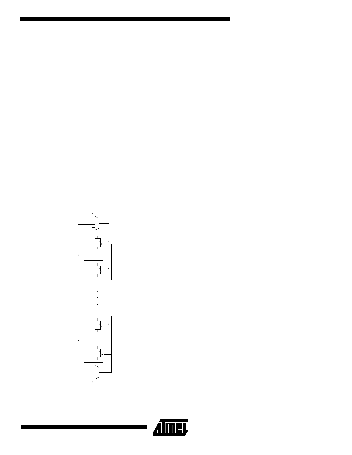
The Symmetrical Array
At the heart of the Atmel architecture is a symmetrical array
of identical cells ( Figure 1). The arr ay is continuous and
completely uninterrupted from one edge to the other,
except for bus repeaters spaced every eight cells
(Figure 2).
In addition to logic and storage, cells can also be used as
wires to connect functions together over shor t distances
and are useful for routing in tight spaces.
The Busing Network
There are two kinds of buses: local and express (see
Figures 2 and 3).
Local buses ar e the link betwe en the array of c ell s and th e
busing network. There are two local buses – North-South 1
and 2 (NS1 and NS2) – for every column of cells, and two
local buses – East-West 1 and 2 (EW1 and EW2) – for
every row of cells. In a sector (an 8 x 8 array of cells
enclosed by repeaters) each local bus is connected to
every cell in its column or row, thus providing every cell in
the array with read/write ac cess to two North-S outh and
two East-West buses.
Figure 1. Symmetrical Array Surrounded by I/O
2
AT6000(LV) Series
Page 3
Figure 2. Busing Network (one sector)
AT6000(LV) Series
CELL
REPEATER
Figure 3. Cell-to-cell and Bus-to-bus Connections
3
Page 4
Each cell, in addition, provides the ability to route a signal
on a 90° turn between the NS1 bus and EW1 bus and
between the NS2 bus and EW2 bus.
Express buses are not con nec ted dir ec tly to cells, and thus
provide higher speeds. They are the fastest way to cover
long, straight-line distances within the array.
Each express bus is paired with a local bus, so there are
two express buses for ever y column and two express
buses for every row of cells.
Connective units, c alled repeaters , spaced every eight
cells, divide each bus, both lo cal and express, into
segments spanning eight cells. Repeaters are aligned in
rows and columns thereby partitioning the array into 8 x 8
sectors of cells. Each repeater is associated with a
local/express pair, and on each side of the repeater are
connections to a local-bus segment and an expr ess-bus
segment. The repeater can be prog rammed to provide any
one of twenty-one connecting functions. These functions
are symmetric with respect to both the two repeater sides
and the two types of buses.
Among the functions provided are the ability to:
• Isolate bus segments from one another
• Connect two local-bus segments
• Connect two express-bus segments
• Implement a local/express transfer
In all of these cases, each connection provides signal
regeneration and is thus u nidirectiona l. For bid irectional
connections, the basic repeater function for the NS2 and
EW2 repeaters is augment ed with a spec ial prog ramm able
connection allowing bidir ectional c ommunicati on between
local-bus segments. This option is primarily used to implement long, tristate buses.
The Cell Structure
The Atmel cell (Figure 4) is simple and small and yet
can be programmed to perform all the logic and wiring
functions needed to implement any digital circuit. Its four
sides are functionall y identical , so each cell is comp letely
symmetrical.
Read/write access to the four local buses – NS1, EW1,
NS2 and EW2 – is controlled, in part, by four bidirectional
pass gates connecte d dir ec tl y to the buse s. T o read a local
bus, the pass gate for that bus is turned on and the threeinput multiplexer is set accordingly. To write to a local bus,
the pass gate for that bus and the pass gate for the associated tristate driver are both turned on. The two-input
multiplexer supplying th e control sig nal to the drivers permits either: (1) active drive, or (2) dy namic tristating
controlled by the B input. Turning between L
between L
NS2
and L
is accomplished by turning on the
EW2
NS1
and L
two associated pass gates. The operations of reading, writing and turning are subject to the restriction that each bus
can be involved in no more than a single operation.
EW1
or
Figure 4. Cell Structure
4
AT6000(LV) Series
Page 5

AT6000(LV) Series
In addition to the four local-bus connections, a cell receives
two inputs and provides two outputs to ea ch of its
North (N), South (S), East (E) and West (W) neighbors.
These inputs and outputs are divided into two classes: “A”
and “B”. There is an A input and a B input from each neighboring cell and an A output and a B output driving all four
neighbors. Between c el ls, an A out put is al way s co nnec te d
to an A input and a B output to a B input.
Within the cell, the four A inputs and the four B inputs enter
two separate, independently configurable multiplexers. Cell
flexibility is enhanced by allowing each multiplexer to select
also the logical constant “1”. The two multiplexer outputs
enter the two upstream AND gates.
Downstream from these two AND gates are an ExclusiveOR (XOR) gate, a register, an AND gate, an inverter and
two four-input multiplexers producing the A and B outputs.
These multiplexers are controlled in tandem (unlike the
A and B input mult iplexe rs) and determi ne the function of
the cell.
• In State 0 – corresponding to the “0” inputs of the
multiplexers – the output of the left-hand upstream AND
gate is connected to the cell’s A output, and the output of
the right-hand upstream AND gate is connected to the
cell’s B output.
• In State 1 – corresponding to the “1” inputs of the
multiplexers – the output of the left-hand upstream AND
gate is connected to the cell’s B output, the output of the
right-hand upstream AND gate is connected to the cell’s
A output.
• In State 2 – corresponding to the “2” inputs of the
multiplexers – the XOR of the outputs from the two
upstream AND gates is provided to the cell’s A output,
while the NAND of these two outputs is provided to the
cell’s B output.
• In State 3 – corresponding to the “3” inputs of the
multiplexers – the XOR function of State 2 is provided to
the D input of a D-type flip-flop, the Q output of which is
connected to the cell’s A output. Clock and
asynchronous reset signals are supplied externally as
described later. The AND of the outputs from the two
upstream AND gates is provided to the cell's B output.
Logic States
The Atmel cell implements a rich and powerful set of logic
functions, stemming from 44 logica l cell states which pe rmutate into 72 physical states. Some states use both A and
B inputs. Other states are created by selecting the “1” input
on either or both of the input multiplexers.
There are 28 combinatoria l primitives created from the
cell’s tristate capabilities and the 20 physical states represented in Figure 5. Five logical primitives are derived from
the physical constants shown in Figure 7. More complex
functions are created by using cells in combination.
A two-input AND feeding an XOR (Figure 8) is produced
using a single cell (F igure 9). A two-to-one multiplexer
selects the logical constant “0” and feeds it to the righthand AND gate. The AND gate acts as a feed- through, l etting the B input pa ss through to the XO R. Th e th r ee-to- on e
multiplexer on the right side selects the local-bus input,
LNS1, and passes it to the left-hand AND gate. The A and
LNS1 signals are the inputs to the AND gat e. Th e outp ut of
the AND gate feeds into the XOR, producing the logic state
l
L) XOR B.
(A
5
Page 6
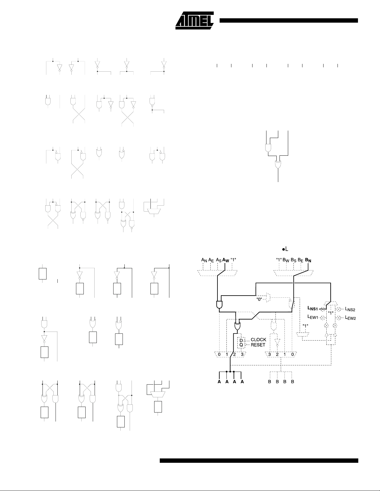
Figure 5. Combinatorial Physical States
A
B
D
Q
"0"
A
B
D
Q
B
D
Q
B
B
D
Q
A
B
D
Q
D
Q
BA
D
Q
A
B
D
Q
B
B
D
Q
BA
B
D
Q
BA
D
Q
B
1
0
L
i
L
i
L
i
L
i
L
i
L
i
L
i
A, L
o
A, L
o
A, L
o
A, L
o
A, L
o
A, L
o
A, L
o
A, L
o
A, L
o
A, L
o
A, L
o
L
i
L
i
L
i
Figure 7. Physical Constants
"0" "0"
"0" "1"
"1" "0"
"1" "1"
A, L
BBABBBB
A, L
o
L
ABBABBABA
i
A, L
o
L
i
A, L
o
L
i
A, L
o
o
L
i
A, L
o
B
B
BA
B
BB A
L
i
A, L
B
o
BA
B
A, L
o
Figure 6. Register States
A, L
A, L
L
A, L
L
A, L
B
A, L
A, L
o
L
i
o
i
o
A, L
A, L
o
L
o
L
i
o
A, L
o
L
i
A
i
A, L
B
o
B
BA
L
i
A, L
B
o
Figure 8. Two-in put AND Feeding XOR
o
B
o
A
i
A, L
BL
B
o
A, L
BA, L
o
A
B
i
B
o
A, L
BA
L
i
B
o
1BA0
A, L
L
i
o
l
Figure 9. Cell Configuration (A
L) XOR B
6
AT6000(LV) Series
Page 7
AT6000(LV) Series
A
D
Q
"1"
GLOBAL
CLOCK
EXPRESS
BUS
GLOBAL
CLOCK
EXPRESS
BUS
R
O
U
T
I
N
G
B
U
R
I
E
D
D
E
D
I
C
A
T
E
D
CELL
D
Q
CELL
A
D
Q
EXPRESS
BUS
GLOBAL
RESET
EXPRESS
BUS
GLOBAL
RESET
CELL
D
Q
CELL
"1"
Clock Distribution
Along the top edge of the array is logic for distributing clock
signals to the D flip-flop in each logic cell (Figure 10). The
distribution network is organiz ed by colum n and permits
columns of cells to be independently clocked. At the head
of each column is a use r- c onf igu ra bl e mul t ip le xe r pr ov id in g
the clock signal for that column. It has four inputs:
• Global clock supplied through the CLOCK pin
• Express bus adjacent to the distribution logic
•“A” output of the cell at the head of the column
• Logical constant “1” to conserve power (no clock)
Through the global clock, the network provides low-skew
distribution of an externa lly supplied clock to any or all of
the columns of the array. The global clock pin is also connected direct ly to the arra y via the A input of the upp er left
and right corner cells (AW on the l eft , an d A N on the r ig ht) .
The express bus is useful in distributing a secondary clock
to multiple colum ns whe n th e glob al cl ock li ne is used a s a
primary clock. The A output of a cell is useful in providing a
clock signal to a single column. T he constan t “1” is used to
reduce power dissipation in columns using no registers.
Figure 10. Column Clock and Column Reset
Asynchronous Reset
Along the bottom edge of the array is logic for asynchronously resetting the D flip-flo ps in the logic cells
(Figure 10). Like the clock network, the asynchronous reset
network is organiz ed by co lu mn a nd p e rmi ts columns to be
independently reset. At the bottom of each column is a
user-configurable multiplexer providing the reset signal for
that column. It has four inputs:
• Global asynchronous reset supplied through the
RESET
• Express bus adjacent to the distribution logic
•“A” output of the cell at the foot of the column
• Logical constant “1” to conserve power
The asynchrono us res et l ogic uses t hese four input s in the
same way that the clock distribution logic does. Through
the global asynchr onous re set, any or all columns can b e
reset by an externally supplied signal. The global asynchronous reset pin is also connected directly to the array via the
A input of the lower left and right corner cells (AS on the
left, and AE on the ri ght). T he expr ess bu s can be used t o
distribute a secondary reset to multiple columns when the
global reset line is used as a prim ary reset, the A outp ut of
a cell can also pro vide an asyn chrono us reset signal to a
single column, and the constant “1” is used by columns
with registers requi ring no re se t. A ll regis te rs are re se t du ring power-up.
pin
Input/Output
The Atmel architecture provides a flexible interface
between the logic arra y, the confi gurati on contro l logic an d
the I/O pins.
Two adjacent cells – an “exit” and an “entranc e” cell – on
the perimeter of the logic array are associated with each
I/O pin.
There are two type s of I/Os: A-type (F igure 11) and B-typ e
(Figure 12). For A-type I/Os, the edge-facing A output of an
exit cell is connected to an output driver, and the edgefacing A input of the adjacent entr ance cell is connecte d to
an input buffer. The output of the output driver and the input
of the input buffer are connected to a common pin.
B-type I/Os are the same as A-type I/Os, but use the B
inputs and outputs of their respective entrance and exit
cells. A- and B-type I/Os altern ate arou nd the array Control
of the I/O logic is provided by user-configurable memory
bits.
7
Page 8
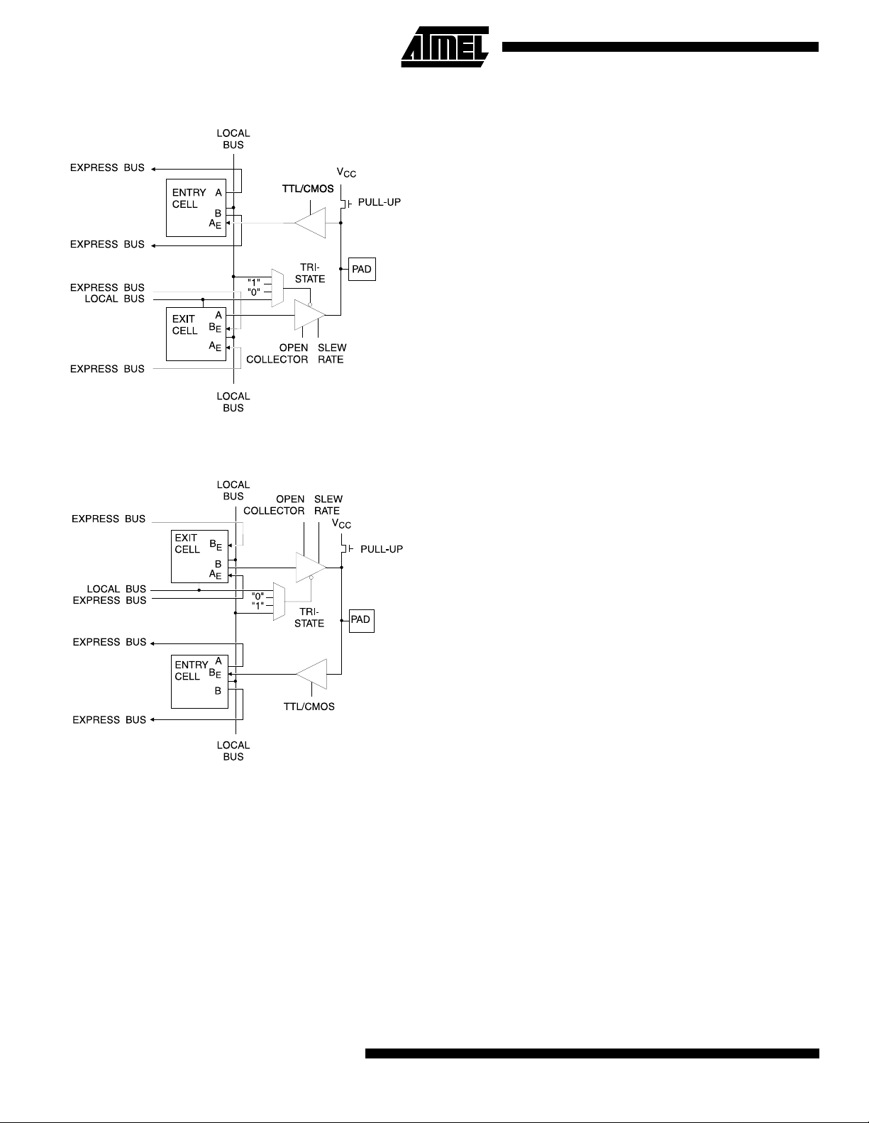
Figure 11. A-type I/O Logic
Figure 12. B-type I/O Logic
Slew Rate Control
A user-configurabl e bit co ntrols th e slew rate – fast or slow
– of the output buffer. A s low slew rate, which reduces
noise and ground bounce, is recommended for outputs that
are not speed-critical. Fast and slow slew rates have the
same DC-current sinking capabilities, but the rate at which
each allows the output devices to reach full drive differs.
Pull-up
A user-configurab le bit cont rols the pull -up tran sistor in the
I/O pin. It’s primary function is to pro vide a logica l “1” to
unused input pi ns. When on , it is appro ximat ely equi valen t
to a 25K resistor to V
Enable Select
User-configurable bits determine the output-enable for the
output driver. The output driver can be static – always on or
always off – or dynamically controlled by a signal generated in the array. Four options are ava il able fr om the array :
(1) the control is low and always driv ing; (2) the control is
high and never driving; (3) the control is connected to a vertical local bus associated with the output cell; or (4) the
control is connected to a horizontal local bus assoc iated
with the output cell. On power- up, the us er I/Os ar e configured as inputs with pull-up resistors.
In addition to the fu nction al ity p ro vided b y the I/O l ogi c , th e
entrance and exit cells provide the ability to register both
inputs and outputs . Also , th ese per imeter c ells (unli ke in terior cells) are conne cted directly to expres s buses: the
edge-facing A and B outputs of the entrance cell are c onnected to express buses, as are the edge-facing A and B
inputs of the exit cell. These buses are perpendicular to the
edge, and provide a rapid means of bringing I/O signals to
and from the array interi or and the opposite ed ge of the
chip.
CC
.
TTL/CMOS Inputs
A user-configurable bit determines the threshold level –
TTL or CMOS – of the input buffer.
Open Collector/Tristate Outputs
A user-configurable bit which enables or disables the active
pull-up of the output device.
8
AT6000(LV) Series
Chip Configuration
The Integrated Development System generates the SRAM
bit pattern required to con f ig ure a AT 60 00 S erie s d ev ice. A
PC parallel port, microprocessor, EPROM or serial configuration memory can be used to download configuration
patterns.
Users select from several configuration modes. Many factors, including board area, configuration speed and the
number of designs implemented in parallel can influence
the user’s final choice.
Configuration is controlled by dedicated configuration pins
and dual-function pins that double as I/O pins when the
device is in op eration. T he number of dual-funct ion pins
required for each mode varies.
Page 9

AT6000(LV) Series
The devices can be partially reconfigured while in operation. Portions of the device not being modified remain
operational during recon figuratio n. Simul taneous configuration of more th an one device is al so possible. Full
configuration takes as little as a millisecond, partial configuration is even faster.
Refer to the Pin Function Description section following for a
brief summary of the pins used in configur ation. For more
information about c onfi gurat ion, refer to the AT6 000 Series
Configuration data sheet.
Pin Function Description
This section provides abbreviated descriptions of the various AT6000 Series pins. For more complete descriptions,
refer to the AT6000 Series Configuration data sheet.
Pinout tables for the AT6000 series of devices follow.
Power Pins
VCC, VDD, GND, V
VCC and GND are the I/O supply pins, VDD and VSS are the
internal logic supply pins. V
same trace on the printed circuit board. GND and V
should be tied to the same trace on the printed circuit
board.
Input/Output Pins
All I/O pins can be used in the same way ( refer to the I/O
section of the architecture description). Some I/O pins are
dual-function pins used during configuration of the array.
When not being used for configu ration, dua l-functio n I/Os
are fully functional as normal I/O pins. On initial power-up,
all I/Os are configured as TTL inputs with a pull-up.
Dedicated Timing and Control Pins
CON
Configuration-in-process pin. After power-up, CO N staysLow until power-up init ial ization is complete, at which tim e
is then released. CON is an open collecto r signal .
CON
After power-up initialization, forcing CON
configuration process.
CS
Configuration enable p in. Al l conf igura tion pi ns are i gnore d
is high. CS must be held low thro ughout the conf igu-
if CS
ration pr ocess. CS
SS
and VDD should be tied to the
CC
is a TTL input pin.
SS
low begins the
M0, M1, M2
Configuration mo de pins are used to d etermine the confi guration mode. All three are TTL input pins.
CCLK
Configuration clock pin. CCLK is a TTL input or a CMOS
output depending on the mod e of o per at ion . In m ode s 1, 2,
3, and 6 it is an input. In modes 4 and 5 it i s an outp ut with
a typical frequency of 1 MHz. In all modes, the rising edge
of the CCLK signal is used to sample inputs and change
outputs.
CLOCK
External logic s ourc e us ed to d rive the in ter nal gl oba l c lock
line. Registers toggle on the risi ng edge of CLOCK. T he
CLOCK signal is neither used nor affected by the configuration modes. It is always a TTL input.
RESET
Array register async hrono us reset. RESET drives the internal global reset. The RESET
affected by the configuration modes. It is always a TTL
input.
Dual-function Pins
When CON
I/Os; when CON
figuration c ontrol or data si gnals as deter mined by the
configuration modes. Care must be taken wh en using
these pins to ens ure that conf iguration ac tivity does no t
interfere with other circuitry connected to these pins in the
application.
D0 or I/O
Serial configuration modes use D0 as the serial data input
pin. Parallel configuratio n modes us e D0 as the least-significant bit. Input d ata must meet setup and hold
requirements with respect to the rising edge of CCLK. D0 is
a TTL input during configuration.
D1 to D7 or I/O
Parallel conf iguration mo des use these pi ns as inputs.
Serial configuration modes do not use them. Data must
meet setup and hold requirements with respect to the rising
edge of CCLK. D1 - D7 are TTL inputs during configuration.
A0 to A16 or I/O
During configuration in modes 1, 2 and 5, these pins are
CMOS outputs and act as the address pins for a parallel
EPROM. A0 - A16 eliminates the need for an external
address counter when using an external parallel nonvolatile
is high, dual -functio n I/O pins ac t as devic e
is low, dual-function pins are used as con-
signal is neither used nor
9
Page 10

memory to configure the FPGA. Addresses change after
the rising edge of the CCLK signal.
CSOUT
When cascading devices, CSOUT is an output used to
enable other devices. CSOUT
CS
optional and ca n be disabled du ring initial programmin g
when cascading is not u sed. When cascadin g devices,
CSOUT
as a configurable I/O.
CHECK
During configuration, CHECK is a TTL input that can be
used to enable the data check function at the beginning of
a configuration cycle . No data i s written t o the devic e whil e
CHECK
to D0 (or D0 - D7, in paralle l mode) is comp ared with the
or I/O
should be connected to the
input of the downstream device. The CSOUT function is
should be dedi cated to co nfigurati on an d n ot used
or I/O
is low. Instead , t he conf igu ration file bei ng ap plie d
current contents of the internal configuration RAM. If a mismatch is detected between the data being loaded and the
data already in the RAM, the ERR
CHECK
tial programming.
ERR
During configuration, ERR is an output. When the CHECK
function is activated and a mismatch is detected between
the current co nfigu ratio n data st ream and the data alrea dy
loaded in the conf igurat ion RAM, ER R
ouput is a registered s ig nal . On ce a m is mat ch is foun d, th e
signal is set and is only reset after the configuration cycle is
restarted. ERR
The ERR
initial programming.
function is optional and c an be dis abled duri ng ini-
or I/O
is also asserted fo r co nfi gurati on fil e e rror s .
function is optional and can be disabled during
pin goes low. The
goes low. Th e E RR
Device Pinout Selection (Max. Number of User I/O)
AT6002 AT6003 AT6005 AT6010
84 PLCC 64 I/O 64 I/O 64 I/O 100 VQFP 80 I/O 80 I/O 80 I/O 132 PQFP 96 I/O 108 I/O 108 I/O 108 I/O
144 TQFP 95 I/O 120 I/O 108 I/O 120 I/O
208 PQFP - - - 172 I/O
240 PQFP - - - 204 I/O
Bit-stream Sizes
Mode(s) Typ e Beginning Sequence AT6002 AT6003 AT6005 AT6010
1 Parallel Preamble 2677 4153 8077 16393
2 Parallel Preamble 2677 4153 8077 16393
3 Serial Null Byte/Preamble 2678 4154 8078 16394
4 Serial Null Byte/Preamble 2678 4154 8078 16394
5 Parallel Preamble 2677 4153 8077 16393
6 Parallel Preamble/Preamble 2678 4154 8078 16394
10
AT6000(LV) Series
Page 11

AT6000(LV) Series
Pinout Assignment
Left Side (Top to Bottom)
84
AT6002 AT6003 AT6005 AT6010
---I/O51(A)----B111
I/O24(A) or A7 I/O30(A) or A7 I/O27(A) or A7 I/O50(A) or A7 12 1 18 1 C1 2 2
- I/O29(B) - I/O49(A) - - -2D133
---I/O48(B)------4
---VCC----PWR
---I/O47(A)----E156
---GND----GND
- I/O28(A) I/O26(A) I/O46(A) - - 19 3 G1 7 8
I/O23(A) or A6 I/O27(A) or A6 I/O25(A) or A6 I/O45(A) or A6 13 2 20 4 H1 8 9
- - - I/O44(B) - - - - - - 10
- - - I/O43(A) - - - - C2 9 11
I/O22(B) I/O26(A) I/O24(A) I/O42(A) - - 21 5 D2 10 12
I/O21(A) or A5 I/O25(A) or A5 I/O23(A) or A5 I/O41(A) or A5 14 3 22 6 E2 11 13
- - - I/O40(B) - - - - - - 14
---I/O39(A)----F21215
I/O20(B) I/O24(B) I/O22(A) I/O38(A) - 4 23 7 G2 13 16
I/O19(A) or A4 I/O23(A) or A4 I/O21(A) or A4 I/O37(A) or A4 15 5 24 8 H2 14 17
- - - I/O36(B) - - - - - - 18
I/O18(B) I/O22(B) I/O20(A) I/O35(A) - - 25 9 D3 15 19
I/O17(A) or A3 I/O21(A) or A3 I/O19(A) or A3 I/O34(A) or A3 16 6 26 10 E3 16 20
I/O16(B) I/O20(B) I/O18(A) I/O33(A) - 7 27 11 F3 17 21
- - - I/O32(B) - - - - - 18 22
I/O15(A) or A2 I/O19(A) or A2 I/O17(A) or A2 I/O31(A) or A2 17 8 28 12 G3 19 23
- I/O18(B) I/O16(A) I/O30(A) - - 29 13 H3 20 24
GND GND GND GND 18 9 30 14 GND
VSS VSS VSS VSS 19 10 31 15 GND
I/O14(A) or A1 I/O17(A) or A1 I/O15(A) or A1 I/O29(A) or A1 20 11 32 16 F4 23 27
- - - I/O28(B) - - - - - 24 28
- I/O16(B) - I/O27(A) - - - 17 G4 25 29
I/O13(A) or A0 I/O15(A) or A0 I/O14(A) or A0 I/O26(A) or A0 21 12 33 18 H4 26 30
I/O12(B) or D7 I/O14(A) or D7 I/O13(A) or D7 I/O25(B) or D7 22 13 34 19 H5 27 31
- - - I/O24(B) - - - - - 28 32
I/O11(A) or D6 I/O13(A) or D6 I/O12(A) or D6 I/O23(A) or D6 23 14 35 20 J4 29 33
I/O10(A) or D5 I/O12(A) or D5 I/O11(A) or D5 I/O22(A) or D5 24 15 36 21 K4 30 34
VDD VDD VDD VDD 25 16 37 22 PWR
VCC VCC VCC VCC 26 17 38 23 PWR
PLCC
100
VQFP
132
PQFP
144
TQFP
180
CPGA
(1)
(2)
(2)
(2)
(1)
(1)
208
PQFP
45
67
21 25
22 26
31 35
32 36
240
PQFP
11
Page 12

Pinout Assignment (Continued)
Left Side (Top to Bottom)
AT6002 AT6003 AT6005 AT6010
I/O9(B) I/O11(B) I/O10(A) I/O21(A) - - 39 24 J3 33 37
- - - I/O20(B) - - - - - 34 38
I/O8(A) or D4 I/O10(A) or D4 I/O9(A) or D4 I/O19(A) or D4 27 18 40 25 K3 35 39
I/O7(B) I/O9(B) I/O8(A) I/O18(A) - 19 41 26 L3 36 40
---I/O17(A)----M33741
- - - I/O16(B) - - - - - - 42
I/O6(A) or D3 I/O8(A) or D3 I/O7(A) or D3 I/O15(A) or D3 28 20 42 27 N3 38 43
- I/O7(B) I/O6(A) I/O14(A) - - 43 28 J2 39 44
---I/O13(A)----K24045
GND GND GND GND - - 44 29 GND
---VSS----GND
- - - I/O12(B) - - - - - - 48
I/O5(A) or D2 I/O6(A) or D2 I/O5(A) or D2 I/O11(A) or D2 29 21 45 30 M2 43 49
I/O4(B) I/O5(B) I/O4(A) I/O10(A) - 22 46 31 N2 44 50
---I/O9(A)----P24551
---I/O8(B)------52
I/O3(A) or D1 I/O4(A) or D1 I/O3(A) or D1 I/O7(A) or D1 30 23 47 32 J1 46 53
I/O2(B) I/O3(A) I/O2(A) I/O6(A) - - 48 33 K1 47 54
---I/O5(A)----L14855
---I/O4(B)------56
- I/O2(B) - I/O3(A) - - - 34 M1 49 57
I/O1(A) or D0 I/O1(A) or D0 I/O1(A) or D0 I/O2(A) or D0 31 24 49 35 N1 50 58
---I/O1(A)----P15159
CCLK CCLK CCLK CCLK 32 25 50 36 R1 52 60
84
PLCC
Notes: 1. PWR = Pins connected to power plane = F1, E4/E5, L2, R4, K15, L12, E14, A12.
2. GND = Pins connected to ground plane = L4, M4, N9, N10, E12, D12, C7, C6.
100
VQFP
132
PQFP
144
TQFP
180
CPGA
(2)
(2)
208
PQFP
41 46
42 47
240
PQFP
12
AT6000(LV) Series
Page 13

AT6000(LV) Series
Pinout Assignment
Bottom Side (Left to Right)
84
AT6002 AT6003 AT6005 AT6010
CON
- - - I/O204(A) - - - - M6 54 62
I/O96(A) I/O120(A) I/O108(A) I/O203(A) 34 27 52 38 M7 55 63
- I/O119(B) - I/O202(A) - - - 39 R2 56 64
- - - I/O201(B) - - - - - - 65
- - - VCC ----PWR
- - - I/O200(A) - - - - R3 58 67
- - - GND ----GND
- I/O118(A) I/O107(A) I/O199(A) - - 53 40 R5 60 69
I/O95(A) or
CSOUT
- - - I/O197(B) - - - - - - 71
- - - I/O196(A) - - - - R7 62 72
I/O94(B) I/O116(A) I/O105(A) I/O195(A) - - 55 42 P3 63 73
I/O93(A) I/O115(A) I/O104(A) I/O194(A) 36 29 56 43 P4 64 74
- - - I/O193(B) - - - - - - 75
- - - I/O192(A) - - - - P5 65 76
I/O92(B) I/O114(B) I/O103(A) I/O191(A) - 30 57 44 P6 66 77
I/O91(A) or
CHECK
- - - I/O189(B) - - - - - - 79
I/O90(B) I/O112(B) I/O101(A) I/O188(A) - - 59 46 N4 68 80
I/O89(A) or
ERR
I/O88(B) I/O110(B) I/O99(A) I/O186(A) - 33 61 48 N6 70 82
- - - I/O185(B) - - - - - 71 83
I/O87(A) I/O109(A) I/O98(A) I/O184(A) 39 34 62 49 N7 72 84
- I/O108(B) I/O97(A) I/O183(A) - - 63 50 M8 73 85
GND GND GND G ND 40 35 64 51 GND
I/O86(A) I/O107(A) I/O96(A) I/O182(A) 41 36 65 52 M9 75 87
- - - I/O181(B) - - - - - 76 88
- I/O106(B) - I/O180(A) - - - 53 M10 77 89
I/O85(A) I/O105(A) I/O95(A) I/O179(A) 42 37 66 54 M11 78 90
CS
I/O84(B) I/O104(A) I/O94(A) I/O178(A) 44 39 68 56 M12 80 92
- - - I/O177(B) - - - - - 81 93
I/O83(A) I/O103(A) I/O93(A) I/O176(A) 45 40 69 57 N8 82 94
CON CON CON 33 26 51 37 M5 53 61
I/O117(A) or
CSOUT
I/O113(A) or
CHECK
I/O111(A) or
ERR
CS CS CS 43 38 67 55 L8 79 91
I/O106(A) or
CSOUT
I/O102(A) or
CHECK
I/O100(A) or
ERR
I/O198(A) or
CSOUT
I/O190(A) or
CHECK
I/O187(A) or
ERR
PLCC
35 28 54 41 R6 61 70
37 31 58 45 P7 67 78
38 32 60 47 N5 69 81
100
VQFP
132
PQFP
144
TQFP
180
CPGA
(1)
(2)
(2)
208
PQFP
57 66
59 68
74 86
240
PQFP
13
Page 14

Pinout Assignment (Continued)
Bottom Side (Left to Right)
AT6002 AT6003 AT6005 AT6010
- - - VDD ----PWR
VCC VCC VCC VCC 46 41 70 58 PWR
I/O82(A) I/O102(A) I/O92(A) I/O175(A) 47 42 71 59 N11 85 97
I/O81(B) I/O101(B) I/O91(A) I/O174(A) - - 72 60 N12 86 98
- - - I/O173(B) - - - - - 87 99
I/O80(A) I/O100(A) I/O90(A) I/O172(A) 48 43 73 61 N13 88 100
I/O79(B) I/O99(B) I/O89(A) I/O171(A) - 44 74 62 P8 89 101
- - - I/O170(A) - - - - P9 90 102
- - - I/O169(B) - - - - - - 103
I/O78(A) I/O98(A) I/O88(A) I/O168(A) 49 45 75 63 P10 91 104
- I/O97(B) I/O87(A) I/O167(A) - - 76 64 P11 92 105
- - - I/O166(A) - - - - P12 93 106
GND GND GND GND - - 77 65 GND
- - - I/O165(B) - - - - - - 108
I/O77(A) I/O96(A) I/O86(A) I/O164(A) 50 46 78 66 P13 95 109
I/O76(B) I/O95(B) I/O85(A) I/O163(A) - 47 79 67 P14 96 110
- - - I/O162(A) - - - - P8 97 111
- - - I/O161(B) - - - - - - 112
I/O75(A) I/O94(A) I/O84(A) I/O160(A) 51 48 80 68 R9 98 113
I/O74(B) I/O93(A) I/O83(A) I/O159(A) - - 81 69 R10 99 114
- - - I/O158(A) - - - - R11 100 115
- - - I/O157(B) - - - - - - 116
- I/O92(B) - I/O156(A) - - - 70 R12 101 117
I/O73(A) I/O91(A) I/O82(A) I/O155(A) 52 49 82 71 R13 102 118
- - - I/O154(A) - - - - R14 103 119
RESET
RESET RESET RESET 53 50 83 72 R15 104 120
84
PLCC
Notes: 1. PWR = Pins connected to power plane = F1, E4/E5, L2, R4, K15, L12, E14, A12.
2. GND = Pins connected to ground plane = L4, M4, N9, N10, E12, D12, C7, C6.
100
VQFP
132
PQFP
144
TQFP
180
CPGA
(1)
(1)
(2)
208
PQFP
83 95
84 96
94 107
240
PQFP
14
AT6000(LV) Series
Page 15

AT6000(LV) Series
Pinout Assignment
Right Side (Bottom to Top)
84
AT6002 AT6003 AT6005 AT6010
PLCC
- - - I/O153(A) - - - - P15 105 121
I/O72(A) I/O90(A) I/O81(A) I/O152(A) 54 51 84 73 N15 106 122
- I/O89(B) I/O80(A) I/O151(A) - - 85
- - - I/O150(B) - - - - - - 124
- - - VCC ----PWR
- - - I/O149(A) - - - - L15 109 126
- - - GND ----GND
- I/O88(A) - I/O148(A) - - 85
I/O71(A) I/O87(A) I/O79(A) I/O147(A) 55 52 86 76 H15 112 129
- - - I/O146(B) - - - - - - 130
- - - I/O145(A) - - - - N14 113 131
I/O70(B) I/O86(A) I/O78(A) I/O144(A) - - 87 77 M14 114 132
I/O69(A) I/O85(A) I/O77(A) I/O143(A) 56 53 88 78 L14 115 133
- - - I/O142(B) - - - - - - 134
- - - I/O141(A) - - - - K14 116 135
I/O68(B) I/O84(B) I/O76(A) I/O140(A) - 54 89 79 J14 117 136
I/O67(A) I/O83(A) I/O75(A) I/O139(A) 57 55 90 80 H14 118 137
- - - I/O138B - - - - - - 138
I/O66(B) I/O82(B) I/O74(A) I/O137(A) - - 91 81 M13 119 139
I/O65(A) I/O81(A) I/O73(A) I/O136(A) 58 56 92 82 L13 120 140
I/O64(B) I/O80(B) I/O72(A) I/O135(A) - 57 93 83 K13 121 141
- - - I/O134(B) - - - - - 122 142
I/O63(A) I/O79(A) I/O71(A I/O133(A) 59 58 94 84 J13 123 143
- I/O78(B) I/O70(A) I/O132(A) - - 95 85 H13 124 144
GND GND GND G ND 60 59 96 86 GND
VSS VSS VSS VSS 61 60 97 87 GND
I/O62(A) I/O77(A) I/O69(A) I/O131(A) 62 61 98 88 K12 127 147
- - - I/O130(B) - - - - - 128 148
- I/O76(B) - I/O129(A) - - - 89 J12 129 149
I/O61(A) I/O75(A) I/O68(A) I/O128(A) 63 62 99 90 H12 130 150
I/O60(B) I/O74(A) I/O67(A) I/O127(A) 64 63 100 91 H11 131 151
- - - I/O126(B) - - - - - 132 152
I/O59(A) I/O73(A) I/O66(A) I/O125(A) 65 64 101 92 G12 133 153
I/O58(A) I/O72(A) I/O65(A) I/O124(A) 66 65 102 93 F12 134 154
VDD VDD VDD VDD 67 66 103 94 PW R
VCC VCC VCC VCC 68 67 104 95 PW R
100
VQFP
132
PQFP
(3)
(4)
144
TQFP
180
CPGA
208
PQFP
74 M15 107 123
(1)
108 125
(2)
110 127
75 J15 111 128
(2)
125 145
(2)
126 146
(1)
135 155
(1)
136 156
240
PQFP
15
Page 16

Pinout Assignment (Continued)
Right Side (Bottom to Top)
AT6002 AT6003 AT6005 AT6010
I/O57(B) I/O71(B) I/O64(A) I/O123(A) - - 105 96 G13 137 157
- - - I/O122(B) - - - - - 138 158
I/O56(A) I/O70(A) I/O63(A) I/O121(A) 69 68 106 97 F13 139 159
I/O55(B) I/O69(B) I/O62(A) I/O120(A) - 69 107 98 E13 140 160
- - - I/O119(A) - - - - D13 141 161
- - - I/O118(B) - - - - - - 162
I/O54(A) I/O68(A) I/O61(A) I/O117(A) 70 70 108 99 C13 142 163
- I/O67(B) I/O60(A) I/O116(A) - - 109 100 G14 143 164
- - - I/O115(A) - - - - F14 144 165
GND GND GND GND - - 110 101 GND
- - - VSS ----GND
- - - I/O114(B) - - - - - - 168
I/O53(A) I/O66(A) I/O59(A) I/O113(A) 71 71 111 102 D14 147 169
I/O52(B) I/O65(B) I/O58(A) I/O112(A) - 72 112 103 C14 148 170
- - - I/O111(A) - - - - B14 149 171
- - - I/O110(B) - - - - - - 172
I/O51(A) I/O64(A) I/O57(A) I/O109(A) 72 73 113 104 G15 150 173
I/O50(B) I/O63(A) I/O56(A) I/O108(A) - - 114 105 F15 151 174
- - - I/O107(A) - - - - E15 152 175
- - - I/O106(B) - - - - - - 176
- I/O62(B) - I/O105(A) - - - 106 D15 153 177
I/O49(A) I/O61(A) I/O55(A) I/O104(A) 73 74 115 107 C15 154 178‘
- - - I/O103(A) - - - - B15 155 179
M2 M2 M2 M2 74 75 116 108 A15 156 180
84
PLCC
Notes: 1. PWR = Pins connected to power plane = F1, E4/E5, L2, R4, K15, L12, E14, A12.
2. GND = Pins connected to ground plane = L4, M4, N9, N10, E12, D12, C7, C6.
3. 85 = Pin 85 on AT6005.
4. 85 = Pin 85 on AT6003 and AT6010.
100
VQFP
132
PQFP
144
TQFP
180
CPGA
(2)
(2)
208
PQFP
145 166
146 167
240
PQFP
16
AT6000(LV) Series
Page 17

AT6000(LV) Series
Pinout Assignment
Top Side (Right to Left)
84
AT6002 AT6003 AT6005 AT6010
M1 M1 M1 M1 75 76 117 109 D11 157 181
- - - I/O102(A) - - - - D10 158 182
I/O48(A) I/O60(A) I/O54(A) I/O101(A) 76 77 118 110 D9 159 183
- I/O59(B) - I/O100(A) - - - 111 A14 160 184
- - - I/O99(B) - - - - - - 185
- - - VCC ----PWR
- - - I/O98(A) - - - - A13 162 187
- - - GND ----GND
- I/O58(A) I/O53(A) I/O97(A) - - 119 112 A11 164 189
I/O47(A) I/O57(A) I/O52(A) I/O96(A) 77 78 120 113 A10 165 190
- - - I/O95(B) - - - - - - 191
- - - I/O94(A) - - - - A 9 166 192
I/O46(B) I/O56(A) I/O51(A) I/O93(A) - - 121 114 B13 167 193
I/O45(A) I/O55(A) I/O50(A) I/O92(A) 78 79 122 115 B12 168 194
- - - I/O91(B) - - - - - - 195
- - - I/O90(A) - - - - B11 169 196
I/O44(B) I/O54(B) I/O49(A) I/O89(A) - 80 123 116 B10 170 197
I/O43(A) I/O53(A) I/O48(A) I/O88(A) 79 81 124 117 B9 171 198
- - - I/O87(B) - - - - - - 199
I/O42(B) I/O52(B) I/O47(A) I/O86(A) - - 125 118 C12 172 200
I/O41(A) I/O51(A) I/O46(A) I/O85(A) 80 82 126 119 C11 173 201
I/O40(B) I/O50(B) I/O45(A) I/O84(A) - 83 127 120 C10 174 202
- - - I/O83(B) - - - - - 175 203
I/O39(A) I/O49(A) I/O44(A) I/O82(A) 81 84 128 121 C9 176 204
- I/O48(B) I/O43(A) I/O81(A) - - 129 122 D8 177 205
GND GND GND G ND 82 85 130 123 GND
I/O38(A) I/O47(A) I/O42(A) I/O80(A) 83 86 131 124 D7 179 207
- - - I/O79(B) - - - - - 180 208
- I/O46(B) - I/O78(A) - - - 125 D6 181 209
I/O37(A) or A16 I/O45(A) or A16 I/O41(A) or A16 I/O77(A) or A16 84 87 132 126 D5 182 210
CLOCK CLOCK CLOCK CLOCK 1 88 1 127 E8 183 211
I/O36(B) or A15 I/O44(B) or A15 I/O40(A) or A15 I/O76(A) or A15 2 89 2 128 D4 184 212
- - - I/O75(B) - - - - - 185 213
I/O35(A) or A14 I/O43(A) or A14 I/O39(A) or A14 I/O74(A) or A14 3 90 3 129 C8 186 214
- - - VDD ----PWR
VCC VCC VCC VCC 4 91 4 130 PWR
PLCC
100
VQFP
132
PQFP
144
TQFP
180
CPGA
(1)
(2)
(2)
(1)
(1)
208
PQFP
161 186
163 188
178 206
187 215
188 216
240
PQFP
17
Page 18

Pinout Assignment (Continued)
Top Side (Right to Left)
AT6002 AT6003 AT6005 AT6010
I/O34(A) or A13 I/O42(A) or A13 I/O38(A) or A13 I/O73(A) or A13 5 92 5 131 C5 189 217
I/O33(B) I/O41(B) I/O37(A) I/O72(A) - - 6 132 C4 190 218
- - - I/O71(B) - - - - - 191 219
I/O32(A) or A12 I/O40(A) or A12 I/O36(A) or A12 I/O70(A) or A12 6 93 7 133 C3 192 220
I/O31(B) I/O39(B) I/O35(A) I/O69(A) - 94 8 134 B8 193 221
- - - I/O68(A) - - - - B 7 194 222
- - - I/O67(B) - - - - - - 223
I/O30(A) or A11 I/O38(A) or A11 I/O34(A) or A11 I/O66(A) or A11 7 95 9 135 B6 195 224
- I/O37(B) I/O33(A) I/O65(A) - - 10 136 B5 196 225
- - - I/O64(A) - - - - B 4 197 226
GND GND GND GND - - 11 13 7 GND
- - - I/O63(B) - - - - - - 228
I/O29(A) or A10 I/O36(A) or A10 I/O32(A) or A10 I/O62(A) or A10 8 96 12 138 B3 199 229
I/O28(B) I/O35(B) I/O31(A) I/O61(A) - 97 13 13 9 B2 200 230
- - - I/O60(A) - - - - A 8 201 231
- - - I/O59(B) - - - - - - 232
I/O27(A) or A9 I/O34(A) or A9 I/O30(A) or A9 I/O58(A) or A9 9 98 14 140 A7 202 233
I/O26(B) I/O33(A) I/O29(A) I/O57(A) - - 15 141 A 6 203 234
- - - I/O56(A) - - - - A 5 204 235
- - - I/O55(B) - - - - - - 236
- I/O32(B) - I/O54(A) - - - 142 A4 205 237
I/O25(A) or A8 I/O31(A) or A8 I/O28(A) or A8 I/O53(A) or A8 10 99 16 143 A3 206 238
- - - I/O52(A) - - - - A2 -207 239
M0 M0 M0 M0 11 100 17 144 A1 208 240
84
PLCC
Notes: 1. PWR = Pins connected to power plane = F1, E4/E5, L2, R4, K15, L12, E14, A12.
2. GND = Pins connected to ground plane = L4, M4, N9, N10, E12, D12, C7, C6.
100
VQFP
132
PQFP
144
TQFP
180
CPGA
(2)
208
PQFP
198 227
240
PQFP
18
AT6000(LV) Series
Page 19

AT6000(LV) Series
AC Timing Characteristics – 5V Operation
Delays are based on fixed lo ad. Loads for eac h type of device ar e described in the no tes. Delays are in nanosecon ds.
Worst case: V
Cell Function Parameter From To
(4)
Wire
= 4.75V to 5.25V. Temperature = 0°C to 70°C.
CC
tPD (max)
(4)
A, B, L A, B 1 0.8 1.2 1.8 ns
Load
Definition
(7)
-1 -2 -4 Units
NAND t
XOR t
AND t
(max) A, B, L B 1 1.6 2.2 3.2 ns
PD
(max) A, B, L A 1 1.8 2.4 4.0 ns
PD
(max) A, B, L B 1 1.7 2.2 3.2 ns
PD
A, B A 1
1.7 2.3 4.0 ns
MUX tPD (max)
D-Flip-flop
D-Flip-flop
(5)
(5)
D-Flip-flop t
LA1
t
(min) A, B, L CLK - 1.5 2.0 3.0 ns
setup
t
(min) CLK A, B, L - 000ns
hold
(max) CLK A 1 1.5 2.0 3.0 ns
PD
2.1 3.0 4.9 ns
Bus Driver tPD (max) A L 2 2.0 2.6 4.0 ns
L, E E 3
1.3 1.6 2.3 ns
Repeater tPD (max)
L, E L 2
1.7 2.1 3.0 ns
Column Clock tPD (max) GCLK, A, ES CLK 3 1.8 2.4 3.0 ns
Column Reset t
Clock Buffer
Reset Buffer
TTL Input
CMOS Input
Fast Output
Slow Output
Output Disable
Fast Enable
Slow Enable
(5)
(5)
(1)
(2)
(3)
(3)
(5)
(3)(5)
(3)(5)
(max) GRES, A, EN RES 3 1.8 2.4 3.0 ns
PD
tPD (max) CLOCK PIN GCLK - 1.6 2.0 2.9 ns
tPD (max) RESET PIN GRES - 1.5 1.9 2.8 ns
tPD (max) I/O A 3 1.0 1.2 1.5 ns
tPD (max) I/O A 3 1.3 1.4 2.3 ns
tPD (max) A I/O PIN 4 3.3 3.5 6.0 ns
tPD (max) A I/O PIN 4 7.5 8.0 12.0 ns
t
(max) L I/O PIN 4 3.1 3.3 5.5 ns
PXZ
t
(max) L I/O PIN 4 3.8 4.0 6.5 ns
PXZ
t
(max) L I/O PIN 4 8.2 8.5 12.5 ns
PXZ
Device Cell Types Outputs I
(6)
Cell
(6)
Bus
Column Clock
(6)
Wire, XWire, Half-adder, Flip-flop A, B 4.5 µA/MHz
Wire, XWire, Half-adder, Flip-flop, Repeater L 2.5 µA/MHz
Column Clock Driver CLK 40 µA/MHz
(max)
CC
Notes: 1. TTL buffer delays are measured from a VIH of 1.5V at the pad to the internal VIH at A. The input buffer load is constant.
2. CM OS b uff er del a ys are measure d from a V
of 1/2 VCC at the apd to the internal VIH at A. The input buffer load is con sta nt.
IH
3. Buffer delay is to a pad voltage of 1.5V with one output switching.
4. Max specifications are the average of mas t
PDLH
and t
PDHL
.
5. Parameter based on characterization and simulation; not tested in production
6. Exact power calculation is available in an Atmel application note.
7. Load Definition: 1 = Load of one A or B input; 2 = Load of one L input; 3 = Constant Load; 4 = Tester Load of 50 pF.
= Preliminary Information
19
Page 20

AC Timing Characteristics – 3.3V Operation
Delays are based on fixed lo ad. Loads for eac h type of device ar e described in the no tes. Delays are in nanosecon ds.
Worst case: V
Cell Function Parameter From To
(4)
Wire
= 3.0V to 3.6V. Temperature = 0°C to 70°C.
CC
tPD (max)
(4)
Load
Definition
(7)
-4 Units
A, B, L A, B 1 1.8 ns
NAND t
(max) A, B, L B 1 3.2 ns
PD
XOR tPD (max) A, B, L A 1 4.0 ns
AND t
(max) A, B, L B 1 3.2 ns
PD
A, B A 1 4.0 ns
MUX t
D-Flip-flop
D-Flip-flop
(5)
(5)
(max)
PD
t
(min) A, B, L CLK - 3.0 ns
setup
t
(min) CLK A, B, L - 0 ns
hold
LA14.9ns
D-Flip-flop tPD (max) CLK A 1 3.0 ns
Bus Driver t
(max) A L 2 4.0 ns
PD
L, E E 3 2.3 ns
Repeater t
PD
(max)
L, E L 2 3.0 ns
Column Clock tPD (max) GCLK, A, ES CLK 3 3.0 ns
Column Reset t
Clock Buffer
Reset Buffer
TTL Input
CMOS Input
Fast Output
Slow Output
Output Disable
Fast Enable
Slow Enable
(5)
(5)
(1)
(2)
(3)
(3)
(5)
(3)(5)
(3)(5)
(max) GRES, A, EN RES 3 3.0 ns
PD
tPD (max) CLOCK PIN GCLK 4 2.9 ns
tPD (max) RESET PIN GRES 5 2.8 ns
tPD (max) I/O A 3 1.5 ns
tPD (max) I/O A 3 2.3 ns
tPD (max) A I/O PIN 6 6.0 ns
tPD (max) A I/O PIN 6 12.0 ns
t
(max) L I/O PIN 6 5.5 ns
PXZ
t
(max) L I/O PIN 6 6.5 ns
PXZ
t
(max) L I/O PIN 6 12.5 ns
PXZ
Device Cell Types Outputs I
(6)
Cell
(6)
Bus
Column Clock
(6)
Wire, XWire, Half-adder, Flip-flop A, B 2.3 µA/MHz
Wire, XWire, Half-adder, Flip-flop, Repeater L 1.3 µA/MHz
Column Clock Driver CLK 20 µA/MHz
(max)
CC
Notes: 1. TTL buffer delays are measured from a VIH of 1.5V at the pad to the internal VIH at A. The input buffer load is constant.
2. CM OS b uff er del a ys are measure d from a V
of 1/2 VCC at the apd to the internal VIH at A. The input buffer load is con sta nt.
IH
3. Buffer delay is to a pad voltage of 1.5V with one output switching.
4. Max specifications are the average of mas t
PDLH
and t
PDHL
.
5. Parameter based on characterization and simulation; not tested in production
6. Exact power calculation is available in an Atmel application note.
7. Load Definition: 1 = Load of one A or B input; 2 = Load of one L input; 3 = Constant Load; 4 = Load of 28 Clock Columns; 5
= Load of 28 Reset Columns; 6 = Tester Load of 50 pF.
20
AT6000(LV) Series
Page 21

Absolute Maximum Ratings*
Supply Voltage (VCC) ........................................-0.5V to + 7.0V
DC Input Voltage (V
DC Output Voltage (V
Storage Temperature Range
(TSTG)...........................................................-65°C to +150°C
Power Dissipation (PD).............................................1500 mW
Lead Temperature (T
(Soldering, 10 sec.) ........................................................260°C
)...............................-0.5V to VCC + 0.5V
IN
) ...........................-0.5V to VCC + 0.5V
ON
)
L
AT6000(LV) Series
*NOTICE: Stresses beyond those listed under “Absolute
Maximum Ratings” may cause permanent damage to the device. These are stress rating only
and functional oper at ion of th e de vi ce at the se or
any other conditions be yond those listed under
operating conditions is not implied. Exposure to
Absolute Maximum Rating conditions for
extended periods of time may affect device rel iability.
ESD (R
= 1.5K, C
ZAP
= 100 pF)................................. 2000V
ZAP
DC and AC Operating Rage – 5V Operation
AT6002-2/4
AT6003-2/4
AT6005-2/4
AT6010-2/4
Commercial
Operating Temperature (Case) 0°C - 70°C-40°C - 85°C-55°C - 125°C
V
Power Supply 5V ± 5% 5V ± 10% 5V ± 10%
CC
Input Voltage Level
(TTL)
Input Voltage Level
(CMOS)
High (V
Low (V
High (V
Low (V
)2.0V - VCC2.0V - V
IHT
) 0V - 0.8V 0V - 0.8V 0V - 0.8V
ILT
) 70% - 100% V
IHC
) 0 - 30% V
ILC
CC
CC
Input Signal Transition Time (TIN) 50 ns (max) 50 ns (max) 50 ns (max)
AT6002-2/4
AT6003-2/4
AT6005-2/4
AT6010-2/4
Industrial
CC
70% - 100% V
0 - 30% V
CC
CC
AT6002-2/4
AT6003-2/4
AT6005-2/4
AT6010-2/4
Military
2.0V - V
70% - 100% V
0 - 30% V
DC and AC Operating Rage – 3.3V Operati on
AT6002-2/4, AT6003-2/4
AT6005-2/4, AT6010-2/4
Commercial
CC
CC
CC
Operating Temperature (Case) 0°C - 70°C
V
Power Supply 3.3V ± 5%
CC
Input Voltage Level
(TTL)
Input Voltage Level
(CMOS)
High (V
Low (V
High (V
Low (V
)2.0V - V
IHT
) 0V - 0.8V
ILT
) 70% - 100% V
IHC
) 0 - 30% V
ILC
CC
CC
Input Signal Transition Time (TIN) 50 ns (max)
CC
21
Page 22

DC Characteristics – 5V Operation
Symbol Parameter Conditions Min Max Units
V
V
V
V
I
OZH
I
OZL
I
IH
I
IL
I
CC
C
IH
IL
OH
OL
IN
High-level Input Voltage Commercial
Low-level Input Voltage Commercial
CMOS 70% V
CC
TTL 2.0 V
CMOS 0 30% V
V
CC
CC
CC
V
V
V
TTL 0 0.8 V
= -4 mA, VCC min 3.9 V
I
High-level Output Voltage Commercial
OH
IOH = -16 mA, VCC min 3.0 V
I
= 4 mA, VCC min 0.4 V
Low-level Output Voltage Commercial
OL
I
= 16 mA, VCC min 0.5 V
OL
High-level Tristate
= VCC (max) 10 µA
V
Output Leakage Current
High-level Tristate Without Pull-up, VO = V
Output Leakage Current With Pull-up, VO = V
O
SS
SS
-10 µA
-500 µA
High-level Input Current VIN = VCC (max) 10 µA
Low-level Input Current
Without Pull-up, V
IN
With Pull-up, VIN = V
= V
SS
SS
-10 µA
-500 µA
Power Consumption Without Internal Oscillator (Standby) 500 µA
Input Capacitance All Pins 10 pF
22
AT6000(LV) Series
Page 23

AT6000(LV) Series
DC Characteristics – 3.3V Operation
Symbol Parameter Conditions Min Max Units
V
V
V
V
I
OZH
IH
IL
OH
OL
High-level Input Voltage Commercial
Low-level Input Voltage Commercial
High-level Output Voltage Commercial
Low-level Output Voltage Commercial
High-level Tristate
V
= VCC (max) 10 µA
Output Leakage Current
O
CMOS 70% V
CC
TTL 2.0 V
CMOS 0 30% V
TTL 0 0.8 V
I
= -2 mA, VCC min 2.4 V
OH
I
= -6 mA, VCC min 2.0 V
OH
I
= +2 mA, VCC min 0.4 V
OL
I
= +6 mA, VCC min 0.5 V
OL
V
CC
CC
CC
V
V
V
I
I
I
I
C
OZL
IH
IL
CC
IN
High-level Tristate Without Pull-up, VO = V
Output Leakage Current With Pull-up, V
O
High-level Input Current VIN = VCC (max) 10 µA
Without Pull-up, V
Low-level Input Current
With Pull-up, V
IN
Power Consumption Without Internal Oscillator (Standby) 200 µA
(1)
Input Capacitance All Pins 10 pF
= V
IN
= V
SS
= V
SS
SS
SS
Note: 1. Parameter based on characterization and simulation; it is not tested in production.
Device Timing: During Operation
-10 µA
-500 µA
-10 µA
-500 µA
23
Page 24

Orderi ng Information – AT600 2
Usable
Gates
6,000 2 AT6002-2AC
6,000 4 AT6002-4AC
Speed
Grade (ns) Ordering Code Package Operation Range
AT6002A-2AC
AT6002-2JC
AT6002-2QC
AT6002-2AI
AT6002A-2AI
AT6002-2JI
AT6002-2QI
AT6002A-4AC
AT6002-4JC
AT6002-4QC
AT6002LV-4AC
AT6002ALV-4AC
AT6002LV-4JC
AT6002LV-4QC
AT6002-4AI
AT6002A-4AI
AT6002-4JI
AT6002-4QI
100A
144A
84J
132Q
100A
144A
84J
132Q
100A
144A
84J
132Q
100A
144A
84J
132Q
100A
144A
84J
132Q
5V Commercial
(0°C to 70°C)
5V Industrial
(-40°C to 85°C)
5V Commercial
(0°C to 70°C)
3.3V Commercial
(0°C to 70°C)
5V Industrial
(-40°C to 85°C)
Package Type
84J 84-lead, Plastic J-leaded Chip Carrier (PLCC)
100A 100-lead, Very Thin (1.0 mm) Plastic Gull-Wing Quad Flat Package (VQFP)
132Q 132-lead, Bumpered Plastic Gull-Wing Quad Flat Package (BQFP)
144A 144-lead, Thin (1.4 mm) Plastic Gull-Wing Quad Flat Package (TQFP)
208Q 208-lead, Plastic Gull-Wing Quad Flat Package (PQFP)
240Q 240-lead, Plastic Gull-Wing Quad Flat Package (PQFP)
24
AT6000(LV) Series
Page 25

Orderi ng Information – AT600 3
Usable
Gates
9,000 2 AT6003-2AC
9,000 4 AT6003-4AC
Speed
Grade (ns) Ordering Code Package Operation Range
AT6003A-2AC
AT6003-2JC
AT6003-2QC
AT6003-2AI
AT6003A-2AI
AT6003-2JI
AT6003-2QI
AT6003A-4AC
AT6003-4JC
AT6003-4QC
AT6003LV-4AC
AT6003ALV-4AC
AT6003LV-4JC
AT6003LV-4QC
AT6003-4AI
AT6003A-4AI
AT6003-4JI
AT6003-4QI
100A
144A
84J
132Q
100A
144A
84J
132Q
100A
144A
84J
132Q
100A
144A
84J
132Q
100A
144A
84J
132Q
AT6000(LV) Series
5V Commercial
(0°C to 70°C)
Industrial
(-40°C to 85°C)
5V Commercial
(0°C to 70°C)
3.3V Commercial
(0°C to 70°C)
5V Industrial
(-40°C to 85°C)
Package Type
84J 84-lead, Plastic J-leaded Chip Carrier (PLCC)
100A 100-lead, Very Thin (1.0 mm) Plastic Gull-Wing Quad Flat Package (VQFP)
132Q 132-lead, Bumpered Plastic Gull-Wing Quad Flat Package (BQFP)
144A 144-lead, Thin (1.4 mm) Plastic Gull-Wing Quad Flat Package (TQFP)
208Q 208-lead, Plastic Gull-Wing Quad Flat Package (PQFP)
240Q 240-lead, Plastic Gull-Wing Quad Flat Package (PQFP)
25
Page 26

Orderi ng Information – AT600 5
Usable
Gates
15,000 2 AT6005-2AC
15,000 4 AT6005-4AC
Speed
Grade (ns) Ordering Code Package Operation Range
AT6005A-2AC
AT6005-2JC
AT6005-2QC
AT6005A-2QC
AT6005-2AI
AT6005A-2AI
AT6005-2JI
AT6005-2QI
AT6005A-2QI
AT6005A-4AC
AT6005-4JC
AT6005-4QC
AT6005A-4QC
AT6005LV-4AC
AT6005ALV-4AC
AT6005LV-4JC
AT6005LV-4QC
AT6005ALV-4QC
AT6005-4AI
AT6005A-4AI
AT6005-4JI
AT6005-4QI
AT6005A-4QI
100A
144A
84J
132Q
208Q
100A
144A
84J
132Q
208Q
100A
144A
84J
132Q
208Q
100A
144A
84J
132Q
208Q
100A
144A
84J
132Q
208Q
5V Commercial
(0°C to 70°C)
Industrial
(-40°C to 85°C)
5V Commercial
(0°C to 70°C)
3.3V Commercial
(0°C to 70°C)
5V Commercial
(-40°C to 85°C)
Package Type
84J 84-lead, Plastic J-leaded Chip Carrier (PLCC)
100A 100-lead, Very Thin (1.0 mm) Plastic Gull-Wing Quad Flat Package (VQFP)
132Q 132-lead, Bumpered Plastic Gull-Wing Quad Flat Package (BQFP)
144A 144-lead, Thin (1.4 mm) Plastic Gull-Wing Quad Flat Package (TQFP)
208Q 208-lead, Plastic Gull-Wing Quad Flat Package (PQFP)
240Q 240-lead, Plastic Gull-Wing Quad Flat Package (PQFP)
26
AT6000(LV) Series
Page 27

Orderi ng Information – AT601 0
Usable
Gates
30,000 2 AT6010-2JC
30,000 4 AT6010A-4AC
Speed
Grade (ns) Ordering Code Package Operation Range
AT6010A-2AC
AT6010-2QC
AT6010A-2QC
AT6010H-2QC
AT6010-2JI
AT6010A-2AI
AT6010-2QI
AT6010A-2QI
AT6010H-2QI
AT6010-4QC
AT6010-4JC
AT6010A-4QC
AT6010H-4QC
AT6010ALV-4AC
AT6010LV-4QC
AT6010LV-4JC
AT6010ALV-4QC
AT6010HLV-4QC
AT6010A-4AI
AT6010-4QI
AT6010-4JI
AT6010A-4QI
AT6010H-4QI
84J
144A
132Q
208Q
240Q
84J
144A
132Q
208Q
240Q
144A
132Q
84J
208Q
240Q
144A
132Q
84J
208Q
240Q
144A
132Q
84J
208Q
240Q
AT6000(LV) Series
5V Commercial
(0°C to 70°C)
Industrial
(-40°C to 85°C)
5V Commercial
(0°C to 70°C)
3.3V Commercial
(0°C to 70°C)
5V Industrial
(-40°C to 85°C)
Package Type
84J 84-lead, Plastic J-leaded Chip Carrier (PLCC)
100A 100-lead, Very Thin (1.0 mm) Plastic Gull-Wing Quad Flat Package (VQFP)
132Q 132-lead, Bumpered Plastic Gull-Wing Quad Flat Package (BQFP)
144A 144-lead, Thin (1.4 mm) Plastic Gull-Wing Quad Flat Package (TQFP)
208Q 208-lead, Plastic Gull-Wing Quad Flat Package (PQFP)
240Q 240-lead, Plastic Gull-Wing Quad Flat Package (PQFP)
27
Page 28

Atmel Headquarters Atmel Operations
Corporate Headquarters
2325 Orchard Parkway
San Jose, CA 95131
TEL (408) 441- 0311
FAX (408) 487-2600
Europe
Atmel U.K., Ltd.
Coliseum Business Centre
Riverside Way
Camberley, Surrey GU15 3YL
England
TEL (44) 1276-686-677
FAX (44) 1276-686-697
Asia
Atmel Asia, Ltd.
Room 1219
Chinachem Golden Plaza
77 Mody Road Tsimhatsui
East Kowloon
Hong Kong
TEL (852) 2721- 9778
FAX (852) 2722-1369
Japan
Atmel Japan K.K.
9F, Tonetsu Shinkawa Bldg.
1-24-8 Shinka wa
Chuo-ku, Tokyo 104-0033
Japan
TEL (81) 3-3523-3551
FAX (81) 3-3523-7581
Atmel Colorado Springs
1150 E. Cheyenne Mtn. Blvd.
Colorado Springs, CO 80906
TEL (719) 576-3300
FAX (719) 540-1759
Atmel Rousset
Zone Indus triel le
13106 Rousset Cedex
France
TEL (33) 4-4253-6000
FAX (33) 4-4253-6001
Fax-on-Demand
North America:
1-(800) 292-8635
International:
1-(408) 441-0732
e-mail
literature@atmel.com
Web Site
http://www.atmel.com
BBS
1-(408) 436-4309
© Atmel Corporation 1999.
Atmel Corporation makes no warranty for the use of its products, other than those expressly contained in the Company’s standard warranty which is detailed in Atmel’s Terms and Conditions located on the Company’s web site. The Company assumes no responsibility for
any errors which may appear in this document, reserves the right to change devices or specifications detailed herein at any time without
notice, and does not make any commitment to update the information contained herein. No licenses to patents or other intellectual property of Atmel are granted by the Company in connection with the sale of Atmel products, expressly or by implication. Atmel’s products are
not authorized for use as critical components in life support devices or systems.
Marks b eari ng ® and/or ™ are registered trademarks and trademarks of Atmel Corporation.
Terms and product names in this document may be trademarks of others.
Printed on recycled paper.
0264F–10/99/xM
 Loading...