

Page 1
Features
• Single-voltage Operation
–5V Read
– 5V Programming
• Fast Read Access Time – 90 ns
• Internal Erase/Program Control
• Sector Architecture
– One 8K Word (16K Bytes) Boot Block with Programming Lockout
– Two 4K Word (8K Bytes) Parameter Blocks
– One 496K Word (992K Bytes) Main Memory Array Block
• Fast Sector Erase Time – 10 seconds
• Byte-by-byte or Word-by-word Programming – 10 µs Typical
• Hardware Data Protection
• Data Polling for End of Program Detection
• Low Power Dissipation
– 50 mA Active Current
– 100 µA CMOS Standby Current
• Typical 10,000 Write Cycles
Description
The AT49F008A(T) and AT49F8192A(T) are 5-volt, 8-megabit Flash memories organized as 1,048,576 words of 8 bits each or 512K words of 16 bits each. Manufactured
with Atmel’s advanced nonvolatile CMOS technology, the devices offer access times
to 90 ns with power dissipation of just 275 mW. When deselected, the CMOS standby
current is less than 100 µA.
The device contains a user-enabled “boot block” protection feature. Two versions of
the feature are available: the AT49F008A/8192A locates the boot block at lowest
order addresses (“bottom boot”); the AT49F008AT/8192AT locates it at highest order
addresses (“top boot”).
To allow for simple in-system reprogrammability, the AT49F008A(T)/8192A(T) does
not require high-input voltages for programming. Reading data out of the device is
similar to reading from an EPROM; it has standard CE
bus contention. Reprogramming the AT49F008A(T)/8192A(T) is performed by first
erasing a block of data and then programming on a byte-by-byte or word-by-word
basis.
, OE and WE inputs to avoid
(continued)
8-megabit
(1M x 8/
512K x 16)
Flash Memory
AT49F008A
AT49F008AT
AT49F8192A
AT49F8192AT
Pin Configurations
Pin Name Function
A0 - A18 Addresses
CE
OE
WE Write Enable
RESET
RDY/BUSY
I/O0 - I/O14 Data Inputs/Outputs
I/O15 (A-1)
BYTE
NC No Connect
Chip Enable
Output Enable
Reset
Ready/Busy Output
I/O15 (Data Input/Output, Word Mode)
A-1 (LSB Address Input, Byte Mode)
Selects Byte or Word Mode
Rev. 1199F–04/01
1
Page 2
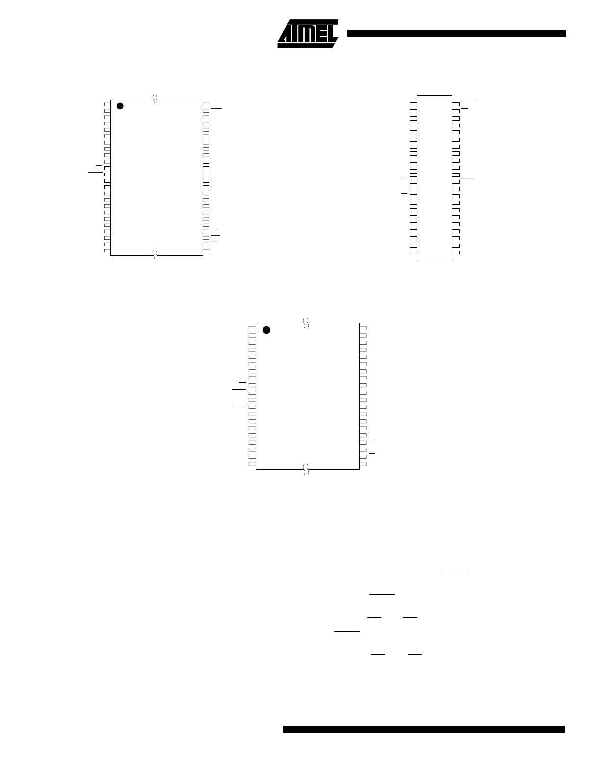
AT49F8192A(T) TSOP Top View
Typ e 1
A15
A14
A13
A12
A11
A10
RESET
A18
A17
1
2
3
4
5
6
7
A9
8
A8
9
NC
10
NC
11
WE
12
13
NC
14
NC
15
NC
16
17
18
A7
19
A6
20
A5
21
A4
22
A3
23
A2
24
A1
48
47
46
45
44
43
42
41
40
39
38
37
36
35
34
33
32
31
30
29
28
27
26
25
A16
BYTE
GND
I/O15 / A-1
I/O7
I/O14
I/O6
I/O13
I/O5
I/O12
I/O4
VCC
I/O11
I/O3
I/O10
I/O2
I/O9
I/O1
I/O8
I/O0
OE
GND
CE
A0
AT49F008A(T) TSOP Top View
Type 1
1
A16
2
A15
3
A14
4
A13
5
A12
6
A11
7
A9
8
A8
9
WE
10
RESET
11
NC
A18
12
13
14
A7
15
A6
16
A5
17
A4
18
A3
19
A2
20
A1
RDY/BUSY
AT49F8192A(T) SOIC (SOP) Top View
1
44
NC
2
A18
3
A17
4
A7
5
A6
6
A5
7
A4
8
A3
9
A2
10
A1
11
A0
12
CE
13
GND
14
OE
15
I/O0
16
I/O8
17
I/O1
18
I/O9
19
I/O2
20
I/O10
21
I/O3
22
I/O11
40
A17
39
GND
38
NC
37
A-1
36
A10
35
I/O7
34
I/O6
33
I/O5
32
I/O4
31
VCC
30
VCC
29
NC
28
I/O3
27
I/O2
26
I/O1
25
I/O0
24
OE
23
GND
22
CE
21
A0
RESET
43
WE
42
A8
41
A9
40
A10
39
A11
38
A12
37
A13
36
A14
35
A15
34
A16
33
BYTE
32
GND
31
I/O15
30
I/O7
29
I/O14
28
I/O6
27
I/O13
26
I/O5
25
I/O12
24
I/O4
23
VCC
Note: “•” denotes a white dot marked on the package.
The device is erased by executing the Erase command
sequence; the device internally controls the erase operation. The memory is divided into four blocks for erase operations. There are two 4K word parameter block sections:
the boot block, and the main memory array block. The typical number of program and erase cycles is in excess of
10,000 cycles.
The optional 8K word boot block section includes a reprogramming lockout feature to provide data integrity. This
feature is enabled by a command sequence. Once the boot
block programming lockout feature is enabled, the data in
the boot block cannot be changed when input levels of 5.5
2
AT49F008A(T)/8192A(T)
volts or less are used. The boot sector is designed to contain user secure code.
For the AT49F8192A(T), the BYTE
pin controls whether
the device data I/O pins operate in the byte or word configuration. If the BYTE
pin is set at a logic “1” or left open, the
device is in word configuration, I/O0 - I/O15 are active and
controlled by CE
If the BYTE
and OE.
pin is set at logic “0”, the device is in byte configuration, and only data I/O pins I/O0 - I/O7 are active and
controlled by CE
and OE. The data I/O pins I/O8 - I/O14
are tri-stated and the I/O15 pin is used as an input for the
LSB (A-1) address function.
1199F–04/01
Page 3
AT49F008A(T) Block Diagram
VCC
GND
OE
WE
CE
CONTROL
LOGIC
RESET
ADDRESS
INPUTS
Y DECODER
X DECODER
AT49F8192A(T) Block Diagram
VCC
GND
AT49F008A AT49F008AT
DATA INPUTS/OUTPUTS
I/O0 - I/O7
INPUT/OUTPUT
BUFFERS
PROGRAM DATA
LATCHES
Y-GATING
MAIN MEMORY
(992K BYTES)
PARAMETER
BLOCK 2
8K BYTES
PARAMETER
BLOCK 1
8K BYTES
BOOT BLOCK
16K BYTES
AT49F8192A AT49F8192AT
DATA INPUTS/OUTPUTS
I/O0 - I/O15
AT49F008A(T)/8192A(T)
DATA INPUTS/OUTPUTS
I/O0 - I/O7
INPUT/OUTPUT
BUFFERS
PROGRAM DATA
LATCHES
FFFFF FFFFF
08000
07FFF
06000
05FFF
04000
03FFF
00000 00000
DATA INPUTS/OUTPUTS
Y-GATING
BOOT BLOCK
16K BYTES
PARAMETER
BLOCK 1
8K BYTES
PARAMETER
BLOCK 2
8K BYTES
MAIN MEMORY
(992K BYTES)
I/O0 - I/O15
FC000
FBFFF
FA000
F9FFF
F8000
F7FFF
OE
WE
CE
RESET
ADDRESS
INPUTS
CONTROL
LOGIC
Y DECODER
X DECODER
INPUT/OUTPUT
BUFFERS
PROGRAM DATA
LATCHES
Y-GATING
MAIN MEMORY
(496K WORDS)
PARAMETER
BLOCK 2
4K WORDS
PARAMETER
BLOCK 1
4K WORDS
BOOT BLOCK
8K WORDS
INPUT/OUTPUT
BUFFERS
PROGRAM DATA
LATCHES
7FFFF 7FFFF
04000
03FFF
03000
02FFF
02000
01FFF
00000 00000
Y-GATING
BOOT BLOCK
8K WORDS
PARAMETER
BLOCK 1
4K WORDS
PARAMETER
BLOCK 2
4K WORDS
MAIN MEMORY
(496K WORDS)
7E000
7DFFF
7D000
7CFFF
7C000
7BFFF
Device Operation
READ: The AT49F008A(T)/8192A(T) is accessed like an EPROM. When CE and OE are low and WE is high, the data
stored at the memory location determined by the address pins is asserted on the outputs. The outputs are put in the highimpedance state whenever CE
COMMAND SEQUENCES: When the device is first powered on, it will be reset to the read or standby mode, depending
upon the state of the control line inputs. In order to perform other device functions, a series of command sequences are
entered into the device. The command sequences are shown in the Command Definitions table (I/O8 - I/O15 are don’t care
inputs for the command codes). The command sequences are written by applying a low pulse on the WE
or WE low (respectively) and OE high. The address is latched on the falling edge of CE or WE, whichever occurs last.
CE
The data is latched by the first rising edge of CE
locations used in the command sequences are not affected by entering the command sequences.
or OE is high. This dual line control gives designers flexibility in preventing bus contention.
or CE input with
or WE. Standard microprocessor write timings are used. The address
1199F–04/01
3
Page 4

RESET: A RESET input pin is provided to ease some sys-
tem applications. When RESET
device is in its standard operating mode. A low level on the
RESET
the outputs of the device in a high-impedance state. When
a high level is reasserted on the RESET
returns to the read or standby mode, depending upon the
state of the control inputs. By applying a 12V ± 0.5V input
signal to the RESET
grammed even if the boot block program lockout feature
has been enabled (see Boot Block Programming Lockout
Override section).
ERASURE: Before a byte or word can be reprogrammed, it
must be erased. The erased state of memory bits is a logic
“1”. The entire device can be erased by using the Chip
Erase command or individual sectors can be erased by
using the Sector Erase command.
CHIP ERASE: The entire device can be erased at one time
by using the 6-byte chip erase software code. After the chip
erase has been initiated, the device will internally time the
erase operation so that no external clocks are required.
The maximum time to erase the chip is t
If the boot block lockout has been enabled, the chip erase
will not erase the data in the boot block; it will erase the
main memory block and the parameter blocks only. After
the chip erase, the device will return to the read or standby
mode.
SECTOR ERASE: As an alternative to a full chip erase, the
device is organized into four sectors that can be individually
erased. There are two 4K word parameter block sections,
one boot block, and the main memory array block. The
Sector Erase command is a six-bus cycle operation. The
sector address is latched on the falling WE
sixth cycle while the 30H data input command is latched at
the rising edge of WE
rising edge of WE
internally controlled; it will automatically time to completion.
Whenever the main memory block is erased and reprogrammed, the two parameter blocks should be erased and
reprogrammed before the main memory block is erased
again. Whenever a parameter block is erased and reprogrammed, the other parameter block should be erased and
reprogrammed before the first parameter block is erased
again. Whenever the boot block is erased and reprogrammed, the main memory block and the parameter
blocks should be erased and reprogrammed before the
boot block is erased again.
BYTE/WORD PROGRAMMING: Once a memory block is
erased, it is programmed (to a logic “0”) on a byte-by-byte
or word-by-word basis. Programming is accomplished via
the internal device command register and is a four-bus
cycle operation. The device will automatically generate the
required internal program pulses.
input halts the present device operation and puts
pin, the boot block array can be repro-
. The sector erase starts after the
of the sixth cycle. The erase operation is
is at a logic high level, the
pin, the device
.
EC
edge of the
Any commands written to the chip during the embedded
programming cycle will be ignored. If a hardware reset
happens during programming, the data at the location
being programmed will be corrupted. Please note that a
data “0” cannot be programmed back to a “1”; only erase
operations can convert “0”s to “1”s. Programming is completed after the specified t
feature may also be used to indicate the end of a program
cycle.
BOOT BLOCK PROGRAMMING LOCKOUT: The device
has one designated block that has a programming lockout
feature. This feature prevents programming of data in the
designated block once the feature has been enabled. The
size of the block is 8K words. This block, referred to as the
boot block, can contain secure code that is used to bring up
the system. Enabling the lockout feature will allow the boot
code to stay in the device while data in the rest of the
device is updated. This feature does not have to be activated; the boot block’s usage as a write-protected region is
optional to the user. The address range of the boot block is
00000H to 03FFFH for the AT49F008A; FC000H to
FFFFFH for the AT49F008AT; 00000H to 01FFFH for the
AT49F8192A; and 7E000H to 7FFFFH for the
AT49F8192AT.
Once the feature is enabled, the data in the boot block can
no longer be erased or programmed when input levels of
5.5V or less are used. Data in the main memory block can
still be changed through the regular programming method.
To activate the lockout feature, a series of six program
commands to specific addresses with specific data must be
performed. Please refer to the Command Definitions table.
BOOT BLOCK LOCKOUT DETECTION: A software
method is available to determine if programming of the boot
block section is locked out. When the device is in the software product identification mode (see Software Product
Identification Entry and Exit sections), a read from the
following address location will show if programming the
boot block is locked out – 00002H for the AT49F008A and
AT49F8192A; FC002H for the AT49F008AT; and 7E002H
for the AT49F8192AT. If the data on I/O0 is low, the boot
block can be programmed; if the data on I/O0 is high, the
program lockout feature has been enabled and the block
cannot be programmed. The software product identification
exit code should be used to return to standard operation.
BOOT BLOCK PROGRAMMING LOCKOUT OVERRIDE:
The user can override the boot block programming lockout
by taking the RESET
erase, sector erase or word programming operation. When
the RESET
block programming lockout feature is again active.
PRODUCT IDENTIFICATION: The product identification
mode identifies the device and manufacturer as Atmel. It
may be accessed by hardware or software operation. The
pin is brought back to TTL levels, the boot
pin to 12 volts during the entire chip
cycle time. The Data Polling
BP
4
AT49F008A(T)/8192A(T)
1199F–04/01
Page 5

AT49F008A(T)/8192A(T)
hardware operation mode can be used by an external programmer to identify the correct programming algorithm for the
Atmel product.
For details, see “Operating Modes” (for hardware operation) or “Software Product Identification Entry/Exit” on page 12. The
manufacturer and device codes are the same for both modes.
DATA
POLLING: The AT49F008A(T)/8192A(T) features Data Polling to indicate the end of a program cycle. During a pro-
gram cycle an attempted read of the last byte loaded will result in the complement of the loaded data on I/O7. Once the program cycle has been completed, true data is valid on all outputs and the next cycle may begin. During a chip or sector
erase operation, an attempt to read the device will give a “0” on I/O7. Once the program or erase cycle has completed, true
data will be read from the device. Data
TOGGLE BIT: In addition to Data
a program or erase cycle. During a program or erase operation, successive attempts to read data from the device will result
in I/O6 toggling between one and zero. Once the program cycle has completed, I/O6 will stop toggling and valid data will be
read. Examining the toggle bit may begin at any time during a program cycle.
READY/BUSY
detecting the end of a program or erase operation. RDY/BUSY
cycles and it is released at the completion of the cycle. The open-drain connection allows for OR-tying of several devices to
the same RDY/BUSY
HARDWARE DATA PROTECTION: Hardware features protect against inadvertent programs to the
AT49F008A(T)/8192A(T) in the following ways: (a) V
ited. (b) V
cal) before programming. (c) Program inhibit: holding any one of OE
Noise filter: pulses of less than 15 ns (typical) on the WE
: For the AT49F008A(T), pin 12 is an open-drain Ready/Busy output pin, which provides another method of
line.
power-on delay: once VCC has reached the VCC sense level, the device will automatically time-out 10 ms (typi-
CC
Polling may begin at any time during the program cycle.
Polling, the AT49F008A(T)/8192A(T) provides another method for determining the end of
is actively pulled low during the internal program and erase
sense: if VCC is below 3.8V (typical), the program function is inhib-
CC
low, CE high or WE high inhibits program cycles. (d)
or CE inputs will not initiate a program cycle.
1199F–04/01
5
Page 6

Command Definition in Hex
Command
Sequence
Read 1 Addr D
Chip Erase 6 5555 AA 2AAA 55 5555 80 5555 AA 2AAA 55 5555 10
Sector Erase 6 5555 AA 2AAA 55 5555 80 5555 AA 2AAA 55 SA
Byte/Word Program 4 5555 AA 2AAA 55 5555 A0 Addr D
Boot Block Lockout
Product ID Entry 3 5555 AA 2AAA 55 5555 90
Product ID Exit
Product ID Exit
Notes: 1. The DATA FORMAT in each bus cycle is as follows: I/O15 - I/O8 (Don’t Care); I/O7 - I/O0 (Hex).
(3)
(3)
The ADDRESS FORMAT in each bus cycle is as follows: A15 - A0 (Hex); A-1 and A15 - A18 (Don’t Care).
2. The boot sector has the address range
AT49F008AT; 00000H to 01FFFH for the AT49F8192A; and 7E000H to 7FFFFH for the AT49F8192AT
3. Either one of the Product ID Exit commands can be used.
4. SA = sector addresses: (A0 - A18)
For the AT49F008A/8192A
SA = 01XXX for BOOT BLOCK
SA = 02XXX for PARAMETER BLOCK 1
SA = 03XXX for PARAMETER BLOCK 2
SA = 7FXXX for MAIN MEMORY ARRAY
Bus
Cycles
(2)
Addr Data Addr Data Addr Data Addr Data Addr Data Addr Data
6 5555 AA 2AAA 55 5555 80 5555 AA 2AAA 55 5555 40
3 5555 AA 2AAA 55 5555 F0
1xxxxF0
(1)
1st Bus
Cycle
2nd Bus
Cycle
OUT
3rd Bus
Cycle
4th Bus
Cycle
5th Bus
Cycle
IN
00000H to 03FFFH for the AT49F008A; FC000H to FFFFFH for the
6th Bus
Cycle
(4)
.
30
For the AT49F008AT/8192AT
SA = 7FXXX for BOOT BLOCK
SA = 7DXXX for PARAMETER BLOCK 1
SA = 7CXXX for PARAMETER BLOCK 2
SA = 7BXXX for MAIN MEMORY ARRAY
Absolute Maximum Ratings*
Temperature under Bias ................................ -55°C to +125°C
Storage Temperature ..................................... -65°C to +150°C
All Input Voltages
(including NC Pins)
with Respect to Ground...................................-0.6V to +6.25V
All Output Voltages
with Respect to Ground.............................-0.6V to V
Voltage on RESET
with Respect to Ground...................................-0.6V to +13.5V
+ 0.6V
CC
*NOTICE: Stresses beyond those listed under “Absolute
Maximum Ratings” may cause permanent damage to the device. This is a stress rating only and
functional operation of the device at these or any
other conditions beyond those indicated in the
operational sections of this specification is not
implied. Exposure to absolute maximum rating
conditions for extended periods may affect device
reliability.
6
AT49F008A(T)/8192A(T)
1199F–04/01
Page 7

AT49F008A(T)/8192A(T)
DC and AC Operating Range
AT49F008A/8192A(T)-90
(3)
H
(3)
H
IL
IL
°C - 70°C
°C - 85°C
Operating Temperature (Case)
Com. 0
Ind. -40
Power Supply 5V ± 10%
V
CC
Operating Modes
Mode CE OE WE RESET Ai I/O
Read V
Program/Erase
(2)
Standby/Program
Inhibit
IL
V
IL
V
IH
V
IL
V
IH
(1)
X
Program Inhibit X X V
Program Inhibit X V
Output Disable X V
IL
IH
Reset X X X V
Product Identification
Hardware V
Software
(5)
IL
V
IL
Notes: 1. X can be VIL or VIH.
2. Refer to AC programming waveforms.
3. VH = 12.0V ± 0.5V.
4. Manufacturer Code: 001FH
Device Code: 22H (AT49F008A); 00A0H (AT49F8192A); 21H (AT49F008AT); 00A3H (AT49F8192AT).
5. See details under “Software Product Identification Entry/Exit” on page 12.
V
IH
V
IL
XV
IH
XV
XV
V
IH
V
IH
V
IH
IH
V
IH
IH
IH
IL
V
IH
V
IH
Ai D
Ai D
X High-Z
X High-Z
A1 - A18 = VIL, A9 = V
A0 = V
IL
A1 - A18 = VIL, A9 = V
A0 = V
IH
A0 = VIL, A1 - A18 = V
A0 = VIH, A1 - A18 = V
OUT
IN
High-Z
Manufacturer Code
Device Code
(4)
Manufacturer Code
Device Code
(4)
(4)
(4)
DC Characteristics
Symbol Parameter Condition Min Max Units
I
I
I
I
I
V
V
V
V
LI
LO
SB1
SB2
CC
(1)
IL
IH
OL
OH
Input Load Current VIN = 0V to V
Output Leakage Current V
VCC Standby Current CMOS CE = VCC - 0.3V to V
VCC Standby Current TTL CE = 2.0V to V
V
Active Current f = 5 MHz; I
CC
Input Low Voltage 0.8 V
Input High Voltage 2.0 V
Output Low Voltage IOL = 2.1 mA 0.45 V
Output High Voltage IOH = -400 µA 2.4 V
Note: 1. In the erase mode, I
is 90 mA.
CC
= 0V to V
I/O
CC
CC
CC
CC
= 0 mA 50.0 mA
OUT
10.0 µA
10.0 µA
100.0 µA
3.0 mA
1199F–04/01
7
Page 8

AC Read Characteristics
Symbol Parameter
t
t
t
t
t
t
ACC
CE
OE
DF
OH
RO
(1)
(2)
(3)(4)
Address to
Output Delay
CE to Output Delay 90 ns
OE to Output Delay 0 40 ns
CE or OE to Output Float 0 25 ns
Output Hold from OE, CE or Address, whichever occurred first 0 ns
RESET to Output Delay 800 ns
AT49F008A/8192A(T)-90
UnitsMin Max
90 ns
AC Read Waveforms
Notes: 1. CE may be delayed up to t
(1)(2)(3)(4)
ADDRESS
CE
OE
RESET
OUTPUT
- tCE after the address transition without impact on t
ACC
ADDRESS VALID
t
ACC
t
RO
HIGH Z
t
CE
t
OE
2. OE may be delayed up to tCE - tOE after the falling edge of CE without impact on tCE or by t
without impact on t
is specified from OE or CE, whichever occurs first (CL = 5 pF).
3. t
DF
ACC
.
4. This parameter is characterized and is not 100% tested.
Input Test Waveforms and Measurement Level
OUTPUT
VALID
t
DF
t
OH
.
ACC
- tOE after an address change
ACC
Output Test Load
3.0V
0.0V
tR, tF < 5 ns
Pin Capacitance
f = 1 MHz, T = 25° C
C
IN
C
OUT
Note: 1. This parameter is characterized and is not 100% tested.
8
AT49F008A(T)/8192A(T)
(1)
Typ Max Units Conditions
46 pFV
812 pFV
IN
OUT
5.0V
= 0V
= 0V
1199F–04/01
Page 9

AT49F008A(T)/8192A(T)
AC Word Load Characteristics
Symbol Parameter Min Max Units
tAS, t
t
AH
t
CS
t
CH
t
WP
t
DS
tDH, t
t
WPH
AC Byte/Word Load Waveforms
WE Controlled
Address, OE Setup Time 0 ns
OES
Address Hold Time 50 ns
Chip Select Setup Time 0 ns
Chip Select Hold Time 0 ns
Write Pulse Width (WE or CE)50ns
Data Setup Time 50 ns
Data, OE Hold Time 0ns
OEH
Write Pulse Width High 40 ns
Controlled
CE
1199F–04/01
9
Page 10

Program Cycle Characteristics
Symbol Parameter Min Typ Max Units
t
BP
t
AS
t
AH
t
DS
t
DH
t
WP
t
WPH
t
EC
Program Cycle Waveforms
Byte/Word Programming Time 10 50 µs
Address Setup Time 0 ns
Address Hold Time 50 ns
Data Setup Time 50 ns
Data Hold Time 0 ns
Write Pulse Width 50 ns
Write Pulse Width High 40 ns
Erase Cycle Time 5 seconds
PROGRAM CYCLE
OE
CE
t
WP
WE
t
DH
2AAA
t
DS
55
A0-A18
DATA
t
AS
t
AH
5555 5555
AA
Sector or Chip Erase Cycle Waveforms
(1)
OE
CE
WE
A0-A18
DATA
t
WP
t
AS
5555
t
AH
AA
BYTE/
WORD 0
t
DH
2AAA 2AAA
t
DS
55 55
BYTE/
WORD 1
t
5555
WPH
WORD 2
80
BYTE/
t
WPH
A0
5555
ADDRESS
AA
BYTE/
WORD 3
INPUT DATA
WORD 4
BYTE/
t
Note 2
BP
Note 3
BYTE/
WORD 5
5555
AA
t
EC
Notes: 1. OE must be high only when WE and CE are both low.
2. For chip erase, the address should be 5555. For sector erase, the address depends on what sector is to be erased.
(See note 4 under Command Definitions.)
3. For chip erase, the data should be 10H, and for sector erase, the data should be 30H.
10
AT49F008A(T)/8192A(T)
1199F–04/01
Page 11

AT49F008A(T)/8192A(T)
Data Polling Characteristics
(1)
Symbol Parameter Min Typ Max Units
t
DH
t
OEH
t
OE
t
WR
Data Hold Time 10 ns
OE Hold Time 10 ns
OE to Output Delay
(2)
Write Recovery Time 0 ns
Notes: 1. These parameters are characterized and not 100% tested.
2. See t
spec in “AC Read Characteristics” on page 8.
OE
Data Polling Waveforms
ns
Toggle Bit Characteristics
(1)
Symbol Parameter Min Typ Max Units
t
DH
t
OEH
t
OE
t
OEHP
t
WR
Data Hold Time 10 ns
OE Hold Time 10 ns
OE to Output Delay
(2)
OE High Pulse 150 ns
Write Recovery Time 0 ns
Notes: 1. These parameters are characterized and not 100% tested.
2. See t
Toggle Bit Waveforms
spec in “AC Read Characteristics” on page 8.
OE
(1)(2)(3)
ns
Notes: 1. Toggling either OE or CE or both OE and CE will operate toggle bit. The t
input(s).
2. Beginning and ending state of I/O6 will vary.
3. Any address location may be used but the address should not vary.
1199F–04/01
specification must be met by the toggling
OEHP
11
Page 12

Software Product Identification Entry
LOAD DATA AA
TO
TO
TO
OR
(2)(3)(5)
(7)
(7)
(7)
LOAD DATA F0
ANY ADDRESS
EXIT PRODUCT
IDENTIFICATION
MODE
(1)(6)
TO
(4)
ADDRESS 5555
LOAD DATA 55
ADDRESS 2AAA
LOAD DATA 90
ADDRESS 5555
ENTER PRODUCT
IDENTIFICATION
MODE
Software Product Identification Exit
LOAD DATA AA
TO
TO
(7)
(7)
ADDRESS 5555
LOAD DATA 55
ADDRESS 2AAA
(1)
Boot Block Lockout Enable
Algorithm
(1)
LOAD DATA AA
TO
ADDRESS 5555
LOAD DATA 55
TO
ADDRESS 2AAA
LOAD DATA 80
TO
ADDRESS 5555
LOAD DATA AA
TO
ADDRESS 5555
LOAD DATA 55
TO
ADDRESS 2AAA
LOAD DATA 40
TO
ADDRESS 5555
(3)
(3)
(3)
(3)
(3)
(3)
LOAD DATA F0
TO
ADDRESS 5555
EXIT PRODUCT
IDENTIFICATION
MODE
(7)
(4)
Notes: 1. Data Format: I/O15 - I/O8 (Don’t Care); I/O7 - I/O0 (Hex).
Address Format: A15 - A0 (Hex); A-1 and A15 - A18 (Don’t
Care).
2. A1 - A18 = V
Manufacturer Code is read for A0 = V
Device Code is read for A0 = V
.
IL
.
IL
.
IH
3. The device does not remain in identification mode if
powered down.
4. The device returns to standard operation mode.
5. Manufacturer Code: 001FH
Device Code: 22H (AT49F008A); 00A0H (AT49F8192A);
21H (AT49F008AT); 00A3H (AT49F8192AT)
6. Either one of the Product ID Exit commands can be used.
PAUSE 1 second
(2)
Notes: 1. Data Format: I/O15 - I/O8 (Don’t Care); I/O7 - I/O0 (Hex).
Address Format: A15 - A0 (Hex); A-1 and A15 - A18 (Don’t
Care).
2. Boot Block Lockout feature enabled.
12
AT49F008A(T)/8192A(T)
1199F–04/01
Page 13

AT49F008A(T)/8192A(T)
AT49F008A Ordering Information
I
(mA)
t
ACC
(ns)
90 50 0.3 AT49F008A-90TI 40T Industrial
AT49F8192A(T) Ordering Information
t
ACC
(ns)
90 50 0.3 AT49F8192A-90TC 48T Commercial
90 50 0.3 AT49F8192AT-90RC
CC
I
CC
(mA)
Standby
Ordering Code Package Operation RangeActive
Ordering Code Package Operation RangeActive Standby
AT49F8192AT-90TC
44R
48T
(-40° to 85°C)
(0° to 70°C)
Commercial
(0° to 70°C)
Package Type
44R 44-lead, 0.525" Wide, Plastic Gull Wing Small Outline Package (SOIC)
40T 40-lead, Plastic Thin Small Outline Package (TSOP)
48T 48-lead, Plastic Thin Small Outline Package (TSOP)
1199F–04/01
13
Page 14

Packaging Information
44R, 44-lead, 0.525" Wide, Plastic Gull Wing Small
Outline Package (SOIC)
Dimensions in Inches and (Millimeters)
40T, 40-lead, Plastic Thin Small Outline Package
(TSOP)
Dimensions in Inches and (Millimeters)*
48T, 48-lead, Plastic Thin Small Outline Package
(TSOP)
Dimensions in Millimeters and (Inches)*
JEDEC OUTLINE MO-142 D
*Controlling dimension: millimeters
*Controlling dimension: millimeters
14
AT49F008A(T)/8192A(T)
1199F–04/01
Page 15

Atmel Headquarters Atmel Operations
Corporate Headquarters
2325 Orchard Parkway
San Jose, CA 95131
TEL (408) 441-0311
FAX (408) 487-2600
Europe
Atmel SarL
Route des Arsenaux 41
Casa Postale 80
CH-1705 Fribourg
Switzerland
TEL (41) 26-426-5555
FAX (41) 26-426-5500
Asia
Atmel Asia, Ltd.
Room 1219
Chinachem Golden Plaza
77 Mody Road Tsimhatsui
East Kowloon
Hong Kong
TEL (852) 2721-9778
FAX (852) 2722-1369
Japan
Atmel Japan K.K.
9F, Tonetsu Shinkawa Bldg.
1-24-8 Shinkawa
Chuo-ku, Tokyo 104-0033
Japan
TEL (81) 3-3523-3551
FAX (81) 3-3523-7581
Atmel Colorado Springs
1150 E. Cheyenne Mtn. Blvd.
Colorado Springs, CO 80906
TEL (719) 576-3300
FAX (719) 540-1759
Atmel Rousset
Zone Industrielle
13106 Rousset Cedex
France
TEL (33) 4-4253-6000
FAX (33) 4-4253-6001
Atmel Smart Card ICs
Scottish Enterprise Technology Park
East Kilbride, Scotland G75 0QR
TEL (44) 1355-357-000
FAX (44) 1355-242-743
Atmel Grenoble
Avenue de Rochepleine
BP 123
38521 Saint-Egreve Cedex
France
TEL (33) 4-7658-3000
FAX (33) 4-7658-3480
Fax-on-Demand
North America:
e-mail
literature@atmel.com
1-(800) 292-8635
International:
1-(408) 441-0732
Web Site
http://www.atmel.com
BBS
1-(408) 436-4309
© Atmel Corporation 2001.
Atmel Corporation makes no warranty for the use of its products, other than those expressly contained in the Company’s standard warranty
which is detailed in Atmel’s Terms and Conditions located on the Company’s web site. The Company assumes no responsibility for any errors
which may appear in this document, reserves the right to change devices or specifications detailed herein at any time without notice, and does
not make any commitment to update the information contained herein. No licenses to patents or other intellectual property of Atmel are granted
by the Company in connection with the sale of Atmel products, expressly or by implication. Atmel’s products are not authorized for use as critical
components in life support devices or systems.
AT ME L®, Cache Logic®, AVR Studio® are the registered trademarks of Atmel Corporation; FPSLIC, FreeRAM
and HDLPlanner are the trademarks of Atmel Corporation.
Other terms and product names may be the trademark of others.
Printed on recycled paper.
1199F–04/01/xM
 Loading...