

Page 1
Features
5
6
7
8
9
10
11
12
13
29
28
27
26
25
24
23
22
21
A7
A6
A5
A4
A3
A2
A1
A0
I/O0
A14
A13
A8
A9
A11
OE
A10
CE
I/O7
432
1
323130
14151617181920
I/O1
I/O2
GND
I/O3
I/O4
I/O5
I/O6
A12
A15
A16
RESET *
VCCWEA17
• Single-voltage Operation
–5V Read
– 5V Reprogramming
• Fast Read Access Time - 55 ns
• Internal Program Control and Timer
• Sector Architecture
– One 16K Byte Boot Block with Programming Lockout
– Two 8K Byte Parameter Blocks
– Two Main Memory Blocks (96K, 128K Bytes)
• Fast Erase Cycle Time - 10 seconds
• Byte-by-byte Programming - 10 µs/Byte Typical
• Hardware Data Protection
• DAT A Polling for End of Program Detection
• Low Power Dissipation
– 50 mA Active Current
– 100 µA CMOS Standby Current
• Typical 10,000 Write Cycles
Description
The AT49F002(N)(T) is a 5-volt only in-system reprogrammable Flash memory. Its 2
megabits of memory is orga nized as 262,144 words by 8 bits. Manufactured with
Atmel’s advanced nonvolatile CMOS technology, the device offers access times to 55
ns with power dissipation of just 275 mW over the commercial temperature range.
(continued)
2-megabit
(256K x 8)
5-volt Only
Flash Memory
AT49F002
AT49F002N
AT49F002T
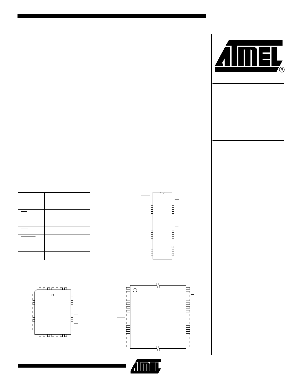
Pin Configurations
Pin Name Function
A0 - A17 Addresses
CE
OE
WE Write Enable
RESET
I/O0 - I/O7 Data Inputs/Outputs
DC Don’t Connect
*Note: This pin is a DC on the AT49F002(N)(T).
Chip Enable
Output Enable
RESET
PLCC Top View
DIP Top View
1
* RESET
2
A16
3
A15
4
A12
5
A7
6
A6
7
A5
8
A4
9
A3
10
A2
11
A1
12
A0
13
I/O0
14
I/O1
15
I/O2
16
GND
VSOP Top View (8 x 14 mm) or
TSOP Top View (8 x 20 mm)
Type 1
1
A11
2
A9
3
A8
4
A13
5
A14
6
A17
7
WE
8
VCC
A16
A15
A12
9
10
11
12
13
A7
14
A6
15
A5
16
A4
* RESET
AT49F002NT
VCC
32
WE
31
A17
30
A14
29
A13
28
A8
27
A9
26
A11
25
OE
24
A10
23
CE
22
I/O7
21
I/O6
20
I/O5
19
I/O4
18
I/O3
17
OE
32
A10
31
CE
30
I/O7
29
I/O6
28
I/O5
27
I/O4
26
I/O3
25
GND
24
I/O2
23
I/O1
22
I/O0
21
A0
20
A1
19
A2
18
A3
17
Rev. 1017D–10/99
1
Page 2
When the device is dese lecte d, the CMO S stan dby cu rrent
is less than 100 µA. For the AT49F002N(T) pin 1 for the
DIP and PLCC packages and pin 9 for the TSOP package
are don’t connect pins.
To allow for simple in-system reprogrammability, the
AT49F002(N)(T) does not require high input voltages for
programming. Five-volt-only commands determine the read
and programming operation o f the device. Readin g data
out of the device is similar to reading from an EPROM; it
has standard CE
, OE, and WE inputs to avoid bu s conten tion. Reprogramming the AT49F002(N)(T) is performed by
erasing a block of data and then programming on a byte by
byte basis. The byte pr ogram ming time is a fast 50 µs. The
end of a program cycle can be optionally detected by the
polling feature. Once the end of a byte program
DATA
cycle has been detected, a new access for a read or program can begin. The typical nu mber of pr ogram a nd erase
cycles is in excess of 10,000 cycles.
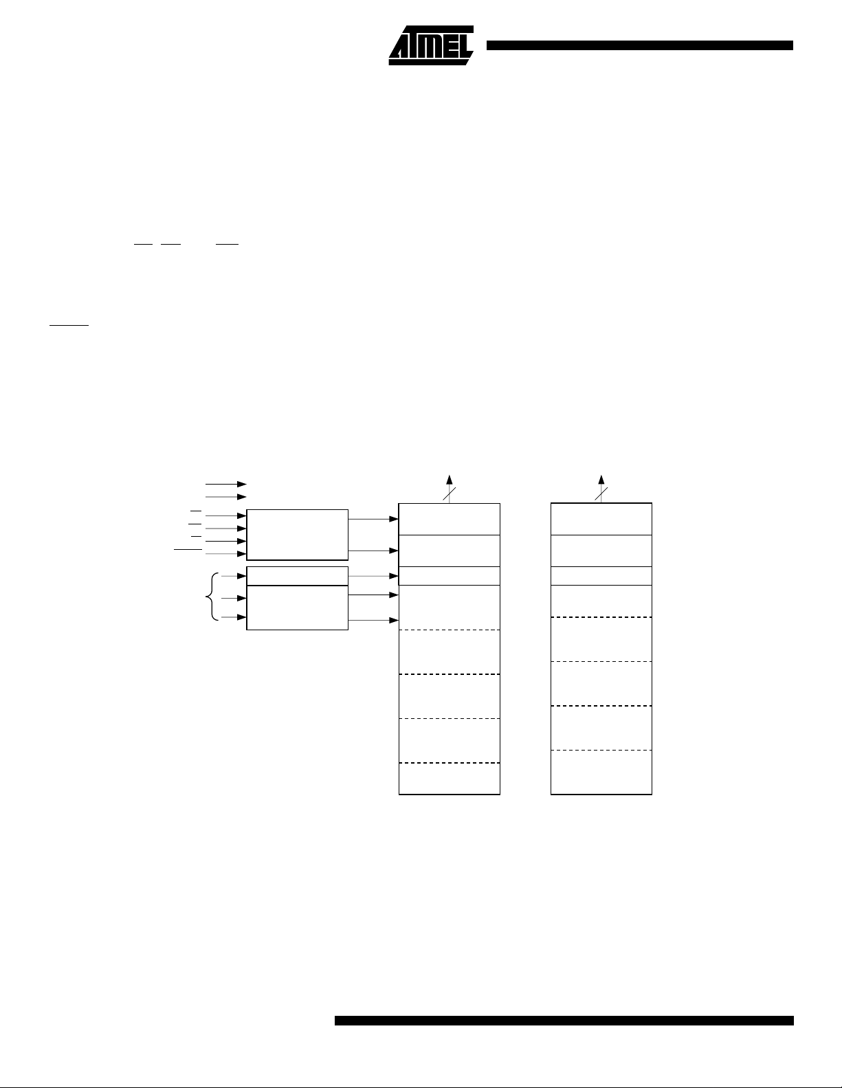
Block Diagram
VCC
GND
OE
WE
CE
RESET
ADDRESS
INPUTS
CONTROL
LOGIC
Y DECODER
X DECODER
The device is erased by executing the er ase command
sequence; the device internally controls the erase operations. There are two 8K byte para meter bloc k sectio ns and
two main memory blocks.
The device has the capability to protect the data in the boot
block; this feature is enabled by a command sequence.
The 16K-byte boot block section includes a reprogramming
lock out feature to prov ide data in tegr i ty. The boot sector is
designed to contai n user secur e code, and when the feature is enabled, the boot sector is protected from being
reprogrammed.
In the AT49F002(N)(T), once the boot block programming
lockout feature is enabled, the contents of the boot block
are permanent and cannot be changed. In the
AT49F002(T), once the boot block programm ing lockout
feature is enabled, the contents of the boot block cannot be
changed with input voltage levels of 5.5 volts or less.
AT49F002(N)
DATA INPUTS/OUTPUTS
I/O7 - I/O0
8
INPUT/OUTPUT
BUFFERS
PROGRAM
DATA LATCHES
Y-GATING
MAIN MEMORY
BLOCK 2
(128K BYTES)
MAIN MEMORY
BLOCK 1
(96K BYTES)
PARAMETER
BLOCK 2
(8K BYTES)
PARAMETER
BLOCK 1
(8K BYTES)
BOOT BLOCK
(16K BYTES)
3FFFF
20000
1FFFF
08000
07FFF
06000
05FFF
04000
03FFF
00000
AT49F002(N)T
DATA INPUTS/OUTPUTS
I/O7 - I/O0
8
INPUT/OUTPUT
BUFFERS
PROGRAM
DATA LATCHES
Y-GATING
BOOT BLOCK
(16K BYTES)
PARAMETER
BLOCK 1
(8K BYTES)
PARAMETER
BLOCK 2
(8K BYTES)
MAIN MEMORY
BLOCK 1
(96K BYTES)
MAIN MEMORY
BLOCK 2
(128K BYTES)
3FFFF
3C000
3BFFF
3A000
39FFF
38000
37FFF
20000
1FFFF
00000
2
AT49F002(N)(T)
Page 3

Device Operation
READ: The AT49F002(N)(T) is accessed like an EPROM.
When CE
at the memory location determined by the address pins is
asserted on the outputs. The outputs are put in the high
impedance state whenever CE
control gives designers flexibility in preventing bus contention.
COMMAND SEQUENCES: When th e device is first p owered on it will be reset to the read or standby mode
depending upon the state of the control line inputs. In order
to perform other device functions, a series of command
sequences are entered into the device. The command
sequences are shown in the Command Definitions table.
The command sequences are written by applying a low
pulse on the WE
tively) and OE
edge of CE
latched by the first rising edge of CE
microprocessor write timings are used. The address locations used in the command sequences are not affected by
entering the command sequences.
RESET: A RESET
tem application s. When RE SET
device is in its standa rd oper at ing mod e. A low l evel on th e
RESET
the outputs of the device in a high impedance state. If the
RESET
or erase operation, the operation may not be successfully
completed and the op eratio n will have to be repeate d after
a high level is applied to the RESET
is reasserted on the RESET
read or standby mode, depending upon the state of the
control inputs. By ap plyi ng a 12 V
RESET
even if the boot block loc kout feature has be en enabled
(see Boot Bloc k Prog ramming Locko ut Over ride s ection) .
The RESET feature is not available for the AT49F002N(T).
ERASURE: Before a byte can be repr ogramme d, the main
memory block or parameter block which contains the byte
must be erased. The erased state of the memor y bits is a
logical “1”. The entire devic e can be eras ed at one tim e by
using a 6-byte soft ware code. T he software chip erase
code consists of 6-byte load commands to specific address
locations with a specific data pattern (please refer to the
Chip Erase Cycle Waveforms).
After the software c hi p e ra se has been initiate d, the d evi ce
will internally time the er ase operation so that no e xternal
clocks are required. The maximum time needed to erase
the whole chip is t
been enabled, the data in the boot sector will not be
erased.
and OE are low and WE is high, the data stored
or OE is high. This dual-line
or CE input with CE or WE low (respec-
high. The address is latched on the falling
or WE, whichever occurs last. The data is
or WE. Standard
input pin is provi ded to eas e some s ys-
is at a logic high level, the
input halts the prese nt device oper ation and puts
pin makes a high to low transition during a program
pin. When a high level
pin, the device returns to the
± 0.5V input signa l to th e
pin, the boot block array can be reprogrammed
. If the boot block lockout feature has
EC
AT49F002(N)(T)
CHIP ERASE: If the boot block lockout has been enabled,
the Chip Erase function will erase Parameter Block 1,
Parameter Block 2, M ain Me mory B lock 1, a nd Mai n Memory Block 2 but not the boot block. If the Boot Block Lockout
has not been enabled, the Chip Erase function will erase
the entire chip. After the full chip erase the device will
return back to read mode. Any c omm and dur ing chip er as e
will be ignored.
SECTOR ERASE: As an alternative to a full chip erase, the
device is organized into sectors that can be individually
erased. There are two 8K-byte parameter block sections
and two main memory blocks. The 8K-byte parameter
block sections can be independently erased and reprogrammed. The two main memory sections are designed to
be used as alternative memory sectors. That is, whenever
one of the blocks has bee n er as ed and repr og ramme d, the
other block should be erased and r eprogrammed be fore
the first block i s ag ain e ra se d. The Se ctor Erase comman d
is a six bus cycle operation. The sector address is latched
on the falling WE
input command is latched at the ri sing edge of WE
sector erase starts after the rising edge of WE
cycle. The erase op eration is in ternally contr olled; it will
automatically time to completion.
BYTE PROGRAMMING: Once the memory array is
erased, the device is programmed (to a logical “0”) on a
byte-by-byte bas is. Please not e that a data “0” cannot b e
programmed ba ck to a “1”; only erase operations can convert “0”s to “1”s. Programming is ac complished via the
internal device command register and is a 4 bus cycle
operation (please refer to the Command Definitions table).
The device will automatic al ly generate the required interna l
program pulses.
The program cyc le has addres ses latched on the falling
edge of WE
latched on the rising edge of WE
first. Programming is completed after the specified t
time. The DATA
the end of a program cycle.
BOOT BLOCK PROGRAMMING LOCKOUT: The device
has one designated block that has a programming lockout
feature. This feature prevents programming of data in th e
designated block once the feature has been enabled. The
size of the block is 16K bytes. This block, referred to as the
boot block, can contain secure code that is used to bring up
the system. Enablin g the l ockou t featur e wil l allow the boot
code to stay in the device while data in the rest of the
device is updated. This feature does not have to be activated; the boot block’s usage as a write protec ted reg io n is
optional to the user. The address range of the boot block is
00000 to 03FFF for the AT49F002(N) while the address
edge of the sixth cycle while the 30H data
. The
of the sixth
or CE, whichever occurs last, and the data
or CE, whichever occurs
cycle
polling feature may also be used to indicate
BP
3
Page 4

range of the boot block is 3C000 to 3F FFF for the
AT49F002(N)T.
Once the feature is enabled, the data in th e boot blo ck ca n
no longer be erased or prog ramme d with inpu t vol tage le vels of 5.5V or less. Data in the ma in memory blo ck ca n still
be changed through the regular programming method. To
activate the lockout feature, a seri es of six progr am commands to specific addresses with specific data must be
performed. Please refer to the Command Definitions table.
BOOT BLOCK LOCKOUT DETECTION: A software
method is available to determine if programming of the boot
block section is locked out. When the device is in the software product i dentifica tion mode (see Sof tware Pr oduct
Identification Entry and Exit sections) a read from address
location 00002H will s how if progr ammin g the boot bl ock is
locked out for the AT49F002(N), and a read from address
location 3C002H will show if programming the boot block is
locked out for AT49F002(N)T. If the data on I/O0 is low, the
boot block can be program med; if the da ta on I/O0 i s high,
the program loc kout feature has been activa ted and the
block cannot be programm ed. The softw are product id entification exit code should be used to return to standard
operation.
BOOT BLOCK PROGRAMMING LOCKOUT OVERRIDE:
The user can override th e boot block programm ing lock out
by taking the RESET
tected boot block data can be altered through a chip erase,
sector erase or word programming. When the RESET
brought back to TTL levels the boot block programming
lockout feature is again a ctive. Thi s feat ure is n ot ava ilabl e
on the AT49F002N(T).
pin to 12 volts. By doing th is, pro-
pin is
PRODUCT IDENTIFICATION: The product identification
mode identifies the device and manufacturer as Atmel. It
may be accessed by hardware or software operation. The
hardware operation mode can be used by an external programmer to identify the correct programming algorithm for
the Atmel product.
For details, see Oper ating Mo des (for hardw are ope ratio n)
or Software Product Identification. The manufacturer and
device code is the same for both modes.
DATA POLLING: The AT49F002(N)(T) features DATA
ing to indicate the end of a program cycle. During a program cycle an attempted read of the last byte loaded will
result in the complement of the loaded data on I/O7. Once
the program cycle has been completed, true data is valid
on all outputs and the next cy cle may begin. DATA
may begin at any time during the program cycle.
TOGGLE BIT: In addition to DATA
AT49F002(N)(T) provides another method for determining
the end of a program or erase cycle. During a program or
erase operation, success ive atte mpt s to read data fr om the
device will result in I/O6 toggling between one and zero.
Once the program cycle has completed, I/O6 will stop toggling and valid data will be read. Exami ning the to ggle bit
may begin at any time during a program cycle.
HARDWARE DATA PROTECTION: Hardware features
protect against inadvertent programs to the
AT49F002(N)(T) in the following ways: (a) V
is below 3.8V (typical), the program function is inhib-
V
CC
ited. (b) Program inhi bit: holding a ny one of OE
high or WE high inhibits program cyc les. (c) Noise filter :
pulses of less than 15 ns (typical) on the WE
will not initiate a program cycle.
polling the
CC
or CE inputs
poll-
polling
sense: if
low, CE
4
AT49F002(N)(T)
Page 5
AT49F002(N)(T)
Cycle
(1)
OUT
2nd Bus
Cycle
3rd Bus
Cycle
4th Bus
Cycle
5th Bus
Cycle
IN
6th Bus
Cycle
(4)
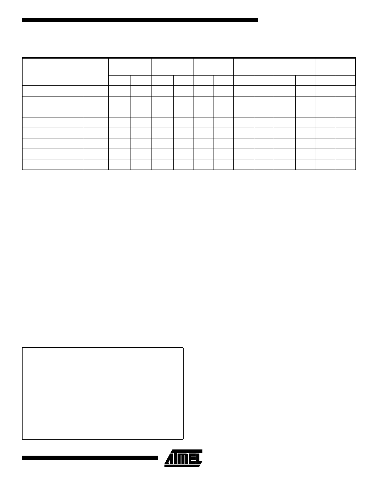
Command Definition (in Hex)
1st Bus
Command
Sequence
Read 1 Addr D
Chip Erase 6 5555 AA 2AAA 55 5555 80 5555 AA 2AAA 55 5555 10
Sector Erase 6 5555 AA 2AAA 55 5555 80 5555 AA 2AAA 55 SA
Byte Program 4 5555 AA 2AAA 55 5555 A0 Addr D
Boot Block Lockout
Product ID Entry 3 5555 AA 2AAA 55 5555 90
Product ID Exit
Product ID Exit
Notes: 1. The DATA FORMAT in each bus cycle is as follows: I/O7 - I/O0 (Hex)
(3)
(3)
2. The 16K byte boot sector has the address range 00000H to 03FFFH for the AT49F002(N) and 3C000H to 3FFFFH for the
AT49F002(N)T
3. Either one of the Product ID Exit commands can be used.
4. SA = sector addresses:
For the AT49F002(N):
SA = 00000 to 03FFF for BOOT BLOCK
Nothing will happen and the device goes back to the read mode in 100 ns
SA = 04000 to 05FFF for PARAMETER BLOCK 1
SA = 06000 to 07FFF for PARAMETER BLOCK 2
SA = 08000 to 1FFFF for MAIN MEMORY ARRAY BLOCK 1
This command will erase - PB1, PB2 and MMB1
SA = 20000 to 3FFFF for MAIN MEMORY ARRAY BLOCK 2
Bus
Cycles
(2)
6 5555 AA 2AAA 55 5555 80 5555 AA 2AAA 55 5555 40
3 5555 AA 2AAA 55 5555 F0
1 XXXX F0
Addr Data Addr Data Addr Data Addr Data Addr Data Addr Data
30
For the AT49F002(N)T:
SA = 3C000 to 3FFFF for BOOT BLOCK
Nothing will happen and the device goes back to the read mode in 100 ns
SA = 3A000 to 3BFFF for PARAMETER BLOCK 1
SA = 38000 to 39FFF for PARAMETER BLOCK 2
SA = 20000 to 37FFF for MAIN MEMORY ARRAY BLOCK 1
This command will erase - PB1, PB2 and MMB1
SA = 00000 to IFFFF for MAIN MEMORY ARRAY BLOCK 2
Absolute Maximum Ratings*
Temperature Under Bias................................ -55°C to +125°C
Storage Temperature.....................................-65°C to +150°C
All Input Voltages
(including NC Pins)
with Respect to Ground...................................-0.6V to +6.25V
All Output Voltages
with Respect to Ground.............................-0.6V to V
Voltage on OE
with Respect to Ground...................................-0.6V to +13.5V
+ 0.6V
CC
*NOTICE: Stresses beyo nd thos e lis ted under “Absolute Maxi-
mum Ratings” may cause permanent damage to the
device. This is a stress rating only and functional
operation of the device at these or any other conditions beyond those indicated in the operational sections of this specification is not implied. Exposure to
absolute maximum rating cond itions for extended
periods may affect device reliability.
5
Page 6
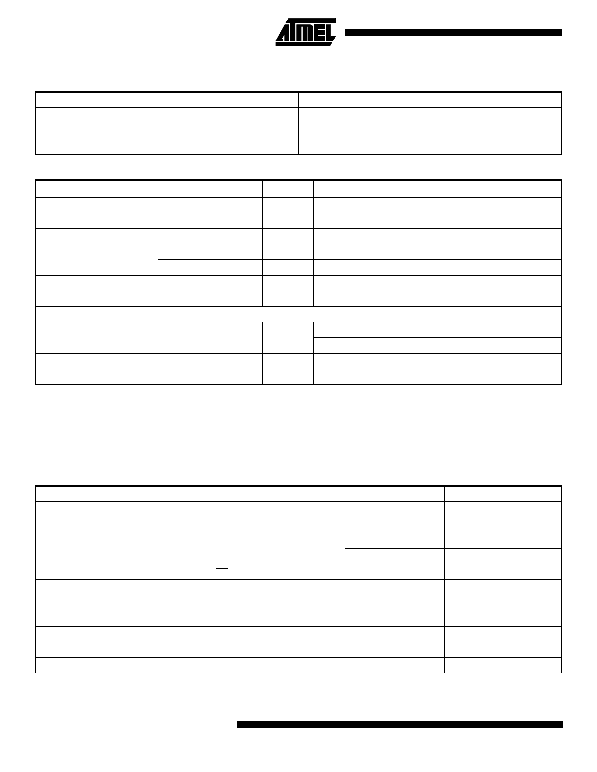
DC and AC Operating Range
AT49F002(N)(T)-55 AT49F002(N)(T)-70 AT49F002(N)(T)-90 AT49F002(N)(T)-12
Operating
Temperature (Case)
Power Supply 5V ± 10% 5V ± 10% 5V ± 10% 5V ± 10%
V
CC
Com. 0
Ind. -40
°C - 70°C0°C - 70°C0°C - 70°C0°C - 70°C
°C - 85°C-40°C - 85°C-40°C - 85°C-40°C - 85°C
Operating Modes
Mode CE OE WE RESET
Read V
Program/Erase
(2)
Standby/Write Inhibit V
IL
V
IL
IH
XXV
Program Inhibit
XVILXV
Output Disable X V
V
IL
V
IH
(1)
X
IH
V
IH
V
IL
XV
IH
XV
Reset XXX V
(6)
V
IH
V
IH
IH
V
IH
IH
IH
IL
Product Identification
Hardware V
Software
(5)
Notes: 1. X can be VIL or V
IH.
IL
V
IL
V
IH
2. Refer to AC Programming Waveforms.
= 12.0V ± 0.5V.
3. V
H
4. Manufacturer Code: 1FH, Device Code: 07H - AT49F002(N), 08H - AT49F002(N)T
5. See details under Software Product Identification Entry/Exit.
6. This pin is not ava ila ble on the AT49F002N(T).
A1 - A17 = VIL, A9 = VH,
A1 - A17 = VIL, A9 = V
A0 = VIL, A1 - A17=V
A0 = VIH, A1 - A17=V
Ai
Ai D
Ai D
I/O
OUT
IN
X High Z
High Z
X High Z
(3)
H,
A0 = V
(3)
A0 = V
IL
IL
Manufacturer Code
IL
Device Code
IH
Manufacturer Code
Device Code
(4)
(4)
(4)
(4)
DC Characteristics
Symbol Parameter Condition Min Max Units
I
I
I
I
I
V
V
V
V
V
LI
LO
SB1
SB2
CC
(1)
IL
IH
OL
OH1
OH2
Input Load Current VIN = 0V to V
Output Leakage Current V
VCC Standby Current CMOS CE = V
VCC Standby Current TTL CE = 2.0V to V
V
Active Current f = 5 MHz; I
CC
Input Low V oltage 0.8 V
Input High Voltage 2.0 V
Output Low Voltage IOL = 2.1 mA 0.45 V
Output High Voltage IOH = -400 µA 2.4 V
Output High Voltage CMOS IOH = -100 µA; VCC = 4.5V 4.2 V
Note: 1. In the erase mode, ICC is 90 mA.
6
AT49F002(N)(T)
= 0V to V
I/O
CC
CC
- 0.3V to V
CC
OUT
CC
CC
= 0 mA 50 mA
Com. 100 µA
Ind. 300 µA
10 µA
10 µA
3mA
Page 7

AC Read Characteristics
AT49F002(N)(T)
AT49F002(N)(T)
-55-70-90-12
Symbol Parameter
t
ACC
t
CE
t
OE
t
DF
(1)
(2)
(3)(4)
Address to Output Delay 55 70 90 120 ns
CE to Output Delay 55 70 90 120 ns
OE to Output Delay 0 30 0 35 0 40 0 50 ns
CE or OE to Output Float 0 25 0 25 0 25 0 30 ns
Output Hold from OE, CE
t
OH
or Address, whichever
occurred first
AC Read Waveforms
Min Max Min Max Min Max Min Max
(1)(2)(3)(4)
ADDRESS
OUTPUT
Units
0000ns
ADDRESS VALID
CE
t
CE
t
t
ACC
HIGH Z
OE
t
DF
t
OH
OUTPUT
VALID
OE
Notes: 1. CE may be delayed up to t
2. OE may be delayed up to tCE - t
without impact on t
is specified from OE or CE whichever occurs first (CL = 5 pF).
3. t
DF
ACC
.
- tCE after the address transition without impact on t
ACC
after the falling edge of CE without impact on tCE or by t
OE
ACC
.
- tOE after an address change
ACC
4. This parameter is characterized and is not 100% tested.
Input Test Waveform and Measurement Level
tR, tF < 5 ns
Output Load Test
50 ns
5.0V
1.8K
OUTPUT
PIN
1.3K
30 pF
70/90/120 ns
5.0V
1.8K
OUTPUT
PIN
1.3K
100 pF
Pin Capacitance
f = 1 MHz, T = 25°C
Symbol Typ Max Units Conditions
C
IN
C
OUT
Note: 1. This parameter is characterized and is not 100% tested.
(1)
46pFV
812pFV
IN
OUT
= 0V
= 0V
7
Page 8

AC Byte Load Characteristics
Symbol Parameter Min Max Units
t
, t
AS
t
AH
t
CS
t
CH
t
WP
t
DS
tDH, t
t
WPH
OES
OEH
Address, OE Set-up Time 0 ns
Address Hold Time 50 ns
Chip Select Set-up Time 0 ns
Chip Select Hold Time 0 ns
Write Pulse Width (WE or CE)90ns
Data Set-up Time 50 ns
Data, OE Hold Time 0 ns
Write Pulse Width High 90 ns
AC Byte Load Waveforms
WE Controlled
CE Controlled
OE
ADDRESS
CE
WE
DATA IN
OE
ADDRESS
WE
t
OES
t
t
t
OES
t
AS
CS
AS
t
OEH
t
AH
t
WP
t
DS
t
AH
t
t
OEH
t
CH
CH
t
t
DH
WPH
t
CS
CE
t
WPH
t
WP
t
DS
t
DH
DATA IN
8
AT49F002(N)(T)
Page 9

AT49F002(N)(T)
Program Cycle Characteristics
Symbol Parameter Min Typ Max Units
t
BP
t
AS
t
AH
t
DS
t
DH
t
WP
t
WPH
t
EC
Program Cyc le Waveforms
Byte Programming Time 10 50 µs
Address Set-up Time 0 ns
Address Hold Time 50 ns
Data Set-up Time 50 ns
Data Hold Time 0 ns
Write Pulse Width 90 ns
Write Pulse Width High 90 ns
Erase Cycle Time 10 seconds
Sector or Chip Erase Cycle Waveforms
Notes: 1. OE must be high only when WE and CE are both low.
2. For chip erase, the address should be 5555. For sector erase, the address depends on what sector is to be erased.
(See note 4 under command definitions.)
3. For chip erase, the data should be 10H, and for sector erase, the data should be 30H.
9
Page 10

Data Poll ing Char acteristics
(1)
Symbol Parameter Min Typ Max Units
t
DH
t
OEH
t
OE
t
WR
Data Hold Time 10 ns
OE Hold Time 10 ns
OE to Output Delay
(2)
Write Recovery Time 0 ns
Notes: 1. These parameters are characterized and not 100% tested.
2. See t
spec in AC Read Characteristics.
OE
Data Polling Waveforms
WE
CE
t
OE
I/O7
t
DH
OEH
t
t
OE
HIGH Z
WR
ns
A0-A17
Toggle Bit Characteristics
(1)
An An An An An
Symbol Parameter Min Typ Max Units
t
DH
t
OEH
t
OE
t
OEHP
t
WR
Data Hold Time 10 ns
OE Hold Time 10 ns
OE to Output Delay
(2)
OE High Pulse 150 ns
Write Recovery Time 0 ns
Notes: 1. These parameters are characterized and not 100% tested.
2. See tOE spec in AC Read Characteristics.
Toggle Bit Wa veforms
WE
CE
OE
I/O6
Notes: 1. Toggling either OE or CE or both OE and CE will operate toggle bit. The t
(1)(2)(3)
t
OEH
t
OE
t
DH
t
OEHP
HIGH Z
t
WR
specification must be met by the toggling
OEHP
input(s).
2. Beginning and ending state of I/O6 will vary.
3. Any address location may be used but the address should not vary.
ns
10
AT49F002(N)(T)
Page 11

AT49F002(N)(T)
LOAD DATA AA
TO
ADDRESS 5555
LOAD DATA 55
TO
ADDRESS 2AAA
LOAD DATA 90
TO
ADDRESS 5555
ENTER PRODUCT
IDENTIFICATION
MODE
(2)(3)(5)
LOAD DATA AA
TO
ADDRESS 5555
LOAD DATA 55
TO
ADDRESS 2AAA
LOAD DATA F0
TO
ADDRESS 5555
EXIT PRODUCT
IDENTIFICATION
MODE
(4)
OR
LOAD DATA F0
TO
ANY ADDRESS
EXIT PRODUCT
IDENTIFICATION
MODE
(4)
Software Product Identification Entry
Software Product Identification Exit
Notes for software product identification
1. Data Format: I/O7 - I/O0 (Hex);
Address Format: A14 - A0 (Hex).
2. A1 - A17 = V
Manufacture Code is read for A0 = V
Device Code is read for A0 = V
3. The device does not remain in identification mode if
powered down.
4. The device returns to standard operation mode.
5. Manufacturer Code: 1FH
Device Code: 07H - AT49F002(N)
.
IL
08H - AT49F002(N)T
;
IL
.
IH
(1)
(1)
Boot Block Lockout Feature Enabl e
Algorithm
Notes for boot block lockout feature enable:
1. Data Format: I/O7 - I/O0 (Hex);
Address Format: A14 - A0 (Hex).
2. Boot block lockout feature enabled.
(1)
LOAD DATA AA
TO
ADDRESS 5555
LOAD DATA 55
TO
ADDRESS 2AAA
LOAD DATA 80
TO
ADDRESS 5555
LOAD DATA AA
TO
ADDRESS 5555
LOAD DATA 55
TO
ADDRESS 2AAA
LOAD DATA 40
TO
ADDRESS 5555
PAUSE 1 second
(2)
11
Page 12

AT49F002 Ordering Information
I
(mA)
t
ACC
(ns)
55 50 0.1 AT49F002-55JC
70 50 0.1 AT49F002-70JC
90 50 0.1 AT49F002-90JC
120 50 0.1 AT49F002-12JC
CC
Ordering Code Package Operation RangeActive Standby
AT49F002-55PC
AT49F002-55TC
AT49F002-55VC
50 0.3 AT49F002-55JI
AT49F002-55PI
AT49F002-55TI
AT49F002-55VI
AT49F002-70PC
AT49F002-70TC
AT49F002-70VC
50 0.3 AT49F002-70JI
AT49F002-70PI
AT49F002-70TI
AT49F002-70VI
AT49F002-90PC
AT49F002-90TC
AT49F002-90VC
50 0.3 AT49F002-90JI
AT49F002-90PI
AT49F002-90TI
AT49F002-90VI
AT49F002-12PC
AT49F002-12TC
AT49F002-12VC
50 0.3 AT49F002-12JI
AT49F002-12PI
AT49F002-12TI
AT49F002-12VI
32J
32P6
32T
32V
32J
32P6
32T
32V
32J
32P6
32T
32V
32J
32P6
32T
32V
32J
32P6
32T
32V
32J
32P6
32T
32V
32J
32P6
32T
32V
32J
32P6
32T
32V
Commercial
(0° to 70°C)
Industrial
(-40° to 85°C)
Commercial
(0° to 70°C)
Industrial
(-40° to 85°C)
Commercial
(0° to 70°C)
Industrial
(-40° to 85°C)
Commercial
(0° to 70°C)
Industrial
(-40° to 85°C)
Package Type
32J 32-lead, Plastic J-leaded Chip Carrier Package (PLCC)
32P6 32-pin, 0.600" Wide, Plastic Dual Inline Package (PDIP)
32T 32-lead, Plastic Thin Small Outline Package (TSOP) (8 x 20 mm)
32V 32-lead, Plastic Thin Small Outline Package (VSOP) (8 x 14 mm)
12
AT49F002(N)(T)
Page 13

AT49F002N Ordering Information
I
(mA)
t
ACC
(ns)
55 50 0.1 AT49F002N-55JC
70 50 0.1 AT49F002N-70JC
90 50 0.1 AT49F002N-90JC
120 50 0.1 AT49F002N-12JC
CC
Ordering Code Package Operation RangeActive Standby
AT49F002N-55PC
AT49F002N-55TC
AT49F002N-55VC
50 0.3 AT49F002N-55JI
AT49F002N-55PI
AT49F002N-55TI
AT49F002N-55VI
AT49F002N-70PC
AT49F002N-70TC
AT49F002N-70VC
50 0.3 AT49F002N-70JI
AT49F002N-70PI
AT49F002N-70TI
AT49F002N-70VI
AT49F002N-90PC
AT49F002N-90TC
AT49F002N-90VC
50 0.3 AT49F002N-90JI
AT49F002N-90PI
AT49F002N-90TI
AT49F002N-90VI
AT49F002N-12PC
AT49F002N-12TC
AT49F002N-12VC
50 0.3 AT49F002N-12JI
AT49F002N-12PI
AT49F002N-12TI
AT49F002N-12VI
32J
32P6
32T
32V
32J
32P6
32T
32V
32J
32P6
32T
32V
32J
32P6
32T
32V
32J
32P6
32T
32V
32J
32P6
32T
32V
32J
32P6
32T
32V
32J
32P6
32T
32V
AT49F002(N)(T)
Commercial
(0° to 70°C)
Industrial
(-40° to 85°C)
Commercial
(0° to 70°C)
Industrial
(-40° to 85°C)
Commercial
(0° to 70°C)
Industrial
(-40° to 85°C)
Commercial
(0° to 70°C)
Industrial
(-40° to 85°C)
Package Type
32J 32-lead, Plastic J-leaded Chip Carrier Package (PLCC)
32P6 32-pin, 0.600" Wide, Plastic Dual Inline Package (PDIP)
32T 32-lead, Plastic Thin Small Outline Package (TSOP) (8 x 20 mm)
32V 32-lead, Plastic Thin Small Outline Package (VSOP) (8 x 14 mm)
13
Page 14

AT49F002T Ordering Information
I
(mA)
t
ACC
(ns)
55 50 0.1 AT49F002T-55JC
70 50 0.1 AT49F002T-70JC
90 50 0.1 AT49F002T-90JC
120 50 0.1 AT49F002T-12JC
CC
Ordering Code Package Operation RangeActive Standby
AT49F002T-55PC
AT49F002T-55TC
AT49F002T-55VC
50 0.3 AT49F002T-55JI
AT49F002T-55PI
AT49F002T-55TI
AT49F002T-55VI
AT49F002T-70PC
AT49F002T-70TC
AT49F002T-70VC
50 0.3 AT49F002T-70JI
AT49F002T-70PI
AT49F002T-70TI
AT49F002T-70VI
AT49F002T-90PC
AT49F002T-90TC
AT49F002T-90VC
50 0.3 AT49F002T-90JI
AT49F002T-90PI
AT49F002T-90TI
AT49F002T-90VI
AT49F002T-12PC
AT49F002T-12TC
AT49F002T-12VC
50 0.3 AT49F002T-12JI
AT49F002T-12PI
AT49F002T-12TI
AT49F002T-12VI
32J
32P6
32T
32V
32J
32P6
32T
32V
32J
32P6
32T
32V
32J
32P6
32T
32V
32J
32P6
32T
32V
32J
32P6
32T
32V
32J
32P6
32T
32V
32J
32P6
32T
32V
Commercial
(0° to 70°C)
Industrial
(-40° to 85°C)
Commercial
(0° to 70°C)
Industrial
(-40° to 85°C)
Commercial
(0° to 70°C)
Industrial
(-40° to 85°C)
Commercial
(0° to 70°C)
Industrial
(-40° to 85°C)
Package Type
32J 32-lead, Plastic J-leaded Chip Carrier Package (PLCC)
32P6 32-pin, 0.600" Wide, Plastic Dual Inline Package (PDIP)
32T 32-lead, Plastic Thin Small Outline Package (TSOP) (8 x 20 mm)
32V 32-lead, Plastic Thin Small Outline Package (VSOP) (8 x 14 mm)
14
AT49F002(N)(T)
Page 15

AT49F002NT Ordering Information
I
(mA)
t
ACC
(ns)
55 50 0.1 AT49F002NT-55JC
70 50 0.1 AT49F002NT-70JC
90 50 0.1 AT49F002NT-90JC
120 50 0.1 AT49F002NT-12JC
CC
Ordering Code Package Operation RangeActive Standby
AT49F002NT-55PC
AT49F002NT-55TC
AT49F002NT-55VC
50 0.3 AT49F002NT-55JI
AT49F002NT-55PI
AT49F002NT-55TI
AT49F002NT-55VI
AT49F002NT-70PC
AT49F002NT-70TC
AT49F002NT-70VC
50 0.3 AT49F002NT-70JI
AT49F002NT-70PI
AT49F002NT-70TI
AT49F002NT-70VI
AT49F002NT-90PC
AT49F002NT-90TC
AT49F002NT-90VC
50 0.3 AT49F002NT-90JI
AT49F002NT-90PI
AT49F002NT-90TI
AT49F002NT-90VI
AT49F002NT-12PC
AT49F002NT-12TC
AT49F002NT-12VC
50 0.3 AT49F002NT-12JI
AT49F002NT-12PI
AT49F002NT-12TI
AT49F002NT-12VI
32J
32P6
32T
32V
32J
32P6
32T
32V
32J
32P6
32T
32V
32J
32P6
32T
32V
32J
32P6
32T
32V
32J
32P6
32T
32V
32J
32P6
32T
32V
32J
32P6
32T
32V
AT49F002(N)(T)
Commercial
(0° to 70°C)
Industrial
(-40° to 85°C)
Commercial
(0° to 70°C)
Industrial
(-40° to 85°C)
Commercial
(0° to 70°C)
Industrial
(-40° to 85°C)
Commercial
(0° to 70°C)
Industrial
(-40° to 85°C)
Package Type
32J 32-lead, Plastic J-leaded Chip Carrier Package (PLCC)
32P6 32-pin, 0.600" Wide, Plastic Dual Inline Package (PDIP)
32T 32-lead, Plastic Thin Small Outline Package (TSOP) (8 x 20 mm)
32V 32-lead, Plastic Thin Small Outline Package (VSOP) (8 x 14 mm)
15
Page 16

Pac ka ging Inf ormation
32J, 32-lead, Plastic J-leaded Chip Carrier (PLC C)
Dimensions in Inches and (Millimeters)
JEDEC STANDARD MS-016 AE
.045(1.14) X 45˚
.032(.813)
.026(.660)
.050(1.27) TYP
PIN NO.1
IDENTIFY
.553(14.0)
.547(13.9)
.300(7.62) REF
.430(10.9)
.390(9.90)
.453(11.5)
.447(11.4)
.495(12.6)
.485(12.3)
.025(.635) X 30˚ - 45˚
.595(15.1)
.585(14.9)
AT CONTACT
POINTS
.022(.559) X 45˚ MAX (3X)
.012(.305)
.008(.203)
.530(13.5)
.490(12.4)
.021(.533)
.013(.330)
.030(.762)
.015(.381)
.095(2.41)
.060(1.52)
.140(3.56)
.120(3.05)
32P6, 32-pin, 0.600" Wide,
Plastic Dual Inline Package (PDIP)
Dimensions in Inches and (Millimeters)
1.67(42.4)
.220(5.59)
SEATING
PLANE
MAX
.161(4.09)
.125(3.18)
.110(2.79)
.090(2.29)
.012(.305)
.008(.203)
1.64(41.7)
1.500(38.10) REF
.065(1.65)
.041(1.04)
.630(16.0)
.590(15.0)
.690(17.5)
.610(15.5)
PIN
0
REF
15
1
.566(14.4)
.530(13.5)
.090(2.29)
.005(.127)
.065(1.65)
.015(.381)
.022(.559)
.014(.356)
MAX
MIN
32T, 32-lead, Plastic Thin Small Outline Package
(TSOP)
Dimensions in Millimeters and (Inches)*
INDEX
MARK
0.50(.020)
BSC
0
REF
5
7.50(.295)
REF
8.20(.323)
7.80(.307)
0.15(.006)
0.05(.002)
18.5(.728)
18.3(.720)
0.25(.010)
0.15(.006)
0.70(.028)
0.50(.020)
20.2(.795)
19.8(.780)
1.20(.047) MAX
0.20(.008)
0.10(.004)
*Controlling dimension: millimeters
32V, 32-lead, Plastic Thin Small Outline Package
(TSOP)
Dimensions in Millimeters and (Inches)
INDEX
MARK
0.50(.020)
BSC
0
REF
5
7.50(.295)
REF
8.10(.319)
7.90(.311)
0.15(.006)
0.05(.002)
12.5(.492)
12.3(.484)
0.25(.010)
0.15(.006)
0.70(.028)
0.50(.020)
14.2(.559)
13.8(.543)
1.20(.047) MAX
0.20(.008)
0.10(.004)
16
AT49F002(N)(T)
Page 17

Atmel Headquarters Atmel Operations
Corporate Headquarters
2325 Orchard Parkway
San Jose, CA 95131
TEL (408) 441- 0311
FAX (408) 487-2600
Europe
Atmel U.K., Ltd.
Coliseum Business Centre
Riverside Way
Camberley, Surrey GU15 3YL
England
TEL (44) 1276-686-677
FAX (44) 1276-686-697
Asia
Atmel Asia, Ltd.
Room 1219
Chinachem Golden Plaza
77 Mody Road Tsimhatsui
East Kowloon
Hong Kong
TEL (852) 2721- 9778
FAX (852) 2722-1369
Japan
Atmel Japan K.K.
9F, Tonetsu Shinkawa Bldg.
1-24-8 Shinka wa
Chuo-ku, Tokyo 104-0033
Japan
TEL (81) 3-3523-3551
FAX (81) 3-3523-7581
Atmel Colorado Springs
1150 E. Cheyenne Mtn. Blvd.
Colorado Springs, CO 80906
TEL (719) 576-3300
FAX (719) 540-1759
Atmel Rousset
Zone Indus triel le
13106 Rousset Cedex
France
TEL (33) 4-4253-6000
FAX (33) 4-4253-6001
Fax-on-Demand
North America:
1-(800) 292-8635
International:
1-(408) 441-0732
e-mail
literature@atmel.com
Web Site
http://www.atmel.com
BBS
1-(408) 436-4309
© Atmel Corporation 1999.
Atmel Corporation makes no warranty for the use of its products, other than those expressly contained in the Company’s standard warranty which is detailed in Atmel’s Terms and Conditions located on the Company’s web site. The Company assumes no responsibility for
any errors which may appear in this document, reserves the right to change devices or specifications detailed herein at any time without
notice, and does not make any commitment to update the information contained herein. No licenses to patents or other intellectual property of Atmel are granted by the Company in connection with the sale of Atmel products, expressly or by implication. Atmel’s products are
not authorized for use as critical components in life support devices or systems.
®
Marks b eari ng
Ter ms and product names in this document may be trademarks of others.
and/or ™ are registered trademarks and trademarks of Atmel Corporation.
Printed on recycled paper.
1017D–10/99/xM
 Loading...