

Page 1

AT45DQ321
32-Mbit DataFlash (with Extra 1-Mbits), 2.3V or 2.5V Minimum
SPI Serial Flash Memory with Dual-I/O and Quad-I/O Support
ADVANCE DATASHEET
Features
Single 2.3V - 3.6V or 2.5V - 3.6V supply
Serial Peripheral Interface (SPI) compatible
Supports SPI modes 0 and 3
Supports RapidS
Supports Dual-input and Quad-input Buffer Write
Supports Dual-output and Quad-output Read
Very high operating frequencies
85MHz (for SPI)
85MHz (for Dual-I/O and Quad-I/O)
Clock-to-output time (t
User configurable page size
512 bytes per page
528 bytes per page (default)
Page size can be factory pre-configured for 512 bytes
Two fully independent SRAM data buffers (512/528 bytes)
Allows receiving data while reprogramming the main memory array
Flexible programming options
Byte/Page Program (1 to 512/528 bytes) directly into main memory
Buffer Write
Buffer to Main Memory Page Program
Flexible erase options
Page Erase (512/528 bytes)
Block Erase (4KB)
Sector Erase (64KB)
Chip Erase (32-Mbits)
Program and Erase Suspend/Resume
Advanced hardware and software data protection features
Individual sector protection
Individual sector lockdown to make any sector permanently read-only
128-byte, One-Time Programmable (OTP) Security Register
64 bytes factory programmed with a unique identifier
64 bytes user programmable
Hardware and software controlled reset options
JEDEC Standard Manufacturer and Device ID Read
Low-power dissipation
500nA Ultra-Deep Power-Down current (typical)
3μA Deep Power-Down current (typical)
25μA Standby current (typical)
11mA Active Read current (typical at 20MHz)
Endurance: 100,000 program/erase cycles per page minimum
Data retention: 20 years
Complies with full industrial temperature range
Green (Pb/Halide-free/RoHS compliant) packaging options
8-lead SOIC (0.208" wide)
8-pad Ultra-thin DFN (5 x 6 x 0.6mm)
9-ball Ultra-thin UBGA (6 x 6 x 0.6mm)
™
operation
) of 6ns maximum
V
DS-45DQ321-031–DFLASH–12/2012
Page 2
Description
The AT45DQ321 is a 2.3V or 2.5V minimum, serial-interface sequential access Flash memory ideally suited for a wide
variety of digital voice, image, program code, and data storage applications. The AT45DQ321 also supports Dual-I/O,
Quad-I/O and the RapidS serial interface for applications requiring very high speed operation. Its 34,603,008 bits of
memory are organized as 8,192 pages of 512 bytes or 528 bytes each. In addition to the main memory, the AT45DQ321
also contains two SRAM buffers of 512/528 bytes each. The buffers allow receiving of data while a page in the main
memory is being reprogrammed. Interleaving between both buffers can dramatically increase a system's ability to write a
continuous data stream. In addition, the SRAM buffers can be used as additional system scratch pad memory, and
2
PROM emulation (bit or byte alterability) can be easily handled with a self-contained three step read-modify-write
E
operation.
Unlike conventional Flash memories that are accessed randomly with multiple address lines and a parallel interface, the
DataFlash
active pin count, facilitates simplified hardware layout, increases system reliability, minimizes switching noise, and
reduces package size. The device is optimized for use in many commercial and industrial applications where highdensity, low-pin count, low-voltage, and low-power are essential.
To allow for simple in-system re-programmability, the AT45DQ321 does not require high input voltages for programming.
The device operates from a single 2.3V to 3.6V or 2.5V to 3.6V power supply for the erase and program and read
operations. The AT45DQ321 is enabled through the Chip Select pin (
of the Serial Input (SI), Serial Output (SO), and the Serial Clock (SCK).
All programming and erase cycles are self-timed.
®
uses a serial interface to sequentially access its data. The simple sequential access dramatically reduces
CS) and accessed via a 3-wire interface consisting
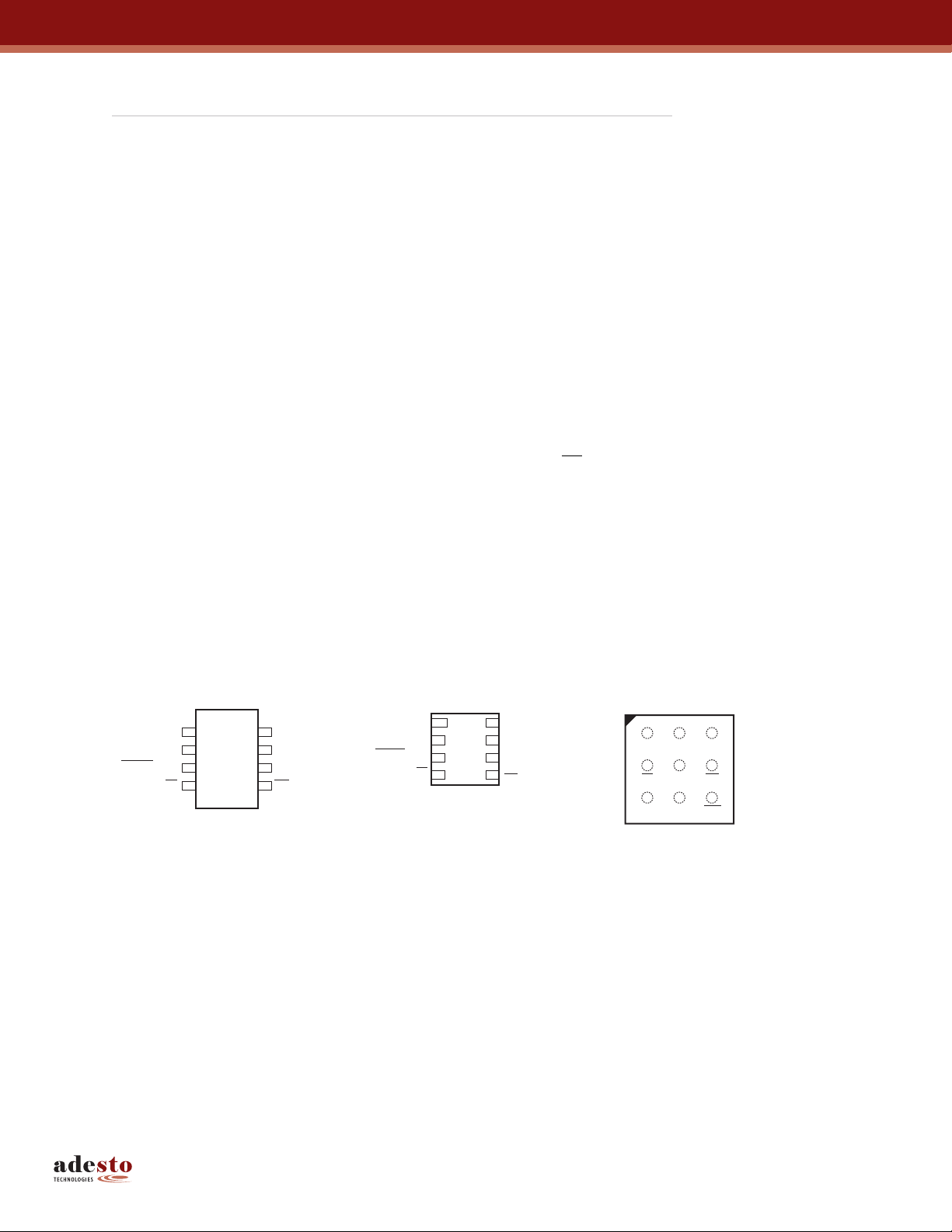
1. Pin Configurations and Pinouts
Figure 1-1. Pinouts
8-lead SOIC
Top View
SI (I/O0)
SCK
RESET (I/O
3
CS
SCK
CS
1
2
3
4
8
7
6
5
SO (I/O1)
GND
V
CC
WP (I/O2)
SI (I/O0)
RESET (I/O3)
Note: 1. The metal pad on the bottom of the UDFN package is not internally connected to a voltage potential.
This pad can be a “no connect” or connected to GND.
8-pad UDFN
Top View
1
2
3
)
4
8
7
6
5
SO
GND
V
CC
WP
(I/O
(I/O
9-ball UBGA
Top View
1
)
SCK GND V
2
)
SO SI RST
CC
WPNCCS
AT45DQ321 [ADVANCE DATASHEET]
DS-45DQ321-031–DFLASH–12/2012
2
Page 3

Table 1-1. Pin Configurations
Symbol Name and Function
Chip Select: Asserting the CS pin selects the device. When the CS pin is deasserted, the
device will be deselected and normally be placed in the standby mode (not Deep Power-Down
mode) and the output pin (SO) will be in a high-impedance state. When the device is
CS
deselected, data will not be accepted on the input pin (SI).
A high-to-low transition on the
transition is required to end an operation. When ending an internally self-timed operation such
as a program or erase cycle, the device will not enter the standby mode until the completion of
the operation.
Serial Clock: This pin is used to provide a clock to the device and is used to control the flow of
SCK
data to and from the device. Command, address, and input data present on the SI pin is
always latched on the rising edge of SCK, while output data on the SO pin is always clocked
out on the falling edge of SCK.
Serial Input (I/O0): The SI pin is used to shift data into the device. The SI pin is used for all
data input including command and address sequences. Data on the SI pin is always latched on
the rising edge of SCK.
With the Dual-output and Quad-output Read Array commands, the SI pin becomes an output
SI (I/O0)
pin (I/O
be clocked out on every falling edge of SCK. To maintain consistency with SPI nomenclature,
the SI (I/O
) and, along with other pins, allows two bits (on I/O
0
) pin will be referenced as SI throughout the document with exception to sections
0
dealing with the Dual-output and Quad-output Read Array commands in which it will be
referenced as I/O
Data present on the SI pin will be ignored whenever the device is deselected (
deasserted).
Asserted
CS pin is required to start an operation and a low-to-high
State
Low Input
Type
— Input
) or four bits (on I/O
1-0
.
0
) of data to
3-0
—
Input/
Output
CS is
SO (I/O1)
Serial Output (I/O1): The SO pin is used to shift data out from the device. Data on the SO pin
is always clocked out on the falling edge of SCK.
With the Dual-output and Quad-output Read Array commands, the SO pin is used as an output
pin (I/O
) in conjunction with other pins to allow two bits (on I/O
1
) or four bits (on I/O
1-0
) of data
3-0
to be clocked out on every falling edge of SCK. To maintain consistency with SPI
nomenclature, the SO (I/O
) pin will be referenced as SO throughout the document with
1
exception to sections dealing with the Dual-output and Quad-output Read Array commands in
which it will be referenced as I/O
The SO pin will be in a high-impedance state whenever the device is deselected (
.
1
CS is
deasserted).
—
Input/
Output
AT45DQ321 [ADVANCE DATASHEET]
DS-45DQ321-031–DFLASH–12/2012
3
Page 4
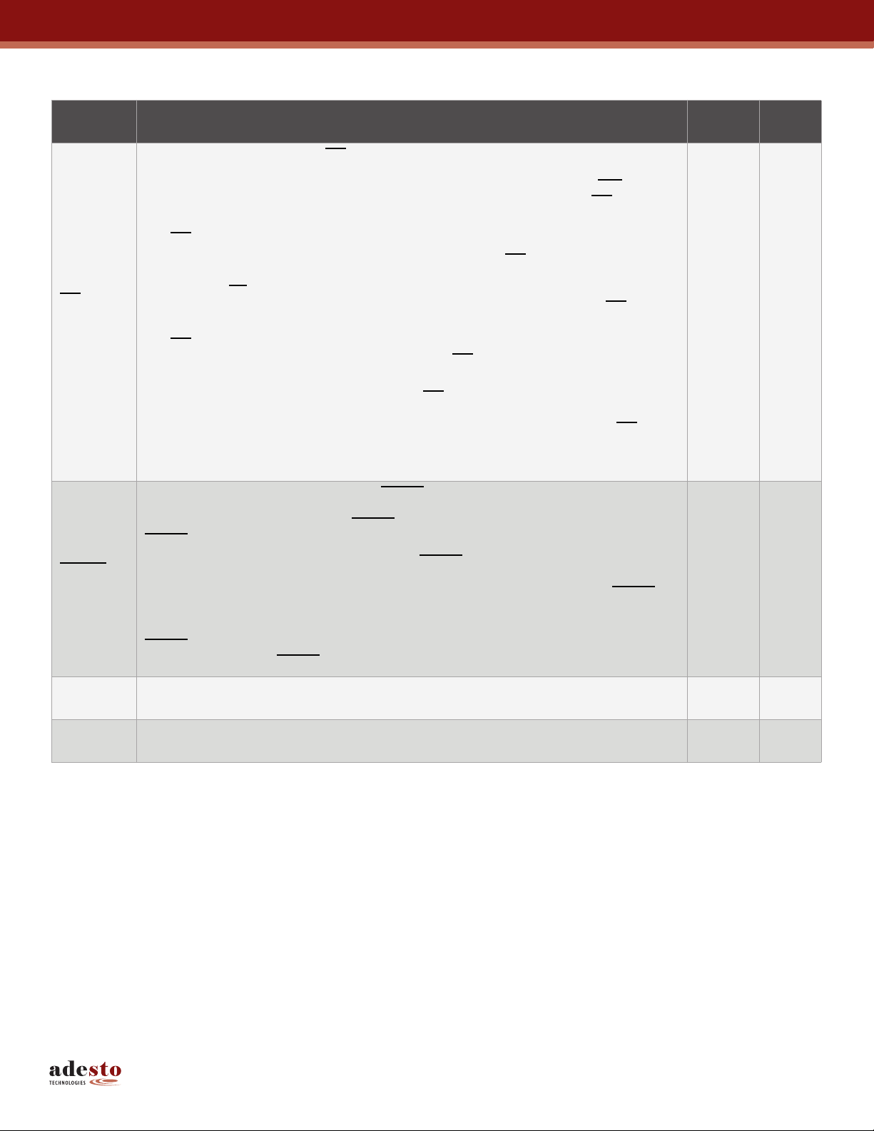
Table 1-1. Pin Configurations (Continued)
Symbol Name and Function
Write Protect (I/O2): When the WP pin is asserted, all sectors specified for protection by the
Sector Protection Register will be protected against program and erase operations regardless
of whether the Enable Sector Protection command has been issued or not. The
functions independently of the software controlled protection method. After the
low, the contents of the Sector Protection Register cannot be modified.
WP pin must be driven at all times or pulled-high using an external pull-up resistor.
The
If a program or erase command is issued to the device while the
will simply ignore the command and perform no operation. The device will return to the idle
WP (I/O2)
state once the
Sector Lockdown command, however, will be recognized by the device when the
CS pin has been deasserted. The Enable Sector Protection command and the
asserted.
WP pin is internally pulled-high and may be left floating if hardware controlled protection
The
will not be used. However, it is recommended that the
V
whenever possible.
CC
With the Quad-output Read Array command, the
when used with other pins, allows four bits (on I/O
edge of SCK. The QE bit in the Configuration Register must be set in order for the
be used as an I/O data pin.
Reset (I/O3): A low state on the reset pin (RESET) will terminate the operation in progress and
reset the internal state machine to an idle state. The device will remain in the reset condition as
long as a low level is present on the
RESET pin is brought back to a high level.
RESET
(I/O
)
3
With the Quad-output Read Array command, the
when used with other pins, allows four bits (on I/O
edge of SCK. The QE bit in the Configuration Register must be set in order for the
to be used as an I/O data pin.
The device incorporates an internal power-on reset circuit, so there are no restrictions on the
RESET pin during power-on sequences. If this pin and feature is not utilized, then it is
recommended that the
RESET pin be driven high externally.
WP pin
WP pin goes
WP pin is asserted, the device
WP pin is
WP pin also be externally connected to
WP pin becomes an output pin (I/O2) and,
) of data to be clocked out on every falling
3-0
WP pin to
RESET pin. Normal operation can resume once the
RESET pin becomes an output pin (I/O3) and,
) of data to be clocked out on every falling
3-0
RESET pin
Asserted
State
Low
Low
Type
Input/
Output
Input/
Output
V
CC
GND
Device Power Supply: The VCC pin is used to supply the source voltage to the device.
Operations at invalid V
voltages may produce spurious results and should not be attempted.
CC
Ground: The ground reference for the power supply. GND should be connected to the system
ground.
AT45DQ321 [ADVANCE DATASHEET]
DS-45DQ321-031–DFLASH–12/2012
— Power
— Ground
4
Page 5
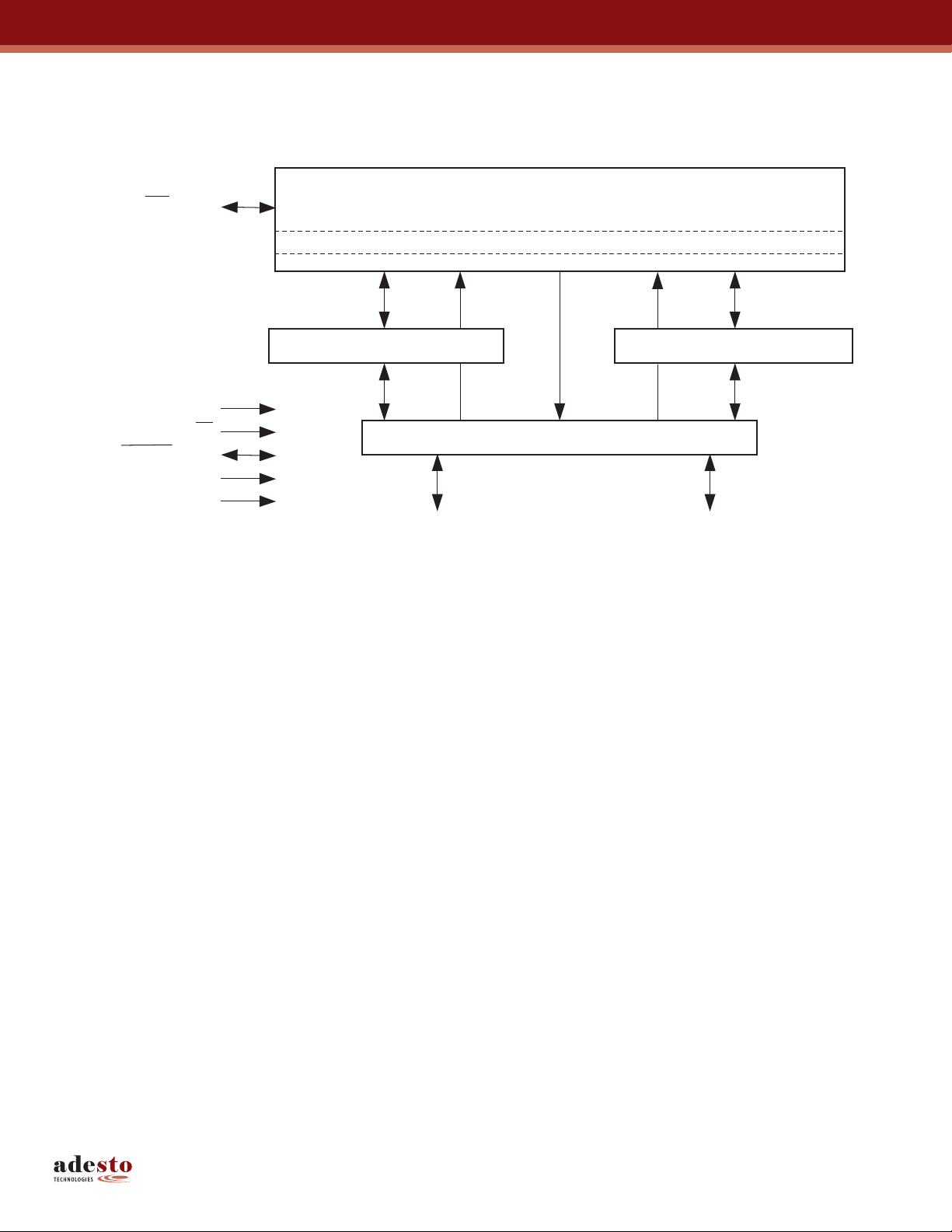
2. Block Diagram
Figure 2-1. Block Diagram
)
(I/O
WP
RESET
SCK
(I/O
V
GND
2
CS
3
CC
)
Flash Memory Array
Page (512/528 bytes)
Buffer 1 (512/528 bytes) Buffer 2 (512/528 bytes)
I/O Interface
(I/O
(I/O0)
SOSI
)
1
Note: I/O
pin naming convention is used for Dual-I/O and Quad-I/O commands.
3-0
AT45DQ321 [ADVANCE DATASHEET]
DS-45DQ321-031–DFLASH–12/2012
5
Page 6
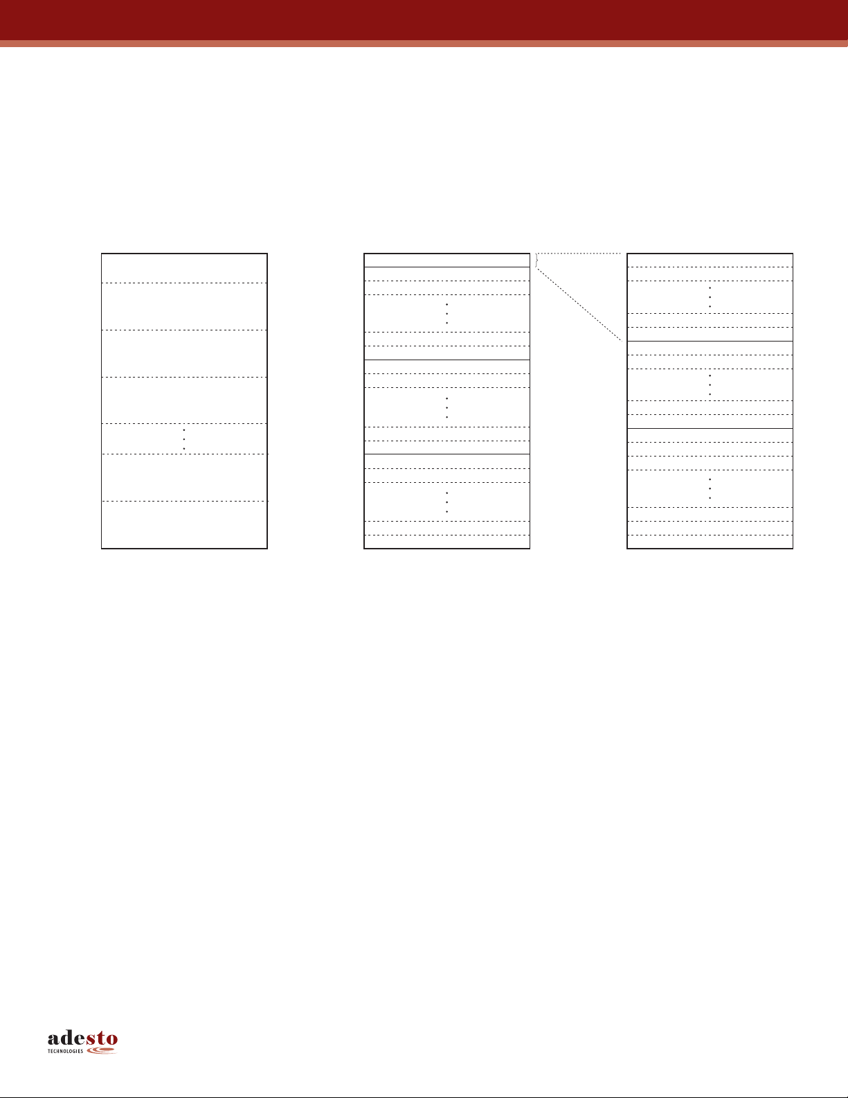
3. Memory Array
To provide optimal flexibility, the AT45DQ321 memory array is divided into three levels of granularity comprising of
sectors, blocks, and pages. Figure 3-1, Memory Architecture Diagram illustrates the breakdown of each level and details
the number of pages per sector and block. Program operations to the DataFlash can be done at the full page level or at
the byte level (a variable number of bytes). The erase operations can be performed at the chip, sector, block, or page
level.
Figure 3-1. Memory Architecture Diagram
Sector Architecture Block Architecture Page Architecture
Sector 0a = 8 pages
4,096/4,224 bytes
Sector 0b = 120 pages
61,440/63,360 bytes
Sector 1 = 128 pages
65,536/67,584 bytes
Sector 2 = 128 pages
65,536/67,584 bytes
Sector 62 = 128 pages
65,536/67,584 bytes
Sector 0a
Sector 0b
Sector 1
Block 0
Block 1
Block 2
Block 30
Block 31
Block 32
Block 33
Block 62
Block 63
Block 64
Block 65
8 Pages
Block 0
Block 1
Page 0
Page 1
Page 6
Page 7
Page 8
Page 9
Page 14
Page 15
Page 16
Page 17
Page 18
Sector 63 = 128 pages
65,536/67,584 bytes
Block 1022
Block 1023
Block = 4,096/4,224 bytes
Page 8,190
Page 8,191
Page = 512/528 bytes
AT45DQ321 [ADVANCE DATASHEET]
DS-45DQ321-031–DFLASH–12/2012
6
Page 7

4. Device Operation
The device operation is controlled by instructions from the host processor. The list of instructions and their associated
opcodes are contained in Table 15-1 on page 47 through Table 15-4 on page 48. A valid instruction starts with the falling
edge of
CS pin is low, toggling the SCK pin controls the loading of the opcode and the desired buffer or main memory address
location through the SI (Serial Input) pin. All instructions, addresses, and data are transferred with the Most Significant Bit
(MSB) first.
Three address bytes are used to address memory locations in either the main memory array or in one of the SRAM
buffers. The three address bytes will be comprised of a number of dummy bits and a number of actual device address
bits, with the number of dummy bits varying depending on the operation being performed and the selected device page
size. Buffer addressing for the standard DataFlash page size (528 bytes) is referenced in the datasheet using the
terminology BFA9 - BFA0 to denote the 10 address bits required to designate a byte address within a buffer. The main
memory addressing is referenced using the terminology PA12 - PA0 and BA9 - BA0, where PA12 - PA0 denotes the
13 address bits required to designate a page address, and BA9 - BA0 denotes the 10 address bits required to designate
a byte address within the page. Therefore, when using the standard DataFlash page size, a total of 23 address bits are
used.
For the “power of 2” binary page size (512 bytes), the buffer addressing is referenced in the datasheet using the
conventional terminology BFA8 - BFA0 to denote the 9 address bits required to designate a byte address within a buffer.
Main memory addressing is referenced using the terminology A21 - A0, where A21 - A9 denotes the 13 address bits
required to designate a page address, and A8 - A0 denotes the 9 address bits required to designate a byte address
within a page. Therefore, when using the binary page size, a total of 22 address bits are used.
CS followed by the appropriate 8-bit opcode and the desired buffer or main memory address location. While the
4.1 Dual-I/O and Quad I/O Operation
The AT45DQ321 features a Dual-input Buffer Write mode and a Dual-output Read mode that allows two bits of data to be
clocked into Buffer 1 or Buffer 2 or allows two bits of data to be read out of the device on every clock cycle to improve
throughputs. To accomplish this, both the SI and SO pins are utilized as inputs/outputs for the transfer of data bytes. With
the Dual-input Buffer Write command, the SO pin becomes an input along with the SI pin. Alternatively, with the Dualoutput Read Array command, the SI pin becomes an output along with the SO pin. For both Dual-I/O commands, the SO
pin will be referrred to as I/O
The device also supports a Quad-input Buffer Write mode and a Quad-output Read mode in which the
pins become data pins for even higher throughputs by allowing four bits of data to be clocked on every clock cycle into
one of the buffers or by allowing four bits of data to be read out of the device on every clock cycle. For the Quad-input
Buffer Write and Quad-output Read Array commands, the
RESET becomes I/O
, WP becomes I/O2, SO becomes I/O1 and SI becomes I/O0. The QE bit in the Configuration
3
Register must be set (via issuing the Quad Enable command) to enable the Quad-I/O operation and to enable the
WP pins to be converted to I/O data pins.
and
and the SI pin will be referred to as I/O0.
1
WP and RESET
RESET, WP, SO and SI pins are referred to as I/O
where
3-0
RESET
AT45DQ321 [ADVANCE DATASHEET]
DS-45DQ321-031–DFLASH–12/2012
7
Page 8

5. Read Commands
By specifying the appropriate opcode, data can be read from the main memory or from either one of the two SRAM data
buffers. The DataFlash supports RapidS protocols for Mode 0 and Mode 3. Please see Section 25., Detailed Bit-level
Read Waveforms: RapidS Mode 0/Mode 3 diagrams in this datasheet for details on the clock cycle sequences for each
mode.
5.1 Continuous Array Read (Legacy Command: E8h Opcode)
By supplying an initial starting address for the main memory array, the Continuous Array Read command can be utilized to
sequentially read a continuous stream of data from the device by simply providing a clock signal; no additional addressing
information or control signals need to be provided. The DataFlash incorporates an internal address counter that will
automatically increment on every clock cycle, allowing one continuous read from memory to be performed without the
need for additional address sequences. To perform a Continuous Array Read using the standard DataFlash page size
(528 bytes), an opcode of E8h must be clocked into the device followed by three address bytes (which comprise the 23-bit
page and byte address sequence) and four dummy bytes. The first 13 bits (PA12 - PA0) of the 23-bit address sequence
specify which page of the main memory array to read and the last 10 bits (BA9 - BA0) of the 23-bit address sequence
specify the starting byte address within the page. To perform a Continuous Array Read using the binary page size
(512 bytes), an opcode of E8h must be clocked into the device followed by three address bytes and four dummy bytes.
The first 13 bits (A21 - A9) of the 22-bit address sequence specify which page of the main memory array to read and the
last 9 bits (A8 - A0) of the 22-bit address sequence specify the starting byte address within the page. The dummy bytes
that follow the address bytes are needed to initialize the read operation. Following the dummy bytes, additional clock
pulses on the SCK pin will result in data being output on the SO (serial output) pin.
CS pin must remain low during the loading of the opcode, the address bytes, the dummy bytes, and the reading of
The
data. When the end of a page in the main memory is reached during a Continuous Array Read, the device will continue
reading at the beginning of the next page with no delays incurred during the page boundary crossover (the crossover from
the end of one page to the beginning of the next page). When the last bit in the main memory array has been read, the
device will continue reading back at the beginning of the first page of memory. As with crossing over page boundaries, no
delays will be incurred when wrapping around from the end of the array to the beginning of the array.
A low-to-high transition on the
SCK frequency allowable for the Continuous Array Read is defined by the f
bypasses the data buffers and leaves the contents of the buffers unchanged.
CS pin will terminate the read operation and tri-state the output pin (SO). The maximum
CAR1
specification. The Continuous Array Read
5.2 Continuous Array Read (High Frequency Mode: 1Bh Opcode)
This command can be used to read the main memory array sequentially at the highest possible operating clock
frequency up to the maximum specified by f
page size (528 bytes), the
CS pin must first be asserted, and then an opcode of 1Bh must be clocked into the device
followed by three address bytes and two dummy bytes. The first 13 bits (PA12 - PA0) of the 23-bit address sequence
specify which page of the main memory array to read and the last 10 bits (BA9 - BA0) of the 23-bit address sequence
specify the starting byte address within the page. To perform a Continuous Array Read using the binary page size (512
bytes), the opcode 1Bh must be clocked into the device followed by three address bytes (A21 - A0) and two dummy
bytes. Following the dummy bytes, additional clock pulses on the SCK pin will result in data being output on the SO
(Serial Output) pin.
CS pin must remain low during the loading of the opcode, the address bytes, the dummy bytes, and the reading of
The
data. When the end of a page in the main memory is reached during a Continuous Array Read, the device will continue
reading at the beginning of the next page with no delays incurred during the page boundary crossover (the crossover
from the end of one page to the beginning of the next page). When the last bit in the main memory array has been read,
the device will continue reading back at the beginning of the first page of memory. As with crossing over page
boundaries, no delays will be incurred when wrapping around from the end of the array to the beginning of the array.
A low-to-high transition on the
CS pin will terminate the read operation and tri-state the output pin (SO). The maximum
SCK frequency allowable for the Continuous Array Read is defined by the f
Read bypasses both data buffers and leaves the contents of the buffers unchanged.
. To perform a Continuous Array Read using the standard DataFlash
CAR1
specification. The Continuous Array
CAR1
AT45DQ321 [ADVANCE DATASHEET]
DS-45DQ321-031–DFLASH–12/2012
8
Page 9

5.3 Continuous Array Read (High Frequency Mode: 0Bh Opcode)
This command can be used to read the main memory array sequentially at higher clock frequencies up to the maximum
specified by f
. To perform a Continuous Array Read using the standard DataFlash page size (528 bytes), the CS pin
CAR1
must first be asserted, and then an opcode of 0Bh must be clocked into the device followed by three address bytes and
one dummy byte. The first 13 bits (PA12 - PA0) of the 23-bit address sequence specify which page of the main memory
array to read and the last 10 bits (BA9 - BA0) of the 23-bit address sequence specify the starting byte address within the
page. To perform a Continuous Array Read using the binary page size (512 bytes), the opcode 0Bh must be clocked into
the device followed by three address bytes (A21 - A0) and one dummy byte. Following the dummy byte, additional clock
pulses on the SCK pin will result in data being output on the SO pin.
CS pin must remain low during the loading of the opcode, the address bytes, the dummy byte, and the reading of
The
data. When the end of a page in the main memory is reached during a Continuous Array Read, the device will continue
reading at the beginning of the next page with no delays incurred during the page boundary crossover (the crossover
from the end of one page to the beginning of the next page). When the last bit in the main memory array has been read,
the device will continue reading back at the beginning of the first page of memory. As with crossing over page
boundaries, no delays will be incurred when wrapping around from the end of the array to the beginning of the array.
A low-to-high transition on the
SCK frequency allowable for the Continuous Array Read is defined by the f
CS pin will terminate the read operation and tri-state the output pin (SO). The maximum
specification. The Continuous Array
CAR1
Read bypasses both data buffers and leaves the contents of the buffers unchanged.
5.4 Continuous Array Read (Low Frequency Mode: 03h Opcode)
This command can be used to read the main memory array sequentially at lower clock frequencies up to maximum
specified by f
clock frequencies does not require the clocking in of dummy bytes after the address byte sequence. To perform a
Continuous Array Read using the standard DataFlash page size (528 bytes), the
an opcode of 03h must be clocked into the device followed by three address bytes. The first 13 bits (PA12 - PA0) of the
23-bit address sequence specify which page of the main memory array to read and the last 10 bits (BA9 - BA0) of the 23bit address sequence specify the starting byte address within the page. To perform a Continuous Array Read using the
binary page size (512 bytes), the opcode 03h must be clocked into the device followed by three address bytes (A21 A0). Following the address bytes, additional clock pulses on the SCK pin will result in data being output on the SO pin.
CS pin must remain low during the loading of the opcode, the address bytes, and the reading of data. When the end
The
of a page in the main memory is reached during a Continuous Array Read, the device will continue reading at the
beginning of the next page with no delays incurred during the page boundary crossover (the crossover from the end of
one page to the beginning of the next page). When the last bit in the main memory array has been read, the device will
continue reading back at the beginning of the first page of memory. As with crossing over page boundaries, no delays will
be incurred when wrapping around from the end of the array to the beginning of the array.
A low-to-high transition on the
SCK frequency allowable for the Continuous Array Read is defined by the f
Read bypasses both data buffers and leaves the contents of the buffers unchanged.
. Unlike the previously described read commands, this Continuous Array Read command for the lower
CAR2
CS pin must first be asserted, and then
CS pin will terminate the read operation and tri-state the output pin (SO). The maximum
specification. The Continuous Array
CAR2
5.5 Continuous Array Read (Low Power Mode: 01h Opcode)
This command is ideal for applications that want to minimize power consumption and do not need to read the memory
array at high frequencies. Like the 03h opcode, this Continuous Array Read command allows reading the main memory
array sequentially without the need for dummy bytes to be clocked in after the address byte sequence. The memory can
be read at clock frequencies up to maximum specified by f
DataFlash page size (528 bytes), the
CS pin must first be asserted, and then an opcode of 01h must be clocked into the
device followed by three address bytes. The first 13 bits (PA12 - PA0) of the 23-bit address sequence specify which page
of the main memory array to read and the last 10 bits (BA9 - BA0) of the 23-bit address sequence specify the starting
byte address within the page. To perform a Continuous Array Read using the binary page size (512 bytes), the opcode
01h must be clocked into the device followed by three address bytes (A21 - A0). Following the address bytes, additional
clock pulses on the SCK pin will result in data being output on the SO pin.
. To perform a Continuous Array Read using the standard
CAR3
AT45DQ321 [ADVANCE DATASHEET]
DS-45DQ321-031–DFLASH–12/2012
9
Page 10

The CS pin must remain low during the loading of the opcode, the address bytes, and the reading of data. When the end
of a page in the main memory is reached during a Continuous Array Read, the device will continue reading at the
beginning of the next page with no delays incurred during the page boundary crossover (the crossover from the end of
one page to the beginning of the next page). When the last bit in the main memory array has been read, the device will
continue reading back at the beginning of the first page of memory. As with crossing over page boundaries, no delays will
be incurred when wrapping around from the end of the array to the beginning of the array.
A low-to-high transition on the
CS pin will terminate the read operation and tri-state the output pin (SO). The maximum
SCK frequency allowable for the Continuous Array Read is defined by the f
Read bypasses both data buffers and leaves the contents of the buffers unchanged.
5.6 Main Memory Page Read (D2h Opcode)
A Main Memory Page Read allows the reading of data directly from a single page in the main memory, bypassing both of
the data buffers and leaving the contents of the buffers unchanged. To start a page read using the standard DataFlash
page size (528 bytes), an opcode of D2h must be clocked into the device followed by three address bytes (which
comprise the 23-bit page and byte address sequence) and 4 dummy bytes. The first 13 bits (PA12 - PA0) of the 23-bit
address sequence specify the page in main memory to be read and the last 10 bits (BA9 - BA0) of the 23-bit address
sequence specify the starting byte address within that page. To start a page read using the binary page size (512 bytes),
the opcode D2h must be clocked into the device followed by three address bytes and four dummy bytes. The first 13 bits
(A21 - A9) of the 22-bit address sequence specify which page of the main memory array to read, and the last 9 bits (A8 A0) of the 22-bit address sequence specify the starting byte address within that page. The dummy bytes that follow the
address bytes are sent to initialize the read operation. Following the dummy bytes, the additional pulses on SCK result in
data being output on the SO (serial output) pin.
CS pin must remain low during the loading of the opcode, the address bytes, the dummy bytes, and the reading of
The
data. Unlike the Continuous Array Read command, when the end of a page in main memory is reached, the device will
continue reading back at the beginning of the same page rather than the beginning of the next page.
A low-to-high transition on the
SCK frequency allowable for the Main Memory Page Read is defined by the f
Read bypasses both data buffers and leaves the contents of the buffers unchanged.
CS pin will terminate the read operation and tri-state the output pin (SO). The maximum
specification. The Continuous Array
CAR3
specification. The Main Memory Page
SCK
5.7 Buffer Read
The SRAM data buffers can be accessed independently from the main memory array, and utilizing the Buffer Read
command allows data to be sequentially read directly from either one of the buffers. Four opcodes, D4h or D1h for Buffer
1 and D6h or D3h for Buffer 2, can be used for the Buffer Read command. The use of each opcode depends on the
maximum SCK frequency that will be used to read data from the buffers. The D4h and D6h opcode can be used at any
SCK frequency up to the maximum specified by f
read operations up to the maximum specified by f
To perform a Buffer Read using the standard DataFlash buffer size (528 bytes), the opcode must be clocked into the
device followed by three address bytes comprised of 14 dummy bits and 10 buffer address bits (BFA9 - BFA0). To
perform a Buffer Read using the binary buffer size (512 bytes), the opcode must be clocked into the device followed by
three address bytes comprised of 15 dummy bits and 9 buffer address bits (BFA8 - BFA0). Following the address bytes,
one dummy byte must be clocked into the device to initialize the read operation if using opcodes D4h or D6h. The CS pin
must remain low during the loading of the opcode, the address bytes, the dummy byte (if using opcodes D4h or D6h),
and the reading of data. When the end of a buffer is reached, the device will continue reading back at the beginning of
the buffer. A low-to-high transition on the
while the D1h and D3h opcode can be used for lower frequency
MAX
.
CAR2
CS pin will terminate the read operation and tri-state the output pin (SO).
AT45DQ321 [ADVANCE DATASHEET]
DS-45DQ321-031–DFLASH–12/2012
10
Page 11

5.8 Dual-output Read Array (3Bh Opcode)
The Dual-output Read Array command is similar to the Continuous Array Read command and can be used to
sequentially read a continuous stream of data from the device by simply providing the clock signal once the initial starting
address has been specified. Unlike the Continuous Array Read command however, the Dual-output Read Array
command allows two bits of data to be clocked out of the device on every clock cycle rather than just one.
The Dual-output Read Array command can be used at any clock frequency up to the maximum specified by f
perform a Dual-output Read Array using the standard DataFlash page size (528 bytes), the
and then an opcode of 3Bh must be clocked into the device followed by three address bytes and one dummy byte. The
first 13 bits (PA12 - PA0) of the 23-bit address sequence specify which page of the main memory array to read and the
last 10 bits (BA9 - BA0) of the 23-bit address sequence specify the starting byte address within the page.
To perform a Dual-output Read Array using the binary page size (512 bytes), the opcode 3Bh must be clocked into the
device followed by three address bytes (A21 - A0) and one dummy byte.
After the three address bytes and the dummy byte have been clocked in, additional clock cycles will result in data being
output on both the I/O
output on the I/O
of the same data byte will be output on the I/O
be output on the I/O
four clock cycles.
The
CS pin must remain low during the loading of the opcode, the address bytes, the dummy byte, and the reading of
data. When the end of a page in the main memory is reached during a Dual-output Read Array the device will continue
reading at the beginning of the next page with no delays incurred during the page boundary crossover (the crossover
from the end of one page to the beginning of the next page). When the last bit in the main memory array has been read,
the device will continue reading back at the beginning of the first page of memory. As with crossing over page
boundaries, no delays will be incurred when wrapping around from the end of the array to the beginning of the array.
A low-to-high transition on the
output Dual-output Read Array bypasses both data buffers and leaves the contents of the buffers unchanged.
and I/O0 pins. The data is always output with the MSB of a byte first, and the MSB is always
1
pin. During the first clock cycle, bit seven of the first data byte will be output on the I/O1 pin while bit six
1
pin. During the next clock cycle, bits five and four of the first data byte will
0
and I/O0 pins, respectively. The sequence continues with each byte of data being output after every
1
CS pin will terminate the read operation and tri-state both the I/O1 and I/O0 pins. The Dual-
. To
SCK
CS pin must first be asserted,
5.9 Quad-output Read Array (6Bh Opcode)
The Quad-output Read Array command is similar to the Dual-output Read Array command and can be used to
sequentially read a continuous stream of data from the device by simply providing the clock signal once the initial starting
address has been specified. Unlike the Dual-output Read Array command however, the Quad-output Read Array
command allows four bits of data to be clocked out of the device on every clock cycle rather than two.
Note: The QE bit in the Configuration Register must be previously set in order for any Quad-I/O command (i.e.
Quad-output Read Array command) to be enabled and for the
data pins.
The Quad-output Read Array command can be used at any clock frequency up to the maximum specified by f
perform a Quad-output Read Array using the standard DataFlash page size (528 bytes), the
asserted, and then an opcode of 6Bh must be clocked into the device followed by three address bytes and one dummy
byte. The first 13 bits (PA12 - PA0) of the 23-bit address sequence specify which page of the main memory array to read
and the last 10 bits (BA9 - BA0) of the 23-bit address sequence specify the starting byte address within the page.
To perform a Quad-output Read Array using the binary page size (512 bytes), the opcode 6Bh must be clocked into the
device followed by three address bytes (A21 - A0) and one dummy byte.
After the three address bytes and the dummy byte have been clocked in, additional clock cycles will result in data being
output on the I/O
pin. During the first clock cycle, bit seven of the first data byte will be output on the I/O
the same data byte will be output on the I/O
two, one, and zero of the first data byte will be output on the I/O
continues with each byte of data being output after every two clock cycles.
pins. The data is always output with the MSB of a byte first and the MSB is always output on the I/O3
3-0
, I/O1, and I/O0 pins, respectively. During the next clock cycle, bits three,
2
RESET and WP pins to be converted to I/O
. To
SCK
CS pin must first be
pin while bits six, five, and four of
3
, I/O2, I/O1 and I/O0 pins, respectively. The sequence
3
AT45DQ321 [ADVANCE DATASHEET]
DS-45DQ321-031–DFLASH–12/2012
11
Page 12

The CS pin must remain low during the loading of the opcode, the address bytes, the dummy byte, and the reading of
data. When the end of a page in the main memory is reached during a Quad-output Read Array the device will continue
reading at the beginning of the next page with no delays incurred during the page boundary crossover (the crossover
from the end of one page to the beginning of the next page). When the last bit in the main memory array has been read,
the device will continue reading back at the beginning of the first page of memory. As with crossing over page
boundaries, no delays will be incurred when wrapping around from the end of the array to the beginning of the array.
A low-to-high transition on the
Quad-output Read Array bypasses both data buffers and leaves the contents of the buffers unchanged.
CS pin will terminate the read operation and tri-state the I/O3 , I/O
6. Program and Erase Commands
6.1 Buffer Write
Utilizing the Buffer Write command allows data clocked in from the SI pin to be written directly into either one of the
SRAM data buffers.
To load data into a buffer using the standard DataFlash buffer size (528 bytes), an opcode of 84h for Buffer 1 or 87h for
Buffer 2 must be clocked into the device followed by three address bytes comprised of 14 dummy bits and 10 buffer
address bits (BFA9 - BFA0). The 10 buffer address bits specify the first byte in the buffer to be written.
To load data into a buffer using the binary buffer size (512 bytes), an opcode of 84h for Buffer 1 or 87h for Buffer 2, must
be clocked into the device followed by 15 dummy bits and 9 buffer address bits (BFA8 - BFA0). The 9 buffer address bits
specify the first byte in the buffer to be written.
After the last address byte has been clocked into the device, data can then be clocked in on subsequent clock cycles. If
the end of the data buffer is reached, the device will wrap around back to the beginning of the buffer. Data will continue to
be loaded into the buffer until a low-to-high transition is detected on the
CS pin.
I/O1 and I/O0 pins. The
2 ,
6.2 Dual-input Buffer Write
The Dual-input Buffer Write command is similar to the Buffer Write command and can be used to increase the data input
into one of the SRAM buffers by allowing two bits of data to be clocked into the device on every clock cycle rather than
just one.
To load data into a buffer using the standard DataFlash buffer size (528 bytes), an opcode of 24h for Buffer 1 or 27h for
Buffer 2 must be clocked into the device followed by three address bytes comprised of 14 dummy bits and 10 buffer
address bits (BFA9 - BFA0). The 10 buffer address bits specify the first byte in the buffer to be written.
To load data into a buffer using the binary buffer size (512 bytes), an opcode of 24h for Buffer 1 or 27h for Buffer 2, must
be clocked into the device followed by 15 dummy bits and 9 buffer address bits (BFA8 - BFA0). The 9 buffer address bits
specify the first byte in the buffer to be written.
After the last address byte has been clocked into the device, data can then be clocked in on subsequent clock cycles. If
the end of the data buffer is reached, the device will wrap around back to the beginning of the buffer. Data will continue to
be loaded into the buffer until a low-to-high transition is detected on the
6.3 Quad-input Buffer Write
The Quad-input Buffer Write command is similar to the Buffer Write command and can be used to significantly increase
the data input into one of the SRAM buffers by allowing four bits of data to be clocked into the device on every clock cycle
rather than just one.
To load data into a buffer using the standard DataFlash buffer size (528 bytes), an opcode of 44h for Buffer 1 or 47h for
Buffer 2 must be clocked into the device followed by three address bytes comprised of 14 dummy bits and 10 buffer
address bits (BFA9 - BFA0). The 10 buffer address bits specify the first byte in the buffer to be written.
CS pin.
AT45DQ321 [ADVANCE DATASHEET]
DS-45DQ321-031–DFLASH–12/2012
12
Page 13

To load data into a buffer using the binary buffer size (512 bytes), an opcode of 44h for Buffer 1 or 47h for Buffer 2, must
be clocked into the device followed by 15 dummy bits and 9 buffer address bits (BFA8 - BFA0). The 9 buffer address bits
specify the first byte in the buffer to be written.
After the last address byte has been clocked into the device, data can then be clocked in on subsequent clock cycles. If
the end of the data buffer is reached, the device will wrap around back to the beginning of the buffer. Data will continue to
be loaded into the buffer until a low-to-high transition is detected on the CS pin.
6.4 Buffer to Main Memory Page Program with Built-In Erase
The Buffer to Main Memory Page Program with Built-In Erase command allows data that is stored in one of the SRAM
buffers to be written into an erased or programmed page in the main memory array. It is not necessary to pre-erase the
page in main memory to be written because this command will automatically erase the selected page prior to the
program cycle.
To perform a Buffer to Main Memory Page Program with Built-In Erase using the standard DataFlash page size
(528 bytes), an opcode of 83h for Buffer 1 or 86h for Buffer 2 must be clocked into the device followed by three address
bytes comprised of 1 dummy bit, 13 page address bits (PA12 - PA0) that specify the page in the main memory to be
written, and 10 dummy bits.
To perform a Buffer to Main Memory Page Program with Built-In Erase using the binary page size (512 bytes), an opcode
of 83h for Buffer 1 or 86h for Buffer 2 must be clocked into the device followed by three address bytes comprised of
2 dummy bits, 13 page address bits (A21 - A9) that specify the page in the main memory to be written, and 9 dummy bits.
When a low-to-high transition occurs on the
erased state is a Logic 1) and then program the data stored in the appropriate buffer into that same page in main
memory. Both the erasing and the programming of the page are internally self-timed and should take place in a
maximum time of t
. During this time, the RDY/BUSY bit in the Status Register will indicate that the device is busy.
EP
The device also incorporates an intelligent erase and program algorithm that can detect when a byte location fails to
erase or program properly. If an erase or programming error arises, it will be indicated by the EPE bit in the Status
Register.
CS pin, the device will first erase the selected page in main memory (the
6.5 Buffer to Main Memory Page Program without Built-In Erase
The Buffer to Main Memory Page Program without Built-In Erase command allows data that is stored in one of the SRAM
buffers to be written into a pre-erased page in the main memory array. It is necessary that the page in main memory to be
written be previously erased in order to avoid programming errors.
To perform a Buffer to Main Memory Page Program without Built-In Erase using the standard DataFlash page size (528
bytes), an opcode of 88h for Buffer 1 or 89h for Buffer 2 must be clocked into the device followed by three address bytes
comprised of 1 dummy bit, 13 page address bits (PA12 - PA0) that specify the page in the main memory to be written,
and 10 dummy bits.
To perform a Buffer to Main Memory Page Program using the binary page size (512 bytes), an opcode of 88h for Buffer
1 or 89h for Buffer 2 must be clocked into the device followed by three address bytes comprised of 2 dummy bits, 13
page address bits (A21 - A9) that specify the page in the main memory to be written, and 9 dummy bits.
When a low-to-high transition occurs on the
the specified page in the main memory. The page in main memory that is being programmed must have been previously
erased using one of the erase commands (Page Erase, Block Erase, Sector Erase, or Chip Erase). The programming of
the page is internally self-timed and should take place in a maximum time of t
Status Register will indicate that the device is busy.
The device also incorporates an intelligent programming algorithm that can detect when a byte location fails to program
properly. If a programming error arises, it will be indicated by the EPE bit in the Status Register.
CS pin, the device will program the data stored in the appropriate buffer into
. During this time, the RDY/BUSY bit in the
P
AT45DQ321 [ADVANCE DATASHEET]
DS-45DQ321-031–DFLASH–12/2012
13
Page 14

6.6 Main Memory Page Program through Buffer with Built-In Erase
The Main Memory Page Program through Buffer with Built-In Erase command combines the Buffer Write and Buffer to
Main Memory Page Program with Built-In Erase operations into a single operation to help simplify application firmware
development. With the Main Memory Page Program through Buffer with Built-In Erase command, data is first clocked
into either Buffer 1 or Buffer 2, the addressed page in memory is then automatically erased, and then the contents of the
appropriate buffer are programmed into the just-erased main memory page.
To perform a Main Memory Page Program through Buffer using the standard DataFlash page size (528 bytes), an
opcode of 82h for Buffer 1 or 85h for Buffer 2 must first be clocked into the device followed by three address bytes
comprised of 1 dummy bit, 13 page address bits (PA12 - PA0) that specify the page in the main memory to be written,
and 10 buffer address bits (BFA9 - BFA0) that select the first byte in the buffer to be written.
To perform a Main Memory Page Program through Buffer using the binary page size (512 bytes), an opcode of 82h for
Buffer 1 or 85h for Buffer 2 must first be clocked into the device followed by three address bytes comprised of 2 dummy
bits, 13 page address bits (A21 - A9) that specify the page in the main memory to be written, and 9 buffer address bits
(BFA8 - BFA0) that select the first byte in the buffer to be written.
After all address bytes have been clocked in, the device will take data from the input pin (SI) and store it in the specified
data buffer. If the end of the buffer is reached, the device will wrap around back to the beginning of the buffer. When
there is a low-to-high transition on the CS pin, the device will first erase the selected page in main memory (the erased
state is a Logic 1) and then program the data stored in the buffer into that main memory page. Both the erasing and the
programming of the page are internally self-timed and should take place in a maximum time of t
BUSY bit in the Status Register will indicate that the device is busy.
RDY/
The device also incorporates an intelligent erase and programming algorithm that can detect when a byte location fails to
erase or program properly. If an erase or program error arises, it will be indicated by the EPE bit in the Status Register.
. During this time, the
EP
6.7 Main Memory Byte/Page Program through Buffer 1 without Built-In Erase
The Main Memory Byte/Page Program through Buffer 1 without Built-In Erase command combines both the Buffer Write
and Buffer to Main Memory Program without Built-In Erase operations to allow any number of bytes (1 to 512/528 bytes)
to be programmed directly into previously erased locations in the main memory array. With the Main Memory Byte/Page
Program through Buffer 1 without Built-In Erase command, data is first clocked into Buffer 1, and then only the bytes
clocked into the buffer are programmed into the pre-erased byte locations in main memory. Multiple bytes up to the page
size can be entered with one command sequence.
To perform a Main Memory Byte/Page Program through Buffer 1 using the standard DataFlash page size (528 bytes), an
opcode of 02h must first be clocked into the device followed by three address bytes comprised of 1 dummy bit,
13 page address bits (PA12 - PA0) that specify the page in the main memory to be written, and 10 buffer address bits
(BFA9 - BFA0) that select the first byte in the buffer to be written. After all address bytes are clocked in, the device will
take data from the input pin (SI) and store it in Buffer 1. Any number of bytes (1 to 528) can be entered. If the end of the
buffer is reached, then the device will wrap around back to the beginning of the buffer.
To perform a Main Memory Byte/Page Program through Buffer 1 using the binary page size (512 bytes), an opcode of
02h for Buffer 1 using must first be clocked into the device followed by three address bytes comprised of 2 dummy bits,
13 page address bits (A21 - A9) that specify the page in the main memory to be written, and 9 buffer address bits (BFA8
- BFA0) that selects the first byte in the buffer to be written. After all address bytes are clocked in, the device will take
data from the input pin (SI) and store it in Buffer 1. Any number of bytes (1 to 512) can be entered. If the end of the buffer
is reached, then the device will wrap around back to the beginning of the buffer. When using the binary page size, the
page and buffer address bits correspond to a 22-bit logical address (A21-A0) in the main memory.
After all data bytes have been clocked into the device, a low-to-high transition on the
operation in which the device will program the data stored in Buffer 1 into the main memory array. Only the data bytes
that were clocked into the device will be programmed into the main memory.
CS pin will start the program
Example: If only two data bytes were clocked into the device, then only two bytes will be programmed into main
memory and the remaining bytes in the memory page will remain in their previous state.
AT45DQ321 [ADVANCE DATASHEET]
DS-45DQ321-031–DFLASH–12/2012
14
Page 15

The CS pin must be deasserted on a byte boundary (multiples of eight bits); otherwise, the operation will be aborted and
no data will be programmed. The programming of the data bytes is internally self-timed and should take place in a
maximum time of t
programmed). During this time, the RDY/
The device also incorporates an intelligent programming algorithm that can detect when a byte location fails to program
properly. If a programming error arises, it will be indicated by the EPE bit in the Status Register.
6.8 Page Erase
The Page Erase command can be used to individually erase any page in the main memory array allowing the Buffer to
Main Memory Page Program without Built-In Erase command or the Main Memory Byte/Page Program through Buffer 1
command to be utilized at a later time.
To perform a Page Erase with the standard DataFlash page size (528 bytes), an opcode of 81h must be clocked into the
device followed by three address bytes comprised of 1 dummy bit, 13 page address bits (PA12 - PA0) that specify the
page in the main memory to be erased, and 10 dummy bits.
To perform a Page Erase with the binary page size (512 bytes), an opcode of 81h must be clocked into the device
followed by three address bytes comprised of 2 dummy bits, 13 page address bits (A21 - A9) that specify the page in the
main memory to be erased, and 9 dummy bits.
When a low-to-high transition occurs on the
1). The erase operation is internally self-timed and should take place in a maximum time of t
BUSY bit in the Status Register will indicate that the device is busy.
RDY/
The device also incorporates an intelligent erase algorithm that can detect when a byte location fails to erase properly. If
an erase error arises, it will be indicated by the EPE bit in the Status Register.
(the program time will be a multiple of the tBP time depending on the number of bytes being
P
BUSY bit in the Status Register will indicate that the device is busy.
CS pin, the device will erase the selected page (the erased state is a Logic
. During this time, the
PE
6.9 Block Erase
The Block Erase command can be used to erase a block of eight pages at one time. This command is useful when
needing to pre-erase larger amounts of memory and is more efficient than issuing eight separate Page Erase
commands.
To perform a Block Erase with the standard DataFlash page size (528 bytes), an opcode of 50h must be clocked into the
device followed by three address bytes comprised of 1 dummy bit, 10 page address bits (PA12 - PA3), and 13 dummy
bits. The 9 page address bits are used to specify which block of eight pages is to be erased.
To perform a Block Erase with the binary page size (512 bytes), an opcode of 50h must be clocked into the device
followed by three address bytes comprised of 2 dummy bits, 10 page address bits (A21 - A12), and 12 dummy bits. The
9 page address bits are used to specify which block of eight pages is to be erased.
When a low-to-high transition occurs on the
operation is internally self-timed and should take place in a maximum time of t
the Status Register will indicate that the device is busy.
The device also incorporates an intelligent erase algorithm that can detect when a byte location fails to erase properly. If
an erase error arises, it will be indicated by the EPE bit in the Status Register.
CS pin, the device will erase the selected block of eight pages. The erase
. During this time, the RDY/BUSY bit in
BE
AT45DQ321 [ADVANCE DATASHEET]
DS-45DQ321-031–DFLASH–12/2012
15
Page 16

Table 6-1. Block Erase Addressing
PA12
/A21
PA11
/A20
0 0 0 0 0 0 0 0 0 0 X X X 0
0 0 0 0 0 0 0 0 0 1 X X X 1
0 0 0 0 0 0 0 0 1 0 X X X 2
0 0 0 0 0 0 0 0 1 1 X X X 3
•
•
•
1 1 1 1 1 1 1 1 0 0 X X X 1020
1 1 1 1 1 1 1 1 0 1 X X X 1021
1 1 1 1 1 1 1 1 1 0 X X X 1022
1 1 1 1 1 1 1 1 1 1 X X X 1023
•
•
•
6.10 Sector Erase
The Sector Erase command can be used to individually erase any sector in the main memory.
The main memory array is comprised of 65 sectors, and only one sector can be erased at a time. To perform an erase of
Sector 0a or Sector 0b with the standard DataFlash page size (528 bytes), an opcode of 7Ch must be clocked into the
device followed by three address bytes comprised of 1 dummy bit, 10 page address bits (PA12 - PA3), and
13 dummy bits. To perform a Sector 1-63 erase, an opcode of 7Ch must be clocked into the device followed by three
address bytes comprised of 1 dummy bit, 6 page address bits (PA12 - PA7), and 17 dummy bits.
To perform a Sector 0a or Sector 0b erase with the binary page size (512 bytes), an opcode of 7Ch must be clocked into
the device followed by three address bytes comprised of 2 dummy bits, 10 page address bits (A21 - A12), and
12 dummy bits. To perform a Sector 1-63 erase, an opcode of 7Ch must be clocked into the device followed by 2 dummy
bits, 6 page address bits (A21 - A16), and 16 dummy bits.
The page address bits are used to specify any valid address location within the sector to be erased. When a
low-to high transition occurs on the
self-timed and should take place in a maximum time of t
indicate that the device is busy.
The device also incorporates an intelligent algorithm that can detect when a byte location fails to erase properly. If an
erase error arises, it will be indicated by the EPE bit in the Status Register.
PA10
/A19
•
•
•
PA9/
A18
•
•
•
PA8/
A17
PA7/
A16
•
•
•
PA6/
A15
•
•
•
PA5/
A14
•
•
•
PA4/
A13
•
•
•
PA3/
A12
•
•
•
PA2/
A11
•
•
•
PA1/
A10
•
•
•
PA0/
A9
•
•
•
•
•
•
Block
•
•
•
CS pin, the device will erase the selected sector. The erase operation is internally
. During this time, the RDY/BUSY bit in the Status Register will
SE
AT45DQ321 [ADVANCE DATASHEET]
DS-45DQ321-031–DFLASH–12/2012
16
Page 17
Table 6-2. Sector Erase Addressing
PA12
/A21
PA11
/A20
0 0 0 0 0 0 0 0 0 0 X X X 0a
0 0 0 0 0 0 0 0 0 1 X X X 0b
0 0 0 0 1 X X X X X X X X 1
0 0 0 1 0 X X X X X X X X 2
•
•
•
1 1 1 1 0 0 X X X X X X X 60
1 1 1 1 0 1 X X X X X X X 61
1 1 1 1 1 0 X X X X X X X 62
1 1 1 1 1 1 X X X X X X X 63
•
•
•
6.11 Chip Erase
The Chip Erase command allows the entire main memory array to be erased can be erased at one time.
To execute the Chip Erase command, a 4-byte command sequence of C7h, 94h, 80h, and 9Ah must be clocked into the
device. Since the entire memory array is to be erased, no address bytes need to be clocked into the device, and any data
clocked in after the opcode will be ignored. After the last bit of the opcode sequence has been clocked in, the
must be deasserted to start the erase process. The erase operation is internally self-timed and should take place in a
time of t
The Chip Erase command will not affect sectors that are protected or locked down; the contents of those sectors will
remain unchanged. Only those sectors that are not protected or locked down will be erased.
The
completes.
The device also incorporates an intelligent algorithm that can detect when a byte location fails to erase properly. If an
erase error arises, it will be indicated by the EPE bit in the Status Register.
. During this time, the RDY/BUSY bit in the Status Register will indicate that the device is busy.
CE
WP pin can be asserted while the device is erasing, but protection will not be activated until the internal erase cycle
PA10
/A19
•
•
•
PA9/
A18
•
•
•
PA8/
A17
•
•
•
PA7/
A16
•
•
•
PA6/
A15
•
•
•
PA5/
A14
•
•
•
PA4/
A13
•
•
•
PA3/
A12
•
•
•
PA2/
A11
•
•
•
PA1/
A10
•
•
•
PA0/
A9
•
•
•
Sector
•
•
•
CS pin
Table 6-3. Chip Erase Command
Command Byte 1 Byte 2 Byte 3 Byte 4
Chip Erase C7h 94h 80h 9Ah
Figure 6-1. Chip Erase
CS
C7h 94h 80h 9Ah
Each transition represents eight bits
AT45DQ321 [ADVANCE DATASHEET]
DS-45DQ321-031–DFLASH–12/2012
17
Page 18

6.12 Program/Erase Suspend
In some code and data storage applications, it may not be possible for the system to wait the milliseconds required for
the Flash memory to complete a program or erase cycle. The Program/Erase Suspend command allows a program or
erase operation in progress to a particular 64KB sector of the main memory array to be suspended so that other device
operations can be performed.
Example: By suspending an erase operation to a particular sector, the system can perform functions such as a
program or read operation within a different 64KB sector. Other device operations, such as Read Status
Register, can also be performed while a program or erase operation is suspended.
To perform a Program/Erase Suspend, an opcode of B0h must be clocked into the device. No address bytes need to be
clocked into the device, and any data clocked in after the opcode will be ignored. When the
program or erase operation currently in progress will be suspended within a time of t
bits (PS1 or PS2) or the Erase Suspend bit (ES) in the Status Register will then be set to the Logic 1 state. In addition,
the RDY/
Read operations are not allowed to a 64KB sector that has had its program or erase operation suspended. If a read is
attempted to a suspended sector, then the device will output undefined data. Therefore, when performing a Continuous
Array Read operation and the device's internal address counter increments and crosses the sector boundary to a
suspended sector, the device will then start outputting undefined data continuously until the address counter increments
and crosses a sector boundary to an unsuspended sector.
A program operation is not allowed to a sector that has been erase suspended. If a program operation is attempted to an
erase suspended sector, then the program operation will abort.
During an Erase Suspend, a program operation to a different 64KB sector can be started and subsequently suspended.
This results in a simultaneous Erase Suspend/Program Suspend condition and will be indicated by the states of both the
ES and PS1 or PS2 bits in the Status Register being set to a Logic 1.
If a Reset command is performed, or if the
operation will be aborted and the contents of the sector will be left in an undefined state. However, if a reset is performed
while a page is program or erase suspended, the suspend operation will abort but only the contents of the page that was
being programmed or erased will be undefined; the remaining pages in the 64KB sector will retain their previous
contents.
BUSY bit in the Status Register will indicate that the device is ready for another operation.
CS pin is deasserted, the
. One of the Program Suspend
SUSP
RESET pin is asserted while a sector is erase suspended, then the suspend
AT45DQ321 [ADVANCE DATASHEET]
DS-45DQ321-031–DFLASH–12/2012
18
Page 19
Table 6-4. Operations Allowed and Not Allowed During Suspend
Operation During
Program Suspend in
Command
Read Commands
Read Array (All Opcodes) Allowed Allowed Allowed
Read Buffer 1 (All Opcodes) Allowed Allowed Allowed
Read Buffer 2 (All Opcodes) Allowed Allowed Allowed
Dual-output Read Array Allowed Allowed Allowed
Quad-output Read Array Allowed Allowed Allowed
Read Configuration Register Allowed Allowed Allowed
Read Status Register Allowed Allowed Allowed
Read Manufacturer and Device ID Allowed Allowed Allowed
Program and Erase Commands
Buffer 1 Write Not Allowed Allowed Allowed
Buffer 2 Write Allowed Not Allowed Allowed
Dual-input Buffer 1 Write Not Allowed Allowed Allowed
Dual-input Buffer 2 Write Allowed Not Allowed Allowed
Quad-input Buffer 1 Write Not Allowed Allowed Allowed
Quad-input Buffer 2 Write Allowed Not Allowed Allowed
Buffer 1 to Memory Program w/ Erase Not Allowed Not Allowed Not Allowed
Buffer 2 to Memory Program w/ Erase Not Allowed Not Allowed Not Allowed
Buffer 1 to Memory Program w/o Erase Not Allowed Not Allowed Allowed
Buffer 2 to Memory Program w/o Erase Not Allowed Not Allowed Allowed
Memory Program through Buffer 1 w/ Erase Not Allowed Not Allowed Not Allowed
Memory Program through Buffer 2 w/ Erase Not Allowed Not Allowed Not Allowed
Memory Program through Buffer 1 w/o Erase Not Allowed Not Allowed Allowed
Auto Page Rewrite Not Allowed Not Allowed Not Allowed
Page Erase Not Allowed Not Allowed Not Allowed
Block Erase Not Allowed Not Allowed Not Allowed
Sector Erase Not Allowed Not Allowed Not Allowed
Chip Erase Not Allowed Not Allowed Not Allowed
Protection and Security Commands
Enable Sector Protection Not Allowed Not Allowed Not Allowed
Disable Sector Protection Not Allowed Not Allowed Not Allowed
Erase Sector Protection Register Not Allowed Not Allowed Not Allowed
Program Sector Protection Register Not Allowed Not Allowed Not Allowed
Read Sector Protection Register Allowed Allowed Allowed
Sector Lockdown Not Allowed Not Allowed Not Allowed
Read Sector Lockdown Allowed Allowed Allowed
Freeze Sector Lockdown State Not Allowed Not Allowed Not Allowed
Program Security Register Not Allowed Not Allowed Not Allowed
Read Security Register Allowed Allowed Allowed
Additional Commands
Main Memory to Buffer 1 Transfer Not Allowed Allowed Allowed
Main Memory to Buffer 2 Transfer Allowed Not Allowed Allowed
Main Memory to Buffer 1 Compare Allowed Allowed Allowed
Main Memory to Buffer 2 Compare Allowed Allowed Allowed
Enter Deep Power-Down Not Allowed Not Allowed Not Allowed
Resume from Deep Power-Down Not Allowed Not Allowed Not Allowed
Enter Ultra-Deep Power-Down mode Not Allowed Not Allowed Not Allowed
Reset (via Hardware or Software) Allowed Allowed Allowed
Buffer 1 (PS1)
Operation During
Program Suspend in
Buffer 2 (PS2)
Operation During
Erase Suspend (ES)
AT45DQ321 [ADVANCE DATASHEET]
DS-45DQ321-031–DFLASH–12/2012
19
Page 20

6.13 Program/Erase Resume
The Program/Erase Resume command allows a suspended program or erase operation to be resumed and continue
where it left off.
To perform a Program/Erase Resume, an opcode of D0h must be clocked into the device. No address bytes need to be
clocked into the device, and any data clocked in after the opcode will be ignored. When the
program or erase operation currently suspended will be resumed within a time of t
the Status Register will then be reset back to a Logic 0 state to indicate that the program or erase operation is no longer
suspended. In addition, the RDY/
program or erase operation.
During a simultaneous Erase Suspend/Program Suspend condition, issuing the Program/Erase Resume command will
result in the program operation resuming first. After the program operation has been completed, the Program/Erase
Resume command must be issued again in order for the erase operation to be resumed.
While the device is busy resuming a program or erase operation, any attempts at issuing the Program/Erase Suspend
command will be ignored. Therefore, if a resumed program or erase operation needs to be subsequently suspended
again, the system must either wait the entire t
check the status of the RDY/
previously suspended program or erase operation has resumed.
BUSY bit or the appropriate PS1, PS2, or ES bit in the Status Register to determine if the
CS pin is deasserted, the
. The PS1 bit, PS2 bit, or ES bit in
RES
BUSY bit in the Status Register will indicate that the device is busy performing a
time before issuing the Program/Erase Suspend command, or it must
RES
AT45DQ321 [ADVANCE DATASHEET]
DS-45DQ321-031–DFLASH–12/2012
20
Page 21
7. Sector Protection
Two protection methods, hardware and software controlled, are provided for protection against inadvertent or erroneous
program and erase cycles. The software controlled method relies on the use of software commands to enable and
disable sector protection while the hardware controlled method employs the use of the Write Protect (
selection of which sectors that are to be protected or unprotected against program and erase operations is specified in
the Nonvolatile Sector Protection Register. The status of whether or not sector protection has been enabled or disabled
by either the software or the hardware controlled methods can be determined by checking the Status Register.
7.1 Software Sector Protection
Software controlled protection is useful in applications in which the WP pin is not or cannot be controlled by a host
processor. In such instances, the
can be controlled using the Enable Sector Protection and Disable Sector Protection commands.
If the device is power cycled, then the software controlled protection will be disabled. Once the device is powered up, the
Enable Sector Protection command should be reissued if sector protection is desired and if the
7.1.1 Enable Sector Protection
Sectors specified for protection in the Sector Protection Register can be protected from program and erase operations by
issuing the Enable Sector Protection command. To enable the sector protection, a 4-byte command sequence of 3Dh,
2Ah, 7Fh, and A9h must be clocked into the device. After the last bit of the opcode sequence has been clocked in, the
CS pin must be deasserted to enable the Sector Protection.
Table 7-1. Enable Sector Protection Command
WP pin may be left floating (the WP pin is internally pulled high) and sector protection
WP) pin. The
WP pin is not used.
Command Byte 1 Byte 2 Byte 3 Byte 4
Enable Sector Protection 3Dh 2Ah 7Fh A9h
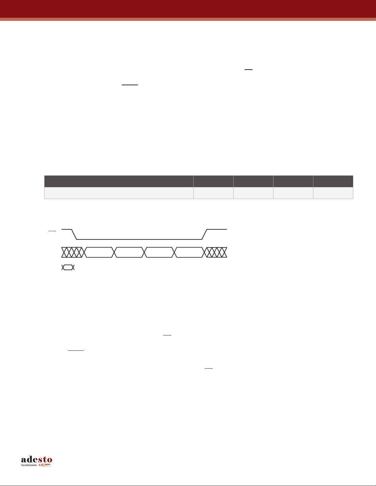
Figure 7-1. Enable Sector Protection
CS
SI
Each transition represents eight bits
3Dh 2Ah 7Fh A9h
AT45DQ321 [ADVANCE DATASHEET]
DS-45DQ321-031–DFLASH–12/2012
21
Page 22
7.1.2 Disable Sector Protection
To disable the sector protection, a 4-byte command sequence of 3Dh, 2Ah, 7Fh, and 9Ah must be clocked into the
device. After the last bit of the opcode sequence has been clocked in, the
sector protection.
Table 7-2. Disable Sector Protection Command
Command Byte 1 Byte 2 Byte 3 Byte 4
Disable Sector Protection 3Dh 2Ah 7Fh 9Ah
Figure 7-2. Disable Sector Protection
CS
CS pin must be deasserted to disable the
SI
Each transition represents eight bits
3Dh 2Ah 7Fh 9Ah
7.2 Hardware Controlled Protection
Sectors specified for protection in the Sector Protection Register and the Sector Protection Register itself can be
protected from program and erase operations by asserting the
Sector Protection Register and any sector specified for protection cannot be erased or programmed as long as the
pin is asserted. In order to modify the Sector Protection Register, the
permanently connected to GND, then the contents of the Sector Protection Register cannot be changed. If the
deasserted or permanently connected to V
The
WP pin will override the software controlled protection method but only for protecting the sectors.
Example: If the sectors were not previously protected by the Enable Sector Protection command, then simply
asserting the
WP pin is deasserted, however, the sector protection would no longer be enabled (after the maximum
specified t
asserted. If the Enable Sector Protection command was issued before or while the
then simply deasserting the
Protection command would need to be issued while the
protection. The Disable Sector Protection command is also ignored whenever the
WP pin would enable the sector protection within the maximum specified t
time) as long as the Enable Sector Protection command was not issued while the WP pin was
WPD
WP pin would not disable the sector protection. In this case, the Disable Sector
WP pin and keeping the pin in its asserted state. The
WP pin must be deasserted. If the WP pin is
, then the contents of the Sector Protection Register can be modified.
CC
time. When the
WPE
WP pin was asserted,
WP pin is deasserted to disable the sector
WP pin is asserted.
WP
WP pin is
A noise filter is incorporated to help protect against spurious noise that may inadvertently assert or deassert the
Figures 7-3 and Table 7-3 detail the sector protection status for various scenarios of the
WP pin, the Enable Sector
Protection command, and the Disable Sector Protection command.
AT45DQ321 [ADVANCE DATASHEET]
DS-45DQ321-031–DFLASH–12/2012
WP pin.
22
Page 23
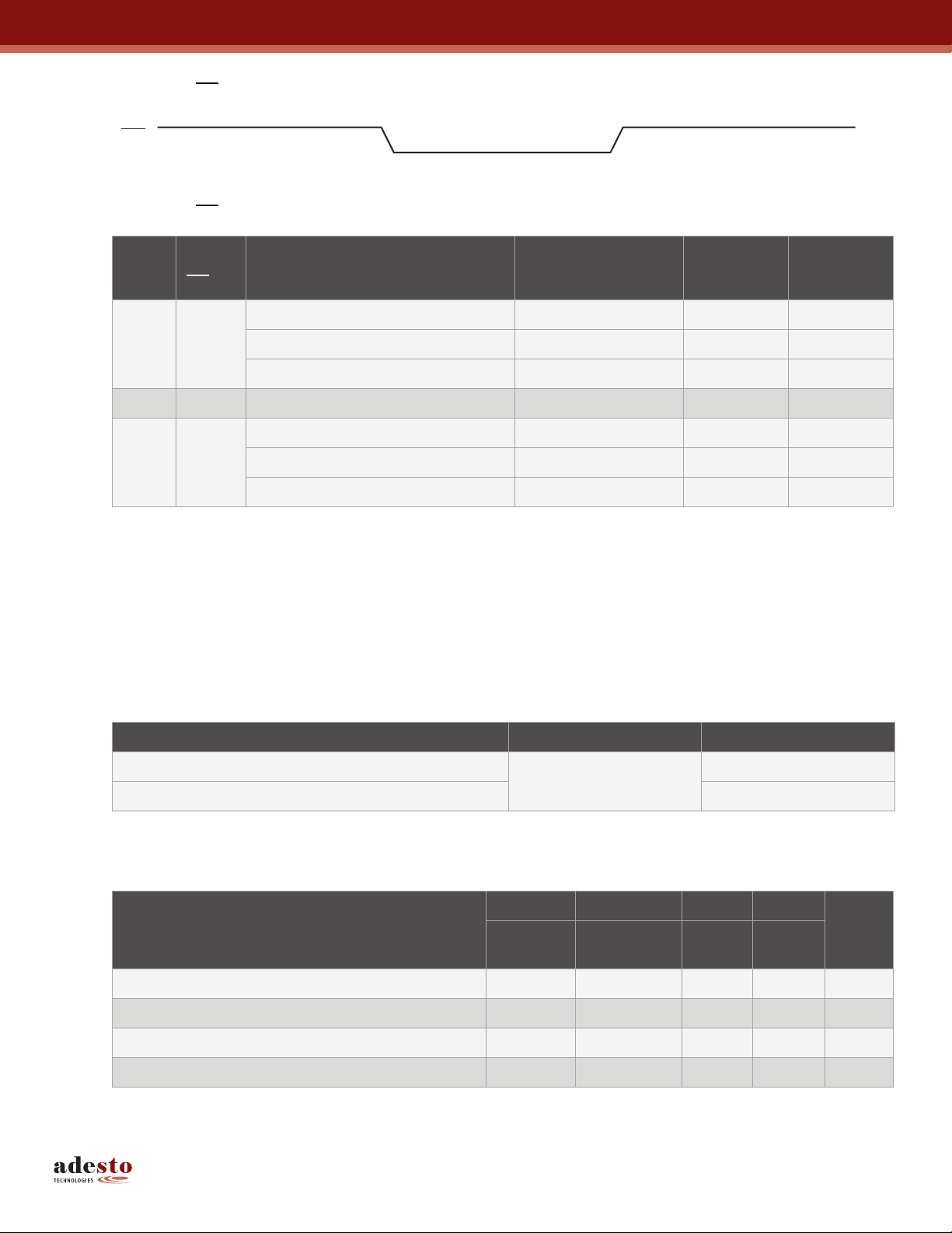
Figure 7-3. WP Pin and Protection Status
12
WP
3
Table 7-3.
Time
Period
1 High
2 Low X X Enabled Read
3 High
WP Pin and Protection Status
WP Pin Enable Sector Protection Command
Command Not Issued Previously X Disabled Read/Write
Issue Command — Enabled Read/Write
Command Issued During Period 1 or 2 Not Issued Yet Enabled Read/Write
Issue Command — Enabled Read/Write
7.3 Sector Protection Register
The nonvolatile Sector Protection Register specifies which sectors are to be protected or unprotected with either the
software or hardware controlled protection methods. The Sector Protection Register contains 64 bytes of data, of which
byte locations 0 through 63 contain values that specify whether Sectors 0 through 63 will be protected or unprotected.
The Sector Protection Register is user modifiable and must be erased before it can be reprogrammed. Table 7-4
illustrates the format of the Sector Protection Register.
Sector
Disable Sector
Protection Command
— Issue Command Disabled Read/Write
— Issue Command Disabled Read/Write
Protection
Status
Sector
Protection
Register
Table 7-4. Sector Protection Register
Sector Number 0 (0a, 0b) 1 to 63
Protected
See Table 7-5
Unprotected 00h
FFh
Note: 1. The default values for bytes 0 through 63 are 00h when shipped from Adesto.
Table 7-5. Sector 0 (0a, 0b) Sector Protection Register Byte Value
Bit 7:6 Bit 5:4 Bit 3:2 Bit 1:0
Sector 0a
(Page 0-7)
Sectors 0a and 0b Unprotected 00 00 XX XX 0xh
Protect Sector 0a 11 00 XX XX Cxh
Protect Sector 0b 00 11 XX XX 3xh
Protect Sectors 0a and 0b 11 11 XX XX Fxh
Sector 0b
(Page 8-127)
N/A N/A
Value
Note: 1. x = Don’t care
Data
AT45DQ321 [ADVANCE DATASHEET]
DS-45DQ321-031–DFLASH–12/2012
23
Page 24
7.3.1 Erase Sector Protection Register
In order to modify and change the values of the Sector Protection Register, it must first be erased using the Erase Sector
Protection Register command.
To erase the Sector Protection Register, a 4-byte command sequence of 3Dh, 2Ah, 7Fh, and CFh must be clocked into
the device. After the last bit of the opcode sequence has been clocked in, the
internally self-timed erase cycle. The erasing of the Sector Protection Register should take place in a maximum time of
. During this time, the RDY/BUSY bit in the Status Register will indicate that the device is busy. If the device is
t
PE
powered-down before the completion of the erase cycle, then the contents of the Sector Protection Register cannot be
guaranteed.
The Sector Protection Register can be erased with sector protection enabled or disabled. Since the erased state (FFh) of
each byte in the Sector Protection Register is used to indicate that a sector is specified for protection, leaving the sector
protection enabled during the erasing of the register allows the protection scheme to be more effective in the prevention
of accidental programming or erasing of the device. If for some reason an erroneous program or erase command is sent
to the device immediately after erasing the Sector Protection Register and before the register can be reprogrammed,
then the erroneous program or erase command will not be processed because all sectors would be protected.
Table 7-6. Erase Sector Protection Register Command
Command Byte 1 Byte 2 Byte 3 Byte 4
Erase Sector Protection Register 3Dh 2Ah 7Fh CFh
CS pin must be deasserted to initiate the
Figure 7-4. Erase Sector Protection Register
CS
SI
3Dh 2Ah 7Fh CFh
Each transition represents eight bits
7.3.2 Program Sector Protection Register
Once the Sector Protection Register has been erased, it can be reprogrammed using the Program Sector Protection
Register command.
To program the Sector Protection Register, a 4-byte command sequence of 3Dh, 2Ah, 7Fh, and FCh must be clocked
into the device followed by 64 bytes of data corresponding to Sectors 0 through 63. After the last bit of the opcode
sequence and data have been clocked in, the
cycle. The programming of the Sector Protection Register should take place in a maximum time of t
the RDY/
BUSY bit in the Status Register will indicate that the device is busy. If the device is powered-down before the
completion of the erase cycle, then the contents of the Sector Protection Register cannot be guaranteed.
If the proper number of data bytes is not clocked in before the
sectors corresponding to the bytes not clocked in cannot be guaranteed.
Example: If only the first two bytes are clocked in instead of the complete 64 bytes, then the protection status of the
last 62 sectors cannot be guaranteed. Furthermore, if more than 64 bytes of data is clocked into the device,
then the data will wrap back around to the beginning of the register. For instance, if 65 bytes of data are
clocked in, then the 65th byte will be stored at byte location 0 of the Sector Protection Register.
CS pin must be deasserted to initiate the internally self-timed program
. During this time,
P
CS pin is deasserted, then the protection status of the
The data bytes clocked into the Sector Protection Register need to be valid values (0xh, 3xh, Cxh, and Fxh for Sector 0a
or Sector 0b, and 00h or FFh for other sectors) in order for the protection to function correctly. If a non-valid value is
AT45DQ321 [ADVANCE DATASHEET]
DS-45DQ321-031–DFLASH–12/2012
24
Page 25
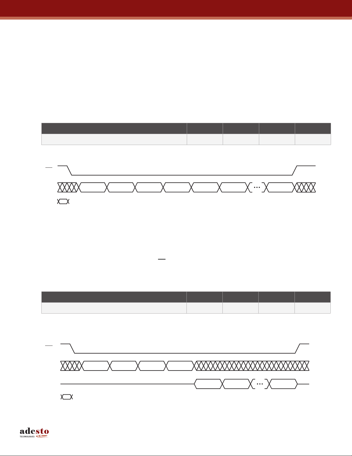
clocked into a byte location of the Sector Protection Register, then the protection status of the sector corresponding to
that byte location cannot be guaranteed.
Example: If a value of 17h is clocked into byte location 2 of the Sector Protection Register, then the protection status
of Sector 2 cannot be guaranteed.
The Sector Protection Register can be reprogrammed while the sector protection is enabled or disabled. Being able to
reprogram the Sector Protection Register with the sector protection enabled allows the user to temporarily disable the
sector protection to an individual sector rather than disabling sector protection completely.
The Program Sector Protection Register command utilizes Buffer 1 for processing. Therefore, the contents of Buffer 1
will be altered from its previous state when this command is issued.
Table 7-7. Program Sector Protection Register Command
Command Byte 1 Byte 2 Byte 3 Byte 4
Program Sector Protection Register 3Dh 2Ah 7Fh FCh
Figure 7-5. Program Sector Protection Register
CS
SI
Each transition represents eight bits
3Dh 2Ah 7Fh FCh
7.3.3 Read Sector Protection Register
To read the Sector Protection Register, an opcode of 32h and three dummy bytes must be clocked into the device. After
the last bit of the opcode and dummy bytes have been clocked in, any additional clock pulses on the SCK pin will result
in the Sector Protection Register contents being output on the SO pin. The first byte (byte location 0) corresponds to
Sector 0 (0a and 0b), the second byte corresponds to Sector 1, and the last byte (byte location 63) corresponds to Sector
63. Once the last byte of the Sector Protection Register has been clocked out, any additional clock pulses will result in
undefined data being output on the SO pin. The
Register operation and put the output into a high-impedance state.
Table 7-8. Read Sector Protection Register Command
Command Byte 1 Byte 2 Byte 3 Byte 4
Read Sector Protection Register 32h XXh XXh XXh
Note: 1. XX = Dummy byte
Figure 7-6. Read Sector Protection Register
CS
Data Byte
n
Data Byte
n + 1
Data Byte
n + 63
CS pin must be deasserted to terminate the Read Sector Protection
SI
SO
32h XX XX XX
Each transition represents eight bits
Data
n
Data
n + 1
Data
n + 63
AT45DQ321 [ADVANCE DATASHEET]
DS-45DQ321-031–DFLASH–12/2012
25
Page 26

7.3.4 About the Sector Protection Register
The Sector Protection Register is subject to a limit of 10,000 erase/program cycles. Users are encouraged to carefully
evaluate the number of times the Sector Protection Register will be modified during the course of the application’s life
cycle. If the application requires that the Security Protection Register be modified more than the specified limit of 10,000
cycles because the application needs to temporarily unprotect individual sectors (sector protection remains enabled
while the Sector Protection Register is reprogrammed), then the application will need to limit this practice. Instead, a
combination of temporarily unprotecting individual sectors along with disabling sector protection completely will need to
be implemented by the application to ensure that the limit of 10,000 cycles is not exceeded.
AT45DQ321 [ADVANCE DATASHEET]
DS-45DQ321-031–DFLASH–12/2012
26
Page 27

8. Security Features
8.1 Sector Lockdown
The device incorporates a sector lockdown mechanism that allows each individual sector to be permanently locked so
that it becomes read-only (ROM). This is useful for applications that require the ability to permanently protect a number of
sectors against malicious attempts at altering program code or security information.
Warning: Once a sector is locked down, it can never be erased or programmed, and it can never be unlocked.
To issue the sector lockdown command, a 4-byte command sequence of 3Dh, 2Ah, 7Fh, and 30h must be clocked into
the device followed by three address bytes specifying any address within the sector to be locked down. After the last
address bit has been clocked in, the
The lockdown sequence should take place in a maximum time of t
Register will indicate that the device is busy. If the device is powered-down before the completion of the lockdown
sequence, then the lockdown status of the sector cannot be guaranteed. In this case, it is recommended that the user
read the Sector Lockdown Register to determine the status of the appropriate sector lockdown bits or bytes and re-issue
the Sector Lockdown command if necessary.
Table 8-1. Sector Lockdown Command
Command Byte 1 Byte 2 Byte 3 Byte 4
Sector Lockdown 3Dh 2Ah 7Fh 30h
Figure 8-1. Sector Lockdown
CS pin must be deasserted to initiate the internally self-timed lockdown sequence.
. During this time, the RDY/BUSY bit in the Status
P
CS
SI
Each transition represents eight bits
3Dh 2Ah 7Fh 30h
8.1.1 Read Sector Lockdown Register
The nonvolatile Sector Lockdown Register specifies which sectors in the main memory are currently unlocked or have
been permanently locked down. The Sector Lockdown Register is a read-only register and contains 64 bytes of data
which correspond to Sectors 0 through 63. To read the Sector Lockdown Register, an opcode of 35h must be clocked
into the device followed by three dummy bytes. After the last bit of the opcode and dummy bytes have been clocked in,
the data for the contents of the Sector Lockdown Register will be clocked out on the SO pin. The first byte (byte
location 0) corresponds to Sector 0 (0a and 0b), the second byte corresponds to Sector 1, and the last byte (byte location
63) corresponds to Sector 63. After the last byte of the Sector Lockdown Register has been read, additional pulses on
the SCK pin will result in undefined data being output on the SO pin.
Deasserting the
CS pin will terminate the Read Sector Lockdown Register operation and put the SO pin into a
high-impedance state. Table 8-2 details the format the Sector Lockdown Register.
Table 8-2. Sector Lockdown Register
Sector Number 0 (0a, 0b) 1 to 15
Locked
Unlocked 00h
Address
byte
See Table 8-3
Address
byte
Address
byte
FFh
AT45DQ321 [ADVANCE DATASHEET]
DS-45DQ321-031–DFLASH–12/2012
27
Page 28

Table 8-3. Sector 0 (0a and 0b) Sector Lockdown Register Byte Value
Bit 7:6 Bit 5:4 Bit 3:2 Bit 1:0
Sector 0a
(Page 0-7)
Sector 0b
(Page 8-127) N/A N/A
Value
Sectors 0a and 0b Unlocked 00 00 00 00 00h
Sector 0a Locked 11 00 00 00 C0h
Sector 0b Locked 00 11 00 00 30h
Sectors 0a and 0b Locked 11 11 00 00 F0h
Table 8-4. Read Sector Lockdown Register Command
Command Byte 1 Byte 2 Byte 3 Byte 4
Read Sector Lockdown Register 35h XXh XXh XXh
Figure 8-2. Read Sector Lockdown Register
CS
Data
SI
32h XX XX XX
SO
Each transition represents eight bits
8.1.2 Freeze Sector Lockdown
The Sector Lockdown command can be permanently disabled, and the current sector lockdown state can be
permanently frozen so that no additional sectors can be locked down aside from those already locked down. Any
attempts to issue the Sector Lockdown command after the Sector Lockdown State has been frozen will be ignored.
To issue the Freeze Sector Lockdown command, the
AAh, and 40h must be clocked into the device. Any additional data clocked into the device will be ignored. When the
pin is deasserted, the current sector lockdown state will be permanently frozen within a time of t
bit in the Status Register will be permanently reset to a Logic 0 to indicate that the Sector Lockdown command is
permanently disabled.
Table 8-5. Freeze Sector Lockdown
Command Byte 1 Byte 2 Byte 3 Byte 4
Freeze Sector Lockdown 34h 55h AAh 40h
Data
n
Data
n + 1
Data
n + 63
CS pin must be asserted and the opcode sequence of 34h, 55h,
. In addition, the SLE
LOCK
CS
Figure 8-3. Freeze Sector Lockdown
CS
SI
Each transition represents eight bits
34h 55h AAh 40h
AT45DQ321 [ADVANCE DATASHEET]
DS-45DQ321-031–DFLASH–12/2012
28
Page 29

8.2 Security Register
The device contains a specialized Security Register that can be used for purposes such as unique device serialization or
locked key storage. The register is comprised of a total of 128 bytes that is divided into two portions. The first 64 bytes
(byte locations 0 through 63) of the Security Register are allocated as a One-Time Programmable space. Once these 64
bytes have been programmed, they cannot be erased or reprogrammed. The remaining 64 bytes of the register (byte
locations 64 through 127) are factory programmed by Adesto and will contain a unique value for each device. The factory
programmed data is fixed and cannot be changed.
Table 8-6. Security Register
0 1 · · · 63 64 65 · · · 127
Data Type One-Time User Programmable Factory Programmed by Adesto
8.2.1 Programming the Security Register
The user programmable portion of the Security Register does not need to be erased before it is programmed.
To program the Security Register, a 4-byte opcode sequence of 9Bh, 00h, 00h, and 00h must be clocked into the device.
After the last bit of the opcode sequence has been clocked into the device, the data for the contents of the 64-byte user
programmable portion of the Security Register must be clocked in.
After the last data byte has been clocked in, the
cycle. The programming of the Security Register should take place in a time of t
the Status Register will indicate that the device is busy. If the device is powered-down during the program cycle, then the
contents of the 64-byte user programmable portion of the Security Register cannot be guaranteed.
If the full 64 bytes of data are not clocked in before the
clocked in cannot be guaranteed.
Security Register Byte Number
CS pin must be deasserted to initiate the internally self-timed program
, during which time the RDY/BUSY bit in
P
CS pin is deasserted, then the values of the byte locations not
Example: If only the first two bytes are clocked in instead of the complete 64 bytes, then the remaining 62 bytes of the
user programmable portion of the Security Register cannot be guaranteed. Furthermore, if more than
64 bytes of data is clocked into the device, then the data will wrap back around to the beginning of the
register. For example, if 65 bytes of data are clocked in, then the 65th byte will be stored at byte location 0 of
the Security Register.
Warning: The user programmable portion of the Security Register can only be programmed one time.
Therefore, it is not possible, for example, to only program the first two bytes of the register and then program
the remaining 62 bytes at a later time.
The Program Security Register command utilizes Buffer 1 for processing. Therefore, the contents of Buffer
1 will be altered from its previous state when this command is issued.
Figure 8-4. Program Security Register
CS
SI
9Bh 00h 00h 00h
Each transition represents eight bits
Data
n
Data
n + 1
Data
n + 63
AT45DQ321 [ADVANCE DATASHEET]
DS-45DQ321-031–DFLASH–12/2012
29
Page 30

8.2.2 Reading the Security Register
To read the Security Register, an opcode of 77h and three dummy bytes must be clocked into the device. After the last
dummy bit has been clocked in, the contents of the Security Register can be clocked out on the SO pin. After the last
byte of the Security Register has been read, additional pulses on the SCK pin will result in undefined data being output
on the SO pin.
Deasserting the
CS pin will terminate the Read Security Register operation and put the SO pin into a high-impedance
state.
Figure 8-5. Read Security Register
CS
SI
SO
77h XX XX XX
Each transition represents eight bits
Data
n
Data
n + 1
Data
n + x
AT45DQ321 [ADVANCE DATASHEET]
DS-45DQ321-031–DFLASH–12/2012
30
Page 31

9. Additional Commands
9.1 Main Memory Page to Buffer Transfer
A page of data can be transferred from the main memory to either Buffer 1 or Buffer 2. To transfer a page of data using
the standard DataFlash page size (528 bytes), an opcode of 53h for Buffer 1 or 55h for Buffer 2 must be clocked into the
device followed by three address bytes comprised of 1 dummy bit, 13 page address bits (PA12 - PA0) which specify the
page in main memory to be transferred, and 10 dummy bits. To transfer a page of data using the binary page size (512
bytes), an opcode of 53h for Buffer 1 and 55h for Buffer 2 must be clocked into the device followed by three address
bytes comprised of 2 dummy bits, 13 page address bits (A21 - A9) which specify the page in the main memory to be
transferred, and 9 dummy bits.
CS pin must be low while toggling the SCK pin to load the opcode and the three address bytes from the input pin
The
(SI). The transfer of the page of data from the main memory to the buffer will begin when the
low to a high state. During the page transfer time (t
determine whether or not the transfer has been completed.
9.2 Main Memory Page to Buffer Compare
A page of data in main memory can be compared to the data in Buffer 1 or Buffer 2 as a method to ensure that data was
successfully programmed after a Buffer to Main Memory Page Program command. To compare a page of data with the
standard DataFlash page size (528 bytes), an opcode of 60h for Buffer 1 or 61h for Buffer 2 must be clocked into the
device followed by three address bytes comprised of 1 dummy bit, 13 page address bits (PA12 - PA0) which specify the
page in the main memory to be compared to the buffer, and 10 dummy bits. To compare a page of data with the binary
page size (512 bytes), an opcode of 60h for Buffer 1 or 61h for Buffer 2 must be clocked into the device followed by three
address bytes comprised of 2 dummy bits, 13 page address bits (A21 - A9) which specify the page in the main memory
to be compared to the buffer, and 9 dummy bits.
CS pin must be low while toggling the SCK pin to load the opcode and the address bytes from the input pin (SI). On
The
the low-to-high transition of the
bytes in Buffer 1 or Buffer 2. During the compare time (t
the part is busy. On completion of the compare operation, bit 6 of the Status Register will be updated with the result of the
compare.
CS pin, the data bytes in the selected Main Memory Page will be compared with the data
CS pin transitions from a
), the RDY/BUSY bit in the Status Register can be read to
XFR
), the RDY/BUSY bit in the Status Register will indicate that
COMP
9.3 Auto Page Rewrite
This command only needs to be used if the possibility exists that static (non-changing) data may be stored in a page or
pages of a sector and the other pages of the same sector are erased and programmed a large number of times.
Applications that modify data in a random fashion within a sector may fall into this category. To preserve data integrity of
a sector, each page within a sector must be updated/rewritten at least once within every 20,000 cumulative page
erase/program operations within that sector. The Auto Page Rewrite command provides a simple and efficient method to
“refresh” a page in the main memory array in a single operation.
The Auto Page Rewrite command is a combination of the Main Memory Page to Buffer Transfer and Buffer to Main
Memory Page Program with Built-In Erase commands. With the Auto Page Rewrite command, a page of data is first
transferred from the main memory to Buffer 1 or Buffer 2 and then the same data (from Buffer 1 or Buffer 2) is
programmed back into the same page of main memory, essentially “refreshing” the contents of that page. To start the
Auto Page Rewrite operation with the standard DataFlash page size (528 bytes), a 1-byte opcode, 58H for Buffer 1 or
59H for Buffer 2, must be clocked into the device followed by three address bytes comprised of 1 dummy bit, 13 page
address bits (PA12-PA0) that specify the page in main memory to be rewritten, and 10 dummy bits.
To initiate an Auto Page Rewrite with the a binary page size (512 bytes), the opcode 58H for Buffer 1 or 59H for Buffer 2,
must be clocked into the device followed by three address bytes consisting of 2 dummy bits, 13 page address bits
(A21 - A9) that specify the page in the main memory that is to be rewritten, and 9 dummy bits. When a low-to-high
transition occurs on the
CS pin, the part will first transfer data from the page in main memory to a buffer and then
AT45DQ321 [ADVANCE DATASHEET]
DS-45DQ321-031–DFLASH–12/2012
31
Page 32

program the data from the buffer back into same page of main memory. The operation is internally self-timed and should
take place in a maximum time of t
If a sector is programmed or reprogrammed sequentially page by page and the possibility does not exist that there will be
a page or pages of static data, then the programming algorithm shown in Figure 26-1 on page 72 is recommended.
Otherwise, if there is a chance that there may be a page or pages of a sector that will contain static data, then the
programming algorithm shown in Figure 26-2 on page 73 is recommended.
Please contact Adesto for availability of devices that are specified to exceed the 20,000 cycle cumulative limit.
9.4 Status Register Read
The 2-byte Status Register can be used to determine the device's ready/busy status, page size, a Main Memory Page to
Buffer Compare operation result, the sector protection status, Freeze Sector Lockdown status, erase/program error
status, Program/Erase Suspend status, and the device density. The Status Register can be read at any time, including
during an internally self-timed program or erase operation.
To read the Status Register, the
After the opcode has been clocked in, the device will begin outputting Status Register data on the SO pin during every
subsequent clock cycle. After the second byte of the Status Register has been clocked out, the sequence will repeat
itself, starting again with the first byte of the Status Register, as long as the
being pulsed. The data in the Status Register is constantly being updated, so each repeating sequence may output new
data. The RDY/
Deasserting the
state. The
BUSY status is available for both bytes of the Status Register and is updated for each byte.
CS pin will terminate the Status Register Read operation and put the SO pin into a high-impedance
CS pin can be deasserted at any time and does not require that a full byte of data be read.
. During this time, the RDY/BUSY Status Register will indicate that the part is busy.
EP
CS pin must first be asserted and then the opcode D7h must be clocked into the device.
CS pin remains asserted and the clock pin is
Table 9-1. Status Register Format – Byte 1
Bit Name
7 RDY/BUSY Ready/Busy Status R
6 COMP Compare Result R
5:2 DENSITY Density Code R 1101 32-Mbit
1 PROTECT Sector Protection Status R
0 PAGE SIZE Page Size Configuration R
Type
(1)
Description
0 Device is busy with an internal operation.
1 Device is ready.
0 Main memory page data matches buffer data.
1 Main memory page data does not match buffer data.
0 Sector protection is disabled.
1 Sector protection is enabled.
0 Device is configured for standard DataFlash page size (528 bytes).
1 Device is configured for “power of 2” binary page size (512 bytes).
Note: 1. R = Readable only
AT45DQ321 [ADVANCE DATASHEET]
DS-45DQ321-031–DFLASH–12/2012
32
Page 33

Table 9-2. Status Register Format – Byte 2
Bit Name
7 RDY/BUSY Ready/Busy Status R
6 RES Reserved for Future Use R 0 Reserved for future use.
5 EPE Erase/Program Error R
4 RES Reserved for Future Use R 0 Reserved for future use.
3 SLE Sector Lockdown Enabled R
2 PS2
1 PS1
0 ES Erase Suspend R
Program Suspend Status
(Buffer 2)
Program Suspend Status
(Buffer 1)
Type
R
R
(1)
Description
0 Device is busy with an internal operation.
1 Device is ready.
0 Erase or program operation was successful.
1 Erase or program error detected.
0 Sector Lockdown command is disabled.
1 Sector Lockdown command is enabled.
0 No program operation has been suspended while using Buffer 2.
1 A sector is program suspended while using Buffer 2.
0 No program operation has been suspended while using Buffer 1.
1 A sector is program suspended while using Buffer 1.
0 No sectors are erase suspended.
1 A sector is erase suspended.
Note: 1. R = Readable only
9.4.1 RDY/BUSY Bit
The RDY/BUSY bit is used to determine whether or not an internal operation, such as a program or erase, is in progress.
To poll the RDY/
BUSY bit to detect the completion of an internally timed operation, new Status Register data must be
continually clocked out of the device until the state of the RDY/
9.4.2 COMP Bit
The result of the most recent Main Memory Page to Buffer Compare operation is indicated using the COMP bit. If the
COMP bit is a Logic 1, then at least one bit of the data in the Main Memory Page does not match the data in the buffer.
9.4.3 DENSITY Bits
The device density is indicated using the DENSITY bits. For the AT45DQ321, the four bit binary value is 1101. The
decimal value of these four binary bits does not actually equate to the device density; the four bits represent a
combinational code relating to differing densities of DataFlash devices. The DENSITY bits are not the same as the
density code indicated in the JEDEC Device ID information. The DENSITY bits are provided only for backward
compatibility to older generation DataFlash devices.
9.4.4 PROTECT Bit
The PROTECT bit provides information to the user on whether or not the sector protection has been enabled or disabled,
either by the software-controlled method or the hardware-controlled method.
BUSY bit changes from a Logic 0 to a Logic 1.
9.4.5 PAGE SIZE Bit
The PAGE SIZE bit indicates whether the buffer size and the page size of the main memory array is configured for the
“power of 2” binary page size (512 bytes) or the standard DataFlash page size (528 bytes).
AT45DQ321 [ADVANCE DATASHEET]
DS-45DQ321-031–DFLASH–12/2012
33
Page 34

9.4.6 EPE Bit
The EPE bit indicates whether the last erase or program operation completed successfully or not. If at least one byte
during the erase or program operation did not erase or program properly, then the EPE bit will be set to the Logic 1 state.
The EPE bit will not be set if an erase or program operation aborts for any reason, such as an attempt to erase or
program a protected region or a locked down sector or an attempt to erase or program a suspended sector. The EPE bit
is updated after every erase and program operation.
9.4.7 SLE Bit
The SLE bit indicates whether or not the Sector Lockdown command is enabled or disabled. If the SLE bit is a Logic 1,
then the Sector Lockdown command is still enabled and sectors can be locked down. If the SLE bit is a Logic 0, then the
Sector Lockdown command has been disabled and no further sectors can be locked down.
9.4.8 PS2 Bit
The PS2 bit indicates if a program operation has been suspended while using Buffer 2. If the PS2 bit is a Logic 1, then a
program operation has been suspended while Buffer 2 was being used, and any command attempts that would modify
the contents of Buffer 2 will be ignored.
9.4.9 PS1 Bit
The PS1 bit indicates if a program operation has been suspended while using Buffer 1. If the PS1 bit is a Logic 1, then a
program operation has been suspended while Buffer 1 was being used, and any command attempts that would modify
the contents of Buffer 1 will be ignored.
9.4.10 The ES bit
The ES bit indicates whether or not an erase has been suspended. If the ES bit is a Logic 1, then an erase operation
(page, block, sector, or chip) has been suspended.
9.5 Read Configuration Register
The non-volatile Configuration Register can be used to determine if the Quad-input Buffer 1 or 2 Write and Quad-output
Read Array commands have been enabled. Unlike the Status Register, the Configuration Register can only be read
when the device is in an idle state (when the RDY/
state).
To read the Configuration Register, the
device. After the opcode has been clocked in, the device will begin outputting one byte of Configuration Register data on
the SO pin during subsequent clock cycles. The data being output will be a repeating byte as long as the
asserted and the clock pin is being pulsed.
At clock frequencies above f
above f
, at least two bytes of data must be clocked out from the device in order to determine the correct value of the
CLK
Configuration Register.
Deasserting the
CS pin will terminate the Read Configuration Register operation and put the SO pin into a
high-impedance state. The
The Configuration Register is a non-volatile register; therefore, the contents of the Configuration Register are not
affected by power cycles or power-on reset operations.
, the first byte of data output will not be valid. Therefore, if operating at clock frequencies
CLK
CS pin can be deasserted at any time and does not require that a full byte of data be read.
BUSY bit of the Status Register indicates that the device is in a ready
CS pin must first be asserted and the opcode of 3Fh must be clocked into the
CS pin remains
AT45DQ321 [ADVANCE DATASHEET]
DS-45DQ321-031–DFLASH–12/2012
34
Page 35

Figure 9-1. Configuration Register Format
Bit Name
7 QE Quad Enable R/W
6:0 RES Reserved for Future Use R 0 Reserved for future use.
Note: 1. Only bit seven of the Configuration Register will be modified when using the Quad Enable/Disable
9.5.1 QE Bit
The QE bit is used to control whether the Quad-input Buffer 1 Write or Buffer 2 Write and the Quad-output Read Array
commands are enabled or disabled. When the QE bit is in the Logical 1 state, the Quad-input Buffer Write and Quadoutput Read Array commands are enabled and will be recognized by the device. In addition, the
functions are disabled and the
RESET is I/O3).
and
When the QE bit is in the Logical 0 state, the Quad-Input Buffer Write and Quad-output Read Array commands are
disabled and will not be recognized by the device as valid commands and the
control pins. The
The Reset command has no effect on the QE bit. The QE bit defaults to the Logical 0 state when devices are initially
shipped from Adesto.
Description
Type
0 Quad-input/output commands and operation disabled.
Quad-input/output commands and operation enabled. (WP and
1
RESET disabled)
commands.
WP and RESET
WP and RESET pins themselves operate as a bidirectional input/output pins (WP is I/O2
WP and RESET pins function as normal
WP and RESET pins should be externally pulled-high to avoid erroneous or unwanted device operation.
Figure 9-2. Read Configuration Register
CS
2310
675410119812 212217 20191815 1613 14 23 24
SCK
Opcode
SI
SO
00111111
MSB
High-impedance
Configuration
Register Out
XXXXXX DXXD
MSB MSB
MSB
Configuration
Register Out
XXXXXXXD
AT45DQ321 [ADVANCE DATASHEET]
DS-45DQ321-031–DFLASH–12/2012
35
Page 36

9.6 Write Configuration Register
The Write Configuration Register commands are used to modify the QE bit of the non-volatile Configuration Register.
There are two commands that are utilized to enable and disable the Quad I/O functionality of the device and they are the
Quad Enable and Quad Disable commands, respectively.
The Configuration Register is a non-volatile register and is subject to the same program/erase endurance characteristics
of the Main Memory Array. The programming of the Configuration Register is internally self-timed and should take place
in a time of t
that the device is busy. For faster throughput, it is recommended that the Status Register be polled rather than waiting
the t
time to determine if the Configuration Register has completed the programming cycle.
WRCR
The Write Configuration Register (Quad Enable and Quad Disable) is subject to a limit of 10,000 cycles. Users are
encouraged to carefully evaluate the number of times the Write Configuration Register will be modified during the course
of the application’s life cycle.
9.6.1 Quad Enable Command
The Quad Enable command is used to program the QE bit of the non-volatile Configuration Register to a Logical 1 to
enable the Quad I/O functionality of the device. To issue the Quad Enable command, the
followed by a four byte opcode of 3Dh, 2Ah, 81h, and 66h.
After the last bit of the four byte opcode has been clocked in, the
Configuration Register to be modified within the time of t
Table 9-3. Quad Enable Command
While the Configuration Register is being updated, the Status Register can be read and will indicate
WRCR.
WRCR
CS pin must first be asserted
CS pin must be deasserted allowing the QE bit of the
.
Command Byte 1 Byte 2 Byte 3 Byte 4
Quad Enable 3Dh 2Ah 81h 66h
Figure 9-3. Quad Enable
CS
SI
Each transition represents eight bits
3Dh 2Ah 81h 66h
AT45DQ321 [ADVANCE DATASHEET]
DS-45DQ321-031–DFLASH–12/2012
36
Page 37

9.6.2 Quad Disable Command
The Quad Disable command is used to program the QE bit of the non-volatile Configuration Register to a Logical 0 to
disable the Quad I/O functionality of the device. To issue the Quad Disable command, the
followed by a four byte opcode of 3Dh, 2Ah, 81h and 67h.
After the last bit of the four byte opcode has been clocked in, the
Configuration Register to be modified within the time of t
Table 9-4. Quad Disable Command
Command Byte 1 Byte 2 Byte 3 Byte 4
Quad Disable 3Dh 2Ah 81h 67h
Figure 9-4. Quad Disable
CS
WRCR
CS pin must first be asserted
CS pin must be deasserted allowing the QE bit of the
.
SI
3Dh 2Ah 81h 67h
Each transition represents eight bits
AT45DQ321 [ADVANCE DATASHEET]
DS-45DQ321-031–DFLASH–12/2012
37
Page 38

10. Deep Power-Down
During normal operation, the device will be placed in the standby mode to consume less power as long as the CS pin
remains deasserted and no internal operation is in progress. The Deep Power-Down command offers the ability to place
the device into an even lower power consumption state called the Deep Power-Down mode.
When the device is in the Deep Power-Down mode, all commands including the Status Register Read command will be
ignored with the exception of the Resume from Deep Power-Down command. Since all commands will be ignored, the
mode can be used as an extra protection mechanism against program and erase operations.
Entering the Deep Power-Down mode is accomplished by simply asserting the
then deasserting the
pin is deasserted, the device will enter the Deep Power-Down mode within the maximum time of t
The complete opcode must be clocked in before the
even byte boundary (multiples of eight bits); otherwise, the device will abort the operation and return to the standby mode
once the
CS pin is deasserted. In addition, the device will default to the standby mode after a power cycle.
The Deep Power-Down command will be ignored if an internally self-timed operation such as a program or erase cycle is
in progress. The Deep Power-Down command must be reissued after the internally self-timed operation has been
completed in order for the device to enter the Deep Power-Down mode.
Figure 10-1. Deep Power-Down
CS pin. Any additional data clocked into the device after the opcode will be ignored. When the CS
CS pin, clocking in the opcode B9h, and
.
EDPD
CS pin is deasserted, and the CS pin must be deasserted on an
CS
SCK
SI
SO
I
CC
2310
Opcode
10111001
MSB
High-impedance
Active Current
Standby Mode Current
t
EDPD
6754
Deep Power-Down Mode Current
AT45DQ321 [ADVANCE DATASHEET]
DS-45DQ321-031–DFLASH–12/2012
38
Page 39

10.1 Resume from Deep Power-Down
In order to exit the Deep Power-Down mode and resume normal device operation, the Resume from Deep Power-Down
command must be issued. The Resume from Deep Power-Down command is the only command that the device will
recognize while in the Deep Power-Down mode.
To resume from the Deep Power-Down mode, the
clocked into the device. Any additional data clocked into the device after the opcode will be ignored. When the
deasserted, the device will exit the Deep Power-Down mode and return to the standby mode within the maximum time of
. After the device has returned to the standby mode, normal command operations such as Continuous Array Read
t
RDPD
can be resumed.
If the complete opcode is not clocked in before the
byte boundary (multiples of eight bits), then the device will abort the operation and return to the Deep Power-Down
mode.
Figure 10-2. Resume from Deep Power-Down
CS pin must first be asserted and then the opcode ABh must be
CS pin is
CS pin is deasserted, or if the CS pin is not deasserted on an even
CS
SCK
SI
SO
I
CC
2310
Opcode
10101011
MSB
High-impedance
Active Current
Deep Power-Down Mode Current
6754
t
RDPD
Standby Mode Current
AT45DQ321 [ADVANCE DATASHEET]
DS-45DQ321-031–DFLASH–12/2012
39
Page 40

10.2 Ultra-Deep Power-Down
The Ultra-Deep Power-Down mode allows the device to consume far less power compared to the standby and Deep
Power-Down modes by shutting down additional internal circuitry. Since almost all active circuitry is shutdown in this
mode to conserve power, the contents of the SRAM buffers cannot be maintained. Therefore, any data stored in the
SRAM buffers will be lost once the device enters the Ultra-Deep Power-Down mode.
When the device is in the Ultra-Deep Power-Down mode, all commands including the Status Register Read and Resume
from Deep Power-Down commands will be ignored. Since all commands will be ignored, the mode can be used as an
extra protection mechanism against program and erase operations.
Entering the Ultra-Deep Power-Down mode is accomplished by simply asserting the
and then deasserting the
CS pin is deasserted, the device will enter the Ultra-Deep Power-Down mode within the maximum time of t
The complete opcode must be clocked in before the
even byte boundary (multiples of eight bits); otherwise, the device will abort the operation and return to the standby mode
once the
CS pin is deasserted. In addition, the device will default to the standby mode after a power cycle.
The Ultra-Deep Power-Down command will be ignored if an internally self-timed operation such as a program or erase
cycle is in progress. The Ultra-Deep Power-Down command must be reissued after the internally self-timed operation
has been completed in order for the device to enter the Ultra-Deep Power-Down mode.
Figure 10-3. Ultra-Deep Power-Down
CS pin. Any additional data clocked into the device after the opcode will be ignored. When the
CS pin, clocking in the opcode 79h,
.
EUDPD
CS pin is deasserted, and the CS pin must be deasserted on an
CS
SCK
SI
SO
I
CC
2310
Opcode
0
1111001
MSB
High-impedance
Active Current
Standby Mode Current
t
EUDPD
6754
Ultra-Deep Power-Down Mode Current
AT45DQ321 [ADVANCE DATASHEET]
DS-45DQ321-031–DFLASH–12/2012
40
Page 41

10.2.1 Exit Ultra-Deep Power-Down
To exit from the Ultra-Deep Power-Down mode, the CS pin must simply be pulsed by asserting the CS pin, waiting the
minimum necessary t
time, and then deasserting the CS pin again. To facilitate simple software development, a
CSLU
dummy byte opcode can also be entered while the
Suspend operation; the dummy byte opcode is simply ignored by the device in this case. After the
deasserted, the device will exit from the Ultra-Deep Power-Down mode and return to the standby mode within a
maximum time of t
. If the CS pin is reasserted before the t
XUDPD
operation, then that operation will be ignored and nothing will be performed. The system must wait for the device to return
to the standby mode before normal command operations such as Continuous Array Read can be resumed.
Since the contents of the SRAM buffers cannot be maintained while in the Ultra-Deep Power-Down mode, the SRAM
buffers will contain undefined data when the device returns to the standby mode.
Figure 10-4. Exit Ultra-Deep Power-Down
CS pin is being pulsed just as in a normal operation like the Program
CS pin has been
time has elapsed in an attempt to start a new
XUDPD
CS
SO
I
CC
t
CSLU
t
High-impedance
Ultra-Deep Power-Down Mode Current
XUDPD
Active Current
Standby Mode Current
AT45DQ321 [ADVANCE DATASHEET]
DS-45DQ321-031–DFLASH–12/2012
41
Page 42

11. Buffer and Page Size Configuration
The memory array of DataFlash devices is actually larger than other Serial Flash devices in that extra user-accessible
bytes are provided in each page of the memory array. For the AT45DQ321, there are an extra 16 bytes of memory in
each page for a total of an extra 128KB (1-Mbits) of user-accessible memory. Therefore, the device density is actually
33-Mbits instead of 32-Mbits.
Some applications, however, may not want to take advantage of this extra memory and instead architect their software to
operate on a “power of 2” binary, logical addressing scheme. To allow this, the DataFlash can be configured so that the
buffer and page sizes are 512 bytes instead of the standard 528 bytes. In addition, the configuration of the buffer and
page sizes is reversible and can be changed from 528 bytes to 512 bytes or from 512 bytes to 528 bytes. The configured
setting is stored in an internal nonvolatile register so that the buffer and page size configuration is not affected by power
cycles. The nonvolatile register has a limit of 10,000 erase/program cycles; therefore, care should be taken to not switch
between the size options more than 10,000 times.
Devices are initially shipped from Adesto with the buffer and page sizes set to 528 bytes. Devices can be ordered from
Adesto pre-configured for the “power of 2” binary size of 512 bytes. For details, see Section 27., Ordering Information on
page 74.
To configure the device for “power of 2” binary page size (512 bytes), a 4-byte opcode sequence of 3Dh, 2Ah, 80h, and
A6h must be clocked into the device. After the last bit of the opcode sequence has been clocked in, the CS pin must be
deasserted to initiate the internally self-timed configuration process and nonvolatile register program cycle. The
programming of the nonvolatile register should take place in a time of t
Status Register will indicate that the device is busy. The device does not need to be power cycled after the completion of
the configuration process and register program cycle in order for the buffer and page size to be configured to 512 bytes.
To configure the device for standard DataFlash page size (528 bytes), a 4-byte opcode sequence of 3Dh, 2Ah, 80h, and
A7h must be clocked into the device. After the last bit of the opcode sequence has been clocked in, the
deasserted to initial the internally self-timed configuration process and nonvolatile register program cycle. The
programming of the nonvolatile register should take place in a time of t
Status Register will indicate that the device is busy. The device does not need to be power cycled after the completion of
the configuration process and register program cycle in order for the buffer and page size to be configured to 528 bytes.
, during which time the RDY/BUSY bit in the
EP
CS pin must be
, during which time the RDY/BUSY bit in the
EP
Table 11-1. Buffer and Page Size Configuration Commands
Command Byte 1 Byte 2 Byte 3 Byte 4
“Power of 2” binary page size (512 bytes) 3Dh 2Ah 80h A6h
DataFlash page size (528 bytes) 3Dh 2Ah 80h A7h
Figure 11-1. Buffer and Page Size Configuration
CS
SI
3Dh 2Ah 80h
Each transition represents eight bits
Opcode
Byte 4
AT45DQ321 [ADVANCE DATASHEET]
DS-45DQ321-031–DFLASH–12/2012
42
Page 43

12. Manufacturer and Device ID Read
Identification information can be read from the device to enable systems to electronically query and identify the device
while it is in the system. The identification method and the command opcode comply with the JEDEC Standard for
“Manufacturer and Device ID Read Methodology for SPI Compatible Serial Interface Memory Devices”. The type of
information that can be read from the device includes the JEDEC-defined Manufacturer ID, the vendor-specific
Device ID, and the vendor-specific Extended Device Information.
The Read Manufacturer and Device ID command is limited to a maximum clock frequency of f
devices are capable of operating at very high clock frequencies, applications should be designed to read the
identification information from the devices at a reasonably low clock frequency to ensure that all devices to be used in the
application can be identified properly. Once the identification process is complete, the application can then increase the
clock frequency to accommodate specific Flash devices that are capable of operating at the higher clock frequencies.
To read the identification information, the CS pin must first be asserted and then the opcode 9Fh must be clocked into
the device. After the opcode has been clocked in, the device will begin outputting the identification data on the SO pin
during the subsequent clock cycles. The first byte to be output will be the Manufacturer ID, followed by two bytes of the
Device ID information. The fourth byte output will be the Extended Device Information (EDI) String Length, which will be
01h indicating that one byte of EDI data follows. After the one byte of EDI data is output, the SO pin will go into a
high-impedance state; therefore, additional clock cycles will have no affect on the SO pin and no data will be output. As
indicated in the JEDEC Standard, reading the EDI String Length and any subsequent data is optional.
Deasserting the
high-impedance state. The
Table 12-1. Manufacturer and Device ID Information
CS pin will terminate the Manufacturer and Device ID Read operation and put the SO pin into a
CS pin can be deasserted at any time and does not require that a full byte of data be read.
. Since not all Flash
CLK
Byte No. Data Type Value
1 Manufacturer ID 1Fh
2 Device ID (Byte 1) 27h
3 Device ID (Byte 2) 00h
4 [Optional to Read] Extended Device Information (EDI) String Length 01h
5 [Optional to Read] EDI Byte 1 00h
Table 12-2. Manufacturer and Device ID Details
Hex
Data Type Bit 7 Bit 6 Bit 5 Bit 4 Bit 3 Bit 2 Bit 1 Bit 0
JEDEC Assigned Code
Manufacturer ID
0 0 0 1 1 1 1 1
Family Code Density Code
Device ID (Byte 1)
0 0 1 0 0 1 1 1
Sub Code Product Variant
Device ID (Byte 2)
0 0 0 0 0 0 0 0
Value Details
1Fh JEDEC code: 0001 1111 (1Fh for Adesto)
Family code: 001 (AT45Dxxx Family)
27h
Density code: 00111 (32-Mbit)
Sub code: 000 (Standard Series)
00h
Product variant:00000
AT45DQ321 [ADVANCE DATASHEET]
DS-45DQ321-031–DFLASH–12/2012
43
Page 44

Table 12-3. EDI Data
Byte Number Bit 7 Bit 6 Bit 5 Bit 4 Bit 3 Bit 2 Bit 1 Bit 0
Hex
Value Details
1
RFU Device Revision
0 0 0 0 0 0 0 0
Figure 12-1. Read Manufacturer and Device ID
CS
60
87 46
14 1615 22 2423 38 403930 3231
SCK
Opcode
SI
SO
High-impedance
Note: Each transition shown for SI and SO represents one byte (8 bits)
9Fh
1Fh 00h 01h 00h
Manufacturer ID Device ID
27h
Byte 1
Device ID
Byte 2
RFU: Reserved for Future Use
00h
Device revision:00000 (Initial Version)
EDI
String Length
EDI
Data Byte 1
AT45DQ321 [ADVANCE DATASHEET]
DS-45DQ321-031–DFLASH–12/2012
44
Page 45

13. Software Reset
In some applications, it may be necessary to prematurely terminate a program or erase cycle early rather than wait the
hundreds of microseconds or milliseconds necessary for the program or erase operation to complete normally. The
Software Reset command allows a program or erase operation in progress to be ended abruptly and returns the device
to an idle state.
To perform a Software Reset, the
must be clocked into the device. Any additional data clocked into the device after the last byte will be ignored. When the
CS pin is deasserted, the program or erase operation currently in progress will be terminated within a time t
the program or erase operation may not complete before the device is reset, the contents of the page being programmed
or erased cannot be guaranteed to be valid.
The Software Reset command has no effect on the states of the Sector Protection Register, the Sector Lockdown
Register, or the buffer and page size configuration. The PS2, PS1, and ES bits of the Status Register, however, will be
reset back to their default states. If a Software Reset operation is performed while a sector is erase suspended, the
suspend operation will abort and the contents of the page or block being erased in the suspended sector will be left in an
undefined state. If a Software Reset is performed while a sector is program suspended, the suspend operation will abort
and the contents of the page that was being programmed and subsequently suspended will be undefined. The remaining
pages in the sector will retain their previous contents.
The complete 4-byte opcode must be clocked into the device before the CS pin is deasserted, and the CS pin must be
deasserted on a byte boundary (multiples of eight bits); otherwise, no reset operation will be performed.
Table 13-1. Software Reset
CS pin must be asserted and a 4-byte command sequence of F0h, 00h, 00h, and 00h
. Since
SWRST
Command Byte 1 Byte 2 Byte 3 Byte 4
Software Reset F0h 00h 00h 00h
Figure 13-1. Software Reset
CS
SI
Each transition represents eight bits
F0h 00h 00h 00h
AT45DQ321 [ADVANCE DATASHEET]
DS-45DQ321-031–DFLASH–12/2012
45
Page 46

14. Operation Mode Summary
The commands described previously can be grouped into four different categories to better describe which commands
can be executed at what times.
Group A commands consist of:
1. Main Memory Page Read
2. Continuous Array Read (SPI)
3. Read Sector Protection Register
4. Read Sector Lockdown Register
5. Read Security Register
6. Read Configuration Register
Group B commands consist of:
1. Page Erase
2. Block Erase
3. Sector Erase
4. Chip Erase
5. Main Memory Page to Buffer 1 (or 2) Transfer
6. Main Memory Page to Buffer 1 (or 2) Compare
7. Buffer 1 (or 2) to Main Memory Page Program with Built-In Erase
8. Buffer 1 (or 2) to Main Memory Page Program without Built-In Erase
9. Main Memory Page Program through Buffer 1 (or 2) with Built-In Erase
10. Main Memory Byte/Page Program through Buffer 1 without Built-In Erase
11. Auto Page Rewrite
Group C commands consist of:
1. Buffer 1 (or 2) Read
2. Buffer 1 (or 2) Write
3. Status Register Read
4. Manufacturer and Device ID Read
Group D commands consist of:
1. Erase Sector Protection Register
2. Program Sector Protection Register
3. Sector Lockdown
4. Program Security Register
5. Buffer and Page Size Configuration
6. Freeze Sector Lockdown
If a Group A command is in progress (not fully completed), then another command in Group A, B, C, or D should not be
started. However, during the internally self-timed portion of Group B commands, any command in Group C can be
executed. The Group B commands using Buffer 1 should use Group C commands using Buffer 2 and vice versa. Finally,
during the internally self-timed portion of a Group D command, only the Status Register Read command should be
executed.
Most of the commands in Group B can be suspended and resumed, except the Buffer Transfer, Buffer Compare, and
Auto Page Rewrite operations. If a Group B command is suspended, all of the Group A commands can be executed. See
Table 6-4 to determine which of the Group B, Group C, and Group D commands are allowed.
AT45DQ321 [ADVANCE DATASHEET]
DS-45DQ321-031–DFLASH–12/2012
46
Page 47

15. Command Tables
Table 15-1. Read Commands
Command Opcode
Main Memory Page Read D2h
Continuous Array Read (Low Power Mode) 01h
Continuous Array Read (Low Frequency) 03h
Continuous Array Read (High Frequency) 0Bh
Continuous Array Read (High Frequency) 1Bh
Dual-output Read Array 3Bh
Quad-output Read Array 6Bh
Continuous Array Read (Legacy Command – Not Recommended for New Designs) E8h
Buffer 1 Read (Low Frequency) D1h
Buffer 2 Read (Low Frequency) D3h
Buffer 1 Read (High Frequency) D4h
Buffer 2 Read (High Frequency) D6h
Table 15-2. Program and Erase Commands
Command Opcode
Buffer 1 Write 84h
Buffer 2 Write 87h
Dual-input Buffer 1 Write 24h
Dual-input Buffer 2 Write 27h
Quad-input Buffer 1 Write 44h
Quad-input Buffer 2 Write 47h
Buffer 1 to Main Memory Page Program with Built-In Erase 83h
Buffer 2 to Main Memory Page Program with Built-In Erase 86h
Buffer 1 to Main Memory Page Program without Built-In Erase 88h
Buffer 2 to Main Memory Page Program without Built-In Erase 89h
Main Memory Page Program through Buffer 1 with Built-In Erase 82h
Main Memory Page Program through Buffer 2 with Built-In Erase 85h
Main Memory Byte/Page Program through Buffer 1 without Built-In Erase 02h
Page Erase 81h
Block Erase 50h
Sector Erase 7Ch
Chip Erase C7h + 94h + 80h + 9Ah
Program/Erase Suspend B0h
Program/Erase Resume D0h
AT45DQ321 [ADVANCE DATASHEET]
DS-45DQ321-031–DFLASH–12/2012
47
Page 48

Table 15-3. Protection and Security Commands
Command Opcode
Enable Sector Protection 3Dh + 2Ah + 7Fh + A9h
Disable Sector Protection 3Dh + 2Ah + 7Fh + 9Ah
Erase Sector Protection Register 3Dh + 2Ah + 7Fh + CFh
Program Sector Protection Register 3Dh + 2Ah + 7Fh + FCh
Read Sector Protection Register 32h
Sector Lockdown 3Dh + 2Ah + 7Fh + 30h
Read Sector Lockdown Register 35h
Freeze Sector Lockdown 34h + 55h + AAh + 40h
Program Security Register 9Bh + 00h + 00h + 00h
Read Security Register 77h
Table 15-4. Additional Commands
Command Opcode
Main Memory Page to Buffer 1 Transfer 53h
Main Memory Page to Buffer 2 Transfer 55h
Main Memory Page to Buffer 1 Compare 60h
Main Memory Page to Buffer 2 Compare 61h
Auto Page Rewrite through Buffer 1 58h
Auto Page Rewrite through Buffer 2 59h
Deep Power-Down B9h
Resume from Deep Power-Down ABh
Ultra-Deep Power-Down 79h
Status Register Read D7h
Manufacturer and Device ID Read 9Fh
Read Configuration Register 3Fh
Quad Enable 3Dh + 2Ah + 81h + 66h
Quad Disable 3Dh + 2Ah + 81h + 67h
Configure “Power of 2” (Binary) Page Size 3Dh + 2Ah + 80h + A6h
Configure Standard DataFlash Page Size 3Dh + 2Ah + 80h + A7h
Software Reset F0h + 00h + 00h + 00h
AT45DQ321 [ADVANCE DATASHEET]
DS-45DQ321-031–DFLASH–12/2012
48
Page 49

Table 15-5. Legacy Commands
(1)(2)
Command Opcode
Buffer 1 Read 54H
Buffer 2 Read 56H
Main Memory Page Read 52H
Continuous Array Read 68H
Status Register Read 57H
Note: 1. Legacy commands are not recommended for new designs.
2. Legacy commands operate from 2.30V to 3.60V Vcc only.
Table 15-6. Detailed Bit-level Addressing Sequence for Binary Page Size (512 bytes)
Page Size = 512 bytes Address Byte Address Byte Address Byte
Opcode Opcode
01h 0 0 0 0 0 0 0 1 X X A A A A A A A A A A A A A A A A A A A A A A N/A
02h 0 0 0 0 0 0 1 0 X X A A A A A A A A A A A A A A A A A A A A A A N/A
03h 0 0 0 0 0 0 1 1 X X A A A A A A A A A A A A A A A A A A A A A A N/A
0Bh 0 0 0 0 1 0 1 1 X X A A A A A A A A A A A A A A A A A A A A A A 1
1Bh 0 0 0 1 1 0 1 1 X X A A A A A A A A A A A A A A A A A A A A A A 2
24h 0 0 1 0 0 1 0 0 X X X X X X X X X X X X X X X A A A A A A A A A N/A
27h 0 0 1 0 0 1 1 1 X X X X X X X X X X X X X X X A A A A A A A A A N/A
32h 0 0 1 1 0 0 1 0 X X X X X X X X X X X X X X X X X X X X X X X X N/A
35h 0 0 1 1 0 1 0 1 X X X X X X X X X X X X X X X X X X X X X X X X N/A
3Bh 0 0 1 1 1 0 1 1 X X A A A A A A A A A A A A A A A A A A A A A A 1
3Fh 0 0 1 1 1 1 1 1 X X X X X X X X X X X X X X X X X X X X X X X X N/A
44h 0 1 0 0 0 1 0 0 X X X X X X X X X X X X X X X A A A A A A A A A N/A
47h 0 1 0 0 0 1 1 1 X X X X X X X X X X X X X X X A A A A A A A A A N/A
50h 0 1 0 1 0 0 0 0 X X A A A A A A A A A A X X X X X X X X X X X X N/A
53h 0 1 0 1 0 0 1 1 X X A A A A A A A A A A A A A X X X X X X X X X N/A
55h 0 1 0 1 0 1 0 1 X X A A A A A A A A A A A A A X X X X X X X X X N/A
58h 0 1 0 1 1 0 0 0 X X A A A A A A A A A A A A A X X X X X X X X X N/A
59h 0 1 0 1 1 0 0 1 X X A A A A A A A A A A A A A X X X X X X X X X N/A
60h 0 1 1 0 0 0 0 0 X X A A A A A A A A A A A A A X X X X X X X X X N/A
61h 0 1 1 0 0 0 0 1 X X A A A A A A A A A A A A A X X X X X X X X X N/A
6Bh 0 1 1 0 1 0 1 1 X X A A A A A A A A A A A A A A A A A A A A A A 1
77h 0 1 1 1 0 1 1 1 X X X X X X X X X X X X X X X X X X X X X X X X N/A
79h 0 1 1 1 1 0 0 1 N/A N/A N/A N/A
7Ch 0 1 1 1 1 1 0 0 X X A A A A A A X X X X X X X X X X X X X X X X N/A
81h 1 0 0 0 0 0 0 1 X X A A A A A A A A A A A A A X X X X X X X X X N/A
82h 1 0 0 0 0 0 1 0 X X A A A A A A A A A A A A A A A A A A A A A A N/A
83h 1 0 0 0 0 0 1 1 X X A A A A A A A A A A A A A X X X X X X X X X N/A
84h 1 0 0 0 0 1 0 0 X X X X X X X X X X X X X X X A A A A A A A A A N/A
85h 1 0 0 0 0 1 0 1 X X A A A A A A A A A A A A A A A A A A A A A A N/A
86h 1 0 0 0 0 1 1 0 X X A A A A A A A A A A A A A X X X X X X X X X N/A
87h 1 0 0 0 0 1 1 1 X X X X X X X X X X X X X X X A A A A A A A A A N/A
88h 1 0 0 0 1 0 0 0 X X A A A A A A A A A A A A A X X X X X X X X X N/A
Reserved
Reserved
A21
A20
A19
A18
A17
A16
A15
A14
A13
A12
A11
A10
A9
A8
A7
A6 A5A4 A3A2 A1A0
Additional
Dummy
Bytes
AT45DQ321 [ADVANCE DATASHEET]
DS-45DQ321-031–DFLASH–12/2012
49
Page 50

Page Size = 512 bytes Address Byte Address Byte Address Byte
Opcode Opcode
89h 1 0 0 0 1 0 0 1 X X A A A A A A A A A A A A A X X X X X X X X X N/A
9Fh 1 0 0 1 1 1 1 1 N/A N/A N/A N/A
B9h 1 0 1 1 1 0 0 1 N/A N/A N/A N/A
ABh 1 0 1 0 1 0 1 1 N/A N/A N/A N/A
B0h 1 0 1 1 0 0 0 0 N/A N/A N/A N/A
D0h 1 1 0 1 0 0 0 0 N/A N/A N/A N/A
D1h 1 1 0 1 0 0 0 1 X X X X X X X X X X X X X X X A A A A A A A A A N/A
D2h 1 1 0 1 0 0 1 0 X X A A A A A A A A A A A A A A A A A A A A A A 4
D3h 1 1 0 1 0 0 1 1 X X X X X X X X X X X X X X X A A A A A A A A A N/A
D4h 1 1 0 1 0 1 0 0 X X X X X X X X X X X X X X X A A A A A A A A A 1
D6h 1 1 0 1 0 1 1 0 X X X X X X X X X X X X X X X A A A A A A A A A 1
D7h 1 1 0 1 0 1 1 1 N/A N/A N/A N/A
Reserved
Reserved
A21
A20
A19
A18
A17
A16
A15
A14
A13
A12
A11
A10
A9
A8
A7
A6 A5A4 A3A2 A1A0
Note: X = Dummy Bit
Table 15-7. Detailed Bit-level Addressing Sequence for Standard DataFlash Page Size (528 bytes)
Page Size = 528-bytes Address Byte Address Byte Address Byte
Opcode Opcode
01h 0 0 0 0 0 0 0 1 X P P P P P P P P P P P P P B B B B B B B B B B N/A
02h 0 0 0 0 0 0 1 0 X P P P P P P P P P P P P P B B B B B B B B B B N/A
03h 0 0 0 0 0 0 1 1 X P P P P P P P P P P P P P B B B B B B B B B B N/A
0Bh 0 0 0 0 1 0 1 1 X P P P P P P P P P P P P P B B B B B B B B B B 1
1Bh 0 0 0 1 1 0 1 1 X P P P P P P P P P P P P P B B B B B B B B B B
24h 0 0 1 0 0 1 0 0 X X X X X X X X X X X X X X B B B B B B B B B B N/A
27h 0 0 1 0 0 1 1 1 X X X X X X X X X X X X X X B B B B B B B B B B N/A
32h 0 0 1 1 0 0 1 0 X X X X X X X X X X X X X X X X X X X X X X X X N/A
35h 0 0 1 1 0 1 0 1 X X X X X X X X X X X X X X X X X X X X X X X X N/A
3Bh 0 0 1 1 1 0 1 1 X P P P P P P P P P P P P P B B B B B B B B B B
3Fh 0 0 1 1 1 1 1 1 X X X X X X X X X X X X X X X X X X X X X X X X N/A
44h 0 1 0 0 0 1 0 0 X X X X X X X X X X X X X X X X X X X X X X X X N/A
47h 0 1 0 0 0 1 1 1 X X X X X X X X X X X X X X X X X X X X X X X X N/A
50h 0 1 0 1 0 0 0 0 X P P P P P P P P P P X X X X X X X X X X X X X N/A
53h 0 1 0 1 0 0 1 1 X P P P P P P P P P P P P P X X X X X X X X X X N/A
55h 0 1 0 1 0 1 0 1 X P P P P P P P P P P P P P X X X X X X X X X X N/A
58h 0 1 0 1 1 0 0 0 X P P P P P P P P P P P P P X X X X X X X X X X N/A
59h 0 1 0 1 1 0 0 1 X P P P P P P P P P P P P P X X X X X X X X X X N/A
60h 0 1 1 0 0 0 0 0 X P P P P P P P P P P P P P X X X X X X X X X X N/A
61h 0 1 1 0 0 0 0 1 X P P P P P P P P P P P P P X X X X X X X X X X N/A
6Bh 0 1 1 0 1 0 1 1 X P P P P P P P P P P P P P B B B B B B B B B B
77h 0 1 1 1 0 1 1 1 X X X X X X X X X X X X X X X X X X X X X X X X N/A
79h 0 1 1 1 1 0 0 1 N/A N/A N/A N/A
7Ch 0 1 1 1 1 1 0 0 X P P P P P P X X X X X X X X X X X X X X X X X N/A
81h 1 0 0 0 0 0 0 1 X P P P P P P P P P P P P P X X X X X X X X X X N/A
82h 1 0 0 0 0 0 1 0 X P P P P P P P P P P P P P B B B B B B B B B B N/A
83h 1 0 0 0 0 0 1 1 X P P P P P P P P P P P P P X X X X X X X X X X N/A
Reserved
PA12
PA11
PA10
PA9
PA8
PA7
PA6
PA5
PA4
PA3
PA2
PA1
PA0
BA9
BA8
BA7
BA6
BA5
BA4
BA3
BA2
BA1
Additional
Dummy
Bytes
Additional
Dummy
Bytes
BA0
2
1
1
AT45DQ321 [ADVANCE DATASHEET]
DS-45DQ321-031–DFLASH–12/2012
50
Page 51

Page Size = 528-bytes Address Byte Address Byte Address Byte
Opcode Opcode
84h 1 0 0 0 0 1 0 0 X X X X X X X X X X X X X X B B B B B B B B B B N/A
85h 1 0 0 0 0 1 0 1 X P P P P P P P P P P P P P B B B B B B B B B B N/A
86h 1 0 0 0 0 1 1 0 X P P P P P P P P P P P P P X X X X X X X X X X N/A
87h 1 0 0 0 0 1 1 1 X X X X X X X X X X X X X X B B B B B B B B B B N/A
88h 1 0 0 0 1 0 0 0 X P P P P P P P P P P P P P X X X X X X X X X X N/A
89h 1 0 0 0 1 0 0 1 X P P P P P P P P P P P P P X X X X X X X X X X N/A
9Fh 1 0 0 1 1 1 1 1 N/A N/A N/A N/A
B9h 1 0 1 1 1 0 0 1 N/A N/A N/A N/A
ABh 1 0 1 0 1 0 1 1 N/A N/A N/A N/A
B0h 1 0 1 1 0 0 0 0 N/A N/A N/A N/A
D0h 1 1 0 1 0 0 0 0 N/A N/A N/A N/A
D1h 1 1 0 1 0 0 0 1 X X X X X X X X X X X X X X B B B B B B B B B B N/A
D2h 1 1 0 1 0 0 1 0 X P P P P P P P P P P P P P B B B B B B B B B B 4
D3h 1 1 0 1 0 0 0 1 X X X X X X X X X X X X X X B B B B B B B B B B N/A
D4h 1 1 0 1 0 1 0 0 X X X X X X X X X X X X X X B B B B B B B B B B 1
D6h 1 1 0 1 0 1 1 0 X X X X X X X X X X X X X X B B B B B B B B B B 1
D7h 1 1 0 1 0 1 1 1 N/A N/A N/A N/A
Reserved
PA12
PA11
PA10
PA9
PA8
PA7
PA6
PA5
PA4
PA3
PA2
PA1
PA0
BA9
BA8
BA7
BA6
BA5
BA4
BA3
BA2
BA1
Note: P = Page Address Bit B = Byte/Buffer Address Bit X = Dummy Bit
Additional
Dummy
Bytes
BA0
AT45DQ321 [ADVANCE DATASHEET]
DS-45DQ321-031–DFLASH–12/2012
51
Page 52

16. Power-On/Reset State
When power is first applied to the device, or when recovering from a reset condition, the device will default to SPI
Mode 3. In addition, the output pin (SO) will be in a high impedance state, and a high-to-low transition on the
be required to start a valid instruction. The SPI mode (Mode 3 or Mode 0) will be automatically selected on every falling
edge of
16.1 Initial Power-Up Timing Restrictions
CS by sampling the inactive clock state.
CS pin will
During power-up, the device must not be accessed for at least the minimum t
the minimum V
level. While the device is being powered-up, the internal Power-On Reset (POR) circuitry keeps the
CC
device in a reset mode until the supply voltage rises above the maximum POR threshold value (V
time after the supply voltage reaches
VCSL
). During this time,
POR
all operations are disabled and the device will not respond to any commands. After power-up, the device will be in the
standby mode.
If the first operation to the device after power-up will be a program or erase operation, then the operation cannot be
started until the supply voltage reaches the minimum V
be a maximum time of t
PUW
.
level and an internal device delay has elapsed. This delay will
CC
Table 16-1. Power-Up Timing
Symbol Parameter Min Max Units
t
VCSL
t
PUW
V
POR
Minimum VCC to Chip Select Low Time 85 μs
Power-Up Device Delay Before Program or Erase Allowed 5 ms
Power-On Reset (POR) Voltage 1.5 2.2 V
Figure 16-1. Power-Up Timing
V
CC
VCC (min)
V
(max)
POR
V
POR
(min)
Do Not Attempt
Device Access
During this Time
t
VCSL
t
PUW
Read Operation Permitted
Program/Erase Operations Permitted
AT45DQ321 [ADVANCE DATASHEET]
DS-45DQ321-031–DFLASH–12/2012
Time
52
Page 53

17. System Considerations
The serial interface is controlled by the Serial Clock (SCK), Serial Input (SI), and Chip Select (CS) pins. These signals
must rise and fall monotonically and be free from noise. Excessive noise or ringing on these pins can be misinterpreted
as multiple edges and cause improper operation of the device. PCB traces must be kept to a minimum distance or
appropriately terminated to ensure proper operation. If necessary, decoupling capacitors can be added on these pins to
provide filtering against noise glitches.
As system complexity continues to increase, voltage regulation is becoming more important. A key element of any
voltage regulation scheme is its current sourcing capability. Like all Flash memories, the peak current for DataFlash
devices occurs during the programming and erasing operations. The supply voltage regulator needs to be able to supply
this peak current requirement. An under specified regulator can cause current starvation. Besides increasing system
noise, current starvation during programming or erasing can lead to improper operation and possible data corruption.
AT45DQ321 [ADVANCE DATASHEET]
DS-45DQ321-031–DFLASH–12/2012
53
Page 54

18. Electrical Specifications
18.1 Absolute Maximum Ratings*
Temperature under Bias . . . . . . . . . . -55°C to +125°C
Storage Temperature. . . . . . . . . . . . . -65°C to +150°C
All Input Voltages
(except VCC but including NC pins)
with Respect to Ground . . . . . . . . . . . .-0.6V to +6.25V
All Output Voltages
with Respect to Ground . . . . . . . . .-0.6V to V
18.2 DC and AC Operating Range
Operating Temperature (Case) Industrial -40C to 85C -40C to 85C
VCC Power Supply 2.3V to 3.6V 2.5V to 3.6V
+ 0.6V
CC
*Notice: Stresses beyond those listed under “Absolute Maximum
Ratings” may cause permanent damage to the device. The
“Absolute Maximum Ratings” are stress ratings only and
functional operation of the device at these or any other
conditions beyond those indicated in the operational sections
of this specification is not implied. Exposure to absolute
maximum rating conditions for extended periods may affect
device reliability. Voltage extremes referenced in the
“Absolute Maximum Ratings” are intended to accommodate
short duration undershoot/overshoot conditions and does not
imply or guarantee functional device operation at these
levels for any extended period of time.
AT45DQ321
2.3V Version
AT45DQ321
2.5V Version
AT45DQ321 [ADVANCE DATASHEET]
DS-45DQ321-031–DFLASH–12/2012
54
Page 55

18.3 DC Characteristics
Symbol Parameter Condition Min Typ Max Units
I
UDPD
I
DPD
I
SB
I
CC1
I
CC2
I
CC3
I
CC4
I
LI
I
LO
V
IL
V
IH
V
OL
V
OH
Ultra-Deep Power-Down Current All inputs at 0V or V
Deep Power-Down Current
Standby Current
Active Current, Low Power Read
(01h) Operation
Active Current,
(1)(2)
Read Operation
Active Current,
Program Operation
Active Current,
Erase Operation
Input Load Current All inputs at CMOS levels 1 μA
Output Leakage Current All inputs at CMOS levels 1 μA
Input Low Voltage VCC x 0.3 V
Input High Voltage VCC x 0.7 V
Output Low Voltage IOL = 1.6mA; VCC = 2.5V 0.4 V
Output High Voltage IOH = -100μA VCC - 0.2V V
CC
CS, RESET, WP = V
IH
All inputs at CMOS levels
CS, RESET, WP = V
IH
All inputs at CMOS levels
f = 1MHz; I
f = 10MHz; I
f = 20MHz; I
f = 33MHz; I
f = 50MHz; I
f = 85MHz; I
= 0mA; VCC = 3.6V 6 8 mA
OUT
= 0mA; VCC = 3.6V 7 9 mA
OUT
= 0mA; VCC = 3.6V 11 14 mA
OUT
= 0mA; VCC = 3.6V 12 16 mA
OUT
= 0mA; VCC = 3.6V 13 19 mA
OUT
= 0mA; VCC = 3.6V 16 26 mA
OUT
0.5 1 μA
3 10 μA
25 50 μA
VCC = 3.6V 15 20 mA
VCC = 3.6V 15 20 mA
Notes: 1. Typical values measured at 3.0V at 25C.
2. I
3. All inputs (SI, SCK,
during a Buffer Read is 20mA maximum @ 20MHz.
CC2
CS, WP, and RESET) are guaranteed by design to be 5V tolerant.
AT45DQ321 [ADVANCE DATASHEET]
DS-45DQ321-031–DFLASH–12/2012
55
Page 56

18.4 AC Characteristics
Symbol Parameter
f
MAX
f
SCK
f
CAR1
f
CAR2
f
CAR3
t
WH
t
WL
t
SCKR
t
SCKF
t
CS
t
CSS
t
CSH
t
SU
t
H
t
HO
t
DIS
t
V
t
WPE
t
WPD
t
LOCK
t
EUDPD
t
CSLU
t
XUDPD
t
EDPD
t
RDPD
t
XFR
t
COMP
t
RST
t
REC
t
SWRST
SCK Frequency 70 85 MHz
SCK Frequency 70 85 MHz
SCK Frequency for Continuous Read 70 85 MHz
SCK Frequency for Continuous Read (Low Frequency) 40 50 MHz
SCK Frequency for Continuous Read
(Low Power Mode – 01h Opcode)
SCK High Time 6.4 5.2 ns
SCK Low Time 6.4 5.2 ns
(1)
SCK Rise Time, Peak-to-peak 0.1 0.1 V/ns
(1)
SCK Fall Time, Peak-to-peak 0.1 0.1 V/ns
Minimum CS High Time 30 30 ns
CS Setup Time 5 5 ns
CS Hold Time 5 5 ns
Data In Setup Time 2 2 ns
Data In Hold Time 1 1 ns
Output Hold Time 0 0 ns
Output Disable Time 8 6 ns
Output Valid 8 6 ns
WP Low to Protection Enabled 1 1 μs
WP High to Protection Disabled 1 1 μs
Freeze Sector Lockdown Time (from CS High) 100 85 μs
CS High to Ultra-Deep Power-Down 3 3 μs
Minimum CS Low Time to Exit Ultra-Deep Power-Down 20 20 ns
Exit Ultra-Deep Power-Down Time 120 120 μs
CS High to Deep Power-Down 3 3 μs
Resume from Deep Power-Down Time 35 35 μs
Page to Buffer Transfer Time 200 200 μs
Page to Buffer Compare Time 220 220 μs
RESET Pulse Width 10 10 μs
RESET Recovery Time 1 1 μs
Software Reset Time 30 30 μs
AT45DQ321
2.3V Version
AT45DQ321
2.5V Version
Min Max Min Max Units
10 10 MHz
Note: 1. Values are based on device characterization, not 100% tested in production.
AT45DQ321 [ADVANCE DATASHEET]
DS-45DQ321-031–DFLASH–12/2012
56
Page 57

18.5 Program and Erase Characteristics
Symbol Parameter Min Ty p Max Units
t
EP
t
P
t
BP
t
PE
t
BE
t
SE
t
CE
Page Erase and Programming Time (512/528 bytes) 17 50 ms
Page Programming Time 3 6 ms
Byte Programming Time 8 μs
Page Erase Time 15 50 ms
Block Erase Time 45 100 ms
Sector Erase Time 0.7 1.0 s
Chip Erase Time 60 80 s
Program 10 20
t
SUSP
Suspend Time
Erase 20 40
Program 10 20
t
RES
t
OTPP
t
WRCR
Resume Time
Erase 20 40
OTP Security Register Program Time 200 500 μs
Write Configuration Register Time 17 50 ms
Notes: 1. Values are based on device characterization, not 100% tested in production.
2. Not 100% tested (value guaranteed by design and characterization).
μs
μs
19. Input Test Waveforms and Measurement Levels
0.9V
0.1V
CC
CC
VCC/2
AC
Measurement
Level
AC
Driving
Levels
tR, tF < 2ns (10% to 90%)
20. Output Test Load
Device
Under
Test
30pF
AT45DQ321 [ADVANCE DATASHEET]
DS-45DQ321-031–DFLASH–12/2012
57
Page 58

21. Utilizing the RapidS Function
To take advantage of the RapidS function's ability to operate at higher clock frequencies, a full clock cycle must be used
to transmit data back and forth across the serial bus. The DataFlash is designed to always clock its data out on the falling
edge of the SCK signal and clock data in on the rising edge of SCK.
For full clock cycle operation to be achieved, when the DataFlash is clocking data out on the falling edge of SCK, the host
controller should wait until the next falling edge of SCK to latch the data in. Similarly, the host controller should clock its
data out on the rising edge of SCK in order to give the DataFlash a full clock cycle to latch the incoming data in on the
next rising edge of SCK.
Figure 21-1. RapidS Mode
Slave CS
1
234567
81
234567
SCK
B
A
MOSI
C D
MSB LSB
BYTE-MOSI
MISO
MOSI = Master Out, Slave In
MISO = Master In, Slave Out
The Master is the host controller and the Slave is the DataFlash.
The Master always clocks data out on the rising edge of SCK and always clocks data in on the falling edge of SCK.
The Slave always clocks data out on the falling edge of SCK and always clocks data in on the rising edge of SCK.
A. Master clocks out first bit of BYTE-MOSI on the rising edge of SCK
B. Slave clocks in first bit of BYTE-MOSI on the next rising edge of SCK
C. Master clocks out second bit of BYTE-MOSI on the same rising edge of SCK
D. Last bit of BYTE-MOSI is clocked out from the Master
E. Last bit of BYTE-MOSI is clocked into the slave
F. Slave clocks out first bit of BYTE-SO
G. Master clocks in first bit of BYTE-SO
H. Slave clocks out second bit of BYTE-SO
I. Master clocks in last bit of BYTE-SO
E
H
G
F
MSB LSB
BYTE-SO
8
1
I
AT45DQ321 [ADVANCE DATASHEET]
DS-45DQ321-031–DFLASH–12/2012
58
Page 59

Figure 21-2. Command Sequence for Read/Write Operations for Page Size 512 bytes
(Except Status Register Read, Manufacturer and Device ID Read, Configuration Register Write and Read)
SI (INPUT) CMD 8-bits
MSB
X X X X X X X X X X X X X X X X LSB
2 Dummy Bits
Page Address
(A21 - A9)
8-bits
8-bits
X X X X X X X X
Byte/Buffer Address
(A8 - A0/BFA8 - BFA0)
Figure 21-3. Command Sequence for Read/Write Operations for Page Size 528 bytes
(Except Status Register Read, Manufacturer and Device ID Read, Configuration Register Write and Read)
SI (INPUT)
MSB
CMD 8-bits
X X X X X X X X X X X X LSB
1
Page Address
Dummy Bits
8-bits
X X X X
(PA12 - PA0)
8-bits
X X X X X X X X
Byte/Buffer Address
(BA9 - BA0/BFA9 - BFA0)
AT45DQ321 [ADVANCE DATASHEET]
DS-45DQ321-031–DFLASH–12/2012
59
Page 60

22. AC Waveforms
Four different timing waveforms are shown in Figure 22-1 through Figure 22-4. Waveform 1 shows the SCK signal being
low when
high-to-low transition. In both cases, output SO becomes valid while the SCK signal is still low (SCK low time is specified
as t
and 2 are compatible with SPI Mode 0 and SPI Mode 3, respectively.
Waveform 3 and 4 illustrate general timing diagram for RapidS serial interface. These are similar to Waveform 1 and 2,
except that output SO is not restricted to become valid during the t
full frequency range (maximum frequency = 85MHz) of the RapidS serial case.
Figure 22-1. Waveform 1 = SPI Mode 0 Compatible
CS makes a high-to-low transition and Waveform 2 shows the SCK signal being high when CS makes a
). Timing Waveforms 1 and 2 conform to RapidS serial interface but for frequencies up to 85MHz. Waveforms 1
WL
CS
period. These timing waveforms are valid over the
WL
t
CS
t
CSS
t
WH
t
WL
SCK
t
V
SO
SI
High-impedance
t
SU
Valid In
t
H
Figure 22-2. Waveform 2 = SPI Mode 3 Compatible
CS
t
CSS
t
WL
t
WH
SCK
SO
High Z
t
V
t
HO
Valid Out
t
HO
Valid Out
t
CSH
t
CSH
t
DIS
High-impedance
t
CS
t
DIS
High-impedance
SI
t
SU
Valid In
t
H
AT45DQ321 [ADVANCE DATASHEET]
DS-45DQ321-031–DFLASH–12/2012
60
Page 61

Figure 22-3. Waveform 3 = RapidS Mode 0
CS
t
CS
t
CSS
t
WH
SCK
t
V
SO
SI
High-impedance
t
SU
Valid In
Figure 22-4. Waveform 4 = RapidS Mode 3
CS
t
CSS
t
WL
t
WH
SCK
SO
High Z
t
V
t
HO
Valid Out
t
WL
t
HO
Valid Out
t
H
t
CSH
t
CSH
t
DIS
High-impedance
t
CS
t
DIS
High-impedance
SI
t
SU
Valid In
t
H
AT45DQ321 [ADVANCE DATASHEET]
DS-45DQ321-031–DFLASH–12/2012
61
Page 62

23. Write Operations
The following block diagram and waveforms illustrate the various write sequences available.
Figure 23-1. Block Diagram
Page (512/528 bytes)
Flash Memory Array
Buffer 1 To
Main Memory
Page Program
Buffer 1 (512/528 bytes)
Buffer 1
Write
Figure 23-2. Buffer Write
CS
SI
Each transition represents eight bits
Buffer 2 To
Main Memory
Page Program
Buffer 2 (512/528 bytes)
Buffer 2
Write
I/O Interface
SI (I/O0)
Completes Writing into Selected Buffer
Binary Page Size
15 Dummy Bits + BFA8-BFA0
CMD X···X X···X, BFA9-8 BFA7-0 n n + 1 Last Byte
n = 1st byte read
n+1 = 2nd byte read
Figure 23-3. Dual-input Buffer Write
CS
2310
SCK
Opcode
I/O
(SI)
0
00100100
MSB MSB
I/O
(SO)
1
High-impedance
675410119812 3937 3833 36353431 3229 30
Address Bits A23-A0
AAAA AAAAA
Input
Data Byte 1
D
D
D
D
6
4
D
D
7
5
MSB MSB
D
2
0
D
D
D
3
1
Input
Data Byte 2
D
D
6
4
2
D
D
7
5
3
D
0
D
1
Input
Data Byte n
D
D
6
4
D
D
7
5
MSB
D
D
2
0
D
D
3
1
AT45DQ321 [ADVANCE DATASHEET]
DS-45DQ321-031–DFLASH–12/2012
62
Page 63

Figure 23-4. Quad-input Buffer Write
CS
2310
675410119812 3937 3833 36353431 3229 30
SCK
I/O
(SI)
I/O
(SO)
I/O
(WP)
I/O
(RESET)
Opcode
0
1
01000100
MSB MSB
High-impedance
High-impedance
2
High-impedance
3
Address Bits A23-A0
AAAA AAAAA
Figure 23-5. Buffer to Main Memory Page Program
Starts Self-timed Erase/Program Operation
CS
Binary Page Size
A21-A9 + 9 Dummy Bits
Byte 1INByte 2INByte 3INByte 4
D
D
D
D
D
D
4
0
D
D
D
1
5
D6D
D6D
2
D7D
D7D
3
MSB MSB MSBMSB
4
0
D
5
1
2
3
4
D
5
D6D
D7D
D
0
D
D
1
D6D
2
D7D
3
IN
D
4
0
D
5
1
2
3
Byte n
D
D
D6D
D7D
MSB
IN
D
4
0
D
5
1
2
3
SI
(I/O
CMD X,PA12-6 PA5-0, XX X···X
1)
Each transition represents eight bits
AT45DQ321 [ADVANCE DATASHEET]
DS-45DQ321-031–DFLASH–12/2012
63
Page 64

24. Read Operations
The following block diagram and waveforms illustrate the various read sequences available.
Figure 24-1. Block Diagram
Page (512/528 bytes)
Flash Memory Array
Main Memory
Page To
Buffer 1
Buffer 1
Read
Figure 24-2. Main Memory Page Read
CS
SI (Input)
CMD PA12-6 PA5-0, BA9-8 BA7-0 X X
Buffer 2 (512/528 bytes)Buffer 1 (512/528 bytes)
Main Memory
Page Read
I/O Interface
SO
Address for Binary Page Size
A21-A16 A15-A8 A7-A0
Main Memory
Page To
Buffer 2
Buffer 2
Read
SO (Output)
4 Dummy Bytes
n
n n + 1
AT45DQ321 [ADVANCE DATASHEET]
DS-45DQ321-031–DFLASH–12/2012
64
Page 65

Figure 24-3. Main Memory Page to Buffer Transfer
Data From the selected Flash Page is read into either SRAM Buffer
Starts Reading Page Data into Buer
CS
Binary Page Size
A21-A9 + 9 Dummy Bits
SI (Input)
SO (Output)
Figure 24-4. Buffer Read
CS
SI (Input)
SO (Output)
Each transition represents eight bits
CMD PA12-6 PA5-0, XX XXXX XX
Address for Binary Page Size
A21-A16 A15-A8 A7-A0
CMD X X... X, BFA9-8 BFA7-0 X
No Dummy Byte (opcodes D1H and D3H)
1 Dummy Byte (opcodes D4H and D6H)
n
n n + 1
AT45DQ321 [ADVANCE DATASHEET]
DS-45DQ321-031–DFLASH–12/2012
65
Page 66

25. Detailed Bit-level Read Waveforms: RapidS Mode 0/Mode 3
Figure 25-1. Continuous Array Read (Legacy Opcode E8h)
CS
2 3 1 0
6 7 5 4 10 11 9 8 12 63 66 67 65 64 62 33 34 31 32 29 30 68 71 72 70 69
SCK
SI
SO
Opcode
1 1 1 0 1 0 0 0
MSB MSB
High-impedance
A A A A A A A A A
Address Bits 32 Dummy Bits
Figure 25-2. Continuous Array Read (Opcode 0Bh)
CS
2310
675410119812 39424341403833 3431 3229 30 44 47 484645
CK
SO
Opcode
SI
00001011
MSB MSB
High-impedance
Address Bits A21 - A0 Dummy Bits
AAAA AAAAA
X X X X X X
MSB
36 3735
XXXX XX
MSB
X
X
Data Byte 1
D D D D D D D D D D
MSB MSB
Data Byte 1
DDDDDDDDDD
MSB MSB
Bit 4095/4223
of Page n
Bit 0 of
Page n+1
Figure 25-3. Continuous Array Read (Opcode 01h or 03h)
CS
2310
675410119812 373833 36353431 3229 30 39 40
SCK
SO
Opcode
SI
00000011
MSB MSB
High-impedance
Address Bits A21-A0
AAAA AAAAA
Data Byte 1
DDDDDDDDDD
MSB MSB
AT45DQ321 [ADVANCE DATASHEET]
DS-45DQ321-031–DFLASH–12/2012
66
Page 67

Figure 25-4. Main Memory Page Read (Opcode D2h)
CS
2 3 1 0
6 7 5 4 10 11 9 8 12 63 66 67 65 64 62 33 34 31 32 29 30 68 71 72 70 69
SCK
SI
SO
Opcode
1 1 0 1 0 0 1 0
MSB MSB
High-impedance
A A A A A A A A A
Address Bits 32 Dummy Bits
Figure 25-5. Dual-output Read Array (Opcode 3Bh)
CS
2310
675410119812 39424341403833 3431 3229 30 44 47 484645
SCK
I/O
(SI)
Opcode
0
001 11011
MSB MSB
Address Bits A21 - A0 Dummy Bits
AAAA AAAAA
X X X X X X
MSB
36 3735
XXXX XX
MSB
X
X
Data Byte 1
D D D D D D D D D D
MSB MSB
Output
Data Byte 1
D2 D0D4D6 D4D6D2 D0D4D6
Output
Data Byte 2
I/O
(SO)
1
High-impedance
D3 D1D5D7 D3 D1D5D7 D5D7
MSB MSB
AT45DQ321 [ADVANCE DATASHEET]
DS-45DQ321-031–DFLASH–12/2012
67
Page 68

Figure 25-6. Quad-output Read Array (Opcode 6Bh)
CS
2310
675410119812 39424341403833 3431 3229 30 44 47 484645
SCK
I/O
(SI)
I/O
(SO)
I/O
(WP)
I/O
(
RESET
0
1
2
3
Opcode
01110011
MSB MSB
High-impedance
High-impedance
High-impedance
)
Address Bits A21 - A0 Dummy Bits
AAAA AAAAA
Figure 25-7. Buffer Read (Opcode D4h or D6h)
CS
36 3735
XXXX XX
MSB
X
X
Byte 1
Byte 2
OUT
OUT
D4D
0
D0D
4
D1D
5
D1D
5
D2D
6
D2D
6
D7D3 D7D3 D7D3 D7D3 D7D3
MSB MSB MSB MSB MSB
Byte 3
OUT
4
5
6
D2D
Byte 4
OUT
D4D4D0D
D0D
D5D1D
6
Byte 5
OUT
D
5
D1D
D2D
6
0
1
D2D
SCK
SI
SO
2 3 1 0
Opcode
1 1 0 1 0 1 0 0
MSB MSB
6 7 5 4 10 11 9 8 12 39 42 43 41 40 37 38 33 36 35 34 31 32 29 30 44 47 48 46 45
Address Bits
Binary Page Size = 15 Dummy Bits + BFA8-BFA0
Standard DataFlash Page Size =
14 Dummy Bits + BFA9-BFA0
X X X X A A A X X
High-impedance
Dummy Bits
X X X X X X X X
MSB
Data Byte 1
D D D D D D D D D D
MSB MSB
AT45DQ321 [ADVANCE DATASHEET]
DS-45DQ321-031–DFLASH–12/2012
68
Page 69

Figure 25-8. Buffer Read – Low Frequency (Opcode D1h or D3h)
CS
2 3 1 0
6 7 5 4 10 11 9 8 12 37 38 33 36 35 34 31 32 29 30 39 40
SCK
Address Bits
Binary Page Size = 15 Dummy Bits + BFA8-BFA0
Standard DataFlash Page Size =
14 Dummy Bits + BA9-BFA0
X X X X A A A X X
SI
SO
Opcode
1 1 0 1 0 0 0 1
MSB MSB
High-impedance
Figure 25-9. Read Sector Protection Register (Opcode 32h)
CS
2 3 1 0
6 7 5 4 10 11 9 8 12 37 38 33 36 35 34 31 32 29 30 39 40
SCK
SI
SO
Opcode
0 0 1 1 0 0 1 0
MSB MSB
High-impedance
X X X X X X X X X
Dummy Bits
Data Byte 1
D D D D D D D D D D
MSB MSB
Data Byte 1
D D D D D D D D D
MSB MSB
Figure 25-10.Read Sector Lockdown Register (Opcode 35h)
CS
2 3 1 0
6 7 5 4 10 11 9 8 12 37 38 33 36 35 34 31 32 29 30 39 40
SCK
SI
SO
Opcode
0 0 1 1 0 1 0 1
MSB MSB
High-impedance
X X X X X X X X X
Dummy Bits
Data Byte 1
D D D D D D D D D
MSB MSB
AT45DQ321 [ADVANCE DATASHEET]
DS-45DQ321-031–DFLASH–12/2012
69
Page 70

Figure 25-11.Read Security Register (Opcode 77h)
CS
2 3 1 0
6 7 5 4 10 11 9 8 12 37 38 33 36 35 34 31 32 29 30 39 40
SCK
Opcode
SI
SO
0 1 1 1 0 1 1 1
MSB MSB
High-impedance
X X X X X X X X X
Figure 25-12. Status Register Read (Opcode D7h)
CS
2 3 1 0
6 7 5 4 10 11 9 8 12 21 22 17 20 19 18 15 16 13 14 23 24
SCK
Opcode
SI
SO
1 1 0 1 0 1 1 1
MSB
High-impedance
Status Register Data Status Register Data
D D D D D D D D D D
MSB MSB
Dummy Bits
Data Byte 1
D D D D D D D D D
MSB MSB
D D D D D D D D
MSB
Figure 25-13. Manufacturer and Device Read (Opcode 9Fh)
CS
60
87 46
14 1615 22 2423 38 403930 3231
SCK
Opcode
SI
SO
High-impedance
Note: Each transition shown for SI and SO represents one byte (8 bits)
9Fh
1Fh 00h 01h 00h
Manufacturer ID Device ID
27h
Byte 1
Device ID
Byte 2
EDI
String Length
EDI
Data Byte 1
AT45DQ321 [ADVANCE DATASHEET]
DS-45DQ321-031–DFLASH–12/2012
70
Page 71

Figure 25-14.Reset Timing
CS
t
REC
SCK
t
RST
RESET
SO (Output)
High Impedance High Impedance
SI (Input)
Note: 1. The CS signal should be in the high state before the RESET signal is deasserted.
t
CSS
AT45DQ321 [ADVANCE DATASHEET]
DS-45DQ321-031–DFLASH–12/2012
71
Page 72

26. Auto Page Rewrite Flowchart
Figure 26-1. Algorithm for Programming or Re-programming of the Entire Array Sequentially
Main Memory Page Program
through Buffer
(82h, 85h)
START
Provide Address
and Data
Buffer Write
(84h, 87h)
Buffer To Main
Memory Page Program
(83h, 86h)
END
Notes: 1. This type of algorithm is used for applications in which the entire array is programmed sequentially, filling the
array page-by-page
2. A page can be written using either a Main Memory Page Program operation or a buffer write operation
followed by a buffer to Main Memory Page Program operation
3. The algorithm above shows the programming of a single page. The algorithm will be repeated sequentially
for each page within the entire array
AT45DQ321 [ADVANCE DATASHEET]
DS-45DQ321-031–DFLASH–12/2012
72
Page 73

Figure 26-2. Algorithm for Programming or Re-programming of the Entire Array Randomly
START
Provide Address of
Page to Modify
Main Memory Page Program
through Buffer
(82h, 85h)
Main Memory Page
to Buffer Transfer
(53h, 55h)
Auto Page Rewrite
(58h, 59h)
If planning to modify multiple
bytes currently stored within
a page of the Flash array
Buffer Write
(84h, 87h)
Buffer to Main
Memory Page Program
(83h, 86h)
(2)
Increment Page
Address Pointer
(2)
END
Notes: 1. To preserve data integrity, each page of an DataFlash sector must be updated/rewritten at least once within
every 20,000 cumulative page erase and program operations
2. A page address pointer must be maintained to indicate which page is to be rewritten. The auto page rewrite
command must use the address specified by the page address pointer
3. Other algorithms can be used to rewrite portions of the Flash array. Low-power applications may choose to
wait until 20,000 cumulative page erase and program operations have accumulated before rewriting all
pages of the sector. See application note AN-4 (“Using Adesto’s Serial DataFlash”) for more details
AT45DQ321 [ADVANCE DATASHEET]
DS-45DQ321-031–DFLASH–12/2012
73
Page 74

27. Ordering Information
27.1 Ordering Detail
AT45DQ321-SHD2B-B
Designator
Product Family
45DQ = DataFlash
Dual/Quad I/O
Device Density
32 = 32-Mbit
Interface
1 = Serial
Shipping Carrier Option
B = Bulk (tubes)
T = Tape and reel
Y = Trays
Binary Page Size Option
2B = Factory set 512 byte binary page
size option
Operating Voltage
D = 2.5V minimum (2.5V to 3.6V)
F = 2.3V minimum (2.3V to 3.6V)
Device Grade
H = Green, NiPdAu lead finish,
Industrial temperature range
(–40°C to +85°C)
U = Green, Matte Sn or Sn alloy,
Industrial temperature range
(–40°C to +85°C)
Package Option
S = 8-lead, 0.208” wide SOIC
M = 8-pad, 5 x 6 x 0.6mm UDFN
CC = 9-ball, 3 x 3 (1mm pitch) UBGA
AT45DQ321 [ADVANCE DATASHEET]
DS-45DQ321-031–DFLASH–12/2012
74
Page 75

27.2 Ordering Codes
Ordering Code Package Lead Finish Operating Voltage f
AT45DQ321-SHD-B
AT45DQ321-SHD-T
AT45DQ321-MHD-Y
AT45DQ321-MHD-T
AT45DQ321-CCUD-T
AT45DQ321-SHF-B
AT45DQ321-SHF-T
AT45DQ321-MHF-Y
AT45DQ321-MHF-T
(1)
(1)
(1)
(1)
(1)
(1)
(1)
(1)
(1)
8S2
NiPdAu
2.5V to 3.6V 85MHz
8MA1
9CC1 SnAgCu
8S2
NiPdAu 2.3V to 3.6V 70MHz
8MA1
Notes: 1. The shipping carrier suffix is not marked on the device.
SCK
Device Grade
Industrial
(-40C to 85C)
Industrial
(-40C to 85C)
Package Type
8S2 8-lead 0.208" wide, Plastic Gull Wing Small Outline (EIAJ SOIC)
8MA1 8-pad (5 x 6 x 0.6mm body), Thermally Enhanced Plastic Ultra Thin Dual Flat No-lead (UDFN)
9CC1 9-ball (6 x 6 x 0.6mm body) 3 x 3 array x 1mm pitch, Ultra-thin Ball Grid Array (UBGA)
AT45DQ321 [ADVANCE DATASHEET]
DS-45DQ321-031–DFLASH–12/2012
75
Page 76

27.3 Ordering Codes (Binary Page Mode)
Ordering Code Package Lead Finish Operating Voltage f
AT45DQ321-SHD2B-T
AT45DQ321-MHD2B-T
AT45DQ321-SHF2B-T
AT45DQ321-MHF2B-T
(1)(2)
(1)(2)
(1)(2)
(1)(2)
8S2
NiPdAu 2.5V to 3.6V 85MHz
8MA1
8S2
NiPdAu 2.3V to 3.6V 70MHz
8MA1
Notes: 1. The shipping carrier suffix is not marked on the device.
2. Parts ordered with suffix code ‘2B’ are shipped in tape and reel (T&R) with the page size set to
512 bytes. This option is only available for shipping in T&R (-T).
SCK
Device Grade
Industrial
(-40C to 85C)
Industrial
(-40C to 85C)
Package Type
8S2 8-lead 0.208" wide, Plastic Gull Wing Small Outline (EIAJ SOIC)
8MA1 8-pad (5 x 6 x 0.6mm body), Thermally Enhanced Plastic Ultra Thin Dual Flat No-lead (UDFN)
AT45DQ321 [ADVANCE DATASHEET]
DS-45DQ321-031–DFLASH–12/2012
76
Page 77

27.4 8S2 – 8-lead EIAJ SOIC
q
1
N
E
TOP VIEW
C
E1
END VIEW
A
b
L
A1
e
D
SIDE VIEW
C
1
TOP VIEW
E
N
q
E1
L
END VIEW
e
D
SIDE VIEW
Notes: 1. This drawing is for general information only; refer to EIAJ Drawing EDR-7320 for additional information.
2. Mismatch of the upper and lower dies and resin burrs aren't included.
3. Determines the true geometric position.
4. Values b,C apply to plated terminal. The standard thickness of the plating layer shall measure between 0.007 to .021 mm.
Package Drawing Contact:
contact@adestotech.com
TITLE
8S2, 8-lead, 0.208” Body, Plastic Small
Outline Package (EIAJ)
b
A
SYMBOL
A1
A 1.70 2.16
A1 0.05 0.25
b 0.35 0.48 4
C 0.15 0.35 4
D 5.13 5.35
E1 5.18 5.40 2
E 7.70 8.26
L 0.51 0.85
q 0° 8°
e 1.27 BSC 3
COMMON DIMENSIONS
(Unit of Measure = mm)
MIN
NOM
MAX
DRAWING NO. GPC
8S2 STN F
NOTE
4/15/08
REV.
AT45DQ321 [ADVANCE DATASHEET]
DS-45DQ321-031–DFLASH–12/2012
77
Page 78

27.5 8MA1 – 8-pad UDFN
D
D2
E
C
Pin 1 ID
SIDE VIEW
y
TOP VIEW
A1
A
K
8
7
6
5
L
E2
Pin #1 Notch
(0.20 R)
(Option B)
BOTTOM VIEW
0.45
Option A
1
2
e
3
4
b
Pin #1
Cham f e r
(C 0.35)
SYMBOL
A 0.45 0.55 0.60
A1 0.00 0.02 0.05
b 0.35 0.40 0.48
C 0.152 REF
D 4.90 5.00 5.10
D2 3.80 4.00 4.20
E 5.90 6.00 6.10
E2 3.20 3.40 3.60
e 1.27
L 0.50 0.60 0.75
y 0.00 – 0.08
K 0.20 – –
COMMON DIMENSIONS
(Unit of Measure = mm)
MIN
NOM
MAX
N O T E
Package Drawing Contact:
contact@adestotech.com
TITLE
8MA1, 8-pad (5 x 6 x 0.6 mm Body), Thermally
Enhanced Plastic Ultra Thin Dual Flat No Lead
Package (UDFN)
AT45DQ321 [ADVANCE DATASHEET]
DRAWING NO.GPC
DS-45DQ321-031–DFLASH–12/2012
8MA1 YFG D
4/15/08
REV.
78
Page 79

27.6 9CC1 – 9-ball UBGA
d
f
d
j n
m
j n
m
Top view
0.10
(4X)
Side View
view "A"
(rotated 90°CW)
A
D
B
A
B
C
E
Pin#1 ID
2
31
E1
9-Øb
C
B
D1
A
e
31
A1 ball corner
2
e
Bottom View
0.10 C
0.10
C
seating plane
C
A
A
A1
See view "A"
A1
A2
A
section A-A
b
Ø0.40±0.05
Ø0.30 ORIGINAL/RAW BALL
0.15
0.05
COMMON DIMENSIONS
(Unit of Measure = mm)
SYMBOL
A – 0.53 0.60
A1 0.12 – -
A2 0.38 REF
D 5.90 6.00 6.10
D1 2.00 BSC
E 5.90 6.00 6.10
E1 2.00 BSC
b 0.35 0.40 0.45 Note 1
e 1.00 BSC
MIN
NOM
MAX
CAB
C
NOTE
Notes: 1. Dimension “b” is measured at the maximum ball diameter, in a plane
parallel to the seating plane.
TITLE
9CC1, 9-ball, 6 x 6 x 0.6mm Body, 1.0mm ball
Package Drawing Contact:
contact@adestotech.com
pitch (3x3 Array), Ultra-thin Ball Grid Array
Package(UBGA)
6/30/09
GPC
CCA
DRAWING NO. REV.
9CC1 A
AT45DQ321 [ADVANCE DATASHEET]
DS-45DQ321-031–DFLASH–12/2012
79
Page 80

28. Revision History
Doc. Rev. Date Comments
DS-45DQ321-031 12/2012 Initial document release.
AT45DQ321 [ADVANCE DATASHEET]
DS-45DQ321-031–DFLASH–12/2012
80
Page 81

Corporate Office
California | USA
Adesto Headquarters
1250 Borregas Avenue
Sunnyvale, CA 94089
Phone: (+1) 408.400.0578
Email: contact@adestotech.com
© 2012 Adesto Technologies. All rights reserved. / Rev.: DS-45DQ321-031–DFLASH–12/2012
Adesto®, the Adesto logo, CBRAM®, and DataFlash® are registered trademarks or trademarks of Adesto Technologies. All other marks are the property of their respective
owners.
Disclaimer: Adesto Technologies Corporation makes no warranty for the use of its products, other than those expressly contained in the Company's standard warranty which is detailed in Adesto's Terms
and Conditions located on the Company's web site. The Company assumes no responsibility for any errors which may appear in this document, reserves the right to change devices or specifications
detailed herein at any time without notice, and does not make any commitment to update the information contained herein. No licenses to patents or other intellectual property of Adesto are granted by the
Company in connection with the sale of Adesto products, expressly or by implication. Adesto's products are not authorized for use as critical components in life support devices or systems.
 Loading...